handbook of thin film technology
DESCRIPTION
Thin Film TechnologyTRANSCRIPT

Hartmut Frey · Hamid R. Khan Editors
Handbook of Thin-Film Technology

Handbook of Thin-Film Technology

Hartmut Frey � Hamid R. KhanEditors
Handbook of Thin-FilmTechnology

Editors
Prof. Dr. Hartmut FreyEsslingen, Germany
Prof. Dr. Hamid R. KhanSchwäbisch Gmünd, Germany
ISBN 978-3-642-05429-7 ISBN 978-3-642-05430-3 (eBook)DOI 10.1007/978-3-642-05430-3
Library of Congress Control Number: 2015934012
Springer© Springer-Verlag Berlin Heidelberg 2015This work is subject to copyright. All rights are reserved, whether the whole or part of thematerial is concerned, specifically the rights of translation, reprinting, reuse of illustrations,recitation, broadcasting, reproduction on microfilm or in any other way, and storage in databanks. Duplication of this publication or parts thereof is permitted only under the provisions ofthe German Copyright Law of September 9, 1965, in its current version, and permission for usemust always be obtained from Springer. Violations are liable to prosecution under the GermanCopyright Law.
The use of general descriptive names, registered names, trademarks, etc. in this publication doesnot imply, even in the absence of a specific statement, that such names are exempt from therelevant protective laws and regulations and therefore free for general use.
Printed on acid-free paper
Springer-Verlag GmbH Berlin Heidelberg is part of Springer Science+Business Media(www.springer.com)

Acknowledgement
Thin film technology has become an engine for innovation in the computer-and networking industry. The alternative energy and the emission-free drivesfor vehicles, based also on the thin film technology. The Handbook ofThin-Film Technology presents a collection of current knowledge on coatingtechnologies and their applications. Additionally methods for determiningthe properties of thin films are also covered. We are very grateful to Mrs.Dipl.-Ing. Carmen Frey for preparing and drawing the figures of this book.We would also like to thank the Management and Staff of Springer PublishingCompany, for their support and cooperation.
v

Contents
1 Applications and Developments of Thin Film Technology . . 1by H. Frey
2 Relevance of the Vacuum Technology for Thin Film Coatings 5by H. Frey2.1 Introduction . . . . . . . . . . . . . . . . . . . . . . . . . . . . 52.2 Influence of Residual Gas on Film Quality . . . . . . . . . 52.3 Generation of Vacuum . . . . . . . . . . . . . . . . . . . . . 72.4 Vacuum Measurement . . . . . . . . . . . . . . . . . . . . . . 10
2.4.1 Thermal Conductivity Gauge . . . . . . . . . . . . 102.4.2 Friction Vacuum Gauge . . . . . . . . . . . . . . . 112.4.3 Cold Cathode Ionization Vacuum Gauge . . . . . 112.4.4 Hot-Cathode Ionization Gauge . . . . . . . . . . . 112.4.5 Total Pressure Measurement in Coating Processes 112.4.6 Partial Pressure Measurement . . . . . . . . . . . . 12
3 Vacuum Evaporation . . . . . . . . . . . . . . . . . . . . . . . . . . 13by H. Frey3.1 Introduction . . . . . . . . . . . . . . . . . . . . . . . . . . . . 133.2 Fundamentals . . . . . . . . . . . . . . . . . . . . . . . . . . . 13
3.2.1 Evaporation Processes . . . . . . . . . . . . . . . . 133.2.2 Transport Phase . . . . . . . . . . . . . . . . . . . . 153.2.3 Condensation Phase . . . . . . . . . . . . . . . . . . 16
3.3 Evaporation of Different Materials . . . . . . . . . . . . . . 173.3.1 Chemical Elements . . . . . . . . . . . . . . . . . . 173.3.2 Alloys . . . . . . . . . . . . . . . . . . . . . . . . . . 183.3.3 Compounds . . . . . . . . . . . . . . . . . . . . . . . 26
3.4 Vapour Distribution . . . . . . . . . . . . . . . . . . . . . . . 293.4.1 Small Surface Evaporators . . . . . . . . . . . . . . 293.4.2 Evaporation Arrangements with Expanded
Source Distribution . . . . . . . . . . . . . . . . . . 333.4.3 Vapour Propagation with Small Free Path Length 34
3.5 Equipment Technology . . . . . . . . . . . . . . . . . . . . . 373.5.1 Prefaces . . . . . . . . . . . . . . . . . . . . . . . . . 373.5.2 Auxiliary Equipment for Evaporation Plants . . . 383.5.3 Electron Emission . . . . . . . . . . . . . . . . . . . 443.5.4 Evaporation Rate . . . . . . . . . . . . . . . . . . . 53
vii

viii Contents
3.6 Ion Plating . . . . . . . . . . . . . . . . . . . . . . . . . . . . . 623.6.1 Characterization of Ion Plating . . . . . . . . . . . 623.6.2 Influence on the Film Characteristics
and Consequences for the Coating Process . . . . 643.6.3 Equipment for Ion Plating . . . . . . . . . . . . . . 643.6.4 Structural Constitution of the Ion Plated Films . 663.6.5 Adhesive Strength of Ion Plated Films . . . . . . 683.6.6 Reactive Ion Plating . . . . . . . . . . . . . . . . . . 68
4 Basic Principle of Plasma Physics . . . . . . . . . . . . . . . . . . 73by H. Frey4.1 Introduction . . . . . . . . . . . . . . . . . . . . . . . . . . . . 734.2 Quasi-Neutrality . . . . . . . . . . . . . . . . . . . . . . . . . 734.3 Characteristic Quantities . . . . . . . . . . . . . . . . . . . . 75
4.3.1 Langmuir Plasma Frequency . . . . . . . . . . . . 754.3.2 Debye Shielding Length . . . . . . . . . . . . . . . 754.3.3 Landau Length and Plasma Parameters . . . . . . 76
4.4 Motion of Charged Particles in Electromagnetic Fields . 774.4.1 Maxwell Equations . . . . . . . . . . . . . . . . . . 774.4.2 Equation of Motion and Law
of Conservation of Energy . . . . . . . . . . . . . . 784.4.3 Larmor Motion . . . . . . . . . . . . . . . . . . . . . 79
4.5 Collision Determined Plasmas . . . . . . . . . . . . . . . . . 804.5.1 Distribution of Velocity . . . . . . . . . . . . . . . 804.5.2 Mean Free Path and Collision Frequencies . . . . 824.5.3 Drift Motion of Charge Carriers in an Electrical
Field with Consideration of Collisions . . . . . . 834.5.4 Ionization and Recombination . . . . . . . . . . . 854.5.5 Plasma as Continuum . . . . . . . . . . . . . . . . . 914.5.6 Transportation Processes . . . . . . . . . . . . . . . 102
4.6 Discharge Modes . . . . . . . . . . . . . . . . . . . . . . . . . 1054.6.1 Direct Current Discharges . . . . . . . . . . . . . . 1054.6.2 High Frequency Discharges . . . . . . . . . . . . . 111
5 Gaseous Phase and Surface Processes . . . . . . . . . . . . . . . 117by H. Frey5.1 Elementary Gaseous Phase and Surface Reactions . . . . 117
5.1.1 Equilibrium Constant . . . . . . . . . . . . . . . . . 1185.2 Gaseous Phase Kinetics . . . . . . . . . . . . . . . . . . . . . 118
5.2.1 Consecutive Reactions of First Order . . . . . . . 1195.2.2 Reactions Moving in Opposite Directions . . . . 1215.2.3 Three-Body Accretion Collisions . . . . . . . . . 1235.2.4 Three-Body Positive–Negative
Ion Recombination . . . . . . . . . . . . . . . . . . 1245.3 Surface Processes . . . . . . . . . . . . . . . . . . . . . . . . 124
5.3.1 Neutralization of Positive Ions and Emissionof Secondary Electrons . . . . . . . . . . . . . . . . 124

Contents ix
5.3.2 Adsorption and Desorption . . . . . . . . . . . . . 1285.3.3 Fragmentation . . . . . . . . . . . . . . . . . . . . . 131
6 Cathode Sputtering . . . . . . . . . . . . . . . . . . . . . . . . . . . 133by H. Frey6.1 Introduction . . . . . . . . . . . . . . . . . . . . . . . . . . . . 1336.2 Sputtering . . . . . . . . . . . . . . . . . . . . . . . . . . . . . 133
6.2.1 Angle Distribution of Sputtered Particles . . . . . 1386.2.2 Sputtering Effects with Single-Crystal Solids . . 139
6.3 Coating with Sputtering . . . . . . . . . . . . . . . . . . . . . 1436.4 DC Diode Sputtering . . . . . . . . . . . . . . . . . . . . . . 1436.5 Triode Sputtering . . . . . . . . . . . . . . . . . . . . . . . . . 1456.6 RF (Radio Frequency) Sputtering . . . . . . . . . . . . . . . 1466.7 Bias Sputtering . . . . . . . . . . . . . . . . . . . . . . . . . . 1506.8 Reactive Sputtering . . . . . . . . . . . . . . . . . . . . . . . 1506.9 Magnetron Discharges . . . . . . . . . . . . . . . . . . . . . 152
6.9.1 Structure . . . . . . . . . . . . . . . . . . . . . . . . . 1526.9.2 Function of the Magnetron . . . . . . . . . . . . . 1526.9.3 Estimation of Plasma Density . . . . . . . . . . . . 1556.9.4 Discharge Power . . . . . . . . . . . . . . . . . . . . 1566.9.5 Types . . . . . . . . . . . . . . . . . . . . . . . . . . . 1566.9.6 Cathodes . . . . . . . . . . . . . . . . . . . . . . . . 1576.9.7 Shutters . . . . . . . . . . . . . . . . . . . . . . . . . 1616.9.8 Infrared Heating . . . . . . . . . . . . . . . . . . . . 1626.9.9 Rate and Film Thickness Measuring Instruments 1626.9.10 Two-Chamber Equipment . . . . . . . . . . . . . . 1636.9.11 Multi-Chamber Equipments . . . . . . . . . . . . . 164
7 Plasma Treatment Methods . . . . . . . . . . . . . . . . . . . . . . 167by H. Frey7.1 Plasma Polymerization . . . . . . . . . . . . . . . . . . . . . 167
7.1.1 Introduction . . . . . . . . . . . . . . . . . . . . . . . 1677.1.2 Physics and Chemistry of Plasma Polymerization 168
7.2 Plasma Diffusion Treatment . . . . . . . . . . . . . . . . . . 1717.2.1 Description of the Method . . . . . . . . . . . . . . 1717.2.2 Fundamental Processes . . . . . . . . . . . . . . . . 1727.2.3 Correlations Between Different
Plasma Parameters . . . . . . . . . . . . . . . . . . 1737.2.4 Plasma Nitration of Titanium . . . . . . . . . . . . 1747.2.5 Plasma Nitration of Aluminium . . . . . . . . . . 174
7.3 Plasma Spraying . . . . . . . . . . . . . . . . . . . . . . . . . 1757.3.1 Process Variants . . . . . . . . . . . . . . . . . . . . 176
8 Particle Beam Sources . . . . . . . . . . . . . . . . . . . . . . . . . 181by H. Frey8.1 Introduction . . . . . . . . . . . . . . . . . . . . . . . . . . . . 1818.2 Basic Processes of Ion–Solid Interaction . . . . . . . . . . 182
8.2.1 Loss of Energy . . . . . . . . . . . . . . . . . . . . . 182

x Contents
8.2.2 Range Distances . . . . . . . . . . . . . . . . . . . . 1858.2.3 Collision Cascades and Radiation Damage . . . . 1868.2.4 Ion Mixing . . . . . . . . . . . . . . . . . . . . . . . 1878.2.5 Irradiation Amplified Diffusion . . . . . . . . . . . 1878.2.6 Surface Texture and Growth Mode . . . . . . . . . 1888.2.7 Density and Stress . . . . . . . . . . . . . . . . . . . 1908.2.8 Phases in Material Films . . . . . . . . . . . . . . . 191
8.3 Particle Beam Sources . . . . . . . . . . . . . . . . . . . . . 1928.3.1 Ion Beam Generation . . . . . . . . . . . . . . . . . 1928.3.2 Large Area Sources . . . . . . . . . . . . . . . . . . 198
8.4 Application Areas of Ion Beams . . . . . . . . . . . . . . . 2048.4.1 Primary Ion Beam Deposition (PIBD) . . . . . . 2058.4.2 Secondary Ion Beam Deposition (SIBD) . . . . . 2068.4.3 Ion Beam Etching (IBE, Reactive RIBE) . . . . . 206
8.5 Ion Implantation . . . . . . . . . . . . . . . . . . . . . . . . . 2068.5.1 Introduction to Implantation . . . . . . . . . . . . . 2068.5.2 Devices for Ion Implantation . . . . . . . . . . . . 2178.5.3 Pulse Implantation . . . . . . . . . . . . . . . . . . . 2198.5.4 Ion Beam-Assisted Deposition . . . . . . . . . . . 221
9 Chemical Vapor Deposition (CVD) . . . . . . . . . . . . . . . . . 225by H. Frey9.1 Introduction . . . . . . . . . . . . . . . . . . . . . . . . . . . . 2259.2 Physicochemical Bases . . . . . . . . . . . . . . . . . . . . . 226
9.2.1 Initiator Molecules . . . . . . . . . . . . . . . . . . 2299.2.2 Transportation Phase . . . . . . . . . . . . . . . . . 2349.2.3 Deposition and Layer Generation . . . . . . . . . 239
9.3 Equipment for CVD Processes . . . . . . . . . . . . . . . . 2449.3.1 Batch Reactors with Operating Points Within
the Kinetically Controlled Range . . . . . . . . . . 2449.3.2 Reactors Operating Within the Mass-Transport
Controlled Range . . . . . . . . . . . . . . . . . . . 2459.4 Plasma-Enhanced Chemical Deposition from the Gaseous
Phase (PECVD) . . . . . . . . . . . . . . . . . . . . . . . . . 2469.4.1 Deposition of Amorphous Silicon (a-Si : H) . . . 247
9.5 Photoinitiated Vapor Deposition . . . . . . . . . . . . . . . 2509.5.1 Advantageous Features of PICVD . . . . . . . . . 251
10 Physical Basics of Modern Methods of Surface and Thin FilmAnalysis . . . . . . . . . . . . . . . . . . . . . . . . . . . . . . . . . . 253by H. Frey10.1 Introduction . . . . . . . . . . . . . . . . . . . . . . . . . . . . 25310.2 Ion Spectroscopes . . . . . . . . . . . . . . . . . . . . . . . . 254
10.2.1 Ion Backscattering . . . . . . . . . . . . . . . . . . . 25410.2.2 Secondary Ion Mass Spectrometry (SIMS) . . . . 25810.2.3 Neutral Particle Spectrometry . . . . . . . . . . . . 26210.2.4 IPP (Ion-Induced Photo Production) . . . . . . . . 26310.2.5 PIXE (Particle-Induced X-Ray Emission) . . . . 264

Contents xi
10.3 Electron-Spectroscopic Methods: Auger ElectronSpectroscopy (AES) and X-Ray Photoelectron Spec-troscopy (XPS) . . . . . . . . . . . . . . . . . . . . . . . . . . 26510.3.1 Auger Electron Spectroscopy (AES) . . . . . . . . 26710.3.2 ESCA (Electron Spectroscopy for Chemical
Analysis), X-Ray Photo Electron Spectroscopy(XPS) . . . . . . . . . . . . . . . . . . . . . . . . . . 268
10.3.3 UPS (Ultraviolet Photoelectron Spectroscopy) . 27010.4 Inverse Photoemission . . . . . . . . . . . . . . . . . . . . . 27110.5 Electron Energy Loss Spectroscopy . . . . . . . . . . . . . 27310.6 Diffraction of Slow and Fast Electrons . . . . . . . . . . . . 27310.7 Image Methods . . . . . . . . . . . . . . . . . . . . . . . . . . 274
11 Insitu Measurements . . . . . . . . . . . . . . . . . . . . . . . . . . 279by H. Frey11.1 Determination of Film Thickness
by Resistance Measurement . . . . . . . . . . . . . . . . . . 27911.2 Rate Measurement by Particle Ionization and Excitation . 280
11.2.1 Introduction . . . . . . . . . . . . . . . . . . . . . . . 28011.3 Film Thickness and Rate of Deposition Measurements
with Quartz Crystal Oscillators . . . . . . . . . . . . . . . . 28311.3.1 Introduction . . . . . . . . . . . . . . . . . . . . . . . 283
11.4 Optical Measuring Procedures . . . . . . . . . . . . . . . . . 28711.4.1 Introduction . . . . . . . . . . . . . . . . . . . . . . . 28711.4.2 Systematics of Optical Measuring of Film
Thickness . . . . . . . . . . . . . . . . . . . . . . . . 28711.4.3 Calculation of Optical Film Systems . . . . . . . 290
11.5 Determination of the Film Thickness by X-Ray Emissionand X-Ray Fluorescence . . . . . . . . . . . . . . . . . . . . 294
11.6 Atomic Emission Spectroscopy . . . . . . . . . . . . . . . . 296
12 Measurements of Thin Layers After the Coating Process . . 301by H. Frey and T. Helmut12.1 Measurements of Thermal Conductivity . . . . . . . . . . . 301
12.1.1 Introduction . . . . . . . . . . . . . . . . . . . . . . . 30112.1.2 Experimental Determination . . . . . . . . . . . . 301
12.2 Electrical Conductivity . . . . . . . . . . . . . . . . . . . . . 30112.2.1 Definition . . . . . . . . . . . . . . . . . . . . . . . . 30112.2.2 Methods of Determination . . . . . . . . . . . . . . 301
12.3 Magnetic Properties . . . . . . . . . . . . . . . . . . . . . . . 30212.3.1 Properties of Magnetic Layers . . . . . . . . . . . 30212.3.2 Magnetic Anisotropy . . . . . . . . . . . . . . . . . 30312.3.3 Characteristics of Magnetization Reversal . . . . 30412.3.4 Magnetic Measuring Methods (Overview) . . . . 30512.3.5 Inductive Methods . . . . . . . . . . . . . . . . . . . 30512.3.6 Mechanical Measuring Methods . . . . . . . . . . 30612.3.7 Optical Measuring Methods . . . . . . . . . . . . . 306
12.4 Measurement of Color Characteristics . . . . . . . . . . . . 308

xii Contents
12.4.1 Introduction . . . . . . . . . . . . . . . . . . . . . . . 30812.4.2 Colorimetry . . . . . . . . . . . . . . . . . . . . . . . 31012.4.3 Color Measuring Instruments . . . . . . . . . . . . 312
12.5 Optical Properties of Thin Films . . . . . . . . . . . . . . . 31212.5.1 Reflectivity and Transmission . . . . . . . . . . . . 31212.5.2 Ellipsometry . . . . . . . . . . . . . . . . . . . . . . 31412.5.3 Scattering . . . . . . . . . . . . . . . . . . . . . . . . 31912.5.4 Color . . . . . . . . . . . . . . . . . . . . . . . . . . . 320
12.6 Spectrometers . . . . . . . . . . . . . . . . . . . . . . . . . . . 32112.6.1 Grating Monochromators and Spectrometers . . 32112.6.2 Fourier Transform Spectrometers . . . . . . . . . 323
12.7 Microscopy . . . . . . . . . . . . . . . . . . . . . . . . . . . . 32412.7.1 Optical Microscopes . . . . . . . . . . . . . . . . . 32412.7.2 Electron Microscopy . . . . . . . . . . . . . . . . . 329
12.8 Permeation . . . . . . . . . . . . . . . . . . . . . . . . . . . . 33712.8.1 Measurement Principles . . . . . . . . . . . . . . . 338
12.9 Mechanical Stresses in Thin Films . . . . . . . . . . . . . . 33912.9.1 Introduction . . . . . . . . . . . . . . . . . . . . . . . 33912.9.2 Interference Optical Measurement . . . . . . . . . 34012.9.3 Electrical Measurements . . . . . . . . . . . . . . . 34112.9.4 Laser Scanning Method . . . . . . . . . . . . . . . 341
12.10 Hardness Measurements . . . . . . . . . . . . . . . . . . . . 34112.10.1 Introduction . . . . . . . . . . . . . . . . . . . . . . . 34112.10.2 Influence of Measurement Conditions
on the Hardness Values . . . . . . . . . . . . . . . . 34212.10.3 Measuring Sets and Their Application . . . . . . 343
12.11 Adhesion . . . . . . . . . . . . . . . . . . . . . . . . . . . . . . 34412.11.1 Introduction . . . . . . . . . . . . . . . . . . . . . . . 34412.11.2 Measuring Instruments and Measuring Methods 345
12.12 Roughness of Solid Surfaces . . . . . . . . . . . . . . . . . . 34912.12.1 Introduction . . . . . . . . . . . . . . . . . . . . . . . 34912.12.2 Definitions . . . . . . . . . . . . . . . . . . . . . . . 34912.12.3 Measuring Instruments and Measuring Methods 350
12.13 Measuring of Film Thickness . . . . . . . . . . . . . . . . . 35112.13.1 Film Thickness Determination by Particle
Emission . . . . . . . . . . . . . . . . . . . . . . . . 35112.14 Determination of Pinhole Densities . . . . . . . . . . . . . 353
13 Nanoparticle Films . . . . . . . . . . . . . . . . . . . . . . . . . . . 357by H. R. Khan13.1 Introduction to Nanomaterials . . . . . . . . . . . . . . . . . 35713.2 Synthesis of Nanoparticle Films . . . . . . . . . . . . . . . 358
13.2.1 Diamond Films Deposited by Chemical VaporDeposition (CVD) and Pulsed Laser Ablation(PLD) Techniques . . . . . . . . . . . . . . . . . . . 358
13.2.2 Magnetic Nanocomposites . . . . . . . . . . . . . . 35913.2.3 Disordered Magnetic Nanocomposites
.Co50Fe50/x.Al2O3/100�x . . . . . . . . . . . . . 360

Contents xiii
13.2.4 Nanostructured Nanocomposites Films of Coand CoFe . . . . . . . . . . . . . . . . . . . . . . . . 366
13.2.5 Nanoparticle Transparent and ElectricallyConducting Zinc Oxide Films . . . . . . . . . . . . 368
Index . . . . . . . . . . . . . . . . . . . . . . . . . . . . . . . . . . . . . . . . . 375

1Applications and Developmentsof Thin Film TechnologyH. Frey
Thin films are generally used to improve thesurface properties of solids. Transmission, reflec-tion, absorption, hardness, abrasion resistance,corrosion, permeation and electrical behaviourare only some of the properties of a bulk mate-rial surface that can be improved by using a thinfilm. Nanotechnology also is based on thin filmtechnology.
Thin films are used if no low-priced bulkmaterial that corresponds to the required speci-fications of the material exists.
Examples from optics are: changes of reflec-tion or fitting of the transmission of glass bodies;micro-, nano- and opto-electronics are based onthin film technology.
Thin film technologies are divided into PVD(physical vapour deposition) and CVD (chemicalvapour deposition) processes.
PVD processes include:� High-vacuum evaporation� Cathodic sputtering� Ion plating� Ion implantation� Ion beam mixing� Plasma diffusion methods and pulse implanta-
tion� Plasma spraying.
High-vacuum evaporation is used in five dif-ferent evaporation sources:� Resistance-heated sources (heated directly or
indirectly)� Electron beam evaporators with water-cooled
Cu crucibles or lined crucibles and differentdeflection angles of the electron beam
� Anodic arc evaporators� Cathodic arc evaporators� Induction evaporators.Figure 1.1 gives an overview of vacuum evapora-tion methods.
The coating process with most variants is ca-thodic sputtering (Fig. 1.2).
A special process is ion beam sputtering withcharged or neutral particles. Further versionsare techniques, with electrons inserted into thecharge space.
Closely related to cathodic sputtering areplasma-supported CVD processes. The impor-tant difference between cathode sputtering andthe CVD method lies in the basic material.The use of CVD processes is limited becausethe gaseous basic materials are frequently miss-ing and the available materials are often verytoxic.
Plasma treatment methods in principle are notpart of thin film coating processes. With theseprocesses the surface of the bulk materials deter-mining their properties are changed. Propertiesin the range near the solid surface can be com-pletely changed by ion implantation.
Vacuum plasma spraying completes the vac-uum coating processes. With this technologyvery fast thick films with a high affinity to O2,or N2, such as Ti, Ta, Zr and Cr can be sprayedonto surfaces.
Further progress in thin film technology de-pends on efficient surface analysis methods,above all in connection with high resolution elec-tron microscopy.
1© Springer-Verlag Berlin Heidelberg 2015H. Frey, H. R. Khan, Handbook of Thin-Film Technology, DOI 10.1007/978-3-642-05430-3_1

2 1 Applications and Developments of Thin Film Technology
Vapour coating Inductive evaporator
Electron beam evaporator
Resistance heated evaporator
ReactiveWith bias
Without bias
With bias
Without bias
With bias
Without bias
With bias
Without bias
With bias
Without bias
With bias
Without bias
With bias
Without bias
With bias
Without bias
With bias
Without bias
With bias
Without bias
Non-reactive
Reactive
Non-reactive
Reactive
Non-reactive
Reactive
Non-reactive
Reactive
Non-reactive
Arc-evaporator(cathodic)
Arc-evaporator(anodic)
Fig. 1.1 Evaporation in high-vacuum procedure variants

1 Applications and Developments of Thin Film Technology 3
Diode sputtering
DC-sputtering
RF-sputtering
DC-sputtering
ReactiveWith bias With magnetic field
Without magnetic fieldWith magnetic fieldWithout magnetic fieldWith magnetic fieldWithout magnetic fieldWith magnetic fieldWithout magnetic field
With magnetic fieldWithout magnetic fieldWith magnetic fieldWithout magnetic fieldWith magnetic fieldWithout magnetic fieldWith magnetic fieldWithout magnetic field
With magnetic fieldWithout magnetic fieldWith magnetic fieldWithout magnetic fieldWith magnetic fieldWithout magnetic fieldWith magnetic fieldWithout magnetic field
With magnetic fieldWithout magnetic fieldWith magnetic fieldWithout magnetic fieldWith magnetic fieldWithout magnetic fieldWith magnetic fieldWithout magnetic field
Without bias
With bias
Without bias
With bias
Without bias
With bias
Without bias
With bias
Without bias
With bias
Without bias
With bias
Without bias
With bias
Without bias
Non-reactive
Reactive
Non-reactive
Reactive
Non-reactive
Reactive
Non-reactive
RF-sputtering
Rotation-symmetricarrangement
Planar arrangement
Fig. 1.2 Cathodic sputtering-procedure variants

2Relevance of the Vacuum Technologyfor Thin Film CoatingsH. Frey
2.1 Introduction
Vacuum coating processes are characterized bya number of advantages. These include variabil-ity of the coating materials, reproducibility of thefilm properties, and adjustment of the film prop-erties by changing the coating parameters, andthe great purity of the coatings. Despite the in-fluence of residual gases in the recipient, andthat of the coating material and the condensationrate, the entrapping residual gas molecules intothe film can be kept arbitrarily small, if only theresidual gas pressure in the recipient is kept ac-cordingly low. Therefore, the conception of thevacuum system during the design and technicalexecution of vacuum coating plants for PhysicalVapor Deposition (PVD) procedures is especiallyimportant.
There are many important questions that needto be asked. What is the total pressure necessary,which residual gases are particularly deleteri-ous, and how high can the partial pressure be?Moreover, what is the necessary effective pump-ing speed of the high vacuum pump in orderto achieve within a given time a certain pres-sure with a still acceptable leakage rate? Furtherquestions are as follows. How large is the gasproduction during the coating process, how exactmust the pressure measurement be, is it sufficientto measure the total pressure, or is it necessaryto measure the partial pressure, and which char-acteristic features of an operating high-vacuumpump are important for a certain coating pro-cess? These are only some questions that need to
be answered during the dimensioning of a high-vacuum pump system and the selection of thevacuum equipment [1].
2.2 Influence of Residual Gason Film Quality
Gaseous impurities can occur on the way fromthe evaporation source to the substrate surfacevia collisions of vapour particles with the resid-ual gas particles and when residual gas particlesstrike the substrate surface. The frequency of col-lisions increase in volume with the number ofresidual gas molecules and, therefore, with thepressure in the vacuum chamber.
Since the pressure is inversely proportional tothe length of the middle free path, we can saythat a vapour particle experiences fewer colli-sions with residual gas particles, the larger themean free path is. The mean free path is an im-portant feature of vacuum technology. The meanfree path describes the distance that a residualgas atom or molecule on average flies withoutcollision. The mean free path is dependent onpressure, gas species and temperature. For air ata temperature of 20 ıC the mean free path is withgood approximation:
N� D 6:65 � 10�3
pŒcm� : (2.1)
N� Mean free path [cm],p Residual gas pressure [mbar];
5© Springer-Verlag Berlin Heidelberg 2015H. Frey, H. R. Khan, Handbook of Thin-Film Technology, DOI 10.1007/978-3-642-05430-3_2

6 2 Relevance of the Vacuum Technology for Thin Film Coatings
Fig. 2.1 Percentage ofvapour particles from anevaporation source col-liding with residual gasmolecules, as a functionof �=r
100
80
%
60
40
20
0100 50 10 5
λ/r0.5 0.1
0
20
%
40
60
80
Perc
enta
ge o
f all
vapo
ur p
artic
les,
whi
chpa
ss th
e dist
ance
r w
ithou
t col
lisio
n
Perc
enta
ge o
f the
vap
our p
artic
les,
whi
chad
apt a
colli
sion
on th
e dist
ance
r
1001
at 6:65 � 10�3 mbar the mean free path is about1 cm, at 6:65 � 10�5 mbar 1 m. For electrons themean free path is around a factor of 4
p2 greater
than for atoms.Figure 2.1 shows the percentage of evapo-
rated vapour particles colliding with residual gasmolecules. If the mean free path is approxi-mately as large as the distance between substrateand evaporation source, then ca. 60 % of thevapour particles sustain a collision with a resid-ual gas particle. Fortunately, a reaction does nottake place at each collision, so that the impuritiesoccurring by collisions in the recipient are actu-ally smaller than what would be expected fromFig. 2.1.
Inert gas particles do not react with other parti-cles. Oxygen and nitrogen, in contrast, react withthe evaporated particles. The reaction rate in-creases if the gas particles are ionized. Accordingto the uncertainties in Fig. 2.1, it is insignificantif the diameter of the vapour molecules, the tem-perature and the real efficiency of the evaporationsource are not known exactly.
With reactive evaporation high collision ratesand a high reaction capability of the reaction gasand/or gas mixture are desired. The relationship�=r should be < 0:5.
With reactive coating processes the partialvapour pressure and the reaction gas supply areadjusted exactly. The relationship of the tworeaction partners can only be determined exper-imentally, whereby, however, in order to ob-
tain a high condensation rate the partial vapourpressure and therewith the reactive partial pres-sure must not be arbitrarily high. Otherwiseit comes to numerous collisions between high-energy vapour particles and low-energy gas par-ticles. The energy of the particles that condenseon the substrate surface is smaller than that ofthe particles leaving the evaporation source. Theresults are smooth films with little adhesiveness,whose properties deviate considerably from thebulk material. Therefore, compound generationby reactive evaporating should take place on thesubstrate surface. The rule generally is: the meanfree path of the gas particles corresponds to thedistance of the source substrate. At a distanceof 30 cm the partial gas pressure should not belarger than 2 � 10�4 mbar. The mean free path isa statistical size.
The impurities from the collision of residualgas molecules on the substrate surface can be es-timated as follows:� For each time unit and square unit on the sub-
strate the striking residual gas molecules canbe calculated with the help of following for-mula:
NR D n Nc4D 2:63 � 1022 pRp
MrTR: (2.2)
In Eq. (2.2) we haveNR the number the per second and for each
square centimetre on the substrate impacted

2.3 Generation of Vacuum 7
residual gas molecules in s�1cm�2,pR the residual gas pressure in mbar,MR the relative molecule mass of the residual gas
molecules, andTR the absolute temperature.
The number ofNV (s�1cm�2) applied for eachsurface unit of the area and time units on thevapour particle impacting on the substrate surfaceis
NV D 2:63 � 1022 pVpMVTV
I (2.3)
where we havepV the saturation vapour pressure of the evapo-
rating material in mbar,MV the relative molecule mass of the evaporating
material, andTV the evaporation temperature in K.
The relationship NV=NR
NV
NRD pV
pMRTR
pRpMVTV
(2.4)
is a value for the impurities resulting from thecondensation of residual gases. For aluminiumwith a relative molecule mass of MV D 27,an evaporation temperature of TV D 1440Kand an appropriate saturation vapour pressure ofpV D 10�2 mbar, a residual gas pressure ofpR D 10�4 mbar and a relative molecule massof the residual gas of MR D 29, Eq. (2.4), isNV=NR D 47. In the most unfavourable case,if each residual gas particle striking the substratesurface is adsorbed and reacted with a residualgas particle, a residual gas particle is allotted to47 aluminium atoms.
With a reduction in the residual gas pressureor an increase in evaporation temperature, drasticimprovements of the purity are possible. Sincethe evaporation temperature is limited, a reduc-tion of the residual gas pressure often remains theonly possibility. The probability that a residualgas molecule is received with each impact con-nection is clearly under 1.
In principle these estimations also apply to foroperation of cathodic sputtering equipment. Thefollowing must be considered:a) Conventional sputtering uses total pressures
of up to maximum 2 � 10�2 mbar, which is
too high for the operation of some kinds ofvacuum pumps. The necessary flow controlvalve decreases the effective pumping speedat the recipient port and equally increases theresidual gas partial pressure.
b) At the beginning of the sputtering processthere is increased gas pressure for a limitedtime due to collisions of high-energy or ion-ized particles, which is particularly importantwith throttled pumping speed.
c) When noble gas is fed into a sputtering planta certain portion of other gases always flowsinto the recipient. When designing a vac-uum pump system and with the requirementof a certain degree of purity of the noble gasit should be considered that it has little pro-pose to choose an extremely high degree ofpurity and to permit a relatively high residualgas and partial pressure at the same time un-der a too high leakage gas flow or a too smallpumping speed.A noble gas with 0.01 % impurities would lead
to a sputtering pressure of 10�2 mbar, withoutconsideration of the possible gettering of resid-ual gas at a partial pressure of 10�6 mbar. This isirrespective of the pumping speed of the installedvacuum pump system. In the same order of mag-nitude, also the partial pressure may be appropri-ate for that at residual gases, due to the equation
p D Q
Seff; (2.5)
where Q is the accumulation of gas by desorp-tion and leakage and Seff the effective pumpingspeed at the recipient port.
2.3 Generation of Vacuum
The pressure range in which vacuum coat-ing plants operate extends from approximately10�2 mbar into the ultra-high vacuum range. Theinitial pressures before the coating process beginsare generated, in principle, by pump combina-tions, since there is no single pump that is ableto pump down a recipient between the atmo-

8 2 Relevance of the Vacuum Technology for Thin Film Coatings
spheric pressure and the ultra-high vacuum. Tomaintain an operating pressure a pump is suf-ficient when the pumping speed is based onsorption or condensation (ion getter pumps, cryo-genic pumping). The operating mode pressurerange and characteristic specifications of vacuumpumps are described in detail in books on vacuumengineering [2, 3].
For many years, the pump combination – oildiffusion pump–oil-sealed rotating-vane pump –was the only possibility to create high vacuum onindustrial scale. This combination is still oftenused today for vacuum coating plants, in particu-lar for evaporating plants.
Advantages of this pumping combination area constant pumping speed below approximately10�3 mbar and a low dependence of the pump-ing speed on the type of gas. Pumping speedsfrom some 10 to 100,000 l=s are available. Theunfavourable backstreaming of oil steam in therecipient, which leads among other things to im-purities and causes degradation of the adhesivestrength of thin films, can be reduced by differentmethods.
Relatively small backstreaming of oil steamand decomposition products from oil diffusionpumps is reached with high-quality pump flu-ids at ambient temperature pressures of about10�10 mbar. A cooled top baffle nozzle decreasespump backstreaming by an order of magnitude.The additional installation of a baffle with watercooling, refrigerators or LN2, results in a furtherreduction of pump backstreaming.
At pre-evacuation by an oil-sealed rotating-vane pump low-grade oil can get into the diffu-sion pump and afterwards into the recipient. Thequantity of oil diverted in the high vacuum rangedepends on the contra gas flow and it is the larger,when the residual gas pressure in the volume be-tween diffusion pump and the oil-sealed rotarypump is lower. A pre-evacuation of the recipi-ent over a bypass should, therefore, also not lastlonger than absolutely necessary.
By gas flushing [4] or installation of a sorptiontrap oil backstreaming can be decreased drasti-cally, without the pumping speed of the pumpused for the pre-evacuation being throttled con-siderably.
Independently of the type of pre-vacuumpump, because of the extreme loads of the oilin the gasket, oil free pre-vacuum pumps arespecially important, e.g. in the semiconductorindustry. The oil must possess not only theusual properties like low vapour pressure, smalltemperature dependence of the viscosity, tightfraction and good lubrication properties, but italso must be stable at high temperatures, inertagainst chemical attack, e.g. by means of acids,bases and halogens, inert against strong oxidiz-ing agents (oxygen, fluorine), safe when pumpinggases with high O2-concentrations. In addition tolubrication and sealing, the oil also performs thefunction of filling dead volume, thus increasingthe compression ratio. According to on the re-quirements, different oils are used.
Maintenance of oil-sealed vacuum pumps re-quires safety arrangements. Cleaning of contami-nated oiled parts, removal of dangerous gases anddangerous sludge is not without risk for the main-tenance staff. Oil-free pre-vacuum pumps aresuitable as pre-pumps for application in the semi-conductor industry. They are combined mainlywith turbo-molecular pumps. Oil-free opera-tion of vacuum pumps consists of several singlepumps with different rotor profiles, arranged onebehind the other. On the high pressure sideseveral pairs of rotors are adjusted in series ona common shaft.
The principle of the pump is shown in Fig. 2.2.The two rotors contained in each stage turn,moving in opposite directions in the volumetricdisplacement. They periodically open and closethe inlet and exhaust ports. The rotors separatethe pump chamber. On one side of the rotors thegas is sucked in, on the other it is compressed.
In Fig. 2.2a, the suction and compression cy-cles begin. The final space above the rotors isreduced, that gas is compressed. At the sametime, the right rotor begins to open the inlet port,gas is sucked in. In Fig. 2.2b, the left rotor beginsto open the exhaust port, and the compressed gasis transported out. In Fig. 2.2c, the compressionand sucking procedures are terminated. Inlet andexhaust ports are closed. After the passage of therotors to the neutral position, both procedures be-gin again. Generally, oil-free fore-pumps consist

2.3 Generation of Vacuum 9
1 2 4
53
a b c
Fig. 2.2 Schematic representation of the pump principle of a claw pump, 1 rotors, 2 compression chamber, 3 suctionchamber, 4 exhaust port, 5 inlet port
of four units (claw pumps) that are arranged onebehind the other.
A typical pumping speed curve as a functionof the intake pressure is shown in Fig. 2.3 [5, 6].
With the vacuum pump combination – turbo-molecular, oil-sealed rotary pump – there is notdanger of contamination of the recipient withprofessional operation. With a high compressionratio for heavy hydrocarbon molecules the partialpressures keeps the hydrocarbons in the recipi-ent without the use of a baffle under the detectionlimit. Turbo-molecular pumps have small com-pression and a smaller pumping speed for lightergases than for heavier ones. While the pump-ing speed for hydrogen is only lower than 10 %for air, the compression capacity is distinguishedaround nearly six orders of magnitude. Due to thedissociation of water vapour, in vacuum coatingequipment a considerable portion of hydrogendevelops and the pre-vacuum pump must be largeenough to hold it.
The advantages of turbo-molecular pumps areespecially suitable for cathodic sputtering equip-ment. The full use of the pumping speed is a sig-nificant process-technical advantage of turbo-molecular pumps, because the residual gas partialpressure is substantially smaller than with otherequally large pumps with an upstream throttlevalve. The correct dimensioning of pre-pumps isparticularly important by higher intake pressure.
The importance of the methods that will in thelong run take cryogenic pumping into vacuumcoating technology is at present not yet foresee-able. High pumping speed properties and thusfast evacuation times and/or low operating pres-sures are sufficient reasons for the application
103103101 Inlet pressure [mbar]10–110–1
Pum
ping
spee
d [m
3 /h]
10–11
10
100
Without gas cleaning
With gas cleaning
Fig. 2.3 Pumping speed of a four-level claw pump as afunction of the intake pressure, ______ without gas flush-ing, - - - - - - with gas flushing
of evaporating plants operated with low residualgas pressures. A clean vacuum with only lightgases in the residual gas atmosphere and withhigh pumping speeds for hydrogen are a furtheradvantage of cryogenic pumping.
For working processes of cathode sputteringplants cryogenic pumping is being increasinglyused [7–10]. The refrigerator principle is mainlyused for cryogenic pumping. In the range be-tween 10�3 and 10�2 mbar without interruption,cryopumps can operate for many hours or daysbefore regeneration is necessary.
With two parallel arranged cryogenic pumpsan arbitrarily long operating time of cathode sput-tering equipments is possible. Modern cryogenicpumps for sputtering equipment are equippedwith a cooled baffle (Fig. 2.4). The angles of in-clination of optically opaque baffle surfaces areadjusted in such a way that the pumping speedfor the discharge gas, normally argon, is usuallyonly throttled at the absolutely necessary degree.

10 2 Relevance of the Vacuum Technology for Thin Film Coatings
Fig. 2.4 Schema of a re-frigerator cryopump.1 high-vacuum flange,2 baffle, 3 cold stage, 4 ra-diation shield, 5 pumpingsurface, 6 safety valve,7 cold stage, 8 vapourpressure manometers,9 electrical supply, 10 gassupply, 11 pre-vacuumflange
8
9
10
11 76
54
21
3
The high pumping speed for water vapour re-mains constant with an arbitrary position of thethrottle openings.
2.4 VacuumMeasurement
Currently, the range of thin film technology ex-tends to about 19 orders of magnitude of pres-sure below atmospheric pressure. Consequently,vacuum measuring techniques have had to bedeveloped to measure low pressures of widelydiffering magnitudes, from a few mbar to about10�16 mbar. There is no single gauge that isable to cope with such a range, although it isthe ideal of scientists and engineers to developsuch a gauge. For pressure measurement in par-tial adjustment ranges, a row of different physicalprinciples exist for vacuum measuring with dif-ferent characteristics [11].
For the use in vacuum coating equipment es-sentially four types of gauge are of interest:a) Thermal conductivity gaugeb) Friction vacuum gaugec) Ionization vacuum gauge with independent
discharge (Penning vacuum gauge)d) Ionization vacuum gauge with dependent dis-
charge (with hot cathodes).
2.4.1 Thermal Conductivity Gauge
Thermal conductivity gauges are based on a fil-ament mounted in a glass of a metal envelopeattached to the vacuum system; the filament be-ing heated by the passage of an electric current.Attainment of the temperature of the filament de-pends on the rate of supply of electrical energy,heat loss by conductivity through the surroundinggas, heat loss due to radiation (and convection),

2.4 VacuumMeasurement 11
and heat loss through the support leads to the fil-ament.
The measurable range of thermal conductiv-ity vacuum gauges for technical operation ex-tends from 103 to 10�3 mbar. Measurementwith thermal conductivity gauges is gas species-dependent, and the accuracy of measurement isdifferent in the partial adjustment ranges. Invacuum coating equipment thermal conductiv-ity vacuum gauges serve for pressure monitoringduring the pre-evacuation.
2.4.2 Friction Vacuum Gauge
The measuring element of a friction vacuumgauge is a small steel ball, which rotates in a mag-netic field. The pressure is determined from thepressure-dependent deceleration of the steel ball.Since the deceleration can be determined phys-ically, an additional calibration of commercialdevices is unnecessary.
In the range between 10�2 and 10�7 mbarthere exists a linear dependency in the range be-tween 10�2 and 1 mbar, where a correction factormust be used. The unlimited life cycle, goodlong-term stability and high measuring accuracywithin the pressure range, suggest a broad use offriction vacuum gauges in the future.
2.4.3 Cold Cathode Ionization VacuumGauge
With many coating processes that are operated inhigh vacuum, a very exact pressure measurementis unnecessary. In order to reach a continued highquality of the coated films, it is often sufficientto know whether the residual gas pressure beforethe start of the coating process lies below an ex-perimentally determined limit pressure. Typicalexamples are plastic foil coating, vapourizationof plastic formed components and production ofmetallic mirrors. For such applications, coldcathode ionization vacuum gauges are suitable.
Measuring errors are attributed mainly to thepressure-dependent discharge current generatedpartially by secondary electrons, which are re-leased by gas ions striking the cathode. The
number of excitation and ionization processesreleasing secondary electrons not only depend onthe pressure, it also depends on the surface prop-erty of the cathode. Contamination, therefore,leads to incorrect measurements. The measuringrange of commercial devices extends from 10�2to 10�7 mbar, which is possible with specificallycreated gauges.
2.4.4 Hot-Cathode Ionization Gauge
With some coating processes the exactness of themeasurements of cold cathode ionization vacuumgauges is not sufficient to achieve an acceptablereproducibility of the film characteristics. Ion-ization vacuum gauges with hot cathodes canthen be used. Hot cathode ionization gaugesuse the thermionic emission of a cathode, theemitted electrons being accelerated by the elec-trostatic field through a grid set at a positivepotential relative to the cathode. With exact pres-sure measurements the physical characteristics ofthe process gas must be considered.
2.4.5 Total Pressure Measurementin Coating Processes
2.4.5.1 Conventional Cathode SputteringConventional sputtering equipment works withtotal pressures in the order of 10�2 mbar, thusin the limits of the measuring range of coldcathode ionization vacuum gauges and thermalconduction vacuum gauges. Already small pres-sure fluctuations lead to changes of the sputteringrates and thus to deviations from the desired filmthickness. Generally, therefore, actual ionizationvacuum gauges with hot cathodes are used withsuch applications. Friction vacuum gauges orgas-sort-independent measuring diaphragm vac-uum gauges with capacitive pressure sensor arealso assigned.
2.4.5.2 Reactive Cathode SputteringThe feed of reaction gas to the noble gas thatcauses the sputtering effect is very small. Withthe reactive sputtering process of oxide coatingsa too-high feed of oxygen leads to oxidation

12 2 Relevance of the Vacuum Technology for Thin Film Coatings
of the target surface. This, in turn, leads toa drastic decrease of the sputtering and/or con-densation rate, film thickness deviations duringDC voltage sputtering and changed film prop-erties. With too-low oxygen partial pressure,however, films are part-oxidized and deviate fromfilms with fully-oxidized characteristics. Devia-tions are also occur if the oxygen partial pressureremains constant and the noble gas partial pres-sure fluctuates. The gas volume must be keptexactly constant during the coating procedure.This can be achieved production plants by gasflow regulation. Additional precise pressure mea-surement exercises only control the functioning.
2.4.5.3 Conventional EvaporationIf the residual gas pressure during evaporation inhigh vacuum is so low that the impurities do notexecute a measurable negative influence on thefilm characteristics, it is completely sufficient notto exceed a given limit pressure during the pro-cess cycle. Exact knowledge of the pressure inthe recipient is not necessary.
2.4.5.4 Reactive EvaporationWith reactive evaporation, the evaporation speedand/or the condensation rate and the partial pres-sure of the reactive gas component must be ex-actly coordinated. Deviations from the standardpressure lead to changes of the film properties.At constant gas flow the pressure is a proportionof the condensation rate and, therefore, it can beused for its regulation.
For precise pressure measurements duringreactive coating processes, ionization vacuumgauges with hot cathodes are sufficient. Vacuumgauges with thorium oxide covered cathodes,linearized display and pressure ranges rangingfrom approximately 1 to 10�7 mbar over severaldecades have a long lifetime and fulfil accuracyrequirements.
2.4.6 Partial Pressure Measurement
High purity coatings must be manufactured ata sufficiently low residual gas pressure. Since the
effect of the individual residual gas componentsis very different, we must have a total pressuremeasurement with the specifications of the stillpermissible residual gas pressure. This leads tooversizing of vacuum pump systems.
Moreover, a total pressure measurement is notnecessary, if the pressure of additional gas feed-ing in the recipients is to be kept constant, whilethe partial pressure of the other residual gasesvary more or less strongly. This is not alwaysthe case with coating equipment due to the vol-ume of gas fluctuating inside the equipment dueto heating during evaporation or by bombardmentwith particles by sputtering. For gas-species-dependent processes, the use of partial pressuregauges for quantitative recording of all gas com-ponents is important for the process cycle.
References
1. Einführung in die Hoch- und Ultrahochvakuumerzeu-gung. (PDF-Datei; 864 kB) Pfeiffer Vacuum, Septem-ber 2003
2. Wutz M, Adam H, Walcher W (1988) Theorie undPraxis der Vakuumtechnik. Vieweg, Braunschweig,Wiesbaden
3. Wuest W (2002) In: Profos P (ed) Handbuch der in-dustriellen Messtechnik. Oldenbourg
4. Tsutsumi Y, Ueda S, Ikewaga M, Kobyashi J (1990)Prevention of oil vapor backstreaming in vacuumsystems by gas purge method. J Vac Sci Tech A8(3):2764–2767
5. Wycliffe H (1987) Mechanical big vacuum pumpswith an oil-free swept volume. J Vac Technol A5(4):2608–2611
6. Troup AP, Dennis NT (1991) Six years of dry pump-ing: A review of experience and issues. J Vac TechnolA 9(3):2408–2052
7. Kienel G, Frey H (1977) Betriebsverhalten einerRefrigerator-Kryopumpe an einer Aufdampfanlage.Vakuum-Technik 26(2):48–51
8. Baechler WG (1989) Cryopumps for research and in-dustr. Vacuum 37(1/2):21–29
9. Haefer RA (1981) Praktische Ausführung von Kryop-umpen. Springer-Verlag, pp 147–217
10. Frey H, Haefer RA, Eder FX (eds) (1981) Tieftemper-aturtechnologie. VDI-Verlag, pp 301–310
11. Edelmann C (1998) Vakuumphysik: Grundla-gen, Vakuumerzeugung und -messung. SpektrumAkademischer Verlag, Heidelberg

3Vacuum EvaporationH. Frey
3.1 Introduction
PVD (physical vacuum deposition) methods arethe following: [1]:� Vacuum evaporation� Ion plating� Cathodic sputtering.These three techniques are also used in reactiveprocesses for coatings with chemical compounds,as well as molecular beam epitaxy [1–5], whichis a variant of vacuum evaporation. With ion im-plantation [6–10], one can change the propertiesof solid surfaces without coatings. This is nota coating process.
PVD procedures are divided into plasma sup-ported and not plasma supported processes. Vac-uum evaporation in high vacuum is not a plasmasupported procedure.
The influence of excited or ionized residualgas or vapour particles on the film growth pro-cess and, thereby, on the film properties is veryfavourable for many applications of thin filmtechnology. We therefore, try to produce chargedparticles also with evaporation.
3.2 Fundamentals
3.2.1 Evaporation Processes
Evaporation in high vacuum uses evaporationsources to heat up the coating material until a suf-ficiently high vapour pressure is attained, so that
a desired evaporation rate is reached. The vapourpressure that develops over a liquid or by sub-limation of a solid material, is a function oftemperature. If both phases (solid and/or liquidand vapour states) exist side by side in a closedchamber at the same temperature, the equilib-rium pressure is called the vapour pressure orthe saturation vapour pressure. In such a stateof equilibrium an equal number of atoms of thesolid and/or the liquid exchanges into the gaseousphase, as atoms from the gaseous phase con-dense: the evaporation rate and the condensationrate are identical.
This equilibrium state can realized, e.g. inKnudsen evaporators. With evaporation no idealconditions are present because the vapour at thelower temperature adjudged substrates, installa-tions and recipient walls condense [11].
The saturation vapour pressure that adjustsover a liquid or a solid as a function of the tem-perature pD can be calculated by means of theClausius Clapeyron equation:
dpD
dTD �QD
T�Vg � Vfl
� : (3.1)
In Eq. (3.1):PD is the saturation vapour pressure,T the temperature of the evaporation material,QD the heat of vapourization,Vg the molar volume of vapour,Vfl the molar volume of the evaporating liquid
and/or the sublimating solid.The molar volume in the liquid or solid state isvery small in comparison with that of the vapour
13© Springer-Verlag Berlin Heidelberg 2015H. Frey, H. R. Khan, Handbook of Thin-Film Technology, DOI 10.1007/978-3-642-05430-3_3

14 3 Vacuum Evaporation
phase. For the saturation vapour pressure at highvacuum evaporation the laws for ideal gases areapplicable. This also takes VG � Vfl � VG �RT =pD from Eq. (3.1),
dpD
pDD �QD dT
RT 2(3.2)
ord.lnpD/
d�1T
� D ��QD
R: (3.3)
The reduction of the vapourization heat with in-creasing temperature is so small in the rangeinteresting for the evaporation process that it canbe regarded as constant.
By integration of Eq. (3.3) we obtain
lnpD D A0 � �QD
RT(3.4)
andpD D Ae� B
T ; (3.5)
whereA is an integration constant, andB is a constant depending on the heat of vapour-
ization and, therefore, on the evaporation ma-terial.
In Eq. (3.5), which is valued in good approxima-tion to vapour pressures up to about 1 mbar, thereis a characteristic of evaporation technology. Be-tween the respective saturation vapour pressure,the condensation rate and the temperature of thematerial in the evaporation source there existsan exponential correlation, which means that rel-atively small variations in temperature lead torelatively large changes of the condensation rate.Vapour pressure values of metals as functions oftemperature are listed in detailed tables (Fig. 3.4).
To obtain the derivation the relations one pro-ceeds from the equilibrium that the same numberof particles leaving the liquid or solid surface re-turn to the surface. Since the number of particlesreturning to the surface is an explicit functionof pressure, temperature and relative moleculemass, the particles can be calculated from gas-kinetic laws:
N D nc
4D 26:4 � 1021 � pDp
MT; (3.6)
wherec is the average speed of the vapour particles
in cm=s,n the number of particles per cm3,pD the saturation vapour pressure in mbar,M the relative molecular mass of the evaporat-
ing particles, andT the temperature of the evaporation source in
K.The mass m (in g) of an individual molecule is:
m D M
LD 1:66 � 10�24 �M;
L D 602:3 � 1021 molecule=mol : (3.7)
The unit area evaporating quantity of G thatevaporates at each time (in g cm�2s�1/ can alsobe calculated from Eqs. (3.6) and (3.7):
G D 0:044 � pD
rM
T; (3.8)
withpD in mbar andT in K.
The evaporation rates as a function of temper-ature are listed in Fig. 3.1 for some metals. Inpractice, the margin of option for the evaporationrate is not very large. Slowing evaporation ve-locity leads to undesirable reactions with residualgases. Undesirable part-oxidic coatings develop,e.g. in connection with oxygen. If we want toavoid impurities or still hold the impurities withinpermissible limits in the coatings, the residualgas pressure must be kept accordingly low duringthe coating process, with relatively slow evapora-tion.
At too fast evaporation, which means thatthe vapour pressure over the source is too large,vapour particles collide with each other. They donot arrive without collisions at the substrate sur-face, a part returns to the evaporation source.
Even more serious consequences of too hightemperatures of evaporation sources are the spon-taneously formed vapour bubbles. The evapora-tion material is ejected by splashing out of theevaporation source, which arrives partially alsothe substrate, which leads to film damage.

3.2 Fundamentals 15
3500
Melting point3000
°C
2500
2000
1500
1000
500
010–1110–1210–1310–1410–1510–16 10–10 10–410–510–610–710–810–9
Evaporation velocity
10–3 g cm–2s–1 10–1
ZnMg
Ca
Ag
AuBeFe
Ti
Rh
Mo
NbTaW
Pt
CuNi
Zr
Al
Li
3500
K
3000
2500
Tem
pera
ture
2000
1500
1000
500
Fig. 3.1 Evaporation rate of metals in the high vacuum range
In practice, vapour pressures are usually inthe order of 10�2 mbar with evaporation in highvacuum. According to Eq. (3.8) this corre-sponds, for example, to a relative molecularmass of 100 and a temperature of the evapora-tion source of 1800 K to an evaporation rate of10�4 .g=.cm�2 s�1/.
An increase of the condensation rate is pos-sible with an enlargement of the evaporatingsurface. Figure 3.1 also shows that the evapo-ration rates as a function of temperature changestrongly. With zinc as an example, a material thatis relatively simple to vapourize, a rise in tem-perature of approximately 330 to 400 ıC leads toan increase of the evaporation rate from 10�4 to10�3 g=.cm�2 s�1/, i.e. if the temperature in theindicated range changes by only about 7 ıC, theevaporation rate changes about 100 %. In orderto increase the evaporation rate of titanium from10�4 to 10�3 g=.cm�2 s�1/, the temperature, forexample, must be increased from 1560 to approx-imately 1760 ıC.
3.2.2 Transport Phase
The vapour particles emitted from the evapora-tion source have a mean energy ED of
ED D m
2v2 D 3
2kTv D 1:29Tv ŒeV� ; (3.9)
wherem is the mass of a vapour particle in g,k 8:62 � 10�5 in eV=K,Tv the temperature of the evaporation source in
K, andv the particle velocity in cm=s.The energy of the vapour particles depends onthe evaporation temperature. The maximum ofthe Maxwell distribution curve is, for example, ata source temperature of 1500 K at approximately0.2 eV and at 2000 K source temperature at ap-proximately 0.26 eV, with the assumption thatno collisions take place between vapour particlesand residual gas particles with lower energy.

16 3 Vacuum Evaporation
100
80
%
60
40
20
0100 50 10 5
λ/r0.5 0.1
0
20
%
40
60
80
Perc
enta
ge o
f all
vapo
ur p
artic
les,
whi
chad
apt a
colli
sion
on th
e dist
ance
r
Perc
enta
ge o
f all
vapo
ur p
artic
les,
whi
chpa
ss th
e dist
ance
r w
ithou
t col
lisio
n
1001
r
Fig. 3.2 Percentage of outgoing vapour particles at an evaporation source. The vapour particles collide with theremaining gas as a function of �=r
The two examples show that the energy ofvapour particles is relatively low and, therefore,at extremely high evaporation temperatures italso remains low compared to particle energies atsputtering or ion plating. Since for a certain coat-ing material the evaporation temperature may bevaried only within close limits, the particle en-ergy is fixed and can be changed only a little.
At higher residual gas pressures the vapourparticles transfer energy at each collision to thelower energy residual gas particles, until af-ter sufficient collisions they finally reach energyequilibrium. Then it is valid that
ED D m
2v2 D 3
2kTR ; (3.9a)
where TR is the temperature of the residual gasand/or that of the recipient wall.
At a recipient temperature of 300 K the vapourparticles would only have an energy of less than0.04 eVafter many collisions with residual gasparticles independently of the evaporation tem-perature. In the transport phase, molecular com-pounds can develop through collisions betweenvapour atoms and residual gas, which lessens thepurity of the film.
Figure 3.2 shows the percentage of vapourparticles emitted from the evaporation source thatcollide with residual gas molecules, as a func-
tion of the relationship between the length of themean free path and the distance between sourceand substrate.
3.2.3 Condensation Phase
On collision of a vapour particle with thesubstrate surface the vapour particle possessesa definitive mobility. The particle moves so longon the surface until it takes a fixed place. Sincethe binding energy of a vapour atom to the sub-strate is usually smaller than the cohesion energyof the vapour atoms to each other, a vapour atomdiffuses – a sufficient energy is pre-supposed –until it meets another vapour atom and finallyforms a nucleus. This nucleus formation at thebeginning of the coating process preferentiallytakes place at defects of the substrate surface andfirst generates islands. By constant growth, theislands grow into one another, until a continuousfilm develops.
The growth of the nucleus depends on thecoating conditions; it prefers high substrate tem-peratures, a low melting point of the coatingmaterial and a low condensation rate. Of particu-lar importance for the film growth process is theenergy of the vapour particles, and with plasmasupported processes, the constant bombardment

3.3 Evaporation of Different Materials 17
of the surface film by high energy gas moleculesor ions.
However, not all molecules that hit the sub-strate condense. The relationship of the condens-ing vapour particles to the striking vapour parti-cles is called the condensation coefficient. Thecritical condensation temperature can be shiftedto higher temperatures by increasing the vapourbeam density. We can also reach a similar effectby applying an intermediate film, the so-calledseed film. The limit temperatures for progres-sive condensation are quite different, dependingon the material combination.
According to experience, substances with ahigh boiling point condense better than thosewith a low boiling point. According to a ruleof thumb, for coating materials whose boilingpoint lies above 1500 ıC, one can assume that thecondensation coefficient at room temperature isalmost 1.
Above the critical condensation temperatureat a solid surface, a vapour beam is reflected.One uses this effect, for example, for evaporationfrom top to bottom, by providing an evaporationsource with a heated roof, by which the vapourbeams are directed in the desired direction.
3.3 Evaporation of DifferentMaterials
3.3.1 Chemical Elements
With evaporation of a substance heated in highvacuum, the area-specific evaporation rate afterLangmuir [12] is
˛v1 D ˛ � 4:4 � 10�4 � ps
rMD
T; (3.10)
where˛ is the coefficient of evaporation (for ideal
evaporation it is ˛ D 1),˛v1 in g=.cm2 s/ the surface-related evaporation
rate,pS in 10�2 mbar the saturation vapour pressure
at the temperature T ,MD the mass of the evaporation material, and
10–4 10–3 10–2 Torr 10–1
10–1 10 Pa11
0.8
0.6σ
pG
0.4
Fig. 3.3 Transmission coefficient � as function of thegas pressure pG at the evaporation of copper. Residualgas: air, pR < 10�4 mbar; process gas: argon; vapourpressure over the melt: pD D 0:01–0:03mbar, ˛v1 D3:2� 10�4 g=.cm2 s/ with pR < 10
�4 mbar, ˛v1 and ˛v2
determined by weighing by difference
T the absolute temperature of the evaporatedmaterial in K.
Equation (3.10) is valid under the conditionthat an evaporated molecule is not backscatteredthrough gas or a vapour cloud over the evaporatoron the vapour-emitted surface. If this assumptionis not applied, then the surface-related evapora-tion rate ˛v2 is reduced by the factor � :
˛v2 D ˛v1� : (3.11)
� is a transmission coefficient and can take valuesbetween 0 and 1, depending upon the rate ˛v1 andthe gas pressure pG (Fig. 3.3). A gas pressure of0.01 mbar already has a substantial influence onthe evaporation rate ˛v2.
To calculate the evaporation rates empiricallydetermined values of the vapour pressure must beused. The saturation vapour pressure depends onthe temperature as follows:
ps D K1e�K2=T ; (3.12)
where K1 and K2 are material-dependant datafrom Fig. 3.4. For aluminium, the saturationvapour pressure rises from 0.01 to 0.1 mbar if thetemperature increases from approximately 1400to 1500 K. The saturation vapour pressures foraluminium are reached at temperatures between500 and 600 K over the melting point. Tung-sten has a similar saturation vapour pressure attemperatures between 3600 and 3900 K, i.e. at

18 3 Vacuum Evaporation
103
102
10
1
10–3
10–4
10–5
10–6
10–7
10–8
1900180017001600150014001300120011001000
1000 1500 2000 2500 3000 °C 3500900800
2000 2500 3000 3500 4000
–10–5
–10–4
–10–3
–10–2
–10–1
–1
–10
–102
–103
–104
–105
K
10–2
10–1
Torr pa
psps
T
T
SiSi
GeGe
AgAgAg
CrCrCr
Si
FeFeFe
TiTiTiAuAuAuGe
CuCuCu
NiNiNi
PtPtPtMoMoMo
TaTaTaWW
AlAlAl
Fig. 3.4 Saturation vapour pressure ps of some elements in the temperature range between 1000–4000 K
temperatures within the range around the meltingpoint.
The surface-related evaporation rate ˛v1 iswith Eq. (3.12)
˛v1 D ˛ � 4:4 � 10�4K1
rMD
Te�K2=T : (3.13)
Because of the temperature dependence on thesaturation vapour pressure, the evaporation ratealso grows exponentially with the evaporationtemperature (Fig. 3.5). For technical purposes ofcoating, evaporation rates must be in the range of10�5 to 10�2 g=.cm2 s1/. The curves in Fig. 3.5show that generally evaporation from the moltenphase must take place in order to achieve therequired rates. Only in special cases can theevaporation from the solid state, which means viasublimation, take place.
Impurities, like oxides and carbides, whosedensity is smaller than that of the evaporationmaterial, occur by melting the vapour deliverysurface and partly covering it. Thus the evapo-ration rate is reduced. Such disturbances do notoccur if the impurities have high vapour pressure,
if the impurities thermally decompose or if thevapour can diffuse through the impurity. Thehigh surface temperature due to direct electronbeam heating stimulates the thermal decomposi-tion of disturbing films on the melt. By use ofevaporation material of high purity and evapo-ration from water-cooled crucibles, the influenceof impurities on the evaporation rate can be keptsmall.
3.3.2 Alloys
If alloys are to be manufactured, a constantcomposition from the components on the en-tire substrate surface and over the film thicknessis necessary. The evaporation of alloy filmsessentially takes place according to two princi-ples: multi-crucible and single-crucible evapora-tion (Fig. 3.6).
During multi-crucible evaporation [13–15] thecomponents evaporate separately from severalcrucibles, to which the number of componentscorresponds. The components condense togetheron the substrate surface. During single-crucible

3.3 Evaporation of Different Materials 19
CdCd
ZnZnBiBi
AgAg
AlAl
CrCr
CuCu
SiSi
FeFe
AuAuNiNi TiTi
PtPt MoMo
C
RhRh
TaTa
WGeGe
Cd
ZnBi
Ag
Al
Cr
Cu
Si
Fe
AuNi Ti
Pt Mo
C
Rh
Ta
WGe
1500900 1000800700500 600400
600 700 800 9001000 1500 2000 2500 °C 3500400 500300200
2000 2500 3000 4000K
103
102
10
1
10–3
10–4
10–5
10–6
10–7
10–8
10–2
10–1
gcm–2s–1 gcm–2s–1
psσV1
T
T
103
102
10
1
10–3
10–4
10–5
10–6
10–7
10–8
10–2
10–1
Fig. 3.5 Surface-related evaporation rate ˛v1 of some elements within the range 400–4000 K
Fig. 3.6 Principles forevaporation in the filmof alloys with definedcomposition (example fora binary alloy A B, XB: : :
part of component B inpercentage by mass)
Crucible withcomponent B
Crucible withcomponent A
Substrate
Film
Vapour flow
Electron beam
Melting sumpRing crucibleBar from alloy(solid)
Multi-crucible method One crucible methodMixture of the vapour phaseby separate evaporation of thecomponents A and B
Evacuation from a meltingsump with continous refeedingin stationary condition XB1=XB1 XB2≠XB1
XB4
(AB)(AB)
(A)(B)XB3
XB2
XB1
evaporation a vapour stream with the composi-tion required for the film is produced and con-densed on the substrate surface. A variant ofsingle-crucible evaporation comes from a meltthat continues after charging the compositionwith evaporation properties from a required alloyat the film [16].
3.3.2.1 Multi-Crucible EvaporationMulti-crucible evaporation can be described bythe example of the binary alloy AB with thecomponents A and B. Over the two crucibles
separate vapour streams develop, with the evap-oration rates ˛vA D ˛vA.MA; TA/ and ˛vB D˛vB.MB; TB/ in accordance with Eqs. (3.10)and/or (3.13).MA andMB are the masses of the components
A and B and TA and TB the temperatures of thevapour delivery surfaces. If the crucibles are ar-ranged at a distance l from each other, whereby lis small against the distance hV between the sub-strate and the crucibles, then an expanded rangeresults, in which the vapour stream contains bothcomponents of the alloy.

20 3 Vacuum Evaporation
Due to the directionality of the vapour stream,a constant alloy composition can be obtainedonly in a limited area of the substrate surface.The effect of the geometry of the arrangement onthe constancy of the film composition depends onthe relationship l=hV.
If the condensation coefficient for both com-ponents is 1, then the part of the component Bin the film xB4 is equal to the part in vapour xB3.The following relation of the evaporation param-eters with the part of xB3 is
˛vB.MB; TB/ � FB
˛vA.MA; TA/ � FAD XB3
100�XB3: (3.14)
The parts of the components are indicated inmass percent and xB3 C xA3 D 100 is valid; FA
and/or FB are the vapour delivery surfaces. Un-der the conditions that the surface-related evap-oration rates are constant over the evaporatorsurfaces at which l is � hV and constant forFB=FA, a certain portion of the component xB4
can be adjusted in the film by the temperatures TA
and TB in the two crucibles during multi-crucibleevaporation.
The high dependence of the evaporation rateon the temperature limits the attainable accu-racy of the alloy composition. The fluctuation ofa component, e.g. nickel in an iron nickel film,can be determined from Eq. (3.14) with the useof the values from Fig. 3.5 (TNi D 1000K).
�XNi3
XNi3� 20�TNi
TNi:
During a variation in temperature of only 10 Kthe nickel in the vapour already changes about10 %. High uniformity of the evaporator tem-perature as a condition for high constancy of theevaporation rates is the main requirement for gen-erating alloy films with constant composition bymulti-crucible evaporation.
Multi-crucible evaporation can take place witha number of electron beam evaporators. An-
Duty factor of pulses
Evaporation time
Iron
Nic
kel
100%80
60
40
20
0 50 5 0 5 10 15min 100%80
60
40
20
01:1 1:1010:1
Fig. 3.7 Change of the alloy composition of FeNi filmsduring two-crucible evaporation with a programmed de-flected electron beam by variation of the temporal pulseduty factor
other possibility is to heat several crucibles withan electron beam gun. Electron beam power isdivided by programmed deflection on the indi-vidual crucibles [17]. The partitioning of theelectron beam power to the crucibles takes placevia adjustment of a certain temporal pulse con-trol factor for the deflection currents of the beamguide system. In this way, the evaporation ratesof the components and thus the alloy compositionare adjusted in the film.
Figure 3.7 shows the composition of ironnickel films that were produced by two-crucibleevaporation with programmed deflection of anelectron beam.
The method of the multi-crucible evaporationto create alloy coatings is used if the evaporationmaterial in the required composition cannot beprepared or is difficult to prepare. In Fe-Ni-NbCcoatings produced by multi-crucible evaporation,the NbC part varies from a few tenths to severaltens of percent [13]. The mixture in the vapourphase is purposeful, if the vapour pressures of thecomponents differ extremely, i.e. around four ormore orders of magnitude. In addition it is usedif only very small parts of a component are to bealloyed.
3.3.2.2 Single-Crucible EvaporationIn order to determine the composition of alloycoatings deposited with the method of single-

3.3 Evaporation of Different Materials 21
crucible evaporation, the validity of the partialpressure law and the applicability of the Lang-muir equation (Eq. (3.9)) with consideration ofthe thermodynamic properties of the alloy musthold. Thus, the composition in the film from thecomposition in the melt can be calculated [14–16].
At first, the part of a component in the meltand in the coating is considered. If, e.g. a bi-nary alloy AB evaporated with the mass portionof XB2 of the component B in the melt is ob-tained, then the relation of the mass portion XB4
in the film with the portion XB2 must be deter-mined. As before, XB4 D XB3 is to be valid, i.e.the condensation coefficient for both componentsis 1, and thus the composition of the coating isequal to that of the vapour.
With the evaporation of an alloy, the vapourpressure pSAB over the melt consists of the partialvapour pressures in all, as follows:
pSAB D pSA� C pSB� ; (3.15)
where pSA� and pSB� are the vapour pressuresof the components over the melt. For the vapourpressure psi� of a component and the saturationvapour pressure psi , the following connection isvalid:
psi� D �iNi2 � psi ; (3.16)
whereNi2 is the molecular concentration of the compo-
nent i in the melt,�i the coefficient of activity of this component
andpsi the values applied after Eq. (3.12).The relationship of the evaporation rates over themelt is expressed by:
˛vB
˛vAD �B
�A
NB2
NA2
pSB
pSA
.MB/12
.MA/12
: (3.17)
The coefficients of activity �A and �B demon-strate the interactions between the components ofthe alloy. The coefficients of activity can be de-termined from thermodynamic data [18].
For the simple consideration of specific alloys,the magnitudes �i can set the relationship �B=�A
equal to 1 [19]. Under consideration of
NA2 C NB2 D 1 and XA2 CXB2 D 100 ;(3.18)
the relations between the molecular concentra-tions and the parts in mass percent conform with
NB2 �MB
NA2 �MAD XB2
XA2(3.19)
and
NB2
NA2D XB2
.100 �XB2/� MA
MB: (3.20)
Furthermore, the relationship of the evaporationrates is equal to that of the mass fraction in thevapour and/or in the film:
˛vB
˛vAD XB3
XA3: (3.21)
From Eq. (3.17) the relation between the part ofthe component B in the film XB4 D XB3 and thepart of the melt XB2 results in (3.21)
XB3 D 100XB2 � ˛BA
100 �X2B.1 � ˛BA/(3.22)
and/or
XB2 D 100XB3
XB3 C .100 �XB3/˛BA: (3.23)
In these relations, the evaporation coefficient thatdescribes the evaporation parameters is definedas follows after [20]:
˛BA D �BpSB
�ApSA
�MA
MB
� 12
: (3.24)
Equations (3.22) and (3.23) describe the relationbetween the quantitiesXB3 andXB2. The relationis represented in Fig. 3.8. ˛BA can be deter-mined with the information of the relationship�B/�A as a function of the alloy composition andthe temperature, or with the simplifying assump-tion �B=�A � 1 by means of vapour pressurediagrams. Thus, the part of XB4 in the film is
22 3 Vacuum Evaporation
0.1 1 10
10–3
10–2
10–1
1
102
101
103
100%
100
10
%
1
XB2
XB4
0.1
σBABAσBA
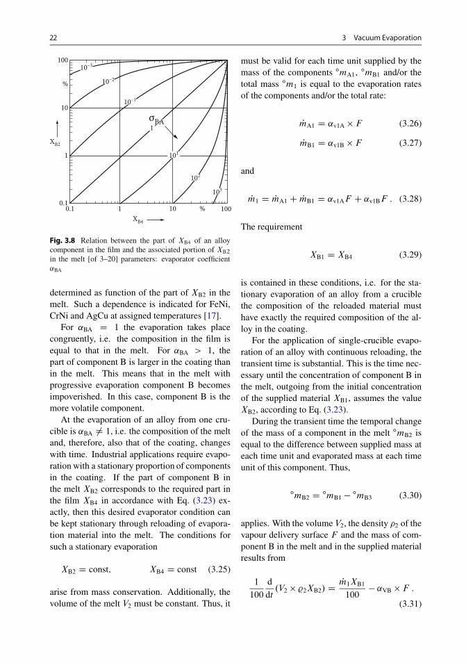
Fig. 3.8 Relation between the part of XB4 of an alloycomponent in the film and the associated portion of XB2
in the melt [of 3–20] parameters: evaporator coefficient˛BA
determined as function of the part of XB2 in themelt. Such a dependence is indicated for FeNi,CrNi and AgCu at assigned temperatures [17].
For ˛BA D 1 the evaporation takes placecongruently, i.e. the composition in the film isequal to that in the melt. For ˛BA > 1, thepart of component B is larger in the coating thanin the melt. This means that in the melt withprogressive evaporation component B becomesimpoverished. In this case, component B is themore volatile component.
At the evaporation of an alloy from one cru-cible is ˛BA ¤ 1, i.e. the composition of the meltand, therefore, also that of the coating, changeswith time. Industrial applications require evapo-ration with a stationary proportion of componentsin the coating. If the part of component B inthe melt XB2 corresponds to the required part inthe film XB4 in accordance with Eq. (3.23) ex-actly, then this desired evaporator condition canbe kept stationary through reloading of evapora-tion material into the melt. The conditions forsuch a stationary evaporation
XB2 D const; XB4 D const (3.25)
arise from mass conservation. Additionally, thevolume of the melt V2 must be constant. Thus, it
must be valid for each time unit supplied by themass of the components ımA1, ımB1 and/or thetotal mass ım1 is equal to the evaporation ratesof the components and/or the total rate:
PmA1 D ˛v1A � F (3.26)
PmB1 D ˛v1B � F (3.27)
and
Pm1 D PmA1 C PmB1 D ˛v1AF C ˛v1BF : (3.28)
The requirement
XB1 D XB4 (3.29)
is contained in these conditions, i.e. for the sta-tionary evaporation of an alloy from a cruciblethe composition of the reloaded material musthave exactly the required composition of the al-loy in the coating.
For the application of single-crucible evapo-ration of an alloy with continuous reloading, thetransient time is substantial. This is the time nec-essary until the concentration of component B inthe melt, outgoing from the initial concentrationof the supplied material XB1, assumes the valueXB2, according to Eq. (3.23).
During the transient time the temporal changeof the mass of a component in the melt ımB2 isequal to the difference between supplied mass ateach time unit and evaporated mass at each timeunit of this component. Thus,
ımB2 D ımB1 � ımB3 (3.30)
applies. With the volume V2, the density �2 of thevapour delivery surface F and the mass of com-ponent B in the melt and in the supplied materialresults from
1
100
d
dt.V2 � %2XB2/ D Pm1XB1
100� ˛VB � F :
(3.31)

3.3 Evaporation of Different Materials 23
According to Eqs. (3.9), (3.15) and (3.20) ˛vB
amounts to
˛vB D 4:4 � 10�4 � �B � pSB ��MB
T
� 12
� XB2
MB
�100�XB2
MAC XB2
MB
��1:
(3.32)
The solution of the differential equation(Eq. (3.31)) for the simple case is difficult, sincethe coefficient of activity is a function of themass parts, and all parameters are functions oftime and additionally partly of temperature. Thebehaviour is particularly confusing in the heatingup phase. For some materials the transient timehas been calculated by numeric integration [18].
In closed form Eq. (3.31) was solved on thebasis of different simplifications [19]. Sucha simplifying assumption exists in the follow-ing. During the transient time no reloading takesplace, i.e. ım1 D 0 applies. The time up to theformation of the melt is negligible in relation tothe transient time, and during this time no sub-stantial change of the composition of the meltsump takes place. The change in density duringthe entire transient time is negligibly small.
With this assumption Eq. (3.31) is given by
dXB2
dtD �100˛vB � F
V2%2: (3.33)
Additionally, if MA � MB, then with Eq. (3.32)we obtain
dt D �V2%2
�MBMA
�
4:4 � 10�4�B pSB�MBT
� 12 � F
dXB2
XB2:
(3.34)
During integration of t D 0 to t D tt withXB2.t D 0/ D XB1 and XB2.t D t1/ D XB2
we obtain for the transient time with stationarycondition XB1 D Xb3
tt D �t lnXB3
XB2: (3.35)
1 2 2010864
1
2
3
2010
6
4
100806040
4
3
h
2
1
tt
XB2(t–0)/X
B2(t–t
t)
0
0.5
0.2
1.5 τt
τt
Fig. 3.9 Transient time tt in dependence on the relation-ship of the mass component B in the melt at time t D 0
and t D tt (parameters: time constant �t in h)
�t is the time constant of the transition:
�t D�MBMA
�V2%2
4:4 � 10�4 � �B � pSB ��MBT
� 12 � F
:
(3.36)
With consideration of the simplifications we ob-tain the transient time �t (average values of thequantities V2, �2, F , pSB and �B are used for theevaporation temperature T ).
Figure 3.9 shows the transient time tt in de-pendence on the relationship of the mass compo-nent B in the melt at the time t D 0 and t D tt.
For the determination of the transient time ttwith the required part of XB4 D XB3 in the coat-ing, the corresponding concentration in the meltXB2 D XB2 .t D tt/ is to be calculated accordingto Eq. (3.23).
Parameters of the evaporator are the melt vol-ume V2 and the vapour delivery surface F influ-encing the time constant �t and thus the transienttime.
For example, during the evaporation of thealloy NiCr, if a composition of 80=20 in thecoating is required and if the evaporation takesplace at 2000 K, then �t D 1 h. For Cr contentXB2 one obtains a value of 3 % from Eq. (3.23).

24 3 Vacuum Evaporation
Fig. 3.10 Measured andcalculated values of theAg part in the layer XB4
as a function of the time tat the evaporation of anAgCu alloy at differentevaporation temperaturesTv until the stationarycondition is reached [18]
Measured and calculated Tv/K1710174518401910
0 100 600500400300200 1100s1000800 900700
100
70
50
30
80
60
40
20
XB4
t
10
The crucible is characterized by the relationshipV2=F D 0:7 cm. With these values a transienttime of 48 min occurs, until the stationary condi-tion is reached [19].
The transient time is a non-productive sec-ondary time and must, therefore, be reduced. Oneobtains a short transition time at a high evap-oration temperature with high vapour pressurepCB. With evaporation from crucibles with alarge melt volume, i.e. large values of the re-lationship V2=F , the transient time is long. Inorder to obtain a short transient time despite alarge relationship V2=F , a so-called starting in-sert in the crucible is used. This is a quantitywith the volume of the melt sump; its alloy com-position corresponds to the melt in the stationarycondition. The alloy material composition forthe reloading is equal to that of the film to beevaporated; this differs from the composition ofthe starting insert. On the basis of Eqs. (3.35)and (3.36) also the ability of the so-called flashevaporation [21] for the evaporation of alloys canbe seen. By removing volume V2 of the meltthe transient time is reduced; in the limit valueV2 ! 0 the transient time tt goes to zero. Ifthe material is inserted in small parts in an over-heated body, no melt slough is formed. With flashevaporation the concentration of component B ofthe supplied material XB1 is equal to XB3 in thevapour, always both at each time, and the easilyvolatile and less volatile components evaporatecompletely.
By analysis of the transient time the influenceof impurities by evaporation can be estimated.
Less volatile impurities, i.e. with small vapourpressure, have a large transient time, which is inmost cases large compared to the coating time.During evaporation thereby the part of impuri-ties is smaller in the coating than in the materialused. A disadvantage is that the melt with the lessvolatile impurities is enriched. Thus the evapora-tion rate is reduced.
During the transient time the alloy compo-sition of the film changes. Figure 3.10 showscalculated and measured curves for the temporaldevelopment of the composition during evapo-ration of an AgCu alloy [15]. One recognizesthat the concentration of the more volatile com-ponent, silver, is very high (80 to 90 %) at thebeginning of the evaporation, decreases with pro-gressive coating time. At the end of the transienttime a value of approximately 16 % is reached.
Figure 3.11 shows the increase of the transienttime of a silver copper alloy with an increasein the part of XB1 of the more volatile compo-nent in the supplied material. Further, it followsfrom this figure that: at low evaporation temper-atures the transient time can achieve such largevalues that for short time intervals, evaporationwith practically constant composition of the coat-ing components is possible.
For the AgCu alloy with 29.8 % Ag Ag at anevaporator temperature of 1625 K, within 2 minchanges the composition of the film only aboutapproximately 1 %. Depending upon the selectedtime, interval coatings with a silver part from 85to 90 % can be evaporated. This behaviour ofa melt is used for the production of alloy films by

3.3 Evaporation of Different Materials 25
Fig. 3.11 Measured andcalculated values of the Agfraction in the layer XB4
as a function of the time twith the evaporation of anAgCu alloy at differentevaporation temperaturesTv until the stationarycondition composition ofthe supplied material of29.8 % Ag is reached [18]
Measured and calculated Tv/K162517551770
0 100 600500400300200 1100s1000800 900700
100%
70
50
30
80
60
40
20
XB4
t
10
0 100 500400 s300200
a v/av(t
–tt)
t tt
1.2
1.0
0.8
0.6
0.4
0.2
1,4
Fig. 3.12 Relative evaporation rate ˛v=˛v.t D t1/ of thealloy AgCu (solid line) and the components Ag (dashedline) and/or Cu (dotted line) as a function of the time ttafter [18], final temperature Tv D 1785K, transient timett � 500 s, alloy AgCu with 8.06 % Ag
partial evaporation from a large molten reservoirwithout reloading. Since the necessary composi-tion of the melt, however, can be maintained onlyin a limited time interval, with this method of al-loy evaporation only a small part of the insertedmaterial can be utilized.
The time before the stationary condition isreached shows the total evaporation rate and theevaporation rates of the components character-istic changes, Fig. 3.12 [18]. As shown at thebeginning in the curves, during heating of theevaporation material, the evaporation rates risesteeply. This time is neglected in the preced-ing explanations for the determination of thetransient time. At the beginning of the evapo-ration process, this very high rate of the easilyvolatile component in the example Ag, is ev-ident in the high total evaporation rate. Thetotal rate is at first larger than in the stationarycase. Up to the end of the transient time theevaporation rate decreases from Ag constantly;the evaporation rate from copper in contrastrises.
Frequently, NiCr is used for the production ofresistance coatings and for corrosion protectivefilms, which can be evaporated from a cruciblewith continuous reloading. The vapour pressuresof Ni and Cr differ at an evaporation temperatureat Tv � 2000K approximately by a factor of 102.
The composition of the film after the end ofthe transient time is shown in Fig. 3.13. Theevaporation occurs from a water-cooled ring cru-cible with reloading in the form of a rod. Withthis method of alloy evaporation, a constant com-position of the coating can be obtained over manyhours. The fluctuations of the composition are inthe range of the analysis accuracy. Similar resultscan be reached with other alloys, such as Fe20Cr,other stainless steels of different composition andwith Cu10Al [25].

26 3 Vacuum Evaporation
Table 3.1 Comparison of the chemical analysis of evaporation properties and the vapour-deposited layer Ti6Al4V(average values in percent by weight)
Element Al V Fe C N O H Otherelements
Ti
Evaporation material 6.10 4.0 0.30max
0.08max
0.05max
0.20max
0.015max
0.4 Residual
Deposition layer 5.93 3.97 0.144 0.021 0.007 0.12 0.0051 0.4 Residual
1 20 65 h43
XNi
t
100%8070
Fig. 3.13 Nickel portion in the layerXNi with evaporationof NiCr 80=20 from a crucible with continuous charging
Also, for evaporating ternary alloys a constantcoating composition can be obtained after thetransient time. Foils from Ti6Al4V have been,e.g. manufactured by crucible evaporation withreloading [26].
A certain refining process from impurities isconnected with the evaporation. Table 3.1 showsthe results of the chemical analysis of the rawmaterial and vapour-deposited films. Due to thehigher purity, the values for the tensile strengthand bending stress of the vapour-deposited foilsare even higher than those of rolled material ofthe same thickness.
Alloys with strongly differing vapour pres-sures of components and fluctuations of the com-position of the alloys in the melt slough limit theevaporation of alloys from a crucible with con-tinuous reloading. Strong differences in vapourpressures leads to transient times that are toolarge.
The cause of fluctuations in the compositionof the melt slough can be temporal changes byelectron beam power or fluctuations in the heatlosses in the crucible. Such instabilities lead tochanges in the melt slough volume, which canlead to a composition change of the coating. Forthe dependence of the relative change of the morevolatile part in the coating of the relative melt, theslough volume is valid under neglect of the tem-
perature changes, and we obtain approximately:
�XB4
XB4D �V2
V2� XB1
XB2; (3.37)
whereby XB2 � XA2 and XB2 � XB4 are as-sumed. The concentration change in the filmthus depends on the change of the volume of themelt slough and on the relationship of the con-centrations in the feeded material and in the meltslough. Temperature gradients over the evapora-tor surface EF have an additional influence on thecomposition of the film [27].
With a relationship of the concentrationsXB1=XB2 of 100 for example a change of theproportional part of the component B in the film�XB4=XB4 of 10 % results in volume variation ofonly already 10�3.
The consequence of this influence of the vol-ume variations is that the method of the genera-tion of alloy films has its limits with evaporationfrom a melt slough with reloading if the vapourpressure of the components differs by more thanthe factor 103.
In special applications, fluctuations in the filmcomposition, which arise in the process of thefilm deposits, can be balanced by a thermal treat-ment process [28]. Most compounds dissociateby thermal evaporation, partial or complete, sothat thin films with stoichiometric compositioncannot be generated by simple evaporation.
3.3.3 Compounds
Not only the thermal dissociation, but also reac-tions with the crucible material limit the evapo-ration of compounds. These limits can be partlycompensated by use of electron beam evapora-tion [29].

3.3 Evaporation of Different Materials 27
The use of electron beams can induce diffi-culties at the evaporation of compounds, for ex-ample intensified dissociation by increased sur-face temperature of the evaporation material andcollision dissociation with the evaporated mate-rial [30]. Independently, whether a compound isevaporated by a conventional method or by elec-tron beams, the compound AxBy of the films, thefollowing applies:
y �NA
x �NB! 1 ; (3.38)
where NA=NB is the relationship of the atomicconcentrations of the components A and B in thefilm [31].
An important method of electron beam evapo-ration is reactive evaporation, i.e. the generationof a chemical compound during the evaporationprocess with a solid component and a gaseouscomponent. Another possibility to generate com-pound films is the evaporation of two compo-nents, which react by condensation on the sub-strate. In this way, a compound film Nb3Sn canbe generated by separate electron beam evapora-tion of niobium and tin. The rate of the condens-ing molecules ˛KAB for this type of generationof compounds by evaporation is proportional tothe product of the condensation rates of the com-ponents ˛KA and ˛BK and an average diffusioncoefficientD:
˛KAB D K � ˛KA � ˛KB �D : (3.39)
The condensation rates ˛Kt are proportional tothe vapour pressures pei of the components .i DA;B/ at the substrate and to the adhesion coeffi-cient or sticking coefficient ˇ:
˛Ki � ˇ.TS/ � pei : (3.40)
From these conditions it can be derived thatthere is a range for the vapour pressures pei atcertain substrate temperature TS, the so-calledstoichiometric interval in which only the com-pound AxBy condenses.
A variant of this procedure consists of evap-orating the components in the necessary rela-tionship, and generating the chemical compound
by means of a following temperature treatment.TiC coatings have been generated this way [32].By reaction of the condensing material with thesubstrate material or with adsorption films, thincoatings of a certain chemical composition canalso be generated. This type of generation of in-terface coatings plays an important role [33] inthe production of adhesive films or adhesive in-termediate films.
For reactive evaporation the pressure or partialpressure of the gaseous component necessary forthe reaction is fed in the recipient with pressuresof 10�4 to 10�3 mbar.
If the pressure of the reaction gas is chosento be too high, gas incorporation and losses ofenergy of the evaporated component cause toofrequent collisions of the vapour with the gas,which can have a negative influenced on the filmproperties. For the generation of oxide and/ornitride films as reaction gas, oxygen and/or ni-trogen is usually used. In special cases, theoxidation takes place also with the help of wa-ter vapour. For reactive evaporation of carbides,we use easily separable carbon compounds, likeC2H2 or C2H4. The generation of TiC, for exam-ple, takes place via the reaction
2Ti .vapour/C C2H2 .gas/
! 2TiC .film/C H2 .gas/ : (3.41)
In order to discuss influencing parameters duringreactive evaporation, it is assumed that an ad-sorption of the gaseous component precedes thereaction.
For the relationship of the components in thecoating after reaction with an adsorbed atomic re-action gas A is obtained:
NA
NB� vA
vB.1 ��/2 � Z
.Z ��/ � ˇA � e� ERTS :
(3.42)HerevA=vB is the collision number relationship of the
components on the substrate, the degree of coverage,Z the number of neighbour adsorption
places,E the activation energy of chemisorption,

28 3 Vacuum Evaporation
ˇA the condensation coefficient,R the gas constant, andTS the substrate temperature.The result of the reaction depends on the ther-modynamic conditions, in particular on the acti-vation energy, the temperature and the condensa-tion coefficient, which decide on the relationshipnumber of collided particles between the reactiongas and the number of condensing vapour parti-cles.
The collision number relationship vA=vB is:
vG
vD� 55:5MD pG
% ˛K;
wherevG in cm�2 s�1 is the surface-related impinge-
ment rate, i.e. the coefficient of restitution ofthe gas particles, which meet for each timeunit the unit area;
vD in cm�2 s�1 the surface-related impingementrate, i.e. the coefficient of restitution of thevapour particles, which meet for each timeunit the unit area;
MD the mass value of the vapour particles (thenumerical value corresponds to that of theatomic and/or molecular mass);
� in g cm�3 the density of the evaporation sub-stance;
pG in Pa (10�2 mbar) the gas pressure in the re-cipient;
˛A in nm s�1 the condensation rate; here thegrowth rate of the film.
In order to fulfil the condition of Eq. (3.38), i.e.to attain a stoichiometric composition of the filmthe relationship vA=vB must be much larger than1, because in Eq. (3.42) only part of the strikinggas particles is adsorbed. For reactive evapo-ration of SiO2, for example, Eq. (3.38) is onlyapproximately fulfilled for
vA=vB � 102 :The determining influence on the collision fre-quency relationship of NA=NB and thus on thefilm properties at reactive evaporation of SiO2 isillustrates in Fig. 3.14.
For high rate reactive evaporation a high par-tial pressure of the reaction gas must be used. At
1 100.1 100
£
γO2/γSiO
9
8
7
6
5
4
3
2
3.3 × 10⁻³
6 × 10⁻³
1.1 × 10⁻²
2.7 × 10⁻²
O2 partial pressure
pa
Fig. 3.14 Reactive evaporation of SiOx ; dependence ofthe dielectric constant " on the impact number relationshipO2
=SiO
a pressure of the reaction gas of 10�2 mbar themean free path of a vapour particle amounts toonly about 5mm. The volume collisions can nolonger be neglected against the surface collisions.
The limit for the increase of the reaction gaspressure depends on the scattering of vapour, andthe associated reduction of the evaporation rateand the utilization of material. In addition, lossesof energy of the vapour particles arise by scatter-ing.
The method of activated reactive evaporationis the probability of reaction with a certain col-lision frequency relationship increase, withoutincrease of the reaction gas pressure. The reac-tion gas, the vapour or both components mustbe activated. This can be done by ionizationmethods, for example, by microwaves, by meansof an electron beam or by an electrical dis-charge [31, 34]. An electrical discharge cangenerated between the evaporation materials andsubstrate with an electrode with a positive ornegative potential applied opposite the evapora-tion materials [32]. Depending on the polarity,negative or positive charge carriers strike the sub-strate. In the case of negative polarity on thesubstrate, the arrangements for activated reactiveevaporation are called ion plating.
For example, by activated reactive evaporationof titanium in reaction gas C2H2 with a high con-densation rate of 0.2 µm=s a common condensa-tion of Ti and C in the stoichiometric relationship
3.4 Vapour Distribution 29
was reached [31, 32]. At substrate temperaturesof around 1000 ıC a reaction of the componentswas obtained.
3.4 Vapour Distribution
3.4.1 Small Surface Evaporators
The outgoing vapour stream from an evaporatoris characterized by the vapour stream density dis-tribution .˛/. With this function (also calledevaporator characteristic) the film thickness dis-tribution on the substrates can be calculated ata given arrangement of the substrates relative tothe evaporator. For electron beam evaporationthe simple case of a point source [35] with thevapour stream density distribution .˛/ D const.has more or less a practical importance. Onlythe special case of crucibleless evaporation froma molten mass can be characterized by this distri-bution function.
A better approximation for small surface evap-orators is the following approach: the vapourstream that escapes from a plane surface ele-ment dF is given by
.˛/ D 0 cos˛ : (3.43)
Here.˛/ is the vapour stream density in a direction
with an angle ˛ to the normal of the vapourdelivery surface, and
0 the vapour stream density for ˛ D 0.Small surface evaporators are defined by the factthat the dimensions of the vapour delivery surfaceare small in relation to the distance of the sub-strate. The vapour stream density distribution ofsuch a small surface evaporator can be describedby Eq. (3.43). For a larger evaporator surface orextended source distribution, the vapour streamdensity is determined by summation of the evap-orator characteristic of individual small surfaceevaporators or surface elements.
Electron beam evaporators with a diameterDV of the crucible and a distance hV to the
substrate are to be regarded as small surface evap-orators if DV � hV.
During evaporation with an electron beamevaporator, the conditions of a small surfaceevaporator apply; there are a series of influences,by which the vapour stream density distributionis changed. The description by simple cosine dis-tribution is not sufficient for practical application.Influences that cause deviations of the evapora-tor characteristic of the electron beam evaporatorfrom the simple cosine distribution are shown inFig. 3.15.
Instead of a plane vapour delivery surfacea convex surface can be formed, if the moltenevaporation material has a high surface tensionand the crucible is not wetted. The expected tran-sition of the evaporator characteristic from thecosine distribution to the isotropic distribution ofa point evaporator has not been observed, so itmust be assumed that other influences are moresubstantial.
By using an electron beam a very high vapourpressure over the melt can be developed so thatthe vapour delivery surface is deformed. A con-cave vapour delivery surface leads to a strongerdecrease of the vapour stream density with theangle ˛ (Eq. (3.43)). In the same way, vapoursinks in the environment have an effect on thevapour delivery surface. If the distribution of thevapour stream is constrained by cold parts of thecrucible wall, then the influence on the vapourstream density distribution is called a chimney ef-fect.
At high evaporation rates a vapour cloudforms over the vapour delivery surface. By colli-sions of the vapour particles between themselvesa part of the particles does not strike the substratesurface. If the range of high vapour pressureis limited on the vapour delivery surface, thenthe expansion of the vapour particles outside ofthe vapour cloud is linear, and it is calculatedwith a corrected evaporator characteristic. Atsmall expansion and density of the vapour cloud,(i.e. if it can be assumed that the largest part ofthe vapour stream without multiple collisions ofthe particles), the correction can take place viaa summand that considers the isotropic behaviourof the colliding particles [36].

30 3 Vacuum Evaporation
Formation of a convex vapour-delivering surface by the surfacestress of the evaporation material
Disability of the vapour propagationby the crucible wall during insufficientcrucible feeding
Formation of a concave vapour-delivering surface by local increaseof vapour pressure
Formation of a vapour cloud, which worksin place of the vapour-delivering surface assource of the vapour stream
Smother
Fig. 3.15 Influence of the vapour delivery surface of real small surface evaporators on the vapour stream densitydistribution
An approach for the description of vapourstream density distribution of real small surfaceevaporators is a higher-order cosine function inthe form
.˛/ D 0 cosn ˛ ; (3.44)
with n > 1. A sufficiently exact description ofthe vapour stream density distribution of elec-tron beam evaporators by Eq. (3.44) in the anglerange up to 30ı with a not too high evaporationrate s is possible. Figure 3.16 shows the vapourstream density distribution of a 5 kW electronbeam evaporator. Eq. (3.44) with n � 2:5 is validup to an angle ˛ D 30ı for the vapour streamdensity.
With an increasing evaporation rate, whichmeans an increasing deformation of the meltingbath surface, a stronger directionality depen-dency is to be expected, i.e. the exponent n inEq. (3.44) depends on the evaporation rate
n D f .˛V/ ; (3.45)
whereby n increases with increasing evaporation.For a 12 kW transverse evaporator the correlationn D K˛
1=4v was found [33]. For condensation
rates in the range around 5 nm s�1 for the expo-nent n between 2 and 3, n can take values up to
30°
20° α = 0°10° 10° 20°
40°
50°
60°
70°
80°
90°
30°
40°
50°
60°
70°
80°
90°
Φ(α)
0
0.8
0.7
0.6
0.5
0.4
0.10.1
0.20.2
0.30.30.3
0.9
1Φ0
0.1
0.2
Fig. 3.16 Vapour pressure density distribution of a smallarea evaporator. 5-kW-electron beam evaporator:evaporation from a water-cooled crucible, evapora-tion rate 0:4 g=min. Curve 1 measured characteristic,Curve 2 cos ˛-distribution, Curve 3 cos2 ˛-distribution,Curve 4 cos3 ˛-distribution, 0 vapour stream density for˛ D 0, .˛/ vapour stream density with the angle ˛
6 [37] with rates within the range of 100 nm s�1.For the values mentioned, the distance betweenthe evaporator and substrate is 200–250mm.

3.4 Vapour Distribution 31
Fig. 3.17 The Determina-tion of the film thicknessdS on a flat substrate fromthe vapour stream densitydistribution. dFv vapourdelivery plane element,dFK.hv/ plane element onthe ball around the evap-orator with the radius hV,dFK.hS/ plane element onthe ball with the radius hS
dFS plane element in thesubstrate level
Substrate
Geometrical relations
For the vapour flow densitythe distance relation is valid
cos∝ = hv
hs
cos∝ = dFk(hs)
dFs
Φk(hs)Φk(hv)
hv2
hs2= = cos2∝
dFs
dFv
dFk(hs)
dFk(hv)
hs
∝
∝
For evaporation characteristics according toa cosine function of higher order, the influenceof a vapour cloud can be better described by thefollowing approximation [36]:
˚.˛/ D ˚0�1 � ˚is
˚0
�cosn ˛ C ˚is : (3.46)
is is the isotropic part of the vapour stream.At a low evaporation rate it depends on is andachieves a constant value with a rising rate. Forexample, at a 12 kW evaporator, is D 0:14 0constitutes this limit value, and a condensationrate of 5 nm=s, measured at a distance of 250mm,is reached. With Eq. (3.46) and the indicatedvalue for the isotropic part the experimentally de-termined vapour stream density distribution up to˛ D 50ı with an accuracy of 1 % can be de-scribed [36].
The calculation of the film thickness distri-bution on arbitrary substrate arrangements fromthe evaporator characteristic is demonstrated byan example. The film thickness distributionis searched for a planar substrate or a planarsubstrate arrangement parallel to the surface ofa small plane evaporator. At a small plane evap-orator vapour extinguished on a spherical dishsurface is condensed. Then we have
d.˛/ � .˛/ : (3.47)
For the film thickness on the planar substratedS.˛/ arises under use of the relations in
Fig. 3.17,
dS.˛/ � cos2 ˛.˛/ : (3.48)
If for the vapour stream density .˛/ a simplecosine distribution is used, then with Eq. (3.43)for the film thickness on a planar substrates
dS.˛/ � d0 cos4 ˛ (3.49)
is valid.In the case of the validity of Eq. (3.44), we
obtain
dS.˛/ D d0 cosnC3 ˛ ; (3.50)
where d0 is the film thickness for ˛ D 0.With tan ˛ D rS=hV and Eq. (3.50), we obtain
dS
d0D 1�1C
�rShV
�2nC3
2
; (3.51)
wherehV is the distance of the substrate level from the
evaporator, andrS the distance between the evaporator-normal
and the substrate.In Fig. 3.18 the relative film thickness distribu-tion of dS=d0 is illustrated as a function of rS=hV
for different vapour stream thickness distribution(n D 1–5). The film thickness distribution ofdS=d0 for n D 0 corresponds with point sourceevaporation [.˛/ D const].

32 3 Vacuum Evaporation
1.0
0.8
0.6
0.4
0.2
2.00.5
n
0 1 2 3 4 5
1.0 1.5rs/hV
d s/d0
dsrsd0
dF
hV α
Fig. 3.18 Course of the relative layer thickness dS=d0
on an flat substrate parallel to the vapour delivery planeelement dF as a function of relationship rS=hV for differ-ent vapour stream density distributions .˛/ D 0 cosn ˛
[.˛/ D 0 means D const: (point source)]
Instead of the calculation of the film thicknessdistribution from the vapour stream density dis-tribution after Eq. (3.44) with an exponent n > 1it is also possible to use a simple cosine distri-bution, i.e. n D 1, if a virtual source of vapouris introduced [37]. The virtual vapour source foran evaporator lies with strong directive efficiencyaround the value�h over the real vapour deliverysurface.
The distance between the virtual vapoursource and the substrate surface is h0
V, wherebyh0
V D hV � �h. An approximation of a cosn ˛distribution by a virtual cos˛ distribution is ap-plicable only for small values of the relationshiprS=hV. The distance of the virtual source h0
Vmust correspond to the relationship
"
1C�rS
h0V
�2#2D"
1C�rS
hV
�2#nC3
2
:
(3.52)The mathematical description by a virtual vapoursource simplifies the calculation of the film thick-ness on any substrate arrangements. The de-scription permits transferring the film thicknessdistributions calculated for a cos˛ characteristicby the Eq. 3.52 to those of the cosn ˛ character-istic of real evaporators. With the example of theevaporation of a plane substrate by a small sur-face evaporator with a cosn ˛ characteristic of thevapour stream density, it must calculate exactly
on the relative change of film thickness �dS=dS
on the substrate and on the utilization rate �m
of the evaporated material. On a plane substratethe relative change of film thickness according toEq. (3.50) is
�ds
dsD .nC 3/ � tan ˛ ��˛ : (3.53)
For substrates that are arranged in the range ofsmall angles .˛ � ˛�/, we obtain
�ds
ds� .nC 3/ � ˛2 : (3.54)
The relative change of film thickness is thuslarger when the exponent n is larger. Sinceby electron beam evaporators the exponent nincreases with rising evaporation rate, the unifor-mity of the film thickness degrades the presentsubstrate arrangement with increasing rate.
The relationship of the mass of the substrateto the total evaporated mass is called the utiliza-tion factor �m of the evaporated material. If thesubstrate is arranged within the angle ˛ to thenormal, then the utilization factor is also equal torelationship of the vapour stream .˛/ in a rightcircular cone with a half-cone angle ˛ to the totalvapour stream 0, which is assumed from a smallplane evaporator.
With Eq. (3.44), the calculation of the vapourstream density will be
�m D ˚.˛/
˚0D
R
0
˚.˛/ d˛
�=2R
0
˚.˛/ d˛
D
R
0
cosn ˛ sin ˛ d˛
�=2R
0
cosn ˛ sin ˛ d˛
: (3.55)
As a result of integration of Eq. (3.55), we obtain
�m D 1 � cosnC1 ˛ (3.56)
and for small angles ˛ approximately
�m � nC 12
˛2 : (3.57)

3.4 Vapour Distribution 33
One demands a value for evaporation of a planesubstrate configuration with a small surface evap-orator for a relative change of film thickness�dS=dS, for example, 5 � 10�2; thus a permis-sible angle ˛ results in � 1:1 � 10�1 � 6:5ı forn D 1 from Eq. (3.54). Even for n D 1 afterEq. (3.57) the utilization factor �m is only about1:3 � 10�2; less than 2 % of the vapour particlesarrive at the substrate.
In this evaporation configuration we do notreceive a sufficiently extended film thickness onlarge substrate surfaces. The utilization factor �m
is low. The most important principles to reacha homogeneous film are:� Distribution of the source strength on an ex-
panded vapour-delivery surface� Arrangement at the substrates on planes of the
same vapour stream density� Adjustment of the retention time of the sub-
strates in the vapour stream and the vapourstream
� Density distribution through relative motion� Correction of the film thickness distribution
by scattering with the use of increased gaspressure
� Correction of the vapour stream density distri-bution by means of shutters.
In numerous different substrate arrangementsthese principles or a combination of several ofthem are used, see, for example [37, 38].
3.4.2 Evaporation Arrangementswith Expanded SourceDistribution
A method for realization of an expanded sourcedistribution is to use a number of small surfaceevaporators. By optimization of the number, oneanother position and the evaporation rates the re-quired vapour stream density distribution can beobtained with consideration of the characteristicsof the individual evaporators.
The resulting film thickness distribution canbe determined by accumulation and/or by inte-gration from the film thickness distribution of theindividual evaporators. Frequently an arrange-
ment of several small surface evaporators in a lineis used. If the substrates are moved perpen-dicularly to this line, then a high uniformity offilm thickness can be achieved (Fig. 3.19). Thisevaporation principle will be used for tapes andsubstrates, which on plane carriers or on rotatingbaskets, are arranged.
Further, a required source distribution canbe obtained by using a large-scale crucible andelectron beam scanning over the surface of theevaporation material. With the constant powerof the electron beam the temperature distribu-tion and thus the site specific evaporation rateare functions of the retention time of the electronbeam on each point of the surface.
In the case of sinusoidal deflection of theelectron beam in the x-direction of a crucible,different retention times result along the deflec-tion path. At the points of reversal of the electronbeam path on the evaporation material the reten-tion time tw has a maximum. Figure 3.20 showshow the power density distribution of e.x/ canbe changed along the deflection path by varia-tion of the electron beam diameter dF and thedeflection amplitude. With the limited expansionof the vapour delivery surface to generate a con-stant film thickness on the complete substrate, thesource density within the range of substrate edgemust be increased. The power density within therange of the reversal points is increased by si-nusoidal deflection of the electron beam. Thus,a correction possibility for the film thickness dis-tribution, which is sufficient for many tasks, isgiven. A strong rise of a crossfall of the vapourstream density at the crucible edges leads to highfilm thickness uniformity on the substrate and re-duces the utilization factor �m of the evaporationmaterial.
For this reason it may be necessary for indi-vidual applications to select a deflection programwith more than two maxima of the power den-sity and herewith also the source density overthe deflection path leads (Fig. 3.21). In thisarrangement the programmed guidance of theelectron beam is generated by a combination ofa dynamic deflection field and a static reversalfield.

34 3 Vacuum Evaporation
1
0.8
0.6
0.4
0.2
0–300 3000 mm mm
mm
δ = 0.75
–300 3000 mm
δ = 0.07
–300 3000–150 150
δ = 0.11
–300 3000–100 100
–100 100
δ = 0.22
c
ba
d
Fig. 3.19 Improvement of the film thickness distributionof dS=d0 on vapourization of a plane substrate with thearrangement of several small surface evaporators in a line(calculated). a small surface evaporator, b four smallsurface evaporators, same distance between evaporators,same evaporation rate, c four small surface evaporators,
different distance between evaporators, same evaporationrate, d four small surface evaporators, same distance be-tween evaporators, different evaporation rate. Evaporatorsubstrate distance hv D 300mm, opening angle of thevapour stream 2˛ D 180ı , vapour stream density distri-bution .˛/ D 0 cos ˛ ı D .dSmax � dSmin/=d0
1/20x
e (x)
dF= 116
dF= 14
dF= 12
Fig. 3.20 Power density distribution of e.x/ on the evap-oration material along a deflection course of the length l ;sinusoidal deflection of the electron beam, parameter elec-tron beam diameter dF
3.4.3 Vapour Propagationwith Small Free Path Length
In the past considerations of the generation andpropagation of a vapour stream, it was consid-ered that essentially a straight line propagation ofthe vapour particles takes place. For explanationof deviations from vapour stream cosine densitydistribution, collisions of the vapour particles hadto be considered among themselves within therange of the vapour delivery surface.
With increasing vapour pressure or at high gaspressure interaction effects in the entire range be-tween evaporators and substrate take place. Inthese cases vapour no longer expands in a straightline, and the relations indicated in Sect. 3.4.1 and3.4.2 lose their relevance.

3.4 Vapour Distribution 35
Substrate (band)
Dynamicdeflectionfield
B = B0sinωt
Direction of motionof the substrate
Temporally constantdeflection
Large-scale crucible
Path of the electron beam and locationof the ranges of high source density
– I2
– I6
I6
I2
x
I
Evaporation characteristicΦ = Φ0cos3αBand width ICrucible width 4/3 IDistance of ranges of high source density 1/3 IDistance of ranges of high source density 2/5 Itw Retention time of the electron beamds/d0 Relative film thickness distribution on the band toward xdF Diameter of the electron beam on the evaporation material
tw
x
ds/d0
dF
Fig. 3.21 Realization of an expanded source distribution by programmed deflection of an electron beam toward x ofa large-plane crucible (schematized)
The propagation of vapour within the rangeof strong interaction effects of the vapour parti-cles among themselves and the vapour with thegas is characterized by the fact that the meanfree path of the vapour particles is small by colli-sions among themselves lD, the vapour particlesat collisions with gas particles lDG and/or thegas particles with collisions among themselves lGagainst the distance hV between evaporators andsubstrate.
It thus applies that
lDI lDGI lG � hV : (3.58)
These conditions for the expansion of vapourare obtained at a gas pressure of 10�2 mbar andwith a coating with an extremely high evapora-tion rate. Since under these circumstances eachvapour particle is scattered several times on the
way to the substrate surface, the initial orien-tation and initial energy of the particles are nolonger important when the particle strikes the sur-face. In place of a directed vapour stream areabetween evaporators and substrate a vapour cloudis formed, which can also surround the substrate.
Figure 3.22 describes the direction modifica-tion of the vapour particles by scattering in thevapour cloud. Whereas in the directed vapourstream the vapour particles that strike the sub-strate only have small direction differences de-pending on the diameter of the vapour deliverysurface and the distance between evaporatorsand substrate, each emission point P consideredwithin the vapour cloud can be a source of vapourparticles, which spread out in all directions.
In extreme cases, frequent interactions of thevapour distribution can be characterized by thepressure of vapour pD. Under these conditions

36 3 Vacuum Evaporation
dFv
p'
p'p'
p'
dFv
Substrate
Emissionpoint p
with intense scatteringwithout scattering
Fig. 3.22 Influence of the scattering on the direction ofan up point P in the proximity of the substrate of theoutgoing vapour particles. dFV is a vapour delivery two-dimensional element, P 0 are scattering centres
TaNi
FeCu
Al
1 2 5 10 20 50 100μm min–1
0.2
0.5
1
2
5
10Pa
2
10–3
10–2
10–1
5
2
5Torr
pe pe
aK
Fig. 3.23 Connection between the vapour pressure pE
within the range of the substrate and the condensation rate˛K (calculated under the assumption of Maxwell distribu-tion of the velocity of the particles in the vapour cloud andthe trap coefficient ˇ D 1)
and on the assumption that the condensation sur-face does not disturb the pressure ratio in thevapour cloud between the condensation rate ˛K
and the pressure of the evaporating material pD
in the environment of the substrate pE we obtain:
˛K D K.M;T /ˇpD ; (3.59)
with the correlation pD � pE.Figure 3.23 illustrates the vapour pressure pD
in the vapour cloud, which are necessary in orderto achieve a certain condensation rate under theconditions of large scattering processes.
If vapour particles are scattered at gas parti-cles, then pD in Eq. (3.59) is only the vapour
Substrate
100 mm
po in pa
300 10030 105 31 0.6
Fig. 3.24 Vapour pressure pD in the vapour cloud at elec-tron beam aluminium evaporation at a power of P0 D250 kW; power density is within the range of the focalspot, for instance, 2 � 107 W=m2
partial pressure. The energy of the condensingvapour particles is reduced by repeated colli-sions with gas particles in relation to their initialvalue. In the vapour cloud a mean free pathcan be indicated lD. For example, at condensa-tion of aluminium with a condensation rate of5000 nm=s in the environment of the substrate themean free path adds up to some millimetres. Fig-ure 3.24 illustrates the pressures pD in the cloudwith the evaporated aluminium with a power of250 kW.
The vapour pressures pD in certain distancesfrom the evaporator were calculated from thecondensation rate in accordance with Eq. (3.59).The values obtained in the environment of thevapour delivery surface were determined by ex-trapolation.
To which extent the scattering of the vapourparticles between themselves changes the filmthickness distribution is shown Fig. 3.25. A steelband was led across an evaporator crucible of500mm. The electron beam was once on a linein direction of motion of the steel band and an-other time on a line perpendicular to the steelband. Despite the very different distribution ofthe vapour source, there were only small differ-ences in the film thickness distributions on thesteel band.
At evaporations with small gas pressure andvery high vapour pressure no complete isotropy

3.5 Equipment Technology 37
4.0
3.0
2.0
1.0
0
μm
–200 0 mm 200
Film
thic
knes
s d
Band width b
Fig. 3.25 Influence of scattering of vapour particles withhigh vapour density on the film thickness distribution.Electron beam power 250 kW, programmed deflection ofthe electron beam in a direction: ı transverse to the steelstrap movement, � lengthwise to the steel strap move-ment. Crucible 500 � 500mm, distance of the strap fromthe evaporator surface � 200mm
within the range of the substrate prevails, i.e.the condensation is partly intended to occur bya vapour cloud, partly by a directed vapourstream.
With pressure plating [39], reactive vapouriza-tion and partially ion plating interaction of thevapour particles with gas particles is the causeof strong scattering of vapour. The transport ofthe evaporated material through the surroundinggas, takes place via diffusion, if the condition ofcomplete scattering is reached.
Within the range of the vapour deliverysurface the interaction with the gas leads tobackscattering of vapour. The decrease ofthe evaporation rate can be described, as inSect. 3.3.1, by the transmission coefficient � .
Advantages of scattering in the residual gasare the reduced shadow influence and half-shadow influence at unevenness and edges onthe substrate surface. Therefore, with scatteringcoating the degree of coverage in particular atrough surfaces is improved.
For the expansion of vapour under conditionsof extreme high vapour pressure and high gaspressure, a direct influence of the vapour streamwith increasing pressure has been observed [39].
Figure 3.26 shows the thickness distributionof films from stainless steel on a plane substratewith an evaporation rate of 32 g=min with differ-ent gas pressures.
–120–100 –80 –60 –40 –20 20 40 60 80 mm 1200
x
0
1
2
3
mm
ds
6.7 x 10⁻¹ Pa
13 x 10–3 Pa
1.3 Pa
2.7 Pa
3.3 Pa
4.0 Pa
9.3 Pa
Fig. 3.26 Film thickness distributions on an flat sub-strate at vapourization with an extremely high evaporationrate for different gas pressures [39]; transverse evapora-tor, evaporation rate ˛v D 32 g=min remains constantduring pressure increase, compensation of the changedtransmission through an increase of the output of 60 kW(p < 10�4 mbar) up to 102 kW (p D 10�2 mbar); work-ing gas argon, distance evaporator substrate 324mm
3.5 Equipment Technology
3.5.1 Prefaces
When designing evaporation equipment the de-mands in each case, which can be very different,are considered, for example,� Purity of the film� Film thickness� Film thickness tolerances� Film morphology� Single film or film system� Coating process, for example, reactive coating� Additional ionization, sources of plasma� Substrate material (glass, plastic, paper, metal,
chemical compounds)� Substrate form (bulk material, shaped parts,
foils)

38 3 Vacuum Evaporation
� Substrate size� Degree of automation.
3.5.2 Auxiliary Equipmentfor Evaporation Plants
3.5.2.1 Evaporation Sources3.5.2.1.1 GeneralDuring coating, the substrates move overa vapour source. The substrates rotate simplyor doubly in order to achieve as good film ho-mogeneity as possible. The material therebygenerally evaporates from bottom to top. Withthe appropriate construction of the evaporationsources, however not with all materials, evapo-ration is also possible in the reverse direction orsidewise.
Some decisive factors for the choice of the sortof evaporator sources are:� Film purity� Condensation rate and film thickness� Temperature of the substrates during the coat-
ing� Type of coating material.Only a small part of the energy supplied tothe evaporator is needed for the actual evapora-tion process, for transformation of a solid intoa vapour.
The largest part of the energy is lost throughthermal conduction over the energy supply cableand/or over the more or less well-cooled wall, forheating the coating material in the crucible andthrough thermal radiation. Circa half of the sup-plied energy is exhausted for water cooling. Theenergy lost through radiation is not considerableand is calculated after Stefan Boltzmann’s law:
ES D At"T 4 : (3.60)
HereES is energy in Ws,A the surface of the radiation source in cm2,T the temperature of the radiation source in K, the radiation constant of a black body (5:67�
10�2 W cm�2 Grad�4/," the correction factor, andt the duration of the test in seconds.
3.5.2.1.2 Resistance-Heated EvaporationSources
Because of the simple handling and thesmall complexity resistance-heated evaporationsources are nowadays still frequently used. Nu-merous sizes and forms (e.g. spirals, cavities,boxes without covers or with perforated covers)are commercially available. They are usuallymanufactured from materials with high melt-ing points, such as tungsten, molybdenum ortantalum. For coating materials with low evapo-ration temperatures (for example, tellurium, sele-nium) stainless steels are also used as evaporationsource materials. Figures 3.27 to 3.39 showthe most commonly used forms of evaporationsource.
Tungsten spirals are used for highly reflec-tive evaporating aluminium mirrors. Aluminiumwires are put, for example, in hairpins form intoa spiral coil [40]. Trough-shaped evaporation
Fig. 3.27 Hairpin-shaped evaporator with twisted tung-sten wire
Fig. 3.28 Spiral evaporator from twisted tungsten wire
Fig. 3.29 Basket-shaped evaporator
Fig. 3.30 Trough-shaped evaporator

3.5 Equipment Technology 39
Fig. 3.31 Box-shaped evaporator
Fig. 3.32 Source of evaporation with ceramic crucible
Fig. 3.33 Evaporator with vapour jet turn with roundsheets
Fig. 3.34 Trough-shaped evaporator with ceramic coat-ing
a a
Fig. 3.35 Evaporator with vapour jet turn with roundsheets for evaporation from bottom to top, refilling open-ing
a a
Fig. 3.36 Evaporator with steam jet with round sheets forevaporation from top to bottom refilling opening
a
b
c
d
Fig. 3.37 Sublimation of chrome. a chrome holder, b tan-talum heater, c radiation protection, d tungsten carrier
sources can be regarded in good approximationas point-shaped evaporation sources; they pro-duce a rotationally symmetric vapour lobe.
Box-shaped evaporation sources are used iflarger material quantities are to be evaporated.With a perforated cover plate larger losses areavoidable. The cover plate temperature shouldin no case be lower than the evaporation temper-ature, since otherwise the danger of condensationexists and thus the openings in the perforated

40 3 Vacuum Evaporation
b
a
Fig. 3.38 Evaporator using ceramic(s). a ceramic cru-cible, b tantalum heater
a
b
Fig. 3.39 Evaporator with inductive heating. a high-frequency coil, b ceramic insulators
cover plate can be closed. This can lead toa complete interruption of the coating process.Sublimating materials in pill form or granulates
such as silicon monoxides or zinc sulphides arealmost exclusively evaporated with covered evap-oration sources.
With evaporation from top to bottomresistance-heated evaporation sources receivea heated roof-shaped cover plate, which causesa deflection of the vapour stream. However, thetemperature of the deflection plate must be sohigh that no condensation takes place. Occasion-ally one provides trough boats with a ceramiccoat or with a ceramic cartridge for the extensionof the life cycle.
For evaporation of larger material quantitiesduring longer periods, for example, coating foilsin coil coating plants, cuboid-formed evapora-tion sources from semiconducting materials, forexample, boride or nitride, are used. They areheated by direct current and held by water-cooledclamping tools, which the thermally caused di-mension changes of the evaporation source bycounter bearings adjust. The usually wire-shapedcoating material is continuously supplied by un-spooling from a supply roll.
Typical wire diameters are 1–2 mm. Abovethe unwinding speed and temperature of the evap-oration source, the evaporation speed and inconnection with the speed of the foil the de-sired film thickness can be adjusted. From anevaporation source with an evaporating surfaceof about 1000mm2 about 4:5 g=min aluminiumcan be evaporated splash-free [41–44].
One method used with certain materials forevaporation is to sublimate wires or metalsheets [45]. A condition is a sufficiently highsublimation rate below the melting point of thecoating material. For example, with a coatingrate of 10�4 g cm�2 s�1, materials for sublima-tion are Ti, Zr, Fe and Zn.
3.5.2.2 Electron Beam Evaporators3.5.2.2.1 PrinciplesAn electron beam evaporator consists of an elec-tron beam gun and a crucible. In many casesthis configuration is supplemented by a charg-ing device for the evaporation material. Withmany evaporator constructions the mechanismsfor electron emitter generation and electron beam

3.5 Equipment Technology 41
a b
c
d
e
f
Cathode
Electrode atcathode potential
Electron current
Vapour flow
Evaporation material
Control electrodeAnode
Electron beam
Water-cooledcrucible
Magnetic lens
Magnetic transverse field
Ring electrode
Ring cathode
UB
UB
UB
UB
UB
UB
Fig. 3.40 Principles of electron beam evaporators.a Evaporator with electron collision heating, linear cath-ode and electrostatic focusing; b evaporator with electroncollision heating, ring cathode and electrostatic focusing;c evaporator with axial gun and electrostatic long distance
focusing; d evaporator with electron collision heating,ring cathode; electrostatic focusing and deflection; e evap-orator with axial gun, magnetic focusing and magnetic90ı deflection; f evaporator with transverse gun and mag-netic 180ı deflection
guidance, as well as the crucible in a unit arecombined.
Electron beam evaporators operate accord-ing to different principles, which are shown inFig. 3.40. In simple arrangements with electroncollision heating a cathode in the environmentof the evaporation material and/or the crucibleis used. The electrons flow with an acceleratingvoltage between cathode and crucible, directedtowards the evaporation material.
In order to focus the electron current at a cer-tain diameter on the evaporation material, a con-trol electrode at the cathode potential is used.If ring cathodes are used, then the control elec-trode also has the form of a ring concentricallysurrounding the crucible. Evaporators from thistype of ring source were developed in differentversions. Because the cathode is arranged in theenvironment of the evaporation material, a con-tamination of the evaporated film by evaporation

42 3 Vacuum Evaporation
of the cathode material can occur. A suitableform of the gate electrode avoids the evaporatingcathode material striking directly the substrate.
The arrangement of high voltage-guided partsin the direct environment of the vapour sourceleads to high voltage discharges and glow dis-charges between cathode and crucible. The dan-ger of such disturbances increases with increas-ing evaporation rate and accelerating voltage.The vapour pressure in the environment of evapo-ration material with ring sources may not exceedthe range from 10�3 to 10�4 mbar. The accelerat-ing voltage used is generally smaller than 10 kV,usually only 3–5 kV. Because of the limitation ofthese parameters the application of ring sourcesis reduced to a power range up to approximately3 kW. The maximum evaporation rate dependson the evaporation material, the power and thevapourization geometry. The condensation ratesattainable with such electron beam evaporatorsare within the range of 1–10 nm=s with a distancebetween evaporators and substrate of 250mm.
When an additional anode is arranged in therange between the cathode, the control elec-trode and the crucible, the electron beam can beformed. An advantage of this principle is that therange between beam generator and vapour sourceis field free; electron beam generation and evap-oration are separate.
Another way is the use of a magnetic lens tofocus the electron beam. The arrangement of agun over the crucible has the disadvantage thatthe gun is in the direct vapour stream. Thus,not only is the vapourization of the gun dis-turbed, but also the usable range, within whichthe substrates can be arranged is restricted be-cause of shadowing parts of the electron emitter.These disadvantages can be avoided, if the gunis arranged horizontally and the electron beam isdeflected electrostatically or magnetically beforestriking the evaporation material.
The separation of the electron beam genera-tion from the crucible, the magnetic deflectionof the electron beam before it strikes the surfaceof the evaporation material and the use of lin-ear cathodes is realized with transverse electronevaporators. The electron beam is usually de-flected at about an angle of 180ı or 270ı.
AS
K
RK
ϑ
RA
Fig. 3.41 Emergence of a beam producer after Piercefrom a ball diode. A anode, K cathode, S edge of beam,RA anode radius, RK cathode radius, @ half opening an-gles
High power axial guns, such as those used forelectron beam evaporators, are often character-ized by means of a space charge magnitude, theperveance. The perveance is indicated in units of10�6 A=V3=2 D µP.
Electron beam characterization with highcurrent densities goes back to the theory ofJ.R. Pierce. The theory is valid up to perveancesof approximately 1 µP. Concentrated space conescut the cathode out of the outside ball and the an-ode out of the inside ball (see, Fig. 3.41).
With negative space charge, without the fo-cusing electrode the beam would expand itselfalready before the anode, which would lead toanode loss and/or reduced perveance values. Theform of this electrode cannot be calculated ana-lytically and is determined experimentally or bynumerical computer calculations.
The potential deformation by the anode open-ing can be considered by the fact that it isattributed the characteristic of a dispersing lenswith the focal length f D � � 4V=V 0 (V Danode potential, V 0 D gradient on the cathodeside). For perveance values larger than 1 µP thetheory is no longer valid, since the anode openingcomes into the order of magnitude of the distancebetween cathode and anode, so that the potentialdeformation becomes inadmissibly large by the

3.5 Equipment Technology 43
d fZmin
P = 0.12 × 10⁻⁶ A/V3/2
RA
RK
rArK
Ta
Ta
β
α
CCu
rmin
r
Zϑ
Fig. 3.42 Dimensioning of a Pierce beam generator of0.12 µP (10 kV, 0:1A). rK D 3mm, rA D 1:5mm,RK D 27:08mm, RA D 13:54mm, rmin D 0:87mm,
f D 33mm, d D 13:54mm, Zmin D 25:7mm, sin# D0:1108, # D 6ı 20ı , ˛ D 24ı , ˇ D 29ı
bc
a
d g if
e h jk
Fig. 3.43 Cut by 25KW ES evaporator with a Piercebeam generator and 90ı beam deflection. a electron beam,b copper one dish crucible, c deflection coil, d anode, e fo-
cusing coil, f focusing electrode, g high voltage insulator,h water cooling, i radiator box, j protection hood with fan,k separate evacuation
anode opening. Large anode current losses andstrong beam divergences result.
With special emitting surfaces like concentrictoroids, which generate hollow beams, perveancevalues to 60 µP can be reached. Figure 3.42shows the result of a calculation for a beam gen-eration system of 0:12 µP (10 kV, 0:1A) witha Ta cathode of 6mm in diameter. Industrialevaporators using Pierce beam generators havebeen used in many different applications.
Figure 3.43 shows the schema of a 90ı elec-tron beam evaporator, which is used in the powerrange of 10–30 kW. The electron beam passesthrough a crossed deflection field after the focus-
ing lens, which in addition to the 90ı deflectionpermits stirring the beam in the crucible.
3.5.2.2.2 Integrated GunsFor the installation into different vacuum recip-ients small and compact guns were developed.At both sides of the crucible magnetic transversefields are arranged, which operate as electrontraps (Fig. 3.44). The paths of the scattered elec-trons drift mirror symmetrically to the incidentbeam. In this way, the scattered electrons strikein the water-cooled plates in a defined way.
The plane beam of a transverse gun generatesan elongated focal spot in the crucible, whose

44 3 Vacuum Evaporation
Target platesfor backscatteredelectrons
Transverse evaporator
Magnetic transversefield
Paths of simple and doublebackscattered electrons
Primaryelectron-beam
Fig. 3.44 Effect of the magnetic transverse field ex-panded over the crucible as a trap for backscatteredelectrons
small axle measures 1–5mm. The length of thefocal spot depends very strongly on the powerand at 15 kW it is between 10 and 15mm. In or-der to disperse the electron beam power on theevaporation material, the electron beam predom-inantly wobbles in the direction toward the smallaxle of the focal spot. The wobbling usually oc-
Fig. 3.45 Intersection by6 kW an electron beamevaporator with 180ı jetdeflection. a beamgenerator, b x-deflectioncoil, c y-deflection coil,d water-cooled coppercrucibles, e electron beam
b
d
e
a
c
curs with deflection frequencies within the rangeof 50 cycles per second up to 400 cycles persecond. According to the different operating con-ditions, evaporators with transverse guns in thepower ranges up to 4 kW, 5–7 kW and 12–15 kWare manufactured as standard components. Withthe standard types, the maximum acceleratingvoltage has values within the range of 10–15 kV.In special cases also evaporators with outputs of20–10 kW are used. Much beam transverse evap-orator equipment is implemented for an output of200 kW.
Figure 3.45 shows the technical design ofa transverse evaporator.
3.5.3 Electron Emission
3.5.3.1 Generation of Free ElectronsFree electrons are obtained from solid, liquid andgaseous materials. The emission of electronsfrom liquid material does not play a role with

3.5 Equipment Technology 45
electron guns. For the generation of electronsfrom gas discharges with cold cathodes and mag-netically concentrated low pressure plasmas withlow discharge voltage are used [46].
Electron emission from solid materials hasgained technical importance. As emitters forelectron guns mainly glow cathodes are used.The emission current density is jeT and theRichardson–Dushman law describes the tem-perature determined saturation current densityachievable with these cathodes,
jeT D AT 2e�B=T : (3.61)
HereA is the Richardson constant,B the characteristic sizeB D eUA=k of the elec-
tron work function eUA, andT the absolute temperature.The quantities A and B are material-dependent;they are well-known as possible cathode materi-als.
Tungsten, tantalum and lanthan hexaboride.LaB6/ are the most common materials. Fig-ure 3.46 shows the dependence of the saturationcurrent density of these materials as a function ofthe cathode temperature. The upper limit for theusable emission current density depends on tem-perature stability and the material evaporationtaking place at high cathode temperature. Thecurrent emission density of tungsten occurs at 1–10A=cm2. In special cases with reduced lifetimea current density of 15–20A=cm2 is reached.
Other cathode materials, such as, for exam-ple, LaB6 or other activated cathodes used toobtain as low an emission temperature as possi-ble at high emission current density. Tungsten isthe most important cathode material for electronbeam guns. Further, tantalum, LaB6 and tung-sten with emission increasing alloy componentsare also used. At a given cathode temperature thesaturation current density can only be achievedaccording to Eq. (3.46) if the electrical field in-tensity before the emitting surface is high enoughto suck up all escaped electrons. If this conditionis not fulfilled, an electrode cloud is formed be-fore the cathode.
1500 1600 1700 1800 2000 30002500 K
1327 1527 1727 2227 2727 C°100
10
1
10–1
10–2
A cm–2
jeT
TK
Fig. 3.46 Saturation current density jeT for commoncathode materials as a function of the cathode temperatureTK, I LaB6 on carbonized tantalum, II tantalum, III tung-sten, work areas strengths drawn
The space charge of this electron cloudchanges the field gradient in such a manner thatfurther emission from the cathode surface is lim-ited. The space charge limited emission currentdensity jeQ arises on the basis of the Child Lang-muir law,
jeQ D 2:3 � 10�6K U 3=2B I (3.62)
wherejeQ in A=cm2 (Fig. 3.47),UB in V is the accelerating voltage,K in cm�2 a variable dependent on geometry,
which in the simplest case of flat parallelelectrodes amounts to K D 1=Z2
KA, andZZA means the distance between cathode and an-
ode.The space charge limited current density has beencalculated also for other electrode shapes. At agiven accelerating voltage and distance betweencathode and anode, the space charge limited cur-rent density can be changed through the geometryof the field-generated adjustment.
Through the curvature of the potential sur-faces the use of small-plane cathodes causes anincrease of the field strength at the cathode andthus an increased space charge limited currentdensity, which are described by K > 1=Z2
KAin Eq. (3.62). This effect is used with three-

46 3 Vacuum Evaporation
103
A cm–2
102
10–1
10–2
10
1jeQ
102 103 104 105 10610
UB
V
0.1
1
10
5020
Z KA =
100m
m
Fig. 3.47 Space charge limited emission current densityjeQ as a function of the accelerating voltage UB with ar-rangement of cathode and anode in parallel levels with thedistance ZKA
electrode beam generators in order to increase thespace charge limited emission stream adverse toa plane arrangement by a factor of 2 to 5.
By means of field emission the current densityjeE is described by the Fowler–Nordheim rela-tionship. On simplification the assumption of thiscurrent density in A=cm2 is
jeE D 1:54 � 10�6 E2
UA
� exp�6:83 � 107 U 3=2
A =E�; (3.63)
whereE is the field strength in V=cm, andeUA the electron work function in eV.In the case of an electron work function of 4:5 eV,a field emission current density in the case ofa field strength of 3�107V=cm of approximately102 A=cm is reached.
3.5.3.2 Calculation of BeamGeneratorsFor dimensioning of beam generators by meansof numerical calculations, the electron beam inthe beam generator is characterized by a numberof electron trajectories, which are extinguished
from the cathode. The envelope of these elec-tron trajectories describes the form of the electronbeam and thus the parameters in the smallestbeam diameter and/or focal spot.
The electron trajectories must thus be calcu-lated for an emitter configuration that can bedescribed in each case (Fig. 3.48).
The result of such a calculation is the potentialdistribution in the beam generator, the electronpaths and therewith the envelope and the spacecharge distribution. The current density distri-bution and/or power density distribution at thecathode and in given cross-sections of the beamgenerator are also calculated. Additionally, per-veance is usually also determined.
For the calculation the equations that describethe electron emission and the electron trajectoriesin the beam generator are to be used. If one limitsthe description to electrostatic systems, then thisentails the following physical relations:� The distribution of the electrical potential U
in the beam generator is determined by thePoisson differential equation. With the ge-ometrical arrangement of the electrodes andtheir potentials – the cathode potential UK, thecontrol electrode potential US and the anodepotential UA – the boundary values for thesolution of this equation are given.
� The force, which acts to an electron in theelectrical field, results in the electrons’ equa-tion of motion. The solution of the equationrequires the knowledge of the potential U andthe electrical field strength E, also the gradi-ents of the potential U in each point of thebeam generator.
� The space charge distribution of �, in the spe-cial case only those of the produced electronbeam, changes the potential distribution U
and is therefore because of the influence onU also to consider.
� The electron emission of the cathode resultsfrom one of the Eqs. (3.61) to (3.63). Is theemission space charge limited, then the elec-trons are sucked up from the space chargecloud in front of the cathode.According to Eq. (3.62) the emission currentdensity is a function of the electrical poten-tial U in front of the cathode surface. From

3.5 Equipment Technology 47
controlelectrodecontrolelectrode
MM–1MM–1
USUS
j+1jj–1
j+1jj–1
r
Δr Δz
y+1
y
i–1i–1 i+1i+1 N–1N–1dB/2dB/2 NNiiz
Grid
rjr i rj+1,r i+1
rj+1ri
Z=i
Q1
Z=i+1
Q2
Q4
Q3
Envelope of the electron trajectories
Bahn
Cath
ode,
UK
Grid point P(i,j)
Anode, UAAnode, UA
Fig. 3.48 Meridian intersection electrostatic beam gen-erator with orthogonal coordinate lattice of r; z. �r;�zlattice spacing, N � M number of grid points, electrontrajectories 1– C 1, elementary current tube betweenelectron trajectories and C 1 with the current I� in
a cathode zone, ri ordinate of the path for z D i , r 0
iD
dr=dz gradient of the path for z D i , Q1 . . . Q4 pointsof environment of the path section between z D i andz D i C 1, dB of smallest beam diameter
there the regulation of the emission currentdensity requires the knowledge of the poten-tial distribution U .
The solution of the potential equation withoutspace charge takes place by means of a grad-ual approximation, likewise the solution of thepath equation. Because of the influence of thespace charge distribution on the potential and therelationship of the potential with the emissioncurrent density and/or the electron trajectories,the functional dependence cannot be calculatedindependently with gradual approximation withthe space charge distribution. The solution ofthe total problem, therefore, requires an iterativeapproximation procedure. For the determinationof the potential distribution U Poisson’s equationmust solve
�U D � %"0; (3.64)
where� is the Laplace differential operator, and� the space charge distribution.For calculation of the initial potential distributionthe Laplace equation is used
�U D 0 ; (3.65)
with � D 0. The electrostatic field in an axialbeam is rotationally symmetric; thus,
U D U.r; z/ ; @U
@'D 0 : (3.66)
In this case, the problem reduces to a two-dimensional problem with the coordinate z, theaxle of the beam generator and r the distancefrom the axle. With these coordinates andEq. (3.64) the following form is obtained:
@2U
@r2C 1
r
@U
@rC @2U
@z2D � %
"0: (3.67)
Numerically this differential equation can besolved by replacing it with a system of differentequations.
The transition of the differential equationEq. (3.67) to a system of difference equationstakes place via development of the potential Uin the environment of each point P.i; j / intoa Taylor array after the lattice spacing �� and/or��. This way, the potential in a grid pointP.i; j / is represented by its four points of neigh-bour P.i � 1; j /, P.i C 1; j /, P.i; j � 1/ andP.i; j C1/. For the potential in the point P.i; j /

48 3 Vacuum Evaporation
the linear relationship generally results in
U.i; j / D C1 U.i � 1; j /C C2 U.i C 1; j /C C3 U.i; j � 1/C C4U.i; j C 1/C C5%.i; j / : (3.68)
The coefficients C1 . . . C5 are functions of thelattice spacing �r , �z and the coordinate r .Eq. (3.68) represents the system of the differenceequations; their number corresponds to the num-ber of the grid points N �M .
In the special case of a square lattice with�r D �z D h,
U.i; j / D 1
4ŒU.i � 1; j /C U.i C 1; j /
C U.i; j � 1/C U.i; j C 1/�C h
8 riŒU.i; j C 1/C U.i; j � 1/�
C h2
"0%.i; j / ; (3.69)
which is valid for r ¤ 0. It is to be consideredthat for points on the axle P.i; 0/, because of theelement with the factor 1=r in Eq. (3.67) and/or(3.69), the relationship for U.i; 0/ must be mod-ified. The solution of the difference equations isachieved via an interactive computing procedure,whereby first a potential distribution U0.i; j /
without space charge is determined, which theLaplace equation (Eq. (3.65)) fulfils. In the nextapproximation steps, in each case the separatelycalculated space charge distribution is consid-ered; this way improved potential values Un.i; j /arise. The calculation must be repeated until theapproximations Un�1 and Un apply:
jUn � Un�1j < " ; (3.70)
i.e., until for two following each other approxi-mations the difference of the potentials is in allgrid points as a given bound ".
The convergence of the calculation procedureis thereby protected and/or accelerated by a re-laxation technology [47]. This technology meansthat for the next approximation not the valuesUn.i; j / are used, calculated with the nth step,
but corrected values U �.i; j /, which result fromUn�1 and Un:
U �n D U �
n�1 C ˇ�Un � U �
n�1�: (3.71)
Here ˇ is the relaxation coefficient.The calculation of the potential takes place
with overcorrection, i.e. it applies for 1 < ˇ < 2.The electron trajectories are calculated by meansof the motion equation of the electrons. If anelectron with the velocity Ev in an electrical fieldof the field strength EE and in a magnetic fieldof the induction EB moves, then the Lorenz forceacting on the electron is:
EF D �e. EE C � � EB/ : (3.72)
Neglecting relativistic effects, thus v � c, weobtained for the motion equation
md�
dtD �e. EE C � � EB/ : (3.73)
By means of this equation the electron trajec-tories can be calculated not only in the beamgenerator, but also in the beam guiding system.B D 0 is limited on electrostatic axial beam gen-erators, and Eq. (3.73) is simplified to
md2r
dt2D �e Er D �e @U
@r
md2z
dt2D �"Ez D �e @U
@z; (3.74)
where Et and Ez are the values of the compo-nents of the electrical field strength. The time tcan be eliminate by means of the energy theorem
1
2m
"�dr
dt
�2C�
dz
dt
�2#
D �e U : (3.75)
We obtain the non-linear differential equation ofsecond order for the electron paths in level r; z,
d2r
dz2D 1
2U
"
1C�
dr
dz
�2#�@U
@r� dr
dz
@U
@z
�:
(3.76)The numerical calculation of the paths cantake place via procedures of rational extrapola-tion [47] or via the Runge–Kutta procedure. The

3.5 Equipment Technology 49
procedure supplies the ordinate r and the upwardgradient dr=dz of the electron trajectories for onepoint with the abscissa z D iC1 from the valuesr and dr=dz of the abscissa z D i .
In addition, riC1 and driC1=dz are determinedby the potential U in each case, and the compo-nents of the electrical field at four points Q.k; l/of the surroundings, which is between z D i andz D iC1 (see Fig. 3.50). In addition to the matrixwith the values U.i; j / for the grid points P , thevalues U.k; l/ are still necessary for the pointsQand the values of the derivatives of the potential@U=@r .k; l/ and @U=@z .k; l/ for the path calcu-lation. For the calculation of the linear equationsfor the path, we obtained the following form:
riC1 D ri C f"�U;@U
@r;@U
@z
�
Q1
I I�U;@U
@r;@U
@z
�
Q4
#
driC1dzD dri
dzC g
"�U;@U
@r;@U
@z
�
Q1
I I�U;@U
@r;@U
@z
�
Q4
#
:
(3.77)
The starting points of the paths .r0; z0/ arearranged at a small distance in front of the cath-ode; the initial directions lie perpendicularly tothe cathode surface. The number of paths thatcan be computed determines the number of ini-tial points. In addition, the cathode is dividedinto zones and a path is assigned to each zone.The values r are then gradually determined by thecalculation procedure and dr=dz determines thepaths toward the z-axis. To calculate the spacecharge distribution of � from the relationship, weuse
j D % � v : (3.78)
A way to numerically calculate the space chargedistribution is to determine the current density in-side elementary current tubes, which are formedin each case from the two neighbouring paths ac-cording to the selected zones of the cathode. Thecurrent in a current tube between two paths and
C1 of a cathode zone is the space charge limitedcurrent of this zone. In this procedure, the currentdensity j.z/ is reversely proportional to the dis-tance of the neighbouring paths and C 1.
The part of a current tube for the space chargein the grid point P.i; j / thus comes from thecurrent of the current tube, which calculates thevalues r and dr=dz, the paths r and r C 1 andthe values U.i; j /. The space charge �.i; j / thenresults from the sum of the mean space chargesof the current tubes, which decline into each gridpoint when assigned an influence zone.
For the calculation of the values �.i; j / a re-laxation procedure with a correction factor � isused
%n D %n�1 C � .%n � %n�1/ ; (3.79)
with 0 < � < 1.Another method for the determination of the
space charge distribution of each cathode zone isby the use of representative related paths, whichcome out from the centre of the cathode zone. Inthis case, the delay time of the electrons on eachpath in a lattice mesh and the reciprocal distanceto the grid point their space charge contributionfor this grid point are determined.
The current density at the initial points nearthe cathode surface jeQ; and thus the current of anelementary tube in and/or a representative path iscalculated with the help of the space charge law.The potential of the second or third grid pointin front of the cathode is used and inserted forthe distance z into Eq. (3.62) according to 2�zand/or 3�z. According to the approximation Unis improved at the end of each iteration jeQ and/orI . In the first step one frequently assumes esti-mated values I0.
A requirement of the development of beamgenerators is the optimization of the electrodeconfiguration with other methods or an empiri-cally determined arrangement. The control elec-trode geometry is systematically varied and thearrangement with the best beam parameters forthe required use is selected. Figure 3.49 showsstages of the optimization of the electrode shapeand the gradual improvement of beam param-eters, such as the smallest beam diameter, the

50 3 Vacuum Evaporation
Controlelectrode
I
I
V
V
VII
VII
II
IIVIVI
IV III
III
IV
Cat
hode
Anode
z
r
Configuration
IIIIIIIVVVIVII
Beam current
IBmA
480520410560570520510
Smallest beamdiameter
dBmm
32
0,330,320,65
0,3950,38
Aperture in the smallestbeam diameter
αBrad
0,0020,02
10 × 10–2
8 × 10⁻²
6 × 10⁻²
4,2 × 10⁻²
3,5 × 10⁻²
Leakage currenton the anode
mA
20010155000
a
b
Fig. 3.49 Optimization of an electrostatic jet producedby calculation of characteristic parameters of the electronbeam with variation of electrode geometry. a variation of
the geometry of the electrodes, b characteristic parametersof the electron beam. Beam current IB D 0:5A, accelera-tion voltage UB D 60 kV, cathode diameter dK D 4:5mm
aperture in the smallest beam diameter and theleakage current on the anode.
3.5.3.3 CruciblesThe crucible serves as containment for the evapo-ration material. Material and design of cruciblesare determined for electron beam heating, thetransfer of energy to the surface of the evap-oration material and the power density of theelectron beam.
The material of the crucible must have a lowvapour pressure at high temperatures and alsoa small reaction affinity with the evaporation ma-terial and the gas in the recipient. Too strongerosion and evaporation of the crucible materiallead to contamination of the evaporation materialor the evaporated film and also limit the lifetimeof the crucible and thus of the coating operatingefficiency.
Depending on the different evaporation tasks,water-cooled copper crucibles or so-called hotcrucibles, i.e. water-cooled carriers with ceramiccrucible cartridges are used, see Fig. 3.50. Inspecial applications, evaporation without a cru-cible plays a certain role. Water-cooled coppercrucibles have the largest application. Becauseof the thermal conductivity of copper, extremelyhigh temperature differences can develop at theboundary surface between the crucible wall andthe evaporation material.
From such crucibles materials that melt attemperatures of 3000–4000K, such as tungstenand strongly reactive materials, like titanium canbe evaporated. The temperature gradient at theboundary layer between copper crucibles andthe evaporation material is so large that we canspeak of a temperature jump. Figure 3.51 showsthe temperature gradient of a water-cooled cop-

3.5 Equipment Technology 51
Vapour flow
Electron beam
Evaporation material
Cu-crucible
Crucible cartridgeCrucible mountingplate with cooling
Water coolingWater-cooledcopper crucible
Hot crucible
Fig. 3.50 Types of crucible of electron beam evaporators
per crucible. For heat transfer to the crucible,the range within which the liquid melt of theevaporation material contacts the crucible wall isessential. Wetting properties, surface finish of thecrucible material and, in particular, the creationof an oxide coating determines the height of thetemperature step and the heat transfer.
If high power losses are inadmissible and/or ifa higher evaporation rate and thus a better effec-tiveness is to be obtained, crucible materials thatwork as a heat barrier must be used.
Figure 3.51 shows the influence of a crucibleconstruction on the temperature gradient in thecrucible.
At the boundary layer between evaporationmaterial and crucible wall a smaller temperaturegradient takes place, which is induced from thewater-cooled crucible. The heat conductivity ofthe insert material of the crucible determines theheat loss at the wall.
Ceramic crucibles on the basis of Al2O3 haveattained special importance. For small crucibles,graphite, titanium diboride or boron nitride arefrequently used. The lifetime of these materialsis about 100 h. The dimensions of the cruciblesare determined by parameters of the evaporationprocess, such as properties of the evaporation ma-terial, evaporation rate and the requirement of
1500°C
1000
500
MeltingCeramic
Water-cooledcrucible with
ceramic(s) cartridge
Water-cooledcrucible
Cu CuH2O
Cu CuH2O
T
Fig. 3.51 Temperature gradient in the melt and in the cru-cible (schematized for a water-cooled crucible with andwithout crucible cartridge)
Table 3.2 Dimensions of crucibles for different ranges ofevaporator power
Evaporator powerkW
Diameter and/or sidelength of the cruciblemm
5–7 15–35
10–15 35–75
40–60 50–150
250 200–500
the energy utilization, as well as the necessarydistribution of the vapour stream density. Ap-proximate values for crucible design during givenevaporator capacity resulting from the demandsthat the evaporation material must be kept withliquid melt up to the edge of crucible, on the onehand, and a limited power density, on the other,must not be exceeded in the case of beginningsplash creation. The values of the dimensions ofthe crucible, see Table 3.2, grow proportionallyto the power value of the evaporator.

52 3 Vacuum Evaporation
Simple crucible
Multi-crucible arrangement(positioning by change of thebeam deflection)
Multi-crucible arrangement(positioning by shifting)
Multi-crucible arrangement(positioning by rotation)
Electron beamposition 1 position 2
Gutter crucible Pendular crucible
Fig. 3.52 Characteristic crucible designs and/or crucible arrangements of small surface evaporators
When a crucible insert is used a uniformlytemperature distribution over the melt sump anda larger molten crater depth results. The choiceof materials for the crucible insert not only de-pends on the heat conductivity, but also on thechemical stability towards the hot evaporationmaterial. Due to repeated heating and cooling,such crucibles are exposed to high mechanicalstress; therefore a high temperature change resis-tance is necessary for the material of the crucibleinsert.
The predominant crucible designs for smallsurface evaporators are rotationally symmetric.Only in exceptional cases are square cruciblesused for the evaporator for better wobbling ad-justment. Crucibles for large surface evaporatorswith expanded source distribution are adaptedagainst to the size and form of the substrates. Theapplication of such crucibles is usually attachedto evaporator capacities of 50 kW and more.
Characteristic crucible forms are shown forsmall surface evaporators in Fig. 3.52. Sim-ple, pot-shaped crucibles are used for splash-free evaporation of large quantities with electronbeam wobbling. In order to improve the unifor-mity of the beam current density distribution, thecrucible is frequently rotated during evaporation.
Fig. 3.53 6 kW electron beam evaporator with differentcrucibles for replacement
The groove crucible serves for optimal utilizationof the evaporation material. If different materialsare evaporated in one cycle with only one elec-tron gun, then multi-crucible arrangements mustbe used. Figs. 3.53 and 3.54 show different cru-cibles for electron beam evaporation.
To meet demands to avoid contamination ofthe evaporation material through the materialof the crucible, an evaporation method withouta crucible has been developed (see Fig. 3.55).The simplest solution is evaporation from a lim-ited melt sump in an expanded block of theevaporation material. For sublimating materials

3.5 Equipment Technology 53
Fig. 3.54 Indirect electron beam-heated crucible car-tridges
the evaporation from rods and plates is applica-ble; the rods and plates are moved in relationto the electron beam, particularly, if the electronbeam is also wobbling. Crater formation in thesublimating material is avoided by a coordinatedmechanical shift of the evaporation material andwobbling of the electron beam.
3.5.3.4 ChargingIf constant evaporation conditions are to be main-tained over long periods of time, then it isnecessary to recharge the crucibles during theoperation with evaporation material. A recharg-ing of the crucibles and is heated particularlynecessary when operating with extremely highevaporation rates and/or if very large quantitiesmust be evaporated in a vapourization cycle. Theevaporation of alloys presupposes a recharging ofthe crucible in order to ensure a defined and con-stant composition of the vapour stream.
Recharging of the crucibles can take placecontinuously or intermittently. Simple intermit-tent charging presupposes that the crucible hasa large volume; it makes smaller demands re-garding the form and the pre-degassing of theevaporation material. The material supplied mustbe degassed before being fed into the evaporationequipment. Because the height of the meltingbath changes during intermittent feeding, thisprocedure is applicable only with limited require-
ments of long-term constancy of the evaporationrate and vapour stream density distribution.
For continuous recharging at each time unitonly the quantity that corresponds to the evapo-ration rate must supplied. Continuous rechargingmakes higher demands on the charging device;however over long periods of operation constantevaporation parameters must be ensured. Theevaporation material used depends on the verydifferent material types, such as, for example,wires, rods or granulates. Figure 3.56 shows dif-ferent principles of recharging.
A frequently used method of feeding evap-oration material is wire charging. The wire isuncoiled with the help of a gearwheel pair bya supply roll and led with the use of a tube tothe crucible. For the use of evaporation mate-rial in rod form a special crucible shape has beendeveloped, the ring crucible. A rod of the evapo-ration material forms the bottom, a water-cooledcopper ring the crucible wall. In the range of thering crucible the melt sump is formed. Also, hotcrucibles with rod refeeding can be made withtubular ceramic inserts.
For pelleted or granulated evaporation ma-terial portion charging is used. An appropri-ate technical solution is the vibration conveyor.A further special method of feeding, in particularfor low melting evaporation material, like tin orzinc, is liquid feeding. The material is melted ina pre-crucible and is transferes into the evapora-tor crucible by the electrode beam at evaporationtemperature.
3.5.4 Evaporation Rate
3.5.4.1 Power Densityand Evaporation Rate
Due to the exponential dependence of the evap-oration rate on the temperature, the evaporationrate increases with the power density of the evap-oration material. During given power P0 a higherpower density can be reached by reduction ofthe electron beam diameter dF on the evapora-tion material, by reduction of the electron beamdiameter dF on the evaporation material (p DP0=�=4 d
2F ). Figure 3.57 shows the evaporation

54 3 Vacuum Evaporation
Vapour flow
Electron beam
Melting
Evaporation material
Bar of the evaporationmaterial
Oscillation direction
Zone of the material loss
Direction of rotation
Wire or bar of the evaporation material
Melting drops
Wire or bar of the evaporation material
Downward vaour flow
Limited melting in thelarge block of theevaporation material
Rotary bar of theevaporation material(suitable for sublimatingmaterial)
Fig. 3.55 Principles for crucibleless evaporation with electron beams
rate as a function of the current of the magneticlens for an evaporator with an axial gun. In thecase of optimal focusing, i.e. in the case of the
smallest beam diameter dF, a maximum of theevaporation rate results. In Table 3.3 the dimen-sions of the electron beam are illustrated for the

3.5 Equipment Technology 55
Fig. 3.56 Principles of af-tercharging of the cruciblewith evaporation material
Wire buffer role
Feed bevel
Guide nozzle
Evaporation material in wire form
Evaporation material in bar form
Water-cooled ring crucible
Melting
Supply hopper
Evaporation material in pellet form
Vibrator
Portion feedinge.g. byvibratory feeders
Bar feeding
Wire feeding
Table3.3 Influence of the current at the gate electrodeU ,i.e. focusing of the electron beam on the dimensions of thefocal spot FB and the relative change of the evaporation
rate �av=av during electron beam power P0 for a trans-verse evaporator
Evaporationmaterial
P0
kWFB
for U D 0Vmm � mm
for U D �300V
�avav
%
Al
8 18 � 16 5� 8 30
10 18 � 16 5� 8 25
12 18 � 16 5� 8 15
14 10 � 12 8� 14 10
W
8 5� 12 3� 8 60
10 5� 12 3� 8 50
12 5� 12 3� 8 40
14 8� 16 6� 10 35
impact of the electron beam on the evaporationmaterial and the evaporation rate as a functionof the voltage at the control electrode for certainachievements.
During optimal focusing, the evaporation ratewith the power P0 increases, until the losses inthe vapour cloud become active. In many cases,another limit becomes active, resulting in defor-

56 3 Vacuum Evaporation
g min–1
aV
I
6005004003000
1
2
3
mA
P0=5kW
Most favourable focusing(focal spot ~ 20mm2)
Fig. 3.57 Evaporation rate aV as function of the powerdensity. Change of the power density with change of thelens current I (water-cooled copper crucible with a diam-eter of 20mm, evaporation material CoFe30) [48]
mation of the melting bath surface and splashformations. The reason for this is the recoil effectof the vapour stream, i.e. the effect of the vapourpressure over the melting bath (see Fig. 3.58). Atrising power density, i.e. with increasing vapourpressure, the cavity h in the melting bath sur-face becomes larger. In rough approximation thedepth h, measured in mm, also results:
h � 102pD
%; (3.80)
where� in kg=m3 is the density of the evaporation
material, andPD in mbar of �10�2 pressure of the vapour at
the surface of the melting bath.Among other things, the cavity influences thevapour stream density distribution. With largedepth the evaporation rate can be reduced by theso-called chimney effect. If the cavity under in-clusion of vapour is intermittently closed, thensplashes develop, which are usually inadmissiblefor the coating.
Local differences of the vapour pressuresand bath circulation impact the splash limit un-favourably. The disposition to splash formationsnot only depends on the power density, but also
dF
h
Electron beam
Splasher
Melting bath surface
Fig. 3.58 Deformation of the melting bath surface andsplash formation with increasing power density of theelectron beam (h depth, dF diameters of the electronbeam)
on the purity of the evaporation material and onthe temperature gradient in the crucible.
In order to obtain, with given power andgiven crucible dimensions, a high evaporationrate without exceeding of the splash limit, a smallbeam diameter dF, thus a high power density isusually reduced when the electron beam is ledacross by programmed deflection over the vapourdelivery surface. This operation mode with beamwobbling can still be operated with power den-sities in the focal spot, by which in stationaryoperation mode splashes arise.
If it is deflecting only in one direction withsaw tooth voltage, it is thus valid for the reducedmean power density Np:
p D dF
lp ; (3.81)
where l is the sweep amplitude. The retentiontime tW of the beam in one period is:
tW D dF
l� 1
fW; (3.82)
where fW is the wobbling frequency.Wobbling in the x and y-directions is fre-
quent. Usually, sinusoidal voltages are used,which can be very simply produced. Adjust-ing a very small wobbling frequency approxi-mates the stationary case and thus does not shiftthe limit of the splash formations substantially.Operation wobbling leads to higher heat lossesbecause the heated mass is larger than with sta-tionary operation.

3.5 Equipment Technology 57
Table 3.4 Maximum evaporation rate aV for crucibleswith different diameters of the vapour delivery surfacedata processing and different crucible depth H during thesame electron beam achievement (crucible water-cooled,electron beam achievement 5 kW, beam not wobbling,evaporation material CR 80/20)
DV H aV
mm mm g min�1
10 10 1.45
20 15 1.48
3.5.4.2 Evaporation Parametersand Evaporation Rate
In the following, the influence of the main pa-rameters of some technical electron beam evapo-rators on the evaporation rate are discussed. Animportant parameter is the power density in thefocal spot of the electron beam.
The middle power density with programmeddeflection is within the range of 2 � 106–2 �107 W=m2, with the low values used for oper-ation with crucible inserts. The crucible sizeand deflection programme are selected accord-ing to the necessary evaporation rate and vapourstream density distribution. With small water-cooled crucibles the heat losses have a substantialinfluence on the evaporation rate. With increas-ing crucible diameter the temperature gradientbetween the vapour-delivery surface and the cru-cible, and thus the heat losses, sinks. Under thesame conditions one achieves a higher evapora-tion rate with a larger crucible, Table 3.4.
Due to increasing heat losses on removal ofthe filling level of the crucible, the evaporationrate has the highest value with full cruciblesand decreases with progressive evaporation. Thefilling level only has an influence on the time-dependent trend of the evaporation rate, butbecause of the so-called chimney effect at thecrucible wall, the vapour stream density distribu-tion is also time-dependent (see Table 3.5).
Figure 3.59 shows how the heat losses arereduced by a crucible insert and thus can in-crease in relation to the evaporation rate duringevaporation from a water-cooled copper crucible.Despite the smaller electron beam power duringevaporation of aluminium with the crucible in-
Table 3.5 Time dependence of the condensation rate aK
during the period of operation tB (evaporator capacity12 kW, diameters of the water-cooled copper crucibles50 mm, measurement of the condensation rate aK in thedistance of 250 mm, evaporation material aluminium)
tB aK
min µm min�1
1 4.1
2 3.6
16 3.2
20
10
5
1
0.5
0.1250 500 750 1000mm
h
μm min–1
aK
Graphite cartridgeP0 = 10 kW
Copper crucibleP0 = 14 kW
Fig. 3.59 Comparison of the condensation rates aK ofaluminium with evaporation from water-cooled crucibleswith and without crucible insert (evaporator capacity P0,evaporator distance h, crucible diameter 50 mm)
sert, for instance, a triplication of the evaporationrate is reached.
The efficiency of an evaporation mechanism ischaracterized by the maximum evaporation ratefor a certain material as a function of the evapo-rator power. In place of the evaporation rate thecondensation rate perpendicular to the cruciblecentres in a certain distance h can be used.

58 3 Vacuum Evaporation
1086420
1
234
6
P0
μm min–1
aK
W
CuMo
Ni
Ag
Cr
Al 2O 3
ZrO 2
Fig. 3.60 Condensation rates aK for different materi-als at evaporation of 10 kW of transverse evaporators asa function of the power (distance of evaporator substrate400 mm, diameter of the water-cooled crucible 38 mm)
14kW1086420
1
2
3
4
5
μm min–1
aK
P0
Fig. 3.61 Condensation rate aK of aluminium with evap-oration with 15 kW of transverse evaporators as a functionof the power P0 (distance of evaporator substrate 250 mm,diameter of the water-cooled crucible 50 mm) [49]
3.5.4.3 Controlling the EvaporationProcess
The properties of evaporated films depend onmany parameters of the coating process or the de-sign of the evaporation equipment, the measure-ment and regulation of the coating process. Themain parameter that determines the evaporationprocess is the condensation rate, see Fig. 3.60 to3.62.
An important condition for a stable evapora-tion rate is the stabilization of the electron beampower. The permissible relative changes of pa-
ay
P0
250200 kW15100
10
20
30
50kg/h
Fig. 3.62 Evaporation rate aV of aluminium as a functionof the evaporation power P0 (evaporator with axial gun,ceramic crucible 500 � 500mm) [50]
rameters are:
for the accelerating voltage to
�UB=UB ˙1–2% ;
and for the beam current to
�IB=IB ˙1% :
Also the remaining electrical magnitudes, whichdetermine the power density on the surface of theevaporation material, such as the magnetic lenscurrents, returning currents and the currents ofthe programmed deflection, must be regulated.As a variable for the evaporation rate, gener-ally the vapour stream and/or directly the poweris used. Regulating circuits for the adjustmentof a constant evaporation rate of electron beamevaporators up to 15 kW are frequently realizedon the basis of condensation rate measurementswith swing quartz systems.
When evaporation the rate and the vapourstream density distribution must be kept constantover several hours, then this achieved with evap-orators with refeeding systems, unless the beamcurrent in the melting bath level must also be con-trolled. The most frequently applied method forrate regulation is measure the emission current,Fig. 3.63.
The swing quartz method is limited by the life-time of the measuring quartz. It must be replacedafter an appropriate material mass coating. Forthick films and high rates within the range ofµm=s its application is, therefore, not reasonable.

3.5 Equipment Technology 59
⎧⎨⎩
⎧⎨⎩
a b c d e
f
gh i
j
k n
m
l
Fig. 3.63 Block control schema for rate regulation. a rateautomatic controller, b emission current automatic con-troller, c filament current automatic controller, d impulseequipment, e actuator, f rate set point value, g emissioncurrent value, h minimum heat current, i heat current,j emission current, k rate actual value, l measuring headrate, m cathode heat transformer, n electron beam
3.5.4.4 Focus ControlWhen using electron beam evaporators the fo-cus in the crucible should be visually adjustableand controllable [51]. The sensor measures theX-rays that develop by collision of the elec-tron beam with the evaporation material. Witha pinhole camera the focus is imaged on a pho-todiode, which converts the signals of the x andy-coordinates into voltage levels to control thegun (see Fig. 3.64).
The measuring accuracy of the beam positionis better than 1 mm, and the sensor is used forelectron beam evaporators with beam currentsover 6 kV and power more than 1 kW. Figure 3.65illustrates the accuracy of the sensor. The hys-teresis of a deflection system is shown by mea-surement of the beam position as a function ofthe coil current. With image converters the X-rayfocus can be made visible.
3.5.4.5 Other Sources of EvaporationWith the majority of applications of thinfilm technology resistance-heated evaporationsources or electron beam guns are sufficient. Forspecial tasks other evaporation methods are used.
e
f
g
d
c
a
b
Fig. 3.64 Principle of the X-ray sensor. a electron beam,b crucible, c X-ray, d filter foil, e camera, f hole aperture,g photodiode
Deflection coil current
Sens
or p
ositi
on si
gnal
3.5
3.0V
2.5
2.0
1.5
1.0
0.5
00.5 1.0 1.5 2.0 A 2.5
Fig. 3.65 Sensor signal for the position control of anelectron beam evaporator as a function of the coil currentof the deflection system
With the induction evaporator one heats thecoating material by induction received in elec-trically conducting materials in electrical alter-nating fields. The metal to be evaporated isin a ceramic crucible arranged in the centre ofa water-cooled copper spiral and loaded with fre-quencies of approximately 100 kHz. The energyis transferred without mechanical contact; theutilization of energy is much better than withresistance-heated evaporation sources or evapo-
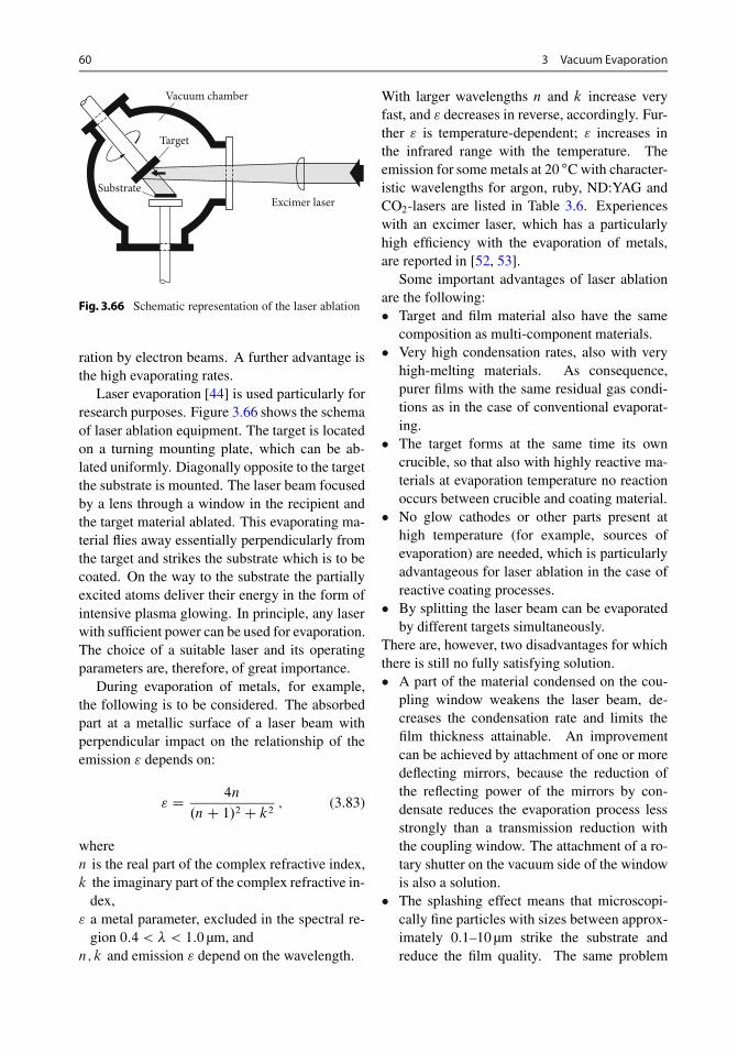
60 3 Vacuum Evaporation
Vacuum chamber
Excimer laserSubstrate
Target
Fig. 3.66 Schematic representation of the laser ablation
ration by electron beams. A further advantage isthe high evaporating rates.
Laser evaporation [44] is used particularly forresearch purposes. Figure 3.66 shows the schemaof laser ablation equipment. The target is locatedon a turning mounting plate, which can be ab-lated uniformly. Diagonally opposite to the targetthe substrate is mounted. The laser beam focusedby a lens through a window in the recipient andthe target material ablated. This evaporating ma-terial flies away essentially perpendicularly fromthe target and strikes the substrate which is to becoated. On the way to the substrate the partiallyexcited atoms deliver their energy in the form ofintensive plasma glowing. In principle, any laserwith sufficient power can be used for evaporation.The choice of a suitable laser and its operatingparameters are, therefore, of great importance.
During evaporation of metals, for example,the following is to be considered. The absorbedpart at a metallic surface of a laser beam withperpendicular impact on the relationship of theemission " depends on:
" D 4n
.nC 1/2 C k2 ; (3.83)
wheren is the real part of the complex refractive index,k the imaginary part of the complex refractive in-
dex," a metal parameter, excluded in the spectral re-
gion 0:4 < � < 1:0 µm, andn; k and emission " depend on the wavelength.
With larger wavelengths n and k increase veryfast, and " decreases in reverse, accordingly. Fur-ther " is temperature-dependent; " increases inthe infrared range with the temperature. Theemission for some metals at 20 ıC with character-istic wavelengths for argon, ruby, ND:YAG andCO2-lasers are listed in Table 3.6. Experienceswith an excimer laser, which has a particularlyhigh efficiency with the evaporation of metals,are reported in [52, 53].
Some important advantages of laser ablationare the following:� Target and film material also have the same
composition as multi-component materials.� Very high condensation rates, also with very
high-melting materials. As consequence,purer films with the same residual gas condi-tions as in the case of conventional evaporat-ing.
� The target forms at the same time its owncrucible, so that also with highly reactive ma-terials at evaporation temperature no reactionoccurs between crucible and coating material.
� No glow cathodes or other parts present athigh temperature (for example, sources ofevaporation) are needed, which is particularlyadvantageous for laser ablation in the case ofreactive coating processes.
� By splitting the laser beam can be evaporatedby different targets simultaneously.
There are, however, two disadvantages for whichthere is still no fully satisfying solution.� A part of the material condensed on the cou-
pling window weakens the laser beam, de-creases the condensation rate and limits thefilm thickness attainable. An improvementcan be achieved by attachment of one or moredeflecting mirrors, because the reduction ofthe reflecting power of the mirrors by con-densate reduces the evaporation process lessstrongly than a transmission reduction withthe coupling window. The attachment of a ro-tary shutter on the vacuum side of the windowis also a solution.
� The splashing effect means that microscopi-cally fine particles with sizes between approx-imately 0.1–10 µm strike the substrate andreduce the film quality. The same problem

3.5 Equipment Technology 61
Table 3.6 Emission of different metals at 20 ıC by some laser wavelengths
Metal
Emission
Ar(500 nm)
Rubin(700 nm)
Nd:YAG(1000 nm)
CO2
(10 µm)
Aluminium 0.09 0.11 0.08 0.019
Cooper 0.56 0.17 0.10 0.015
Gold 0.58 0.07 – 0.017
Iridium 0.36 0.30 0.22 –
Iron 0.68 0.64 – 0.035
Lead 0.38 0.35 0.16 0.045
Molybdenum 0.48 0.48 0.40 0.027
Nickel 0.40 0.32 0.26 0.03
Niobium 0.58 0.50 0.32 0.036
Platinum 0.21 0.15 0.11 0.036
Rhenium 0.47 0.44 0.28 –
Silver 0.05 0.04 0.04 0.014
Tantalum 0.65 0.50 0.18 0.044
Tin 0.20 0.18 0.19 0.034
Titanium 0.48 0.45 0.42 0.08
Tungsten 0.55 0.50 0.41 0.026
Zinc – – 0.16 0.27
also arises with arc evaporation. The densityand size of these particles also decrease withthe energy of the laser beam and with increas-ing distance from the target substrate.
With arc evaporation one must differentiate be-tween anodic and cathode arc evaporation. Cath-ode arc evaporation is based on the followingprinciple. [54, 55].
Along with the current voltage characteristicin a gas discharge obtained within a pressurerange between approximately 10�1–10�3 mbaran abnormal gas discharge adjusts betweena cathode and an opposite anode, which is char-acterized by the fact that with increasing voltagedifference also the current increases.
Further increase of the voltage leads to sparkbreakdown, which is characterized by steeplydropping voltage with increasing current, follow-ing from the range of the arc discharge withcurrent densities of 107–1011 A=m2. Pressure,gas species and electrode configuration influencethe minimum amperage.
The material (cathode) to be evaporated,which can be of different standardized sizes of
a
b
c
d
Fig. 3.67 Schema of a vacuum arc evaporator for ca-thodic evaporation. a anode, b target, c insulator, d watercooling
either circular or rectangular form, situated oppo-site any formed anode between an electrical arc isignited (see Fig. 3.67). The arc feeds on the evap-orating material, so that such an arc discharge canbe operated also under high vacuum conditions.
The arc moves in statistic distribution over thecathode surface, whereby also several spots canoccur at the same time. Due to the high powerdensity of approximately 1011 W=cm2 within therange of the cathode surface (spot), an arc strikesthe cathode material and evaporates it. Within the

62 3 Vacuum Evaporation
range of the spots, which have a diameter of ap-proximately 10 µm, temperatures range between3000 and 6000 K.
Apart from the problem-free evaporation ofalloys – target material and film possess the samecomposition – the high ionization rate of vapourand residual gas for reactive coating processesare also of advantage. With a stabilized magneticfield arc evaporation systems can be manufac-tured, such as Al2O3, AlN, VN, VOx , TiN, ZrO2
and ZrN splash free films.Anodic vacuum arcs [56], which work with
spots on cold cathodes and with evaporating hotanodes, have the advantages of thermal evapora-tion, such as the high evaporation rate, the lowthermal load of the substrates, low operating volt-age with the advantages of a plasma-supportedprocedure such as separation of the films fromthe plasma condition with high adhesion on thesubstrate, and homogeneous films of compactstructure with characteristics close to the respec-tive solids.
A further difference is the different relation-ship of the anode surface to the cathode surface,which is very small in the anodic process (seeFig. 3.68). The evaporation is done via electronbombardment with small currents; the electronshave a low energy and thus a higher probability ofionization than with electron beam evaporation.The ionization rate lies between 0.5 and 10 %.Additional ions develop, which are accelerated,so substrate cleaning by a dry etching process be-fore the beginning of coating is possible.
Theoretical considerations assume that at thebeginning of the process on a small range of theanode, spots form, which lead to heating andevaporation of a small material quantity. Thedeveloping higher density inside these rangescauses an increased energy flow, which thenagain produces more vapour, until finally equi-librium adjusts itself. Discharge is stabilized bythe high temperature of the anode.
Typical operational data from anodic arc evap-orators are:Remainder gas pressure 10�3 to 10�5 mbarArc voltage � 20VCurrent � 20 to 200AEnergy � 0:4 to 4 kW
c
d
ae
b
Fig. 3.68 Schema of a coating equipment with anodic de-position by a vacuum arc evaporator. a anode, b cathode,c substrate stops, d glowing electrode, e evacuation sys-tem
Substrate temperature � 70 ıCDeposition rate 0.1 to 100N m=sElectron temperature 0.4 to 1 eVElectron density 1015 to 1018 m�3
Ion temperature 1 eVIon energy 5 to 150 eVIonization rate of 0.5 to 10 %.
3.6 Ion Plating
3.6.1 Characterization of Ion Plating
Ion plating is a vacuum coating process, by whichthe condensation of vapour takes place under theinfluence of ions within a feed gas or of ionswithin the vapour. The collisions of the ions withthe substrate surface and/or the condensing filmare connected with a transfer of an energy trans-mission and an impulse transmission. These arethe cause for the change of the film characteris-tics by the ion effect at the condensation of thefilm. By the ion plating process the following el-ementary processes take place [57, 58].
At the collision of high-energy ions sputter-ing of the substrate surface and/or the adsorbfilms occurs. If vapour condensation begins,further substrate material sputters, a partial re-sputtering of the condensing material takes place;with progressive condensation only a part of thecondensate is resputtered. In addition, the ions

3.6 Ion Plating 63
produce a certain defect concentration, wherebythe surface is activated.
The influence of the ions on the film propertiesdetermines to which extent the energy balanceis changed with the condensation. The energytransfer is connected with the condensing vapourstream,
ED D nD � eD ; (3.84)
wherenD are the number of condensing neutral vapour
particles for each time and unit area, andeD their mean kinetic energy.eD is approximately
eD D 3
2kTV ; (3.85)
wherek is the Boltzmann constant, andTv the evaporation temperature.The energy transfer by the striking ions is
EI D nI eI ; (3.86)
wherenI is the number of the ions is for each time and
unit area, andeI the middle energy of an ion.To this applies
eI D e UI ; (3.87)
where U I is the middle accelerating voltage ofthe ions. An indicator for the energetic activationof the substrate surface is the energy relation-ship [58]
"I D EI CED
ED: (3.88)
The energy relationship denotes the factor bywhich the condensation energy is increasedthrough the influence of the ions in relation to thecondensation energy by evaporation. As long ashas not yet led to a rise in temperature of the sub-strate due to transients, the energetic excitationof the surface atoms corresponds to a higher ef-fective condensation temperature TK, as it arisesfrom the middle substrate temperature TS [57].Among other things, a larger mobility of thecondensing particles and thus a higher rate of dif-fusion velocity result.
Since generally ED � EI, the energy rela-tionship approaches the rate relationship nI=nD
of ions and vapour particles at the substrate sur-face. The middle accelerating voltage of the ionsis, therefore,
"I � 6 � 103 UI
TV� nI
nDI (3.89)
UI in V ; TV in K :
A characteristic value for the middle energy "D ofa vapour particle at an evaporation temperature ofapproximately 2000 K is 0:2 eV. Typical valuesfor the middle energy "D of the ions at the ionplating are 50–5000 eV.
Table 3.7 shows different values of the rela-tionship nI=nD and the size U I. With ions ofU I D 500V, for example, with a small raterelationship nI=nD � 3 � 10�3, an energeticactivation can be reached, which corresponds toenergy conditions at sputtering. By the choice ofU I, in particular, by change of the relationshipnI=nD, the energy relationship can be varied byorders of magnitude. Because of the different de-pendence of the elementary effects on the numberof the ions and the ion energy, generally the ionplating effects differ with the same "I value. Inorder to achieve high values for "I, ionization fa-cilities must be used for ion plating, with whichlarge values for nI=nD can be carried out [59].
Ion plating is limited by an increase of resput-tering and by an increase of the temperature ofthe substrates.
An important condition for the guidance ofthe ion plating process is that the condensationrate aK must exceed the resputtering rate aS,
aS
aK< 1 : (3.90)
aK is the condensation rate, which would resultin the case of evaporation without ion effect. Forthis reason, the relationship of the energy rela-tionship "I with the rate relationship is aS=aK isof interest. With a simplifying assumption ap-plied in a reduced range, the accelerating voltagefor the ions and/or the discharge voltage UB ofthe ionization facility,
"I D KpUBaS
aK: (3.91)

64 3 Vacuum Evaporation
Table 3.7 Energy relationship "I at the ion plating to the comparison by evaporation and sputtering
Technology of deposition "I Parameter
High vacuum evaporation 1 eD D 0:2 eV
Sputtering 5–10 eS D 1–2 eV
Ion plating
1.2nlnD
Ul in V
10�3 50
3.510�2 500
10�4 5000
2510�1 50
10�3 5000
25010�1 500
10�2 5000
2500 10�1 5000
nI=nD relationship of the number of the ions to the number of the vapour particles; U I average accelerating voltage ofthe ions; eD average energy of a vapour particle; eS average energy of a sputtered particle.
3.6.2 Influence on the FilmCharacteristicsand Consequencesfor the Coating Process
From the mechanism of the ion plating processit follows that between vapour, ions and gas act-ing elementary processes create more complexcondensation conditions than evaporation. Adhe-sion mechanisms influence the development andgrowth of nucleation and the morphology of thefilm in a particular orientation and structure; inaddition, stoichiometry and surface topographycan be modified with the ion plating.
These physical and partial chemical effectsmodify the film properties of evaporated films.The sputtering of adsorption films that cover thesubstrate surface, the creation of mixed interfacefilms from sputtered substrate and film mate-rial, the diffusion of both materials, the higherbinding energy of activated centres [57] and thechanged adhesion coefficient ionized vapour pro-duce ion plated films with good adhesion [49].Large adhesion is a condition for application ofvery thick films.
Ion bombardment during the condensation ofthe film, in situ cleaning, can lead to increasedpurity of the film. Resputtering and gas adsorp-tion can be a frequent cause for a larger seed filmdensity and thus for finer granular film structure.The energetic excitation, of which resputtering
and gas adsorption can cause a change of thenature of the growth, for example change of theorientation of crystals, and a transition of pillaredto isotropic or equiaxial growth [53] at substratetemperatures, at which this growth is normallynot possible [51]. Under the influence of ionsrecrystallization at room temperature was ob-served. An increased binding energy of activatedcentres and changed adhesion coefficients of ion-ized gas are causes of increased gas content inthe film and selective insertion of alloy compo-nents. In this way the implantation of unsolvablecomponents can be achieved, for example heliumin gold [52] or phosphorus and lithium in zincselenide. Scattering in the gas and the differ-entiated resputtering, particularly at cupids andedges as a consequence of the electrical fieldgradient, are the cause for the high degree ofcoverage [53] and small porosity [48]. The useof an ionization system at the start and duringthe evaporation permits inclusion of sputteringto clean the substrate and in situ cleaning of thefilm into the coating process.
3.6.3 Equipment for Ion Plating
There are many different possibilities of pro-ducing vapour and ions and accordingly diversesystems have been developed [65].

3.6 Ion Plating 65
Negative potential
Substrate
Gas dischargeplasma
Vapour flowThrotteling ofthe pumping
speed
Throttling ofthe pumping
speed
Axial gunwith 90° deflection
Flow resistance (pipe)
Flow resistance(aperture)
Gas inletvalve
Adapter for thehigh vacuum
generator
Dividing wall inthe recipient
Adapter for thehigh vacuum
generatorTransverse evaporator
Gas inlet valve
pG < 10–2Pa
10–1...1Pa 10–1...1Pa
pG < 10–2Pa
ba
Fig. 3.69 Schematic representation from systems for ion plating with electron beam evaporator and direct current gasdischarge between evaporators and substrate, a with axial gun, b with transverse gun
In order for ion plating to reach high coatingrates, electron beam evaporators [66] are used forthe evaporation. In the simplest systems the elec-tron beam is used as the energy source for theproduction of the vapour stream and also for ion-ization of the vapour stream.
Vapour ions produced by a primary electronbeam within the range of the crucible are suckedup by a negative current of some thousand voltsand accelerated to the substrate.
With such an arrangement the ion current den-sity reached on the substrate is too small fortechnical applications. A cause for the low ioncurrent is the low ionization probability of vapourparticles by fast ions with energies in the order of10�30 keV.
An advantage of this solution is that the pro-cess can be implemented in high vacuum, ata pressure by 10�4 mbar. A possibility for ionplating in high vacuum consists of using the elec-tron beam evaporator only for vapour generationand a separate ion gun for both producing and di-recting the ion beam toward the substrate. Thisarrangement permits us control the ion currentand the vapour stream separately; however, tocontrol the ion beam is complex.
Usually, a system is used that consists ofan electron beam evaporator for vapour genera-tion and a direct current gas discharge betweenevaporators and substrate for the production ofa current of vapour and feed gas ions. Sourcesof ionization are both the electron beam andthe plasma, which are formed between the elec-trodes for discharge. Figure 3.69 shows thearrangements for electron beam evaporators witha transverse gun and an axial gun.
If the ion plating takes place with a feed gaspressure from 1–7 � 10�2 mbar, then a pressuregradient of 100 : 1 is necessary. With the applica-tion of self-consistent gas discharges with a cur-rent density within the range around 1mA=cm2
and high evaporation rates only small values ofthe relationship are possible for nI=nD. An in-crease of the ion current density, in particular ofvapour ions, is reached by arrangement of thecrucible in an axial magnetic field. This wayslow secondary electrons can be used for addi-tional ionization. Ionization of vapour and/orthe feed gas can be also be achieved with highfrequency [25]. Such an arrangement makesion plating possible for non-conductive sub-strates. The use of a planar plasmatron, a circular

66 3 Vacuum Evaporation
aV
aS
aV
aS
aS
aV
EvaporatorMoved band or moved plate over a large evaporator
Band-shaped substrate Ionization device
c
Rotatable basket with a source of vapor and agas discharge on the entire extent
b
Rotatable basket with a source of vapor and a ionization equipment
avapourparticle
Evaporator
Melting
Ionizationdevice
Ion
Rotatable basketSubstrate
Fig. 3.70 Examples of possible arrangements of the alternating ion plating and timeline of the evaporation rate and theresputtering rate aS for each substrate place (schematic)
gap discharge system for ion plating [59], per-mits production from ion current densities over100mA=cm2.
In combination with movement mechanismsfor the substrates, however, this process makesthe application of ion plating for coating largesurfaces with a high rate possible. Moreover,with respect to the discharge pressure and thusthe pressure at the coating process, this type ofdischarge is very flexible.
On the one hand, amperage discharge is stillpossible in the pressure range of 5 � 10�4 mbarpossible, and on the other hand, this disposi-tion qualifies within the pressure range of thegas scattering coating, i.e. up to 10 mbar is suit-able. Figure 3.70 shows a plant for alternatingion plating with an electron beam evaporator withflow resistance; an ionization facility of the pla-nar plasmatron type and a rotary disc substratemounting plate [59].
3.6.4 Structural Constitution of the IonPlated Films
The structural constitution and the physical char-acteristics of the future film, the substrate tem-peratures, the condensation rate, and the pressureof the surrounding gas atmosphere determine, ifnecessary the relationship of the partial pressureof the gas mixtures and the energy of the ions andneutral particles.
During cathode sputtering with negativelybiased substrate the energy of these particlesis at some ten eV, with ion plating witha gas discharge energies up to some hundredseVoccur [67]. Due to these comparatively highenergies in an interface film (transition region) itcan come to implantation of high energy particlesfrom the gaseous phase and recoil implantationof surface atoms; a procedure that is described asphysical mixing or pseudo diffusion.

3.6 Ion Plating 67
For film growth, and thus for the quality ofthe film, the mobility of the condensing parti-cles at the film surface essentially depends on thesubstrate temperature and the energy of the arriv-ing particles. Aspired is a compact, glass-like ornanocrystalline structure of the film with no in-side stress and high adherence.
The correlation between the structural condi-tion of the film and the process parameters isrepresented in structured models. B.A. Movchanand A.V. Demchishin [68] derived a three-zonemodel from structure investigations on the ba-sis on thick vapour-deposited nickel, titanium,tungsten-aluminium oxide and zircon oxide. Thisis shown in Fig. 3.71a. An independent variableis the relationship T=TM, where T is the sub-strate temperature during the condensation andTM is the melting temperature of the coatingmaterial. The introduction of the melting tem-perature here is meaningful, because the bindingenergy between the condensing particles of thissize is proportional to TM.
Is the relationship smaller with metals than0.26 (0.3 by chemical compounds), then theadsorbed atoms have less mobility on the sur-face, shadowing effects can become unbalanced,and a porous dendritically structure from needle-shaped crystals with round end shaped ends(zone 1) results to zone 2, which is charac-terized from a closely packed stack structure(columnar structure) with a surface of smallroughness, which has a developing higher mo-bility of the adsorbed atoms within the range0:26 T=TM 0:45. Volume diffusion leads tozone 3 with a recrystallized film, high componentdensity and smooth surface film.
The three-zone model for vapour-depositedfilms was extended by J.A. Thornton [69] for upto 25 µm films of metal (Mo, Co, Ti, Fe, Cu andaluminium alloys) created with cathodic sputter-ing in argon, (Fig. 3.71b). Impacting particles onthe substrate surface have a substantially higherenergy (about 4–40 eV) than with by evapora-tion (0.1–0.2 eV). They also depend on the gaspressure because the particles coming from thecathode lose energy when the particles impactwith the gas particles by crossing the dischargearea. The higher the gas pressure, the smaller
a
b
Zone 1
Metals < 0.26 0.26 ... 0.45 > 0.45Oxides < 0.26 0.26 ... 0.45 > 0.45
Zone 2 Zone 3
Zone 1
Zone 2 Zone 3
Zone T
302010–3
10
1 0.10.2
0.30.4
0.50.6
0.70.8
0.91.0
mbarp T/Tm
Fig. 3.71 Structured models. a according to B.A. Mov-chan and A.V. Demchishin [68], b after J.A. Thorn-ton [69]. T D substrate temperature, Tm D meltingtemperature
the average kinetic energy of the condensing par-ticles and thus their mobility on the substratesurface. Below T=TM 0:5, with removingpressure we have a more broadly transition re-gion T, which exhibits a close fibrous structurewith a smooth surface.
The growing film is exposed to a constantbombardment with particles of high energy,which increases the mobility of the adsorbedatoms. This particularly applies during cathodicsputtering with a negatively biased substrate.Therefore, it is more meaningful to represent thestructural constituent as a function of the entireenergy reaching the surface [59]. This is shownin Fig. 3.72a for sputtered germanium films. Asthe schematic representation shows, the limit be-tween zones 1 and T shifts to lower temperatureswith increasing energy.
A further structural model [59] is shown inFig. 3.72 for a higher energy region (200–500 eV)of the impacted ions, as is typical for ion plating

68 3 Vacuum Evaporation
Zone T
00.1
0.50.4
0.30.2
0.6
T/Tm
T/Tm
Zone 1
Zone 2
Zone 2 c -Ge
a -Ge
23
Zone 3
Zone 3
550500
400300
250W
W
0.100.2 0.30.4
0.50.6
0.7 0.80.91.0
a
b
~ 100eV
Fig. 3.72 Structure models. a after R. Messier et al. [70],b after C. Fountzoulas and W.B. Nowak [65]. T D sub-strate temperature, Tm D melting temperature, W D ionenergy
with gas discharge. The structural constituent ofgermanium films (thickness about 1.5 µm, a con-densation rate of about 0.4 µm=min) as a functionof the total energy measured in the contrary fieldof particles striking the substrate is shown in thefigure. It is remarkable that there is an absence ofzones 1 and T and that there is a tightly packedfilm structure of zone 3 at room temperature.T=TM D 0:25/ and high ion energy .� 500 eV/.
3.6.5 Adhesive Strengthof Ion Plated Films
The basic condition for the usefulness of ionplated films is a high adhesive strength, whichdepends on the internal stress of the depositedfilm. At all coating processes stress in the filmcan occur if the atoms are prevented to take onthe state of deepest energy at the growth of thefilm. Disturbances of the equilibrium are caused
by gas incorporation and the formation of defectstructures; they are inevitable at typical manufac-ture conditions of the ion plated films. On theother hand, if by the choice of the process param-eters, in particular the ion energy, the film growthcan be controlled in such a way that closelypacked structures develop, which offer variouspossibilities such as volume diffusion and recrys-tallization to stress compensation.
Ion plated films, that have been manufacturedunder accordingly adjusted conditions, show sub-stantially improved adhesion conditions, alsowith large film thicknesses as compared to evap-orated films (10–100 µm) and material combina-tions, from which one would not expect goodadhesion. Thus, ion plated silver films of 12 to50 µm thickness were applied on stainless steelwith an adhesive strength of 300N=mm2 [72].
Ion-plated films can withstand even the ex-treme demands during cold massive forming.A thick copper film with MoSi2-lubrication lac-quer on titanium proved to be an optimal in-termediate film to avoid cold welding with cupreverse extrusions with a deformation up to 92 %a 1.3 µm.
Electron microscope pictures show that ionplated copper films cover titanium even after adeformation of 400 % of the coherently coveredsurface [71].
3.6.6 Reactive Ion Plating
Reactive ion plating designates ion plating pro-cesses that operate in the presence of reactivegases (for example, O2, N2, C2H2/.
Oxides, nitrides, carbides, etc. need to developsubstrate temperatures around 400 ıC; normallytemperatures between 800 and 1000 ıC are nec-essary.
Titanium nitride films are frequently used, de-pending upon process conditions, in differentphases (TiN and Ti2N) and different crystal ori-entations. Depending on the process parameters,the films have different structural conditions andharnesses between 2000 and 3000 HV [73]. Withthe production of titanium nitride films the N2
partial pressure is critical. By variation of the
3.6 References 69
manufacturing parameters titanium nitride filmsof different forms can be manufactured, as theyare used for decorative purposes.
References
1. Mattox DM (2010) Handbook of Physical Vapor De-position (PVD) Processing, 2nd edn. William Andrew
2. Cho JA (1971) Film Deposition by Molecular BeamTechniques. J Vac Sci Tech 8:S31–S38
3. Cho JA (1975) Molecular Beam Epitaxy. Prog Solid-State Chem 10:157–192
4. Sacks R, Sieg R, Ringel S (1996) Investigation of theAccuracy of Pyrometric Interferometry in Determin-ing AlxGa1�xAs Growth Rates and Compositions. JVac Sci Tech B 12(3):2157–2162
5. Pinsukanjana P, Jackson A, Tofte J, Maranowski K,Campbell S, English J, Chalmers S, Coldren L, Gos-sard A (1996) Real-time Simultaneous Optical-BasedFlux Monitoring of Al, Ga, and In using Atomic Ab-sorption for Molecular Beam Epitaxy. J Vac Sci TechB 14(3):2147–2150
6. Williams JS, Poate JM (eds) (1984) Ion Implantationand Beam Processing. Academic Press
7. Ziegler F (2000) Ion Implantation Science and Tech-nology. Edgewater, USA
8. Hilleringmann U (2004) Silizium-Halbleitertechnolo-gie. Teubner
9. Frey H (1992) Ionenstrahlgestützte Halbleitertech-nologie. VDI-Verlag, Düsseldorf
10. Marshall A, Natarajan S (2002) SOI Design: Analog,Memory and Digital Techniques. Springer
11. Burrows G (1965) Evaporation in an evacuated con-tainer. Vacuum 15(8):289–399
12. Langmuir J (1973) The vapour pressure of metallictungsten. Phys Rev 2(5):329–342
13. Movcan BA, Domcisin AV, Kulak LD (1974) Struc-ture and mechanical properties of thick Fe, Fe-NbC,Fe-Ni-NbC- condensates. J Vac Sci Technol 11:869–874
14. Schiller S et al (1967) Erfahrungen mit einem5 kW Elektronenstrahlverdampfer. Vakuum-Technik16(167/ 9):205–209
15. Taylor RC (1974) Single source evaporation ofgadolinium cobalt alloys. J Vac Sci Technol11(6):1148–1150
16. Oron M, Adams CM (1969) Controlled electron beamco-deposition of copper-nickel films. J Mater Sci4(169):252–258
17. Swift RA, Noval BA, Merz KM (1968) Fractionationof Ni-Cr-Cu-Al alloys during vacuum evaporation. JVac Sci Technol 5(3):79–83
18. Santala T, Adams CM (1970) Kinetics and thermo-dynamics in continuous electron-beam evaporation ofbinary alloys. J Vac Sci Technol 7(6):22–29
19. Forster JS, Pfeifer WH (1972) Vacuum deposition ofalloys – theoretical and practical considerations. J VacSci Technol 9(6):1379–1384
20. Andreini RJ, Forster JS (1974) Kinetics of solute re-moval during electron-beam and vacuum-arc melting.J Vac Sci Technol 11(6):1055–1059
21. Hulgren C et al (1963) Selected Values of Thermo-dynamic Properties of Metals and Alloys. J. Wiley &Sons Inc., New York, p 732
22. Wagner C (1962) Thermodynamics of Alloys.Addision-Wesley, Reading, Mass., pp 15–17
23. Olette M (1960) Élemination sous vide des oligo-élémentes contenus dans les alliages ferreux. MemSci Rev Met 67(6):467–480
24. Richards JL (1966) Flash-evaporation. In: AndersonJC (ed) The Use of Thin Films in Physical Investiga-tions. Academic Press, New York, pp 71–85
25. Harker HR, Hill RJ (1972) The deposition of multi-component phases by ion plating. J Vac Sci Technol9(6):1365–1399
26. Smith HR, Kennedy K, Boericke FS (1970) Metallur-gical characteristics of titanium-alloy foil prepared byelectron beam evaporation. J Vac Sc Technol 7(6):48–51
27. Krutenat RC (1974) Effect of pool temperature gra-dients on the compositions of electron beam vapourdeposited alloys. J Vac Sci Technol 11(6):1123
28. Stowell WR (1973) Single source evaporation of aniobium based alloy containing volatile constituents.J Vac Sci Technol 10(4):489–493
29. Hoffmann D, Leibowitz D (1971) Al2O3 Films pre-pared by electron beam evaporation of hot pressedAl2O3 in oxygen ambient. J Vac Sci Technol8(1):107–111
30. Hoffmann D, Leibowitz D (1972) Effect of substratepotential on Al2O3 films prepared by electron beamevaporation. J Vac Sci Technol 9(1):326–329
31. Bunshab RF, Raghuran AC (1972) Activated reactiveevaporation process for high rate deposition of com-pounds. J Vac Sci Technol 9(6):1385–1388
32. Stowell WR (1974) Ion-plated titanium carbide coat-ings. Thin Solid Films 22(1):111–120
33. Mattox DM (1973) Thin film metallization of oxidesin microelectronics. Thin Solid Films 18(2):173–186
34. Heitmann E (1972) Reaktives Aufdampfen in reak-tiven Gasen. Vakuum-Technik 21(1):1–11
35. Ramprasad BS, Rhada TS (1974) Optimum geome-try for uniform deposits on a rotating substrates froma pint source Vacuum 24, 4, p. 165

70 3 Vacuum Evaporation
36. Graper EB (1973) Distribution and apparent sourcegeometrie of electron-beam-broad evaporationsources. J Vac Sci Technol 10(1):100–103
37. Turner ME (1973) How to specify the right source tothe right job. Solid State Technol 16(7):16–18
38. Soa EA, Persch G (1974) Die Dicke der Aufdampf-schichten in ihrer Abhängigkeit von technischen Pa-rametern. Exp Techn Phys 22(6):571–583
39. Erikson (1974) E.D.: Thickness distribution of a met-all – alloy from a high-rate electron beam source. JVac Sci Technol 11(1):366–370
40. Mulder BJ (1977) A method for the splash-free evap-oration of the aluminium and other metals. Vacuum28(1):11–12
41. Kirner K (1970) Reaktionen beim Verdampfen vonAluminium in Bornitridtiegeln, CVA, pp. 64/65
42. Parent ED (1974) Power requirements of resistance-heated intermetallic evaporation sources. J Vac SciTechnol 11(4):820–822
43. Dobrowolzki JA (1977) Source configurations for thedeposition of uniform thin films onto a moving web.In: Proc. 7th Intern. Vac. Congr. & 3rd Intern. Conf.Solid Surfaces Vienna, pp 1567–1570
44. Reuter W (1976) Optimierung der Verdampfera-nordnung bei Bandbedampfungsanlagen. Maschinen-markt, Würzburg 82(81):1479–1482
45. Warren KA, Denison PR, Bills DG (1967) Resistanceheated sublimator. The Review of Scientific Instru-ments 38(8):1019–1022
46. Morley JR, Smith HR (1972) High rate ion productionfor vacuum deposition. J Vac Sci Technol 9(6):1377–1378
47. Burlirsch R, Stoor J (1966) Numerical treatment ofordinary differential equations by extrapolation meth-ods. Numer Math 8:1–13
48. Schiller S et al (1967) Erfahrungen mit einem5-kW Elektronenstrahlverdampfer. Vakuum-Technik16(9):205–209
49. Hill F (1974) Evaporated aluminium films; A re-view of techniques and recent improvements. AircoTemescal, Berkley, Calif
50. Schiller S et al (1974) Industrial electron beam coat-ing of trip steel. In: Silva RM, Electron Beam Pro-cessing Seminar Stratford-upon-Avon, pp. 2d1–2d28
51. Groeschl ME, Benes E, Schmidt E, Siegmund H,Thorn G, Thomas FW (1989) Sensor for the detec-tion of the incident point of an electron beam. ThinSolid Films 174:323–329
52. Scheibe H, Gorbunov AA, Baranova GK, KlassenNV, Konov VI, Kulakov MP, Prokhorov AM, Weis HJ(1990) Thin Film Deposition by Eximer Laser Evap-oration. Thin Solid Films 189:283–291
53. Coutal C, Azema A, Roustan JC (1996) Thin SolidFilms. Elsevier
54. Barth KL, Lunk A, Ulmer J (1997) Surface and Coat-ings Technology. Elsevier
55. Rother BJ, Siegel J, Vetter J (1990) Cathodic ArcEvaporation of Graphite with Controlled CathodeSpot Position. Thin Solid Films 188:293–300
56. Ehrlich H, Hasse B, Mausbach M, Müller KG (1990)The anodic vacuum arc and ist application to coating.J Vac Sci Technol A 8(3):2160–2164
57. Mattox DM (1973) Fundamentals of ion plating. J VacTechnol 10(1):47–52
58. Schwan J, Ulrich S, Roth H, Ehrhardt H (1996) Tetra-hedral amorphous carbon films prepared by mag-netron sputtering and dc ion plating. Journal of Ap-plied Physics 79:1416–1422
59. Schiller S, Heisig U, Goedicke K (1975) Alternatingion plating – a way to high rate ion vapour deposition.J Vac Sci Technol 12(4):858–864
60. McLeod PS, Mah G (1974) The effect of substratebias voltage on the bonding of vaporated silver coat-ings. J Vac Sci Technol 11(1):119–121
61. Boone DH, Strangman TE, Wilson LW (1974) Someeffects of structure and composition on the propertiesof electron beam vapour deposited coating for gas tur-bine superalloys. J Vac Sci Technol 11(4):641–646
62. Bunshah RF (1974) Structure property relationshipsin evaporated thick films and bulk coatings. J Vac SciTechnol 11(4):633–638
63. Berg RS, Kominiak GJ, Mattox DM (1974) Incorper-ation and behaviour of helium in ion deposited Films.J Vac Sci Technol 11(1):52–55
64. Jouan PY, Lempérière G (1991) Ion energy distribu-tion at a negatively based electrode in a sputteringdischarge. Vacuum 42:927–931
65. McNally JJ (1990) Ion assisted deposition Handbookof Plasma Processing Technology. Noyes Publica-tions, pp 466–482
66. Chambers DL, Cermichael DC (1971) Electronbeam techniques for ion plating. Res And Develop22(5):32–35
67. Ion assisted deposition Handbook of Plasma Process-ing Technology Noyes Publications (1990) pp. 466–482
68. Movchan BA, Demchishin AV (1969) Study of thestructure and properties to thick vacuum condensatesof nickel, titanium, tungsten, aluminium oxide andzirconium dioxide. Fiz Metal Metallowed 28:653–660
69. Thornton JA (1974) Influence of apparatus geome-try and despositions conditions on the structure andtopography of thick sputtered coatings. J Vac SciTechnol 11:666–670
70. Merssier R, Giri AP, Roy RA (1984) Revised structurezone model for thin film physical structure. J Vac SciTechnol A 2:500–503

3.6 References 71
71. McNally JJ (1990) Ion assisted deposition Handbookof Plasma Processing Technology. Noyes Publica-tions, pp 466–482
72. Riebeling I, Thoma K, Gärtner H (1985) Ion platingof copper layers on titanum: influence of preparationparameters and deformation on the residual stresses.Mater Sci Eng 69:435–444
73. Matthews A (1985) Surface Engineering 6:93–104

4Basic Principle of Plasma PhysicsH. Frey
4.1 Introduction
Thin film technologies are generally based onplasma-supported methods (see Fig. 4.1).
Plasma means:� When in a liquid or a gas the number of free
charge carriers is so large that charge carriersaffect the physical properties of the mediumsubstantially.
� When electromagnetic interactions betweenthe charged particles take place.
� When the number of positive and negativecharge carriers is for each unit of volumeequally large in each case; the total quantitycan be arbitrary.
The number of existing neutral particles (atoms,molecules) is not relevant for the definition ofplasma. Since plasma contains free charge car-riers, it is current conducting. Electric cur-rents produce magnetic fields and so electri-cally charged particles by electrical and magneticfields can be influenced, also a plasma can beinfluenced by external electrical and magneticfields. Furthermore the plasma produces suchfields and, therefore, the plasma can take in in-teraction with itself. In electrodynamics plasmais generally an anisotropic, non-linear disperserconductor, i.e. the energy for plasma excita-tion can be supplied by means of electromagneticfields of different frequency.
4.2 Quasi-Neutrality
A plasma is not electrically charged, because itcontains free charge carriers. From the outsideit is electrically neutral, since on the average thenumber of positive and negative charge carriers isequally high for each unit volume. Powerful elec-trical fields maintain this electrical equilibrium,the quasi-neutrality [1].
If electrons ne are contained in a cubiccentimetre, then the total charge contained ina sphere of the radius r is
Q D �4�4�3"0
r3nee ; (4.1)
where e is the elementary charge and "0 the elec-trical field constant.
If we assume a central symmetrical distribu-tion of the electrons, then we can represent thewhole chargeQ in the centre of the sphere. In thedistance r from the average value of the spherethis charge produces an electrical field of thestrength
E D Q
r2: (4.2)
If we select r D 1 and ne D 1015 cm�3, we ob-tain E D 6 � 108 V=cm. In the condition ofquasi-neutrality, however, the positive and neg-ative charges are equal for each unit volume.When ni is the number of ions and CZe thecharge of the Z-fold positively charged ions, thecondition of quasi-neutrality is:
ne D Zni (4.3)
73© Springer-Verlag Berlin Heidelberg 2015H. Frey, H. R. Khan, Handbook of Thin-Film Technology, DOI 10.1007/978-3-642-05430-3_4

74 4 Basic Principle of Plasma Physics
2 Plasma-CVD
Temperature: 300°C; 500...700°CPressure: 10–3Pa; 10...1000Pa
Energy: HF, DC pulsed
Medium: N2 H2 Ar CH4 TiCl4
Layer: 1...10μmTiN; TiC; i: C
Low temperature of workpiece
Vacuum processElectrical plasma excitation
Medium:gases and vapours
C-H PolymersLayer: 1...100μm
Medium: CxHx-monomer
Temperature: 20...100°CPressure: 1...100Pa
Energy: HF
1 Plas
ma d
iffus
ion
Tem
pera
ture:
300°
C; 500
...800
°C
Pres
sure:
10...1
000P
a
Ener
gy: D
C, DC pu
lsed
Med
ium
: N2
H2
Ar
CH 4 3 PVD
Temperature: 100...500°C
Pressure: 0,01...1Pa
Energy: HF, DC
Medium
: N2 H
2 CH4 C
2 H2 M
etal-
vapours
Layer: 1...10μm
TiN; TiC
6 plas
ma e
tchin
g
Med
ium
: H2
Ar
H2
Tem
pera
ture:
20...2
00°C
Pres
sure:
0,1..
.100P
a
Ener
gy: H
F, DC
Medium
: H2 Ar
Temperature: 20...200°C
Pressure: 10 –3...10 -7Pa
Energy: DC
4 Ion implantation
5 Plasma polymerization
Abra
sion
0,01..
.100μ
mN; C-inclusion
Layer: ≤1μm
Laye
r: 10
0...60
0μm
1...20
μmFe
N; CrN
; AIN
N -, C
-Diff
.
Fig. 4.1 Plasma-supported thin film technologies
orjne D Znij � ne : (4.4)
Since the ions generate a field with E D C6 �108 V=cm, the entire electrical field strength iszero in the condition of quasi-neutrality. If,however, – for example by statistic density vari-ations – it comes only in the relationship 1 : 10�6to a variation from Eq. (4.3), then the electri-cal equilibrium is again reconstituted, generatingelectrical field strength in the amount of 10�6 �6 � 108 D 600V=cm.
This strong field reconstitutes the quasi-neutrality immediately. It is only with the oc-currence of very high frequency oscillations (for
example, of displacement currents) that the ionswith their large mass ca no longer follow, and itcomes to a spatial separation of the centre of massof the positive and negative charge clouds.
The oscillating frequency !0, up to which thedisplacement current can be neglected, is deter-mined by the relationship:
displacement current
conduction currentD "0
@E@t
j� "0!0
< 1 :
(4.5)Here, j is the conduction current density, E theelectrical field strength and the electrical con-ductivity. With an electrical conductivity of the

4.3 Characteristic Quantities 75
plasma at 100��1 m�1 we obtain !0 > 1013 s�1(� D 3 � 10�5 m).
4.3 Characteristic Quantities
4.3.1 Langmuir Plasma Frequency
The force �eE, which an electron repulses intothe volume (attractive force), is harmonic, i.e.proportionally to the deflection from the rest po-sition [2]; it is
� eE D �eQr2D �e2 1
3r3ne
1
r2D �1
3nee
2r ;
(4.6)with the linear (radial) equation of motion (usu-ally linear differential equation of second orderwith constant coefficients), and we obtain
medr2
dtD � 1
3"0nee
2r ; (4.7)
whereme is the electron mass.With the approximated e-potential
r.t/ D r0ei!t ; (4.8)
it follows that the electrons are harmoniously os-cillated with the frequency
! D�nee
2
3me"0
� 12
: (4.9)
With the more exact three-dimensional calcula-tion we obtain the equation
!PI D�nee
2
me"0
� 12
: (4.10)
All these equations are valid only for cold elec-trons (Te D 0K). If the electrons still havethermal motion, then the conditions are morecomplicated.
4.3.2 Debye Shielding Length
If the plasma is considered on the whole as quasi-neutral, this does not exclude that within the
microscopic range electrical fields result fromfluctuations of the charge carrier density. If oneregards the direct environment of an ion, then be-cause they are released by the attractive Coulombforce, more electrons remain on the average here,as this corresponds to the medium density of theelectrons.
Contrarily, other positively charged particlesare kept away due to the repulsive force from thisrange.
In order to be able to calculate the Coulombpotential in the direct environment of such a testparticle, we must use some simplifying assump-tions.� The electrons possess a Maxwell distribution
with the temperature Te.� Due to the thermal movement of the elec-
trons electrical microfields can develop in theplasma, in which the electrons attain potentialenergy. This energy e' should be substan-tially smaller than the thermal energy, i.e.e' � kTe (' potential).
� The positively charged ions are to be uni-formly distributed over the plasma. Theirdensity is everywhere ni D ne0, whereas ne0
is the mean density of the electrons.In a potential field the electron density varies ac-cording to the Boltzmann distribution:
ne D ne0ee'
kTe : (4.11)
Since e' � kTe is, we can also write
ne D ne0
�1 � e'
kTe
�: (4.12)
Over the considered volume average ' disap-pears, since it is developed only by fluctuation,i.e. by space charge fluctuations. The potentialfield ' must be sufficient in the environment ofthe considered position of the Poisson equation.
With E D �Vj (see Sect. 4.4.1) and with con-sideration of Eq. (4.12), we obtain:
��' D e
"0.ne � ni/ D �e
2
"0ne0
'
kTe: (4.13)
With the abbreviation (�D is the Debye length)
�D2 D "0Te=e2ne0 (4.14)

76 4 Basic Principle of Plasma Physics
we sustain�'
'
�2D: (4.15)
Since the potential in the environment of a testparticle is to be considered, this is a sphericallysymmetric problem. We can therefore write:
1
r2d
drr2
d'
drD '
�2D: (4.16)
The limiting values is ' ! 0, if r ! 1, and' ! 'coulomb, if r � ��.
Equation (4.16) is solved with the approach
' D c
re
�rb : (4.17)
Introducing Eq. (4.17) in Eq. (4.16), we imme-diately obtain b D �D; the ansatz thereby fulfilsthe first boundary condition. The constant c isdetermined by the transition of many small r (ascompared to the ion radius). Since � is usuallylarge against the ion radius, it is possible to de-velop the exponential function of the Eq. (4.17):
D c
re
�r�D D c
r
�1 � r
�D
�Š c
rD e
4�"0r:
(4.18)From this it follows that:
c Š e
4�"0(4.19)
or' D e
4�"0re
�r�D : (4.20)
These considerations show that the potential ofa test particle in plasma is correlated by the factorer=�D to the modified Coulomb potential. In thedistance r D �D, the undisturbed coulomb po-tential is already dropped down to an eth of theexponential function part. The electrons, whichaccumulate around an ion, shield the potentialoutwards.
The number of electrons in a sphere aroundthe test particle with the plasma length �D as aradius of the Debye sphere is:
neD D 4�
3�3Dne0 D 4�
3
�"0kTe
ne0e2
� 32
ne0
D 4�
3
�"0kTe
e2
� 32 1
n12
e0
; (4.21)
or, if we summarize the constant factors:
nc D 1:38 � 103 T32
e
n12
e0
: (4.22)
The equation becomes invalid, if the number ofparticles in a Debye sphere becomes lp 1. Wemust use then quantum-mechanical methods.
4.3.3 Landau Length and PlasmaParameters
The distance of a charge in which the electro-static energy in the vacuum is equal to the kineticenergy kT is called the critical distance or theLandau length [3]:
lL D e2
kT 4�"0: (4.23)
If no recombination (Sect. 4.5.4.2 compares) ofelectrons and ions takes place, then the mean dis-tance between plasma particles must be largerthan the Landau length;
˛ > lL : (4.24)
Since the range of influence is given to the elec-trostatic interaction effect by �D, we can write:
˛ > �D ; (4.25)
This means that it does not come to any interac-tion between the plasma particles; this is a swarmof particles that is independent from each other;they are not interacting particles. This is nota plasma.
The Debye sphere (c.f Sect. 4.3.2) contains4�=3�3Dne0 electrons. So we can write:
4�=3�3Dne0 � 1
or
� D 1
ne0�3D
� 1 (4.26)
or
n� 1
3
e0 � �D : (4.27)

4.4 Motion of Charged Particles in Electromagnetic Fields 77
4.4 Motion of Charged Particlesin Electromagnetic Fields
4.4.1 Maxwell Equations
The Maxwell equations describe the behaviourand characteristics of magnetic and electricalfields in fundamental form. They are given –in non-relativistic form – by the following equa-tions [4]:
r � EH D j C @ ED@t
; (4.28)
r � EE D �@EB@t; (4.29)
r ED D %e ; (4.30)
r EB D 0 ; (4.31)
whereEH is the magnetic field intensity,EB the magnetic induction,j the current density,ED the electrical displacement, andEE the electrical field intensity.
The system of the Maxwell equations is com-pleted by the material equations, which are con-nected by the vectors EE; ED; EB and EH with thosevalues that characterize the electrical and mag-netic properties of the material:
ED D " EE ; (4.32)
EB D � EH ; (4.33)
where" is a dielectric constant, and� the permeability.Since in plasmas ferrous magnetic materials areto be excluded and all currents in the plasma ex-plicitly accumulated, we can exchange � in allequations by the permeability of the vacuum �0.The current density j is defined as the chargepassing through a unit area for each time unit.
There exist charge carriers ni in a plasma vol-ume element of the sort i with the charge qi , andthen the current density is
j DX
i
niqi Evi ; (4.34)
whereEvi is the mean velocity of the charge carriers i .For the electrical space charge density we obtain
%el DX
i
niqi : (4.35)
A plasma with only unit charged ions and elec-trons becomes simply
j D e.nivi � neve/ (4.36)
and%el D e.ni � ne/ ; (4.37)
whereni; ne is the density of the ions and/or those of the
electrons.With the divergence executed to Eq. (4.28) andwith r.r � EH/ D 0, we obtain
rj C r@ED
@tD 0 ; (4.38)
obtaining with Eq. (4.30):
rj D �@%el
@t: (4.39)
This equation means that the sources of thecurrent density are determined by the temporalchange of the space charge density. At station-ary processes (@=@t D 0) this equation predicatesthat the current density j does not have sourcesor that the current lines have no beginning and noend, which means that they are closed.
Since rB D 0, this means that B is the curlof a vector:
EB D r � EA ; (4.40)
whereEA is the vector potential of EB .
Introducing r � EA in Eq. (4.29),
r � EE C @ EA
@t
!
D 0 : (4.41)
If the curl of a vector disappears, then we canwrite:
EE C @ EA@tD �r' : (4.42)

78 4 Basic Principle of Plasma Physics
By transformation, we obtain
EE D �r' � @EA@t: (4.43)
In a stationary process the electrical field can al-ways be represented by a gradient field of thepotential '.
In order to derive a principle of conservationof energy for the electromagnetic field, we multi-ply the scalar in Eq. (4.28) with EE and accordingEq. (4.29) with EH :
EE.r � EH/ D j EE C EE @ED@tD j EE C @
@t"EE2
2(4.44)
EH.r � EE/ D � EH @ EB@t� � @
@t�0EH2
2: (4.45)
Subtracting Eq. (4.45) from Eq. (4.44) we obtain:
EE.r � EH/� EH.r � EE/
D @
@t
"EE2
2C �0
EH2
2
!
C j EE ; (4.46)
or, after a vector transformation:
� r. EE C EH/ D @
@t
"EE2
2C �0
EH2
2
!
C j EE :(4.47)
The vector EE � EH is the Poynting vector. If weintegrate Eq. (4.47) over any volume, then withapplication of the Gauss theorem, we obtain:
�Z
0
Z. EE � EH/ d˛
DZ
v
“ "@
@t
"EE2
2C �0
EH2
2
!#
dV
CZ
v
“j EE dV : (4.48)
The left-hand side of Eq. (4.48) is the expres-sion for the electromagnetic energy flow into thevolume. This leads to a temporal change of theelectrical and magnetic field energy in the vol-ume (" EE2=2 C �0 EH2=2 specifying the density
of the electrical and/or magnetic field energy),while the last term is the energy dissipated in thevolume. However, this may not be identified gen-erally j EE with the Joule heat.
4.4.2 Equation of Motion and Lawof Conservation of Energy
In plasmas, as in ion-supported coating or etchingtechniques, collective effects predominate; theconsideration of the movement of charged sin-gle particles is only a very rough approximation.Since, however, many mechanisms lead to insta-bilities, which can be attributed to the behaviourof the single particles in electrical and magneticfields, it is necessary to analyze the motion of in-dividually charged particles [5].
It is accepted that the particles move so slowlythat the fields produced thereby (essentially pro-portionally to the velocity of the particle) are soweak that the fields can neglected in relation tothe fields generated from the outside (electrodes,magnetic poles).
For an individual particle, we obtain for theequation of motion:
mdv
dtD q EE C q.Ev � EB/C EF : (4.49)
In addition to the electrical force q � EE also theLorenz force q.Ev � EB/ acts on a charged parti-cle, which is always perpendicular to the particlevelocity Ev. EF is the expression for forces otherthat charge-dependent forces, for example for theforce of gravity, and q is the specific charge.
We now multiply scalar Eq. (4.49) by the ve-locity, obtaining
md Ev2
2
dtD qEv EE C Ev EF : (4.50)
The temporal change of the kinetic energy of thetest particle is caused by the power of the electri-cal force and the general forces EF . The magneticinduction EB is missing in Eq. (4.50) because theproduct Ev.Ev � EB/ disappears.
This conclusion shows that a magnetic fieldcannot influence the energy of a particle. This ap-

4.4 Motion of Charged Particles in Electromagnetic Fields 79
plies also to temporally variable magnetic fields.Only @ EB=@t connected the EE field can change theenergy of the particles.
Assuming now that stationary conditions arepresent, the field strength EE in Eq. (4.42) can bereplaced by:
EE D �r' ; (4.51)
where ' D '.x; y; z/.Combining Eq. (4.51) with Eq. (4.50) andEE D 0, we obtain:
d
dtmEv22D �qEvr' : (4.52)
With
Evr' D @'
@x
dx
dtC @'
@y
dy
dtC @'
@z
dz
dtD d'
dt
we obtain
d
dt
�mv2
2C q'
�D 0 ; (4.53)
which means that the sum of kinetic and potentialenergy is constant (' is the potential energy foreach unit charge).
4.4.3 LarmorMotion
If the magnetic induction EB is temporally con-stant and if no electrostatic field EE.x; y; z/ ispresent, then the equation of motion is given asfollows:
mdEvdtD q.Ev � EB/ I EB D .0; 0; Bz/ : (4.54)
With the assumption of Cartesian coordinates weobtain
m Rx D q PyBz; (4.55)
m Ry D �q PxBz ; (4.56)
mRz D 0 : (4.57)
For the z-component we immediately find
Pz D v D v0z D const I z D v0ztCz0 : (4.58)
For the solution of the two first component equa-tions (Eqs. (4.55) and (4.56)) we use the complexnumbers:
u D x C iy resp: Pu D Px C i Py : (4.59)
Now we multiply Eq. (4.56) with i and add it intoEq. (4.55):
Rx C i Ry D �iq
mBz. Px C i Py/ ; (4.60)
or with the abbreviation
!g D qBz
m(4.61)
Ru D �i!g Pu : (4.62)
For the solution of this equation we use
u D aei!t C b ; (4.63)
where a should be a real number;
! D �!g : (4.64)
Thus we have
Pu D �i!gae�i!gt D �i!ga.cos!gt � i sin!gt/
(4.65)or
vx D Px D �a!g sin!gt (4.66)
vy D Ry D �a!g cos!gt : (4.67)
Since the magnetic field cannot change the ki-netic energy of the particle, we obtain:
v20? D v2x C v2y D a2!2g D const: (4.68)
V0? is the velocity component perpendicular tothe magnetic field or
a D v0?!g
: (4.69)
Inserting this in Eq. (4.63), whereby b D x0 Ciy0, we obtain:
x � x0 D v0?!g
cos!gt (4.70)
y � y0 D �v0?!g
sin!gt : (4.71)

80 4 Basic Principle of Plasma Physics
B
(Electron)
(Ion)
rg v1
v1
vp
ωg
μ
Fig. 4.2 Larmor motion
This is a circular curve, Fig. 4.2, with the radius
r0g D v0?!g
v0?mq EB
: (4.72)
The interpretation of Eq. (4.72) reads as: ina temporally constant magnetic field charged par-ticles describe gyration circles with a radius rg,the Larmor radius, which only depends on theinitial velocity of the particles, the specific chargeand the induction EB . The gyration frequency !g,or Larmor frequency, depends only on the spe-cific charge and the induction.
For electrons and protons for an induction ofj EBj D 0:1T we obtain
!ge D 1:76 � 1011 s�1
!gp D 9:59 � 107 s�1 :
Obtaining electrons and protons with the same ki-netic energies,
1
2mev
2e? D
1
2mpv
2p? I (4.73)
are thus applied to the relationship of the gyrationradii
rge
rgpDrme
mp(4.74)
or rSp Š 40 rSe. Therefore, electrons are moreclosely bound to the magnetic field than ions.
4.5 Collision Determined Plasmas
After collision, the free motion of charge carri-ers in force fields is treated; the plasma is nowto be regarded as a continuum. We assume thatin a volume element there are many particles andthat due to the thermal motion for each time unit,many collisions between the particles take placeand loss of energy and impulse are always joined.Thus, it is to be considered that the collisionscan be both purely elastic and inelastic [6]. (Ofan elastic collision the sum of the kinetic en-ergies of the collision partners before and afterthe collision is identical.) Inelastic collisions oc-cur only in the form of excitation and ionizationcollisions. Since microscopic reactions are notobservable, one must always create average val-ues of the particle characteristics in order obtainphysical statements.
4.5.1 Distribution of Velocity
Particles have a velocity Ev0 between vx v0x
vx C dvx ; vy v0y vy C vy C dvy ; vz v0
z vz C dvz and a position r between x x0 x C dx, y y0 y C dy and z z0 z C dz.Then we obtain:
dN D f .r; Ev; t/ dx dy dz dvx dvy dvz : (4.75)
d3r d3v D dxdydzdvxdvydvz is a volume el-ement in six-dimensional phase space. Thefunction f .r; v; t/ is the distribution function ofthe considered gas and/or plasma. The distribu-tion function describes how the existing particlesdistribute themselves in the different volume ele-ments of the phase space at time t . If we integrateEq. (4.75) over the entire phase space, then we re-ceive the total number of the regarded particles:
N D“ CZ
�
1Z
1
“f .r; Ev; t/ dx dy dz dvx dvy dvz :
(4.76)

4.5 Collision Determined Plasmas 81
The number of particles for each unit volumen.r; t/ results from:
n.r; t/
D lim ıV ! 0
’’’f .r; Ev; t/ d3r d3Ev”
d3r
D””
f d3r d3EvıV
D••
f .r; Ev; t/ d3r : (4.77)
The volume ıV is naturally only selected sosmall that another sufficiently large number ofparticles are still present in ıV .
If we accept an isotropic space in which thedistribution function does not depend on the localcoordinates, then it follows that:
dn D f .r; t/ dvx dvy dvz : (4.78)
We use the expression
dn
nD f .r; Ev; t/ d3r
CR�
1R1Rf .r; Ev; t/ d3r
: (4.79)
The calculation of the distribution function is thetask of the kinetic gas theory. With normal, notdegenerate gases Maxwell Boltzmann statisticsis valid. Maxwell Boltzmann statistics describesthe distribution of gas particles with respect tocoordinates and velocities in the presence of anypotential field '. For example, the distribution isfrequently d ,
dn D 4n0p�v3w
e� 1
v2w
�v2 C 2'
m
�v2 dEv : (4.80)
In the equation
vw Dr2RT
m(4.81)
is the most probable velocity of the particles anddn the number of particles for each volume unitof the plasma around the point .x; y; z/. The par-ticle velocity is in the interval between Ev and dEv;'.x; y; z/ is the potential energy of the particles
in the considered point of the outer force field,and n0 is the number of particles for each unitvolume in this point, for which ' D 0 is valid,at which is m the mass, T the temperature and Rthe gas constant;
dw D const � 1
.2�mk T /3=2
� e� p2xCp2
y Cp2z
2mkT dpx dpy dpz
� e� '.x;y;z/kt dx dy dz : (4.82)
Heredw is the probability that the coordinates and
the impulse components of the particles de-termined in the volume element ıT Ddxdydzdpxdpydpz around the phase point.x; y; z; px; py; pz/,
'.x; y; z/ the potential energy of the particles inthe outside field, and
k the Boltzmann constant.Written in this form, Maxwell Boltzmann statis-tics can be regarded as a distribution function,which is observed as a product of the probabil-ities of two independent events: the probabilityof a certain impulse value of the particle and anexact position in the space.
The first probability
dw.p/ D 1
.2�mkT /3=2
� e��
p2x Cp2
y Cp2z
2mkT
�
dpx dpy dpz(4.83)
is a Maxwell distribution.The second probability
dw.x; y; z/ D const � e� '.x;y;z/kT dx dy dz
(4.84)is a Boltzmann distribution.
We now treat some special cases:a) no outside forces;
' D 0 I
Maxwell distribution
f .Ev/ D const. � e� mv2
2kT : (4.85)

82 4 Basic Principle of Plasma Physics
This function describes the Gauss distribu-tion,
b) in the gravity field,
' D mgz (barometric level formula)
n.z/ D n.z D 0/e� mgzkT : (4.86)
c) in the electrostatic field
' D �Ze' .Z number of charges/
dn D 4n0p�v3w
e� 1
v2w
�v2 � 2Ze'
m
�v2 dEv :
(4.87)
d) When a static magnetic field is switched on,the Lorenz force .Ev � EB/ does not executework on an electrical charge because the forceis perpendicular to the particle velocity Ev. Itdevelops a macroscopic flow Eu of particlewith the charge Ze, then a flow ZeEu devel-ops, which possesses a magnetic field EB withthe potential EA. EB D r� EA/ and the potentialenergy eZ.Eu EA). We can also derive this fromthe Hamilton function EH of a charged particlean electromagnetic field,
H D 1
2m.p � eZA/2 C eZ'
D 1
2mv2 C eZ' : (4.88)
In order to obtain the correct equations ofmotion in Hamiltonian formalism we mustexchange the magnetic field Ep D mEv withEp D mEv C eZ EA.
After integration over v, we obtain the equi-librium distribution with the velocity Eu:
n D n0 e�Ze '�'0kT
CeZEv EA � EA0kT
; (4.89)
where n0 is the density in the position EA D EA0and ' D '0.
4.5.2 Mean Free Path and CollisionFrequencies
Between two sequential collisions a particlemoves in a straight line and on an average travels
a certain distance, which is called the mean freepath N�.
The distribution law of the free path deter-mines the probability dw.x/ that a particle with-out collision travels a path x. In addition itdetermines whether the particle sustains a colli-sion [7] within the infinitesimal distance dx:
dw.x/ D e�n0Qxn0Q dx ; (4.90)
wheren0 is the number of particles for each cm3 of the
plasma, andQ the cross-section of the collision.
Figure 4.3 shows the dependence of the col-lision cross-section Q of electrons against argonions as a function of electron energy.
The middle distance Nx, which a particle cancover without collision, is equal to the mean freepath and is defined as
Nx D N� D1Z
0
x dw.x/ D1Z
0
xe�nQxn0Q dx
D 1
n0 Q: (4.91)
If we know the mean free path, the middle freeflying time � , and their reciprocal value, the colli-sion frequency is written in the following form:
N��D N� D Nv ; (4.92)
where
Nv D�8
�
kT
m
� 12
(4.93)
is the middle thermal velocity.For a gas mixture with the particle types
1; 2; : : : n, we can derive the free distance for theanalogous particle types:
�i D 1
n1Q1i C n2Q2i C n3Q3i C : : : : (4.94)
For the collision frequencies we find
i D Nvifn1Q1i C n2Q2i C n3Q3i
C : : :C ni�1Qi�1;i g : (4.95)

4.5 Collision Determined Plasmas 83
Fig. 4.3 Collision cross-section Q of electronsagainst argon ions asa function of the electronenergy
Col
lisio
n cr
oss s
ectio
n Q
28.1
14.0
5.6
2.8
1.4
0.56
0.28
. 10–16
cm2
100 101 102 103 104eVEnergy
4.5.3 Drift Motion of Charge Carriersin an Electrical Fieldwith Consideration of Collisions
Before giving an exact explanation of elastic andinelastic collision processes, first let us considerthe motion of the charge carrier in an electricalfield, in which the particles often suffer colli-sions. In addition it is accepted that the EE field isspatially and temporally constant. We can writethe equation of motion equation under the as-sumption that EE has only one component in thex-direction:
mdvxdtD q Ex : (4.96)
A double integration supplies:
vx D q Ex
mt C v0x (4.97)
sx D q Ex t02
2mC v0xt 0 : (4.98)
The motion begins after the particle consideredhas suffered a straight collision. The particle isthen accelerated until it suffers a further collision.This takes place after the time t 0, so that the parti-cle travels back as indicated above in this time sxfrom the location of its last collision. Now themiddle way Nsx which a multiplicity of particlestravels in this time unit must be calculated. Firstwe must ask how large the probability of the oc-currence of an initial velocity between v0x and
v0x C dv0x is. According to Eq. (4.83) it is de-rived as
dwv0xD� m
2�kT
� 12
e� mv20x
2kT dv0x : (4.99)
Let us consider a middle free flying time � DN�= Nv. Then the probability for the occurrence ofa flying time t 0 is given through
dwt 0 D 1
�e� t 0
� dt 0 : (4.100)
In order to now obtain the middle travel distanceto Ns within the free flying time £, we must aver-age over all initial velocities and flying times. Inaddition, Eq. (4.98) is multiplied by dwv0x
anddwt 0
and integrated over all velocities of v0x andall collision times t 0:
Nsx D“
sx dwv0xdwt 0
D 1
�
rm
2�kT
C1Z
�1
C1Z
0
�v0xt
0 C q Ex
2mt
�
� e� mv20
x
2kT e� t 0
� dv0x dt (4.101)
D AC1Z
�1
1Z
0
v0xt0e� mv2
0x
2kT� t 0
� dv0x dt 0
C Aq Ex
2m
C1Z
�1
C1Z
0
t 02e� mv20
x
2kT e� t 0
� dv0x dt 0 :
(4.102)

84 4 Basic Principle of Plasma Physics
Here, we have
A D 1
�
rm
2�kT:
These integrals can be split up and solved ele-mentarily:
Nsx D AC1Z
�1v0xe�ˇv2
0x dv0x
1Z
0
t 0e� t 0
� dt 0
C AqEx
2m
C1Z
�1e�ˇv2
0x dv0x
1Z
0
t 02e� t 0
� dt 0
(4.103)
with ˇ D m
2kT:
The first term of the right-hand side dis-appears identically; there the first integralRC1
�1 v0xe�ˇv20x dv0x has the value zero. For the
second expression we obtain:
Nsx D Aq Ex
2m
r�
ˇ�3
1Z
0
�t 0
�
�e� t 0
� d
�t 0
t
�
D Aq Ex
2m
r�
ˇ2�3 : (4.104)
If we apply retrogressive the substitution, then itfollows that:
Nsx D 1
�
qEx
2m2�3 D q Ex
m�2 : (4.105)
With the middle free flying time � we obtain thevalue for the middle drift velocity
vxD D sx
�D q Ex
m� : (4.106)
If we again introduce the mean free path, then thefollowing relations result:
vxD D q Ex�
mD q N�m NvEx D
q N�Exm
q8kT�m
D q N�q
8�kTm
Ex : (4.107)
A collision determinate plasma influenced by anelectrical field can be described analogously tothe Stoke friction with constant drift velocitiesthat depend upon signs of the charge in or op-posite the field direction and overlaid thermalvelocity.
We now define the proportionality factors be-tween drift velocity and field strength as mobility.For single charged ions and electrons, we obtain
bi D e N�iq8�kTimi
D e�i
mi;
be D e N�eq8�kTeme
D e�e
me; (4.108)
and for the relationship of the mobility
bi
beD �i
�e
me
miDN�i
N�e
me
mi
Nve
NviDrme
mi
�e
�i
N�i
N�e:
(4.109)For the middle drift velocities we can write:
EviD D bi EE I EveD D �be EE : (4.110)
By introduction of the electrical current density.j / we obtain:
j D ji C je D eŒniEviD � neEveD�
D eni.bi C be/ EE D EE : (4.111)
Quasi-neutrality was presupposed .ni D ne/.The size of indicates electrical conductivity ac-cording to (simple) Ohm’s law.
For the relationship of the contributions fromions and electrons to the current density, we canwrite:
jjijjjej D
bi
beDsme
mi
Te
Ti
N�i
N�e
: (4.112)
If the electron and ion temperatures are approxi-mately equal, then we obtain:
jjijjjej Š
rme
mi: (4.113)

4.5 Collision Determined Plasmas 85
This means in plasma the current is carriedpredominantly by electrons. Regards electri-cal conductivity , we can write according toEq. (4.111):
D enibe
�1C bi
be
�D e2ne�e
me
�1C bi
be
�:
(4.114)Since generally bi=be � 1, the expression for in very good approximation is
D e2ne�e
meD e2ne
mee: (4.115)
4.5.4 Ionization and Recombination
Ionization [8], i.e. the separation of electronsfrom atoms or molecules, is an endothermic pro-cess. It may be accomplished by a variety ofprocesses (see Sect. 4.5.4.1). We shall describenow in most general terms the sequence of eventsthat might take place in the ionization of a di-atomic gas (see Fig. 4.4).
The energy of a diatomic molecule consists ofthe energy of the translation motion of its centreof gravity "transl, the energy of the electron motionin the atoms of the molecule "e, the energy ofoscillations of the nucleus "Schw and the energyof the rotation "rot
" D "trans C "e C "Schw C "rot : (4.116)
The translation motion of a diatomic moleculeis not quantized and does not differ from anatom. All other forms of the intrinsic en-ergy of a molecule are quantized. The energy"e; "Schw; "rot can take only discrete values.
In a first approximation all three forms of theintrinsic motion in a molecule are independent ofeach other. If one approaches the absolute zeropoint, then the molecular energy consists onlyof the energy of the translation motion; the ro-tational energy joins with approximately 10 K.At higher energy the nucleus oscillations are con-sidered, which by further energy input finallybecomes equal to the molecular binding energy;the molecule is dissociated. With ambient pres-sure, for example, the dissociation of CO2 starts
Table 4.1 Dissociation energies of some molecules
Molecule ED
eV
H2 4.477
N2 9.76
O2 5.08
CO 11.11
NO 6.48
OH 4.37
CO2 16.56
at about 3000 K, whereas N2 starts to dissociateat about 4500 K.a) A rigid rotator has three degrees of freedom
of the translation movement and two degreesof freedom of the rotation.
b) The energy of a diatomic molecule consistsof the translation energy, the rotation energy,the energy of the nucleus oscillations and theenergy of the electron movement in the atomsof the molecule.
c) Dissociation of molecule to neutral atoms.d) Ionization process.
For the dissociation reaction of nitrogen wecan write:
N2 CED ! 2N : (4.117)
The dissociation energy of some diatomicgases is indicated [9] in Table 4.1.
A change of "e is the energy of the motionof the electron motion and we do not need toconsider this energy. The electrons in the or-bits around the atomic nucleus become excited toquantum states above the ground state. This ex-citation also contributes to the total energy, butthe effect is negligible up to about 5000 K. Ifthe temperature continues to rise, the electronsleave their orbit and the atom becomes an ion (seeFig. 4.4). The ionization energy is equal to theabsolute size of the binding energy of the electronon the nucleus. The ionization potential is:
D hRZ2
en2: (4.118)
In Eq. (4.120) R is the Rydberg constant [9],
R D mee4
8"20h3; (4.119)

86 4 Basic Principle of Plasma Physics
Electron
Positive ion
z
x
ya
b c d
Fig. 4.4 Procedures of the ionization process. a A rigidrotator has three degrees of freedom of the translationmovement and two degrees of freedom of the rotation.b The energy of a diatomic molecule consists of the
translation energy, the rotation energy, the energy of thenucleus oscillations and the energy of the electron move-ment in the atoms of the molecule. c Dissociation ofmolecule to neutral atoms. d Ionization process
whereZ is the ordinal number,n the principal quantum number, andh the Planck quantum of action.
Figure 4.5 shows the relationship of the ions tothe total number of particles in air as a functionof the temperature.
The simple ionization reaction of a nitrogenatom is:
NCEi D NC C e ; (4.120)
whereEi is the ionization energy.
Figure 4.6 shows the influence of the temper-ature on the relationship of the ions to the totalnumber of the particles.
Like dissociation, ionization depends on pres-sure and temperature. The equilibrium ionizationas a function of pressure and temperature is de-scribed by the Saha equation (see Sect. 4.5.5.2).
0.30
0.24
0.18
0.12
0.06
0
Ioni
zatio
n de
gree
0 2 4 6 8 10 12 14 16 K 18 · 103
Temperature T
Fig. 4.5 Fraction of molecules thermally ionized in air at1 bar pressure
The first-level ionization of any neutralatom A and the associated neutralization reaction

4.5 Collision Determined Plasmas 87
Table 4.2 Representative ionization potentials in eV
ElementIonization level
IeV
IIeV
IIIeV
IVeV
VeV
VIeV
Aluminium 5.984 18.823 28.44 119.96 153.77 190.42
Argon 15.755 27.62 40.90 59.79 75.0 91.3
Calcium 6.111 11.87 51.21 67 84.39
Carbon 11.264 24.376 47.864 64.476 391.986 489.84
Cesium 3.893 25.1
Helium 24.580 54.400
Hydrogen 13.595
Ferrum 7.90 16.18 30.64
Krypton 13.99 24.56 36.9
Magnesium 7.644 15.03 80.12 109.29 141.23 186.86
Mercury 10.44 18.8
Niobium 6.77 14
Nitrogen 14.54 29.605 47.426 77.450 97.863 551.92
Oxygen 13.614 35.146 54.934 77.394 113.873 138.08
Platinum (8.9) 18.5
Potassium 4.339 31.81 46 60.90 90.7
Silicon 8.149 16.34 33.46 45.13 166.73 205.11
Silver 7.574 21.48
Sodium 5.138 47.29 71.65 98.88 138.60 172.36
Strontium 5.692 11.027
Titanium 6.83 13.63 28.14 43.24 99.8 120
Tungsten 7.94
Xenon 12.13 21.2
may be written as:
AC Ei
Ki
�Kn
AC C e ; (4.121)
where Ki and Kn denote, respectively, the ion-ization rate coefficient and the neutralization ratecoefficient. Ionization levels higher than the firstmay be expected in various applications. Accord-ingly we can write the general physicochemicalionization reaction as follows (Eq. (4.122)):
Aj CEi.jC1/Kij
�Kj i
AjC1 C e I j D 0; 1; 2 ;(4.122)
where
Aj is to be ionized particles,AjC1 is to be ionized particles, and
Ei.jC1/ is the ionization energy for .j C1/ of theionization level.
The fist ionization potential is the energy requiredto remove the first electron from the atom and thesecond ionization potential is the energy requiredto remove the second stage, etc. Because the suc-ceeding ionization potentials are correspondinglyhigher, at low temperatures doubly ionized atomsare less probable than singly ionized atoms.
4.5.4.1 Ionization ProcessesAtoms can be ionized by various processes. Wemight classify the various modes of ionization asfollows:� Ionization by electron collisions� Ionization by positive ion or neutral atom col-
lisions� Ionization by collisions of the second kind

88 4 Basic Principle of Plasma Physics
100
10–1
10–2
10–3
10–4
10–5
Ioni
zatio
n de
gree
Temperature T5 10 15 . 103 K
Fig. 4.6 Degree of ionization of argon at 1 bar pressure
� Cumulative ionization� Ionization by electrical fields� Surface ionization.
We shall now discuss each of these mecha-nisms briefly.
4.5.4.1.1 Ionization by Electron CollisionsThe probability of ionization of a molecule de-pends on the ionization cross-section which isa function of the electron energy. If an atomis to be ionized in a single collision, the mini-mum relative energy of the electron and the atommust equal the ionization energy of the atom [10].Figure 4.7 shows the ionization cross-sections ofnoble gases as a function of electron energy.
If an atom is to be ionized by a simple in-elastic collision of an electron, then the relativeenergy between the electron and the atom mustbe at least the same as the ionization energyEi ofthe atom.
If the colliding electron has more than theminimum amount of energy required to ionizethe atom, the excess energy may be retained by
the electron; it may be transferred to the electronstripped from the atom, or it may be used to ex-cite or further ionize the atom. A combination ofthese possibilities may also result. Generally, theexcess energy transformed into kinetic energy ofthe ion will be insignificant.
4.5.4.1.2 Ionization by Positive Ionor Neutral Atom Collisions
Compared to electrons, positive ions are gener-ally inefficient in producing ionization by col-lisions. However, some very energetic positiveions, such as alpha particles, are effective ioniz-ing agents. Because its mass is of the order of themass of the atoms or molecules of the gas, a pos-itive ion will not attain an energy much largerthan that of the neutral gas particles unless it isin a strong electric field or in a very dilute gas.Consequently, except for very-high-temperaturegases, most ions will have an energy less than theionization energy of the gas molecules, and ion-ization by collision will be improbable.
It is found that positive ions begin to be effec-tive ionizers when their velocities are as great asthose of electrons having an energy equal to theionizing energy of the gas. However, because it isunlikely that the ions will attain such velocities,ionization by ion collision is probably less impor-tant than any secondary effects that may occur.These secondary effects can be secondary emis-sion of electrons from walls and electrodes, orthey may be inelastic collisions with gas atomsduring which the radiation emitted causes photo-electric emission in the gas or at surfaces.
4.5.4.1.3 Radiation-Induced IonizationA photon may excite or ionize an atom if itsenergy is greater than the ionization energy ofthe atom. The energy of radiation is given byPlanck’s law, namely,
Eph C h ;whereh is Planck’s constant, and the frequency of the radiation.Ionization by photon collisions is generally ofless importance than ionization by electron col-lisions.

4.5 Collision Determined Plasmas 89
XeKr
XeKr
Ar
ArNe
NeHe
HeHe
Ne
He
10.0
6.04.0
2.0
1.0
0.60
0.40
0.20
0.10
0.06
0.04
0.02
0.01
Ioni
zatio
n cr
oss-
sect
ion
Q
Electron energy
101 2 3 6 102 2 3 6 103 2 3 eV 104 2
Fig. 4.7 Ionization cross-sections (electron atomic collision) of noble gases (based on different experiments)
4.5.4.1.4 Ionization by Collisionsof the Second Kind
An atom can be ionized by energy transfer byan excited or ionized molecule. This process ispossible if the available energy is equal to the ion-ization energy of the atom. The probability of theoccurrence of this process at a maximum of theavailable energy is just sufficient and decreaseswith an excess of energy. Collisions of the sec-ond kind usually occur when gases are mixed,since the energy of radiation emitted when an ex-cited atom of one species returns to its normalstate may be greater than the excitation energy ofan atom of another species.
4.5.4.1.5 Cumulative IonizationThis process refers to ionization in two or morestages. Thus, an atom excited by one methodmay have its ionization completed by one or moreother processes [11],
AC A! A� C A
AC A� ! AC C e C A :
Metastable states provide the most importantsource of excitation by excited atoms. Metastablestates are those from which spontaneous escapeby radiation is inhibited according to the princi-ples of quantum theory. Therefore, the lifetimeof this state is much longer than that of a normalexcited state, lasting as long as 10�1 s, comparedwith the average life of a normal excited state ofthe order of 10�8 s. In a lifetime of this length,the atom can undergo many collisions, and theprobability of energy transfer is, consequently,high. Metastable atoms can have a considerableeffect on the conductivity of a gas if it containsatoms of a different element with an ionizationenergy less than the energy corresponding to themetastable excitation level of the gas atoms.
The metastable state can be destroyed by oneof the following processes:(1) The atom may be excited to a higher-energy
level by cumulative excitation by any one ofthe previously mentioned processes.
(2) The atom may undergo a collision of the sec-ond kind with an atom of the same element

90 4 Basic Principle of Plasma Physics
so that its excitation energy plus its kineticenergy can excite the atom to a higher level.
(3) In mixed gases, the energy of the atoms inthe metastable state of one gas may go intothe ionization of the atoms of another gas ifthe available energy is high enough.
(4) Metastable atoms may collide with solid sur-faces and cause secondary emission of elec-trons.
4.5.4.1.6 Ionization by Electrical FieldsIn the presence of an oscillating electric field, freeelectrons in a gas can acquire energies that aresufficient to excite and ionize the gas. The re-sulting motion of the electrons and ions producesan oscillatory current which increases with theapplied field until breakdown occurs. The oscil-latory electric field may be produced in the gasof a discharge tube by applying a high-frequencypotential to either internal or external electrodes,or by induction from a conductor carrying anoscillating electric current. Under static fields,there is a continual stream of electrons or ionsto the electrodes, and the electrons and ions are,therefore, removed from the discharge. This lossis in addition to that occurring at the walls or inthe gas, so that the electric field must be highenough to generate electrons an ion to correctthis loss. In high-frequency fields, however, thisloss to the electrodes can be considerably reducedso that the high-frequency discharge can occur atvalues of the field that are much lower than thoserequired with the static field. While ionization bya high-frequency field is not a naturally occurringphenomenon, it is of interest because it providesa way by which plasmas can be conveniently pro-duced [12].
4.5.4.1.7 Surface IonizationWhen a neutral atom strikes a hot surface, itmay lose its outermost electron to the surface andbounce off as an ion. This process is known assurface ionization and is a type of thermal ion-ization. At the threshold temperature, the atomsbegin to boil off the surface, and ionization thenbegins to take place. The work function of thesurface must be greater than the ionization po-tential of the atom to be ionized for appreciable
Table 4.3 The most important recombination processes
Ion–ion recombination
Volume recombination Radiative recombination
recombinationby charge exchange
Electron–ion recombination
Volume recombination Three-body recombination
Radiative recombination
Surface recombination
ionization to take place. Since the highest workfunctions are of the order of 6 eV, only alkalimetals can be ionized by this process with highefficiency. Surfaces can be used for the ioniza-tion of alkali metals with methods based on thisprocess.
4.5.4.2 Neutralization ProcessesDuring neutralization or recombination pro-cesses, positive and negative particles join toform neutral particles.
For the purpose of a simple analysis we as-sume that there is one species each of negativeand positive particles, and that these are dis-tributed uniformly and isotropically in space. Wepredicate that the rate of recombination is pro-portional to the number of encounters betweenparticles of unlike charge, which in turn is pro-portional to the number of positive particles nCand the number of negative particles n�. Theencounters may be of any type. Therefore, theloss in the number of charged particles dn ina time dt is:
dn
dtD �˛n�nC ; (4.123)
where ˛ is the coefficient of neutralization or re-combination.
If nC D n�
dn
dtD �˛n2i : (4.124)
The recombination coefficient of neutralizationvaries with the type of gas, its pressure andtemperature, the ions present, etc. Assumingthese conditions to be constant, Eq. (4.124) can

4.5 Collision Determined Plasmas 91
be integrated directly, yielding the gas species,the pressure, the temperature and the number ofcharge carriers. If one accepts ˛ as constant, thenEq. (4.124) can be integrated directly:
nZ
n0
dn
n2D �˛
tZ
0
dt : (4.125)
Solving for the neutralization coefficient, one ob-tains
˛ D 1
t
�1
n� 1
n0
�: (4.126)
If n can be measured and 1=n is plotted ver-sus t , the slope of the line will be equal to ˛. Itis found in experiments that neutralization ratescan greatly exceed the rate of collisions betweenthe gas particles as calculated from kinetic the-ory. This difference is due to the attractiveforces which cause particles of opposite chargesto drift together. The intricacies of neutraliza-tion phenomena are beyond the scope of this text.However, in Table 4.3 we list the various modesof neutralization based on the detailed discus-sions in [12, 13].
In cathode sputtering plasmas the neutraliza-tion is essentially determined by volume recom-bination processes in the form of three-body-collisions.
4.5.5 Plasma as Continuum
4.5.5.1 Thermodynamic Basic EquationsIn this chapter we present the equations of stateof real gases, namely gases which may be disso-ciated and/or ionized.
Now the plasma is to be regarded as contin-uum. It consists of three components: electrons,ions and neutral gas; these properties give thestate of the system.
For simplification only simply charged ionsoccur. Thus the quasi-neutrality relationshipni D ne applies.
The partial densities are defined by the rela-tionship
%j D njmj ; (4.127)
where
mj is the mass of a particle of the sort j .Thus the total density of the plasma is defined asfollows:
% D3X
jD1njmj D neme C nimi C nnmn
D .ni C nn/mn : (4.128)
The partial pressure is given by the ideal gasequation:
pj D nj kTj : (4.129)
From this follows for the total pressure
p D3X
jD1nj kTj :
If the components have the same temperature,then we obtain
p D kT3X
jD1nj D kT .ne C ni C nn/
D .2ni C nn/kT D nkT ; (4.130)
n D ne C ni C nn D 2ni C ne :
Dividing Eq. (4.130) with Eq. (4.128), we obtain
p
%D nkT
˙nimjD kT
mn
ne C ni C nn
.ni C nn/
D kT
mn
�1C ni
ni C nn
�: (4.131)
Let us now define the percent, degree or fractionof ionization by the ratio
˛ D ni
ni C nn: (4.132)
Thus we can write Eq. (4.131) as follows:
p
%D .1C ˛/kT
mnD .1C ˛/R0T
M; (4.133)
whereR0 is the general gas constant, andM relative molecular mass of the atoms.

92 4 Basic Principle of Plasma Physics
If multiple charged ions arise in plasma, thenthe number of free electrons is
ne D n1 C 2n2 C 3n3 C : : :C jnj ; (4.134)
wherej is the ionization level.The generalized equation of state for a mul-tiply ionized perfect gas plasma is then fromEq. (4.128)
pj D .ne C nn C n1 C n2C : : :C nj /kT : (4.135)
As a matter of convenience, let us denote by ns
all heavy particles (i.e. ions and atoms) exclusiveof electrons. Therefore,
ns D nn C n1 C n2 C : : :C nj :Further, we define the i th degree of ionization ˛i
by
j D nj
ns: (4.136)
For the definition of the inner energy " one pro-ceeds again from an individual particle. Thetranslation energy is
"j trans D f
2KT ; (4.137)
wheref is the number of translational degrees of free-
dom.For atomic systems f D 3 are obtained. If we
refer the inner energy to the unit volume, then
"j trans D 3
2njkT : (4.138)
Related to the masses unit, we obtain
"j trans D 3
2
nj kT
%jD 3
2
kT
mj: (4.139)
For the simple case of an ionized monatomic gas,the internal energy is
" D 1
%˙%j"j D 3
2kT
.ne C ni C nn/
mn.ni C nn/
D 3
2
kT
mn.1C ˛/ : (4.140)
Apart from the translation energy also the excita-tion and the ionization energy must be consideredas potential energy. Contrary to molecular gases,for which oscillations and rotations are to be con-sidered, one can neglect the excitation energiesat atoms and ions because of the generally shortlifetime of exciting particles in relation to thetranslational energy. This does not apply to theionization energy, which one attributes to the ionsas potential energy.
The inner energy u from an ion ofa monatomic gas consists, therefore, of the trans-lation, the ionization energy and the excitationenergy of the electrons:
u D 3
2.1C ˛/kT
mnC ˛ Ei
mnC "elec ; (4.141)
where"elec is the energy of the excited electrons.In thermodynamics the enthalpy is defined as fol-lows:
h D uC p
%: (4.142)
If we introduce Eq. (4.141) in Eq. (4.142), thenwe obtain for monatomic gas plasma the en-thalpy h:
h D 3
2
p
%C ˛Ei
mnC p
%C uelec
D 5
2
p
%C ˛Ei
mnC uelec
D 5
2.1C ˛/kT
mnC ˛Ei
mnC uelec : (4.143)
The specific heat may be calculated from theinternal energy and the enthalpy because it is de-fined as follows:
cv D�@u
@T
�
%
(4.144)
and
cp D�@h
@T
�
p
: (4.145)
Through the differentiation results with neglectof the change of temperature of the excitation en-

4.5 Collision Determined Plasmas 93
ergy of the electrons
cv D 3
2
k
mn.1C˛/C
�3
2
kT
mnC Ei
mn
��@˛
@T
�
%
(4.146)and
cp D 5
2
k
mn.1C ˛/C
�5
2
kT
mnC Ei
mn
��@˛
@T
�
p
:
(4.147)If @˛=@T goes against zero, i.e. the temperatureis too low for a chance of the temperature to ef-fect ionization, or the temperature is so high thatthe gas plasma is fully ionized – thus ˛ D 1 – weobtain very simple expressions:
cv˛D0 D 3
2
k
mn; (4.148)
cv˛D1 D 3 kmn
; (4.149)
cp˛D0 D 5
2
k
mn(4.150)
and
cp˛D1 D 5 kmn
: (4.151)
For the isentropic exponent � D cp=cv , generally,a complicated expression results,
� D cp
cv
D5k.1C ˛/C .5kT C 2Ei/
�@˛@T
�p
3k.1C ˛/C .3kT C 2Ei/�@˛@T
�%
:
(4.152)
For ˛ D 0 or ˛ D 1, d˛=dT D 0 becomes � D5=3, as for each monatomic gas.
While � in the intermediate range variesmarginally, the specific heat shows a large in-crease, if the ionization begins with rising tem-perature.
4.5.5.2 Saha’s EquationThe ionization degree ˛ in the thermal equi-librium follows from the reaction formula ofM.N. Saha [15]:
˛2
1 � ˛2 D CT 5=2
pe� Ei
kT : (4.153)
Because the constant C in Eq. (4.153) cannot beobtained from classical thermodynamics, we willderive Saha’s equation in an alternate manner.
Consider the general ionization reaction
Aj � AjC1 C e �Ej I j D 0; 1; 2; : : : ;(4.154)
where Aj is the j th level ionized particle and Ejis the ionization energy necessary for ionizationfrom the i th to the j C 1 level of ionization. Theequilibrium constant for this reaction is given inaccordance with the law of mass action:
KjC1 D njC1ne
njD ZjC1Ze
Zje� Ei
kT ; (4.155)
where Z is the total partition function or statesum.
According to the different contributions to theinner energy u the partition function sum Z is
Z D ZrotZtransZvibZelec : (4.156)
However, for an atomic gas, only the translationaland electronic energies exist. Therefore, for anatomic gas one needs to consider only the transla-tional and the electronic partition functions, andEq. (4.156) reduces to
Z D ZtransZelec : (4.157)
Of the partition functions in Eq. (4.157) the trans-lation one is defined by a simple expression,namely,
Ztrans D�2�mkT
h2
� 32
; (4.158)
where m is the mass of particle and h is Planck’sconstant.

94 4 Basic Principle of Plasma Physics
The partition function for the energy of theelectron motion one derives most simply fromthe probability of state. The probability distri-bution of different conditions of a final system,i.e. a system with constant energy, which do notinteract with the surrounding bodies, is called themicro-canonical Gibb’s distribution. Such a sys-tem is naturally not realizable, it is an ideal one.Its states are called degenerate. For each energyvalue there exist different values and to these, ap-propriate states. One calls the number of statesbelonging to a given energy the degeneration de-gree g."/.
Each molecule of an ideal gas at not too lowtemperature, is, for example, a quasi-enclosedsubsystem. Its kinetic energy is on average by farlarger than its interaction energy with other gasmolecules. The probability of state of an atomand/or a molecule, therefore, is
w.uj / D gj ."j /e� "jkT
P
j
gj ."j /e� "jkT
D gj ."j /e� "jkT
Z;
(4.159)
where w."j / is the state probability for a quasi-enclosed system remaining in a state with theenergy "j .
If we develop the partition function Z – thedenominator in Eq. (4.159) – for the electrons,then we obtain
Zelec D g0 C g1e� "1kT C g2e� "2
kT
C : : :C gne� "nkT : (4.160)
If "0 � "1 � "2, etc., then the partition functionis obtained as
Zelec D g0 : (4.161)
The degeneration condition of monatomic gasesis calculated through
g D 2 ES C 1 ; (4.162)
where ES is the vector sum of the spin numbers S
ES DNX
jD1sj ;
whereN is the number of electrons in the atom.For an electron S D 1=2 and hence
Ze D g0 D 2�1
2
�C 1 D 2 :
Therefore, Ze D 2, and the partition function foran electron reduces to its statistical weight.
In low-temperature problems where calcula-tions of high accuracy are not required, it ispossible to approximate the series of Eq. (4.160)with the first two terms. Although, as stated pre-viously, the error introduced in this way increaseswith increasing temperature, it will be small pro-vided that the energy of the second excited state"2 is much greater than kT . For this case, thepartition function becomes
Zelec D g0 C g1e� "1kT : (4.163)
To illustrate how the electronic partition functionis evaluated, we will consider the argon atom andion. The fist two energy levels and the ioniza-tional energy of the argon atom are given in [16];
gj ej =kŒK�
1 0
60 162;500
Ionization energy 183;000
The electronic partition function Zelec of the ar-gon atom is, therefore,
ZelecAr D 1C 60 e� 162 000T C : : : (4.164)
For temperatures below 7500 K the partitionfunction is given to a reasonable degree of accu-racy by
ZelecAr D g0 D 1 : (4.165)
The first four energy levels and the ionization en-ergy of the singly ionized argon atom are [17]:
gj "j =kŒK�
4 0
2 2062
2 156;560
8 190;550
Ionization energy 320;800

4.5 Collision Determined Plasmas 95
The electronic partition function is
ZelecArCD 4C 2 e� 2062
T C 2 e� 156 560T
C 8 e� 190 550T C : : : (4.166)
For T � 12 000K, all the terms beyond the sec-ond are very small. However, the second termis appreciable except for very low temperatures.The partition function, the most common sputter-ing gases and their ions were found by O. Laporte[18].
For a further derivation of the Saha equa-tion we now set Eqs. (4.157) and (4.158) inEq. (4.155), whereby we assume that mjC1 Šmj . We then obtain for the equilibrium constant
KjC1 D�2�mekT
h2
� 32 .ZjC1/elecZe
Zj elec: (4.167)
We recall that Ze D 2, and hence Eq. (4.167)becomes
KjC1 D�2�mekT
h2
� 32 .2ZjC1/elec
Zj elec: (4.168)
Let us consider its final form for the case of singleionization, namely, for the reaction
A � AC C e � Ei :
If we assume that the atom and ion masses areapproximately equal, namely mn Š mi, andK1 D neni=nn, ni D ne, ˛ D ni=.ni C nn/ andp D .2ni C nn/kT , the Saha equation for singleionization becomes
˛2
1 � ˛2 D�2�me
h2
� 32 .kT /
p
52 2Zj elec
Z0elece� Ei
kT :
(4.169)Modified Saha equations may by derived if bothsingle and double ionization occur. One de-fines two equilibrium constants K1 and K2 fromEq. (4.167). Then proceeding as above, it can be
shown that the equilibrium equations are, respec-tively,
˛1.˛1 C 2˛2/.1 � ˛1 � ˛2/.1C ˛1 C 2˛2/
D .2�me/32
h2
�kT
p
� 52 2Z1
Z0e� Ei1
kT
˛2.˛1 C 2˛2/˛1.1C ˛1 C 2˛2/
D�2�me
h2
� 32�kT
p
� 52 2Z2
Z1e� Ei2
kT :
(4.170)
As a word of caution, it should be noted thatSaha’s equation is applicable to homogeneoussystems in thermal equilibrium. For actual ion-ization processes, it serves only as an approx-imation. For example, the region of ionizedgas immediately behind strong shock waves maynot be in equilibrium due to a finite relaxationtime. In general, equilibrium conditions are en-hanced at higher temperatures and densities. Onthe other hand, as the collision rate increases,it becomes necessary to correct for the effectsof particle interactions. The two important cor-rections to be taken into consideration are thepartition function cutoff and the lowering of theionization potential [19].
4.5.5.3 Law of Conservation of MassWe now enter into the derivation of the conser-vation of mass. We consider a volume V andwe let the particle density of the component jchange only temporally so that through the sur-face of the volume particles it flows in or out, andthus particles of this sort become newly formedby ionization and recombination processes.
This leads to the relationship
Z
V
@nj
@tdV D �
Z
0
nj Evj df CZ
V
� 0j dv :
(4.171)The first integral on the right-hand side of theequation describes the influx of particles. �j de-scribes the number of particles j formed for timeand volume units. If we apply the Gauss theoremto the surface integral, then it continues to follow

96 4 Basic Principle of Plasma Physics
that:
Z
V
�@nj
@tCr.nj Evj / � � 0
j
dV D 0 (4.172)
or@nj
@tCr.nj Evj / D � 0
j : (4.173)
If we multiply this equation with mj and definemj�j D �j , then we obtain:
@%j
@tCr.%j Evj / D �j : (4.174)
If we multiply Eq. (4.174) over all three compo-nents, then we obtain
@%
@tCr.%Ev/ D
3X
jD1�j D 0
X
j
�j D me�0
e Cmi�0
i Cmn�0
n
D .me Cmi/�0
e Cmn�0
n D 0 ;da � 0
e D �� 00 : (4.175)
For each electron produced an atom disappears.Equation (4.175) is the differential expression forthe law of conservation of mass. Under resolu-tion of r.�Ev/ we can also write:
@%
@tCr.%Ev/ D @%j
@tCEvr%C%rEv D 0 : (4.176)
For the description of the properties of flowingliquids, we introduce the substantial derivativein the hydrodynamics. We regard the propertiesof the liquid in the moving state by following upa volume element on its flow path and analyze inthis moved system the considered property (forexample, density or velocity).
For the derivative of the substantial differen-tial quotient of h we obtain:
dh
dhD lim
�t!0
�h
�tD EvrhC
�@h
@t
�
Nv; (4.177)
whereEv is the flow velocity.
If the considered property is a vector, then we ob-tain
@Eh@tC .Evr/Eh D dEh
dt: (4.178)
We now combine Eq. (4.178) with Eq. (4.177),obtaining
d%
dtC %rEv D 0 : (4.179)
4.5.5.4 Conservation of MomentumFor each component of the plasma – monatomicand only simply ionized – we can indicate anequation of motion as
%edeEve
dtD �rpe � nee. EE C Eve � EB/� neni�ei.ve � vi/ � nenn�en.Eve � Evn/
(4.180)
%idiEvi
dtD �rpi C nie. EE C Ev � EB/� nine�ie.Evi � Eve/ � ninn�in.Evi � Evn/
(4.181)
%ndnEvn
dtD �rpn � nnne�ne.Evn � Eve/
� nnni�ni.Evn � Evi/ : (4.182)
On the left-hand side are the acceleration terms,whereby according to Eq. (4.179) we useddj =dt D @=@t C .Evjr/.
On the right-hand side are the forces, whichcan move the centre of mass of the actual compo-nent. Apart from the pressure gradients, however,only the electrical forces are specified. Furtherforces like, for example, the force of gravity areeasy to include. In addition to each componentfriction terms are introduced, which indicate themomentum exchange between the plasma com-ponent considered in each case and the two othercomponents.
These terms are agreed as being proportionalto the velocity difference of the components andto the product of the respective particle compo-nents. The coefficients of friction �jk containonly the cross-sections, the temperature and themasses of the actual components. This discus-sion is also takes place in Sect. 4.5.5.5.1.
4.5 Collision Determined Plasmas 97
This momentum exchange, which penetratesthe flows of all components may not be consid-ered with the internal friction of the hydrodynam-ics, which is not considered here. The internalfriction is a momentum exchange within a com-ponent if velocities gradients arise.
Addition of Eqs. (4.180), (4.181) and (4.182)gives
%edeEve
dtC %i
diEvi
dtC %n
dnEvn
dt
D �r.pe C pi C pn/C .ni � ne/e EEC e.niEvi � neEve/ � EB : (4.183)
The friction terms are omitted in the addition,since the momentum loss through friction ata component as momentum gain must arise withthe appropriate other component. This followsfrom �jk D �kj .
First we discuss the right-hand side ofEq. (4.183). Since pe C pi C pn D p, the firstterm is determined by the gradients of the totalpressure. The second term is the difference of theparticle densities of ions and electrons. If the vol-ume has a space charge, then the electrical fieldis accelerating.
Since for a plasma the quasi-neutrality rela-tionship applies, ni�ne � niCne, this term cangenerally be neglected because this is small in re-lation to the remaining terms. For the last term,with ni D ne we can also write:
e.niEvi �neEve/� EB D eni.Ev� Eve/� EB D j � EB :(4.184)
The left-hand side of Eq. (4.183) can be trans-formed with the help of the continuity equa-tions for the single components and for the totalplasma in a somewhat more complicated way.With insignificant omissions we have
%edeEve
dtC %i
diEvi
dtC %n
dnEvn
dtD %dEv
dt: (4.185)
So that we have the following equation of motionfor the total plasma:
%dEvdtD �rp C j � EB : (4.186)
The force of inertia holds the equilibrium to thepressure gradient and the Lorenz force.
4.5.5.5 Derivation of Ohm’s Law4.5.5.5.1 Complete Ionized PlasmaOn the basis of the two conservation of momen-tum equations (Eqs. (4.181) and (4.182)), aftertheir subtraction and considering quasi-neutralityne D ni and at the same temperature Te D Ti, weobtain
diEvi
dt� deEve
dtD mi �me
mime
rpe
nC mi �me
mimee EE
� n�ieme �mi
mime.Evi � Eve/
C e� Evi
mi� EB
C e
� Eve
me� EB
: (4.187)
The velocities of Evi and Eve are to be replaced bymacroscopically observable quantities. For thisthe velocity EvS of the centre of mass of the plasmaand the current density j are used,
%EvS D %eEve C %iEvi (4.188)
or
.me Cmi/EvS D meEve CmiEvi (4.189)
andEj D en.Evi � Eve/ :
A simple conversion gives
Eve D EvS �Ejne
mi
me Cmi(4.190)
and
Evi D EvS CEjneC Ejne
me
me Cmi: (4.191)
This is used in Eq. (4.187):
diEvi
dt� deEve
dtD mi �me
mime
rpe
nC mi Cme
mimeeE
� mi Cme
mime�ie
Eje
C e" EvS
miCEjne
me
mi.mi Cme/
!
� EB#
C e" EvS
me� Ejne
mi
me.mi Cme/
!
� EB#
:
(4.192)

98 4 Basic Principle of Plasma Physics
The arrangement of the terms and neglect of me
againstmi give
Eje
�ie
me
diEvi
dt� deEve
dtD 1
nmerpe
C e
me. EE C EvS � EB/� 1
nmeŒ Ej � EB� :
(4.193)
We set for D e2=�ie, and obtain an expressionfor Ohm’s law:
Ej D "EE C EvS � EB C 1
nerpe � 1
ne. Ej � EB/
C me
e
�deEve
dt� diEvi
dt
�#
: (4.194)
If we look at the last term on the right-hand side,then we can see that in the bracket, in additionto the electrical field strength EE there still ex-ist further electromotive forces. One of these isthe current due to travelling charges. The othercurrent that must be considered is the current in-duced due to the presence of the magnetic field.However, the magnetic field will not only inducea current, but due to its interaction with the mov-ing charges, it will rearrange them in the plasmaand thuds render the latter anisotropic.
Furthermore, the current generated from thehall term 1=neŒj � EB� not must not flow parallelto EE.
In the following we make some further state-ments about the coefficient of friction �jk. Thefriction components introduced to the impulseequations have the impact of a loss of momen-tum for each time and unit volume,
Rjk D njnk�jk.Evj � Evk/ : (4.195)
We can express this loss of momentum also withthe help of the collision frequency (Sect. 4.5.2),
Rjk D nj jk mjmk
mj Cmk
.Evj � Evk/ ; (4.196)
where jk is the collision frequency of the parti-cles j with k. nj particles collide for each time
unit jk times with particles of the sort k and al-ways thereby transfer the momentummj�Evj . Bycomparison of Eqs. (4.195) and (4.196), then for�jk we obtain
�jk D jk
nk
mjmk
mj Cmk
: (4.197)
If we set this value into the expression for andconsider that it concerns electron ion collisions,then we obtain
D e2
�ieD e2n
ei
.me Cmi/
memiŠ ne2
meei: (4.198)
If we replace the collision frequency inEq. (4.197) by the mean free path and the meanthermal velocity, then after averaging we find
�jk D 8
3
s2
�kT
mjmk
mj Cmk
Qjk ; (4.199)
where Qjk is the collision cross-section betweenthe particles j and k (see Sect. 4.5.2).
Neglecting the derivative of the time of Eve andEvi, with Ohm’s law we obtain the following:
Ej D EE� � EBneŒ Ej � Eb0� : (4.200)
In EE� the terms E� D EE C Ev � EB C 1=nerpe
are summarized and Eb0 is the unit vector in thedirection of EB .
Also for B=ne, with Eq. (4.198) we can write
EBneD ne2 EBmeveine
D e EBme
1
eiD !ge�ei D ˇ :
(4.201)Thus with Eq. (4.198) we have
Ej D EE� � ˇ. Ej � Eb0/ : (4.202)
The hall term ˇ.j � b0/ becomes important, ifˇ � 1. This means that the mean free path be-comes larger than the gyration radius or than thecircumference of the gyration orbit. If ˇ 1,then the electrons cannot travel appreciable dis-tances on the gyration orbit, without a collisiontaking place.

4.5 Collision Determined Plasmas 99
If we now multiply the vectorial in Eq. (4.202)by Eb0, then we obtain
. Ej � Eb0/ D . EE� � Eb0/� ˇ. Ej � Eb0/ � Eb0D . EE� � Eb0/C ˇ Ej .b20/ � ˇ Eb0. Ej Eb0/ :
(4.203)
Now Eb0. Ej Eb0/ isD jjkj parallel to EB . Thereby wecan sum up the current density:
. Ej � Eb0/ D Œ EE� � Eb0�C ˇ Ej � ˇ Ejk : (4.204)
If we insert Eq. (4.204) again in Eq. (4.202), thenwe obtain
Ej D EE� � ˇ. EE� � Eb0/ˇ2 Ej C ˇ2 Ejk ; (4.205)
from which follows:
Ej .1C ˇ2/� ˇ2 Ejk D Œ EE� � ˇ. EE� � Eb0/� :(4.206)
If we divide the vectorial Ej in Ej? and Ejjj in ac-
cordance with Ej D Ej? C Ejjj, then for the twocomponents we obtain:
Ejk D EE�k D
�EE�
k C1
nerpejj
�(4.207)
Ej? D
1C ˇ2 ŒEE�? � ˇ. EE� � Eb0/?� :
(4.208)
The current density Ejk parallel to the EB-field is
not affected by EB . Perpendicular to the EB-fieldthe conductivity is modified with .1Cˇ2/�1. Inaddition, there is still another term ˇ. EE� � Eb0/?that must be calculated in each individual case.
Now we write the remaining inertial compo-nents in the equation of Ohm’s law (4.194); thus
diEvi
dt� deEve
dt
D @
@tC �Evi � Eve
�C �Evir� Evi �
�Ever� Eve ;
with
E# D EjneD Evi � Eve and %Ev D %eEve C %iEvi ;
we obtain
Eve D Ev � mi
mi Cme
E# I Evi D Ev � me
mi Cme
E# :
If we insert this into the equations, we have
diEvi
dt� deEve
dtD @E#@t
C��Ev C %e
%E#�r�Ev C %e
%E#�
���Ev � %i
%E#�r�Ev � %i
%E#�
D @E#@tC .Evr/E# C .E#r/Ev �
�%i
%E#r�E#
C�%e
%#r
�#
D @E#@tC .Evr/Ev C .E#r/Ev � .E#r/E# :
(4.209)
If �e=�� �i=�, we finally obtain
diEvi
dt� deEve
dtD @E#@tC .E#r/.Ev � E#/ : (4.210)
We can prove that the term .E#V / .Ev� E#/ is muchsmaller than the term .EvV /E# . For this purpose,we again express the two terms Ev and E# by Evi andEve and compare them with one another. We canthen write:
diEvi
dt� deEve
dtD d
dtE# D d
dt
Ejen: (4.211)
This expression is introduced in Eq. (4.194):
me
e2
dEjn
dtC Ej D
"EE C .Ev � EB/C 1
nerpe
� 1
ne. Ej � EB/
#
:
(4.212)
The first term on the left-hand side is transformedas follows:
me
e2d
dt
Ejn
!
D
"0
d
dt
Ejne2
"0me
!
D
"0
d
dt
Ej!2PI
!
; (4.213)

100 4 Basic Principle of Plasma Physics
where
!PI Dsne2
"0me
is the plasma frequency.The relation between the plasma frequency
and the conductivity is:
D "0 !2PI
ei: (4.214)
With Eqs. (4.113) and (4.214) we can finallywrite Ohm’s law for complete ionized plasma inthe following form:
"0
d
dt
Ej!2PI
!
C Ej D "EE C .Ev C EB/C 1
nerpe
� 1
ne. Ej � EB/
#
:
(4.215)
4.5.5.5.2 Partially Ionized PlasmaDuring the derivation of Ohm’s law the plasmawas completely ionized. Now we will considerthat neutral particles are also present in the gasplasma. First we will discuss the momentumequations for partially ionized plasma and theterms of the neglect of inertia. With fully ionizedplasma these determine the high frequency be-haviour and the current density. Quasi-neutralityis also obtained.
By subtraction from Eq. (4.180) of Eq. (4.181)the velocity Evn of the neutral particles is elim-inated. Furthermore, the current density j isintroduced. This way, we obtain the relationship
Ej D "EE C .EvSI � EB/
��C C mi �me
enemn
�. Ej � EB/
C�C C mi �me
enemn
�rpe
#
: (4.216)
The velocity of the centre of mass Evst of thecharge carrier is introduced as
.%eC%i/EvSI D %eEveC%iEvi D %Ev�%nEvn : (4.217)
Now we also have the conductivity :
D e2ne.�in C �en/
n�ei.�in C �en/C nn�in�en: (4.218)
The quantity C in brackets in Eq. (4.216) is
C D %e�in � %i�en
ene.%e C %i/.�in C �en/
D me�in �mi�en
enemn.�in C �en/: (4.219)
With equation (4.197) we can write the relation-ship �in=�en as follows:
�in
�enDrmn
2me
Qin
Qen(4.220)
and in all rule the cross-sections Qin and Qen areof the same order of magnitude. From this it fol-lows that �in � �en. If we neglect �en for �in
and me for mi, then for the electrical conductiv-ity we obtain
� e2ne�in
ne�in�ei C nn�in�enD nee
2
ne�ei C nn�en
D e2
�ei
�1C nn�en
ne�ei
� : (4.221)
Since now we have the relationship �en=�ei DQen=Qei, we obtain
D e2
�ei
�1C nnQen
neQei
� D 11C nn
ne
QenQei
: (4.222)
Here 1 is the conductivity of the completelyionized plasma.
4.5.5.6 Energy Theorem for PlasmaWhen applied to a control volume the principleof conservation of energy states that the increaseof energy within the control volume must be bal-anced by the sum of the thermal and mechanicalenergies. On consideration of the kinetic en-ergy we assume from the theorem of momentum,which is multiplied scalar with Ev, we obtain
%d Ev2
2
dtD �Evrp C Ev.j � EB/ : (4.223)
We assume that there is no applied electric field.

4.5 Collision Determined Plasmas 101
For the consideration of the thermal energy weuse the first law of thermodynamics:
dq D duC p dv D duC p d1
%: (4.224)
Multiplication with � and differentiation aftertime result in
%dq
dtD %du
dtC %p
d 1%
dt: (4.225)
If we extend this by addition and subtraction ofdp=dt , we obtain
%dq
dtD %du
dtC %
pd 1%
dtC 1
%
dp
dt
!
� dp
dt
D %du
dtC %
dp%
dt� dp
dt
D % d
dt
�uC p
%
�� dp
dt
D %dh
dt� dp
dtD %dh
dt� @p@t� .Evr/p :
(4.226)
The temporal change of the enthalpy is caused bythe heat supply and by changes of the pressure.The last term indicates a change of h, if the gasflows into a volume of higher or lower pressureand is thereby compressed or expanded.
We obtain another form if the internal en-ergy u in Eq. (4.225) is used:
%dq
dtD %du
dtC p%
d 1%
dtD %du
dt� p%
d%
dt:
(4.227)
If we use the mass conservation law – forEq. (4.177) –, then it follows that
%dq
dtD %du
dtC prEv D %du
dtCrpEv C .Evr/p
%du
dtD %dq
dt�rpEv C .Evr/p : (4.228)
Both equations are useful, but if another notationis used, the heat supply for each unit volume is
always given by the Joule effect in the availablecase. One can, therefore, write:
%dq
dtD j 2
%: (4.229)
Thus we receive the energy theorem for the ther-mal energy in the form
%dh
dtD j 2
C dp
dtD j 2
C @[email protected]/p (4.230)
or
%du
dtD j 2
� prEv D j 2
� rpEv C .vr/p :
(4.231)We can continue still another step, which is toreplace j 2 by means of the Ohm’s law, wherebythe time-dependent term in Ej is neglected.
Thus
j 2
D Ej
�E C .v � B/C 1
nerpe � 1
ne. Ej � EB/
D Ej�EE C .Ev � EB/C 1
nerpe
;
and we obtain the forms:
%dh
dtD Ej EE C Ej .Ev � EB/C j
nerpe
C .Evr/p C @p
@t; (4.232)
%du
dtD Ej EE C Ej .Ev � EB/C Ej
nerpe
� rpEv C .Evr/p : (4.233)
Here it can be seen that we may not exchangej 2= with Ej EE, as it is mostly permitted inelementary electrodynamics. Ej EE essentially rep-resents the Poynting vector, while j 2= is theheat produced by the dissipation.
If we summarize now the energy theoremsfor the kinetic energy equation (4.223) withEqs. (4.232) and (4.233), then we obtain the en-ergy theorem for the plasma,
%d
dt
� Ev22C h
�D Ej EEC
EjnerpeC @p
@t(4.234)

102 4 Basic Principle of Plasma Physics
or
%d
dt
�v2
2C u
�D j EE C
Ejnerpe � r.pEv/ :
(4.235)The terms Ej .Ev � EB/ and .Evr/p are omitted fromthese equations.
The power of the pressure gradient and theLorenz force cannot change the total energy ofthe plasma, but only in each case a form of energyreplaced with another. For the pressure gradientsthis is easily observable: If one lets a gas flow outfrom nozzle, then the kinetic energy increases,but the temperature degrades itself at the sametime. The reversal applies for retain of a gas to.
4.5.6 Transportation Processes
In general, we define transport phenomena asrate processes in which deviations from equi-librium are slight. In such phenomena we aredealing with systems that are not in thermody-namic equilibrium but that nevertheless tend tomove toward a state of thermodynamic equilib-rium as prescribed by the BoltzmannH -theorem.Indeed, the trend toward equilibrium occurs byvirtue of the associated transport mechanism,whereby mass, momentum and energy are trans-ported as a result of the motion and the collisionsexperienced by particles carrying with them theproperty being transported.
We now regard the conservation of momen-tum equations of the individual components ofpartially ionized plasma, in which at first no EB-field should be present. An acceleration of theindividual components takes place only if a par-tial pressure gradient is present. We now observea very long, cylindrical discharge column in anisolated tube. On the cylinder wall the tempera-ture is to be so low that only neutral gas is presentthere, while in the environment of the dischargeaxis the plasma is to be simply completely ion-ized.
Then the partial pressure of the electrons andions in the plasma from the axis must drop tothe wall, while the partial pressure of the neutralgas drops in reverse direction. In addition, the
pressure over the cross-section must be constant,since the effect of the self-magnetic field of thedischarge current must also be negligible.
Due to the partial pressure gradients in radialdirection, diffusion currents of the charge carri-ers (outwards) and of neutral particles (inwards)in the radial direction must be present. The atomsare ionized on the inside; on the other hand, theelectrons and ions recombine if they come intocolder ranges. Since the walls are isolated, noelectric current may flow in the stationary case inthe radial direction, and also the centre of massvelocity in this direction must disappear underthe same conditions. If we use cylindrical coor-dinates the following conditions are fulfilled:
jr D nee.vir � ver/ D 0) vir D ver ; (4.236)
%vr D %ever C %ivir C %nvnr
D .%e C vi/vir C %nvnr D 0 (4.237)
ornevir D �nnvnr : (4.238)
We now describe the radial components of themomentum equations by ions and electrons,whereby the inertia term is again neglected(Stoke friction). Thus, it follows that
nenn�in.vir � vnr/ D �dpi
drC neeEr ; (4.239)
nenn�er.ver � vnr/ D �dpe
dr� neeEr : (4.240)
An addition of both equations, with vir D ver
gives
nenn.�inC �en/.vir � vnr/ D �2dpi
drD �2dpe
dr:
(4.241)From the subtraction it follows that
nenn.�in � �en/.vir � vnr/ D 2neeEr : (4.242)
If we now replace vnr with Eq. (4.238), then itfollows that
vir D ver D � 2
ni.ni C nn/.�in C �en/
dpi
dr:
(4.243)

4.5 Collision Determined Plasmas 103
Accordingly,
vnr D 2
nn.nn C ni/.�in C �en/
dpi
dr
D � 1
nn.nn C ni/.�in C �en/
dpn
dr(4.244)
applies. Here, vnr is the diffusions velocity at theambipolar diffusion.
Because electrons and ions have the same dif-fusion velocity, a radial electrical field must beformed, which delays the electrons – because oftheir larger mobility – and accelerates the ions.The field force results from Eq. (4.242), if oneappoints for vir and vnr:
Er D � 1
nee
�in � �en
�in C �en
dpi
dr: (4.245)
Since, generally, due to the mass factor with samecross-sections �in is much larger than �en,
Er D � 1
nee
dpe
dr(4.246)
is always valid with good approximation.In gas-kinetic theory, we often write the parti-
cle flux in the form
nivin D �Dambrni ; (4.247)
where Damb represents the ambipolar diffusioncoefficient. This iteration is permitted, if the tem-perature is spatially constant, because then forrpi
rpi D rnikT D kTrni (4.248)
is valid.Equation (4.243) is then permitted to describe
nivir D never D � 2kT
.ni C nn/.�in C �en/
dne
dr
D �Dambdne
dr: (4.249)
Damb is then
Damb D 2kT
.ni C nn/.�in C �en/
� 2kT
.ni C nn/�in.�in � �en/: (4.250)
Finally, if we re-introduce the collision frequencyaccording to Eq. (4.197) for �in, then it followsthat
Damb D 4nnkT
.ni C nn/vinmn: (4.251)
An energy flow is also connected with the dif-fusion current, since all diffusing particles carrytheir energy with themselves.
For the energy flow coupled with the ambipo-lar diffusion wr, we obtain
wr D %erverheC%ivirhiC%nvnrhn DX
j
%j hj vj :
(4.252)Here hj implies the enthalpies for each unitmass according to the definition equations inSect. 4.5.5.1 of the excitation energies
he D 5
2
kT
meI hn D 5
2
kT
mnI
hi D 5
2
kT
miC Ei
mi: (4.253)
If we insert this in Eq. (4.252), then we obtain
wr D .never C nnvnr C nivir/5
2kT C nivirEi :
(4.254)If we consider this with ambipolar diffusion, weobtain
never D nivir D �nnvnr : (4.255)
Thus, we immediately receive
wr D nivir
�5
2kT CEi
�: (4.256)
If we finally introduce Eq. (4.243) for nivir, thenwe obtain
wr D ��5
2kT CEi
�2
.ni C nn/�in
dpi
dr:
(4.257)Since thermal plasma under constant pressure pi
is a function of the temperature, we can furtherwrite
wr D ��5
2kT C Ei
�2
.ni C nn/�in
dpi
dT
dT
dr
D �~RdT
dr(4.258)

104 4 Basic Principle of Plasma Physics
ΔT
z
z0+λ
z0
z0–λ
Fig. 4.8 The derivative of the contact heat conductivity�K
and
~R D�5
2kT CEi
�2
.ni C nn/�in
dpi
dT:
(4.259)piDpi.T; p/ is well known as a thermal plasma;therefore we can calculate the so-called heat ofthe reaction conductivity �r as a function of thetemperature. From the heat of the reaction con-ductivity introduced here, which is based on thetransport of the reaction energy (ionization en-ergy), the normal contact heat conductivity is tobe differentiated as �K, which is determined byenergy exchange due collisions by particles ofdifferent energies.
A very simple, however quite well describ-ing derivative for the contact heat conductivity �K
one receives in the following way: In a uniformmedium with only one particle species is presenta temperature gradient in z-direction. We stretchin the place z D z0. Up, then we can accept inFig. 4.8 a xy-plane that the temperature in thislevel is equal T0 and/or the energy of the parti-cles is E0.
Above and below z0 we stretch two furtherlevels in the distance of the free distance �. Allparticles that fly in ˙ direction , have sustainedcollisions in the distance � of their last collision,before they reach the level z0 and thus, on aver-age, the dominant temperature in this area mustbe presumed.
We now obtain the heat flow through z0, ifone of the two particles fluxes, which penetratein each case the layer (z0C �) and .z0 � �/ fromthe surface z0, with the respective energies mul-
tiples. This leads to the heat flows
w1 D �16
�n0 C @n
@z�
�
��Nv0 C @ Nv
@z�
��E0 C @E
@z�
�(4.260)
and
w2 D �16
�n0 � @n
@z�
�
��Nv0 � @ Nv
@z�
��E0 � @E
@z�
�; (4.261)
where Nv is the middle thermal velocity. If we sumup both heat flows, then it follows under neglectof terms with �2 that
w D ��3
�n0 Nv0 @E
@zC n0E0 @ Nv
@zC Nv0E0 @n
@z
�
D ��3
d
dzn0 Nv0E0 (4.262)
w D ��3E0
d.n Nv/dz� �3n0 Nv0 dE
dz: (4.263)
As a secondary condition it must be still de-manded that no net stream flows through thecontrol area, which can be only achieved we oneintroduce a balance current with the velocity va.For the particle fluxes we then obtain:
0 D �16
�n0 C @n
@z�
��Nv0 C @ Nv
@z�
�
C 1
6
�n0 � @n
@z�
��Nv � @ Nv
@z�
�C nva ;
(4.264)
0 D ��3
d.n Nv/dzC nva : (4.265)
Since this equalizing current also contributes tothe energy flow, we must supplement the heatflow according to Eq. (4.263)
w D ��3E
d.n Nv/dz� �3n Nv dE
dzC nv0E : (4.266)
With Eq. (4.265)
w D ��3n Nv dE
dz(4.267)

4.6 Discharge Modes 105
develops. Since the energy of the particles de-pends only on the temperature, we can furtherwrite:
w D ��3n Nv @E@t
dT
dzD ~K
dT
dz: (4.268)
Since E is the middle thermal energy of the sin-gle particle
@E
@tD c0
v ; (4.269)
where c0v is the specific heat of the single particle.
With E D u D 3=2 kT it follows that
c0v D
3
2k : (4.270)
Thus we can write for the heat conductivity �K
~K D n Nv3c0
v� Dn Nv3
3
2k� : (4.271)
During a gas mixture the heat conductivities ofthe individual components add together
~K DX
j
~Kj : (4.272)
If we now observe complete ionized plasma, thenwe can express the middle thermal velocity andthe free length of path by the temperature. Forthe electrons, we then obtain
~Ke D ne
e
s8kT
�me
3
2k
1
neQie; (4.273)
and for the ions
~Ki D ni
e
s8kT
�mi
3
2k
1
niQei(4.274)
is valid accordingly. Only functional dependenceis shown by these simple views; for more exactcalculations the kinetic theory of gases must beused.
It should be considered that the electrons con-tribute substantially more to thermal conduction.The heat losses must naturally be included intothe energy equation, i.e. the energy equation
(4.235) must be extended by the term .rk/rT ,where ~ now means the total conductivity:
~ D ~K C ~R : (4.275)
The energy equation is now:
%d
dt
� Ev22C h
�D Ej EEC 1
neerpeC@p
@t�r~rT :
(4.276)
4.6 DischargeModes
4.6.1 Direct Current Discharges
4.6.1.1 Autonomous Gas DischargesFigure 4.9 shows the characteristic curve ofthe voltage during gas discharge between elec-trodes [20].
If the gas becomes conductive by the use ofouter ionization sources, then we speak of elec-trical passage through this gas of an autonomousdischarge. At small voltages the current densityj in a discharge of the field strength EE is propor-tional:
Ej D en0.bC C b�/ EE ; (4.277)
wherebC and b� are the mobility of the positive and
negative ions,n0 are the number of pairs from electrons and
simply positive ions for each unit volume,and
e the electronic charge.In the range 10�4–102 bar bC and b� are propor-tional to the gas pressure. With a further increaseof the field strength EE the ion concentration in thedischarge decreases, and the intensity of currentis no longer a linear function of the voltage.
The maximum intensity of the current, whichis possible by the given ionization degree ˛, iscalled the saturation current ls. Here all ions cre-ated in the gas reach the electrodes: ls D e �N0,with N0 as maximum number of singly ionizedion pairs, which are produced by the outer sourceof ionization per second in the gas volume.

106 4 Basic Principle of Plasma Physics
Fig. 4.9 Current voltagecharacteristic of a gasdischarge distance betweenelectrodes
Brea
kdow
n
Cor
ona d
ischa
rge
Glo
w d
ischa
rge
Ano
mal
ous d
ischa
rge
Arc
Nor
mal
cath
ode f
all
Ano
mal
ous
cath
ode f
all
Volta
ge
Current
400
300
200
100
0
V
10–20 10–19 10–18 10–7 10–6 10–5 10–4 10–3 10–2 A 100
4.6.1.2 Independent Gas DischargeAn electrical gas discharge that continues af-ter the source of ionization has been switchedoff, is called independent discharge. The freeelectrical charges, which are necessary for sucha discharge, are essentially generated by two pro-cedures. On the one hand, free electrical chargesare generated via collision ionization of electronsto the gas molecules, on the other hand, by strik-ing out electrons from the cathode surface bybombardment with positive ions.
By momentum transfer of the gas ions tothe cathode, the cathode is sputtered. Cathodesputtering equipment works within the range ofabnormal glow discharge. The transition of a de-pendent gas discharge to an independent one iscalled breakdown; it occurs when the breakdownvoltage Ud is reached. According to Townsend’sapproximation theory the burning condition foran independent gas discharge between two elec-trode plates can be indicated through
�.e˛d � 1/ D 1 ; (4.278)
whered is the electrode gap,˛ the coefficient of the volume ionization of the
gas by electron collisions, and� the coefficient of surface ionization.
The coefficient is equal to the middle numberof electrons that a positive ion strikes out fromthe cathode. For ˛ as function of the gas pressureand the field strength we obtain:
˛
pD Ae� Bp
E D Ae� BpdU ; (4.279)
where A and B are gas species-dependent con-stants.
The current density is obtained as
j D j0 e˛d
1 � �.e˛d � 1/ ; (4.280)
where d is the distance travelled by the electronsand j0 the initial current density for d D 0. Forj D 0 the discharge stops. The breakdown volt-age Ud depends on pd (Paschen’s law [21]):
Ud D B pd
lnpd C ln A
ln.1C 18 /
: (4.281)
The dependence is graphically illustrated inFig. 4.10. With small pd , Ud has a minimum.
Further decreases of the pressure or the elec-trode gap again leads to a rise of Ud [22]. Thecause for this is the decreasing probability ofionizing collisions. In Fig. 4.11 the electric

4.6 Discharge Modes 107
Disc
harg
e vol
tage
Ud
0 pd(pd)0
Fig. 4.10 Diagram of Paschen’s law
breakthrough voltage for different gases at 1 barand 20 ıC as a function of the sparking differenceis shown.
Figure 4.12 shows the dependence of thebreakdown voltage and the middle breakdown
Air
Disc
harg
e vol
tage
Ud
Sparking distance d
12
10
8
6
4
2
0
kV
0 1 2 3 4 5
CCl2F2 CCl4
H2
N2
d
mm
CO4
O2
Kr
A
Ne
Fig.4.11 Breakthrough strength of different gases at 1 barand 20 ıC
electric field strength of the sparking distancewith an air pressure of 10�2 mbar. The indepen-dent glow discharge consists of four main ranges,Fig. 4.13.
In the environment of the cathode a strongdecrease of potential can be observed, which isconnected with a high concentration of positiveions at the boundary between ranges I and II.The glow discharge is essentially a consequenceof the recombination of electrons and ions inneutral atoms or molecules. The glow light hasa continuous spectrum. In the positive columnwe observe a high and remaining constant con-centration of electrons and positive ions due tothe ionization of the gas molecules caused byelectron collisions. The decrease of potentialwithin the range of the positive column is rela-tively small and increases under conditions thatare otherwise the same with changing of the di-ameter of the gas discharge column. The glow ofthe positive column, which determines the opti-cal characteristics of the glow light, is connectedwith the emission of excited atoms (molecules)of the gas.
Electrons and positive ions essentially recom-bine at the walls of the gas discharge tube andcause it to heat up. The positive column oftenshows a laminated structure, i.e. it alternatesbright layers (volumes, strips) and dark gaps. Inits form the positive column follows the form ofthe discharge tube, independently of form and ar-rangement of the electrodes. This is connectedwith the transversal (radial) electrical field, whichthe electrons that attached the tube walls, pro-duce. At glow discharges in short tubes or broadcontainers no bright positive column is observed.The dark area in front of the cathode is the mostimportant range for the glow discharge. In thisrange the volume ionization of the gas takesplace. The length lk of the cathodic dark rangeis equal to the distance between the cathode andthe point in the discharge, at which the curveU D U.x/ (Fig. 4.13) has a maximum or a turn-ing point. A glow discharge takes place onlyif the electrode gap is d � lk. The change ofpotential �Uk along the cathodic dark space isthe cathode drop range. Due to the high poten-tial gradient the electrons and ions reach a high

108 4 Basic Principle of Plasma Physics
Fig. 4.12 Dependence ofthe breakdown voltage andthe middle break throughfield strength on the spark-ing distance d with an airpressure of 10�2 mbar
Aver
age d
ischa
rge fi
eld
stren
gth
Electrode distance
700
kV
500
400
300
200
100
0
Disc
harg
e vol
tage
Ud
E0U
7.106
V/cm
5
4
3
2
1
00.01 0.05 0.1 0.5 1 5 10 mm 50
Fig. 4.13 Glow dischargeof neon in 50 cm tubesat a pressure of 1 mbar.I Cathode glow light,II negative glow light,III Faraday’s dark area,IV positive column, V an-ode glow light, a Aston’sdark area, b Crook’s darkarea
I II III IV V
a b
l
V
Ex
Vc
dc
n+
n–
j+j–
j–+j+
Characteristics of the luminescence radiation
Characteristics of the potential
Characteristics of the field strength
Characteristics of the space charge
Characteristics of the current density

4.6 Discharge Modes 109
velocity. The velocity of the electrons shortly be-fore the glow edge (Fig. 4.13) corresponds almostto the cathode drop voltage eUk. One differ-entiates two sorts of glow discharges (Fig. 4.9):on the one hand, the normal glow discharge, bywhich the discharge current density does not de-pend on the intensity of the current, which can bechanged by means of an outer resistance, and onthe other hand, the abnormal glow discharge, bywhich the current density increases.
In the first case, the cathode is not com-pletely covered with negative glow light and inthe second case it is completely covered. Dur-ing a normal glow discharge process the cathodicdark range lk is reversely proportional to the gaspressure. �U.x/ depends then on the nature ofthe gas, the material and the condition of the cath-ode and increases with the electron affinity to theelectrons from the cathode. With increasing dis-charge current the decrease of potential in thepositive column becomes smaller. Therefore, thevoltage characteristic of a normal glow dischargefalls, i.e. the electrode voltage is reduced with in-creasing current. With an abnormal discharge Ik
increases�Uk with increasing discharge current.The voltage characteristic of an abnormal glowdischarge is increasing.
4.6.1.2.1 Energy Distribution of Gas Ionsin Abnormal Glow Discharges
Since in abnormal glow discharges lk for a givenelectrode voltage to a large extent exceeds themean free path of the gas ions, the gas ions inthe cathode-fall sustain energy losses. Accordingto the model of W. D. Davies and T. Vander-slice [23] develop these through elastic ion-gasatom collisions with simultaneous charge ex-change, i.e. the collision between a high energyion and a neutral particle generates a high energyneutral particle and an ion with thermal energy.An ion spluttered this way through the cathodefall range, loses through acceleration the energygathered in the field with nearly each collision.Thereby only a few ions with energy correspond-ing to the electrode voltage arrive at the cathode.
The following conditions are necessary:� Only loss of energy by elastic collisions with
charge exchange exists.
� The effective cross-section of the loss of en-ergy is independent of the kinetic energy ofthe ions.
� Ions outside of lk are to be generated (thepower consumption of the ions begins at thedark space limit, which is identical to the be-ginning of lk/
We then obtain for the distribution function [24]
UE
N0
dN
dUD lk
2�
�1 � U
UE
� 12
� e� lk�
"
1C�1 � U
UE
�� 12
#
:
(4.282)
Here lk is the length of the cathode fall area, � themean free path of the ions and UE the electrodevoltage.
From Eq. (4.282) we obtain,
N D N0e� lk� ; (4.283)
that ions reach the cathode with an energy thatcorresponds to UE.
W.D. Davis and T.A. Vanderslice [23] indicatefor the average velocity of the ions:
Nv D 2eUE
M
"2�1
plK���1
plK
�2# 12
; (4.284)
where e is the electronic charge,M the molecularmass and �l the mean free path for the chargeexchange interaction effect at 1 mbar.
Since with the effective voltage, which alsoconsiders ions with higher energies in the distri-bution function, Eq. (4.282), the sputter rate ofthe cathode is a complex situation, no quantita-tive correlation between the sputter rate S andUE
is to be found in the literature. For an argon glowdischarge with 2:2 � 10�2 mbar W.D. Westwoodand P.C. Wilcox [24] estimate that the measuredsputter rate amounts to 50 % of the sputter rate,which corresponds to the energy of the voltageapplied on UE.
Under the condition of the same or similardischarge properties, S lets itself increase with,

110 4 Basic Principle of Plasma Physics
Gas
Gas Gas
Volta
ge U
Normal glow discharge
Anomalous glow discharge
Transition to the thermal arc
Current lg I
Volta
ge U
Normal glow discharge
Anomalous glow discharge
Trans-ition to theHKBE
Current lg I
HBKE
HKGE
HKBE
Fig. 4.14 Geometry and voltage characteristic of hollow cathode glow discharge (HKGE) and hollow cathode arcdischarge (HKBE)
among others, higher UE values. This leads toa distribution with a higher number of ions withhigher energies. A further increase is conceiv-able with a decrease of the discharge pressure,since thereby the influence of backscattering isreduced. Since, however, in an unsupported dis-charge, current and pressure are two parametersthat dependent on each other, they cannot bevaried arbitrarily. As is desirable from the ener-getic point of view, decreasing pressure leads tosmaller currents and concomitantly to a smallersputter rate.
4.6.1.2.2 Hollow Cathode DischargeHollow cathode discharges [25–28] differentiatebetween hollow cathode glow discharge and hol-
low cathode arc discharge. In Fig. 4.14 somepossible cathode geometries for a hollow cath-ode discharge are shown, at the top the hollowcathode glow discharge, at the bottom for hollowcathode arc discharge on the left-hand side.
For hollow cathode glow discharge (HKGE),different cathode geometries can be used:� double cathodes, circular or tubular cathodes.For hollow cathode arc discharge (HKBE) tubesare used. These are either individual tubes, orcompact tubes, in which holes are drilled, ora tube, in which smaller tubes are integrated. Forgeneration of hollow cathode arc discharge a gassupply is not necessary.
In the context of thin section technology, hol-low cathode arc discharge attained relevance as

4.6 Discharge Modes 111
Water
Gas
b
caPump
ne(x)
TK(x)U(x)
U0
T K, n
e, U
x
Fig. 4.15 Schema of hollow cathode arc discharge withcharacteristics of the cathode temperature RK, the elec-tron concentration ne and the potential U . a active zone,b internal positive zone, d external zone
source of vapour for high rate coating in ion-supported processes. Figure 4.15 shows this typeof discharge schematically. The plasma insidethe cathode tube (a) is separated by a thin cathodefall range of the cathode. The fall space voltageis appropriate for vacuum chambers between 12and 15 V. The active zone (b) follows towards theinternal positive column. It is characterized by ahigh field strength (approx. 8V=cm). The areabetween the cathode end and the anode is filledout by the outer positive column (c). The fieldstrength of the outside positive column amountsto approximately 0:2V=cm.
The cathode mechanism of hollow cathode arcdischarge can be described as follows [29]. Dueto high temperature thermal emission of electronsoccurs. These electrons are accelerated in thecathode fall area and enter with the cathode fallvoltage into the adjacent plasma. In the plasmathese beam electrons lose their energy by flexi-ble collisions, excitation and ionization of neutralparticles.
During hollow cathode arc discharge acting inthe normal range, the outside plasma has the highionization degree of ˛ > 0:5, ion temperatureswithin the range 2 eV < Ti < 10 eV and electrontemperatures 2 eV < Tc < 10 eV. The electricalfield force lies between 0.1 and 0.2 V=cm.
4.6.2 High Frequency Discharges
High frequency AC discharges show, on the onehand, nearly similar behaviour as direct currentDC discharges; on the other hand, they devi-ate very strongly from direct current discharges.At AC discharge no real cathode or anode exist,since contrary to DC discharges the net currentfrom charge carriers to each electrode is zero.Also, AC discharges have no clearly defined po-tential distribution.
If we use a high frequency voltage Ou cos!tbetween two even electrodes with the distance d ,then the electrical field EE appears on an electronpresent between the plates. The electron thenobeys – if it does not collide with the walls – theequation of motion (Eq. (4.49)):
dEve
dtC ej Eve D e
me
EE ; (4.285)
whereej is the middle collision frequency of the elec-
tron with the atoms and/or ions.Without collisions the electron would move witha phase shift of 90ı in relation to the electricalfield, i.e. it would store only reactive energy.With collisions the electron takes on an averagethe power
N D e EE Ev D e2 Ou22mevej d 2
v2ej
v2ej C !2!
;
(4.286)as in [30, 31]. In relation to the effect of a low fre-quency or a direct current discharge, with which! � vej , the effect of the electrical field is re-duced by the factor
� Dvuut 2ej
2ej C !2: (4.287)
One can thereby define an effective current ue DOu� , for which Paschen’s law is valid. An exactspecification of the breakdown voltage is usuallyonly possible with difficulty. In practice, the dis-tance d , the pressure p and the frequency ! aremore important to develop a breakthrough. Ig-niting is possible whenever the carrier losses are

112 4 Basic Principle of Plasma Physics
Pres
sure
-ele
ctro
de d
istan
ce p
d
Pressure wavelength pλ
101
100
10–1
10–2
10–3
f=13
,5 MHz
Λ=1cmd=3.14cm
λ=ω
10–1 100 101 102 103 104
Fig. 4.16 Boundaries for the high frequency range dominated by diffusion losses
only due to diffusion. In high frequency AC dis-charge limits in the application of this theory areapplied for the following reasons:� At low pressures the mean free path becomes
larger than the chamber dimension.� Is the amplitude of the motion of the elec-
tron calculated from Eq. (4.285) larger thanthe distance of the electrodes, then the elec-trons push to the walls with each half wave,whereby additional losses develop.
� If the wavelength of the high-frequency fieldis not large compared to the electrode gap(very high frequency), then the field distribu-tion must be considered.These limits, which depend somewhat on the
nature of the gas and the electrode material, areshown in Fig. 4.16. The product of the pressureand electrode gap (� Š d=�) is plotted verti-cally, the product of pressure and wavelength � isplotted horizontally. On the straight line with thedenotation „optimal breakthrough“ is the appro-priate value of the breakdown voltage minimum.The straight line electron resonance boundary isplotted in the area of the mean free path. Above
this curve a breakthrough caused by releasingsecondary electrons is possible. In the hachuredarea no discharge can be normally ignited [32].
The following considerations refer to plasmawith Maxwell velocity distribution of the elec-trons. The high frequency AC discharge can bedescribed in good approximation.
If we bring an electrically charged electrodeinto contact with gas plasma, then a layer formsaround the electrode, in which the electrical fielddecreases rapidly. We assume that the spacepotential electrode surface is '�, and thus the po-tential difference
U D ' � '� : (4.288)
If ejU j < kT , for the distribution of the carriersin the field of the electrode we can use the Boltz-mann distribution:
ni D ni0e� eU
kTi ; (4.289)
ne D ne0e� eU
kTe : (4.290)
When we also use quasi-neutrality, at some dis-tance of the plasma affecting electrode ni0 D

4.6 Discharge Modes 113
ne0 D ne. For the Poisson equation, which gen-erates the relationship between the potential inthe environment of the electrode and the spacecharge, we obtain
�U D � e"0
�nee� eU
kTi � nee� eU
kTe
�: (4.291)
If the electrode has the plasma potential, then thecurrent to the electrode – independent of the signof the charge – is
ij D enj Nvj4
A0 ; (4.292)
whereNv means the middle velocity of the particles,
andA0 the surface of the electrode.If a potential difference between plasma and elec-trode exists, then the current taken up by theelectrode is regulated by the available fields. Thequantity A0 of the current taking up area willthereby change. As an expression for the chargedparticle flux in first approximation we obtain
jj D enj Nvj4
Ae� eUkT / : (4.293)
This equation is based on the perception that theBoltzmann distribution is valid for the charge car-riers. The general current/voltage characteristicsfor the general process are shown in Fig. 4.17;at U D 0 the electrode collects the charge car-riers (Eq. (4.292). Since with Ti D Te D Nvi DNveme=mi, the obtained ie � ii for potential val-ues ' < '� is valid for the electron flow equation(4.293). In the point '0 the saturation current ofthe ions is reached. Thus the junction region mustcorrespond, '0 < to ' < v�, to the sum of elec-tron flux and ion flux.
Of special interest is the electron’s runningcurrent ie. This is appropriate in the voltage range'0 < ' < '�. If we plot ie as a function of U ona semi-logarithmic scale, then we obtain:
kTe
eD 1
d lnedU
: (4.294)
For the analysis of the ion saturation currentwith strongly negative potential in relation to the
I
Ie
Ii
Ф'Ф* Ф0
Fig. 4.17 Current/voltage characteristic of the electrode
U
ne, U
ne
a c Ib
d
I0
Fig.4.18 Potential process and concentration distributionin the vicinity of the electrode
plasma we use the expression:
�U D e
"0nee� eU
kTe � e
"0ni.U / : (4.295)
For the range of values U � kT e=e, which cor-responds to the saturation current of the ions, thismeans that in the vicinity of l0 no electrons arepresent (see Fig. 4.18).
An appreciable number of electrons occuronly by U � kTe=e, since the electrons cannotreach the electrode with higher inverse voltagepractically. From this it follows that in the transi-tion layer between l0 and d , the entire decrease ofpotential is caused by the positive space charge.With l > d quasi-neutrality is restored, thus

114 4 Basic Principle of Plasma Physics
ni � ne, i.e., at point d we can use the satura-tion voltage US � kT e=e.
The ions are accelerated under the influenceof the same potential difference US and penetrateinto the layer. If the condition Te � Ti is thusfulfilled, then the velocity of the ions that pene-trate the layer is proportional to .kTe=me/
0:5, andthus the ion saturation current is
ii D eni
s2kTe
miA : (4.296)
If the electrode is evenly insulating – for exam-ple as a capacitor – then the total current mustbe zero. We then obtain the condition jiej D jiij.The electrode charges itself on the float voltageUF. UF results from Eq. (4.291) in combinationwith Eq. (4.296) as
UF D kTe
elnr
mi
4�me: (4.297)
For argon we obtain a negative voltage at an elec-tron temperature from Te D 5 � 104 K of 20 V.
If the high frequency voltage u D U COu cos!t is applied on the electrode, then dur-ing the positive half-period at first a very largeelectron start up current will flow; in the nega-tive half-period the ion saturation current flows.Mathematically, we obtain from Eq. (4.293) foru < U :
ie D ieoeU
UT
"
lo
� OuUT
�
C 21X
nD1ln
� OuUT
�cosn!t
#
;
(4.298)
where UT D kTe=e, and ln.x/ represents themodified Bessel functions. A somewhat compli-cated expression results for Ou D U . Since theion saturation current is much smaller than theelectron saturation current, the insulating elec-trode will charge itself on a DC voltage, whichis higher than the peak voltage of the high fre-quency. From Eqs. (4.296) and (4.298), we have
for the voltage UI of the insulating electrode:
ie D ieoeU
UT
"
lo
� OuUT
�
C 21X
nD1ln
� OuUT
�cosn!t
#
:
(4.299)
The electrode is, therefore, pre-charged so highlynegative in the first periods after switching of thehigh frequency voltage by an excess of electronsthat the total value of the current becomes zero.
The extent d of the dark range forming infront of the electrode can be calculated using theapproach with the Boguslawsko–Langmuir lawfor infinitely expanded even electrodes.
The law is as follows:
ji D 4p2
9
eo
d2
re
miU
32
1 ; (4.300)
where"0 is the absolute dielectric constant of the vac-
uum.With the extent d of the dark range we can alsodetermine the layer capacity C D "0A=d . Withthe symmetrical structure of the two electrodesshape, the voltage distributes itself as Ul on bothdark layers.
Since the ion saturation current is constanteverywhere, from Eq. (4.300) we obtain a rela-tionship between voltage and layer thickness as
�U1
U2
� 32
D�d2
d1
�2; (4.301)
andC2
C1D Ou1Ou2 D
A2d1
A1d2(4.302)
is valid at the same time. With Ou1 D U1 andOu2 D U2 we obtain the following allocation ofvoltage:
U1
U2D�A2
A1
�4: (4.303)

4.6 References 115
References
1. Cap F (1970) Einführung in die Plasmaphysik I. Perg-amon Press, Oxford
2. Linhart JG (1960) Plasma Physics. North HollandPublishing Co., Amsterdam
3. Chandrasekhar S (1960) Plasma Physics. Universityof Chicago Press
4. Maxwell JC (1954) A Treatise on Electricity andMagnetism (891). Dover Publications, Inc., New York
5. Mongomerry D, Tidman D (1964) Plasma KineticTheory. McGraw Hill, New York
6. Kunkel M (1966) Plasma Physics in Theory and Ap-plication. McGraw Hill
7. Dupree A (1961) Phys. Fluids 4, 696, 6, 1714 (1963)
8. Sears FW (1950) An Introduction to Thermodynam-ics, The Kintetic Theory of Gases and StatisticalMechanics. Addision-Weseley Press, Inc., Reading,Mass.
9. CODATA Recommended Values. National Institute ofStandards and Technology, abgerufen am 20. Juni2011. Wert für die Rydberg-Konstante
10. Cobine JD (1958) Gaseous Conductors. Dover Publi-cations, Inc., New York
11. Phelps AV, Molnar JP (1963) Phys Rev 89:1202
12. Chuan RL (1957) A Note on the Adition of Heat toa Gas through Electrical Discharge, USCEC Rept.68–202, January, 1957
13. Loeb LB (1956) The recombination of ions Handbuchder Physik, vol. XXI. Springer-Verlag, Berlin
14. Massey HSW, Burhop EHS (1952) Elektronic andionic impact phenomena. Oxford University Press,Fair Lawn
15. Saha MN (1920) Ionization in the solar chromo-sphere. Phil Mag 40(238):472
16. Bond JW Jr (1954) The nature of shock front in argon.Los Alamos: Sci. Lab. Rept. LA-1693, Juli 1, 1954
17. Moore CE (1958) Atomic energy levels. Nat. Bureauof Standards Circ. 467 Vls. I,II and III. Washington:1949, 1952 und 1958
18. Laporte O (1958) High temperature shock waves.In: Third AGARD Colloquium on Combustion andPropulsion. Pergamon Press, New York, p 499
19. Ohlsen HH (1961) Partition function cut-off and low-ering of the ionization potential in an argon-plasma.Phys Rev 124(4):1703
20. Paschen F (1889) Ann.Phys. (4 Folge) 50, p 901
21. Penning FM (1957) Electical Discharges in Gases.The Macmillian Company, New York
22. Schulz P (1974) Elektronische Vorgänge in Gasen undFestkörpern. Verlag O. Braun, Karlsruhe
23. Davies WD, Vanderslice TA (1993) PhysRev 131:219
24. Westwood WD, Wilcox PC (1972) J Appl Phys42:4099
25. Little PF, von Engel A (1954) The hollow cathode ef-fect and the theory of glow discharges. Proc Roy SocA 224:209
26. Musha T (1962) Cathode sputtering in hollow cathodedischarges. J Phys Soc Japan 17:1440
27. Penache C (2002) Study of high-pressure glow dis-charges generated by micro-structured electrode (MS)arrays, Dissertation J.W. Goethe Universität FrankfurtMain
28. Mildner M, Korzec D, Engemann J (1999) 13.56 MHzhollow cathode jet matrix plasma source for large areasurface coating. Surface and Coating Techn 112:366
29. Delcroix JL, Trinidade AR (1974) Advanc In Elec-tronics and Electron Phys 35:87
30. Brown SC (1959) Basic data of plasma physica. JohnWiley, New York
31. Wolf B (1995) Handbook of Ion Sources. CRC Press,Boca Raton
32. Sager O (1969) Frequency analysis of the probe cur-rent in an RF discharge. Proc IEEE 57:227

5Gaseous Phase and Surface ProcessesH. Frey
5.1 Elementary Gaseous Phaseand Surface Reactions [1]
Consider the following reactions:
a/ 2UC 3V!WC 2Z
b/ UC V!WC Z
c/ U! WC Z@; ; (5.1)
where U, V, W and Z are molecules. The reac-tions are denominated elementarily, if they occurin one step. This means all molecules in a), b)must collide at the same time, and/or in c) thedecomposition “in a step” must take place. Re-action a) is in all probability not an elementaryreaction, since five molecules must collide at thesame time. For the reactions b) [2] an elementaryreaction is conceivable:
OC C O2 ! OC OC2 I
likewise for reaction c):
A� ! AC h :
On the other hand, it is well known that the fol-lowing reaction is not elementary:
Cl2 C H2 ! 2HCl :
This reaction corresponds to b). From this itfollows that on the basis of the stoichiometricequations a)–c) it cannot decided whether a re-action is elementary or not. However, chemicalreactions can be divided into different basic steps:
1. Unimolecular reactions:
U! final products:
2. Bimolecular reactions:
UC V! final products:
At high pressure triple molecular reactions canalso occur:
UC VCW! final products:
In low pressure plasmas the reactions are usuallycomplex. By means of the so-called stoichiomet-ric coefficients the reaction rates can be defined.The reaction rates for reactants (U, V in Eq. (5.1))are negative, for products positive:
R D 1
j
dnjdt
; (5.2)
herenj is volume density of molecules at the j th
component.If we regard the reaction Eq. (5.1)a), then we
obtain:
R D �12
dnU
dtD �1
3
dnV
dtD dnW
dtD 1
2
dnZ
dt:
In the case of surface reactions the particle vol-ume densities nj [cm�3] must be replaced bysurface densities n0
j [cm�2]. Generally, R isa complicated function of the particle number
117© Springer-Verlag Berlin Heidelberg 2015H. Frey, H. R. Khan, Handbook of Thin-Film Technology, DOI 10.1007/978-3-642-05430-3_5

118 5 Gaseous Phase and Surface Processes
density of all reactants. In the case of elementaryreactions, however, we distinguish the followingsimple forms:
Z! products
R D �dnZ
dtD K1nZ : (5.3)
The quantity K1 [s�1] is called a rate constant offirst order,
UC U! products
R D �12
dnU
dtD K2n
2U : (5.4)
The parameter K2 [m3 s�1] is called a rate con-stant of second order. A reaction of second ordercan also be formed by two different reactants:
UC V! products
R D �dnU
dtD �dnV
dtD K2nUnV : (5.5)
For reactions of the third order we obtain:
UC VCW! products
R D �dnU
dtD �dnV
dtD �dnW
dtK3nUnVnW ;
(5.6)
with K3 in [m6 s�1]. The rate constants are func-tions of temperature are but independent of thedensities of the reactants involved.
5.1.1 Equilibrium Constant
We observe the following elementary reactions:
UC VK2�! �K
�2
;WC Z
with the forward rate nUnVK2 and the backwardrate nWnZK�2. In thermal equilibrium the ratesare alike:
K2 NnU NnV D K�2 NnW NnZ : (5.7)
By division we obtain:
NnW NnZ
NnU NnVD K2.T /
K�2.T /D NK.T / : (5.8)
Although Eq. (5.8) was derived from thermalequilibrium, this relation is also valid in a realsystem that is not in thermal equilibrium. Theonly condition is that the velocity of the collect-ing particles behaves as a Maxwell distributionwith the temperature T . The reason is thatthe rate constants (also called rate coefficients)are independent of the particle densities. Theydepend on the activation cross-section and thecollision dynamics:
KUV.T /C h UVRi D1Z
0
fmR UV4�2RdR :
(5.9)If the equilibrium constant is a rate coefficient(rate constant), then we can calculate the otherconstant from it. Using the example of collisionexcitation:
n0neX.Te/ D n�neY.Te/ ; (5.10)
with the rate coefficient Y for excitation colli-sion. If n0 and n� are in thermal equilibrium,then we obtain:
n0
n� Dg0
g� exp
���EkTe
�: (5.11)
Thereby Y becomes X ,
Y D X n0n� D X
g0
g� exp���EkTe
: (5.12)
5.2 Gaseous Phase Kinetics
Most processes are stationary [4], i.e. the en-tire process time, e.g. for etching trenches, isvery much longer than reaction time constantsor transportation time constants (Fig. 5.1) for therelevant gaseous phase species. A typical process

5.2 Gaseous Phase Kinetics 119
Slow densityτ≈100 μs
25
E e/e
,UFl
,UPl
[V]
ne [cm
]
1.0 × 10⁹
1.0 × 10¹⁰
1.0 × 10¹¹
20
15
10
5
00 100 200 300 400 500 600 700 800 900 1000
Electron energy EeVPlasma potential UplVFloating potential UflVElectron density ne
τ≈125μs
τ≈555μs
Fast “temperature”τ≈1μs
In first μs:no skin effect • strong heating of fewer electrons• capacitive ignition
Two time constants:dependent on the ion mass• inertia + variable
Time [μs]
Fig. 5.1 Time constants in the pulsed inductively coupled RF-plasma
uses a constant gas flow in the reactor cham-ber (consisting of different gases), with constantpower and constant pressure in the recipient. Allgaseous species are evacuated from the surface.
For these reasons the particle densities of thegaseous species are constant, i.e. independentof the time. However, these densities cannotbe determined based on the assumption of ther-modynamic equilibrium, since this is not valid.However, if the rate coefficients are well knownfor the individual reactions, the appropriate rateequations can be calculated, which are often as-sociated with one another.
5.2.1 Consecutive Reactionsof First Order
We regard two consecutive time-varying reac-tions:
UKU�!V
KV�!W (5.13)
without sources and sinks, i.e. the species U isnot delivered from the outside and the species Wdoes not disappear outwards.
The rate equations for this succession of reac-tions are:
dnU
dtD �KUnU (5.14)
dnV
dtD KUnU �KVnV (5.15)
dnW
dtD KVnV : (5.16)
If we now begin now with an initial value nU DnU0, where nV D 0 for t D 0, then Eq. (5.14) canbe integrated:
nU D nU0 exp.�KUt/ : (5.17)
If we apply (5.17) in (5.15), we obtain by inte-gration:
nV D nU0KU
KV �KUŒexp.�KUt/ � exp.�KVt/� :
(5.18)This procedure can be repeated again, in order toalso calculate nw [set (5.18) in (5.16)] and the fol-lowing integration. Since this, however, concernsa final system,
nU.t/C nV.t/C nW.t/ D nU0 D const: (5.19)

120 5 Gaseous Phase and Surface Processes
1
0.8
0.6
0.4
0.2
0.8
1
0.6
0.4
0.2
0.5 1 1.5 2 2.5 3
0.5 1 1.5t/sec
2 2.5 3
nU
nV
nW KV
KU=30
KV=5/KU=1
Fig. 5.2 Time-dependent reaction kinetics KU D 1 and KV D 5 of particle densities
is valid. After nU and nV are admitted, we obtain:
nW.t/ D nU0 � nU � nV : (5.20)
From this we finally obtain:
nW D nU0
�1C 1
KU �KV.KV exp.�KUt/
�KU exp.�KVt//
: (5.21)
If we regard two extreme cases:case I KU � KV
case II KV � KU,then the following are valid.
For case I:
nW D nU0.1 � exp.�KUt// (5.22)
and for case II:
nW D nU0Œ1 � exp.�KVt/� : (5.23)
In both cases I and II the formation of theproducts is defined by the small rate constant.Since the reciprocal value of the rate constantsin Eqs. (5.22) and (5.23) represent the time con-stants for the exponential time response, we
obtain the formation of nW by the slowest timeconstant limits, the so-called rate-limiting reac-tion step.
In case I .KV � KU/, the species Vwith a slow rate from the species U is pro-duced. Subsequently, V is converted very fastinto species W. For this reason, nV disintegrates(after a short transition period) with the rate KU,whereby nV � nU. Thus:
dnV
dt� KUnV � KUnU (5.24)
is valid. Therefore, nV in Eq. (5.15) is set to zero.This way we receive the following approxi-
mated solution for Eqs. (5.14)–(5.16):
nU D nU0 exp.�KUt/ (5.25)
nV � KU
KVnU D KU
KVnU0 exp.�KUt/ (5.26)
nW � nU0Œ1 � exp.�KUt/� : (5.27)
Here, species V is the reactive intermediate stage.Whereas
dnV
dt� 0
is the stationary solution for the reactive interme-diate stage V.

5.2 Gaseous Phase Kinetics 121
1
0.8
0.6
0.4
0.2
0.8
1
0.6
0.4
0.2
0.5 1 1.5 2 2.5 3
0.5 1 1.5t/sec
2 2.5
ts≈0.22 s
ts≈0.45 s
3
nU
nV
nW
KV
KU=20
Fig. 5.3 Time-dependent reaction kinetics of the particle densities for KU D 5 and KV D 1
In case II .KU � KV/ species V is producedfaster by U than W is produced by V. Therebytwo reactions are not developed from first orderwith the following solutions. For t < ts (separateion time), we have:
nU D nU0 expŒ�KUt �
nV � nU0 .1 � expŒ�KUt �/
nW � 0 (5.28)
and for t > ts, in contrast to this,
nU � 0nV � nU0 expŒ�KVt �
nW � nU0 .1 � expŒ�KVt �/ : (5.29)
For the separate time, we have:
ts D 1pKUKV
; (5.30)
which separate the fast (Eq. (5.28)) and theslow (Eq. (5.29)) time constants. Now with theconsecutive reaction Eq. (5.13) during a station-ary plasma process, we need a generation termG [m�3 s�1] for the species U (for example, freshgas feed), as well as a loss term for the species W(for example, by evacuating), which can be writ-ten as a reaction of first order.
Thus for Eqs. (5.14) to (5.16) we obtain:
dnU
dtD G �KUnU D 0
dnV
dtD KUnU �KVnV D 0
dnW
dtD KVnV �KWnW D 0 : (5.31)
If we solve the set of Eqs. (5.31), we obtain:
nU D G
KUnV D G
KVnW D G
KW:
(5.32)
5.2.2 Reactions Movingin Opposite Directions
Now we consider (5.13) with the respective reac-tions moving in opposite directions:
UKU
�KU
VKV
�KV
;W (5.33)
where nU D nU0 is set, without considering fur-ther sources or sinks. Then the following rateequations result:
dnU
dtD �KUnU �K�UnV D 0 (5.34)

122 5 Gaseous Phase and Surface Processes
dnV
dtD KUnU �K�UnV �KVnV CK�VnW
D 0 (5.35)
dnW
dtD KVnV �K�VnW D 0 : (5.36)
With the associated solutions
nV D KU
K�UnU0 D NnV
nW D KV
K�VnV D NnW ; (5.37)
where the solutions (Eqs. (5.37)) are valid forthermal equilibrium. However, if for the reac-tions (Eq. (5.33)) we consider a source term .G/
and a loss term .�KWnW/ of first order, then weobtain
nV
nUD KU
K�U C KVKWK
�VCKW
nW
nVD KV
K�V CKW; (5.38)
where
nW D G
KW: (5.39)
If we now compare the results of Eq. (5.38)with those of Eq. (5.37), then we see that the con-ditions of the particle densities of Eq. (5.38) liebelow the equilibrium conditions of Eq. (5.37),as soon as sources and sinks are present. Thisis valid for almost all low pressure plasma pro-cesses that are not in thermal equilibrium.
We consider the following reaction:
UC V! UV (5.40)
if U and V are two atoms; this reaction cannottake place, since energy and momentum conser-vation would be invalid. However, there existnumerous so-called attachment processes, suchas, for example,
SF6 C e� ! SF�6 :
In order to understand Eq. (5.40) an intermediatestep must be considered:
UC VK2�!UV� : (5.41)
This process leads to an excited, but instablemolecule. If the excitation energy is not trans-ferred (very fast) in a following reaction step toanother particle, the molecule dissociates imme-diately:
UV� K�1�!UC V : (5.42)
A possible mechanism for immediate loss of en-ergy is radiation emission, which then leads tothe following complex reaction:
UC VK2�! �K
�1
UV� K1�!UVC h : (5.43)
The stationary rate equations for Eq. (5.43) are:
dnU
dtD dnV
dtD �K2nUnV CK�1nUV� CG
D 0dnUV�
dtD K2nUnV �K�1nUV� �K1nUV�
D 0dnUV
dtD K1nUV� �K1WnUV D 0 ; (5.44)
where a source term G and a loss term K1WnUV
were used (in order to obtain a stationary sys-tem). Since the reaction Eq. (5.43) correspondsto Eq. (5.33), if K�V is set to zero, the solutionfrom Eq. (5.38) above can be used:
nUV� D K2
K�1 CK1
nUnV : (5.45)
The associated rate R of the production of nUV isthus:
R D K1nUV� D K1K2
K�1 CK1
nUnV : (5.46)
Considering the reaction (Eq. (5.40): U C V !UV) as an elementary reaction (which it is not),we can write the associated rate constant as:
K 02 D
K1K2
K�1 CK1
: (5.47)
For the estimation of this rate constant we usea typical dissociation time constant for an insta-ble molecule UV� to 10�13 UV� 10�12 s.

5.2 Gaseous Phase Kinetics 123
Thus we have 1012 K� 1013 s�1. Typicaltransition probabilities for spontaneous emission(A-values, Einstein coefficients) are of the orderof magnitude 108 K1 109 s�1.
If we apply this in (5.47), we obtain:
K 02 � 10�5 � 10�3K2 : (5.48)
5.2.3 Three-Body Accretion Collisions
We consider the following type of collision, atwhich the species U and V react with one anotherand need a third constant collision partner M, inorder to obtain the impulse and conservation ofenergy:
UC VCM! UVCM : (5.49)
M can be any heavy particle (atom, molecule)in the system. From this equation (Eq. (5.48))we recognize that the rate constant for two-bodyaccretion collisions with radiation emission issmall. For this reason, this process is unimpor-tant in low pressure plasmas.
Since three-particle collisions are very rare inlow pressure plasmas, the probability of a com-plex (i.e. not elementary) reaction is large:
UC VK2�! �K
�1
UV� : (5.50)
The particles V and U form a molecule, whichis in an excited state. This then collides with theparticle M, which is not changed:
UV� CMK2M�!UVCM : (5.51)
In addition, the rate equations with sources andsinks are:
dnU
dtD �K2nUnV CK�1nUV� CG D 0 ;
as well as
dnUV�
dtD K2nUnV �K�1nUV� �K2MnUV�nM
D 0dnUV
dtD K2MnUV�nM �K1WnUV : (5.52)
In addition, the solutions are (with Eqs. (5.32)and/or (5.39)):
G D K1WnUV D K2MnUV�nM (5.53)
and
nUV� D K2
K�1 CK2MnMnUnV :
Thus with Eq. (5.53) we obtain the reaction rateof the production nUV:
R D K2MnUV�nM D K2K2MnM
K�1 CK2MnMnUnV :
(5.54)From Eq. (5.54) we can see that the dependenceon the collision partner M is complicated.
For low pressure .K2MnM � K�1/ we obtainthe approximation:
R � K2K2M
K�1nUnVnM (5.55a)
and for high pressure .K2MnM � K�1/:
R � K2nUnV : (5.55b)
For this reason, the reaction equation (Eq. (5.51))looks like an elementary reaction with low pres-sure:
UC VCMK0
3�!UVCM ; (5.56)
with the rate constant
K 03 D
K2K2M
K�1: (5.57)
If we consider Eqs. (5.50) and (5.51) as an ele-mentary reaction:
UC VK0
2�!UV ; (5.58)
then in analogy to Eq. (5.47) and with K1 DnMK2M we obtain for the rate constant:
K 02 D
K2K2Mn2M
K�1 CK2Mn2M: (5.59)

124 5 Gaseous Phase and Surface Processes
Under the assumption of low pressure .K�1 �K2MnM/ we obtain:
K 02 � K2
K2MnM
K�1: (5.60)
With rate constants of � 10�11 K2M 10�10 cm3 s�1 and � 1012 K�1 1013 s�1we obtain:
K 02 � K2.10
�24–10�22/nM : (5.61)
If we set p D 0:1mbar, T D 300K, then weobtain:
nM D 2:42 � 1015 cm�3
and thus:
K 02 � 2:42 � .109–107/K2 : (5.62)
For this reason, three-body accretion is weak,including neutral particle (M) in low pressure dis-charges. In high pressure discharges, however,with nM growth by more than four orders ofmagnitude, such reactions can become important,like, e.g. ozone production with pressure of morethan 1 bar:
O2 C O2 C O! O3 C O2 :
In this case, an oxygen molecule serves as thecollision partner M.
5.2.4 Three-Body Positive–NegativeIon Recombination
Reaction between positive and negative chargedions of the species:
UC C V� CM! UVCM
can achieve large rate constants. It can be shownthat these can play a role with pressures largerthan 1 mbar. We are interested only in processeswhere the pressure range is clearly smaller than1 mbar. A special case for this reaction class isthe 3-K electron ion recombination:
e C UC C e ! UC e :This reaction is not relevant for Te > 1 eV andne < 10
13 cm�3.
5.3 Surface Processes
Etching of silicon (Si) treated with CF4 is basedon the fact that in the gaseous phase plasma Fatoms are produced, which are transported to thesurface (wafer). There they fluoridate the surface(i.e. they are involved with the solid body chem-ical reactions), as follows:
F .gas/C Si W Fx .surface/, SiFxC1 .s/x D 0; 1; 2; 3 :
Essentially two species from the fluoridated sur-face diffuse back into the gaseous phase (becausethey are volatile) and are then evacuated as so-called corroding products [5]:
Si W Fx .s/, SiFx .g/ x D 2; 4 :Further adsorption and desorption reactions ofthe type
F.g/C Surface, F W Surface
play an important role, whereby they affect theconcentrations of the species in the gaseousphase. The discharge is affected by surface pro-cesses such as, for example, the neutralization ofions or the emission by secondary electrons.
In these plasmas the sets of equations of thegaseous phase and surface reactions are coupled.In the case of low pressure plasmas, this couplingis strong. For this reason, the most important sur-face reactions are treated in the following.
5.3.1 Neutralization of Positive Ionsand Emission of SecondaryElectrons
The exothermic neutralization reaction:
e C UC ! U
is forbidden in the gaseous phase, since momen-tum and conservation of energy are not ensured.However, at the surface (reactor wall, substrate,etc.) this reaction is very fast:
e C UC C Surface! UC S :

5.3 Surface Processes 125
Fig. 5.4 Energy of thecharge carriers as a func-tion of position in themetal
Metal
ElectronsEnergy
Position
Free electrons
Surface
EΦ
EF
e+ e–
x–x
Fig. 5.5 Method of mirror images
“S” here and subsequently means “surface”. Fortypical ion energies of 10–1000 eV all positiveions that strike the surface are neutralized imme-diately. In order for this to be understood fully,the inclusion of the electrons in the solid bodywill be discussed briefly.
In Fig. 5.4 the energy of the charge carriersis shown as function of the place in the metal.The bound electrons in the metal occupy energylevels lying very closely together in the so-calledconduction band. This is occupied up to an en-ergy maximum, the so-called Fermi level. TheFermi energy designates the energy differenceEF
of the lower edge of the conduction band up to theFermi level. This again lies aroundE˚ below thepotential energy ˚ D 0 for free electrons, whereE˚ is called the electron affinity is called. Thusthe electrons are enclosed in the solid body bya potential barrier on a level with E˚ .E˚ can be determined by a simple classical
consideration of metals. We assume that eE˚is the work that can be performed, in order foran electron, which has a distance x D aeff froma surface in the infinite, to transport (for x < aeff
the electron is still in the solid body). Here aeff
is the size of the atomic radius for any atom.Figure 5.5 shows that the force affecting the elec-tron can be described by the method of mirrorcharges.
With the Coulomb law we obtain:
Fx D � e2
4�"0.2x/2: (5.63)
The work performed by motion of the electronfrom aeff to1 becomes:
eE˚ D �1Z
aeff
Fxdx (5.64)
and with it
E˚ D e
16�"0aeff: (5.65)
With aeff D a0 equal the Bohr radius (0:53Å D0:053nm) we obtainE˚ � 6:8V, where the elec-tron affinity for most materials is 4–6 V (it islower for alkali and alkaline earth metals).
The atomic radius aeff scales on average with:
aeff � a0s13:61V
Ei/ 1p
Ei: (5.66)
Thus, it is valid for E˚ :
E˚ /pEi ; (5.67)
where Ei is the ionization potential of the respec-tive atom. In Fig. 5.6 the potential development

126 5 Gaseous Phase and Surface Processes
Fig. 5.6 Potential profileof an ion at a distance aeff
in front of a solid surface
Ei
E*=Ei–El
Auger emission
Eel1Eel2EΦ
EF
Φ=0
Ion
aeff
of a positive ion is shown in the distance aeff
in front of a solid surface. This ion generatesa deep potential well, which is separated from thesurface by a narrow potential barrier for the elec-trons. The width of the barrier is approximatelyclose to aeff.
For neutralization two possibilities exit,whereby the first consists of the fact that the elec-tron occupies an excited state:
e C UC C S! U� C S ; (5.68)
with the excitation energy
eE� � e.Ei � Eel/ D h : (5.69)
If the excited state is not metastable, this becomesdecomposed by radiation emission in the initialstate (or a metastable state). This way, the neu-tralization of positive ions at a solid surface canproduce metastable atoms or also recombinationradiation. The second possibility for neutraliza-tion is based on the fact that the (first) electrondrops back to the ground state of the atom andthat a second electron from the conduction bandof the solid body absorbs the energy, thereby be-coming free. This is called Auger neutralization.This is non-radiating and needs two electrons.
The (first) electron, which falls to the groundstate, loses the energy,
�eE D e.Ei � Eel1/ ; (5.70)
which the second electron in the solid body wins.If �eE < eEel2, then this remains captured inthe solid body. However, if �eE > eEel2, thenthe electron from the solid body is released. Onecalls this procedure Auger emission or also sec-ondary electron emission [6]. One frequentlyfinds this in plasma technology, especially, e.g.if noble gas ions hit the surface of the recipient.Looking at Fig. 5.6, we can see that the conditionfor removing the second electron from the sur-face is most easily fulfilled, if both electrons aredue to the upper edge of the conduction band, i.e.
Eel1 D Eel2 D E˚ : (5.71)
The condition for emission then reads:
�E D Ei � E˚ � E˚ or Ei � 2E˚ :(5.72)
The maximally possible kinetic energy of theemitted electron is thus:
eEmax D e.Ei � 2E˚/ : (5.73)

5.3 Surface Processes 127
Table 5.1 Sputtering yield as a function of the work of emission, the ion bombardment and the nature of the ions
Solid state body Work of emission(eV)
Ion Energy (eV) �se
Si (100) 4.9 HeC 100 0.168
ArC 10 0.024
100 0.027
Ni (111) 4.5 HeC 100 0.170
ArC 10 0.034
100 0.036
Mo 4.3 HeC 100 0.274
ArC 100 0.115
NC
2 100 0.032
W 4.54 HeC 100 0.263
ArC 10 0.096
100 0.095
HC
2 100 0.029
NC
2 100 0.025
OC
2 100 0.015
If both electrons of the lower end of the conduc-tion band come, then
Eel1 D Eel2 D E˚ CEF (5.74)
is valid, and with it
�E D Ei � .E˚ CEF/ � E˚ CEF : (5.75)
This way, one receives the minimum kinetic en-ergy of the emitted electron:
eEmin � e.Ei � 2E˚ � 2EF/ (5.76)
and/or zero, if (5.75) becomes negative. Thus it isclarified that (Eq. (5.76)) that secondary emissionpreferentially arises with noble gases because forthese Ei is large and E˚ is small for alkali andalkaline-earth solids.
There the time needed by an electron for tun-nelling through the surface barrier in Fig. 5.6 isshort in comparison to the time needed for ioncollision with the surface; this is almost indepen-dent of the secondary emission process of the ionenergy (i.e. before the ion can transfer the en-ergy to the surface, the secondary electron hasalready been emitted). Therefore the secondaryemission depends only on the nature of the gas.Ei/ and on the wall material .E˚/. Although
the neutralization of ions and the emission of sec-ondary electrons was only described for metals(see above), a comparable process takes placealso on the surface of semiconductors and insu-lators.
The emission of secondary electrons is de-scribed with the coefficient �se; this indicates thenumber of secondary electrons emitted per inci-dent ion. A frequently used empirical formula is:
�se � 0:016 � .Ei � 2E˚/ (5.77)
under the condition that Ei > 2E˚ .In particular, metastable neutral particles (e.g.
Ar� or He�) produce secondary electrons veryefficiently under the condition E� > E˚ . Ad-ditionally, secondary electrons can also be pro-duced by ion energies eEi > 1 keV. Suchhigh energies only appear, if at all, in capaci-tive coupled machines with a large area ratio.Equation (5.77) only gives a rough estimation ofthe secondary emission coefficient. This actuallyalso depends on the morphology, impurities andsurface allocations. Some measured values E˚and �se for ions hitting a clean surface are givenin Table 5.1.
Independently of neutralization and secondaryemission, heavy particles (ions, neutral ones)have a similar behaviour if they hit on surfaces.

128 5 Gaseous Phase and Surface Processes
Physic-, chemi-,desorption
<1eV >10eV >100eV >1000eV
Fragmentationof the molecules
Sputtering Implantation
Energy of the particle
Fig. 5.7 Physical processes, depending on the energy of the bombarding ions
With low .D thermal) energies (< 1 eV) ph-ysisorption, chemisorption and desorption canoccur. With higher energies (some 10 eV)molecules are divided into fragments (D frag-mentation). If the energies are within the range ofsome 100 eV, solid atoms are sputtered (D sput-tering) at the surface and with energies of thou-sands of eV the implantation becomes impor-tant [7] (see Fig. 5.7).
5.3.2 Adsorption and Desorption
Both adsorption and desorption (removal of ad-sorbent particles) influence plasma-technical pro-cesses critically, since multiplying one or both isstep limiting for surface processes. The adsorp-tion is a reaction with the surface, which leads toa binding:
UC S! U W S : (5.78)
Desorption is the reaction in the opposite direc-tion.
Adsorption is based on attraction between thearriving molecule (ion) and the surface. Onedifferentiates two different types of adsorption:physisorption and chemisorption. Physisorptionis based on van der Waals reciprocal effect be-tween the molecule and the surface.
If we consider a Bohr atom in the environ-ment of a surface, then this can be described inaccordance with Fig. 5.8 as an oscillating dipole.The component (time-dependent) perpendicularto the surface of the dipole moment reads:
Pdx � ea0 cos!att ; (5.79)
where e is the elementary electric charge, a0 thedistance and !at the atomic angular frequency.
The force between two dipoles can be foundwith the method of mirror charges, where for the
dipole with Cx a dipole momentCpdx .t/ is ac-cepted and a rectified dipole �x with the dipolemoment Cpdx .t/ exists at the same time t .Therefore, both dipoles attract each other (nearfield approximation) with the force:
Fx D �6˝p2dx.t/
˛
4�"0.2x/4� � 3a20e
2
4�".2x/4: (5.80)
The interaction potential after van der Waals alsoresults from the force:
ˇˇ�!Fˇˇ D q
ˇˇ�!Eˇˇ D �e dV
dx) V.x/
D � a20e
64�"0x3: (5.81)
However, if the distance between atom and sur-face becomes very small .0:1 d 0:3 nm/,a repulsive (Coulomb) force forms between theelectron cloud of the atom and the solid electrons.
If the transition between attraction and repul-sion is with approximately 0.1–0.3 nm, then wecan measure the potential depth with (5.81):
V � .0:53 � 10�10/2 � 1:6 � 10�19
64� � 8:85 � 10�12.1 � 10�10/3
� 0:26V :
For a distance of 0:3 nm the potential amounts toabout 0.01 V. With this fact it becomes clear thatthe energy necessary to remove a physisorbedparticle from a surface within the range of 0.01–0.26 eV is appropriate. These energies areclearly smaller than typical ion energies at thesurface. Since 0.01 eV corresponds to about116.0 K (1 eV D 11;604:5K; ambient tempera-ture: 293 K), this is the sufficient ambient tem-perature in order for physisorbed particle to bereplaced. Energies of 0.01–0.25 eV ensue in en-thalpies j�H j � 1–25 kJ=mol.

5.3 Surface Processes 129
Fig. 5.8 Atom modelof Bohr near a surface(oscillating dipole)
Bohr atom
xx–x
Mirror charge
e+e–e– pp
Physisorption reaction is exothermic, i.e. itbecomes free with the physisorption of a moleparticle species (6:022 � 1023 particles) at anenergy of 1–25 kJ=mol. Contrary to physisorp-tion, chemisorption is based on a chemical bond-ing between the respective particle and the sur-face [8].
Also the chemisorption reaction is exother-mic, however, the enthalpy values are clearlylarger, i.e. j�H j � 40–400 kJ=mol. This corre-sponds to a potential depth of Echem � 0:4–4 eV,whereby the minimum of the potential well withapproximately 0.1–0.15 nm is located in front ofthe surface. If a molecule consisting of two atomsis bound over a double bond, then chemisorptioncan take place, as a bond arm breaks open andbinds with the surface:
U D VC S! UV W S : (5.82)
Simply bound molecules are often dissociated, ifthey chemisorb at the surface:
UVC S! U W SC V W S : (5.83)
This process is called dissociative chemisorptionand needs two free surface bond arms (danglingbonds).
Both nature of the adsorption exist often atthe same time. If we consider the moleculeU–V (simply bound), then first the physisorp-tion potential well removed from the surface(smaller depth), in order to reach afterwards thechemisorption potential well which was morenear to the surface (larger depth), Fig. 5.9.
The potential develops with a positive up-ward gradient called attraction, negative repul-sion. If the value of the potential is negative,
U+V
x
U+V0.1–0.15nm
Echem≈0.4–4eVEphys≈0.01–0.25eV
0.1–0.3nm
UV
Fig. 5.9 Energy curve for physisorption and chemisorp-tion
the molecule binding the molecule (atom) at thesurface takes on a positive value, the moleculeis free. With dissociative chemisorption themolecule is UV and/or is always bound to thetwo atoms U, V, i.e. the total developing potential(thick line, Fig. 5.9) is always negative.
In the case of the Fig. 5.10 there results a bar-rier of the height of Eads in the developing po-tential, which prevents the molecule firstly fromchemisorption. An incident molecule UV is thusphysisorbed, in order to later change with not toohigh a barrier into the dissociative chemisorbedcondition. In both cases (Figs. 5.8 and 5.10),the potential processes of UV and U C V havean intersection, i.e. the original molecule UV ischemisorbed (Fig. 5.9), in order to arrive at anenergetically more favourable state. This is alsovalid, Fig. 5.10, if the barrier Eads is overcome(e.g. by energy entry from the outside). Thesetwo cases correspond in principle to Eq. (5.83).The reaction in Eq. (5.82) is shown in Fig. 5.11.
Particles on a surface impact can only be ad-sorbed, if they lose energy with the collision. Thenormal component of the loss of energy must be

130 5 Gaseous Phase and Surface Processes
U+V
U+V
UV
Eads
Fig. 5.10 Potential curve for the chemisorption
U+V
UV
UV
Fig. 5.11 Response curve for the chemisorption
suitable, in order to hold the particle in the ad-sorption pot. That is, the energy must be largerthan any potential barrier and may not to be toolarge, so that other processes (than adsorption)do not take place. If particle species U is in theplasma, then this has a flow density at the surfacejU, for which
jU D 1
4nUvU ; (5.84)
with the mean velocity vU and the particle densitynU (Eq, (5.84)), is valid. This concerns a molec-ular chemisorption (developing UV). We donot consider the energetically more unfavourablestate of dissociated chemisorption (developingUC V) here.
For the flow density (often only called flux) ofthe particles that are adsorbed, we have:
jads D sjU D 1
4svUnU ; (5.85)
with the so-called sticking coefficients. Theseare in the general case a function of the surfacecoverage , as well as the gas and surface temper-atures. The surface coverage marks the portionof the surface covered with adsorbate. That is, D 1 means that the entire surface is coveredand D 0 that the surface is free from adsorbate.
A generally used approximation (in accor-dance with Langmuir kinetics) of the stickingcoefficient for non-dissociative adsorption is:
s.�; T / D s0.T /.1 ��/ ; (5.86)
where s0 is the sticking coefficient with D 0
and 1� describes the portion of the surface thatis not covered with adsorbate.
Generally it is valid that chemisorption stopsif at a surface all active (i.e. free) surfacebonds are occupied; in the case of the deposi-tion process is means that new dangling bonds arefree etched. This corresponds to approximatelya monolayer of the coating. The subsequent ad-sorption then takes place only on the basis ofthe physisorption, which exhibits substantiallyweaker bonds (see above). In this way manymono-situations can have physisorption, i.e. thecontinuous adsorption and/or condensation of ad-sorbates can take place. For non-active surfaces(e.g. reactor walls, flanges, windows, . . . ) it isusually valid that physisorption and desorptionare in equilibrium, i.e. the particle net flux tothese surfaces is zero.
The temperature variation of s0 (sticking withdegree of coverage zero) depends on whetherthe chemisorption possesses an energy barrier(Fig. 5.12) or not (Fig. 5.13).
If no barrier is present (Fig. 5.9), then s0 � 1
is obtained for low temperatures. Against it s0decreases if T increases, since the parts of parti-cles and/or molecules that lose a suitable energyquantity for chemisorption decrease. However, ifa barrier on the level ofEads is present (Fig. 5.10),then the sticking coefficient is small; s0 has anArrhenius form:
s0 D s00.T / exp.�Eads=kT / ; (5.87)
where s00 decreases with rising T , as this ap-plies to the case without barrier. Equation (5.87)

5.3 Surface Processes 131
U+V
U+V
UV
Eads
Echem
Fig. 5.12 Sticking coefficient > 0
U+V
U+V
Echem
EphysUV
Fig. 5.13 Sticking coefficient = 0
shows that with increasing T the exp-term goestowards 1 and with decreasing T towards zero.
The measured sticking coefficients vary at300 K (D 26meV) by 10�6 � 1 and dependstrongly on crystal orientation and surface rough-ness, whereby s0 likewise increases with increas-ing roughness. With many surfaces the activebonding places, which cause the sticking coef-ficient, at surface defects are stages, free spaces,dislocations, etc. Chemically reactive gases, inparticular radicals, do not exhibit sticking withinthe range of 0:1 s0 1 at metals such as Fe,Ni, . . . . Often, sticking coefficients for other sur-faces are smaller. For example, s0 � 1 for H onSi, but s0 � 0:01 for H2 on Si, or s0 � 10�4–10�3 for CO2 on Si.
Desorption is the process moving in directionsopposite to adsorption:
U W S! UC S : (5.88)
Both processes balance themselves in thermalequilibrium. One can show that the desorp-tion rate (first-order) also possesses an Arrheniusform:
Kdes D K0 exp.�eEdes=kT / ; (5.89)
where Edes designates the depth of the barrier(Echem or Ephys).
A theoretical estimation gives:
K0 � 6 � 1012 Ns.T / Ngesc
Ngads
s�1� ; (5.90)
with the statistical weights for “escaping” and “-caught” molecules.
In accordance with Eq. (5.87) the thermalsticking coefficient also has an Arrhenius form.In the case of physisorption it is 1014 K0 1016 s�1 and for chemisorption 1013 K0 1015 s�1.
5.3.3 Fragmentation
Impacting ionized or neutral molecules with suf-ficient high energy on the surface can break intoatoms, which are adsorbed or reflected at thesurface. The threshold energy of the fragmen-tation is in the range of the binding energy of themolecules. With collision energies, which cor-respond four to five times to the binding energy,more than half of the molecules are fragmented.There molecular bonds lie between 1 and 10 eV(Table 5.2) and ion bombardment energies onsurfaces are often clearly higher than the associ-ated binding energy (in particular on the smallerelectrode of capacitive driven HF-discharges),very often molecular ions fragment as soon asthey impact a surface.
The same is valid also for neutral particles,which result from charge reversal collisions closeto the surface, where their energy likewise canexceed the typical binding energy (Table 5.2).
In Fig. 5.14 the associated wavelengths of thelight emitted in the plasma, which correspond tothe respective binding energies, are given. Fromthis it follows that the wavelengths associated to

132 5 Gaseous Phase and Surface Processes
Fig. 5.14 Wavelengthgenerated by reloadingcollisions in the plasmaemitted photons
C–N
hc =1ev=1.602·10–19Jλ
450
400
350
300
250
200
150
1002 3 4 5 6 7 8 9 10
C–H
Si–OO–H
O–O
C=C
C=OC=N
VUV-Bereich
Binding energy [eV]
Wav
eleng
th
1ev1241nm
6.63·10–34 2 ·103
1.602·10–19λ m=
Table5.2 Binding energies close to the wall by reloadingcollisions
Binding Energy [eV]
CDN 9.41
CDO 8.31
CDC 6.14
H�F 5.90
O�O 5.14
C�F 5.04
O�H 4.78
Si�O 4.61
H�Cl 4.46
C�H 4.27
N�H 4.02
C�C 3.69
C�Cl 3.36
C�O 3.34
Si�O 3.05
C�N 2.78
the two largest binding energies lie in the vac-uum UV .VUV; � 200 nm/. Since technicalplasmas wavelengths can radiate within the rangeunder 200 nm (as a function of the used gas mix-ture), it is clear that also the light emission of theplasma in the UV and VUV spectral regions canproduce free surface bonds.
References
1. Schlichting H (1990) Methoden und Mechanismen derthermischen Desorption: Adsorptions-, Desorptions-Kinetik, Epitaxie und Ordnung von Edelgasschichtenauf Ru(001). Im Fachbereich Physik der Technis-chen Universität München eingereichte Dissertation.München
2. Christmann K (1991) Introduction to Surface PhysicalChemistry. Springer, New York
3. Demtröder W (2000) Atome, Moleküle und FestkörperExperimentalphysik, vol. 3. Springer, Berlin, Heidel-berg, New York, Barcelona, Hongkong, London, Mai-land, Paris, Singapur, Tokio
4. Henzler M (1994) Oberflächenphysik des Festkörpers.Teubner, Stuttgart
5. Bean FE (1978) Anisotropic etching of silicon, IEEETrans. Electron.Devices ED-25, No. 10, pp. 1185–1193, Okt. 1978
6. McCracken RJ (1975) The behaviour of surfaces underion bombardement. RepProgPhys 38(2):241–327
7. Behrisch R, Eckstein W (eds) (2007) Sputtering by Par-ticle Bombardment: Experiments and Computer Cal-culations from Threshold to MeV Energies. Springer,Berlin
8. Duke CB, Park RL (1972) Surface structure – An emer-ing spectroscopy. Phys Today 25(8):23–28

6Cathode SputteringH. Frey
6.1 Introduction
Cathode sputtering [1, 2] is more frequently usedin thin film technology than evaporation. Thereasons for this are the following:� High melting material or dielectrics with
a high frequency generator/source can be sput-tered from a solid target.
� Sputtering is a ballistic process in which thetarget remains relatively cold. The composi-tion of the released particle flux correspondsto the stoichiometry of the sputtering target.
� Sputtering with a reactive gas or a mixture ofgases generates films of chemical compoundswith a defined stoichiometry from elementarytarget material.
� The sputtering process can be used to depositlarge areas with very high lateral homogene-ity.
� By ion bombardment, the substrates can becleaned before coating, and the properties ofthe sputtered film can be influenced, e.g. ad-hesion, strength, structure, etc.
The sputtering process is represented inFigs. 6.1–6.3.
6.2 Sputtering
At energies of approximately 30 eV and more,particles knock out atoms from a solid sur-face [3]. Generally, particles with sufficientenergy are ions. The number of atomsN per unit
Incident ion Sputtered atom
Collision cascadein the solid body
Surface
Fig. 6.1 The sputtering principle
area per second leaving the target is given by:
N D JC=ge Y.Ei; A;B/ ; (6.1)
where JC is the current density of the bombard-ing ions, g is the number of electronic charges perion, and Y is the sputter yield in atoms per inci-dent ion, which is a function of the ion energyEi,the ion species A, and the target material B .
The sputtering principle is shown in Fig. 6.1.Within this collision cascade, by the energy
transfer of the bombarding particle, secondaryparticles of the energyEsec in a solid angle d˝sec
are created (see Fig. 6.2).Thus the number of atoms impacted in the
solid body (recoil), whose energy is Esec � E0,can be described by
N.E;E0/ � � E
E0; (6.2)
where � is a function of the interaction poten-tial between the incident ion and the target atom
133© Springer-Verlag Berlin Heidelberg 2015H. Frey, H. R. Khan, Handbook of Thin-Film Technology, DOI 10.1007/978-3-642-05430-3_6

134 6 Cathode Sputtering
Incident ion Sputtered atom
Collision cascadein the solid body
Surface
Esek
dΩsek
Fig. 6.2 Energy transfer
(for the first collision), in general, between allfurther collisions between projectile and target(ion/atom) within the cascade, E is the energy ofthe 1st collision of the incident ion with the atomin the solid body or the energy of the impactingsolid atom (projectile) for all further collisions.
Equation (6.2) is only valid if the energy E ofthe incident recoils multiplied by the kinematicfactor (i.e. the maximum portion of energy trans-fer possible) is larger than E0,
�kinE � E0 with �kin D 4m1m2
.m1 Cm2/2:
(6.3)The number of collisions with energies betweenE0 and E0 C dE0 is then:
dN.E;E0/
dE0� � E
E20
D F.E;E0/ : (6.4)
The number of particles that are impacted at thesurface in a time dt0, resulting from the flux den-sity of the projectiles (equal to the flux densityof the incident ions for the first collision) multi-plied by the number of recoils N and by time isdescribed in Eq. (6.5)
G.E;E0/ dE0 D ˚ �N.E;E0/ dt0 : (6.5)
Thus G.E;E0/ is the number of impacted par-ticles with energies greater than E0, since eachof these particles passes through the interval be-tween E0 and E0 C dE0 by energy release in thesolid body.
Formally, we replace dt0 by:
dt0 D dE0j dE0
dt jtDt0D dE0
dxdt j d0
dx jtDt0D dE0v0j dE0
dx j;
(6.6)where dt0 is the (mean) time, in which a recoilcools down from E0 C dE0 to E0 and v0 is thevelocity related to E0.
Thus, from Eq. (6.6) with Eq. (6.4) andEq. (6.5), we obtain:
G.E;E0/ dE0 D ˚� E
E0� dE0v0j dE0
dx j: (6.7)
Now calculating the flux density J at particlesthat are impacted toward to the substrate surface,this is given in accordance with Fig. 6.3 by pro-jection of the individual velocity vectors from thesolid angle d˝0 on the surface-normal by
J.E;E0/dE0 d˝0
D G.E;E0/dE0 d˝0v0 cos�0
D ˚� E
E0
dE0v0j dE0
dx jv0 cos�0 d˝0 : (6.8)
An emission of a particle from the surface, result-ing from the last impact, is contrary to a barrierfrom a perpendicular velocity component that thelevel ESB (surface binding) opposes. The energycomponent thereby becomes
m.v0 cos�0/2
2D E0 cos2 �0 :
For the energy in the perpendicular and paralleldirections to the surface we obtain:
vertical E0 cos2 �0 � ESB D E1 cos2 �1(6.9)
parallel E0 sin2 �0 D E1 sin2 �1 : (6.10)
According to the (energy) flux conservation at thesurface, we obtain:
E0 cos�0d˝0 D E1 cos�1d˝1 ; (6.11)
transformed to
cos�0d˝0 D E1
E0cos�1d˝1 :

6.2 Sputtering 135
Fig. 6.3 Contribution tothe flux j in the directionof the surface
Incident ion
Surface
Surface normal
V0x
V1x
V1y
V0
V1
V0y
dΩ0θ0
dΩ1
Using Eq. (6.8), we obtain the flux yield as a rela-tionship of the sputtered current density J to theirradiated flux density
Y D J
˚D � E
E0
dE1j dE0
dx jE1
E0cos�1d˝1 : (6.12)
Adding the left-hand and right-hand sides of theEqs. (6.9) and (6.10), we obtain:
E0 � ESB D E1 ) E0 D E1 CESB ;
which applied to (6.12) gives
dY
dE1d˝1
D � E
j dE0
dx jE1
.E1 C ESB/2cos�1 ;
(6.13)where jdE0=dxj instead of E0 D E1 C ESB isdetermined.
Equation (6.13) indicates the number of sput-tered particles scattered in the solid angle d˝1
with energy E1 in relation to the impacted par-ticle flux . This is the so-called Thompsondistribution. The Thompson distribution hasa maximum for plane surfaces:
E1 D E1max D ESB
2.l �m/ ; (6.14)
with m � 0:2–0.3 where E1 � 1 keV or m D 0
for E1 D ESB. Furthermore, Eq. (6.13) showsthat the maximum power in the spectrum of sput-tered atoms depends only on the target, not on aspecific ion or its energy. Thus, this preconditionis the fundamental approach. For the determina-tion of the sputter yield as a function of angle and
energy, a Monte Carlo code [5, 6] should be used(TRIM code [3]).
The sputter yield corresponds approximatelywith:
Y D �sput _ 1
ESB
mion
mSB Cmtarget; (6.15)
where ESB in this equation can be equalized tothe evaporation enthalpy.
As an approximation the Bohdansky equationis used, were the sputter yield is a function of theion energy Eion of the ions impacting the surfaceat the incident angle ˛ (˛ D 0ı: perpendicularincidence), and we can write
Y.Eion; ˛ D 0ı/
D Qsa."/
1 ��Eth
Eion
�2=3!�1 � Eth
Eion
�;
(6.16)
with the effective cross-section (for stopping):
sn."/ D 3:441p" ln."C 2:718/
1C 6:355p"C ".6:882p" � 1:708/ ;(6.17)
and the empirical parameter Q, attained fromexperimental sputtering data, then for the stan-dardized energy ", we obtain
" D Eion
ETF; (6.18)
with ETF ,
ETF D Z1Z2e2
aL
m1 Cm2
m2

136 6 Cathode Sputtering
where Eion is the energy of the incident ion, Z1;2the nuclear charge value of the projectile and thetarget atom, and the mass of both, m1;2. Thequantity aL in (6.18) designates an effective Bohrradius with:
aL D�9�2
128
�abohr
�Z2=31 CZ2=3
2
��0:5
D 0:4685qZ2=31 CZ2=3
2
ŒÅ� ; (6.19)
where abohr is the Bohr radius of the hydrogenatom. The threshold energy Eth is differentiatedaccording to the mass ratio of the projectile andthe target atom.
For the projectile mass m1 < 0:2m2,
Eth D ESB
�kin.l � �kin/(6.20)
is valid, with the „kinematic factor“ and the sur-face bounding energy in accordance with �kin
(6.3) and ESB refers to (6.19a).
�kin D 4m1m2
.m1 Cm2/2: (6.19a)
For larger projectile masses m1 > 0:2m2
Eth D 8ESB
�m1
m2
�0:4(6.21)
is valid. If the sticking coefficients of the dif-ferent components are similar, then the depositedfilm and the target have the same compound. Un-der the assumption, that sputter atoms impact thesubstrate, the physical sputter deposition rate isthen:
Rdeposition D �sput�ion
nfilm
Atarget
AsubstratŒcm=s� ; (6.22)
where �ion is the ion flux in Œ1=cm2 s�, �sput thesputter yield density of the deposited film nf inŒ1=cm3�, the target, and At and Af the substratesurface.
By using, for example, 1 kV argon ions with�sput D 0:83 Al (Fig. 6.7), we obtain a filmdensity of nf D 5 � 1022 cm�3 and an ion cur-rent density of 1mA=cm2 (i.e. �ion D 6:25 �1015 cm�2 s�1), with At=Af D 1:
Rdep D 0:83 � 6:25 � 10155 � 1022 � 100 nm
min
if the process gas pressure is 10�3 mbar (typical),then the argon concentration at a gas temperatureof 300 K is:
p D nkT ) n D p
kT
D 0:1
1:38 � 10�23 � 3001
m3
D 2:42 � 1019 1m3
D 2:42 � 1013 1
cm3:
With the gas-kinetic cross-section for Al � 5 �10�15 cm2 in argon, we obtain for the mean freepath of the aluminum atoms:
� D 1
n � 1
2:42 � 1013 � 5 � 10�15cm3
cm2
� 8:3 cm :
Therefore, for this example it is necessary thatthe distance from the target and substrate doesnot become larger than approximately 8 cm. Theenergy distribution of the sputtered atoms is pro-portional to:
f .E/ _ EtE
.Et CE/3 ; (6.23)
which can be seen in Fig. 6.4a,b. Et is the sur-face bounding energy of the target material. InFig. 6.4a, Et D 1 eV, and in Fig. 6.4bEt D 4 eV.Most sputtered atoms have energies with 0:5Et,whereby typical Et-values lies between 1–4 eV.
If the atoms impact the substrate at those en-ergies, this leads to mixing and diffusion of thesubstrate material with the incident atoms. Thisresults in an improvement of the bonding anda better adhesion of the film on the substrate.

6.2 Sputtering 137
f(E)0.035
0.03
0.025
0.02
0.015
0.01
0.05
2 4 6 8 10 E/eV
Energy distribution ofthe sputtered atoms
Emax= 0. 5 eV
E1= 1 eV
E1= 4 eV
Emax= 2 eV
f(E)0.14
0.12
0.1
0.08
0.06
0.04
0.02
2 4 6 8 10 E/eV
Fig. 6.4 Energy distribution of the sputtered atoms (Ar+ bombarding particles)
3
2
1
00 50
Atomic number
Sput
ter y
ield
S
Atoms/IonArgon 400 eV
Ag
PdCu
NiCo
VTi
ZrRu
MoNb
AlBe Si
C
Fe Ge
Au
Pt
URe JrOs
WHfTa Th
100
Fig. 6.5 Plot of the atomic number of the target materialsagainst sputter yield for perpendicular bombardment byargon ions at 400 eV [7]
Figure 6.5 shows Ytot over the atomic numberZ2 of the target elements [7]. The dependenceM1 of the bombardment particles is essentiallydetermined by the energy, which will transferduring the deceleration of the projectile at thefirst collisions with the target atoms.
Figure 6.6 shows the total sputter yields Ytot
for target materials Be and Cu as a light andmoderately heavy element for the perpendicularbombardment by noble gases ions [8].
4
2
00 50 100
Mass number M1 of the bombarding particles
Y tot
AtomsIon
HeAr Kr XeNe
Cu, E0= 1.05 keV
Be, E0= 0.9 keV
150
Fig. 6.6 Total sputter yield Ytot of polycrystalline Be andCu against the perpendicular bombardment of ions fromnoble gases at approximately 1 keV
Figure 6.7 shows the sputter yield curve of dif-ferent elementary targets by ion bombardment asa function of the incident angle to the normalsurface [9].
More detailed analysis of the dependence ofthe bombardment angle of the yield Ytot showsthat up to a certain energy value, the cascadetheory with the momentum redistribution of thebombarded particles does not exact explain theresults.
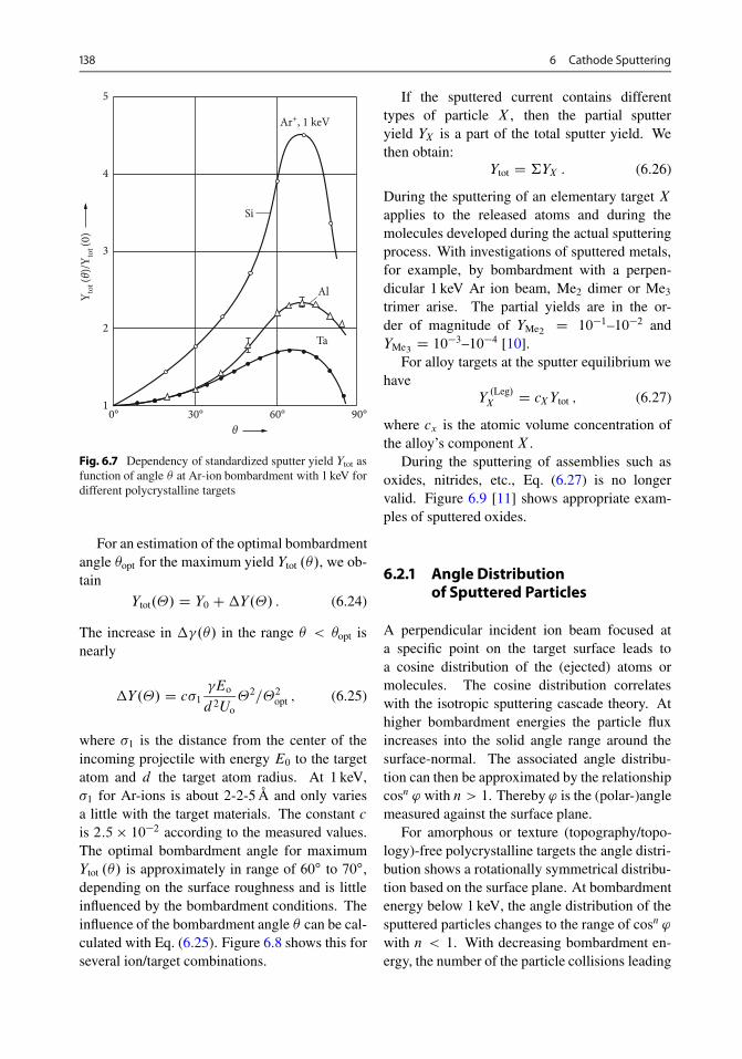
138 6 Cathode Sputtering
5
4
Ar+, 1 keV
Si
Ta
Al
3
2
10° 30° 60°
θ
Y tot (θ)
/Yto
t (0)
90°
Fig. 6.7 Dependency of standardized sputter yield Ytot asfunction of angle at Ar-ion bombardment with 1 keV fordifferent polycrystalline targets
For an estimation of the optimal bombardmentangle opt for the maximum yield Ytot ./, we ob-tain
Ytot.�/ D Y0 C�Y.�/ : (6.24)
The increase in ��./ in the range < opt isnearly
�Y.�/ D c 1 �Eo
d2Uo�2=�2
opt ; (6.25)
where 1 is the distance from the center of theincoming projectile with energy E0 to the targetatom and d the target atom radius. At 1 keV, 1 for Ar-ions is about 2-2-5 Å and only variesa little with the target materials. The constant cis 2:5 � 10�2 according to the measured values.The optimal bombardment angle for maximumYtot ./ is approximately in range of 60ı to 70ı,depending on the surface roughness and is littleinfluenced by the bombardment conditions. Theinfluence of the bombardment angle can be cal-culated with Eq. (6.25). Figure 6.8 shows this forseveral ion/target combinations.
If the sputtered current contains differenttypes of particle X , then the partial sputteryield YX is a part of the total sputter yield. Wethen obtain:
Ytot D †YX : (6.26)
During the sputtering of an elementary target Xapplies to the released atoms and during themolecules developed during the actual sputteringprocess. With investigations of sputtered metals,for example, by bombardment with a perpen-dicular 1 keV Ar ion beam, Me2 dimer or Me3trimer arise. The partial yields are in the or-der of magnitude of YMe2
D 10�1–10�2 andYMe3
D 10�3–10�4 [10].For alloy targets at the sputter equilibrium we
haveY.Leg/X D cXYtot ; (6.27)
where cx is the atomic volume concentration ofthe alloy’s componentX .
During the sputtering of assemblies such asoxides, nitrides, etc., Eq. (6.27) is no longervalid. Figure 6.9 [11] shows appropriate exam-ples of sputtered oxides.
6.2.1 Angle Distributionof Sputtered Particles
A perpendicular incident ion beam focused ata specific point on the target surface leads toa cosine distribution of the (ejected) atoms ormolecules. The cosine distribution correlateswith the isotropic sputtering cascade theory. Athigher bombardment energies the particle fluxincreases into the solid angle range around thesurface-normal. The associated angle distribu-tion can then be approximated by the relationshipcosn ' with n > 1. Thereby ' is the (polar-)anglemeasured against the surface plane.
For amorphous or texture (topography/topo-logy)-free polycrystalline targets the angle distri-bution shows a rotationally symmetrical distribu-tion based on the surface plane. At bombardmentenergy below 1 keV, the angle distribution of thesputtered particles changes to the range of cosn 'with n < 1. With decreasing bombardment en-ergy, the number of the particle collisions leading

6.2 Sputtering 139
Fig. 6.8 Measured valuesagainst the bombardmentangle [9]
1.2
E0= 1.05 keV:
E0= 0.55 keV1.05 keV1.55 keV1.05 keV
Ar+→Cu
Xe+→Cu
Ne+→CuKr+→CuHe+→Cu
NiTiZrPdAgTaAuAl
1.0
0.8
0.6
0.4
0.2
00 0.2 0.4 0.6 0.8
θ/θopt
1.0 1.2 1.4
ΔY(θ
)/ΔY
(θop
t)
to the emission of a surface particle always be-comes smaller.
Thus there is an increase in the probability ofa particle emission in the lateral direction, par-ticularly with target materials that have a highsurface energy barrier. The angle distribution ofthe sputtered particles assumes a torus-like formwith a clear depression in the environment of thesurface plane at bombardment energies around100 eV, Fig. 6.10.
Figure 6.11 shows a comparison betweenmeasured angle distribution with angular ionbombardment and simulation values [13].
6.2.2 Sputtering Effects withSingle-Crystal Solids
The regular structure of the atoms in the bulkmaterial and at the surface of crystalline sputtertargets affects the interaction between the bom-bardment particles and the atoms of the solid lat-
tice and also the properties of the atomic impactcascades which lead to the emission of surfaceparticles. If a single-crystal target is bombardedwith a particle beam of sufficiently small diver-gence parallel to the so-called channel direction(Fig. 6.12), and/or a low indicated lattice direc-tion, then a part of these particles penetrates intothe channel between the tightly packed atomicrows, and the transfer of the bombardment en-ergy takes place at a larger lattice depth. Sincethe energy transfer within the cascade process issmaller at the uppermost atomic layer, the sputteryield Ytot clearly decreases with the bombard-ment along the channel direction.
The channeling property of the crystallinesubstrate depends on the angle of the entrance˚ of the individual ions and on the ion and sub-strate characteristics. If the entrance angle ˚ islarge, then the amplitude of oscillation will belarge, and the ion will not be channeled (trajec-tory a in Fig. 6.12). There will be a maximumpermissible amplitude at which the ion will re-

140 6 Cathode Sputtering
Fig. 6.9 Total and partialsputter yields for the per-pendicular bombardmentof Ta2O3 and Nb2O3 byAr-ions with 600 eV
0.8
ParticleIon
YX
0.6
Ar+→Nb2O5
Nb
NbO
0.4
0.2
0
O
0.8
ParticleIon
YX
0.6
Ar+→Ta2O5
O
TaO
Ta
0.4
0.2
0
1.6
AtomIon
Ytot
1.2
Ar+→Ta2O5
Ar+→Nb2O5
Ar+→TaAr+→Nb [15 – 15]
Ytot→(Ta2O5)Calculated
0.8
0.4
00 700600 eV500400300200100

6.2 Sputtering 141
NiHg+-ions
1000 eV
750 eV
500 eV
250 eV
100 eV
MoHg+-ions 1000 eV
750 eV
500 eV
250 eV
150 eV
Fig. 6.10 Angle distribution of the sputtered particles with perpendicular bombardment of polycrystalline Ni and Mowith Hg ions of different energy [12]
270°1.0 0.8 0.6 0.4 0.2 0
Standardized angle differential yield0.2 0.4 0.6 0.8 1.0
90°
30°
1 keV Ar+, 50°→Ta
60°
330°
MeasurementsSimulationsSmoothRough}
surface
300°
0°
Fig. 6.11 Angle distribution for measured and simulated values for the sputtering of polycrystalline Ta bombardmentwith Ar-ions of 1 keV less than 50ı against the target plane. Different surface roughness are simulated
main channeled (trajectory b in Fig. 6.12); ˚c
is the critical angle that produces this maximumamplitude trajectory.
This critical angle for channeling can be ap-proximated [14] by
˚c D .2Z1Z2e2=4�"0Ed/0:5 : (6.28)
It is clear from this equation that as the ion en-ergy E is increased, ˚c decreases, and has moredifficulty remaining in a stable trajectory. On theother hand, for closely packed atomic rows d de-creases and channeling is easier.

142 6 Cathode Sputtering
Fig. 6.12 Trajectoriesof channeled particles ina crystallographic direction
(E, M, Z)
Ions
Lattice atoms(M2, Z2)
Ψc Ψ
d
Substrate
Channeled iontrajectories
+
+
Dechanneled iontrajectory
(a)
(b)(c)+
4.0AtomIon
3.0
2.0
1.00° 15° 30° 45° 60° 75° 90°
1.5
2.5
3.5
θ
Y tot
Ar+, 1.05 keV→Ge(111)
υ < 100°Cυ > 250°C
[110]
Fig. 6.13 Angle dependence against total sputter yieldof a single-crystal Ge sample by the bombardment of1.05 eV Ar-ions for two different target temperatures. For< 100 ıC the sample surfaces is amorphous by the ionbombardment, > 250 ıC anneals completely during thebombardment
An appropriate example is shown in Fig. 6.13.The figure describes the bombardment of a Gesurface with 111 orientation with 1.05 eV Arions [15]. At a temperature above 250 ıC theatomic structure at the surface of the semiconduc-tor crystal remains uniform, since with thermalannealing he bombardment-induced defect gen-eration prevails at the uppermost atomic layers.
A 110 orientated substrate has a crystal struc-ture with the closest atomic packing and thusthe highest transparency of a single-crystal lat-tice. By ion bombardment, a large penetrationdepth is evident due to the channeling effect. Thechanneling effect leads to a reduction of the sput-ter yield up to an incident beam angle of 35ı.A further increase in the incidence ion angle withrespect to the surface plane as shown in Fig. 6.13at the angle of 70ı – as for D 0ı – leads toa further (111) orientation.
Since the associated lattice channels are farless than in the 110 orientation, the decreasing ofthe sputter yield is less pronounced. Figure 6.13shows the curve of Ytot ./ for the Ge-samplemeasured at temperatures below 100 ıC. Theuniform curve of the bombardment angle depen-dence is to be attributed to the fact that semi-conductors, Ge or Si, become amorphous underbombardment below an annealing temperature.The annealing temperatures for Ge and Si are ap-proximately 250 ıC and 500 ıC.
Semiconductors show a characteristic temper-ature dependence on the sputter yield; an increaseof approximately 10 % Ytot is observed when theannealing temperature is exceeded. A furthereffect, apart from lattice channeling, is the so-called ‘focusing collision’ sequences in tightlypacked lattices [16].
In a certain energy range there is a focus-ing of the transported particle momentum byatomic collisions along a tightly packed atomic

6.4 DC Diode Sputtering 143
10AtomIon
4
00 1 2 3 4 5 keV 6
2
6
8
Ion energy
Y tot
Ar+→ Cu
111
113
122
012123
001
011
Fig. 6.14 The sputter yield against the perpendicularbombardment energy of Ar-ions for differently orientatedsingle-crystal Cu. Arrows on the 111 orientated curveshow the measured values for the electropolished surface
chain. Surface atoms at the end of such atomicchains are preferentially emitted along the appro-priate low indicated lattice directions. Therefore,a strong anisotropy effect of the sputtered par-ticles along the angle distribution is possible,whereby the always existing contribution fromstatistic sputtering cascades are overlaid with fur-ther maxima along the tightly packed lattice di-rections (so-called Wehner spots) [17]. Similarly,the focusing of the surface atoms after emissionfrom the surface can be affected; they may re-combine with the bombardment ion and otheremitted atoms [18]. Figure 6.14 shows the sput-ter yield with perpendicular bombardment withAr-ions for differently orientated single crystalsCu [19]. The characteristics of the sputter yieldof the Cu polycrystalline targets are indicated.
6.3 Coating with Sputtering
The major advantage of sputtering is its general-ity. In principle, any vacuum-compatible mate-rial can be coated by this method [20, 21]. BothDC (direct current) and RF (radio frequency) gas
discharges in a variety of configurations havebeen used. Power is required to generate theplasma from which the useful ions are to be ex-tracted and accelerated to the target. In the casewhere the target material is insulating, meansmust be found to neutralize the surface chargebuilt up on it by the impinging ions. The substrateis bombarded by inert gas molecules, electrons,photons, and negative ions from the plasma, aswell as the desired atoms from the target. Meansto avoid deleterious effects from these extrane-ous sources must be found. Ion bombardmentand discharge pressure lead to internal film stress.Examples of sputtered films and their applica-tions are given in Table 6.1.
In principle, a transition from a high to a lowerlevel of internal stress is possible by increasingthe argon pressure. This is attributed to a de-crease in the ion energies (during the increase inthe pressure).
6.4 DC Diode Sputtering
Figure 6.15 shows the cathodic sputteringmethod with DC-diode assembly. In the chamberthere are two parallel-plate electrodes, one com-posed of the target material and the other of thesubstrate that is to be coated. In the case of DCdischarge, by applying a potential of several kilo-volts (kV) between planar electrodes in an inertgas atmosphere at pressures between 10�1 and10�3 mbar, a glowing plasma is formed, whichis separated from each electrode by a dark space.The plasma is essentially at a constant positivepotential with respect to the cathode.
Electrons are drawn out of the boundary tothe plasma close to the anode and acceleratedacross the anode dark space. The electrons thenstrike the anode, where the energy they carry isdissipated. Ions are drawn out of the other bound-ary of the plasma, accelerated across the cathodedark space (Crooke’s zone), and strike the tar-get cathode, causing sputtering. The plasma isreplenished by electron–ion pairs formed by thecollision of neutral molecules with the secondaryelectrons generated at the cathode surface, accel-erated across the cathode dark space, and injected
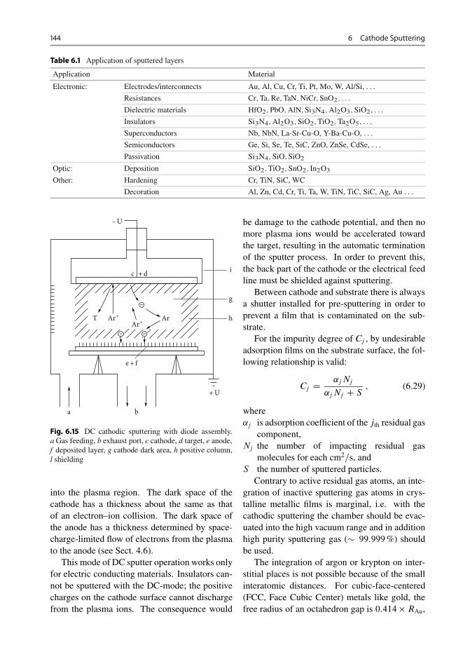
144 6 Cathode Sputtering
Table 6.1 Application of sputtered layers
Application Material
Electronic: Electrodes/interconnects Au, Al, Cu, Cr, Ti, Pt, Mo, W, Al/Si, : : :
Resistances Cr;Ta;Re;TaN;NiCr; SnO2; : : :
Dielectric materials HfO2; PbO;AlN; Si3N4;Al2O3; SiO2; : : :
Insulators Si3N4;Al2O3; SiO2;TiO2;Ta2O5; : : :
Superconductors Nb, NbN, La-Sr-Cu-O, Y-Ba-Cu-O, : : :
Semiconductors Ge, Si, Se, Te, SiC, ZnO, ZnSe, CdSe, : : :
Passivation Si3N4; SiO; SiO2
Optic: Deposition SiO2;TiO2; SnO2; In2O3
Other: Hardening Cr, TiN, SiC, WC
Decoration Al, Zn, Cd, Cr, Ti, Ta, W, TiN, TiC, SiC, Ag, Au : : :
– U
+ U
T Ar+
Ar+ Ar
i
g
h
a b
e + f
c + d
Fig. 6.15 DC cathodic sputtering with diode assembly.a Gas feeding, b exhaust port, c cathode, d target, e anode,f deposited layer, g cathode dark area, h positive column,l shielding
into the plasma region. The dark space of thecathode has a thickness about the same as thatof an electron–ion collision. The dark space ofthe anode has a thickness determined by space-charge-limited flow of electrons from the plasmato the anode (see Sect. 4.6).
This mode of DC sputter operation works onlyfor electric conducting materials. Insulators can-not be sputtered with the DC-mode; the positivecharges on the cathode surface cannot dischargefrom the plasma ions. The consequence would
be damage to the cathode potential, and then nomore plasma ions would be accelerated towardthe target, resulting in the automatic terminationof the sputter process. In order to prevent this,the back part of the cathode or the electrical feedline must be shielded against sputtering.
Between cathode and substrate there is alwaysa shutter installed for pre-sputtering in order toprevent a film that is contaminated on the sub-strate.
For the impurity degree of Cj , by undesirableadsorption films on the substrate surface, the fol-lowing relationship is valid:
Cj D j Nj
jNj C S ; (6.29)
where
j is adsorption coefficient of the jth residual gascomponent,
Nj the number of impacting residual gasmolecules for each cm2=s, and
S the number of sputtered particles.Contrary to active residual gas atoms, an inte-
gration of inactive sputtering gas atoms in crys-talline metallic films is marginal, i.e. with thecathodic sputtering the chamber should be evac-uated into the high vacuum range and in additionhigh purity sputtering gas (� 99:999%) shouldbe used.
The integration of argon or krypton on inter-stitial places is not possible because of the smallinteratomic distances. For cubic-face-centered(FCC, Face Cubic Center) metals like gold, thefree radius of an octahedron gap is 0:414 � RAu,

6.5 Triode Sputtering 145
b
c
b
– 2 kV
Fig. 6.16 Schematic structure of a DC sputtering systemwith incorporation of a magnetic field. a Cathode, b mag-netic coil, c anode
and 0:732 � RNb for cubically body-centered(BCC, Body Cubic Center) metals.
For Nb (R D 0:147nm), the calculated freeradius of a possible foreign atom on a cubicspace-centered surface is:
R D 0:108 nm :
This only permits the entrapment of the small no-ble gas atoms (rHe D 0:093 nm, rNe D 0:112 nm)on interstitial sites. The entrapment of the largerAr- or Kr-atoms would lead to a lattice destruc-tion/deformation. The entrapment of sputter gasatoms in a deposited film is marginal, amountingto a maximum of 10�2 at. % in Ti-films.
Amorphous metallic films can be generatedby quench condensation [22]. Metals such ascopper condense at a temperature of 4 K, ob-taining a nanocrystalline structure (crystallitesize � 3 nm). However amorphous conditionscan be obtained by alloying with other metals.From [23] it is possible to obtain amorphous al-loys, if:� The difference of the atomic diameters �15%.
� The concentration ranges of binary systemsextend to approx. 20 to 80 %.The quantity of the sputter gas entrapped in
the film can be reduced by reducing the gaspressure or in some cases by heating the sub-strate [23]. In order to achieve high sputteringrates with low pressure, the ionization degree of
the sputtering gas must be increased [24]. This ispossible by:� Increasing the probability of ionization of the
existing atoms.� Increasing the number of ionizing electrons.� Using an ion beam source.
By using a magnetic field EB .5 � 10�3 to10�2 T), we can increase the degree of ioniza-tion in the direction of the electron motion. Theelectrons then move helically around the electri-cal stream lines of the field (see Fig. 6.16).
The current density j on the target surfacecan be increased to 5� 10�3 A cm�2 with a sput-ter gas pressure of 10�3 mbar. Coating rates of500 nm=min are then reachable.
6.5 Triode Sputtering
With the triode configuration (Fig. 6.17) theionization level of the plasma is increased byelectrons emitted from a hot cathode and accel-erated in an electrical field. The electrical field isformed by an auxiliary anode.
The cathode is generally a tungsten filamentheated to 2500 ıC or a hollow cathode plasmasource. The anode is a disk or tube with approxi-mately C100V against bias to earth. In addition
e
d TAr+
Ar+
Ar+
Ar+
Ar– –
––
–
––
f
a
b
c
g
h
Fig. 6.17 Schematic structure of a triode arrangement.a Gas feeding, b vacuum port, c glow cathode, d target,e anode, f deposited layer, g auxiliary anode, h magneticcoil

146 6 Cathode Sputtering
Fig. 6.18 Layout ofa sputter system accord-ing to the triode principlewith RF-excitation
Limiting tube
Disc-shapedplasma chamber
Anode
0 ... 300V0 ... 10A
500V0 ... 200mA
1 MHzFilamentsupply
Cathode filament
Sputter target
Substratecarrier
~
to the electrical field, a magnetic field is usu-ally overlaid. The arrangement of the heatingfilament-anode-magnet forms a plasma genera-tion unit that is independent of the substrate andtarget. The potential of the target does not in-fluence the maintenance of the discharge, whichmeans that smaller discharge voltages, 500–000V, are needed. The substrate can also be ar-bitrarily arranged and configured. Figure 6.18shows the concept of triode sputter equipmentwith plasma excitation in combination with anelectron cyclotron wave resonance system [25].
6.6 RF (Radio Frequency) Sputtering
Direct current discharges have difficulties withinitiation of the discharge and with the sputter-ing of insulating materials. These disadvantagesare eliminated by using high frequency arc dis-charges (1–30 MHz). If one of the electrodes iscapacitively coupled to an RF generator, it de-velops a negative DC bias with respect to theother electrode. This is because electrons aremuch more mobile than ions, which hardly re-spond to the applied RF field at all, When the RFdischarge is initiated, the capacitively coupledelectrode becomes negatively charged as elec-trons are deposited on it. However, this chargeis only partially neutralized by positive ions ar-
b
c
a
~~~
Fig. 6.19 Schematic of a high frequency sputtering sys-tem. a Cathode, b high frequency coil, c substrate
cd
b
~~~ HF
Fig. 6.20 Schematic structure of a high frequency sput-tering arrangement in a diode circuit
riving during the negative half-cycle [26]. Sinceno charge can be transferred through the capaci-tor, the electrode surface retrains a negative biassuch that only a few electrons arrive at the sur-face during the next positive half-cycle, and thenet current averaged over the next full cycle iszero. The RF voltage only serves for the genera-tion of the plasma (Fig. 6.19).

6.6 RF (Radio Frequency) Sputtering 147
Current
Current
Plasma
Switch-on phase
Time t
Time t
Time t
Time t
I, V-Curve
Voltage U
Voltage U P
UDC In stationaryoperation
a
b
P
Fig. 6.21 Structure of negative DC voltage at the cathodein high frequency sputter equipment by different veloci-ties of electrons and ions. a Start up state with electronexcess, b shift of the operating point by structure of neg-ative DC voltage at the cathode, so that the total value ofthe current disappears
Ions diffusing from the plasma behave asif only the negative DC bias voltage existedand sputter the negatively charge electrode(Figs. 6.20 and 6.21). The conducting anode,which is directly connected to the power supply,receives pulses of energetic electrons acceleratedessentially to the full amplitude of the RF field.
In the case of gas-discharge sputtering, wherethe substrate is an electrode of the system, the en-ergy dissipated in the sample by electrons fromthe plasma can be substantial. A small amountof heating can be advantageous, since the coat-ing is continuously annealed, which results ina stress-free film. However, excess heating cancause distortion of the film material, and even-tually evaporation of the thin material. Heating
c
aa
b
Fig. 6.22 Schematic of a high frequency sputter systemwith a double cathode. a Cathode, b substrate, c anode
d
ba
c
Fig. 6.23 Schematic of a high frequency sputter systemwith an axial symmetrical double cathode. One electrodeis a circular plate, the other a ring format. a Internal cath-ode, b ring cathode, c substrate, d anode
of the deposited film from electron bombardmentlimits the rate of the film growth that can be uti-lized in sputtering, even before the target heatingeffect. The so-called ‘double cathode’ arrange-ment (Figs. 6.22, 6.23), has the additional benefitof increasing the efficiency of generated ions.
In this system the RF frequency voltage is ap-plied to two cathodes in the recipient, so that theions per half-wave fly to the appropriate cath-ode and thus both electrodes are sputtered. RFsputtering permits the deposition of film from ar-bitrary material, conducting or non-conducting.The system has two, three, or possibly four RFtargets. Figure 6.24 shows the attainable coatingrates. The diagram shows that the deposition rateis directly proportional to the power applied tothe target.

148 6 Cathode Sputtering
Au
Cu
Mn
Si3N4Al2O3
3,02,52,01,51,00,500
2
4
6
8
10
12
14
Rf-power
Coa
ting
rate
μm/h
kW
SiO2
Fig. 6.24 Coating rate as a function of the RF power,target surface area 100 cm2, target/substrate separation25 mm
Fig. 6.25 RF frequencysupply for a sputteringcathode
~~~
Autotuning control mode
M M
Cathode
Matchingbox
Impedancedetector
RF-generator
50 ohmcable
Psoll Pr Pv
Fig. 6.26 Three-chambersputtering system with RF-diode assembly. a Glow,heat, b match element,c target, d plasma, e trans-port device, f substrateplate
b
c d
fe
a
OfOn
With a current density on the target surfaceof 3mA=cm2 and a distance of 25 mm betweentarget and substrate, a coating rate of 6 µm=his possible. With a power density of around1W=cm2 and a distance of 25 mm between sub-strate and target, the substrate temperature canreach up to 400 ıC.
High frequency sputtering is usually operatedwith a frequency of 13.56 MHz. Also systemswith 1 MHz, 2 MHz, 27.12 MHz, 40.68 MHz andwith even higher frequencies are operated.
Industrial RF generators contain a quartz-stabilized oscillator and a power setting enabledby coupled transistor amplifiers up to approxi-mately 5 kW. For high power operation, vacuumtubes (triodes) are used. The RF outputs of suchgenerators are designed with a reflection-freecoaxial conducting cable with a characteristicimpedance .Z/ of 50�, Fig. 6.25.
In the generators output cables are reflec-tometers, which supply signals for the deliveredforward power PV and the reflected power Pr.

6.6 RF (Radio Frequency) Sputtering 149
a
b
c
d
Fig.6.27 RF diode sputtering system with substrate mag-azine. a Target, b heater, c corroding electrode, d substratemagazine
The reflected power shows the deviation of theload impedance from the nominal impedance. Atgood adjustment Pr=PV 2%, the released
Fig. 6.28 Sketch ofa sputtering system withbilateral deposition.a Transmitter connection,b pit, c coupling capacity,d inductance, e currentfeed, f flange, g adjustmentcapacity, h substrate abra-sion, i screen, j substrate,k substrate electrode,l target, m magnet shoe,n pole shoe
a
gh
i
b c d e f
j
k
kmn
l
power is given through the forward powerPV andis regulated over these. Accuracies of approxi-mately ˙5% are reached.
Figure 6.26 shows the schema of a multi-chamber system. In order to degrease the processchamber pumping time and reduce the time re-quired for the pre-treatment of the substrate,a pre-chamber (load lock) is often used for pre-pumping. The substrates arrive over a load lockinto the main vacuum chamber. Afterwards thesubstrates come into the ventilation chamber.The principle of a completely automated sput-ter system is shown in Fig. 6.27. The systempossesses a substrate magazine containing a largenumber of substrates, which are introduced suc-cessively into the sputter chamber. In a prelim-inary stage, the substrates are heat-treated andion-etched. Figure 6.28 shows an RF sputter sys-tem for SiO2 deposition. The target disk consistsof quartz tube coils.

150 6 Cathode Sputtering
6.7 Bias Sputtering
If the substrate is isolated from earth and a neg-ative voltage is applied to the substrate, then thedeposited film is constantly bombarded with ionsfrom the plasma, Fig. 6.29. The deposition filmis continually cleaned by adsorbent gas particlesduring the process.
Bias sputtering can also be combined with anAC source (alternating current) sputtering [27].
6.8 Reactive Sputtering
If an active gas such as oxygen, water, or hy-drogen sulfide is intentionally added to the inertworking gas, it can react with the target materialeither at the target surface or in the gas phase, re-sulting in the deposition of a new compound [28].By varying the pressure of the active gas, controlcan be gained on the stoichiometry of the film.
The products of the dissociation react with thetarget chemically in addition to the bombardmentof the high energy ions. The film deposited at thesubstrate is a combination of the materials fromthe sputtered target and the reactive gas compo-nents. Typical applications are deposited films,whose components possess different vapor pres-sures and hence different sticking coefficients atthe substrate. For example, to generate a SiO2
film with a SiO2 target, Si increases in the de-posited SiOx film (i.e. x < 2). With the additionof oxygen (O2) to the inert working gas (Ar), thecorrect stoichiometry of Si W O D 1 W 2 is ob-tained. Likewise, a pure Si target can be usedto deposit SiO2 films only with the addition of
c b
a
d
Bias0 to 100 V
Fig. 6.29 Schematic of a bias sputtering system. a Cath-ode, b substrate, c insulator, d anode
oxygen gas to the recipient. Silicon dioxide filmshave many applications, e.g. in microelectronicsas insulator films and also as a mask material. Infood technology, PET (Polyethylenterephthalat)bottles are coated in order to improve the diffu-sion barrier.
Another application is the generation ofhigh temperature superconducting films likeYBaCuO, using a YBaCuO target and sputteringwith an O2 additive. The admixture of the fol-lowing additives (often to the working gas Ar) bydissociation creates the appropriate reactive gascomponents:� O2 and H2O ) O-atoms� N2 and NH3 ) N-atoms� CH4 and C2H2 ) C-atoms� SiH4 ) Si-atoms.In principle, ceramics could also be used as tar-gets but they are sensitive to high power fluxes(they break with inhomogeneous heat gradients).Therefore, metal targets are usually used in com-bination with a reactive gas quantity.
In principle there are two operation modes todeposit a multi-component film with a metallictarget (“Compound”):1. Low ion flux and large gas flow ) tar-
get with compound film covered ) coveredmodus.
2. Large ion flux and low gas flow) target re-mains metallic) metallic modus.In the metallic mode larger deposition rates
are obtained than in the covered mode. If we keepthe ion flux constant and vary the gas flow, we re-ceive a transition of one to another mode. Thistransition shows a hysteresis (Fig. 6.30), whichstarts in the metallic mode and increases the gasflow, then the plasma “jumps” with a certain gasflow �m!b into the covered mode, whereby thedeposition rate clearly becomes smaller. If wenow again reduce the gas flow, the transition tothe metallic mode takes place at a smaller gasflow �b!m:
�m!b > �b!m :
In stationary condition the deposition rate ofcompound material at the target is equal to theerosion rate by sputtering of the compound mate-

6.8 Reactive Sputtering 151
0.61.00.80.60.40.20.2
0.3
0.4
0.5
0.60.7
0.8
0.9
1.0
1.1
0.0Mass flow [sccm]
Ti-L
ine
Fig. 6.30 A Ti-line compensated hysteresis with the re-active sputtering deposition of TiN layers (measured val-ues)
rials from the target:
n0T
d�T
dtŠD 0 D i�reasrea.1 ��T/� �ion�C�T :
(6.30)
For the description a simple model is used, withfollowing denotations:� AT and AS are the surfaces of the target and
the substrate.� �T and �S are the surface degrees of cover-
age from target and substrate with compoundmaterial.
�M and �C are the sputtering rates (target) of themetal and the compound materials at the tar-get.
�ion is the ion flux.�rea is the flow of the reactive gas molecule.srea is the sticking coefficient of these gas
molecules on the metallic target.Here i is the number of radicals created in theplasma by dissociation (e.g. O-radical from O2:i D 2, C-radical from CH4: i D 4). Thefirst term describes the flow of the reactive gasmolecules (�rea), which are dissociated in theplasma (i) adhering to the target naturally onlyon a still free surface (1 ��T).
The second term in Eq. (6.30) designates thesputtering of the compound film through bom-barding ions (�ion) with the yield �C, where this
can naturally only take place with an already cov-ered surface of the target (�T).
We now consider the coverage of the substrate�S in the stationary condition; those reactivegas molecules striking the metallic part of thesubstrate (1��S) are increased. Further this is in-creased by the flux of compound material, whichis sputtered from the target and strikes on the free,i.e., metallic, surfaces of the substrate (1 ��S).
The coverage of the substrate is decreased bypart of �S of the flux of sputtered metal atomsYM�ion, which come from the target (1 � �T),which strikes on the substrate surface coveredwith compound material (�S). If we now stillconsider the relationship from target to substratesurface (AT=AS), then we obtain:
n0S
d�S
dtŠD 0
D i�reasr.1 ��S/C �ion�C�TAT
AS.1 ��S/
� �ion�M.1 ��T/AT
AS�S : (6.31)
If we describe the total number of reactive gasmolecules that are used per second in order togenerate a compound film on the substrate, thenwe obtain:
dNrea
dtD �reasrŒ.1��T/AT C .1 ��S/AS� ;
(6.32)since the reactive gas flux goes equally to the sub-strate and to the target. The flux by which thetarget is sputtered, that is that the target flows offafter the sputtering of the metallic part and thecompound fraction, is:
�sput D �ionŒ�M.1 ��T/C �C�T� : (6.33)
Now Eq. (6.30) can be resolved after covering ofthe surface of the target:
�T D i�reasr
�ion�C C i�reasr: (6.34)
Likewise (6.31) can be resolved after the cover-ing of the surface of the substrate, and T insertedafter (6.34):

152 6 Cathode Sputtering
�S D1C AT
AS
�i�C�i�CCi�rSr
1C �iATAS
h�C
1�i�CCi�rSr
C �M
�1
i�rsr� 1
�i�CCi�rSr
�i : (6.35)
If we insert Eqs. (6.34) and (6.35) into (6.32)and in (6.33), we have the hysteresis problem thatwas addressed before.
With reactive sputtering many interfaces canbe produced. Thus, a multiplicity of hard mate-rial combinations are created on the basis of car-bides, nitrides and oxides and/or their sputteredmixtures of metals. They are frequently abrasivewear-preventing and anticorrosive [25, 29, 30].
6.9 Magnetron Discharges
The high flexibility of sputtering techniques isalso based on various magnetically confined dis-charge configurations. By means of the E � B ,drift plasmas of high density within a closely lim-ited range can be concentrated [31, 32].
6.9.1 Structure
A typical magnetron configuration is shown inFig. 6.31. It consists of electrodes that are con-nected with a DC voltage VDC (above the cathode,under the anode). Above the cathode a systemof permanent magnets is arranged so that thecylinder-symmetrical chamber makes a circularpenetration of the magnetic field possible. The
AnodeIDC
+
–
CathodeSoft iron cross
MagnetS N S N
rCE W R
VDC DC-glow discharge
S
D
Fig. 6.31 Planar magnetron. Electrons originating at thecathode surface are confined by the fields of permanentmagnets placed behind the cathode
center radius of the ring is R, the width of thering w and the height rce. If we apply a voltageVDC and ignite a glow discharge, we obtain a highdensity, brightly shining plasma within the rangeof the magnetic field. Outside of the circular fieldthe plasma density is lower.
In the environment of the cathode a skin layerforms with the thickness s � 1mm.
6.9.2 Function of theMagnetron
Positive inert gas ions attain kinetic energy inthe cathodic skin layer and bombard the (cold)cathode, which is configured as a target. On bom-bardment the target material sputters and diffusesinto the discharge. The mean free paths of thesesputtered particles are in the range of the dis-tance between anode and cathode. If a substrateis on the anode, this is coated with the targetmaterial. Additionally, the ion bombardment ofthe cathode causes the emission of secondaryelectrons from the target. These are repelled bythe cathode and penetrate into the bulk plasma,where they are held by the magnetic field lines.The electrons collide with the available neutralparticles and ionize these.
A typical magnetron discharge parameter is asfollows:B0 � 200G D 0:02T (magnetic flow density
with the radius R).p � 0:3–0:7� 10�2 mbar .jion � 20mA=cm2 (over the torus averaged ion
current density).VDC � 800V .The loss of energy of the electrons pro electronion pair is EC.
Electrons in the discharge lose energythrough:� Ionization� Excitation� Elastic collisions (elastic scattering).
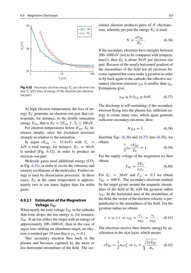
6.9 Magnetron Discharges 153
103
103
103
1 10Te[eV]
E c[eV
]
100
ArO2
Fig. 6.32 Necessary electron energy EC per electron–ionpair Te [eV] (loss of energy of the electrons per electron–ion pair)
At high electron temperatures the loss of en-ergy EC generates an electron–ion pair that cor-responds, for instance, to the double ionizationenergy Eion, that is EC � 2Eion f . Te � 100 eV.
For electron temperatures below Eion, EC in-creases steeply, since the excitation increasesstrongly in relation to the ionization.
In argon (Eion D 15:8 eV) with Te �4 eV a total energy, for instance, EC � 40 eVis needed (Fig. 6.32), in order to produce anelectron–ion pair.
Molecule gases need additional energy (CO2
in Fig. 6.31), in order to excite the vibratory androtatory oscillations of the molecules. Further en-ergy is used by dissociation processes. In thesecases, EC at the same temperature is approxi-mately two to ten times higher than for noblegases.
6.9.2.1 Estimation of theMagnetronVoltage VDC
When nearly the total voltage VDC in the cathodicskin zone drops, the ion energy is, for instance,VDC. If an ion strikes the target with an energy ofapproximately 200–1000 eV, then in the case ofargon ions striking an aluminum target, an elec-tron is emitted per 10 ions that is �se � 0:1.
This secondary electron flies back to theplasma and becomes captured by the more orless horizontal streamlines of the field. The sec-
ondary electron produces pairs of N electrons–ions, whereby per pair the energy EC is used:
N � eVDC
EC: (6.36)
If the secondary electrons have energies between200–1000 eV (not to be compared with tempera-tures!), then EC is about 30 eV per electron–ionpair. Because of the nearly horizontal gradient ofthe streamlines of the field not all electrons be-come captured but some make a gyration in orderto fly back again to the cathode, the effective sec-ondary electron emission �eff is smaller than �se.Estimations give:
�eff Š 0:5�se Š 0:05 : (6.37)
The discharge is self-sustaining; if the secondaryelectron flying into the plasma has sufficient en-ergy to create many ions, which again generatesufficient secondary electrons, then:
N�eff D 1 : (6.38)
Inserting Eqs. (6.36) and (6.37) into (6.38), weobtain:
1
2�seeVDC
ECD 1 : (6.39)
For the supply voltage of the magnetron we thenobtain:
VDC � 2EC
e�se: (6.40)
For EC D 30 eV and �se D 0:1 we obtainVDC D 600V. The secondary electrons emittedby the target gyrate around the magnetic stream-lines of the field of B0 with the gyration radiusrCE. In the horizontal area of the streamlines ofthe field, the vector of the electron velocity is per-pendicular to the streamlines of the field. For thegyration radius we obtain:
v D ! � r ) rCE D v?!CED ve
!CE: (6.41)
The electrons receive their kinetic energy by ac-celeration in the skin layer, which means:
eVDC D 1
2mev
2e ) ve D
s2eVDC
me: (6.42)

154 6 Cathode Sputtering
Fig. 6.33 Schematic illus-tration of the magnetronprinciple at the cathodesurface
Cathode
r1
r2
rCE
RCθ
W/2B
R
To determine the angular frequency, we usedthe equilibrium of forces between the centrifugalforce and the Lorentz force:
qv � EB D m2
r) qB � e!rB D m!2r
) ! D eB
m: (6.43)
Inserting Eqs. (6.42) and (6.43) into (6.41), weobtain:
rCE D 1
B0
r2meVDC
e; (6.44)
for B0 D 200G and VDC D 600V rCE � 5mm.Under the same conditions for argon ions weobtain gyration radius of rAr � 1:3m. Foran approximation of the ring width w, we musttake 6.33 into account.
Figure 6.33 shows a part of the cathode fromFig. 6.31. The mean part of the plasma ring un-der the cathode corresponds, for instance, to thegyration radius rCE of the electrons around thehorizontal streamlines of the magnet field (morein the center, less at the edge).
For further calculations, it is accepted that thethickness of the skin layer is much smaller thanthe gyration radius, i.e. s � rCE. If secondaryelectrons are emitted, these keep up with thestreamlines of the magnet field and travel alongthem (v ¤ 0). Thus, they arrive at the edge of theskin layer with r1 and r2, where they are reflectedback due to the large barrier potential. Thus, theymove between the two radii. If we accept the ra-dius of curvature of the B-lx ines of flux to beRC,and the height of the ring as rCE and the width asw � r2 � r1, then we obtain:
sin D w=2
RC) RC sin D w=2 : (6.45)
Furthermore:
rCE CRC cos D RC ) RC cos D RC � rCE :
(6.46)After squaring Eqs. (6.45) and (6.46) and addingthe two equations together, we obtain:
R2C.sin2 C cos2 / D .RC � rCE/2 C w2
4:
(6.47)With sin2 C cos2 D 1 we obtain for w:
w2 D 4 �2RCrCE � r2CE
�: (6.48)
Then inserting into Eq. (6.47) the value alreadycalculated for rCE D 0:5 cm and a typical valueof RC D 4 cm, the ring width is:
w � 3:8 cm :
The pressure for magnetron discharges is verysmall, thus there are no collisions in the outerzone. At the edge, the layer thickness, s, is smalland there is a relatively high voltage (VDC) drop.Therefore, the ion current density of the ring atthe cathode can be calculated with “the U3=2”from the Child-Langmuir law:
Nji D 4
9"0
s2e
mion
V3=2
DC
s2; (6.49)
with the dielectric constant "0 and the ion massmion. At the same time, the ion current densitycorresponds to the entire discharge current di-vided by the ring surface:
Nji D IDC
�.r22 � r21 /D IDC
�.r2 � r1/.r2 C r1/ :(6.50)

6.9 Magnetron Discharges 155
ne= ni= n0
ne= ni
ϕp
ϕ(0) = 0ϕ(0) ≈ 0
nb= bulkns : Film skin
n(x)
x = 0
x
Film
Film skin
Pre-filmPlasma
Fig. 6.34 Course of the plasma density on the magnetronsurface
For r2 � r1 D w and for r2 C r1 � RC w=2 weobtain:
NjiIDC
�.Rw Cw2=2/ : (6.51)
Using the calculated value ofR D 4 cm andw D3:8 cm and a typical discharge voltage of IDC D5A, we obtain:
Nji D 5A
70:4 cm2� 71mA
cm2:
Applying this value in Eq. (6.48), we obtain forthe thickness of the edge layer:
s � 0:6mm :
The above assumption that s � rCE .D 5mm/ isjustified.
6.9.3 Estimation of Plasma Density
To determine the plasma density in the mag-netron, we consider the plasma skin layer [33].
The plasma is divided into bulk, pre-layer andlayer edge. The plasma density at “the interface”,between bulk and pre-layer is designated by bulkdensity nb. The density at the layer edge, i.e. “theinterface” between pre-layer and layer, is desig-nated by ns. The potential with nb is Fp, whichwith ns is set to zero, i.e. Fs D 0. The ions are
accelerated in the pre-film with the Bohm veloc-ity vB, i.e.
B DskTe
mion(6.52)
is the velocity of the ions at the film edge(Fig. 6.34). When the ions move through the pre-film potential, the ion acquires the energy:
1
2mion
2B D e˚p : (6.53)
With Eq. (6.43), we obtain:
kTe D 2e˚p : (6.54)
In order to determine the plasma density of theedge layer ns, the Boltzmann equation in regardto the bulk density: nb is required:
ns D nb exp.�e˚p=kTe/ : (6.55)
So extrapolating from (6.54), we obtain:
ni;s D nsnb exp.0:5/ � 0:61nb : (6.56)
Now the ion current density can be expressed:
Nji D eni;ss D 0:61 � enbB ; (6.57)
and/or with (weak) Te dependence the ion densitycan be determined:
ni DNji
0:61e
rmi
kTe: (6.58)
For Te � 3 eV and a calculated current density ofji � 70 � 10�3 A=cm2 D 700A=m2, we obtainfor the ion density:
ni D ne D 700
0:61 � 1:6 � 10�19
�r
40 � 1:67 � 10�271:38 � 10�23 � 3 � 11604
D 2:67 � 1018 1m3
D 2:67 � 1012 1
cm3:
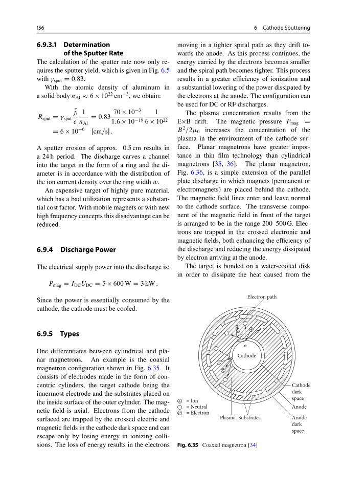
156 6 Cathode Sputtering
6.9.3.1 Determinationof the Sputter Rate
The calculation of the sputter rate now only re-quires the sputter yield, which is given in Fig. 6.5with �sput D 0:83.
With the atomic density of aluminum ina solid body nAl � 6 � 1022 cm�3, we obtain:
Rsput D �sput
Nji
e
1
nAlD 0:83 70 � 10
�3
1:6 � 10�191
6 � 1022D 6 � 10�6 Œcm=s� :
A sputter erosion of approx. 0.5 cm results ina 24 h period. The discharge carves a channelinto the target in the form of a ring and the di-ameter is in accordance with the distribution ofthe ion current density over the ring width w.
An expensive target of highly pure material,which has a bad utilization represents a substan-tial cost factor. With mobile magnets or with newhigh frequency concepts this disadvantage can bereduced.
6.9.4 Discharge Power
The electrical supply power into the discharge is:
Pmag D IDCUDC D 5 � 600W D 3 kW :
Since the power is essentially consumed by thecathode, the cathode must be cooled.
6.9.5 Types
One differentiates between cylindrical and pla-nar magnetrons. An example is the coaxialmagnetron configuration shown in Fig. 6.35. Itconsists of electrodes made in the form of con-centric cylinders, the target cathode being theinnermost electrode and the substrates placed onthe inside surface of the outer cylinder. The mag-netic field is axial. Electrons from the cathodesurfaced are trapped by the crossed electric andmagnetic fields in the cathode dark space and canescape only by losing energy in ionizing colli-sions. The loss of energy results in the electrons
moving in a tighter spiral path as they drift to-wards the anode. As this process continues, theenergy carried by the electrons becomes smallerand the spiral path becomes tighter. This processresults in a greater efficiency of ionization anda substantial lowering of the power dissipated bythe electrons at the anode. The configuration canbe used for DC or RF discharges.
The plasma concentration results from theE�B drift. The magnetic pressure Pmag DB2=2�0 increases the concentration of theplasma in the environment of the cathode sur-face. Planar magnetrons have greater impor-tance in thin film technology than cylindricalmagnetrons [35, 36]. The planar magnetron,Fig. 6.36, is a simple extension of the parallelplate discharge in which magnets (permanent orelectromagnets) are placed behind the cathode.The magnetic field lines enter and leave normalto the cathode surface. The transverse compo-nent of the magnetic field in front of the targetis arranged to be in the range 200–500 G. Elec-trons are trapped in the crossed electronic andmagnetic fields, both enhancing the efficiency ofthe discharge and reducing the energy dissipatedby electron arriving at the anode.
The target is bonded on a water-cooled diskin order to dissipate the heat caused from the
= Ion= Neutral= Electron
Plasma Substrates
Anode
Anodedarkspace
Cathodedarkspace
Cathode
e
Electron path
Fig. 6.35 Coaxial magnetron [34]

6.9 Magnetron Discharges 157
Grounded high-grade steel screen
Titan targetMagnet arrangement
Isolation materialPower supply
Water coolingChamber wall
Copper
Fig. 6.36 Intersection through a planar magnetron
Substrate
Plasma
Sputtered neutrals
Ions
Permanentmagnet
Disc-shaped anode
NSN
S
Ring-shapedcathode
= Ions= Neutral
Fig. 6.37 Circular magnetron. Electrons originating atthe cathode are confined by fields from permanent mag-nets placed behind the cathode. They lose energy in spiralpaths in the plasma and are collected by the disk anode.The substrate, not being an electrode of the system, col-lects only sputtered neutrals
ion bombardment [37, 38]. Circular magnetrons(sputter guns or “S” guns) in which the cathodeis in the form of a ring that surrounds a planardisk-shaped anode are also popular (Fig. 6.37).
Magnets behind the cathode enhance the dis-charge and the electrons are collected by theanode. A large fraction of the sputtered materialfrom the target cathode is ejected in a forwarddirection and deposited on a substrate that nolonger needs to be an electrode of the system.This way, very high power densities (50W=cm2)in the erosion zone of the target can be dissi-pated. The main disadvantage of planar andcircular magnetrons is the fact that the depositionrate is not uniform across the region where thesubstrates are placed. This, as in evaporation, is
overcome by an appropriate mechanical motionof the substrate table so that each substrate is ex-posed to the same average flux.
6.9.6 Cathodes
Table 6.2 shows some examples of sputter tech-nology application, including the film functionsand the materials used, and in Table 6.3 therespective requirements of the arranged targetsare shown [37]. Targets are manufactured invacuum by induction or electron-beam meltingwith subsequent casting into the desired form.Targets of high melting materials or from highmelting compounds that are technically not pro-ducible can be manufactured metallurgically bypressing of powders followed by sintering or hot-pressing. Rectangular targets are used especiallyfor manufacturing films on large surfaces, suchas paper, plastic foils, windowpanes or otherlarge-scale substrates. For DC voltage sputteringmagnetrons, cathodes up to 350 cm in length areused for the production of thin films. Figure 6.38shows some forms of cathodes.
Fig. 6.38 Different target forms before and after use

158 6 Cathode Sputtering
Table 6.2 Examples of application of cathodic sputtering
Sector Thin film function Material
Microelectronic Circuit path and contactsBuffer layers
Al, Al-alloysTi, W, WTi, Cr silicide(TaSi2;MoSi2)Noble metals
Data storage Magnetic storage layer for rigid disksOptic and magneto-optic memory
Co-alloys(CoNiCr)Cr, CFeCo-rare-earth-alloysAl, Si
Deposition of glass Thermal insulation layerColoration of glassHeated windows
Sn, InSn, ITO(In2O3=SnO2)Ag, NiCr
Display technology Electrodes for liquid crystal readouts ITO (In2O3=SnO2)
Hard material layers Wear reducing layers for tools TiN, TiAIN, HfN
Decorative coatings Wear resistant decorative coatings(gold imitation, anticorrosive)
TiN, Au-alloys
Table 6.3 Requirements at targets
Application Requirements/problems
Microelectronic(Al, Cr, WTi, Silizide)
Purity .> 5N/Avoidance of alkali impuritiesAvoidance of alpha emitters(U, Th)Avoidance of precipitationsuniform structure low O2 con-tent
Magnetic layers(Co-Basis, Ni-Basis)
Low magnetic permeabilityAvoidance of precipitationsPurityStructure
Coating of glass(Sn, InSn, ITO)
Homogeneity (up 3 m)Avoidance of particle forma-tionCost
Hard materials layersCorrosion protectionlayers
Avoidance of particle forma-tionCost
The largest erosion ditch at the magnetrontarget surface is formed in the range where theelectrical field and the magnetic field are perpen-dicular to each other. To increase the utilizationrate, different possibilities are available. Themethod most frequently applied with round cath-odes moves the magnets in form of Lissajousfigures. Thus the utilization rate increases, theerosion of the target is more evenly distributed
and hence there is an improved homogeneity ofthe film thickness.
Under continuous production conditions hightarget utilization rates with constant sputteringconditions are necessary. This is only possibleby stabilization of the discharge parameters, withrespect to the erosion profile, Fig. 6.39.
Figure 6.40 shows the dependence of the mag-netic field force for different target thicknessesand the associated reduction in the dischargevoltage for two different intensities of current.The operating point of the discharge is not onlyregulated by the power of the current supply.A reproducible coating process is only possiblewith stabilization of the magnetic field force atthe target surface [38].
A constant magnetic field force can be at-tained by adjusting the height of the mag-netic system according to the target erosion,Fig. 6.41 [38].
The lifting system also has the advantage thatthere is around a 5 to 10 % increase of the tar-get utilization. The target utilization can be alsoimproved substantially with an interpol target,Fig. 6.42 [39]. The magnetic field lines devi-ate parallel to the target surface; target erosion ismore homogenous. So that the electrons do notescape out of the plasma, the pole pieces havea floating potential. Interpol targets are availablein a round or rectangular form. A round cathode

6.9 Magnetron Discharges 159
Fig. 6.39 Sectional cross-section through an erodedtarget during a typicalutilization of 25–30 %
–10–20–30–40 30 mm2010 40
2
3
4
5mm
Measured profile
Extrapolated profile by erosion of the target
t
1
0
6
46Target thickness d
814 mm 02 500Discharge voltage U
400300
700
600
500
400
300
200
100
800Oe
800600 V
I= 10 AI= 5 A
Mag
netic
fiel
d H
x
Fig. 6.40 Correlation between the effective magneticfield Hx , the effective target thickness d and the result-ing discharge voltage U (parameter: discharge current I )
can be used with a power density of 205W=cm2
in continuous operation. At a substrate distanceof 50 mm, it is possible to obtain a coating rate of201 nm=s. The density of the sputtered particlesis so high that a sufficient number of the parti-cles are ionized, and hence the sputter processcan be maintained without noble gas discharge.With copper, the density of the ions is alreadyhigh enough so that with a discharge power of80W=cm2 no argon is necessary [39].
Reactive sputtering with magnetrons in thedirect current modus has the disadvantage thatarcing is a frequent occurrence. The reason isshown in Fig. 6.42.
Radial movement
Verticalmovement c
ea
b
d
Fig. 6.41 Representation of the lifting mechanism in thesectional view. a Cooling, b retaining plate, c raising sys-tem, d magnetic cross-head, e target
Within the internal ranges of the erosion ditch,the ion current density becomes so high that nooxide or other insulator material is generated. Onthe sides of the discharge ditch a strong drop-offof the ion current density occurs. This finally re-sults in fast creation of oxides and nitride films.These films lead to arc discharges. With the highdischarge current at the points of breakthroughmaterial evaporates, and subsequently particlesstrike the substrate, which leads to irregularitiesin the film. A reduction of the discharge arcs canbe reached with an improvement of the interpolmagnetron, Fig. 6.43.
A shutter between target and substrate and thegas inlet in the vicinity of the substrate cause a re-duction of reactive gas transport to the target andalso a reduction of the condensation rate. An AC
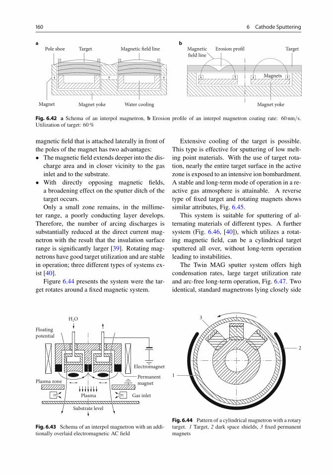
160 6 Cathode Sputtering
Pole shoe Target Target
Magnet yoke Magnet yoke
Magnets
Water cooling
Erosion profilMagneticfield line
a bMagnetic field line
Magnet
Fig. 6.42 a Schema of an interpol magnetron, b Erosion profile of an interpol magnetron coating rate: 60 nm=s.Utilization of target: 60 %
magnetic field that is attached laterally in front ofthe poles of the magnet has two advantages:� The magnetic field extends deeper into the dis-
charge area and in closer vicinity to the gasinlet and to the substrate.
� With directly opposing magnetic fields,a broadening effect on the sputter ditch of thetarget occurs.Only a small zone remains, in the millime-
ter range, a poorly conducting layer develops.Therefore, the number of arcing discharges issubstantially reduced at the direct current mag-netron with the result that the insulation surfacerange is significantly larger [39]. Rotating mag-netrons have good target utilization and are stablein operation; three different types of systems ex-ist [40].
Figure 6.44 presents the system were the tar-get rotates around a fixed magnetic system.
Electromagnet
Permanentmagnet
Gas inletPlasma
Plasma zone
Floatingpotential
H2O
Substrate level
Fig. 6.43 Schema of an interpol magnetron with an addi-tionally overlaid electromagnetic AC field
Extensive cooling of the target is possible.This type is effective for sputtering of low melt-ing point materials. With the use of target rota-tion, nearly the entire target surface in the activezone is exposed to an intensive ion bombardment.A stable and long-term mode of operation in a re-active gas atmosphere is attainable. A reversetype of fixed target and rotating magnets showssimilar attributes, Fig. 6.45.
This system is suitable for sputtering of al-ternating materials of different types. A furthersystem (Fig. 6.46, [40]), which utilizes a rotat-ing magnetic field, can be a cylindrical targetsputtered all over, without long-term operationleading to instabilities.
The Twin MAG sputter system offers highcondensation rates, large target utilization rateand arc-free long-term operation, Fig. 6.47. Twoidentical, standard magnetrons lying closely side
3
2
1
Fig.6.44 Pattern of a cylindrical magnetron with a rotarytarget. 1 Target, 2 dark space shields, 3 fixed permanentmagnets

6.9 Magnetron Discharges 161
3
2
1
Fig. 6.45 Schema of a cylindrical magnetron with rotarymagnets. 1 Target materials, 2 dark space shields, 3 rotarypermanent magnets
2
3
1
Fig. 6.46 Schema of a cylindrical magnetron with sput-tering of the entire lateral surface. 1 Target, 2 rotarypermanent magnets, 3 anode
by side form a unit. On both cathodes an ACvoltage is applied with a frequency of some kHz.At one-half periods, one magnetron serves as thecathode, the other as the the following half-wavethe polarity is inverted. The consequence is thatany generation of an insulating layer on the targetedge will be uncharged in the second half-periodas it switches anode polarity. Therefore, no highvoltage develops, which could lead to a break-through.
6.9.7 Shutters
At start-up or after a long operation time, the re-cipient must ventilate or the working gas must
Elect. interface
Plasma
Substrate
Fig. 6.47 Schema of a twin-MAG sputtering system
1
2
3
40°
Fig. 6.48 Distribution shutter for a magnetron cathodeof 200 mm in diameter. 1 Cathode, 2 distribution shutter,3 circular ring provable with substrates
be changed. Thereby, impurities or out-gassingproducts from the target must be eliminated. Inlarge manufacturing facilities, a pre-sputteringconditioning process with no test substrate ortest substrates is used, or in the case of smallersystems, a shuttering screen is used. Substratecleaning by particle bombardment or structuringof target layers by etching must likewise involvea shutter to protect the target surface against im-purities. When substrate coating with a roundcathode is used, a shutter for homogeneous dis-tribution of the film thickness is necessary. Fig-ure 6.48 shows an example of a distributionshutter.

162 6 Cathode Sputtering
b
a
Discharge duration
0 2 4 6 8 10min
100
200
300
400
°C
Subs
trat
e tem
pera
ture
Fig. 6.49 Substrate heating up with a DC voltage dis-charge; a D 0:74W=cm2 ; b D 1W=cm2
6.9.8 Infrared Heating
For homogeneous film deposition, not only con-stant discharge parameters should be taken intoconsideration but a constant substrate temper-ature is also necessary. The coating processusually begins with a lower substrate tempera-ture and subsequently increases due to particlebombardment. Until temperature equilibrium isreached, a difference in film morphology and,therefore, in film properties will be occur. Fig-ure 6.49 illustrates this, whereby all three ther-mal factors, heat conductivity and heat transitioncoefficients, influence the curve progression. In-frared heating before starting the coating processimproves the homogeneous structure of the film.
6.9.9 Rate and Film ThicknessMeasuring Instruments
Whereas with vacuum evaporation the evapora-tion rate increases exponentially with the sourcetemperature, the coating rate during cathodicsputtering and the condensation rate are far lesscritically dependent on the discharge parameters.
One can usually tune in rate or film thicknessmeasuring instruments generated with discharge
Ta2O5
SiO2
1 3 5 7 9 11 13 15
2 4 6 8 10 12 140.8
0.9
1.0
1.1
0.9
1.0
1.1
1.2
1.3
Coa
ting
time (
stan
dard
ized
)
Fig. 6.50 Standardized representation of the coating du-ration of the individual �=4-layer at the production of fourequal edge filters
CathodeTest glass
Anode
High voltagesupply
Beam splitter
Photodiode formeasured light Chopper
Lamp
Sight glassMonochromator
Photodiode forreference light
Chart recorder
Phase-sensitiveamplifier
„0“ddt
Fig. 6.51 Pattern of optical measuring instrument for ca-thodic sputtering plants
parameters, selecting for each case a desired filmthickness over the time period of the sputteringprocess.
For determination of the coating rate as a func-tion of the process parameters the use of a quartzcrystal oscillator is useful. Without interruptionof the vacuum (in situ) all relevant parameterscan be determined. There are exceptions whenexact control of the film thickness and opticallyeffective films with high precision demands arenecessary during the coating procedure. Sput-tering of a SiO2-target is very sensitive to theresidual gas. According to Fig. 6.50 [41], the

6.9 Magnetron Discharges 163
a
b
c
d
Fig. 6.52 Process steps in a cathodic sputtering plantwith air-lock; a Introducing the substrates to be coated inthe load lock, b Pretreatment of the substrates, c Introduc-ing the substrates into the coating chamber, d Dischargeof the substrates from the load lock, the substrates coating
deposition duration necessary for generating thefirst SiO2 film is substantially longer than for thefollowing films where the inside of the equipmentis better conditioned.
Figure 6.51 [42, 43] shows the schema of anoptical measuring instrument that uses the mini-mum/maximum method to obtain an exact signalfor a given film thickness. The condensation ratefor depositing a SiO2 film is so constant that it isnot necessary to use a PID (proportional-integral-
2 2 2 2
554
2 2
33883
3
1199
2
7 7
1g1f1e1d1c1b1a
7
Fig. 6.53 Schema of a sputtering plant with seven modules. 1a Loading module, 1b lock-in module, 1c processmodule, 1d process module, 1e process module, 1f lock-out module, 1g reloading module, 2 transport system, 3 valve,4 lifting device for HF-etching or for cooling, 5 turbo-molecular pump or cryopump, 6 electrical matching elements,7 pre-vacuum pump, 8 substrate heating, 9 DC or RF cathode, 10 DC or RF magnetrons, 11 cooling station
derivative) controller. The optical instrumenta-tion serves as a thickness monitor only.
6.9.10 Two-Chamber Equipment
The film properties are only reproducible if theresidual gas does not have a noticeable influ-ence during the deposition. This requires a higheffective pump speed and sufficient recipient con-ditioning. Moisture, recipient temperature andcleanliness after each ventilation or conditioningprocedures will result in different partial pres-sures of the residual gases. With a load lock ar-rangement in which the coating chamber remainsunder constant vacuum, these disadvantages donot arise. The simplest form of load lock arrange-ment is shown in Fig. 6.52
The chamber and the load lock are separatedby a valve. During the recovery of the coatedsubstrate and the evacuation of the load lock thisvalve remains closed. The residual gas condi-tions in the coating chamber can be kept constant,which saves long conditioning times. These sim-ple load lock installations do not offer optimaluse of the substrate transport and the pump downtime. With a double transport system this dis-advantage is eliminated. Two substrate carrierscan be treated at the same time, since the loadlock chamber possesses two transportation levels.While the processes are executed in the coating

164 6 Cathode Sputtering
chamber, the second substrate carrier is loadedinto the load lock (Fig. 6.53a) and then evacua-tion and pre-treatment steps are possible (heating,etching) (Fig. 6.53b). After coating, there is anexchange of processed and non-processed sub-strates. Subsequently, the coated substrate isremoved and the sputtering process is only inter-rupted briefly.
6.9.11 Multi-Chamber Equipments
Multi-chamber systems are arranged in a mod-ular construction, which offers large productioncapacity and flexibility, in addition to optimumreproducibility for production of different filmsystems. All pre and post-treatments, includ-ing different sputtering options with any numberof integrated cathode arrangements, are possible.Figure 6.53 shows a seven-module design.
References
1. Westwood WD (2003) Sputter Deposition AVS Edu-cation Committee Book Series, vol. 2
2. Ziegler JF, Biersack JP, Littmark U (1984) The Stop-ping and Range of Ions in Solids Stopping and Rangesof Ions in Matter, vol. 1. Pergamon Press, New York
3. Ortner K, Birkholz M and Jung T (2003) “NeueEntwicklungen beim Hohlkatoden-Gasflusssputtern”.Vac. Praxis (in German) 15: 236–239 M. Birkholzand T. Jung (2003). Vac. Praxis (in German) 15: 236–239
4. Sigmund P (1987) Mechanisms and theory of physicalsputtering by particle impact. Nucl Instr Meth PhysRes B 27:1
5. Binder K (1992) The Monte Carlo Method inCondensed Matter Physics. Springer, Berlin[u. a.], ISBN 3-540-54369-4; 2. Auflage, 1995,ISBN 3-540-60174-0
6. Binder K, Landau DP (2000) A Guide to Monte CarloSimulations in Statistical Physics. Cambridge Univer-sity Press, Cambridge [u.a.], ISBN 0-521-65366-5; 3.Auflage, 2009, ISBN 978-0-521-76848-1
7. Laegreid N, Wehner GK (1961) Sputtering yields ofmetals for ArC and NeC ions with energies from 50to 600 eV. J Appl Phys 32, pp 365/369
8. Oechsner H (1974) Ergebnisse zur Festkörperz-erstäubung durch Ionenbeschuss Metalloberfläche.Ange. Elektrochemie 28 Jahr., pp 449/455
9. Yamamura Y, Mössner C, Oechsner H (1987) Thebombarding-angle dependence of sputtering yieldsunder various surface conditions. Rad Eff 103, pp25/43
10. Oechsner H (1990) SNMS-investigations on the for-mation of sputter-generated molecules by atomiccombination. Int J Mass Spectr Ion Proc 103, pp 32/43
11. Oechsner H, Schoof H, Stumpe E (1978) Sputteringof Ta2O3 by ArC-ions at energies below 1 keV. Sur-face 76, pp 343/354
12. Wehner GK, Rosenberg D (1960) Angular distribu-tion of sputtered material. J Appl Phys 31, pp 177/179
13. Yamamura Y, Mössner C, Oechsner H (1984) Angulardistribution of sputtered atoms from ionbombardedsurfaces. Rad Eff 165, pp 31/41
14. Linhard J (1965) Influence of cristal lattice on motionof energetic charged particles. K Dan Vidensk SelzkMat Fys Medd 34(14):64
15. Gesang WR (1979) Struktureffekte bei der Zer-stäubung von Germanium und kubisch flächenzentri-erten Metallen unter Beschuss mit ArC-ionen von 1keV. Diss. TU Clausthal
16. Silsbee RH (1957) Focusing in collision problems insolids. J Appl Phys 28:1246–1250
17. Andersen GS, Wehner GK (1960) Atom ejectionpatterns in single crystal sputtering. J Appl Phys31:2305–2313
18. Lehmann G, Siegmund P (1966) On the mechanismof sputtering. Phys Stat Sol 16, pp 507/512
19. Southern AL, Willis WR, Robinson MT (1963) Sput-tering experiments with 1- to 5- keV ArCions. J ApplPhys 34, pp 153/163
20. Glocker DA, Ismat Shah S (eds) (2002) Handbookof Thin Film Process Technology (2 vol. set). Bristol,U.K.: Institute of Physics Pub
21. Mattox DM (1998) Handbook of Physical Vapor De-position (PVD) Processing: Film Formation, Adhe-sion, Surface Preparation and Contamination Control.Noyes Publications, Westwood, N.J.
22. Kishinevsky LM (1973) Estimation of electron po-tential emission yield dependence on metal and ionparameters. Rad Eff 19, pp 23/27
23. Cuomo JJ, Gambino RJ (1977) Incorporation of raregas in sputtered amorphous metal films. J Vac SciTechn 14, Nr. 1, p 152
24. Nowick AS, Mader SR (1965) A hard-sphere modelto simulate alloy thin films. IBM journal 9(5/6):358
25. Bunshah, Roitan F (eds) (1994) Handbook of Deposi-tion Technologies for Films and Coatings: Science,Technology and Applications, 2nd edn. Materialsscience and process technology series. Noyes Publi-cations, Park Ridge, N.J.

6.9 References 165
26. Oechsner H (1974) Electron cyclotron wave reso-nances and power adsorption effects in electrode lesslow pressure HF plasma with a superimposed staticmagnetic field. Plasma Phys 16, pp 835/844
27. Fredrichs R (1962) J Appl Phys 33:1898
28. Depla D, Mahieu S (2008) Reactive Sputter Deposi-tion. Springer, Berlin
29. Nakamura K Magawa K, Topuruda K, Komiya S(1977) Application of war resistant thick films formedby physical vapor deposition processes. Thin SolidFilms 40, pp 155/167
30. Haefer RA (1987) Oberflächen- und Dünnschicht-Technologie (Teil 1). Springer-Verlag, Berlin, Heidel-berg, New York
31. Vossen JC, Kern W (eds) (1978) Thin Film Processes.Academic Press, New York, pp 76–170
32. Butler HS, Kino GS (1963) Plasma sheath formationby radiofrequency fields. Phys Fluids 6(9):1346
33. Window B, N (1986) Charged particle fluxes fromplanar magnetron sputtering sources. J Vac Sci Tech-nol A4, pp 196/202
34. Window B, W (1986) Unbalanced dc magnetron assources of high ion fluxes. J Vac Sci Technol A4, pp453/456
35. Münz ED (1991) The unbalanced magnetron: Currentstatus of development. Surf Coat Technol 48, pp 81/94
36. Stjerna B, Granquvist GG (1990) Optical and elec-trical properties of SnO thin films made by re-active rf. magnetron sputtering. Thin Solid Film193/194(1990):704–711
37. Peukert B, Scjmitty SU, Weigert (1991) SputtertargetsMetall, Forschung und Entwicklung. Degussa, Frank-furt/M, pp 255–272
38. Kukla R, Krug T, Ludwig R, Wilmers K (1990) Ahighest rate self-sputtering magnetron source. Vac-uum 41:1968–1970
39. Krug TG, Beisswenger S, Kukla R (1991) High RateReactive Sputtering with a New Planar Magnetron. 34th. Annual SVC Conference Philadelphia, March
40. Wright M, Beardow KT (1986) Design advancesand application of the rotable cyclindrical magnetron.JVacSciTechnol A 4(3):388–392
41. Kienel G (1981) Optical Layers Produced By Sputter-ing. Thin Solid Films 77, pp 213/224
42. Kienel G, Stengel W (1978) Herstellen optischerSchichten durch Kathodenzerstäubung. Vak Techn 27,pp 204/211
43. McBridge, Michael W (1990) Optical Coaters. Break-ing out of the box. Lasers & Optronics 3, :34–38

7Plasma Treatment MethodsH. Frey
7.1 Plasma Polymerization
7.1.1 Introduction
Plasma polymerization is a contactless coatingmethod with monomers of polymers in a plasmadischarge [1, 2]. The monomers polymerize inthe plasma and are deposited on the substrate.
Thin polymer coatings have other propertiesthan polymer foils, which are manufactured byconventional methods, e.g. by evaporation ofsolvents from the polymer solution or by lamina-tion from the polymer melt. A condition for thisprocess is the presence of chain-forming atomssuch as carbon, silicon or sulphur in the processgas. Since the monomer molecules are fracturedin the plasma to reactive particles, the chemicalstructure of the outlet gas in the polymer coatingremains at most partial, which entails cross-linking and unordered structuring (Fig. 7.1).
Monomer
Conventionelpolymer
Plasma polymer
Fig. 7.1 Structure between chemically polymerized andplasma polymerized films
Structural preservation and cross-linking de-grees can be controlled with process parameterssuch as pressure, process flow and electricalpower, so that one can also develop so-called gra-dient films, which, e.g. exhibit a cross-linkingdegree that increases over the thickness [3–7].
The coating rate by plasma polymerizationis between 5 and 500 nm=min. The coatingrate as well as the physical and chemical prop-erties of the film can be adjusted within wideranges by variation of the process parameterssuch as pressure, flow, plasma power and fre-quency of the applied voltage. With the methodof plasma polymerization, membranes are man-ufactured for seawater desalination, containmentfor medicines depot, antireflection coatings ofoptical components, protection of capacitors andsemiconductor components against moisture.
With textiles both the breathing activity ofpolyester fabric and dirt deflecting films can beimproved.
Properties of plasma polymerization are:� There are no problems with drying process or
solvent.� The process is fast and adjustable.� Only small heating up of the substrate is re-
quired.� The film composition changes continuously
(during the coating).� There are insoluble, nearly pinhole-free layers
with good adhesion.� Batch or in-line processing can be used.
167© Springer-Verlag Berlin Heidelberg 2015H. Frey, H. R. Khan, Handbook of Thin-Film Technology, DOI 10.1007/978-3-642-05430-3_7

168 7 Plasma Treatment Methods
7.1.2 Physics and Chemistryof Plasma Polymerization
Monomer gas is excited in the range of a glowdischarge at a plasma pressure between 0.1 and10 mbar. Energy sources are the ions in the rangeof the cathode fall and the electrons. These canreach energies around 10 eV, which is enough inorder to break chemical bonds and start up re-actions, which would otherwise only run off atsubstantially higher temperatures. The cold glowdischarges the plasma supply – similarly to theirradiation by electrons, gamma quanta or UV ra-diation –, at ambient temperature high energies ina very effective form for chemical reactions.
The gas discharge in monomer vapours canexcite both by direct current (DC) and by al-ternating current (AC) [8]. At direct currentdischarge one of the two electrodes is heated.The deposited film can thereby be destroyed. Thechemical composition of the films is, therefore,not homogeneous. With AC current these diffi-culties are reduced with rising frequency.
A plasma-polymerized film develops becausethe high energy ions and the electrons existing inthe plasma take up energy in the electrical field.Thus excited molecules, ions and radicals [9] de-velop. At inelastic impacts the particle energyis to deliver to the monomer gas and/or to feedgas atoms. The actual polymerization process isonly occurred on the substrate surface [10, 11].If molecules impact the substrate surface to becoated, then the molecules are partly adsorbed.
If the adsorption energy is higher than thecondensation energy and the saturation vapourpressure of the monomer is very much largerthan the process pressure, then in the equilibriuma monomolecular coverage of the coating sur-faces develops. Impacting monomer ions intro-duce the polymerization process; thus the diffu-sion equilibrium is disturbed, and new moleculescan add themselves.
Time and area related number N of the im-pacting molecules is:
N D 1
6nv ; (7.1)
whereby
v the middle thermal velocity and n the mono-mer gas density, and
N for cyclohexane by an assumed temperature of300 K is 4:35 � 1020 cm�2 s�1.
A current density of 2mA=cm2, as corresponds,for instance, to the plasma polymerization con-ditions, is identical to a flux of 12:4 � 1015elementary charges for each square centimetreand second.
From approximately 105 molecules that strikethe substrate surface, there is only one ion, so thatthe thermal diffusion process on the substrate sur-face take place practically undistributed.
Schematically the polymerization process inthe adsorption film of the solid surface takesplace about as follows:
R n CM K1!RnC1 ; (7.2)
R m CRn K2!PnCm ; (7.3)
Rn K3!R n .adsorbed/ ; (7.4)
where Ki are the reaction rates, R free radicals,M an adsorbent monomer gas molecule, and Pthe polymerized final product.
The different product quantity P depends onthe binding energy in the molecular structure ofthe monomer used. It is needed for:
Opening of a CDC bond
nearly 2:6 eV ;
disconnecting of a CC bond (aliphatic)
nearly 3:7 eV ;
disconnecting of a C�H bond
nearly 4:3 eV ;
disconnecting of a C�F bond
nearly 5:4 eV :
As an example, some reactions with the mono-mer ethylene are considered:
C2H�4 C e�
C2H4 C e� ! C2HC4 C 2e�
C2H3 C 2H C eC2H3 C2H C4H4 ! �.C2H4/n :

7.1 Plasma Polymerization 169
CHCH
CHCH
CHCHCHCH
CHCHCHCHCHCH
CHCHCHCH
CHCH
CHCH
CHCH
CHCH CHCH
CHCH
CHCHCHCH
CHCHCHCH CHCH
CHCHCHCH CHCH
CHCH
CHCH CHCH
CHCH
CHCH
CHCH
CHCHCHCH
CHCHCHCH
CHCH
CHCHCHCH
CHCH
CHCHCHCH
CHCH CHCHCHCH
CHCHCHCH2
CHCH2
CHCH2
CHCH2
CHCH2
CHCH2
CHCH2
CHCH2
CHCH2
CHCH2
CHCH2
CHCH2
CHCH2
CHCH2
CHCH2
CHCH2CHCH2
CHCH2
CHCH2
CHCH2
CHCH2
CHCH2
H3
CHCH3
CHCH3
CHCH3
CHCH3
CHCH3
CHCH3
CHCH3
CHCH3CHCH2
CHCH3
CHCH
CHCH3
CHCH3CHCH2
CHCH2
CHCH2
CHCH2
CHCH2
CHCH3
CHCH3
CHCH3
CHCHCHCH CHCH
CHCH
CHCHCH
CH
CHCH
CHCHCH
CHCH
CH
CH
CH
CH CH
CH
CHCH
CHCH CH
CHCH CH
CH
CH CH
CH
CH
CH
CHCH
CHCH
CH
CHCH
CH
CHCH
CH CHCH
CHCH2
CH2
CH2
CH2
CH2
CH2
CH2
CH2
CH2
CH2
CH2
CH2
CH2
CH2
CH2
CH2CH2
CH2
CH2
CH2
CH2
CH2
CH3
CH3
CH3
CH3
CH3
CH3
CH3
CH3
CH3CH2
CH3
CH3
CH3
CH3CH2
CH2
CH2
CH2
CH2
CH3
CH3
CH3
CHCH CH
CH
CH
Fig. 7.2 Structural formula of a plasma-polymerized ethylene film
The structural formula of the final product isshown in Fig. 7.2.
The polymerization procedure occurs in steps.We can differentiate them roughly as follows:� Excitation in the gaseous phase: forms highly
reactive molecules with up to seven carbonatoms.
� Adsorption: excited molecules like monomermolecules adsorb on the solid surface.
� Polymerization on the surface.Figure 7.3 shows the principle of plasma poly-
merization equipment with capacitive couplingof electric power. The recipient with the sub-strate to be coated, must be arranged in theinside in such a way that the monomer gas flowslaminarly over the substrate surface. By varia-tion of the process parameters such as pressure,monomer flow, plasma power and frequency ofthe voltage, the physical and chemical propertiesof the films can be changed [12]. As monomersfor the plasma polymerization nearly all organicgases and liquids come into consideration whose
Gas
Gas feed
Vacuum gauge
Substrate
Substrateholder
to vacuum pump
Fig. 7.3 Schematic structure of equipment for plasmapolymerization
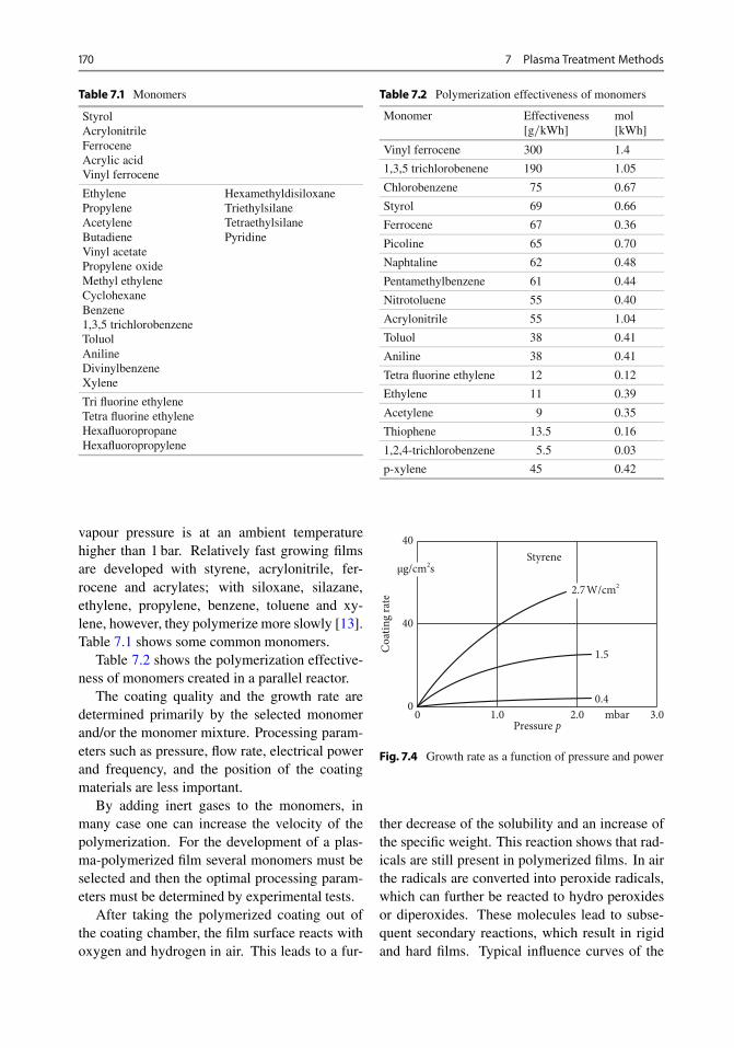
170 7 Plasma Treatment Methods
Table 7.1 Monomers
StyrolAcrylonitrileFerroceneAcrylic acidVinyl ferrocene
EthylenePropyleneAcetyleneButadieneVinyl acetatePropylene oxideMethyl ethyleneCyclohexaneBenzene1,3,5 trichlorobenzeneToluolAnilineDivinylbenzeneXylene
HexamethyldisiloxaneTriethylsilaneTetraethylsilanePyridine
Tri fluorine ethyleneTetra fluorine ethyleneHexafluoropropaneHexafluoropropylene
vapour pressure is at an ambient temperaturehigher than 1 bar. Relatively fast growing filmsare developed with styrene, acrylonitrile, fer-rocene and acrylates; with siloxane, silazane,ethylene, propylene, benzene, toluene and xy-lene, however, they polymerize more slowly [13].Table 7.1 shows some common monomers.
Table 7.2 shows the polymerization effective-ness of monomers created in a parallel reactor.
The coating quality and the growth rate aredetermined primarily by the selected monomerand/or the monomer mixture. Processing param-eters such as pressure, flow rate, electrical powerand frequency, and the position of the coatingmaterials are less important.
By adding inert gases to the monomers, inmany case one can increase the velocity of thepolymerization. For the development of a plas-ma-polymerized film several monomers must beselected and then the optimal processing param-eters must be determined by experimental tests.
After taking the polymerized coating out ofthe coating chamber, the film surface reacts withoxygen and hydrogen in air. This leads to a fur-
Table 7.2 Polymerization effectiveness of monomers
Monomer Effectiveness[g=kWh]
mol[kWh]
Vinyl ferrocene 300 1.4
1,3,5 trichlorobenene 190 1.05
Chlorobenzene 75 0.67
Styrol 69 0.66
Ferrocene 67 0.36
Picoline 65 0.70
Naphtaline 62 0.48
Pentamethylbenzene 61 0.44
Nitrotoluene 55 0.40
Acrylonitrile 55 1.04
Toluol 38 0.41
Aniline 38 0.41
Tetra fluorine ethylene 12 0.12
Ethylene 11 0.39
Acetylene 9 0.35
Thiophene 13.5 0.16
1,2,4-trichlorobenzene 5.5 0.03
p-xylene 45 0.42
40
μg/cm2s
Coa
ting
rate
40
00 1.0 2.0
Styrene
0.4
1.5
2.7W/cm2
Pressure pmbar 3.0
Fig. 7.4 Growth rate as a function of pressure and power
ther decrease of the solubility and an increase ofthe specific weight. This reaction shows that rad-icals are still present in polymerized films. In airthe radicals are converted into peroxide radicals,which can further be reacted to hydro peroxidesor diperoxides. These molecules lead to subse-quent secondary reactions, which result in rigidand hard films. Typical influence curves of the

7.2 Plasma Diffusion Treatment 171
5.0
0.1
0.5
0.5
1.0
mg/hr cm2
Aver
age c
oatin
g ra
te
1 5 10
100% Conversion
Film
Film
Bell-Jar-reactor
Pipereactor
Film and powder
50N cm3/min
p= 2mbarp/A = 0.55W/cm2
Monomer flow rate100
Fig. 7.5 Growth rate as function of monomer gas flowfor two different reactor types (pressure 2.5 mbar, power0:55W=cm2)
parameters pressure, power, flow and frequencyare shown in Figs. 7.4 and 7.5.
The growth rate rises with increasing pressureand plasma power, the film quality is reduced upto an optimum. This is only valid for the flow(Fig. 7.5).
Figure 7.6 shows the influence of the fre-quency. However, we should not only see thegrowth rate but we should also consider the filmquality and the process engineering aspects ofthe different frequency ranges. The parameterflow rate, pressure and electrical power feed intothe plasma are plotted in characteristic curves inFig. 7.7.
7.2 Plasma Diffusion Treatment
The industrial use of the plasma diffusion treat-ment methods began in the sixties. Today ni-
Fig. 7.6 Growth rate ofethylene as a function of thedischarge frequency
4
2
6μg/cm2min
Gro
wth
rate
0Frequency
Hz106105104 107103102
4
3
2
5
mbar
Pres
sure
p
1
00 10 20202020
Lubricious filmUnstabledischarge
Film
Solid film
Film andpowder
100W50W
Ethylene flow rate70N cm3/min
Fig. 7.7 Characteristic curves of plasma polymerizationof ethylene
trogen, carbon, boron and metallic alloying el-ements can be diffused with diverse proceduresinto the edge zones of workpieces. A classifica-tion of plasma diffusion treatment in relation toother plasma procedures is shown in Fig. 4.1.
7.2.1 Description of theMethod
The principle of the plasma diffusion method isshown in Fig. 7.8.
The workpieces that will be treated are iso-lated by being hung up at a charge rack, whichlocks in a recipient. The recipient is evacuated upto a pressure of 1 to 5 mbar. Between the chargerack and the recipient wall an electrical DCvolt-age between 300 to 600 V is applied, so that theprocess gas is ionized in the recipient. A glowdischarge is develops. The charge rack potential

172 7 Plasma Treatment Methods
Gas
Pump
Control system
Heating
Pulseplasma
M
M
Vacuum chamber
Process temperature
Pressure
Wall temperature
Fig. 7.8 Schema of equipment for plasma diffusion treatment with a cold wall recipient
Fig. 7.9 a Potentialprocess between anode(recipient), b glow dis-charge on a workpieceand cathode (workpiece),Up process voltage,Uk: cathode fall
Cathodea b
U = OV
– Up
– Uk
Negative glow lightCathode fall
Anode
is negative. Positive ions are accelerated to thecharge rack. In the range of the cathode fall ofthe glow discharge the work piece contours willbe post-formed very well (Fig. 7.9).
The positive gas ions take up kinetic energywhen they fly through the cathode fall and impactthe surface of the workpieces. The energy that istransferred thereby leads to heating of the work-pieces. Depending on the process gas mixture,the chemically reactive ions and excited atomsexecute a chemical interconnection with the ma-terial of the workpieces. As a function of theworkpiece surface temperature, particles diffuseinto the substrate material. During the treatmentprocess the process gas pressure must be heldconstant in the recipient. For nitrating or nitro-carburizing nitrogen and hydrogen gas mixtures,ammonia and/or nitrogenous gases with carbon
additives such as methane are used with the mate-rial of the workpieces [14–16]. In the range of theoutermost edging zone of the workpiece it comesto formation of a diffusion zone or to enrichmentwith nitrogen and/or carbon.
7.2.2 Fundamental Processes
The fundamental interaction processes betweenmaterial surface and plasma are described inFig. 7.10 .
Thereby the following processes occur:� Heating of the workpiece� Dislodge of atoms from the surface, whereby
impurities of the surface are removed� Penetration of gas ions into the workpiece sur-
face

7.2 Plasma Diffusion Treatment 173
Cathode Anode
ElectronAtom
Fe
Fe
FeN
FeN
Fe2N
Fe3N
Fe4N
N2
N
N CO
Adsorption
ε-Phase
γ-Phase
α-Phase
Furn
ace w
all
Wor
k pi
ece
N
N
N
N
Fig. 7.10 Interaction processes between workpiece sur-face and plasma
� Release of electrons necessary for the furtherexistence of the independent gas discharge.
7.2.3 Correlations Between DifferentPlasma Parameters
Aspects of plasma diffusion treatment are as fol-lows:� The ranges of voltage and current density for
the perpetuation of an abnormal glow dis-charge are small. They depend on:– stability of the plasma– development of sparking.
� The current density in the plasma on the work-piece surface is large, which means:– Intense heating of the workpieces, in par-
ticular with a large surface/volume rela-tionship
– Intense sputtering of the workpiece surfaceby ion bombardment.
VSDS
1200
1000
800
600
400
200
1400
0
Har
dnes
s HV
0.2
0 0.6 mm0.40.2 0.8Distance from surface
X 35 CrMo 17 (1.4122)
34 CrAlNi 7 (1.8550)
X 40 CrMoV 51 (1.2344)
Fig. 7.11 Plasma of edge zones of nitrated workpiecesfrom steel with the hardness–depth profile
� The expansion of the glowing corona aroundthe workpieces is low, which means:– Good post-forming by complex workpiece
geometry– Good penetration in holes and screw
threads of workpieces.At the start of the process one begins withlow temperature at low pressure. If the work-pieces are heated only by the glow discharge, theheating-up time is long. To increase the temper-ature of the work pieces the gas pressure in therecipient is increased. The transition of the ele-ments in the process gas to the material inside theworkpiece is not yet completely resolved. Somemodels explain some phenomena, however con-tradictions due to experimental results remain.The model of Kölbel [17] is commonly used.
Figure 7.11 shows the curves of the hardness–depth profile of different samples from alloyedsteels [18–20].

174 7 Plasma Treatment Methods
Table 7.3 Comparison of different plasma-supported diffusion procedures for the treatment of steel
Plasma diffusionmethod
Applicator gas Treatmenttemperature
Time oftreatment
Separation layer Depth ofdiffusion
(ıC) (h)Sort Thickness
(µm) (µm)
Nitrogen hardening NH3, N2 300–600 0.2–100 Fe4N,Fe2–3N
0–10 100–800
Nitro carbonization NH3, N2,C CH4, CO2
500–600 0.5–30 Fe4N 2–20 100–800
Carbonization CH4, C3H8 800–1000 0.5–3 – – 500–1500
Carbo nitriding CH4, C3H8,C N2
800–1000 0.5–3 – – 500–1500
Borating BCl3, BF3,B2H6
800–1000 1–10 FeB,Fe2B
20–200 100–1000
Alloying Al-, Cr-, Mo-,Ti-, W-Steam
900–1050 3–6 – – 10–300
Table 7.4 Relation of different plasma-supported diffusion procedures for treatment of nonferrous metals
Plasma diffusionmethod
Applicator gas Treatmenttemperature
Time oftreatment
Separation layer Depth ofdiffusion
(ıC) (h)Sort Thickness
(µm) (µm)
Nitrogen hardeningof titanium
N2 800–1000 1–20 TiN 1–5 20–80
Nitro carbonizationof titanium
N2, CH4 800–1000 1–20 TiC-N 1–5 20–80
Carbonization oftitanium
CH4, C3H8 800–1000 1–20 TiC,a–C
1–5 20–80
Nitrogen hardeningof aluminium
NH3, N2 450–500 1–10 AIN 1–5 1–5
7.2.4 Plasma Nitration of Titanium
In order to apply wear-resistant titanium nitridefilms on titanium surfaces, the titanium work-pieces can be directly nitrated in the plasma [21–24]. Because of the large affinity of oxygen, theoxygen content in the recipient must be as smallas possible during the treatment.� The temperatures during the treatment must be
between 800 and 1100 ıC.� The incorporated film thickness reaches val-
ues between 2 and 5 µm.� The diffusion zone is between 20 and 80 µm.� The hardness of the surfaces is appropriate be-
tween 1000 and 2000 HV.
7.2.5 Plasma Nitration of Aluminium
Aluminium alloys are usually made wear-resistant by anodic oxidation at the surface. Thismethod can be substituted by surface nitration.Because of there always exist rugged oxides onaluminium surfaces, nitration without removal ofthe oxides from the substrates is not possible.A method to do this is plasma etching. Thealuminium surface will not be damaged thereby.Aluminium is nitrated at 450 and 500; ıC. Thehardness of the nitrated layer amounts to about1000 HV. The thicknesses of the films reach val-ues between 4 and 5 µm.

7.3 Plasma Spraying 175
7.3 Plasma Spraying
At plasma spraying a powdered coating materialis transferred under use of a plasma flame fromthe solid into the liquid state. Afterwards it isgenerally deposited onto a nonheating substratesurface [25]. The principle of plasma spraying isshown in Fig. 7.12.
The energy source is an electric arc, which isignited by means of a high DC-voltage spark ora high frequency spark. The arc burns betweenintensively water-cooled electrodes, a finger-shaped tungsten cathode and a copper anode aredesigned as a nozzle. The plasma gas is led intothis nozzle, which consists of argon or a mixtureof argon, helium, nitrogen and hydrogen. Theelectrons emitted from the cathode dissociate andionize the gas atoms and gas molecules throughcollisions.
The arc base point rotates due to electrome-chanical effects and so a too high local heating ofcathode and anode is avoided. The arc is con-stricted by thermal effects (thermal pinch) andby its own magnetic field (magnetic pinch) inthe cross-section. At the nozzle opening, af-ter leaving the arc, recombinations of ions toatoms and molecules in the plasma take place.By the released recombination energy, tempera-tures of up to 20,000 K arise in the core of theplasma. The energy content and the temperatureof the plasma depend on the gas or gas mixtureused. The enthalpy of the monatomic gases ar-gon and helium is substantially lower than thatof the diatomic gases hydrogen and nitrogen. Onthe other hand, the temperature is substantiallyhigher in the plasma than with hydrogen and ni-trogen [26].
With the feed gas stream, powder can be in-jected into the high energy plasma beam. Afterinjection the powder particles are transferred intothe liquid state and accelerated. The axial veloc-ity component of the powder particles dependson the flow rate of the plasma gas and the volu-metric expansion of the gas by the transition tothe plasma. At a high particle velocity the flightphase of the powder particle to the impact on thesubstrate surface is only few milliseconds, on this
Spraying particle not come to adhesion(spraying losses)
Powder inflow Cooling water Plasma gas
Cooling water
Tungsten cathodeCopper anodePlasma inflame
Spraying beam
Spra
yed
coat
ing
Base
mat
eria
l
+–
Fig. 7.12 Principle of plasma spraying
the particles solidify and form gradually a thick,compact bonding coating, Figs. 7.13 and 7.14.
Due to the construction space used for theplasma burner, coatings are possible only onfreely accessible surfaces as well as on rotationsymmetrical components. An internal coating ofpipes with atmospheric plasma starting from aninside diameter of 30 mm is possible, wherebythe coating depth is limited due to the nozzle con-struction. A coating of undercuts is, in principle,not possible.
An advantage of plasma spraying is given alsoby the simultaneous processing of more than onlya powdered material to a film. The differentpowder materials are supplied to the plasma overseparate nozzles [26]. The composition of thepowder substance, and thus the properties of thefilm, can be changed by controlling the process.In order that the plasma-sprayed films adhere tothe workpiece surface, the surface must, for ex-ample, be irradiated with corundum [27].
Plasma spraying is a chaotic process. Themelted powder particles anchor themselves ontothe surface, and with increasing film thicknessinto one another, and with atmospheric plasmaspraying cavities arise. Therefore the treated sur-face has many lattice defects such as dislocations,microcavities or lattice deformations. The meltedpowder particles penetrate because of their highkinetic energy and the capillary effect in uneven-ness and undercuts. There they solidify very fastand it comes to mechanical anchoring. Duringthe coating of metallic materials with metallicbulk material it also comes to metallurgical in-teractions between spraying particles and bulkmaterial. At very high powder particle velocities

176 7 Plasma Treatment Methods
Fig. 7.13 Microscopicallysmall droplet melted coat-ing material
Particle before impact
Heightened edge Melting Melting
Heat flowHeat flow
HeatflowSolid core
Direction of spraying
Fig. 7.14 Development ofa plasma-sprayed layer
Cavity
Oxidizedparticle
Not meltedparticle
Substrate
in a sprayed coating it comes to partial weldingof the spraying particles among themselves. Inaddition, in the transient range between film andbulk material it can also come to microwelding.The effects of interaction can be seen in Fig. 7.14.
7.3.1 Process Variants
The number of variables influencing plasmaspraying is very large. Their interactions are il-lustrated in Fig. 7.15.
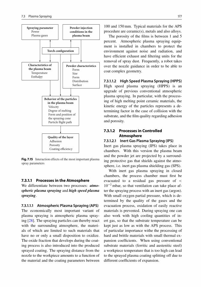
7.3 Plasma Spraying 177
Torch configuration
Powder injectionconditions in the
plasma beam
Spraying parameterPowerPlasma gases
Powder characteristicsFormSizeFormDistributionSurface
Quality of the layerAdhesionPorosityCoating efficiency
Characteristics ofthe plasma beam
TemperatureEnthalpy
Behavior of the particlesin the plasma beamVelocityDegree of meltingForm and position ofthe spraying coneParticle flight path
Fig. 7.15 Interaction effects of the most important plasmaspray parameters
7.3.1.1 Processes in the AtmosphereWe differentiate between two processes: atmo-spheric plasma spraying and high speed plasmaspraying.
7.3.1.1.1 Atmospheric Plasma Spraying (APS)The economically most important variant ofplasma spraying is atmospheric plasma spray-ing [28]. The spraying particles can thereby reactwith the surrounding atmosphere, the materi-als of which are limited to such materials thathave no or only a small disposition to oxidize.The oxide fraction that develops during the coat-ing process is also introduced into the producedsprayed coating. The spraying distance from thenozzle to the workpiece amounts to a function ofthe material and the coating parameters between
100 and 150 mm. Typical materials for the APSprocedure are ceramic(s), metals and also alloys.
The porosity of the films is between 1 and 5percent. Atmospheric plasma spraying equip-ment is installed in chambers to protect theenvironment against noise and radiation, andhave efficient exhaust and filtering units for theremoval of spray dust. Frequently, a robot takesover the nozzle guidance in order to be able tocoat complex geometry.
7.3.1.1.2 High Speed Plasma Spraying (HPPS)High speed plasma spraying (HPPS) is anupgrade of previous conventional atmosphericplasma spraying. In particular, with the process-ing of high melting point ceramic materials, thekinetic energy of the particles represents a de-termining factor in the case of collision with thesubstrate, and the film quality regarding adhesionand porosity.
7.3.1.2 Processes in ControlledAtmosphere
7.3.1.2.1 Inert Gas Plasma Spraying (IPS)Inert gas plasma spraying (IPS) takes place inchambers. With this version the plasma beamand the powder jet are projected by a surround-ing protective gas that shields against the atmo-sphere, i.e. inert gas plasma shielding gas (SPS).
With inert gas plasma spraying in closedchambers, the process chamber must first beevacuated to a residual gas pressure of <
10�2 mbar, so that ventilation can take place af-ter the spraying process with an inert gas (argon).With small oxygen partial pressure, which is de-termined by the quality of the gases and theevacuation process, oxidation of easily reactivematerials is prevented. During spraying one canalso work with high cooling quantities of in-ert gas, so that the substrate temperature can bekept just as low as with the APS process. Thisof particular importance withe the processing ofhard and brittle materials with small thermal ex-pansion coefficients. When using conventionalsubstrate materials (ferritic and austenitic steel)a workpiece temperature that is too high can leadto the sprayed plasma coating splitting off due todifferent coefficients of expansion.

178 7 Plasma Treatment Methods
The process of inert gas jacket plasma spray-ing or shrouded plasma spraying (SPS) does nottake place in a closed chamber. In principle, itis an APS process, by which the plasma beam isprotected by an inert gas flow, which the plasmacoaxially envelopes, and so an interaction ofthe spraying particles and the plasma with thesurrounding atmosphere is prevented to a largeextent. The additional gas flow is not ionized andcools the substrate.
7.3.1.3 Vacuum Plasma Spraying (VPS)With vacuum plasma spraying (VPS) the coatingprocess takes place in a vacuum chamber. Afterevacuating the chamber (pressure < 10�2 mbar)the plasma spraying process in inert gas takesplace at pressures between 50 and 400 mbar. Inorder to keep the pressure in the chamber con-stant, the inflow plasma gases must be exhausted.In the inert atmosphere the liquid spraying par-ticles are protected. An advantage over the APSprocedure is the possibility of using an electricarc for substrate surface cleaning [29].
Because of the larger gas expansion in thevacuum, the plasma beam is more stable be-cause of the weakened interaction effect with thesurrounding atmosphere. The use of a Laval noz-zle amplifies this effect [30]. With the smallernumber of gas molecules in the low pressure at-mosphere the plasma beam becomes longer andthe gas velocity higher than under atmosphericpressure. A turbulence of the plasma beam arisesonly with a larger distance of the nozzle. Thehot zone of the plasma beam thereby becomeslonger [31]. The larger expansion of the plasmabeam is connected with a decrease of the powerdensity.
With vacuum plasma spraying also the ba-sic material is heated to higher temperatures,since the lack of cooling and the smaller num-ber of surrounding molecules means that lesswarmth can be dissipated. In addition, this hasthe advantage that at the lower cooling speedthermal stresses between layer and substrate ma-terial remain small. The higher temperatures alsoincrease the diffusion between layer and basicmaterial, with the result of improved film adhe-sion. The spraying distance with the VPS process
Fig. 7.16 View into the vacuum chamber of two-beamRF-plasma spraying equipment during the manufacture ofYBa2Cu3O7�x-layers
lies between 250 and 350 mm. Films with porosi-ties of less than 1 % are typical.
7.3.1.4 Electrodeless Plasma SprayingElectrodeless plasma spraying was developed forthe production of very pure films. Figure 7.16shows the view inside two-beam equipment forthe deposition of high temperature superconduc-tor films of YBa2Cu3O7 [32]. Argon was used asthe working gas. The pressure during the coat-ing amounted to 4 mbar, the RF-frequency was2 MHz and the power was between 600 W and1.2 kW. The powder stream was about 1 g=minand the gas flow 2 l=min. An advantage overthe RF plasma spraying process is that the powercoupling can be adjusted exactly along the dis-charge tube. The film prosperities can, therefore,be adjusted very exactly.

7.3 References 179
References
1. Hartmann R (1990) Beschichtung durch Plasmapoly-merisation. TECHNIKA 19:151–154
2. Yasuda H (1981) Glow discharge polymerization. In:Journal of Polymer Science: Macromolecular Re-views 16:199–293
3. Linder EG, Davies AP (1931) J Phys Chem 35:3649
4. Gregor LV (1965) In: Thun R, Haas G (eds) Physicsof Thin Films. New York, Academic Press 1065, Bd.3 pp 113
5. Holland L (1956) Vacuum Deposition of Thin Films.Chapman and Hull, London
6. Shen M (ed) (1976) Plasma Chemistry of Polymers.Marcel Deker
7. Shen M, Bell AT (1979) Plasma Polymerization ACSSymposium Series, vol. 108.
8. Hollahan JR, Bell T (eds) (1974) Techniques and Ap-plications of Plasma Chemistry. Wiley, New York
9. Poll HV, Tiller HJ, Wickleder KM (1978) Poly-mere dünne Schichten. In: Hamann G (ed) Organ-ische Festkörper und anorganische dünne Schichten.Akademische Verlagsgesellschaft, Berlin, pp 399–490
10. Poll HV (1970) Zur Angew Phy 29:260
11. Kieser J (1989) Plasmapolymerisation als industrielleinsetzbare Technik. In: VDI-Technologiezentrum(ed) Plasmagestütztes Verfahren der Oberflächentech-nik. VDI Verl. p 106/131
12. Grünwald H (1992) Polymerisation zur Lösung vonAdhäsionsproblemen. In: plasmatec ’92. UniversitätDuisburg
13. Topics in Current Chemistry. Vol. 89 und 90,Springer-Verl. 1980
14. Flis J, Mankowski J, Rolinski E (1989) Corrosion be-haviour of stainless steel after plasma and ammoniacnitriding. Surface Engineering 5(2):151
15. Briglia T, Terwagne G, Bodart F, QuaeyhaegensC, D’Haen J, Stals LM (1996) Study of nitrogen-implanted stainless steels by CEMS and TEM. SurfCoat Technol 80:105–108
16. Berg M, Budtz-JÆrgensen CV, Reitz H, SchweitzKO, Chevallier J, KringhÆj P, BÆttiger J (2000) Onplasma nitriding of steels. Surf Coat Technol 124:25–31
17. Kölbel J (1965) Die Nitridschichtbildung bei derGlimmentladung Forschungsbericht d. LandesNordrhein-Westfalen, vol. 1555. WestdeutscherVerlag, Opladen
18. Dearnley PA, Namvar A, Hibberd GGA, BellT (1989) Some observations on plasma nitridingaustenitic stainless steel Proc. 1st Int. Conference onplasma surface engineering, Garmisch-Partenkirchen.DGM Informationsgesellschaft, Oberursel, p 219
19. Camps E, Muhl S, Romero S, Garcia JL (1998) Mi-crowave plasma nitride austenitic AISI-304 stainlesssteel. Surf Coat Technol 106:121–128
20. Flis J, Mankowski J, Rolinski E (1989) Corrosion be-haviour of stainless steel after plasma and ammoniacnitriding. Surface Engineering 5(2):151
21. Rie KT, Eisenberg S (1987) Mikrostruktur von Titanund Titanlegierungen. Härtereitechn Mitt 42(6):344–349
22. Rolinski E, Karpinski T (1987) Wear Restistance andCorrosion Behaviour of Plasma nitride Titanium Al-loys. Proc. Of the Intern Seminar on Plasma HeatTreatment. PYC Edition, Paris, Senlis/France, pp255–263
23. Souchard JP, Jacquot P, Coll B, Buvrun M (1990)Ionic Nitriding and Ionic Carburizing of pure Tita-nium and its Alloys. Proc of the 2nd Inter. Conf on IonNitriding and Ion Carburizing, Cincinnati, Ohio/USA,1989. ASM
24. Eisenberg S (1988) Plasmadiffusionbehandlung vonTitan und Titanlegierungen. VDI-Verlag
25. Suryanarayanan R (1993) Plasma Spraying: Theoryand Applications. World Scientific Pub Co Inc., p 211
26. Papyrin A, Kosarev V, Klinkov S, Alkhimov A, FominV (2007) Cold Spray Technology. Elsevier, Oxford
27. Lugscheider ER, Agethen R, Knepper M (1989)Löten von Keramik-Metall-Verbindungen durchAufbringen von gradierten Zwischenschichten.Verbindungstechnik in der Elektrotechnik (2):82–85
28. Pawlowski L (1995) The Science and Technology ofThermal Spray Coatings. Wiley, New York
29. Steffens HD, Brandl W, Dvorak M, Wewel M, Rucin-ski D (1991) Vacuum Plasma and Vacuum ArcSprayed Reactive Materials in Comparison. Proc. 2nd
Plasma Technik Symposium, Luzern CH, pp 263–276
30. Jäger D (1989) Spritztechnische Verarbeitung vonRefraktärmaterialien und Refraktärhartstoffen fürKorrosions- und Verschleißschutzanwendungen.Ed.: Lugscheider E, Techn-Wissensch. Berichte Nr.22.19.1.89 1989, RWTH Aachen
31. Heimann RB (1996) Plasma spray coating principlesand applications. VCH, Weinheim, New York, Basel
32. Jäger H, Schulze K, Frey H (1990) Preparation ofYBa2Cu3O7�x Films by Low-Pressure RF-PlasmaDeposition. J. of. The Less-Common Metals, 164 u.165, pp 486–492

8Particle Beam SourcesH. Frey
8.1 Introduction
In this section we consider the fate of energeticions (1–100 keV) incident on a solid surface. The10 ways in which ions can interact with a surfaceare illustrated in Fig. 8.1. An incoming ion canbe backscattered by an atom or group of atomsin the bombarded sample (1). The backscatter-ing process generally results in a deflection ofthe ion’s incident path to a new trajectory afterthe encounter and an exchange of energy betweenthe ion and the target atom. The energy exchangecan be either elastic or inelastic, depending onthe constituent particles and the energy of theions. The momentum of an ion can be sufficientto dislodge a surface atom from a weakly boundposition on the sample lattice and cause its relo-cation on the surface in a more strongly boundposition (2).
This process is called atomic dislocation. Ionswith greater energies can cause internal dislo-cations in the bulk of the sample (3). Physicalsputtering (4) results when ions strike the sam-ple surface and transfer enough momentum toentirely free one or more atom. Ions can pen-etrate into the lattice and become trapped astheir energy is expended (ion implantation) (5).Chemical reaction of the ions with the ions withthe surface atoms can occur, and, as a result, newcompounds can be formed on the sample sur-face, or the outermost layer of atoms may leaveas a gas (chemical sputtering) (6). The bom-barding positive ion can gain an electron fromthe surface by Auger neutralization and be re-
67
8
2
3
5
1
49
10
+
+++
+
+
+
+
+++ +
++
–+
+
12345
Ion-atom scatteringSurface dislocationInternal dislocationPhysical sputteringIon implantation
678910
Chemical sputteringCharge transferIon adsorptionElectron emissionIonized surface atom emission
+
Fig. 8.1 Ion–solid interactions
flected as a neutral atom (7). Ions can becomebound to the surfaces or the sample as adsorbedions (8). Secondary electron emission (9) occursunder suitable conditions of ion bombardment ofmetal surfaces. Secondary ion emission (10) re-sults when surface atoms are excited to ionizedstates and emitted from the sample [1].
Ions are a tool for the modification of filmsnear the surface. This is a very flexible tool dueto the various process parameters of ion radia-tion. These parameters can usually be adjustedindependently and reproducibly, i.e. the tool ofthe ion beam is very well controllable. Because
181© Springer-Verlag Berlin Heidelberg 2015H. Frey, H. R. Khan, Handbook of Thin-Film Technology, DOI 10.1007/978-3-642-05430-3_8

182 8 Particle Beam Sources
of the variety of possible mechanisms of the ionradiation the effects are not predictable in mostcases.
8.2 Basic Processes of Ion–SolidInteraction
8.2.1 Loss of Energy
To analyze the energy loss between two majorenergy loss processes it is convenient to differ-entiate between electronic collisions and nuclearcollisions.
The first process is the interaction of the fastion with the lattice electrons, resulting in exci-tation and ionization. Since the density of theelectrons in the target is high and the collisionsare so numerous, the process, similarly to theelectron energy loss, can be regarded as contin-uous.
The nuclear loss results from collisions be-tween the screened nuclear charges of the ionand the target atoms. The frequency of thesecollisions is lower, so they may be describedby elastic two-body collisions. At high ener-gies they are accurately described by Rutherfordscattering [2], at medium energies by screenedCoulomb scattering, while at low energies the in-teraction becomes even more complex.
In addition, there is a contribution to the en-ergy loss resulting from the charge exchangebetween the moving ion and target atom [3]. Thisenergy loss reaches a maximum when the relativevelocity is comparable to the Bohr electronic ve-locity .2 � 106 m s�1/. The total energy loss –dE=dx can thus be regarded as the sum of threecomponents, nuclear, electronic, and charge ex-change,
dE=dx D .dE=dx/nC .dE=dx/eC .dE=dx/ch :
(8.1)At low ion energies nuclear stopping dominatesand is responsible for most of the angular disper-sion of an ion beam. At high energies electroniccollisions are more important. A useful rule ofthumb is that the energy < lost to the lattice bynuclear collisions becomes predominant at en-
Ion energy (E) - keVA (keV)
Ion
ener
gy lo
ss (
dF dZ )
Chargeexchange
ElectronicNuclear
Fig. 8.2 Variation of ion energy loss with ion energy
TargetSecondaryelectrons
X-rays
Photons
IonsI+
e–
Sputteredatoms
Backscatteredions
I+,I°, I–
Elastic
⎧ ⎪ ⎨ ⎪ ⎩
Inelastic
⎧ ⎪ ⎨ ⎪ ⎩
Fig. 8.3 Schematic representation of ion–target interac-tions
ergies less than A keV, where A is the atomicweight of the incident ion. At intermediate en-ergies the charge-exchange contribution may riseto roughly 10 % of the total. The variation of theenergy loss with ion energy is shown in Fig. 8.2.
Inelastic interactions with the target electronslead to secondary electron emission, emission ofcharacteristic X-rays, and optical photon emis-sion; elastic interactions lead to the displacementof lattice atoms, the formation of defects, and sur-face sputtering, as is illustrated schematically inFig. 8.3.
The energy spectrum of ions [4] with initialenergy E0 scattered from a solid target is repre-sented schematically in Fig. 8.4. There is a broadlow-energy hump (10–30 eV) corresponding tothe emitted neutral atoms (sputtered atoms) anda high-energy hump distributed about the inci-dent ion energy E0 (elastically scattered ions).
If we assume that independently nuclear andelectronic interaction occurred, the entire stop-ping cross-section consists of an electronic part

8.2 Basic Processes of Ion–Solid Interaction 183
Fig. 8.4 Energy spectrumof ions scattered froma solid target
Ion energy - eV
Electronic losses„Nuclear“ losses
50 500 E0 - 50 E0
Inte
sity
- arb
itray
uni
ts
Sputteredparticles
Mainlyneutral
1/E2Multiplescatteredparticles
Ionizationexcitation
Backscatteredions
and a nuclear part:
S D Se C Sn : (8.2)
Both parts can be calculated from the differen-tial effective cross-section of the single scatteringprocess, which depends on the energy transfer �e:
S DZTe d : (8.3)
For nuclear interaction the energy transfer is:
Tn D 4m1m2
.m1 Cm2/2E sin2
�s
2
�; (8.4)
whereby s is the deflection angle (in the grav-ity center system),m1;2 the masses of the nucleus(the indices 1 and 2 designate the projectileand the collision partner). The nuclear collisioncross-section can be calculated from the laws ofclassical mechanics for interatomic interactionpotential. An overview is given in [5]. Such po-tentials can be written in the form of a shieldedCoulomb potential
V D Z1Z2e2
4�"0r�� ra
�; (8.5)
with the nuclear charge numbers of Z1;2, the in-ternuclear distance r , the shielding function �,and the shielding length ˛. For analytic calcula-tions it is meaningful to use universal approxima-tions.
The shielding length after Lindhard et al. [6]for the Thomas Fermi potential � D �TF can becalculated in accordance with
aTF D 0:8853 a0�Z
23
1 CZ23
2
� 12
; (8.6)
whereby a0 is the first Bohr radius a0 D 5:59 �10�9 cm.
With new systematic calculations for manyion–atom interactions [6] a universal shieldingfunction can be written as an exponential series:
�U.y/ D 0:182e�3:2y C 0:51e�0:942y
C 0:28e�0:403y C 0:0282e�0:202y ;(8.7)
with the universal shielding length
aU D 0:8853 a0
Z0:231 CZ0:23
2
: (8.8)
For the universal calculation of the stopping datawe use dimensionless variables for the energy[7]:
" D 4�"0am2
Z1Z2e2.m1 Cm2/E (8.9)
and the distance
% D �a2n 4m1m2
.m1 Cm2/2x : (8.10)

184 8 Particle Beam Sources
The reduced nuclear stopping power fora Thomas Fermi potential is in good approxi-mation given by [8]
��
d"
d%
�
n
D 3:44p" log."C 2:718/
1C 6:35p"C ".6:882p" � 1:708/ :(8.11)
The electronic deceleration must be treatedquantum-mechanically for high projectile veloc-ities. In the Thomas Fermi model
v D v0Z23
2 ; (8.12)
whereby v0 D c=137 is the velocity of the elec-trons at the first Bohr’ orbit (velocity of light).
For the Bethe formula we obtain [9]:
S>e D2�Z2
1Z2e4
.4�"0/2m1
me
1
Elog
�4me
m1
E
I
�:
(8.13)In Eq. (8.13) e is the elementary charge, me themass of the electron, and I the average ionizationpotential.
For the other limiting case of small velocities,Lindhard and Scharff [10] found by means ofthe classical scattering theory of electronic stop-ping power, with the projectile velocity v Dp2E=m1 proportional to the electronic stopping
power,
S<e D2e2a0
"0
Z7=6
1 Z2
.Z2=3
1 CZ2=3
2 /3=2
v
v0: (8.14)
The intermediate range of average velocitiesis only partly understood and thus describable.Therefore from an interpolation formula we use
1
SeD 1
S<eC 1
S>e; (8.15)
with S<e �pE and S>e � E�1 logE, as given
in Eqs. (8.13) and (8.14).Semi-empirical fit functions describe the elec-
tronic stopping over large energy ranges and formany ions and substances [7–10].
1 keVEnergy
103
Stop
ping
cros
s sec
tion
(10–1
4 eV cm
2 )
N Ti
H Ni
5
4
3
2
1
03
2
1
0
Fig. 8.5 Contributions to the stopping cross-section fortwo different projectile target combinations. Low-energyelectronic stopping (Eq. (8.14), continuous line), high-energy electronic stopping (Eq. (8.13), broken line),nuclear stopping (Eq. (8.11), dashed line), electronic stop-ping after Anderson and Ziegler (dash-broken line)
Figure 8.5 shows the theoretical forecastsfor two ion material combinations. For hy-drogen in nickel the semi-empirical adaptionafter Andersen and Ziegler [11] is shown inFig. 8.5.
For the lightest ions the nuclear part of thestopping is negligible; it dominates for mod-erately heavy ions up to energies of approx-imately 10 keV. The ion stopping was onlyconsidered simple in monatomic species. Inmulti-component materials it can be accepted ap-proximately that ion stopping is not influenced bychemical effects.
For a substance of two elements AyBz Bragg’srule of summation of the stopping cross-sectionis valid:
SAy BzD ySA C zSB : (8.16)

8.2 Basic Processes of Ion–Solid Interaction 185
E0
α
Rp
R⊥
Fig. 8.6 Schematic representation of the ion trajectoryand the average ranges
From the literature there are well-known mate-rials that have intense covalent bounds; thosefrom Bragg’s rule deviate by up to 40 % [10–16].Examples are oxides, carbides, and amorphoushydrocarbons films.
8.2.2 Range Distances
If the total stopping cross-section S is well-known, the average total path of an ion with theinjection energy E0 can be calculated in accor-dance with
Rt D 1
n
E0Z
0
dE
S.E/: (8.17)
Because of the statistic nature of multiple scat-tering a probability can be defined for eachindividual ion. The ions are stopped withina discus-shaped spatial distribution, then their av-erage projected distance is defined after Fig. 8.6.
For heavy ions in light substances multiplescattering is small. In raw approximation andin the energy range, in which electronic stoppingcan be neglected, the ratio from total distance to
105
102
10–1
10–3 1031Energy
Rang
e (nm
)
keV
Ti Ni
Fig. 8.7 Total distance of titanium ions in nickel (solidline) and projected distance after Eq. (8.19)
projection range in case ofm1 � m2 [17] is valid:
Rt
Rp� 1C m2
3m1
: (8.18)
For light ions Schiøtt [18], assumed that elec-tronic stopping dominates � < 1,
Rt
Rp� 1
�.1 � 2�/ I � D m1
m2
Se.E0/
Sn.E0/: (8.19)
For many ions within the beam spot an implanta-tion zone results around the average implantationdepth R?; for those in the case of an inclined ionincidence the average projected range in accor-dance with (Fig. 8.3) is
R? D Rp cos.˛/ : (8.20)
Relationships become more complicated whenfor light ions in heavy substances, particularlywith small energy or even injection, a large partof the ions are out-scattered (reflected) from thesurface. Figure 8.7 shows the total and projecteddistances (after correction Eq. (3.19)) for tita-nium in nickel.
The treatment for small energies is particu-larly problematic. Distances in about 1 Å arephysically absurd. The principle of the averagedistance becomes irrelevant by strong multiplescattering in connection with ion reflection.

186 8 Particle Beam Sources
I
Z
K
V
R
Rp
Fig. 8.8 Schematic representation of the effects of nu-clear collisions by an incident ion that stopped at theplace R and its projected distance Rp. In the collisioncascade K dislocations .V / and sputtering incidence .Z/can take place
8.2.3 Collision Cascadesand Radiation Damage
The effect of an incident ion on the atoms of theirradiated material is illustrated schematically inFig. 8.8.
Along the path the ion will transfer the energy�n by elastic collisions after Eq. (8.4). The bind-ing energy of an atom in its lattice is some eV;therefore the atom strikes out with very soft col-lisions at its place. Then it can be regarded asa fast particle. If its initial energy �n and distanceis sufficient low, it will return through elastic in-teraction with the lattice to its place. In order toproduce a stable defect, a Frenkel pair from aninterstitial atom and a lattice vacancy, and thresh-old energies from � 10 to 50 eV are necessary.With crystalline materials this threshold energydepends on the direction of the impacted atom.
With high energy transfer a primarily adjoin-ing atom can produce a collision cascade andmore stable Frenkel pairs by further collisions.Using the approximation (Fig. 8.8) the powerdensity is relative low, so that fast atoms essen-tially only collide with resting atoms.
Within this range of the so-called linear cas-cade the number of Frenkel defects per pri-mary collision results when using the modified
Kinchin-Pease formula [22]
vF.Tn/ D
8ˆ<
ˆ:
0 forTn < Ed
1 forEd < TnI T �n < 2:5Ed
0:8
2EdT �
n forT �n > 2:5Ed :
(8.21)T �
n is that part of the primary energy transfer,which is not dissipated by the electronic in-teraction effect.
T �n � 0:9Tn is a good approximation for light
to moderately heavy ions [23]. No defects arecreated, if the energy is so small that at a cen-tral collision the minimum dislocation energy isexceeded. This is about half as large as the ef-fective dislocation energy in raw approximation.Thus we obtain the threshold energy for the gen-eration of defects:
Es0 �
Ed
2�; (8.22)
whereby � is the energy transfer function (seeEq. (8.4))
� D 4m1m2
.m1 Cm2/2: (8.23)
At very high densities for the deposited energythe model of the linear cascade is no longer valid(typically for heavy ions with energies around100 keV). Ranges develop that contain onlyfast atoms, which collide among themselves andoccur during a short time in a thermalized ensem-ble.
In a simple model of this heat pulse (ther-mal spike) [24–26] we assume a straight iontrajectory, along which the energy is deposited ina line shape. From the theory of heat conduction,for the temporal temperature gradient in the dis-tance r from the ion trajectory we have:
T .r; t/ D nSn
4��texp
��%cr
2
4�t
�; (8.24)
whereby � designate the heat conductivity; � thedensity, and c the specific warmth of the targetmaterial. The number of dislocations per ion isaccordingly
dNd
dxD k n2S2nv0
24�E2d�
; (8.25)

8.2 Basic Processes of Ion–Solid Interaction 187
a b c
Fig. 8.9 Schematic representation of the different elementary processes of atomic mixing by ion bombardment. a Col-lisions with marker atoms, b collisions with matrix atoms, c cascade mixing
whereby v0 � 1013=s is a typical frequency ofthe lattice vibrations.
In metals the maximum concentration ofFrenkel pairs lies at some 10�3. Further Frenkelpairs are stable only at very low temperatures ifboth the interstitial atoms and the lattice vacancyare immovable. In insulators the electronic in-teraction can also contribute substantially to thecreation of radiation damage [27, 28].
8.2.4 IonMixing
The ion mixing is based on the spatial dislocationof atoms within a collision cascade. Several pro-cesses contribute to mixing by nuclear collisions(Fig. 8.9).
Sigmund and Grass-Marti [29] found the fol-lowing for cascade broadening:
˝2 D 2�
�2˛
�m2
m1
�Sn.E/
.R.Ee//2
Ee˚ ; (8.26)
where E is the average energy of the ions at theplace of the marker atoms, Ee the minimum en-ergy of an atom for the dislocation, and R .Ee/
the assigned average distance. Ee is generallysignificantly lower than the dislocation energyEd for the creation of a Frenkel pair, if thebulk material is already strongly damaged withhigh bombardment fluencies. Ion mixing can be
affected by further temperature-dependent pro-cesses. Such processes are chemical in nature inconnection with the thermodynamics of the mate-rial mixture [30], or correlated with the mobilityof defects [31].
8.2.5 Irradiation Amplified Diffusion
By a solid body we distinguish, in principle, twomechanisms of mass transport. Foreign atoms,which are located at interstitial locations, canmigrate at sufficiently high temperature betweenthese locations. The diffusion of foreign atomson lattice sites and thus the self-diffusion of thematrix atoms require the presence of lattice va-cancy, which by their migration exchange placeswith the atoms. For both processes a diffusioncoefficient can be indicated as a temperature-independent factor D0 and an activation energyUm
D D D0e� Um
kT : (8.27)
In the simple model for stochastic migration wecan write:
D0 D v0d2
6; (8.28)
whereby v0 indicates the oscillating frequency inthe lattice .� 1013=s/ and d the hopping width ofa single atom.

188 8 Particle Beam Sources
The activation energy for interstitial latticediffusion generally has values in the order of1 eV. For the lattice vacancy mechanism the acti-vation energy is the sum of lattice vacancy energyof formation and lattice vacancy migration en-ergy Um D MUf C MUm, which typically have someeV. The lattice vacancy mechanism begins innon-irradiated material only at very high temper-atures, if sufficient lattice vacancies are producedin the thermal way.
In a general definition we are speaking ofradiation-increased diffusion if the internal ma-terial transport in relation to thermal transportis increased by irradiation. Ion beam mixingcan, therefore, also be regarded as a radiation-increased diffusion. Further, in particular forinterstitial atoms, thermal diffusion induction ofa thermal pulse of an ion can be increased tem-porarily, which leads to an intensified diffusion.The lattice vacancy mechanism thereby playsa substantial role; its activation energy is thenonly given by the migration energy of the latticevacancy (about 1 eV).
In the case of irradiation, the balance equa-tions of the defects (ci;v and Di;v atomic concen-trations and diffusion coefficients of the intersti-tial atom .i/ and the lattice vacancy .v/) are:
@ci
@tD Di
@2ci
@x2�4� Di aivn ci cvCFd.x/ (8.29)
and
@cv
@tD Dv
@2cv
@x2� 4� Di aivn ci cv C Fd.x/ :
(8.30)aiv � n�1=3 is the critical distance for recombi-nation of interstitial atoms with lattice vacancyand Fd the local production rate of Frenkel pairs.
The boundary conditions are: ci.x D 0/ Dcv.x D 0/ D 0 D ci.x ! 1/ D cv.x !1/ at the surface and deep in the bulk material;neglected are internal sinks such as dislocationsor vacancy lattice complexes.
The migration of interstitial atoms at suf-ficiently low temperatures occurs substantiallyfaster than with those of the lattice vacancy.Except within fewer atomic layers in the proxim-ity of the surface the recombination with lattice
vacancies is very probable due to their high con-centration. Interstitial atoms in the bulk materialhave a higher probability of survival. Thus bothdefect types contribute to the intensive, longranges of diffusion. To date there is neithera model nor a calculation method to describe theprocedures completely.
8.2.6 Surface Textureand GrowthMode
The morphology of an increasing film is substan-tially determined by surface processes. Surfacedefects and irregular packing growing into thefilm can be neutralized partly by ion bombard-ment.
The particle energies E are indicated in unitsof the Lennard Jones potential depth " and havevalues between 0.1 eV up to some eV. Thermaloscillations were not considered.
A defect-free film (Frank van der Merwe-growth) morphology with layer on layer growthdepends on the energetic bombardment withions. Without bombardment, however, a mor-phology with many cavities (Volmer-Weber-growth) results from rather an island-like growth(Fig. 8.10). This effect of the ion bombardmentbecomes explicit, if more realistic conditions areused. Figure 8.11 shows the results of simula-tions for ion beam deposition of silver layers atdifferent energies [33].
The increased tendency to Frank-van-der-Merwe growth under ion bombardment is shownby experimental results [34]. It is based on thefact that the ion beam, on the one hand, increasesthe nucleus density and, on the other hand, dis-solves again by lateral dislocation islands. This isrepresented schematically in Fig. 8.12. Both par-tial mechanisms require the creation of surfacedefects.
After this conception if a defective-free mor-phology is to be possible, for example at epitaxialgrowth, the generation of surface defects shouldbe maximized, while volume defects should beminimized at the same time. Quantitatively thisview was examined in various observations of the

8.2 Basic Processes of Ion–Solid Interaction 189
a
b
c
E = 0.05 ε
E = 0.03 ε
E = 0.15 ε
Fig. 8.10 Two-dimensional molecular-dynamic simula-tion of film growth by atomic deposition with the help ofa Lennard Jones potential [32]
ion bombardment by silicon and germanium withdifferent ions [35].
Quantitatively this view was examined in var-ious observations of ion bombardment by siliconand germanium with different ions [35]. Fig-ure 8.13 shows isocontour lines for constantrelationship from surface dislocations to volumedislocations for different ion energies and ionmasses.
This relationship becomes infinitely large dur-ing the approach to the effective volume disloca-
a b
Fig. 8.11 Molecular-dynamic simulation of the growth ofsilver layers at ambient temperature with an EAM poten-tial for incidence energies of 0.1 eV (a) and 10 eV (b)
a b
Thermally IBad
Fig. 8.12 Schematic representation for the suppression ofisland growth by ion bombardment
100
10
1000
amu
1100
Ion energy
Ion
mas
s
Nominal volumethreshold
Surfacethreshold
Effective volumethreshold16
40 8 4 1.6 0.8
0.4
R = 0.2
Si
eV10 1000
Fig. 8.13 Isocontour lines of the relationship R of sur-face defects to volume defects as function of ion energyand ion masses for the bombardment of silicon. Furthervolume thresholds and surface thresholds are drawn
tion threshold energy. The threshold energy after(8.22), calculated for surface dislocation energywas accepted to be half as large as the volumedislocation energy.

190 8 Particle Beam Sources
c
b
d
a
Fig. 8.14 Molecular-dynamic simulation of the integra-tion of an energetic molybdenum cluster into a molyb-denum layer. The energy of 5 keV distributes itself on1024 atoms of the cluster. The time differences betweenthe snapshots of simulation amount to b 2.25, c 9, and d17.25 ps [37]
With ion energies under the effective volumedislocation threshold only surface dislocationsare created, until finally, with very low energies,no more dislocations are possible. The formof the isocontour lines and limiting curves re-sult from the energy transfer of the incident ion(Eq. 8.4) on the silicon target atoms. The gen-eral trends of this model were also confirmed bymolecular-dynamic simulations for silicon lay-ers [35].
New aspects for modeling of film growthbring in the deposition by energetic ionized clus-ters [36]. With clusters of the order of magnitudeof 1000 atoms, with high particle energies of sev-eral keV, incidence energies between 1–10 eV peratom can also be obtained (Fig. 8.14).
The cluster first penetrates with very hightransient temperatures and pressures into the sur-face and thereby spreads out laterally. A film ofapproximately 10 atoms thick on the substrateis initially disturbed. It is hoped to get a filmwith a good epitaxial property, a sufficient mix-ture with the basis, and only low defects in thefilm and in the substrate. This simulation quali-tatively agrees with experimental analyses.
Ion bombardment
Den
sity
Stre
ssM
orph
olog
y
Poro
us
Vaca
ncy
defe
ct
Idea
l
Idea
l
Inte
rstit
ial a
tom
s
I II III IV V
Tension
Compression
p0
0
Fig.8.15 Schematic representation of the relationship be-tween film morphology, density, and internal stress asa function of ion bombardment
8.2.7 Density and Stress
With the model of Thornton, Fig. 6.15, it be-comes explicit that ion bombardment affects themorphology and the density of the film. Fig-ure 8.15 shows a qualitative pattern for lowsubstrate temperatures. Without ion bombard-ment (regime I) a vapor-deposited or a sputteredfilm becomes porous. Their density is relativelylow: the porous structure can only take absorbstresses.
With increasing ion bombardment (increasingion energy or a higher ion/neutral relationship)the cavities are filled, so that there remain espe-cially small lattice vacancy clusters or a singlelattice vacancy: an internal tensile stress devel-ops. With increased ion bombardment, atomsthat are displaced from the surface in the vol-ume fill the lattice vacancy (regime III), sothat with determined conditions the ideal den-

8.2 Basic Processes of Ion–Solid Interaction 191
sity of the unstressed material results. Accord-ingly, highly strengthened bombardment pref-erentially leads to interstitial atoms (or loweraccumulations of interstitial atoms) and thusto increased density and internal compressivestress.
At relative low energies, up to a few 10 eV,within the ranges I–IV there are especially sin-gle collision processes. It is only with higherenergies in regime V that it comes to extendedcascades, within those by dislocation or reco-ordination of interstitial atoms the compressionstrength is reduced and the density decreased.The dependence of tension with the use ofion bombardment is semi-empirically describedin [38].
The range III with the structure of compres-sive strengths during the film deposition is de-scribed by sputtering [38]. The relative volumevariation, which is connected over Hooke’ lawwith the tension, is assumed proportionally to thedislocation rate. The latter is calculated similarlyas with Sigmund sputtering theory.
For the tension in the film we obtain
S D C j E1=2 M
1 � v ; (8.31)
wherebyC indicates a constant,J the ion flux,E the ion energy,M the modulus of elasticity, andv the Poisson number.The transition from regime IV to regime V ischaracterized by the fact that interstitial atomsare deposited by direct implantation or recoil im-plantation, but compete by dislocation or struc-tural change in expanded collision cascades to beagain removed. A simple analytic model of thesupplantation can be determined from the fluxbalance. For an ion beam sputtering process itis assumed that a fraction P (probability of pen-etration) of the striking ions penetrates into thesurface and forms interstitial atoms, while theremainder on the surface is deposited and thedensity of the undisturbed material assumed.
For the relationship of interstitial atoms(atomic concentration ci) and lattice atoms (c0)
for an incident ion flux j it is then valid:
ci
c0D j P � j Ycci
j.1� P /C j Ycci; (8.32)
with the conversion rate of yield Yc. From this itfollows that:
ci D 1 � c0 D P
1C Yc: (8.33)
If we continue to assume the fact that interstitialatoms do not cause a distortion then for the re-sulting number density n we obtain:
1
nD c0
n0; (8.34)
whereby n0 is the density of the defect-free ma-terial. Thus it follows that:
n
n0D 1C Ye
1C Ye � P : (8.35)
For approaches for the identification of Ye we usethe model of the thermal pulse in the form ofa point source.
For amorphous carbon we obtain a conversionrate of yield
Ye � 0:016�E0
Ec
�: (8.36)
The results are shown in combination with exper-imental results in Fig. 8.16.
8.2.8 Phases in Material Films
We obtain hard material films with good mechan-ical properties if we prefer deposition processesthat create hard material phases. Tetragonalphases are excellent according to cubic phases(diamond-like carbon, c-BN) and hexagonalphases (graphite, h-BN). The hexagonal phasesare energetically more favorable, so that the de-position requires non-equilibrium processes, forexample, by ion bombardment at low tempera-tures. In all these cases it was found experimen-tally that the part of the tetragonal phase from the

192 8 Particle Beam Sources
3.6
3.2
2.8
2.4
2.010 100 eV 1000
Experiment
Calculation
Energy
Den
sity
g/cm3
Fig. 8.16 Density of an amorphous carbon film as a func-tion of ion energy from experiments and model calcula-tions [39]
energy of the ions depends on striking the sampleduring deposition; we find one for a certain ma-terial and for a certain deposition procedure onlyin each case an optimal ion energy.
8.3 Particle Beam Sources
8.3.1 Ion Beam Generation
In this section, we are concerned with the cre-ation and extraction of ions [40]. We will firstdiscuss the different ways in which ions can becreated and then the properties of ion sourcesused in microelectronic applications. This will befollowed by a discussion of the space-charge ef-fects that play an important role in the ion-beamformation used for ion milling, ion implantation,and ion microscopy.
In general, each application of ion beams re-quires a somewhat different source and set ofbeam parameters. The source performance pa-rameters of greatest importance are the follow-ing:� The ion species produced� The ion current produced by the source� The brightness of the source� The energy spread.
An ion beam consists of a large number ofcharged atoms or molecules, which have approx-imately the same velocity, energy, and direction.Their trajectory can be manipulated due to theircharge by electrical and magnetic fields. Ionbeam technology needs high vacuum or ultra-high vacuum, since otherwise with the scatter-ing with neutral atoms and molecules, the ionmovement with respect to energy and directionchanges or causes a complete deterioration of thebeam.
Characteristic sizes of an ion beam are thestate of charge and energy of the ions as well asthe ion current density and the lateral distribu-tion [41].
To illustrate the different characteristics ofthe ion sources, three classes of ion sources arediscussed below: electron-impact, field-ion, andliquid-metal field-ion sources.
8.3.1.1 Electron-Impact IonizationSources
Electron-impact ionization is the most used tech-nique for generating ions for implantation andion processing. In this ionization process the en-ergy transferred to a molecule from an energeticelectron exceeds the ionization energy Ei, whereEi=e is the ionization potential for that molecule(see Sect. 4.5.4). Electrons for ionization can becreated by thermionic or cold cathode emissionor can result from the discharge itself. Theseelectrons are accelerated by the use of DC or RFfields and confined by the use of magnetic fields.
Energetic electrons can lose energy to gas par-ticles through elastic collisions, the dissociationof gas particles, and the excitation of gas parti-cles. The momentum transfer to the gas particlesis usually negligible because of the large massimbalance; thus the increase in kinetic energyof the gas particles is negligible. When an in-cident (primary) electron has energy in excessof the ionization energy, this excess energy canappear as the kinetic energy of a scattered inci-dent electron, as the kinetic energy of an ejected(secondary) electron, as the multiple ionizationof a gas particle, the excitation of a gas particle,or any combination of these effects.

8.3 Particle Beam Sources 193
10 20 50 102
10–1
103 104
Electron energy (U) eV
0.03
0.20.30.51.0
10
0.05
Xe
HgKr
H2
N2
HeH
AO2,CO,NO
H
HeH2
Ne
N2
Diff
eren
tial i
oniz
atio
n co
effici
ent
(Se)
ion
pair
s/cm
-torr
Fig. 8.17 Differential ionization coefficients Se as a func-tion of electron energy E
The number of ionizing collisions suffered byan electron in passing through a gas per unit pathlength per unit pressure is called the differentialionization coefficient Se; the value of this coef-ficient depends on the electron energy Ee andthe gas species. The differential electron-impactionization coefficients for several gas species areshown in Fig. 8.17. It can be seen that electronswith energies much less than or much greaterthan the atomic and molecular ionization ener-gies do not ionize these particles very effectively;electron energies a few times the ionization ener-gies are optimum for electron-impact ionization.
The number of ions per square centimeter persecond Kni produced by an electron current den-sity j (A=cm2) passing a distance l (cm) througha gas of pressure p (mbar) is given by
Kni D .j � zplSe/=e : (8.37)
As an energetic electron loses energy from ion-izing and scattering collisions, its ionizing ef-fectiveness changes. When its energy decreasesbelow the lowest ionization energy of any atom inthe volume, it no longer causes ionization and iscalled an ultimate electron. Energetic electronscan cause ionization efficiently only if they aremaintained in the ionizing volume for a time longenough for them to lose their energy by ionizingcollisions. A confining force resulting, for ex-ample, from a magnetic field or an oscillating RF
field is often employed to increase the path lengthand electron lifetimes. These concepts are illus-trated in Fig. 8.18a–c.
In the hot and cold cathode ion sources theanode is maintained at a positive potential withrespect to the two end plates, so that electronsemitted by the cathode are injected through theplasma sheath in front of the cathode into a regionwhere the potential varies with both the radial andaxial distances.
The application of an approximately axialmagnetic field prevents the electrons from mov-ing directly to the outer cylinder. In this crossedelectric and magnetic field configuration, theelectrons spiral around the magnetic field linesand oscillate longitudinally. As a result of ion-izing collisions between the electrons and theatoms of the source gas, the plasma will be sup-plied continuously with ions and electrons. Theprimary electrons lose energy and diffuse acrossthe magnetic field lines to the outer cylinder,where they are collected, causing an electric cur-rent to flow from the anode to the cathode. Theplasma essentially fills the discharge chamber. Inprinciple, this discharge mechanism can be usedto ionize any gas (Sect. 4.6).
In the RF ion source the ever-present electronsformed in the discharge tube fill the chamber andform a plasma sheath along the chamber walland the extractor electrode. The wall potentialis given by [42]
Uw D kTe=2e lnfTemi=Timeg (8.38)
for an insulator surface, where Te and Ti are theelectron and ion temperatures, andme andmi arethe electron and ion masses, respectively [43].This wall potential causes the plasma bound-ary S1 to move away from the wall surface S2,as shown in Fig. 8.19.
The measure of plasma withdrawal is givenby �D, where �D is the Debye shielding length(see Sect. 4.3). If an aperture larger than 2 �D
is made in the chamber wall, the plasma willballoon out through this opening, as shown inFig. 8.19a. In the opening of the extractor elec-trode the value of the negative potential applied tothis electrode determines the shape of the plasma

194 8 Particle Beam Sources
Fig. 8.18 Electron-impactionization sources. a Oscil-lating electron impact-ionsource, b cold cathode“Penning source”, c RF ionsource
A+A+
II
AO
B
Cathode
Repeller
Vextr
r
Oscillating electron impact-ion source
e–
Mild iron
Permanent magnet
Gas inlet
Extracting electrode
Ions
Anticathode (Mg)
Anode (Mg)
Cathode (Mg)
Ions
Gas inlet
Coupling loop
Extractingelectrode(Dural)
Focusing lens
RF ion source
Wax seal
Discharge tube(Pyrex glass)
Anode (W)
a
Cold cathode “Penning source“b
c

8.3 Particle Beam Sources 195
Fig. 8.19 Beam extrac-tion from plasma sources.a Separation of plasmaboundary S1 from the wallsurface S2 caused by thewall potential Vw, b plasmaboundary in an ion source
PlasmaS1S2
S1S2
Plasma boundary
Separation of plasma boundary S1 from the wall surface S2 caused by the wall potential VWa
Plasma boundary in an ion source b
+ +
++
+
++
+ +
Plasma
Equipotentials
Extractionelectrode
Ions withrandomvelocities
Plasma sheath iszero equipotential
Ion beam
Plas
ma
d Bombardementchamber
E1
X
E2 E3
Potential distribution betweenalong the extraction grid
Fig. 8.20 Schema of an ion extraction optics with threeelectrodes and the potential distribution .�.x// betweenplasma and bombardment area. Potential distribution be-tween along the extraction grid
surface (Fig. 8.19b) because the plasma boundarymust be an equipotential surface and the normalcomponent of the electric field must be zero. Thismeans that if the negative potential is increased,the plasma surface is forced back so that a curvedsurface will be the ion emitter forming a conver-gent beam of ions.
The shape and position of the ion-emitter sur-face of the plasma are thus dependent on thevalue of the negative potential applied to theextracting electrode. This means that the ion-optical system composed of the extracting elec-trode and the plasma surface can have differentgeometries determined by the value of the nega-tive potential applied to the extracting electrode.This imposes limitations on the extracting volt-age so that the beam intensity cannot be variedbeyond a given value by varying the extractingvoltage.
Under normal operating conditions the shapeof the plasma boundary adjusts itself so that theion extraction rate is equal to the supply rate fromthe plasma. In this case, the extracted ion current

196 8 Particle Beam Sources
Plas
ma
E1 E2
Plas
ma
E1 E2
Plas
ma
E1
Extraction voltage increasing from a to b
E2
Plas
ma
E1 E2
Plas
ma
E1 E2
a b
d e
c
Fig. 8.21 Influence of the extraction voltage on the form of the plasma edge layer and the ion beam. Case c correspondsto the optimal operating point.
density is given by the Child–Langmuir equation:
ji D 4"0=9.2e=mi/0:5.Uext/
1:5=d2 ; (8.39)
where Uext is the extractor potential, d is the ex-tractor electrode–plasma boundary distance, andmi is the ion mass.
Often a third electrode is used, which isagain weakly positive on E2 weakly positive(Fig. 8.20). Thus it can be prevented that elec-trons, which were caught by the space charge ofthe ion beam, flow back into the plasma. Bya suitable choice of the voltage applied at E3, theelectron flux from the beam volume in the plasmaand thus the focusing of the ion beam can becontrolled. The difference of potential betweenplasma or electrode E1 and the extraction elec-trode E2 determine the form of the ion-emittingplasma boundary surface (Fig. 8.21).
At too low extraction voltages a convexboundary surface is formed. The predominantpart of the extracted ion beam in this case strikes
the extraction electrode E2 and sputters it. Theextracted ion current density is smaller than itsmaximally possible value. In the case of anincrease of voltage the beam is ever more fo-cused (Fig. 8.21b), until finally its diameter atthe level of E2 accepts the opening diameter ofthis electrode (Fig. 8.21c) and only very few ionsstrike E2.
The transition from divergent to convergentbeam distribution is accompanied by an appropri-ate change in the form of the ion-emitting plasmaboundary surface. With a further increase of theextraction voltage the plasma boundary surfaceis ever more concave and the ion-emitting sur-face (Fig. 8.21d,e) increases. This process isaccompanied with an increase of the ion currentextracted from the plasma. With further deforma-tion of the plasma boundary a stronger focusingof the ion beam arises, whereby its waistlineis shifted closer to the extraction system, untilfinally it is between the electrodes (e). Under cur-rent increase larger repulsive space charge forces

8.3 Particle Beam Sources 197
r1
D
d
∂
r2
E2E1
Plas
ma
Fig. 8.22 Sectional view by an extraction lens. The sizesindicated determine the perveance of the arrangement
in the beam waistline arise, which lead to anintensified expansion of the beam in the bom-bardment area. Thus, the current density at thesubstrate is, however, again reduced. If the focuslies between the electrodes, then the expansion ofthe beam can already be so large in the level ofE1that a part again strikes E2 and with the now highion energies leads to a substantial erosion of theelectrode material.
The maximal ion current extractable by an ionoptics is limited by its own space charge. Gener-ally, for the space charge-limited total current byan extraction system it is valid that
I D P � U 3=2 ; (8.40)
where P is the perveance of the ion-opticalextraction system and U the ion-accelerating po-tential difference between the starting point of theions and the exit electrode.
If we regard a concentric extraction systemwith round grid openings of suitable size asa spherical sector (Fig. 8.22) with the half open-ing angle ı, then we obtain for the perveance:
P D 8p2
9� �"0
re0
M� 1 � cos ı
F.r1=r2/; (8.41)
PlasmaPlasma
a
PlasmaPlasma
b
Fig. 8.23 Ion extraction with curved grid structures in theform of a spherical recess. a Focusing high current den-sity. b Defocusing low current density
where F.r1=r2/ is a function of the two sphereradii r1 and r2 (as those shown in Fig. 8.22 intabulated form) [44].
For the case represented in Fig. 8.22 for thepotential difference U in Eq. (8.40), it is validthat
U D UP1�E1 C UE1�E2 : (8.42)
The maximally extractable ion current is theproduct of the ion saturation current density jion
from the plasma and the surface A of the re-spective ion-emitting plasma boundary surface.Because of the variation of A with the extractionvoltage U the relationship r1=r2 and concomi-tantly the perveance changes with U . This meansthat the geometry of an extraction system must beadapted to the desired ion current density, ion en-ergy, and beam divergence. Detailed theoreticalviews for the calculation of extraction optics canbe found in [45].
For the generation of a large-scale ion beama large number of grid openings must be used.Large area ion beam sources for thin film tech-nology have the following parameters:� Ion energy: 0.1–20 keV� Ion current density: 0.5–20 mA=cm2
� Energy spread: approximately 10–20 eV� Beam homogeneity: approximately 5 %.In order to keep changes of electrode geome-try as small as possible by thermal deformationduring the operation, extraction grids are madeof graphite or of high-melting metals (Mo, Ta),which are covered with ceramic layers at the sur-

198 8 Particle Beam Sources
a
d
c
b
Fig. 8.24 Large area ion gun [48]. a cathodes, b anode,c two-electrode extraction lattice, d permanent magnets(multipole arrangement)
face. Frequently also extraction arrangements incurved form are used (Fig. 8.23).
Such concave or (convex) formed extractionsystems can then also contribute to the focusing(or defocusing) of ion beams [46]. Electrons in-jected into the ion beam can likewise decreasebeam divergence due to the space charge of theion beams.
Fig. 8.25 Freeman ionsource
Isolator Thermocouple Heater Shield
Heat shield
Filament
Extractiongap
Ion beam
Discharge chamberGas inletHeat shield
8.3.2 Large Area Sources
8.3.2.1 Direct Current Ion Sources
8.3.2.1.1 Ion Sources withHot and Cold Cathodes
Figure 8.24 shows a large area ion source basedon a direct current discharge [47, 48]. The plasmais maintained by means of electrons, which areemitted from glow cathodes.
Behind the anode wall permanent magnetsare arranged in a so-called multipole arrange-ment. Under the influence of crossed electricaland magnetic fields in the wall environment theredevelops a circular electron flux with a drift ve-locity,
�!v D�!E � �!BB2
: (8.43)
This leads to an extension of the electron trajecto-ries and the duration of the stay of the electrons.This increases the probability of the electroncollision ionization of neutral gas atoms in thewall environment. The spatial homogeneity ofthe plasma density in the discharge chamber isthereby improved. The source can be oper-ated with argon at a pressure between 10�3 and10�4 mbar with discharge voltages < 50V.
Low electron energies have the advantage thatonly a few percent of multiply ionized gas atoms

8.3 Particle Beam Sources 199
develop. Despite their simple design, sourceswith hot cathodes have disadvantages, which lim-its their application. Apart from the thermalevaporation of the cathode wire, operation withreactive gas leads to fast deterioration of the cath-odes.
Freeman SourceSimilarly to the source of Fig. 8.24, the Freemansource, Fig. 8.25, is a low-voltage gas dischargewith hot cathodes.
An outer axial magnetic field serves to in-crease the probability of ionization. The ions areextracted not at the end of the discharge cham-ber, but laterally by a slot (e.g. 40mm � 2mm).The accelerating electrode is generally in a largevariable distance of 1 to 3 cm in front of thesource. The ions can be extracted from theplasma with relatively large accelerating voltagesof some 10 kV [49].
Freeman sources are particularly used in ionimplantation equipment. Figure 8.26 showsa source used in high current implantation equip-ment. The source is suitable for the productionof PC and AsC ions. The attainable ion beam
Fig. 8.26 Nova–Freeman ion source
Fig. 8.27 Evaporator equipment for the Nova–Freeman-source (company photo Eaton)
Solenoid
Cathode
Cathode
Cathode
Cylindricalanode
Ion beam Gas inlet
1 cm
Fig. 8.28 Cross-section of a Bethge–Baumann source
currents are, for instance, 10 mA. Figure 8.27shows an evaporator unit for the Nova–Freemanion source.
8.3.2.2 Electrodeless High Frequency IonSources
For operation with long maintenance intervals,electrodeless high frequency or microwave ionguns are better alternatives. With these sourcesalso ions from reactive gases and metals can begenerated.
The Bethge–Baumann source [50] works ac-cording to the Penning principle. Figure 8.28shows a schema of this source.
8.3.2.2.1 Sources with Ring DischargesThe simplest design of electrodeless high fre-quency ion sources by inductive excitation is touse a high frequency ring discharge, Fig. 8.29.

200 8 Particle Beam Sources
b
a
c
dBHf
EHf
Fig. 8.29 Schema of a ring discharge ion source. a Highfrequency coil, b plasma chamber (dielectric), c dischargearea, d two-electrode extraction grid
The plasma chamber consists of a cup-shaped di-electric material, which is surrounded by a highfrequency solenoid. The high frequency axialmagnetic field BHF induces an electrical high fre-quency cyclic field EHF. EHF increases with r .The electrons in the environment of the wall areaccelerated more intensively, they form a torus-shaped plasma density distribution (ring dis-charge). Without collisions with gas particles inthe plasma chamber the electrons in all RF-ionsources have a phase difference of �=2. Theymove in the direction to the electrical field andfrom there in the temporal average, no energy istaken up. Only the phase difference is changedthe electrons taken up from the electrical fieldsufficient energy, in order to maintain by colli-sion ionization the plasma discharge.
Typically used frequencies for sources withring discharge are some 100 kHz up to few MHz.
8.3.2.2.2 ECWR Ion SourcesThis type of source uses the electron cyclotronresonant frequency for plasma generation [51].The overlapping of a weak direct magnetic fieldB0 perpendicularly to the direction of the highfrequency B-magnetic field can develop elec-tron cyclotron resonance and thus the ionizationincreases the degree of the inductively excited
Plasma chamber RF-generator
CL
B0
Insulatorcomponents
Fig. 8.30 Arrangement for excitation for plasma bymeans of electron cyclotron wave resonance
plasma. The schema of a EWCR (electron cy-clotron resonant frequency) source is shown inFig. 8.30.
The plasma chamber usually consists ofa glass tube, which is limited by two flat walls.The cross-sectional shape of the plasma cham-ber is almost arbitrary and can be adapted to theoperation purposes. Around the glass tube isput a one-turn high frequency coil equipped witha lengthwise slot, which covers the glass tubenearly completely. Located with an adjustablecapacity the coil forms a tunable electrical circle,in which the high frequency is inductively cou-pled in.
To use the electron cyclotron resonance theplasma discharge perpendicular to the symme-try axis of the plasma chamber and/or to thedirection of the high frequency magnetic fieldis superposed by a static homogeneous mag-netic field, which is created, e.g., by a pair ofHelmholtz coils. In the case of resonant exci-tation the ionization degree in ECWR plasmascan reach some percent. Thus plasma densitiesof 1010–1011 ions and/or electrons per cm3 re-sult in the case of process gas pressures from10�4 to 10�3 mbar. In the case of resonance, theimpedance of the arrangement from the load cir-cuit coil and plasma becomes real, and thus thecoupling in of the injected high frequency poweris maximal. Due to the high density and tempera-ture of the electrons in ECWR plasmas, they canbe used also after ionization of neutral particles.

8.3 Particle Beam Sources 201
Microwave
a
b
c
d
e
Fig. 8.31 ECR ion source. a Waveguide, b quartz win-dow, c discharge area, d two-electrode extraction grid,e magnetic field coil
8.3.2.2.3 ECR Ion SourcesThe electron cyclotron resonance (ECR) – ionsources [52] are usually operated with a mi-crowave frequency of 2.45 GHz. The microwaveis fed into the plasma chamber over a waveg-uide and a quartz window. The chamber formmust be adapted to the plasma, which is gen-erated by means of the microwave, in order toachieve an even propagation of the transversalelectromagnetic waves in the discharge chamber.The plasma chamber is surrounded with one ormore magnetic field coils to adjust the resonancecondition ! (microwave) D !e (electrons). Ata microwave frequency of 2.45 GHz and a mag-netic field overlaid by 875 Gauss the electroncyclotron resonance is ! D 2� � 2:45GHz.ECR sources supply pressures between 10�4 and10�5 mbar and ion current densities up to somemA=cm2. Figure 8.31 shows the schematic struc-ture of an ECR source.
8.3.2.3 Metal Ion Beams from Plasma IonSources (Plasmatrons)
For the creation of ion beams with a metalliccomponent and of pure metal ion beams, metalatoms are injected into the source plasma in twoways (Fig. 8.32), i.e.:a) Sputtering of a target in the plasma chamber;
Eion = 0.5 ... 5 keV
Faraday cup/mass separatorBand-shapedion beam
ECWR-Plasma
Sputtering target
High frequencycoupling coil
One-turn loadcircuit coil
Ion extractionoptics
Substrate
Electron beam evaporator
j+ = 2 ... 4 mA/cm2
Fig. 8.32 Schematic structure of an ECWR ion gun forthe generation of band-shaped ion beams of arbitrary com-position. a Sputtering module, b evaporator unit
b) evaporating metal atoms into the plasmachamber.The two modules for the injection of metal
atoms into the source plasma can alternativelybe flange-mounted to the bottom of the plasmachamber.
By sputtering of a target in the dischargechamber a negative DC voltage is applied on thetarget with several kV, whereby ions of the sourceplasma are accelerated to the target, and releasedatoms are ionized partially by electron collisions.
Since the sputtered and after-ionized metalatoms on an average possess a higher kinetic en-ergy than the plasma ions, the relationship frommetal to process gas ions in the ion beam canbe varied purposefully by the appropriate decel-eration potential with the ion extraction. Thismethod always must use a process gas. If metalatoms are evaporated into the plasma chamber in-side, then the realising probability is larger thanwith sputtered particles because of their smallerkinetic energy. With this method, the relationshipof metal and process gas ions in the ion beam isadjustable over the metal atomic current evapo-rated into the plasma as well as the pressure ofthe process gas.

202 8 Particle Beam Sources
Gas inlet
Distribution of intensityEnergy dispersionSpatial current densitySpatial current densitySpecies of ions
103 Acm–2 sr–1
5 eV3 mA/sr
50 μmH, He, ArPlasma
Extraction opening
Fig. 8.33 Principle of a fine-focusable plasma source
8.3.2.4 Fine Focus SourcesIn principle, an ion source for directly writ-ing fine focus systems, with which structuralwidths under 0.5 µm are to be generated, mustsupply high current densities with little energyuncertainty out of as small an emission area aspossible, i.e., only sources with a very high di-rectional beam value can be used.
8.3.2.4.1 Plasma Fine Focus SourcesBy plasma sources the emission area from the di-ameter of the extraction opening is determined.The extractable ion current is fixed by the iondensity in the plasma. The size of the emissionarea can be lowered to a diameter of approxi-mately 50 µm; the discharge then burns at the tipof a capillary (Fig. 8.33) [53].
The extractable current thereby drastically de-creases so that the directional beam value re-mains limited to:
R 10A cm�2 sr�1 :
The spectral brightness RS reaches only maxi-mum values:
RS D R=�E of 10A cm�2 sr�1 eV�1 :
Plasma sources from there are not suitable forfine focus ion beam systems of high current den-sity.
8.3.2.4.2 Field-Ionization SourcesAt this type of source (Fig. 8.34), in the environ-ment of a cooled tungsten-needle a gas pressureof typically 10�2 mbar is adjusted.
Distribution of intensityEnergy dispersionSpatial current densityBeam diameterSpecies of ions
105 Acm–2 sr–1
1 eV10 ... 60 μA/sr
H2+
H2
4.2 K
Tungsten needle
1 ... 2 Pa< 10 A
Fig. 8.34 Principle of a field emission source
At the tungsten-tip the gas is adsorbed. Atan extraction opening with a tip radius 1 µm,which is put on negative potential, electricalfield forces around 20V=nm can be reached. Inthis electrical field the gas molecules and/or gasatoms are ionized. Effective source sizes of0.5 nm are expected in the future [54].
Since ionization energies of atoms andmolecules are usually higher than the work func-tions of solid surfaces, the field required to ex-tract the electron is usually an order of magnitudegreater than for field demission from solid sur-faces. Typically, fields of about 108 V=cm or1V=Å are required for field ionization. Suchfields can be simply generated around sharppoints of a radius of about 1000 Å. Since ioniza-tion occurs only an angstrom or so from the sur-face, the energy with which the electron strikesthe tip is always small. The ions, on the otherhand, are accelerated radially from a region closeto the point, which forms a tiny virtual source.At very high field forces the ion current i pro-duced in a small volume element close to the tipis given by
i D e Kn ; (8.44)
where Kn is the number of particles arriving in thevolume element and e the elementary charge.
If A0 is the area of the tip where the field ishigh, from kinetic theory we obtain:
Kn0 D A0p=.2�mkT /0:5 ; (8.45)
where p is the pressure,m the mass, k the Boltz-mann constant, and T the absolute temperature.
However, because of the high field gradientaround the point, molecules are drawn toward itfrom a relatively large distance, where the fieldsare sufficient to polarize the molecule. This gives

8.3 Particle Beam Sources 203
Distribution of intensityEnergy dispersionSpatial current densityBeamer diameterSpecies of ions
106 Acm–2 sr–1
5 ... 10 eV20 μA/sr
Ga, Au, Li
Liquid metal
Extractionelectrode
R0
0.2 mm
0.05 mm 0.2 mm
7.5 mm
Tungsten needle
Metal melt
< 300 A
7.5 mm1.0 mm
a b c
Fig. 8.35 Liquid field ionization sources; a nozzle configuration, b tube configuration, c ring configuration
rise to a much larger effective area of capture Agiven by
A
A0D 1 � 2
3
V0
kT; (8.46)
where �V0 D �E0 C 0:5˛E20 is the poten-
tial energy of the particles just outside the tip,of average permanent dipole moment � in thefield direction, and of polarizability ˛, and E0 isthe field at the tip. The effective area of cap-ture can exceed that of the tip by a factor of10–100, giving rise to correspondingly higherfield-ionization currents. For ion-beam lithog-raphy and microscopy, where a high brightnessis required, the use of field-ionization sourcesis very attractive. With simple optical systemsa resolution of < 1000Å can be achieved withmonatomic gases (H, He, Ar, Xe).
A gas field emission source can generate a to-tal current of 10�8–10�7 A, with a virtual sourcesize of 10 Å, and brightness:
ˇ � 108 A=cm2 sr :
The source extractor resolution for gas field emis-sion source systems is limited by chromatic aber-ration due to the wide energy spectrum (4–15 V)of the extracted ions. The ultimate limit of theemitted density is set by the kinetic supply ofionizable gaseous particles to the high field .>2:2V=Å/ region of the conically shaped emitter.
This limit can be removed if a liquid film reser-voir of the ionizable material is formed on thehigh field region of the emitter.
8.3.2.4.3 Liquid Field Ionization SourcesA liquid metal ion source [55] typically consistsof a fine tungsten capillary (0.02–0.002cm in di-ameter) or of a capillary with a tungsten needleprojecting through it and an extraction electrode.The operation of the source involving feedingliquid metal to the tip of the capillary tube andapplying a voltage between the tip and the ex-tractor electrode is shown in Fig. 8.35.
The interaction of the electrostatic andsurface-tension forces causes the liquid-metalmeniscus to form a sharply peaked cone of smallradius (a Taylor cone). The application of thecritical Taylor voltage on a liquid-metal cone ex-tracts ions or electrons, depending on the polarity.This critical cone-forming voltage is given by:
Vc D 1:43 � 103�0:5R0:50 ; (8.47)
where R0 is the electrode spacing (cm) and � isthe surface tension (dyn=cm). To understand Vc,let us assume R0 � 0:1 cm, and � D 700 forliquid Ga; then we find that Vc D 11 kV.
It was shown by Taylor [56] that at the crit-ical voltage, where the onset of cone formationoccurs, the cone half-angle is 49:3ı. As the cone

204 8 Particle Beam Sources
forms the apex the radius decreases sufficientlyto enable field emission. If a negative field isapplied to the emitter, field electron emissionoccurs when the local apex field reaches typ-ical field-emission values (0.1–0.5 V=Å), whilefield desorption as ionization occurs when thepolarity is reversed and the field reaches values> 1V=Å. At higher voltages considerable heat-ing takes place, resulting in the vaporization ofthe liquid metal, followed by field ionization ofthe thermally evaporated atoms. Without a neg-ative feedback mechanism the liquid cone radiusra (ion source size) would decrease without ob-vious limit with increasing apex field. The apexfield .Ea/ is given by [57]:
Ea D 332.�=ra/0:5 V=cm : (8.48)
The formation of Ga ions via field desorptionrequires a field of 1:6 � 108 V=cm. With thisEa and � D 700 dyn=cm Eq. (8.48) gives a ra
value of 30 Å. The ion emission is extremely sta-ble owing to space-charge effects in the emissionprocess, even at low currents .< 1 µA/. In thecase of electron emission from liquid Ga cathodecurrent pulses as high as 250 A with a 2 to 3 nsrise time have been observed at a repetition rateof 40–8000 pulses=s. The mechanism involvesthe formation of a field stabilized zone of theliquid cathode, which forms a sufficiently smallapex radius .ra/ that a regenerative field electroncurrent initiates an explosive emission process.Runaway is not observed for ion emission be-cause there is always sufficient negative feedbackpresent in all regimes of ion emission. This isprovided by space charge and by the fact thata decrease in the apex field leads to an increasein the radius of the apex, hence a further decreasein the field and thus decreases in emission, whichin turn reduces the space charge, thus leading toan increase in the field, and so on. Space chargeis effective in ion emission but not in electronemission because the primary charge carriers inion generation are massive and the counterchargecarriers (which reduce charge) are light, whereasthe opposite situation occurs in electron emis-sion.
Typical onset currents in liquid-ion sourcesare 10�5 A, which is a factor of 103 times largerthan the equivalent current of the mass flow orthe supply of liquid in the capillary. Thus theconclusion is that, in contrast to the case of gasfield-ionization sources, for liquid-ion sourcesthe atom supply is adequate for the formationof a space-charge stabilized ion current. Probediameters obtained from liquid-ion sources arelimited by the chromatic aberration at the ex-tractor lens. Spherical aberration is negligible inthe region of half-angles between 1 and 6 mrad.The liquid metal source represents a major break-through in high-brightness ion-source technol-ogy. Its superior performance can be used to formfocused ion beams with probe sizes and currentscomparable to those used for scanning electronmicroscopy.
8.4 Application Areas of Ion Beams
Applications of ion beams, depending upon thekinetic energy of the ions (Fig. 8.36), are dividedinto:) ion beam deposition IBD) ion beam etching IBE) ion implantation II.
In the range of low particle energies, at whichthe product of the striking rate and adhesionprobability is larger than sputtering caused bythe particle bombardment, it comes to the de-velopment of surface films consisting of beam
- PIBD- SIBD(also reactively)
- Plasma beam deposition
IBD
- Low energy < 10 keV- High energy > 10 keV
II
- Inert- Reactive(RIBE)- Plasma beam etching
IBD
1 10 105104103
Eion
102 106
Fig. 8.36 Application areas of ion beam methods as anenergy function of the impacting particles

8.4 Application Areas of Ion Beams 205
Substrate
Targeta b c
Substrate
SubstrateTarget
Fig. 8.37 Application areas of the different ion beam pro-cedures. a Application of individual beams for – primaryion beam deposition PIBD, – ion beam etching (IBE,RIBE), – ion implantation (II), – plasma beam deposition,plasma beam etching. b Single beam procedure duringsecondary ion beam deposition (SIBD) – ion-(plasma-)beam sputtering (IBS). c Two-beam procedure during thesecondary ion and/or plasma beam deposition (SDIBD)
particles. This method is called primary ionbeam deposition (PIBD), see Fig. 8.37a.
An increase of the ion energy causes increasedsputtering of the bombarded surface. Thus, filmscan be generated by condensation of sputteredtarget atoms on substrate surfaces by ion beamsputtering (SIBD), Fig. 8.37b.
PIBD and SIBD differ in substantial points.With PIBD predominantly ions with controlledenergy reach the substrate. With SIBD pre-dominantly neutral atoms with a middle energyof a few eV and a certain energy distribution,depending on the target material, reach the sub-strate.
Frequently with SIBD the substrate is, there-fore, bombarded additionally by means of a sec-ond ion gun (Fig. 8.37c), with the goal to in-fluence the creation of the film by means ofadditional energy and electrical charge.
Ion beam etching, with energies between100 eV and 1 keV, is used in microstructure tech-nology [58] or to dilute substrates for transmis-sion electron microscopy (Fig. 8.37a). With thismethod of ion beam milling also surfaces can besmoothed or polished atomically, if one or moreion beams under flat angles are directed towarda rotary target. For ion energies > 1 keV andperpendicular bombardment, we reach the regionof the ion implantation extending into the MeV
range. Here we must differentiate between lowenergy implantation .< 10 keV/ and high energyimplantation.
With implantation of low energies only re-gions near the surface, up to some 10 nm, aremodified by direct irradiation with simultaneous,relatively high sputtering yield. At higher en-ergies the sputtering yield generally decreasesagain, and the ions penetrate, depending upon en-ergy and material, up to several µm deeply intothe surface (Fig. 8.37a).
8.4.1 Primary Ion BeamDeposition(PIBD)
For PIBD the film consists of particles extractedfrom the ion source. The kinetic energy ofthe particles results in a better adhesion tensionof the developing film with the substrate sur-faces. Compared with evaporation or sputteringmethods where the striking particles have onlysmall energies, PIBD leads to a density increase.The increased energy of ions in the beam thatare bombarding the substrate surface also causesa changed nucleation behavior due to increasedsurface mobility and surface migration of the im-pacting particles.
Observations [59] of the ion beam depositionof thin In-films on Si3N4 showed that in com-parison to the molecular beam epitaxy (MBE)an increased surface diffusion of In-atoms takesplace at ambient temperature. During MBEmany small indium islands develop by the nucle-ation of the substrate, and the increased particleenergy (< 300 eV) of the In-ions supports a fastergrowth of larger and homogenous islands with si-multaneous circumvention of further secondarynucleation.
With the PIBD method possible adherenceof low substrate temperatures at the depositionof the films is sometimes important, in orderto avoid unwanted diffusion or segregation pro-cesses with doped substrates or with dopingduring the coating. By means of the PIBDmethod also completely new, thermodynamicallynot producible alloys with new material proper-ties can be manufactured.

206 8 Particle Beam Sources
Since the substrate and film temperatures arelow compared with sintering procedures, it doesnot come to the flocculation of individual com-ponents, which is typical with metal mixtures.Rather, with the ion beam processes the respec-tive mixing proportions of the species involvedbecome frozen.
Direct particle beam deposition by means ofa plasma beam source is particularly suitable forthe production of electrically high-isolating lay-ers [60]. Thus it is possible to manufacture [61]films with diamond-like characteristics at lowsubstrate temperatures .< 50 ıC/ by plasmabeam deposition.
A range, which is both of technical and ofphysical interest, is the deposition of thin sto-ichiometric layers of oxidic high temperaturesuperconductors. H. Frey et al. [62] developedequipment with which by means of a high fre-quency plasma beam, purifying powders wereinjected into a rf-plasma beam, which can pro-duce superconducting YBa2Cu3O2�x films.
8.4.2 Secondary Ion BeamDeposition(SIBD)
With the SIBD method, the influence of the ionenergy and the position of the substrate relativeto the sputtering target are important for the filmcharacteristic obtained [63]. Depending upon en-ergy and angle adjustment strong changes of thereflecting power and the internal tensions of thedeposited films can be achieved.
8.4.3 Ion Beam Etching(IBE, Reactive RIBE)
In microelectronics and microsystem technologyanisotropic etching techniques are needed, bywhich the etching process takes place dependingon the direction [58, 64].
With ion beam etching it often comes to lo-cal charging effects. The ions can be recombinedby electrons from an electron gun, so that onlyneutral particles impact the substrate surface.An alternative to ion beam etching is plasma
beam etching. The plasma beam sources supplya quasi-neutral plasma beam in the low energyrange (< 150 eV). If we use reactive gases forplasma generation, selective anisotropic struc-tures can be manufactured [65].
8.5 Ion Implantation
8.5.1 Introduction to Implantation
The most successful and widespread surfacemodification technique in semiconductor tech-nology is ion implantation. Most integratedcircuits are fabricated using this process. Electri-cal dopants are introduced directly into a semi-conductor surface film by bombarding it withenergetic ions. Ion implantation allows excellentcontrol over the number and distribution of atomsthat can be injected, and it is undoubtedly thisfeature which has made the process an indispens-able part of semiconductor technology [66, 67].
With ion implantation the dopant concentra-tions of thin films can be stopped more exactlythan with diffusion processes. Furthermore, theconcentration maximum is with diffusion at thesurface and with the implantation inside the basematerial (Fig. 8.38).
N 12
33a
3b
4
Rp(4) zRp(2)
Fig. 8.38 Schematic dopant concentration distributionsof N (profile) inside a solid body as a function of the dop-ing depth z. 1 Generated by diffusion; 2 generated by lowenergy implantation; 3 generated by channeling; 4 gener-ated by high energy ion implantation; Rp distance of theobject surface the projected range

8.5 Ion Implantation 207
Since the implantation is an extreme nonequi-librium method, normal solubility is by far ex-ceeded. One does not generate only conventionalalloys in very thin films, but also new metastablecompact alloys can be created (e.g. lead (Pb)in iron (Fe), gold (Au) in iron (Fe), or tanta-lum (Ta) in copper (Cu)). Metastable systems areconverted at higher temperatures into finely dis-persed precipitations, while amorphous systemsare inclined to recrystallize.
Recapitulation: the advantages of the ion im-plantation are the following:� Doping levels can be controlled precisely,
since the incident ion beam can be measuredaccurately as an electrical current.
� Doping uniformity across a surface can be ac-curately controlled.
� The depth profile can be regulated by choiceof the incident ion beam energy.
� It is a low-temperature process. This featureis important for some compound semiconduc-tors that are unstable at high temperatures.
� Extreme purity of the dopant can be guaran-teed by mass analysis of the ion beam.
� Particles enter the solid as a directed beam,and since there is little lateral spread of thebeam, smaller and faster devices can be fabri-cated.
� Dopants can be introduced that are not solubleor diffusible in the base material.
8.5.1.1 Qualitative Features of IonImplantation
In the process of ion implantation [68] atoms ofthe desired doping element are ionized and accel-erated to high velocities and then made to entera substrate lattice by virtue of their kinetic energy(or momentum). After the energetic ion comes torest and equilibration has occurred the implantedatom may be in a position in which it servesto change the electronic, resistance and abrasionproperties of the substrate lattice; that is, dopingoccurs. Lattice defects caused by the energy lossprocess of the ions may also change the proper-ties of the substrate [69].
Some ions from a well-collimated beam thatis directed toward a channel (certain crystallo-graphic directions in which open spaces exist
a b
c1
2
Fig. 8.39 Schematic representation of channeling.a Crystal in arbitrary direction; b crystal seen inchanneling orientation; c side view: channeling
among the rows of atoms) are able to penetratedeeply into the crystal lattice before coming torest in interstitial sites (Fig. 8.39). The directionsthat allow large amounts of this ion channelingare limited. When the crystal is examined fromdirections other than along a channel or plane, theatoms appear more randomly oriented, roughlyas in a dense atomic gas. However, even whenions are injected along a nonchanneling direction,it is difficult to prevent channeling completely.
The penetration depth and final distributionof the ions in the crystal depend on the ionenergy, the crystal and ion species, and the an-gular alignment of the ion beam with the crystalaxis. The characteristics do not depend stronglyon the crystal axis, nor the crystal tempera-ture. One can distinguish two primary classes ofion–crystal interaction that yield quite differentpenetration depths and ion density distributions.Ions penetrate a target that is either amorphousor crystalline, but if the ion path is misalignedfrom any crystal axis, they will suffer collisionsthat reduce their inward motion in such a waythat the resulting density profile and depth isroughly Gaussian. If the ion dose is low andthe trajectories are directed precisely in an opencrystallographic direction, the ions can pene-

208 8 Particle Beam Sources
trate deeply into the crystal and will stop ratherabruptly at the end of their range. Some fractionof the ions traveling along a channel leaves thechannel prematurely. Channeled profiles cannotbe maintained at high dose levels, since energeticions striking the surface of a crystal will displacethe crystal atoms, resulting in a near amorphouscondition close to the surface. Although theion dose required to create this amorphous layervaries somewhat with the ion and crystal species,it is usually about 1014 ion=cm2 or more. Thus,with high dose levels, the implanted distributionwill always be near Gaussian.
8.5.1.2 Range TheoryIt is customary to assume that there are two majorforms of energy loss for an ion entering a target(see Sect. 8.2). These are interactions of the ionwith the electrons in the solid and collisions ofthe ion with the nuclei of the target. Thereforethe total energy loss can be written as the sum
� dE
dzD N ŒSn.E/C Se.E/� ; (8.49)
where �dE=dz is the average rate of energy losswith distance along R .eV=cm/, E is the energyof the ion at point z along R (eV), Sn.E/ is thenuclear stopping power (eV cm2/, Se.E/ is theelectronic stopping power (eV cm2), and N thetarget atom (density � 5 � 1022=cm3 for Si).
The total distance that the ion travels beforecoming to rest is called its range (R). Theprojection of this distance onto the direction ofincidence is called the projected range .Rp/. Thedistribution of the stopping points for many ionsin space is the range distribution.
If Sn.E/ and Se.E/ are known, then the totalrange can be calculated:
R DRZ
0
dz D 1
N
E0Z
0
dE
Sn.E/C Se.E/: (8.50)
R is the average total range and one shouldexpect a distribution of R in the direction of in-cidence .�Rp/ around Rp, the projected range,and a transverse distribution .�RT/ around RT,the transverse range. Generally, the shape of the
distribution depends on the ratio between the ionmass M1 and that of the substrate atoms, M2.The relative width �Rp=Rp of the distributiondepends on the ration of M1 to M2. (For lightions such as B , �Rp=Rp is large. For heavy ionssuch as As and Sb �Rp=Rp is small.)
8.5.1.3 Useful ApproximationsThe expression for the nuclear stopping powercan be written in the following form:
Sn � 2:8 � 10�15Z1Z2Z1=3
M1
M1 CM2
eV � cm2 ;
(8.51)whereSn is the nuclear stopping power (independent
of E),Z1 is the ion atomic number,M1 is the atomic mass,Z2 is the substrate atomic number (14 for Si) andZ1=3 D .Z2=3
1 CZ2=3
2 /1=2.The electronic stopping power can be approxi-mated as
Se.E/ D kE1=2 : (8.52)
Here, E is the energy of the ion and k is a con-stant that depends on both the ion and the sub-strate and is given by
k D Z1=61
0:0793Z1=21 Z
1=22 .M1 CM2/
3=2
.Z2=31 CZ2=3
2 /3=4M3=21 M
1=22
CR
C1=2E
;
(8.53)where
CR D 4�a2M1M2
.M1 CM2/2(8.54)
and
CE D 4��0aM2
Z1Z2q2.M1 CM2/; (8.55)
where "0 is the permittivity of free space "0 D8:85 � 10�11=F cm�2, a is the Bohr radius a D0:529� 10�8 cm, q is the elementary charge q D1:602�10�9 C for an amorphous Si substrate, andk is a constant independent of the type of ion.
Equation (8.53) reduces to:
k D 0:2 � 10�15 eV1=2 � cm2 :

8.5 Ion Implantation 209
Table 8.1 Projected range corrections Rp=R (Si substrate)
Ion Rp=R Values Rule of thumb value.1CM2=3M1/
�120 keV 40 keV 100 keV 500 keV
Li 0.54 0.62 0.72 0.86 0.4
B 0.57 0.64 0.73 0.86 0.54
P 0.72 0.73 0.79 0.86 0.77
As 0.83 0.84 0.86 0.89 0.89
Sb 0.88 0.88 0.89 0.91 0.93
Note that Sn is independent ofE (Eq. (8.49)) andSe increases with E. At some critical energy Ec,the electronic and nuclear stopping powers areequal, that is, at E D Ec
Sn.Ec/ D Se.Ec/
andpEc D S0n
k;
hence
pEc D 14 14Z1
.142=3 CZ2=31 /1=2
M1
M1 C 28 :(8.56)
For amorphous Si the critical energy is given as:
Ec Š 10 keV for B .Z D 5;M D 10/Ec Š 200 keV for P .Z D 15;M D 30/Ec > 500 keV for As and Sb :
Thus B tends to be stopped by electronic interac-tions; P, As, and Sb tend to be stopped by nuclearcollisions.
If E � Ec, then:
dE
dzD kSn
and from Eq. (8.48)
R D .0:7Å/Z1=3
Z1Z2
M1 CM2
M1
E0 : (8.57)
Equation (8.55) is useful for heavy ions such asAs, Sb, and sometimes P. If E � Ec, then:
dE
dzD NkE1=2
R D 20pE0 Å for E0 in eV :(8.58)
Equation (8.56) is useful for boron if channelingdoes not take place. In Eqs. (8.57) and (8.58) Ris the total range, not the projected range Rp. Forthe general case when the above limiting cases donot apply:
R D 1
N
E0Z
0
dE
Sn C kE1=2: (8.59)
8.5.1.4 Projected RangeThe previous equations were in terms of R, (thetotal range), but we really require Rp (the pro-jected range). It can be shown that [68]
R
RpD 1C bM2
M1
; (8.60)
where b � 1=3 for nuclear stopping and M1 >
M2, that is, for Sb and As. Although b is smallerfor electronic stopping .B;P/; 1=3 is still correctfor the first order. For example, As W M D 75,therefore R=Rp � 1:12. For other mass and en-ergy combinations the projected range can be es-timated using theRp=R calculations in Table 8.1.
The dopant concentration distribution asa function of the distance in the target is shownin Fig. 8.34, where:
Rp D R
1C bM2=M1
;
and the standard deviation:
�Rp Š 2
3
pM1M2
M1 CM2
Rp
D half-width at.1=2/Nmax
.2 ln 2/1=2
Nmax Š ND
2:5�Rp;

210 8 Particle Beam Sources
Table 8.2 Projected range and standard deviation in projected range for various ions in silicon in Å
Ion (keV) 20 40 60 80 100 120 140 160 180 200
B Rp 714 1413 2074 2695 3275 3802 4289 4745 5177 5588
.�Rp/ 276 443 562 653 726 793 855 910 959 1004
N Rp 491 961 1414 1847 2260 2655 3034 3391 3728 4046
.�Rp/ 191 312 406 479 540 590 633 672 710 745
Al Rp 289 564 849 1141 1438 1737 2036 2335 2633 2929
.�Rp/ 107 192 271 344 412 476 535 591 644 693
P Rp 255 488 729 976 1228 1483 1740 1998 2256 2514
.�Rp/ 90 161 228 291 350 405 495 509 557 603
Ga Rp 155 272 383 492 602 712 823 936 1049 1163
.�Rp/ 37 64 88 111 133 155 176 197 218 238
As Rp 151 263 368 471 574 677 781 885 991 1097
.�Rp/ 34 59 81 101 122 141 161 180 198 217
In Rp 133 223 304 381 456 529 601 673 744 815
.�Rp/ 23 38 51 63 75 86 97 108 119
Sb Rp 132 221 300 376 448 519 590 659 728 797
.�Rp/ 22 36 49 60 71 82 92 102 112 122
and ND is the number of implanted atoms persquare centimeter. The ion concentration N.z/will be normally distributed about Rp; that is:
N.z/ D Nmaxe�.z �Rp/
2
2�R2p; (8.61)
dropping by one decade at:
z D Rp ˙ 2�Rp ; N.z/ D 1
10Nmax ;
two decades at:
z D Rp ˙ 3�Rp ; N.z/ D 1
100Nmax ;
and five decades at:
z D Rp ˙ 4:8�Rp; N.z/ D 10�5Nmax :
In practice, Rp and �Rp are tabulated for mostcommon impurities as a function of the ion en-ergy.
Thus to find an implantation profile one needsto do the following:� Look up Rp and �Rp in Table 8.2.� Assume that the distribution is Gaussian.� Calculate Nmax from:
Nmax D ND
2:5�Rp:
The profile is given by Eq. (8.61).The doping profile is usually characterized by
the projected rangeRp and the standard deviationin the projected range, �Rp. Figure 8.40 showsRp; �Rp and the transverse distribution �RT
for boron, and phosphorus and arsenic ions im-planted into silicon [70]. The penetration depthis roughly linear with energy and is shallower themore massive the ion.
8.5.1.5 MaskingSpatially selective doping is achieved by meansof masking. Because it is basically a mechani-cal process, ion implantation only requires somephysical barrier of a sufficient thickness in orderto be masked. There is actually a considerablywider choice of masking materials that can beused with ion implantation with diffusion. Fig-ure 8.41 shows some of these [71] and offersa comparison of different masking layer thick-nesses required to prevent all but about 0.1 % ofan implant from penetrating. SiO2 mask a goodmask, Si3N4 is even better, Al is good, and thephotoresistance in thicknesses commonly appliedis adequate for all but high energy boron im-plants.

8.5 Ion Implantation 211
0.1
0.04
0.02
0.05
0.010.005
0.002
0.004
B
P
10 4002001006040200.001
ΔRT
μm
AS
Energy keV
c
0.1
0.030.02
0.05
0.010.005
0.003
B
P
10 4002001006040200.002
ΔRp
μm
AS
Energy keV
b
0.50.3
0.10.050.03
1.0
B
P
10 4002001006040200.01
R pμm
AS
Energy keV
a
Fig. 8.40 a Projected range .Rp/, b standard deviation .�Rp/ and c transverse distribution .�RT/ for boron, phos-phorus, and arsenic ions implanted into silicon
0.1
1.0
B+
p+
10 10001000.01
AS+
Si3N4a
Min
imum
Si 3N
4thic
knes
sμm
Energy keV
0.1
1.0
B+
p+
10 10001000.01
AS+
SiO2b
Min
imum
SiO
2thic
knes
sμm
Energy keV
1.02.0
B+
p+
10 10001000.1
AS+
KTFRc
Min
imum
KTFR
thic
knes
sμm
Energy keV
Fig. 8.41 Thickness required to mask implants
8.5.1.6 ChannelingThe range distribution in single-crystal targets aredifferent if the ion beam is aligned along the crys-tal axis [72]. In this case, because projectilescan exist along open direction, a deeper penetra-tion can occur. The channeling angle � is givenas [73] (see Fig. 8.42):
� Š� ad 1
�1=2;
where 1 D Œ.2Z1Z2q2/=Ed�1=2, a � 0:5Å,
and d is the atomic spacing (2:5Å for Si). Crit-ical angles as a function of energy for severaldifferent projectiles are also given in Fig. 8.42 forthe three major orientations of a Si target.
The channeling effect can result in any of theseveral types of profiles shown in Fig. 8.42. Theamorphous peak A or A0 is generated by ionsA0 entering at random directions to the latticedirection, or by ions A in well-aligned trajecto-ries but that impact substrate atoms at the surfaceend of a lattice rows. This amorphous distri-bution exhibits a Gaussian shape characterizedby a mean projected range Rp and a standarddeviation �Rp. The channeling peak C com-prises ions whose trajectories are well withinthe critical angle of the crystal direction. Theseions lose energy by electronic collisions andchannel to approximately the maximum range.Ions with higher values of electronic stoppingproduce more-pronounced (higher) channeling

212 8 Particle Beam Sources
d
ψ
a
Channel axis
Depth (z)
Submerged junction
Deep“super diffusion“
junction
Deep“channeled“
junction
A'
C'
A
A = Amorphus, unaligned, random
B = Dechanneled; poorly aligned
C = Channeled, well - aligned
D = Enhanced or super diffusion
C' = Canneled but only fair alignment or poor channel substrate
B
D
Rmax
Log
Nz
C
NA
NA
b
IonChannel direction
<10>
3050
50
50
30
30
3030
3.7°4.5°4.0°5.2°4.5°5.9°
4.2°
5.2°
3.2°4.8°3.4°4.3°3.8°5.0°
3.5°
4.4°
2.9°3.5°3.0°4.0°3.5°4.5°
3.3°
4.0°
<111> <100>Energy(keV)
Nitrogen
Phosphorus
Boron
Arsenic
Fig. 8.42 Thickness required to mask implants. a Schematic trajectory of a channeled particle, b critical angles forchanneling of selected ions in silicon
peaks. A channeling peak is not exhibited forall ions incident at room temperature. Channel-ing is purposely avoided in most devices becauseit is difficult to control accurately. Usually, im-plantation is done with the wafer tilted to obtaina random, “amorphous” profile. For example,a 7ı tilt off the h100i axis results in more than99 % of the ions being stopped, as if the siliconwere amorphous.
8.5.1.7 ImplantationTo summarize the previous results:� For light ions (B) and high energies the elec-
tronic stopping is the major energy-loss mech-anism.
� For heavy ions (As, Sb) and low energies thedominant energy loss is due to nuclear colli-sions.

8.5 Ion Implantation 213
Log ionconcentration
Ion beam
RP
N(z, x) = Nmax e – x e –
x
z
Nmax
(z – Rp)2
2ΔRp2
x2
2ΔRT2
ΔRPΔRT
Fig. 8.43 Implanted longitudinal (z) and transversal (x)ion distribution
The ion distribution in the target is Gaussianin both the z and x directions (see Fig. 8.43), or:
N.z; x/ D Nmax exp
�.z �Rp/
2
2�R2p
!
� exp� �x22�R2T
�: (8.62)
LSS (Lindhard, Scharff, Schiott) theory al-lows the prediction of Rp, �Rp, and �RT for anarbitrary ion and substrate [74]. Channeling canbe a problem if the beam is aligned along a crys-tal axis, but this is normally avoided in devices bytilting the wafer with respect to the beam. Devia-tions from the Gaussian shape are usually causedby an unwanted channeling effect or by enhanceddiffusion during annealing as a result of damage.Figure 8.44 shows two actually measured profileswith a Gaussian fit [75].
8.5.1.8 DamageFor range determination both electronic and nu-clear interactions are important. However, con-cerning radiation damage, only the atomic ornuclear collisions should be considered becauseonly these interactions can transfer enough en-ergy to the target atoms (see Sect. 8.2) [69].
For crystalline substrates, atoms are boundtogether with energy Ed. The necessary con-dition to cause damage is that Etrans � Ed,
1.00.80.60.40.2
Measured profile
600 keV31p 300 keV11B
Gaussian best fit
0 1.21015
1017
1016
Distance from surface μmCa
rrie
r con
cent
ratio
ncm
3
Fig. 8.44 Measured profiles and Gaussian fit
(Etrans D energy of the implanted ions). Heavyions (Sb, As) are stopped primarily by nuclearcollisions; therefore they cause more damagethan B or P, which are stopped mainly by elec-tronic interactions. Nuclear stopping dominatesat low energies near Ed; therefore, one shouldexpect that most of the damage for B occurs nearwhere the ions stop.
8.5.1.8.1 Heavy Ions – Sb, AsHeavy ions are stopped primarily due to nuclearcollisions .Ec > 500 keV/ for As and Sb, andEc � 200 keV for P); therefore one can expecta great deal of damage.
The typical situation is understood by ob-serving that the nuclear stopping power Sn ofa 100-keV Sb projectile in a silicon target is about0:2 keV=Å over the entire trajectory [75]. Sincethe spacing between the lattice planes in siliconis about 2.5 Å, this means that the Sb projectileloses about 500 eV per lattice plane on the aver-age. One can expect the majority of this energyto be given to one primary silicon recoil atom, asthe average recoil will have an energy approach-ing 500 eV; it would then have a range of roughly25 Å. For comparison, the range of the 100 keVSb ion is 500 Å, which is not substantially larger

214 8 Particle Beam Sources
Heavyion
Si
Disorderedcluster
Damagedarea
500 Å
2Rp = 50 Å
Si
Si
Sb ion100 keV
Lightion
Fig. 8.45 Damage profiles
than the possible range of the average primary re-coil atoms it creates.
The collision cascade of each primary recoilwill contain roughly 15 displaced target atoms,since the number of recoils � E=2Ed for heavyions, whereEd is the bonding energy of the targetatom,� 15 eV for Si. The damage volume VD ��.25Å/2 (500Å) (see Fig. 8.45).
Within this volume there are roughly 15 dis-placements per lattice plane, or 3000 total dis-placements. The average vacancy density isabout 3000=VD � 1022=cm3, or about 20 % ofthe total number of atoms in VD. As a conse-quence of the implantation, the material will beessentially amorphous.
8.5.1.8.2 Light Ions – BMuch of the energy loss is a result of electronicinteractions, which do not cause damage. Thereis more damage near the end where nuclear stop-ping dominates. For boron Ec � 10 keV. Asa consequence, most of the damage is near the
final ion position. For example, at 100 keV, Bhas Rp � 3400Å, which equals 500 recoils orvacancies created in the last 1700 Å, or about200 recoils over the first 1700 Å. In the damagevolume .VD � 1:6 � 10�18 cm3/ there are 500displacements, and with this the average vacancydensity is 500=VD � 3� 1020=cm3, which is lessthan 1 % of the atoms; higher doses are needed tocreate amorphous material with light ions.
8.5.1.8.3 Creation of AmorphousMaterialTo estimate the dose for converting a crystallinematerial to an amorphous form by heavy ionbombardment, consider theEc D 100 keV Sb ionthat has a range Rp � 500Å. For this ion beamthe dose to make amorphous Si is:
D D .1021 keV=cm3/Rp
ED 5 � 1013=cm2 :
ForEc � 100 keV, for B, it isRp � 3300Å. Thedose to make amorphous Si is:
D � 1021.3:3 � 10�5/=100 D 3:3 � 1014=cm2 :
In practice, higher doses .D/ are required forboron because the damage is not uniformly dis-tributed along the path of the ion.
8.5.1.8.4 Damage ProfilesTo the first order the damage profile may be as-sumed to be Gaussian. It is generally shallowerthan the ion profile (Fig. 8.46). Based on LSStheory, it is possible to calculate the range valuesfor the damage profile. For example, for boron:
MSi
MBD 12
5D 2:4 :
Using the Sigmund–Sanders tables [76], one canestimate the damage distribution by using:
hZiD D RD
andh�ziD D �RD :
The damage range can be calculated by takingratios from the second column of the tables in

8.5 Ion Implantation 215
1.2
1.2
0.8
0.6
0.4
0.2Nor
mal
ized
ion
distr
ibut
ion
0
1.2
1.2
0.8
0.6
0.4
0.2
00.60.50.40.30.20.1
Mtarget
Mion
(z)
1/101/41/2
124
10
0.8420.5770.4530.3690.2970.2290.153
0.0580.1250.1950.2750.4090.7101.684
0.0180.0440.0890.1760.3430.6741.671
0.0070.0210.0430.0790.1350.2210.345
1.071.161.201.201.161.121.07
E/NC1
(Δz2)(z)2
(x2)(z)2
(zx2)(z)(x2)
(Δz3)(z)
0.7Depth μm
Dam
age d
ensit
yeV
/Å io
n
Damage
Damage
Damage profilea
Range distribution parametersb
Damage distribution parametersc
Ion150 keV80 keV
Ion
Mtarget
Mion
(z)
1/101/41/2
124
10
0.6920.4890.3760.2950.2410.1980.143
0.4340.4370.3860.3800.4570.6231.215
0.1920.1810.1520.1570.2570.4851.153
0.5800.4330.2180.1720.2720.3910.567
1.801.711.471.411.421.311.16
E/NC1
(Δz2)(z)D
2(x2)(z)D
2(zx2)D
(z)D(x2)D
(Δz3)D
(z)D
Fig. 8.46 Damage profile and associated range and dis-tribution parameters. a Damage profile, b range distribu-tion parameters, c damage distribution parameters
Fig. 8.46. Thus
hziD D 0:22
0:26Rp � 0:8Rp : (8.63)
The standard deviation in the damage distributionis given from ratios in the third column of thetable as
h�ziD D 0:75.�Rp/ ; (8.64)
which can be used together with Eq. (8.64) toconstruct an actual damage distribution.
10–12 1200
1100
1000
900
800
°C
700
600
10–13
10–14
10–15
10–161110987 12
Diff
usio
n co
nsta
nt (D
)cm
2 /sSi
SiAs
As
B, PB
P
Fig.8.47 Temperature dependence of enhanced diffusion.5 � 1011 proton=cm2 s�1/
8.5.1.8.5 Location of Implanted IonsFor low doses many of the ions end up on latticesites; they are substitutional and also electricallyactive. For high doses most ions end up as inter-stitials and are not electrically active. In generalB shows a higher percentage of ions in interstitialor nonelectrical active sites.
8.5.1.9 Radiation-Enhanced DiffusionAll the impurities used in fabricating silicon de-vices diffuse either by a substitutional or aninterstitial mechanism. As a consequence, thediffusion process is sensitive to the vacancy con-centration and can be readily influenced by thesupply of excess vacancies. One way of gen-erating vacancies is by means of displacementreactions caused by nuclear collisions in the ionimplantation process. This scheme is known asradiation-enhanced diffusion [77]. Figure 8.47shows the experimental results for B, P, As, andSi under the intrinsic condition NA < ni.
From the theory at low temperatures and highfluxes the enhanced self-diffusion coefficient in

216 8 Particle Beam Sources
M1, Z1M1, Z1
M2, Z2M2, Z2
M2, Z2M2, Z2
M2, Z2M2, Z2
DD
WW
Ions
E0
Fig. 8.48 Diagram of recoil collisions
Si depends on the flux by a square-root law:
DS � k.flux/1=2
and at low fluxesDS � k0 (flux) depends linearlyon the flux.
8.5.1.10 Recoil PhenomenaNuclear collisions are responsible not only forradiation damage in the target materials, whichleads to radiation-enhanced diffusion of impurityprofiles, but also for the modification of impuritydistributions by the introduction of additional im-purity species by recoil from surface layers (seeFig. 8.48).
This effect occurs when dielectric films are ap-plied to the surface of a silicon wafer for selectivedoping. The total number of recoil atoms fromthe surface film reaching the silicon substrate de-pends on the type of bombarding ions, the energy.E0/, the type of atoms in the film, and the filmthickness .W /.
The depth distribution for the dielectric-silicon interface is shown in Fig. 8.49 and is givenby [78]
N.D/ D BN"�
E0
W
�1=3��E0
D
�1=3#
�"�1C W
W0
�2=3#
atom=volume ;
1020
1019
1018
1017
1016
1015
100101 1000
52 keVions
BOPAsSb
0.0150.0270.0680.190.35
10001000950660430
Totaloxygen/ion
Cutoff depth(A)
Oxy
gen
conc
entr
atio
nat
oms/
cm3
Depth scale (z) A
As75
Sb122
p31
O16
B11
Fig. 8.49 Oxygen profile obtained from 50 keV recoilcollision at 1013 ion=cm2
where B is a coefficient that contains the atomicparameter of the film substrate and W0 is an em-pirical factor that characterizes the formation ofthe collision cascade. Figure 8.49 shows theoxygen profile obtained from the 50 keV recoilcollisions of 1013 ions=cm2 traversing an oxidelayer of 10 Å.
Recoil, range, and damage distributions fol-lowing ion implantation are of considerable im-portance in device design. Calculations basedon the theory of Lindhard, Scharff , and Shiott(LSS) have been developed for range and dam-age profiles for ions implanted in semiconduc-tors, and they give a satisfactory account of theprimary-ion range distributions in semi-infinitesubstrates. However, practical device process-ing involves implantation into targets with one ormore thin films. In these cases, we are interestedin the spatial distributions of not only the primaryions but also the recoil-implanted atoms in eachlayer.
It was shown recently that numerical integra-tion of the extended Boltzmann equation can be

8.5 Ion Implantation 217
used to obtain estimates of the primary ion andrecoil range distribution, the energy depositionprofiles, and the energy and angular distributions.
8.5.1.11 High Dose Implantation LimitsOne of the major advantages of ion implantationis the external control of the number of implantedions. In high dose implantation this advantageis lost due to target sputtering. The maximumachievable concentration of an implanted speciesis determined in the limit by sputtering or ero-sion of the implanted surface. In the implantationprocess ion sputtering transfers energy from theincident ion to the target material, which resultsin the ejection of atoms from the surface.
For a dose of 1017 ion=cm2 (about 100 mono-layers) it is possible to remove 100–1000 layersof target material, which corresponds to a thick-ness change of 500–5000 Å. Then during implan-tation the surface profile is a result of erosion andsputtering of both the target and the implantedions. The simplest estimate gives the concentra-tion of implanted species to be proportional tor=S , where S is the sputtering yield of the tar-get.
Experiments on the sputtering of compoundshave indicated that preferential sputtering ef-fects can influence the maximum achievable ionconcentration. The influence of preferential sput-tering .r/ is generally to reduce the concentrationof higher-mass atoms at the surface of the target.According to this model, the maximum concen-tration is proportional to r=S , where S is the totalsputtering yield and r the preferential sputteringfactor .0:5 < r < 2/. Since lower mass ele-ments tend to be preferentially sputtered, one canachieve a higher concentration of heavy elementsthan of lighter elements in the substrate.
8.5.1.12 Low Energy ImplantationBombardment of solid surfaces with particle en-ergies below 10 keV is always directed to moreor less strong sputtering of the surface. By us-ing reactive ion beams or also metal ions thebombardment particles are incorporated at thesame time because of the chemical reactionstaking place or during alloy formation at the sur-face. Above certain saturation fluences of the
bombardment ions, due to the implantation ofrelatively low-energy beam particles it comes tothe formation of thin and very compact films.In these layers the concentration conditions aredetermined by the saturation stoichiometry ofthe compound or alloy formed from the reactivebombardment particles or the metal ions and thesubstrate material used. The thickness of suchfilms and the concentration process in the tran-sient area to the undisturbed substrate materialare specified mostly by the implantation profilefor the bombardment particles used.
It is of great practical importance that denselayers can be manufactured at in principle ar-bitrarily low substrate temperatures also by lowenergy implantation. In this way, very denseSi3N4-layers can be produced by bombardmentof Si-wafers with pure nitrogen ion beams [79].At a beam energy of 5 keV and for fluences above1018 ions=cm2 a layer thickness from 120 Å de-velops.
8.5.2 Devices for Ion Implantation
For doping semiconductors one needs an ion ac-celerator that consists of an ion source, a beamguiding system, a magnet for beam characteriza-tion, and a mass separation and process chamber(Fig. 8.50).
For the calculation and optimization of thebeam guiding system numeric computationalprograms are used. The ion beam is character-ized by a number of ion trajectories, which arefrom the plasma meniscus or are extracted fromthe emitter surface. The envelope of these ion tra-jectories describes the form of the ion beam andconcomitantly its parameters in the focal spot.The ion trajectories must be calculated thus forextraction geometry, which can be given in eachcase.
A fine focus source for implantation equip-ment should supply as high a current density withsmall energy uncertainty from as small an emis-sion area as possible, i.e., ion guns must possessa high directed beam value. Important is not thetotal ion current, which the source supplies, butonly the focusable part. The capability to fo-

218 8 Particle Beam Sources
Gas inlet
Cathode(heating wire)
Ion source
Ion extraction
Mass filter
Acceleration
Fig.8.50 Schematic representation of a beam guiding system with ion source, mass filter, acceleration line, and processchamber
cus depends on the size of the emission area, thesolid angles, into which the source emits, and theenergy uncertainty in the ion beam. The effec-tive source size, i.e., the lateral expansion of theemission area, determines the smallest possibleradiation diameter apart from the lens aberra-tions and the energy uncertainty. The energyuncertainty of the ion beam is a function of thepotential fluctuations in this volume. The small-est energy uncertainties have sources that theneutral particles at a metal surface with exactlydefined potential ionize and extract.
Besides simply positively charged ions anion source emits simply or manifold chargedmolecules, partially in addition also simply ormanifold charged ions of impurities, which comefrom the walls of the discharge chamber or
from sputtering effects at the ion guiding sys-tem. Since these variances induce, for example,the physical characteristics desired by implanta-tion in a semiconductor, an ion-optical system ofion implantation equipment must contain a massfilter for the separation of the unwanted iso-topes (Fig. 8.51). For the separators we havea choice between (E�B)-filters and a magnet.The (E�B)-filter uses a crossed, constant elec-trical field E and constant magnetic field B . Ata charged particle (charge Ze) the forces ZeEand/or ZevB affect. The particle passes the filterunimpeded if its velocity:
v D �!E=�!B :The (E�B)-filter is a velocity filter. If all ions
have the same energy, the (E�B)-filter operated

8.5 Ion Implantation 219
Fig. 8.51 Structure of ionimplantation equipment
100kV
Freeman or liquidmetal ion source
Source Filter Accelerator
Electrical or magnetic scanner
Scanner
Target
BB
S
E×B filterZeE=ZevBV–Filter
Sector magnetmv2/R=ZevB(mv/Z e)–Filter
M
m
MN
+ –
E m
Cleanbeam
Faster/slowbeam
Homogenousbeam
as mass filter
m D 2E
v2;
since ions with the same velocity have the samemasses. Ions flow through a magnet in sucha way that the centrifugal force is equal to theLorentz force, i.e.,
mv2
RD ZevB
mv
ZeD RB ;
where R as turning radius is an impulse filter,i.e., it focuses ions, for which mv=Ze is equalto a certain constant, on the exit slit. With con-stant charge e and same energyE of the ions it isthereby also a mass filter:
mv
ZeD 2E
Zem :
For detailed calculations of the E�B filtersee [80].
There are two types of scan systems(Fig. 8.51):� The electrical scan system, at which the ion
beam is moved over the resting substrate.
� The mechanical scan system with moved sub-strate and immovable ion beam.
The electrical scan system consists of two capac-itors arranged perpendicularly to each other. Ifone puts an alternating voltage to these, then theion beam in the pulse of this voltage is divertedin the x and/or y-direction. The advantage of theelectrical scanning is its high speed. It cannot beused for large surfaces which can be illuminatedand large ion currents because of the change ofthe angle of incidence and/or the radiation of thebeam focus. Mechanical scanning does not havethese disadvantages; it is, however, slower andcan produce particle abrasions. With mechani-cal scanning one usually uses a rotary disk, theaxle of which is additionally moved. This move-ment must be equal so that the surface allocationdensity of the ions is constant everywhere.
8.5.3 Pulse Implantation
Pulse implantation is a method between plasmadiffusion and ion beam implantation [81]. Theinteraction effects of the ions with the substrate

220 8 Particle Beam Sources
Processgas
Vacuumpump
Target station
Sublimation/evaporator
current
Pressure gauge
Plotter
Langmuirprobe
X-Y plotterInfraredpyrometer
Vacuumchamber
Work piece
Dischargevoltage
Filamentsupply
Pulsemodulation
0 ... 100 kVDC-supply
Fig. 8.52 Schematic structure of a pulse implantationplant
surface are the same as with the ion implantation.Because ion implantation works with adjustedion beams, it is difficult to implant complexformed workpieces evenly; pulse implantation,however, succeeds to do this due to the all-aroundradiation. The ion energy is, however, limitedto the range < 100 keV. Figure 8.52 shows thestructure of a pulse implantation plant [82]. Ina recipient there is a target station where theworkpiece to be treated lies.
The target station is pulsed up to �100 kV.The process gas is ionized by means of a gasdischarge. The ions are accelerated to the work-piece. At �100 kV the maximum energy for NCis 100 keV, for NC
2 is 50 keV.An example of the pulse implantation of ni-
trogen is the titanium alloy Ti-6Al-4V, which isused in aircraft construction and for medical im-plants [83]. The implants were treated both atambient temperature and at 600 ıC. A combi-nation of both was likewise accomplished. Thesubstrate pre-voltage amounted to 50 kV and theoperating pressure was 4:5 � 10�4 mbar. Atone implantation duration of 3 h the total doseamounted to some 1018 atoms=cm2. The nitrogenprofiles are shown in Fig. 8.53. The profiles weredetermined by means of Auger spectroscopy.
The nitrogen distribution extends nearly to thesurface and amounts to maximum 30–50 at.%. Athigher temperatures it comes to an additional dif-
ImplantationDouble stageAt increased temperatureAt room temperature
50
40
30
20
10
0 100 200 300 400 nm 500Depth
at%
N-c
once
ntra
tion
Fig. 8.53 Nitrogen depth profiles after nitrogen pulse im-plantation of Ti-6Al-4V
Plasma gunpulsating system
Metal plasma gun
#1 #2
Delaygenerator
Substrate
Substrate
pre-loadingpulsating system
Metal plasma pulseSubstrate pre-loading pulse
ImplantationRecoil implantationIon beam mixing
Low energy deposition
Fig. 8.54 Pattern of a pulse implantation plant for metalions
fusion up to � 0:5 µm. The highest peaks resultwith combined treatment. Measurements of themicrohardness and the abrasion correspond to anion-nitrided comparison sample.
Apart from the pulse implantation of gas ions,systems for the pulse implantation of metal ionshave also been developed [84]. As is schemat-ically represented in Fig. 8.54, a metal plasmacurrent produced by plasma sources by means ofone or several arc discharges is directed towardthe substrate.

8.5 Ion Implantation 221
Fig. 8.55 Representa-tion of ion beam-assisteddeposition
Orginal surface
Orginal surface
Ions Atoms Substrate
Orginal surface
Orginal surface
1...50μm 1...0.5μm
0...0.5μm 0...10μm
Deposition Ion implantation
Ion beam mixing Ion beam supported deposition
8.5.4 Ion Beam-Assisted Deposition
8.5.4.1 Basic PrinciplesParticle beam-supported coating, such as IBAD(ion beam-assisted deposition), IBED (ion beam-enhanced deposition), IAD (ion-assisted deposi-tion), IVD (ion vapor deposition), dynamic recoilmixing or ion beam PVD, can be derived fromboth ion implantation and PVD procedures. Inthe first case, an ion accelerator is added to a vac-uum coating chamber at the target end, and inthe second case, an ion source is inserted into orflanged onto the PVD equipment.
The main difference between ion beam andplasma procedures is that the ions that are ac-celerated and strike the increasing film, with theion beam procedure come from a source with de-fined opening; in the second case they come fromdiffuse plasma. With ion beam bombardmentenergy, direction, and ion species are clearly de-fined and are variable within wide limits. Withplasma bombardment this is only possible insmall limits. In Fig. 8.55 the basic principle ofIBAD is shown. Energy is supplied by the ionbeam to the increasing film; either in the form
of electron excitation (electronic stopping) oratomic collisions (nuclear stopping). With sub-strates and films, which are present as chemicalcompounds, electron excitation leads to chem-ical modifications. The ion beam causes reac-tions that strongly affect the characteristics of thefilm/substrate system.
Before coating it is important to:� Clean the substrate� Mix and enlarge the threshold range
layer/substrate.During growth of the layer there is:� Surface diffusion� Compression of the layer� Sometimes development of special morpholo-
gies or textures� Sometimes phase formation or glass forma-
tion.The results of the interaction processes depend
on the ion dose and/or fluence .ion=cm2/ andthe ion current density .ion=cm2 s/. The relativeparts of the electronic and collision interactionsdepend on the ion mass and ion energy. Thus,e.g., in Ni a 100 keV HeC ion 99 % of its energyis already released by electronic interactions, a

222 8 Particle Beam Sources
Substrate holerSubstrateGlass domeReactive ion beamSputtered materialIon source
Ion source
Insert gas orreactive ion beam
Pumping system
Target
Fig. 8.56 Dual beam arrangement
10 keV NiC ion already 90 % by collision. A typ-ical arrangement of equipment with two sourcesis shown in Fig. 8.56.
An ion source is used for sputtering the target,another ion source for the bombardment of thegrowing layer.
References
1. McCracken GM (1975) Rep Prog Phys 38(2):241–372
2. Rutherford E (1911) The scattering of ˛ and ˇ par-ticles by matter and the structure of the atom. Philo-sophical Magazine 21(6):669–688
3. Dearnaley G (1969) Ion bombardement and implan-tatio. Rep Prog Phys 32(4):405–492
4. MacDonald RJ (1970) The ejection of atomicparticles from ion bombarded solids. Adv Phys19(80):457–524
5. Biersack JP, Ziegler JF (1982) Nucl Instrum Meth194:93
6. Lindhard J, Nielsen V, Scharff M (1968) K Dan Vi-densk SelskMatFysMedd 16:10
7. Ziegler JF, Biersack JP, Littmark U (1985) Stoppingpower and ranges of ions in matter. In: Ziegler JF (ed)The Stopping and Range of Ions in Solids, vol 1. Perg-amon Press, New York
8. Matsunami N, Yamamura Y, Hikawa Y, Itoh N, Kazu-mata Y, Miyagawa S, Morita K, Shimizu R, TawaraH (1983) Report IPPJ-Am-32. Insitute of PlasmaPhysics, Nagoya University
9. Fano U (1963) Ann Rev Nucl Sci 13:1
10. Lindhard J, Scharff M (1961) Phys Rev 124:128
11. Andersen HH, Ziegler JF (1977) Hydrogen stoppingpower and ranges in all elements. In: Ziegler JF (ed)
The Stopping and Range of Ions in Solids. Series, vol3. Pergamon Press
12. Ziegler JF (1977) Helium, stopping power and rangesin all elements. In: Ziegler JF (ed) The Stopping andRange of Ions in Solids, vol 3. Pergamon Press, NewYork
13. Littmark U, Ziegler JF (1980) Range distributions forenergetic ions in all elements. In: Ziegler JF (ed) TheStopping and Range of Ions in Solids, vol 6. Perga-mon Press, New York
14. Chu WK, Moruzzi VL, Ziegler JF (1976) JAppl Phys46:2817
15. Boutard D, Müller W, Scherzer BMU (1988) PhysRev B 38:2988
16. Bauer P, Rössler W, Mertens P (1992) Nucl InstrumMeth B 69:46
17. Lindhard J, Scharff M, Schiott H (1963) K Dan Vi-densk SelskMatFysMedd 33:14
18. Schiott HE (1966) K Dan Vidensk SelskMatFysMedd25:9
19. Merkle KL (1976) In: Petersen NL, Harkness SD(eds) Radiation Damage in Matals. Am Soc For Met-als, Metals Park, Ohio
20. Lucasson P (1975) In: Robinson MT, Young FW (eds)Fundamental Aspects of Radiation Damage, (ERDAConf-751006-p1, 1975)
21. Schilling W (1978) J Nucl Mater 72:1
22. Robinson MT, Oen OS (1982) J Nucl Mater 110:147
23. Robinson MT (1970) Nuclear Fusion Reactors.British Nuclear Energy Soc., London
24. Seitz F, Köhler JS (1956) In: Seitz F, Turnbull D (eds)Solid State Physics, vol 2.
25. Vineyard GH (1976) Rad Eff 29:245
26. Sigmund P (1974) Appl Phys Lett 25:169
27. Itho N, Tanimura K (1986) Rad Eff 98:269
28. Gibbons JF (1968) Ion implantation in semiconcuc-tors, Part I, Range distribution theory and experi-ments. Proc IEEE 56(3):295–319
29. Sigmund P, Gras-Marti A (1981) Nucl Instrum Meth182/183:25
30. Desimoni J, Traverse A (1993) Phys Rev B 48:13266
31. Lam NQ, Wiedersich H (1987) Nucl Instrum Meth B18:471
32. Müller KH (1987) Phys Rev B 35:7906
33. Gilmore CM, Sprague J (1992) J Vac Sci Technol A10:1597
34. Choi C-H, Hultman L, Barnett SA (1993) J Vac SciTechnol B 11:1
35. Kitabatake M, Green JE (1993) J Appl Phys 73:3138

8.5 References 223
36. Haberland H, Insepov Z, Karrais M, Mall M, MoselerM (1993) Nucl Instrum Meth B 80/81:1320
37. Haberland H, Insepov Z, Moseler M (1993) Z Phys D26:229
38. Windischman H (1991) J Vac Sci Technol A 9:2341
39. Robertson J (1993) Diam Rel Mater 2:984
40. Wilson RG, Brewer GR (1973) Ion Beams: With Ap-plications to Ion Implantations. Wiley & Sons, NewYork
41. Valyi L (1978) Atom and Ion Sources. Wiley & Sons,New York
42. Smullin LD, Haus HA (eds) (1959) Noise in ElectronDevices. MIT Press and Wiley & Sons, New York
43. Loeb LB (1960) Basic Prozesses of Gaseous Elec-tronics. University of California Press, Berkely, Cali-fornia
44. Langmuir I (1924) Currents limited by space chargebetween concentric spheres. Phys Rev 24:49
45. Wilson RG, Brewer GR (1973) Ion Beams with Ap-plications to Ion Implantation. R. E. Krieger Publish-ing Company, Amsterdam, Oxford, New York, Tokyo
46. Kaufman HR, Haper JMF, Cuomo JJ (1979) Focusedion beam designs for sputter depositions. J Vac SciTechnol 16:899
47. Kaufman HR, Robinson RS (1980) Gridded BrodBeam Ion Sources. In: Cuomo JJ, Rossnagel SM,Kaufman HR (eds) Handbook of Ion Beam Pro-cessing Technology. Noyes Publications, Park Ridge,New Jersey
48. Keller F (1983) A High-Bridhtness DuoplasmatronIon Source. In: Ryssel H, Glawischnig H (eds)Springer Series in Electrophysics. (Eds, vol 11.Springer Verlag, Berlin, p 83
49. Freeman JH (1973) In: Dearnaley G (ed) Ion Implan-tation. North Holl. Publ. Comp., Amsterdam, p 292
50. Baumann H, Bethge K (1981) The Franfurt PIG IonSource. Nucl Instr and Meth 189:107
51. Oechsner H (1974) Electron Cyclotron Wave Reso-nances and Power Adsorption Effects in ElectrodelessLow Pressure H.F. Plasmas with a SuperimposedStatic Magnetic Field. Plasma Physics 16:835
52. Tahagi T, Ishikawa J (1990) Current status of devel-opment of ion sources in Japan from a standpoint ofmaterials science. Rev Sci Instrum 61:517
53. Mahoney JF, Takiku AY, Daley HL, Moore RD, PerelJ (1979) J Appl Phys 40:51001
54. Hanson GR, Siegel BM (1979) J Vac Sci Technol16:1875
55. Swanson LW et al (1979) Emission characteristics ofgallium and bismuth liquid metal field-ion sources.Scanning Electron Microsc. 1979/I, 45–51
56. Taylor GI (1964) Disintegration of water drops in anelectric field. Proc R Soc London A 280:384
57. Swanson LW, Schwind GA, Bell AE, Brady JE (1979)Emission characteristics of a liquid gallium in source.J Vac Sci Technol 16(6):1864
58. Powell RA, Downey DF (1984) Dry Etching for Mi-croelectronics. In: Powell RA (ed) Reactive Ion BeamEtching. North Holland Physics Publishing, Amster-dam
59. Anatech LTD, Alexandria VA, USA, Firmenschrift1990
60. Kessler J, Tomcik J, Waldorf J, Oechsner H (1991)Plasma beam deposition of diamand like films. Vac-uum 42:273
61. Keller F (1983) A High-Bridhtness DuoplasmatronIon Source. In: Ryssel H, Glawischnig H (eds)Springer Series in Electrophysics. (Eds, vol 11.Springer Verlag, Berlin, p 83
62. Jaeger H, Schulze J, Frey H (1990) High-TemperatureSuperconducting Films Prepared by Low-PressureRF-Plasma Deposition Conference on the Science andTechnology of Thin-Film Superconductors, April 30-May 4, 1990
63. Sun SS (1986) Internal stress of ion beam sputteredmolybdenium films. J Vac Sci Technol A 4:572
64. Giannuzzi LA, Stevie FA (2005) Introduction to Fo-cused Ion Beams: Instrumentation, Theory, Tech-niques, and Practice. Springer
65. Kretschmer KH, Lorenz G, Casttrischer G, Kessler I,Baumann P (1990) LH Electron Cyclotron Resonance((ECR) Plasma Source SPIE, Advanced Techniquesfor Integrated Circuit Processing, vol. 1392.
66. Marshall A, Natarajan S (2002) SOI Design: Analog,Memory and Digital Techniques. Springer
67. Williams JS, Poate JM (1984) Ion Implantation an dBeam Processing. Academic Press, New York
68. Gibbson JF (1968) Ion implantation in semiconduc-tors – Part I: Range distribution theory and experi-ments. Proc IEEE 56(3):295
69. Gibbson JF (1972) Ion implantation in semiconduc-tors – Part II: Damage production and annealing. ProcIEEE 60(9):1062
70. Sansbury J (1976) Applications of ion implanta-tion in semiconductor processing. Solid state Technol19(11):31
71. Meindl JD, Saraswqat KC, Dutton RW, Gibbons JF,Tiller W, Plummer JD, Deal BE, Kamins TI (1978)Computer aided engineering of semiconductor inte-grated circuits, Stanford University Integrated CircuitLaboratory, Report TR 4969-3, SEL-78.011. StanfordUniversity, Stanford, California
72. Erramli H, Blondiaux G (1995) Ion chanelling. Ap-plied Radiation and Isotopes 46(6–7):413–418
73. Mayer JW, Rimini E (1977) Ion Beam Handbook forMaterials Analysis. Academic Press Inc, New York

224 8 Particle Beam Sources
74. Lindhard J, Scharff M, Schioett H (1963) Atomic col-lisions II. Range concepts and heavy ion ranges. KDan Vidensk Selsk Mat Fys Medd 33(14):1
75. Sansbury J (1976) Applications of ion implantationin semiconductor processing. Solid State Technol19(11):31
76. Sigmund P, Saunders JB (1967) Spatial distribution ofenergy deposited by ionic bombardment. In: Glotin P(ed) Proceedings of the International Conference onApplications of Ion Beams to Semiconductor Tech-nology. Editions Orphrys, Grenoble, France, p 215
77. Rupprecht HS (1978) New advances in semiconduc-tor implantation. J Vac Sci Technol 15(5):1669
78. Christel LA, Gibbons JF, Mylroie S (1980) An ap-plication of the Boltzmann transport equation to ionrange and damage distribution in multi-layered tar-gets. J Appl Phys 51(12):6179
79. Füßer HJ, Oechsner H (1991) High dose low energyimplantation of nitrogen in silicon, niobbium and alu-minium. Suf Coat Technol 48:97
80. Pailthorpe BA, Mahon P (1990) Thin Solid Films193/194:34
81. Anders A (2000) Handbook of Plasma Immersion IonImplantation and Deposition. Wiley, New York
82. Conrad JR (1989) Plasma Source Ion Implantation:A new Approach to Ion Beam Modification of Mate-rials. Mater Sci Engin A 116:197
83. Chen A, Sridharan K, Conrad JJ, Fetherston RP(1991) Surface Modification of Ti-6Al-4V Surgial Al-loy by Plasma Source Ion Implantation. Surface andCoatings Techn 50:1
84. Brown IG, Godechot X, Yu KM (1991) Plasma Im-mersion Surface Modification with Metal Ion Plasma.Report LBL-29914, Lawrence Berkely Laboratory,April 1991

9Chemical Vapor Deposition (CVD)H. Frey
9.1 Introduction
In chemical vapor deposition (CVD) the com-pounds of a vapor phase, often diluted with aninert carrier gas, react at a hot surface to deposita solid film [1, 2]. The importance of CVD isdue to the versatility for depositing a large vari-ety of elements and compounds at relatively lowtemperatures and at atmospheric pressure. Amor-phous, polycrystalline, epitaxial, and uniaxiallyoriented polycrystalline films can be depositedwith a high degree of purity. Aspects of CVDinclude the chemical reactions involved, the ther-modynamics and kinetics of the reactors, and thetransport of material and energy to and from thereaction site.
The following is a list of examples of some ofthe common types of chemical reaction used inCVD.Pyrolysis The simplest CVD process is pyroly-
sis, in which a gaseous compound decom-poses on a hot surface to deposit a stableresidue. Examples are the following: depo-sition of pyrolytic graphite from methane(CH4), which takes place at a substrate tem-perature of 2200 ıC; deposition of siliconfrom monosilane (SiH4), which takes placein the range 800–1350 ıC; and depositionof nickel from carbonyl from ŒNi.CO/4�,which takes place at about 100 ıC [3].
Reduction Hydrogen is the most commonly usedreducing agent. Examples are deposition ofsilicon by the hydrogen reduction of silicontetrachloride, which takes place at about
1000 ıC, and deposition of tungsten by thehydrogen reduction of tungsten hexafluo-ride, which takes place at about 800 ıC.Hydrogen reduction is also used to accel-erate the pyrolytic process by removal ofunwanted byproducts as gaseous hydrogencompounds, for which less energy is re-quired.
Oxidation Silicon dioxide films can be depositedby the reaction of silane with oxygen.
Nitridation Silicon nitride films can be depositedby reaction of silane with ammonia.
Carbidization Titanium carbide films can be de-posited by reaction to titanium tetrachlo-ride with methane at a substrate tempera-ture of 1850 ıC.
Chemical-transport reaction For these pro-cesses, the transport of the desired materialfrom the source to the substrate on whichit is to form a film depends on the differ-ence in equilibrium constants between thereactant source and carrier phase, and thesubstrate and the carrier phase, when eachare held at different temperatures. For ex-ample, the deposition of gallium arsenideby the chloride process depends on thereversible reaction
6GaAs.g/ C 6HCl.g/T1
�T2
As4.g/ C Als2.g/ C GaCl.g/ C 3H2.g/ ;
where T1 is the temperature of the solidGaAs source, T2 is the temperature of the
225© Springer-Verlag Berlin Heidelberg 2015H. Frey, H. R. Khan, Handbook of Thin-Film Technology, DOI 10.1007/978-3-642-05430-3_9

226 9 Chemical Vapor Deposition (CVD)
solid GaAs substrate, and T1 > T2. Thisallows, in effect, indirect distillation ofgallium arsenide from the hot source attemperature T1 to the cooler substrate attemperature T2 through an intermediate gasphase of different chemical composition.
Spray pyrolysis In this process the reagents aredissolved in a carrier liquid, which issprayed onto a hot surface in the form oftiny droplets. On reaching the hot surfacethe solvent evaporates and the remainingcomponents react, forming the desired ma-terial. An example is the formation ofcadmium sulfide films by spray pyrolysis ofcadmium chloride and thiourea dissolved inwater with the substrate at about 300 ıC [4].
Table 9.1 shows many applications of CVD-processes.
9.2 Physicochemical Bases
At the CVD process gaseous chemical com-pounds, often diluted with an inert carrier gas,react on hot surfaces in the reactor to form solidfilms, Fig. 9.1.
The CVD process can be subdivided as fol-lows:� Production of a reaction gas mixture� Transportation phase� Deposition and film formation.
Gas compartment with hydrogen at temperature T1
Substrate with temperature T1 > T2
Gaseous precursorR
RH2
R
R Me
Me Me
3R – H(evacuation with the gas flow)
Metal seedIndividualmetal atomChemically
adsorbedprecursor
Metal layerR
RR Me
Fig. 9.1 With the chemical the vapor deposition, e.g., of metals, a precursor molecule at a temperature T1 reacts withhydrogen (H2) to a complex, which deposits itself to the coated surface. At the substantially higher temperature T2 ofthe substrate the complex decomposes into an organic remainder of R and a metal atom Me, which forms the nucleusfor layer growth with others
The relatively high gas pressure is character-istic in the transportation phase. It can amountto between 10 mbar and 10 bar. The mean freepath � is small in relation to the dimensions ofthe recipient and/or the distance source – sub-strate d . CVD processes occur at small Knudsennumbers Kn
Kn D �
d: (9.1)
The high process pressure distinguishes CVDfrom PVD. Because of the collisions in thegaseous phase of the CVD process, themolecules, which create the film structure, mustbe sluggish in reaction, so that no powder de-veloped in the gaseous phase and no damagingsecondary reactions take place. This means thatas original substances not atoms, like in the PVDprocess, but molecules that are sluggish in re-action must be used. An ideal characteristiccurve for a thermal CVD process is shown inFig. 9.2.
At low temperatures (range I) the depositionprocess is determined by the reactions takingplace at the surface. The deposition is describedby Arrhenius law:
Ps D Ps0 exp��ERT
�; (9.2)
where the E the activation energy and R the uni-versal gas constant.
At higher temperatures the reaction rates atthe surface become so fast that the deposition is

9.2 Physicochemical Bases 227
Table 9.1 Application of CVD processes
Thin film Application
Epi-Si Semiconductor material
a-Si Solar cells
Ge Tunnel diodes, solar cells
SiC Protective against oxidation
BN Diffusion source, crucible material
BP Photovoltaics
AIN Dielectric, piezoelectric material for acoustic wave beam
AIP Electroluminescent diodes
AlAs Electroluminescent diodes, solar cells
AlSb Solar cells
GaN Electroluminescent diodes
GaP Electroluminescent diodes
ZnSe Photoconductor, laser diodes
ZnTe Electro-optical applications
CdS Photoconductors, laser diodes, solar cells, detectors
CdS1�xSex Lasers
Zn1�xCdxS Lasers
Cd1�xHgxTe Photoconductors, laser, photo diodes
Pb1�xSnxTe Photoconductors, laser, photo diodes
Pb1�xSnxSe Lasers
PbS Photoconductors, lasers
PbTe Infrared detectors
PbS1�xSex Lasers
PbSe Lasers
PbO Photoconductors
SiO2; PSG;BSG;ASG Passivation, etching mask, gate dielectric in MOS structures
Si3N4 Diffusions masks, oxidation masks, anti-reflection coating in solar cells
GaAs Semiconductor material
Gasb Laser diodes
InP Gun diodes, laser diodes
InAs Laser diodes, Hall effect diodes
InSb Photo electrodes
GaAs1�xPx High temperature rectifiers, electroluminescent diodes, laser diodes
InAs1�xPx Photo cathodes, electro-optical applications
InAs1�xSbx Laser diodes
GaAs1�xSbx Laser diodes, photo cathodes
Ga1�xInxAs Laser diodes, photo cathodes
Ga1�xInxP Luminescent diodes
Ga1�xAlxAs Laser diodes, solar cells
InxAl1�xP Electroluminescent diodes, laser diodes
W Metallization, conductive path in integrated circuits
Mo Schottky diodes, conductive path
Ta Conductive path

228 9 Chemical Vapor Deposition (CVD)
S
1/T
III
II
I
Fig.9.2 Ideal CVD characteristics curve, I the depositionprocess is determined by the reactions taking place at thesurface, II determined by the flow in the reactor and ap-proximated temperature-independently, III homogeneousreactions in the gaseous phase
determined by the transport through the gaseousphase. In this range the deposition rate andthe uniformity of the film is determined by theflow in the reactor and approximated temperatureindependently (range II). At still higher temper-atures (range III) the deposition is controlledby homogeneous reactions in the gaseous phase,which can finally lead to powder formation. Thedeposition rate is thereby reduced. Figure 9.3shows the different types of characteristic curves.
The selection of the operating point on theCVD characteristic curve depends on:� The form of the workpieces� The film structure.
S
1/T
(III)
(II)
(I)
Fig. 9.3 Different types of CVD characteristics curves,(1) suitable for batch reactor, (3) for high depostion rates
If complicated forms or porous workpiecesare to be coated on the inside, then the operat-ing point is always selected within the kineticallycontrolled range, because of the low depositionrate at which no eluviation of the gaseous phaseoccurs. With simple forms, e.g., coating of planesurfaces, other aspects are of importance. Thus,for example, the desired film structure requiresa defined operating point.
This is valid, for example, in the case of theSi epitaxy [5, 6]. At the silicon surface silanedecomposes according to the chemical equation
SiHClxH4�x C .x=2/H2! SiC xHClC 2H2 ;
T D 1100–1200 ıC.Moreover, the silicon growth rate is propor-tional to the partial pressure of silane. For caseswhere the reaction is surface controlled, epitax-ial growth proceeds according to the followingsteps:� Mass transfer of the reactant molecules (SiH4)
by diffusion from the turbulent film across theboundary film to the silicon surface.
� Adsorption of the reactant atoms on the sur-face.
� The reaction of a series of reactions that occuron the surface.
� Desorption of the byproduct molecules.� Mass transfer of the byproduct molecules by
diffusion through the boundary film to themain gas stream.
� Lattice arrangement of the adsorbed siliconatoms.The overall deposition rate is determined by
the slowest process in the list above. Understeady-state conditions all steps occur at the samerate and the epitaxial film grows uniformly.
Depending upon deposition conditions differ-ent reactor types are used. For the kineticallycontrolled range (range I) batch reactors are suit-able. The flux plays a subordinated role in thiscase only. Due to low eluviations larger numbersof workpieces can be coated at the same time. Inthe range II the deposition is strongly affected bythe flux, however higher coating rates are to beexpected.

9.2 Physicochemical Bases 229
H
Li
Na Mg
K Ca Sc
YRb Sr
Cs Ba La
Cr
Ir
Ni
Pd
Pt
Cu
Ag
Au
Zn
Cd
Hg
Ga
In
B
Al
Tl
Ge
Sn
C
Si
Pb
As
Sb
Bi
Se
Te
O
S
Po
Br
J
F
Cl
At
Kr
Xe
Ne
He
Ar
Rn
AcFr Ra
Be
Ti
Zr
Hf
V
Nb
Ta
Mo
W Re Os
Mn
Tc
Fe
Ru
Co
Rh
N
P
Fig. 9.4 Vaporable halides [7]
H
Li
Na Mg
K Ca Sc
YRb Sr
Cs Ba La Ir
Ni
Pd
Pt
Cu
Ag
Au
Zn
Cd
Hg
Ga
In
B
Al
Tl
Ge
Sn
C
Si
Pb
As
Sb
Bi
Se
Te
O
S
Po
Br
J
F
Cl
At
Kr
Xe
Ne
He
Ar
Rn
AcFr Ra
Be
Ti
Zr
Hf
V Cr
Nb
Ta
Mo
W Re Os
Mn
Tc
Fe
Ru
Co
Rh
N
P
Fig. 9.5 Vaporable carbonyl [7]
9.2.1 Initiator Molecules
Initiator molecules for CVD processes should bestable without nucleation in the gaseous phase atpartial pressure of � p > 10 mbar. For theprocess it is favorable, if the concentrations areattainable at temperatures around 300 ıC. Themost frequently used compound class are thehalides. Figure 9.4 shows an overview of the met-als whose halides are sufficiently volatile.
Halides are highly aggressive, particularly athigh deposition temperatures (> 700 ıC) whenusing chloride. Chloride is used for the deposi-tion of TiC, TiN, and Al2O3 under addition ofcarbon (methane), nitrogen (N2), or sources ofoxygen (CO2).
Carbonyls (Fig. 9.5) have a substantially loweraggressiveness. In former times these were used,among other things, for the production of purenickel. Carbonyls possess a high evaporability atlow coating temperatures (� 300 ıC). Becauseof their high toxicity, carbonyl applications arelimited.
Hydrides are available for microelectronics onthe Si basis (Fig. 9.6). In the last years the so-called MOCVD processes (metal organic CVD)have gained significance. By metal-organic com-pounds, we generally understand all compoundsthat contain organic components, thus not onlywith C-metallic bindings.
The following, for example, belong to these:� Alkyls� Alcoholates
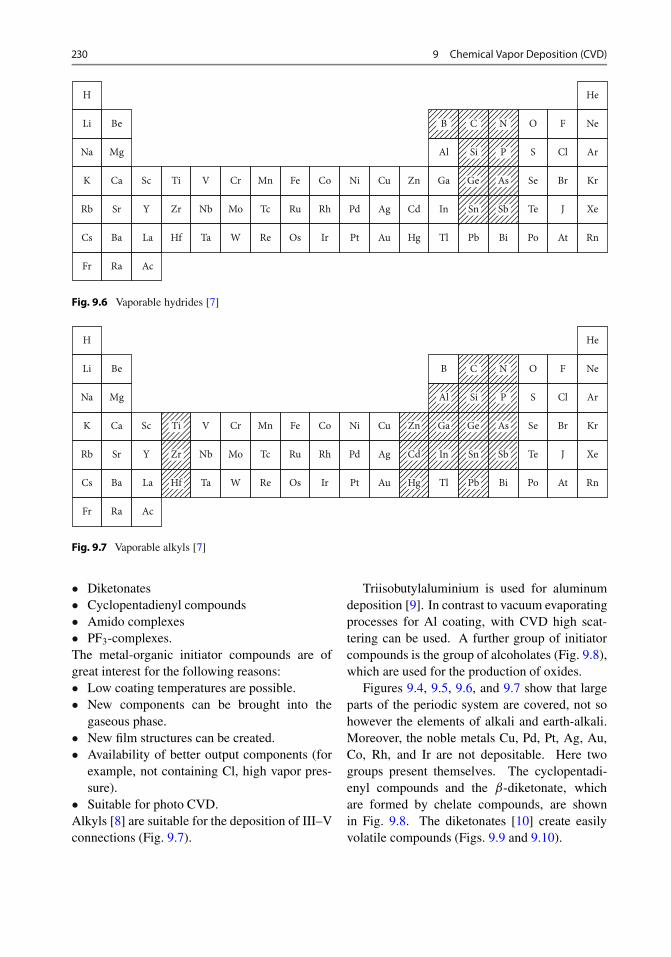
230 9 Chemical Vapor Deposition (CVD)
H
Li
Na Mg
K Ca Sc
YRb Sr
Cs Ba La Ir
Ni
Pd
Pt
Cu
Ag
Au
Zn
Cd
Hg
Ga
In
B
Al
Tl
Ge
Sn
C
Si
Pb
As
Sb
Bi
Se
Te
O
S
Po
Br
J
F
Cl
At
Kr
Xe
Ne
He
Ar
Rn
AcFr Ra
Be
Ti
Zr
Hf
V Cr
Nb
Ta
Mo
W Re Os
Mn
Tc
Fe
Ru
Co
Rh
N
P
Fig. 9.6 Vaporable hydrides [7]
H
Li
Na Mg
K Ca Sc
YRb Sr
Cs Ba La Ir
Ni
Pd
Pt
Cu
Ag
Au
Zn
Cd
Hg
Ga
In
B
Al
Tl
Ge
Sn
C
Si
Pb
As
Sb
Bi
Se
Te
O
S
Po
Br
J
F
Cl
At
Kr
Xe
Ne
He
Ar
Rn
AcFr Ra
Be
Ti
Zr
Hf
V Cr
Nb
Ta
Mo
W Re Os
Mn
Tc
Fe
Ru
Co
Rh
N
P
Fig. 9.7 Vaporable alkyls [7]
� Diketonates� Cyclopentadienyl compounds� Amido complexes� PF3-complexes.The metal-organic initiator compounds are ofgreat interest for the following reasons:� Low coating temperatures are possible.� New components can be brought into the
gaseous phase.� New film structures can be created.� Availability of better output components (for
example, not containing Cl, high vapor pres-sure).
� Suitable for photo CVD.Alkyls [8] are suitable for the deposition of III–Vconnections (Fig. 9.7).
Triisobutylaluminium is used for aluminumdeposition [9]. In contrast to vacuum evaporatingprocesses for Al coating, with CVD high scat-tering can be used. A further group of initiatorcompounds is the group of alcoholates (Fig. 9.8),which are used for the production of oxides.
Figures 9.4, 9.5, 9.6, and 9.7 show that largeparts of the periodic system are covered, not sohowever the elements of alkali and earth-alkali.Moreover, the noble metals Cu, Pd, Pt, Ag, Au,Co, Rh, and Ir are not depositable. Here twogroups present themselves. The cyclopentadi-enyl compounds and the ˇ-diketonate, whichare formed by chelate compounds, are shownin Fig. 9.8. The diketonates [10] create easilyvolatile compounds (Figs. 9.9 and 9.10).

9.2 Physicochemical Bases 231
1.1.1.5.5.5 Hexafluoro-2.4-pentandion1.1.1.5.5.5 Hexafluoroacetylenacetone (hfacac)
2.2-Dimethyl-6.6.7.7.8.8.8-heptafluro-3.5-octandione (hfod)
2.2.6.6-Tetramethyheptan-3.5-dion (tmhd) Dipivaloymethane (dpm)
1.1.1-Trifluro-2.4-pentandium1.1.1-Trifluroacethyaceton (tfacac)
Pentan-2.4-dion acetylacetone (acac)
C
F
F
CF
O
O
O
O
C
H
H
C C
F
H
F C
Me
Me
CMe
O O
C
H
H
C CC
F
F
F
F
C
F
F
F
C
Me
Me
CMe
O O
C
H
H
C MeC
Me
Me
C
H
H
CH
O O
C
H
H
C HC
H
H
C
F
F
CF
O O
C
H
H
C HC
H
H
Fig. 9.8 Chelate compounds for the generation of films with CVD
250
1.9 2.0 2.1 2.21/T
p
mm HgPr Nd Sm Eu
La
Gd Tb Dy Ho Er LuYbTm
2.3 2.410–3K–1
102
10–1
10–2
10
1
°C 225 200 175 150
Fig. 9.9 Vapor pressure of thd (tetramethylheptanedione)complexes [10]
175
2.1 2.2 2.3 2.41/T
ν
p
mm Hg
2.5 2.6 2.7 2.8 2.9 3.110–3K–1
102
1
10–1
10Al(fod)2
Cu(fod)2
Pd(fod)2
Rh(hfa)3
Cu(hfa)2
Cr(hfa)3
Al(hfa)3
Cr(fod)3
Fe(fod)3
Hf(fod)4
Cr(fod)3Al(ac)3
Lu(fod)3
Cr(tfa)3
Al(tfa)3
°C 150 125 100 75 50
Fig. 9.10 Vapor pressure of ˇ-diketonates [10], (Fig. 9.8, hfa D hfacac, fod D hfod, tfa D tfacac, ac D acac)

232 9 Chemical Vapor Deposition (CVD)
Fig. 9.11 Metal halidesand complexes of metalswith organic compoundsfor the production ofmetallic compounds
Connetion class Example Chemical formula Layer materialMetal halogenide Titan tetrachloride Cl
Cl
ClCl
Titan nitride as hardmaterial layer anddiffusion barrier
Metal beta dicetonate Tris (2,26,6-tetramethyl-3,5-heptandionato)
yttrium
Yttrium barium cupratas
superconductor
Metal alcoholates Tantalum (V)-ethylate
Tantalum oxideas dielectric
Metal carbonyles Tungstenhexacarbonyl
Tungsten layers formicroelectronics
Metal alkyles Trichlorethyleneisobutyl aluminum
Aluminum layers asconductive strips
Metalamidocompounds
Tetrakis-(dimethylamido)-
titan
Titaniumnitrideas diffusionbarrier in
microelectronics
Adduct compounds Trimethylaminealan Aluminum layers asconductive strips
Ti
N
N
NN Ti
CH3
C
CH3
C H
H3C C
C
O
O
O
O
O
O
CH3
CH3CH3 C
CC OO
O
O
O
WOC
OC
CO
CO
CO
CO
CH3
CH3
CH3
CH3
Al CH2 C H
CH3
CH3
H3C C
H
H
HAl
C
C
H
H
C H
H
H
An overview of the compound classes for thedeposition of industrially manufactured metalliccompounds is given in Fig. 9.11.
To execute the deposition process the sub-stances must be converted into he gaseous phase.For the execution of the coating an exact dosageof the reaction gases is necessary. To measure gasflows thermal flow meters are usually used. Theprinciple is shown in Fig. 9.12. The gas is ledacross two different pipes; the measurement pipeand the laminar flow element. Depending uponquantity of the gas flow the flow sensor is ad-
justed. The temperatures T1 and T2 are measuredover two temperature sensors, where warmth issupplied to the gas by way of winding heaters be-tween the temperature sensors .
The temperature difference can be determinedvia the Reynolds number
Re D %vd
�; (9.3)
where % is the gas density, � is the viscosity, v isthe medium velocity, and d is the diameters of

9.2 Physicochemical Bases 233
H
S1
T1
T X
X
T2–T1= ΔT
T2
S2
Measurement line
No gas flow With gas flow
Laminar flow element
Fig. 9.12 Principle of a thermal flow meter (S1, S2 tem-perature sensor, H heating)
the capillary and the Prandtl number:
Pr D �%c
�; (9.4)
with the heat conductivity � and the specificheat c at constant pressure, we can determine:
�T D f .Pr;Re/ : (9.5)
The exact process is over the calibration deter-mined. From Eq. (9.5) one can recognize that�T does not depend on the pressure of the flow-ing gas, since the Reynolds number does notdepend on the pressure, but only on the massflow, and the Prandtl number is likewise pressureindependent.
For liquid substances bubblers are used. Withthese the feed gas is directly led through the liq-uid. Figure 9.13 shows such a bubbler. If thedroplet size is too large pulsations occur [11].
The principle of a tube evaporator is shownin Fig. 9.14. A gas is led over the substance,which is evaporated and then enriched in thereaction gas. At higher gas velocities (hexaflu-oroacetylacetone) the mass content is determined
TMG vapor100 cm3H2
H2
PTFE BubblesTMG
Fig. 9.13 Principle of bubblers (example, trimethylgal-lium TMG)
by Cu.hfacac/2 by the evaporation velocity. Atlow velocities the mass content is determined bythe equilibrium pressure.
A possible difficulty with bringing evaporablesubstances into the gaseous phase is the creationof fumigation or aerosol (nebulizer). Figure 9.15shows different stages – depending on the coatingconditions. For a CVD process stage c is optimal.As nebulizer, air nebulizers or ultrasonic nebuliz-ers are used. Ultrasonic nebulizers have a closerparticle spectrum than air nebulizers.
Ultrasonic waves produce capillary oscilla-tions on the liquid surface (Fig. 9.16), with thewavelength [12]:
�K D 2� 3
s
%0!2p; (9.6)
where is the surface stress,%0 the density of the liquid, and!p the angular frequency of the ultrasonic wave.
With increasing sound intensity the amplitudeof the capillary wave increases, which form devi-ates due to increasing nonlinearity from the sinewave. Drops finally develop at high amplitudes;their diameterD lies in the order of magnitude of1=4 of the wavelength. For water, for example,we have ( D 0:073N=m)
D=µm D .=MHz/�2=3 :

234 9 Chemical Vapor Deposition (CVD)
a b 0.7
0.5
0.4
0.3
0.2
0.1
00.01
Heating unit Evaporation surface F
0.02 0.03
T= 112°CT= 103°C
T= 120°C
T= 97°C
0.04
l(STB)p(
cu(h
faca
c)2)
·10–3 g/cm3
I
Fig. 9.14 Mass enrichment of Cu (hfacac) in a tube evaporator a against the gas flow
Nozzle
a b c d
Substrate
Droplet
Aerosol
Vapor
Aerosol
Fig. 9.15 Possibilities of the coating with droplet evapo-ration with different positions of the substrate
Fig. 9.16 Capillary waves with increasing amplitude(from top to bottom) on a liquid surface
9.2.2 Transportation Phase
9.2.2.1 General FunctionThe transportation phase mainly has the func-tion to transport the reactive components to thesurface to be coated. The gaseous phase is fre-quently still modified in order to optimize thecoating conditions. The gaseous phase can bemodified by a gas discharge, Fig. 9.17.
RF-generator
RF-cathode
Vacuum
Gas
Fig. 9.17 Parallel disk reactor

9.2 Physicochemical Bases 235
Photons for surface reactions
Lens
Power measurement
Sealing
Vacuum pump
Window cleaning
Photons forvolume reactions Si-substrate
Heating
Fig. 9.18 Photo CVD reactor with modification of the gaseous phase by a photon beam
Pump
50
260
10
CH4+H2
Pressure gauge
Ø 46Ø 27
Ta-ringØ 18
Si-substrate
Sample holder from quartz
Thermocouple
Ø 6
Ø 10
Fig. 9.19 Hot wire CVD reactor for diamond production
A further alternative for modification is theirradiation with photons (Fig. 9.18). A further al-ternative is shown in Fig. 9.19. The gas streamis preheated to high temperatures by means ofa hot Ta wire and then brought into contact withthe surface to be coated. This method can be
Substrate
Inclined and/or parallelincident flow
ϑ
Perpendicular incident flow(maybe rotary substrate holder)
Fig. 9.20 Holdup flow reactor types
Transient zoneVariation zone
CVD processesPVD processes
ACVD
10310210110–110–3 10–210–4 104
LPCVD
Continuum zone Kn Knudsen zone
Fig. 9.21 Flow zones (ACVD D atmospheric CVD,LPCVD D low pressure CVD)
used for the manufacture of diamond films froma mixture of hydrocarbon and hydrogen [13, 14].To scale up CVD equipment a calculation ofthe flow distribution is necessary. In the fol-lowing, the deposition conditions are analyzed,which describe the coating requirements withinthe diffusion-controlled range in a holdup flowreactor (Fig. 9.20). The characteristic index num-ber for the description of the flow is the Knudsennumber Kn. According to Fig. 9.21 differentcomputer models are applicable, depending onthe zone of the Knudsen number [15].
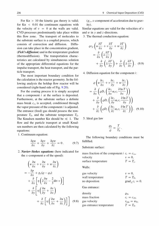
236 9 Chemical Vapor Deposition (CVD)
For Kn > 10 the kinetic gas theory is valid;for Kn < 0:01 the continuum equations withthe velocity of v D 0 at the walls are valid.CVD processes predominantly take place withinthis flow zone. The transport of molecules tothe substrate surface is a coupled process, whichconsists of convection and diffusion. Diffu-sion can take place in the concentration gradient,(Fick’s diffusion) and in the temperature gradient(thermodiffusion). The transportation charac-teristics are calculated by simultaneous solutionof the appropriate differential equations for theimpulse transport, the heat transport, and the par-ticle transport.
The most important boundary condition forthe calculation is the reactor geometry. In the fol-lowing analysis the holdup flow reactor will beconsidered (right-hand side of Fig. 9.20).
For the coating process it is simply acceptedthat a component i at the surface is deposited.Furthermore, at the substrate surface a definitemass break cis is accepted, conditioned throughthe vapor pressure of the component i is adjusted.The entrance (feed) gas should possess the tem-perature T0, and the substrate temperature TS.The Knudsen number Kn should be � 1. Theflow and the particle transport at small Knud-sen numbers are then calculated by the followingequations:1. Continuum equation:
@%u
@xC @%v
@yC @%w
@zD 0 : (9.7)
2. Navier–Stokes equations (here indicated forthe x-component u of the speed):
�u@u
@xC v @u
@yC w@u
@z
�
D �@p@xC gx.% � %0/
C @
@x
��
�2@u
@x� 23
div
�
C @
@y
"
�
�@u
@yC @v
@x
�
C @
@z
��
�@w
@xC @u
@z
�#
(9.8)
(gx , x-component of acceleration due to grav-ity).
Similar equations are valid for the velocities of vand w in y and z-directions.3. The thermal conduction equation:
%cp
�u@T
@xC v @T
@yCw@T
@z
�
D @
@x
��@T
@x
�
C @
@y
��@T
@y
�C @
@z
��@T
@z
�: (9.9)
4. Diffusion equation for the component i :
%
�u@ci
@xC v @ci
@yC w@ci
@z
�
D @
@x
�%Di
�@ci
@x˛ici
@ lnT
@x
��
C @
@y
�%Di
�@ci
@y˛ici
@ lnT
@y
��
C @
@z
�%Di
�@ci
@z˛ici
@ lnT
@z
��: (9.10)
5. Ideal gas law
%0
%D T
T0:
The following boundary conditions must befulfilled.
Substrate surface:
mass fraction of the component i ci D cis,velocity v D 0,surface temperature T D Ts.
Walls:
gas velocity v D 0,wall temperature T D T0,no deposition grad?ci D 0.
Gas entrance:
density %0,mass fraction ci D ci0,gas velocity vein D w0,gas entrance temperature T D T0.

9.2 Physicochemical Bases 237
Gas exit:
dT
dzD dw
dzD dci
dzD 0 :
The mass separation rate is given by the expres-sion
Pmi D %Di.grad?ci C ci˛igrad? lnT / :
For mathematical analysis the gas is regarded asfeed gas (i.e., ci � 1), �; cp , and � and thedensity � does not depend on the reactive com-ponent i . The higher mass fractions �; cp and �are dependent on the component i , and for diffu-sion transport the Stefan–Maxwell equations willbe used [16].
Equations (9.7)–(9.10) are simplified if allsizes related to reference sizes:
x� D x
d; y� D y
d; z� D z
d;
u� D u
w0; v� D v
w0; w� D w
w0;
T � D T
T0; c�
i Dci � C0icis � c0i ; �� D �
�0;
�� D �
�0; c�
p Dcp
cp0; D�
i DDi
D0i
;
%� D %
%0; p� D p
%0v20
;
g�x D
gx
g; g�
y Dgy
g; g�
z Dgz
g;
where the index 0 stands for the gas entrance andthe index s for the values obtained on the sub-strate surface; gx, gy , and gz are the componentsof gravity acceleration.
With these sizes we obtain for the differentialequations:
@%�u�
@x� C@%�v�
@y� C@%�w�
@z� D 0 ; (9.11)
%��u� @u�
@x� C v� @u�
@y� Cw� @u�
@z�
�D �@p
�
@x� Cdggx
�.%� � 1/w20
C �0
%0w0d
@
@x� Œ: : :� : : :
%�c�p
�u� @T �
@x� C v� @T �
@y� Cw� @T �
@z�
�D �0
%0cp0w0d
@
@x�
��� @T �
@x�
�C : : :
%��u� @c�
@x� C v� @c�
@y� Cw� @c�
@z�
�D D0i
dw0
�@�D�
i
@c�
@x�
�C : : :
!
: (9.12)
The boundary conditions are given below.
Gas inlet:
density %� D 1,velocity w� D 1,temperature T � D 1,concentration c�
i D 0.
Substrate surface:v� D 0,T D T �
S ,c�i D 1.
Walls: v� D 0,T � D 1,
grad?c�i D 0.
Gas exit: All gradients in z-directionD 0.
The deposition rate is given through:
Shi D Pmid
.csi � c0i /D0i %0
D %�D�i
grad?c�i
C ˛i�c�i C
c0i
csi � c0i�
grad? lnT �!
;
(9.13)

238 9 Chemical Vapor Deposition (CVD)
where Sh is the Sherwood number. With theSherwood number the mass deposition rate Pmi
can be calculated,
Pmi D .c�si � c�
0i /%0D0i
dShi : (9.14)
We receive the molecular deposition rate underthe condition c � 1:
Ji D .n�si � n�
0i /n0D0i
dShi ; (9.15)
where n�i is the mol fraction of the component i
and n0 the molecular density of the entrance gas.Equations (9.12)–(11.14) depend on the fol-
lowing constants:
dg
w20;
�0
%0cp0dw0;
D0i
dw0;
�0
%0w0d;
T �s ; �
� ; �� ; c�p ; D
�i ;
c0i
csi � c0i ; ˛i :
The first four groups can be transformed into:
dg
w20D 1
Fr
�0
%0cp0dw0D 1
Pr Re
D0i
dw0D 1
SciRe
�0
%0w0dD 1
Re: (9.16)
The Reynolds number Re, the Schmidt num-ber Sci , the Prandtl number Pr, and theFroude number Fr are defined through:
Re D w0d%0
�
Pr D �%0cp
�0
Sci D �0
Di%0
Fr D w20gd
: (9.17)
The Sherwood number depends on these sizes:
Shi D f�x�
s ; y�s ; z
�s ;Re;Sci ;Pr;Fr;
c0
cis � ci0 ;
T �s ; ˛i ; �
�; ��; c�p ;D
�i
�: (9.18)
For the isotherm case the expression reduces to:
Shi D f .x�s ; y
�s ; z
�s ;Re;Sci / : (9.19)
The goal of the mathematical analysis andcalculations is the determination of the Sher-wood number.
In addition the properties of the gases must beknown. With many CVD processes a gas com-ponent (component 2) is available in excess (e.g.,H2, N2, O2). For this gas component �, cp , and �can be used directly.
The binary diffusion coefficients D1 for thediffusion of the component 1 in the gas 2 arealmost never admitted for the reactive gas com-ponents used. These sizes must, therefore, becalculated by means of the kinetic gas theory:
D1 D 0:002628
rT 3.M1 CM2/
2M1M2
p 212˝.1:1/�12
; (9.20)
with D1 in cm2 s�1, p in atm T in K, M1;M2 ing mol�1, 12 in Å.
The reduced impulse functions ˝.1:1/�12 can be
found in tabulated form in [17] and are approxi-mated by analytic expressions in [18].
The impulse functions depend on the quan-tity "12=kT , whereby "12 is the Lennard-Jonesinteraction energy, which in the Lennard-Jonesinteraction potential V12 as well as the Lennard-Jones length 12 determines the dependence onthe distance r :
V12 D 4"1 2�� 12
r
�1 2 �� 12r
�6: (9.21)
Only a few interaction parameters areknown [17], so they must usually be determinedfrom empirical rules. To this end, first the inter-action parameters between the same moleculesi i are estimated, for example, from the boilingtemperatures TS and the molecular volumes VS atthe boiling point .i D 1:2/ [16, 18]:
"i i
kD 1:15 Tsi
i
ÅD 1:18 .Vsi=cm3 mol�1/1=3 : (9.22)

9.2 Physicochemical Bases 239
1
2.0
1.9
1.8
1.7
2.1
1.610–1 10
Reduced temperature T/TC
Redu
ced
expo
nent
υ
Fig. 9.22 Exponent as function of the reduced temper-ature T=Tc
If Vsi is not known it must be numerically cal-culated. By means of arithmetic and geometricalaveraging the interaction energy and interactionlength can be calculated:
12 D 1 C 22
and "12 D p"11"22 : (9.23)
The temperature dependence of the diffusion co-efficients can be determined through
D1 D D10 � T ; (9.24)
where depends on "12=kT .With Eq. (9.20), in Fig. 9.22 the connection
is shown, where is plotted as a function of thetemperatures T=Tc. As a reference temperatureTc D .4=3/."12=k/ has been selected [18].
For the deposition in non-isotherm reactorsthe thermodiffusion can play an important role.The thermodiffusion factor ˛12 depends substan-tially more sensitively on the concrete form of theinteraction potential. Therefore, this value can becalculated only approximately from the kineticgas theory:
˛12 D ��6C �
12 � 56
��2
�12
�S.2/
1C U .2/
U .2/ D 4
15A�12 �
1
12
�12
5B�12 C 1
M2
M1
C .M2 �M1/2
2M1M2
S.2/ D�.M1 CM2/
2M1
�12
�2
� 15
4A�12
�M1 �M2
2M2
� 1
C �12 D ˝.1:2/�
12 =˝.1:1/�
12
A�12 D ˝.2:2/�
12 =˝.2:2/�
12
B�12 D
�5˝
.1:2/�
12 � 4˝.1:3/�
12
�=˝12.1:1/
�
�2
�12D 212 22
˝.2:2/�
12
˝.2:2/�
2
�2M1
M1 CM2
1=2: (9.25)
The reduced collision integrals ˝ are also regis-tered in [18]. The thermal diffusion factors arelocated between 0 and 1.
With the discussed set of equations and thecalculated gas characteristics the flow can be cal-culated (Fig. 9.23); on the basis of these resultswe obtain the Sherwood numbers [16].
The theoretical mathematical analysis showsthe dependence on the Reynolds number and theSchmidt number. The Sherwood number reads:
Sh D ˇpRe3p
Sc : (9.26)
9.2.3 Deposition and Layer Generation
The process steps leading to the development ofthe film are represented in Fig. 9.24.
If all process steps interact the film structure isdeveloped, while for the growth rate usually onlyone of the process steps is important. If only themass transport in the gaseous phase determinesthe deposition, then the considerations discussedin the previous section can be used directly.
If steps 2 to 4 are determinant for the deposi-tion, then the methods of the catalysis for the cal-culations of the deposition are used. An exampleis the SiO2 deposition from SiH4, which can bedescribed by the Langmuir–Hinshelwood mech-anism.
SiH4 and O2 are adsorbed on the surfaceand react with one another to from SiO2. Thedeposition can be reduced with constant SiH4
concentration if too much O2 is in the gaseousphase, since O2 is more strongly adsorbed than

240 9 Chemical Vapor Deposition (CVD)
a b
10 mm 10 mm
0.4
0.06
0.4
0.06
0.6
0.52
–1.8
–1
–2
1
0.2
0.5
Fig. 9.23 Flow lines in a holdup flow reactor (top calculated, bottom made visible by TiO2)
SiH4. The deposition curves for SiO2, whichwere measured in a holdup flow reactor, are rep-resented in Fig. 9.25 [19].
On this basis, a simple model of nucleation isanalyzed and integrated into the growth processof the developing film. During the nucleationthe following are to be differentiated: the ho-mogeneous nucleation within the condensing andcrystallizing phase, for example film and sub-strate from same material, and the heterogeneousnucleation on a substrate surface from differentmaterial. Theories for nucleation are describedin [20–22]. The heterogeneous nucleation is tobe analyzed somewhat more exactly. Accordingto Fig. 9.26, two molecular species A and B areto be adsorbed on the surface and reacted to C.
The collision rate of the molecules on the sur-face is obtained by the Hertz–Knudsen formula
Dilivery transport through gaseous phase
Adsorption/desorption
Surface reaction/surface diffusion
Transformation processes in the film(diffusion, dislocation formation)
Two or three-dimensionalGrowth at stagesand dislocations
Growth of nucleus
Growth of nucleus
Nucleusesgrow together
Fig. 9.24 Fundamental processes of film growth

9.2 Physicochemical Bases 241
XO2
Q
0 0.200.150.100.052.0
1.5
1.0
0.5
0
μm/min
0.25
0 5040302010
668
693
T = 750 K
60
S S
Fig. 9.25 SiO2 deposition rate against the quotient Qfrom the gas flow SiH4 and O2. SiH4 is constant
A B
ϑ γks
γkvγsv
C Nucleus
Fig. 9.26 CVD model including nucleation
.i D A;B/
Ji D pi
.2�mikT /1=2; (9.27)
wherepi is partial pressure of the component i ;T the temperature in the proximity of the surface
(for instance, in the distance of the mean freepath); and
mi the molecular mass.A part of the molecules is chemisorbed, which
is described by the condensation coefficient ˛i :˛i D adsorption rate/impact rate so that the ad-sorption rate is given by: Jiad D ˛Ji .
With metal on metal the condensation co-efficient is ˛i � 1, as long as the substratetemperature is far from the melting point. At theadsorption of external gas molecules, as is usualwith CVD processes, ˛i can deviate stronglyfrom 1.
The adsorption coefficient is then independentof 1; in the simplest case we obtained:
˛ D .1 ��/ ; (9.28)
where � is the total degree of coverage of thesurface.
Here it is accepted that the surface consists ofsimilar types of adsorption locations, which canbe occupied by different molecules:
� DX
i
�i ; �i D i
0; (9.29)
where i is the surface density of the sort of par-ticle I and �i is the degree of coverage of theparticle species i .
The degree of coverage results from the totalbalance. It is accepted that the species of par-ticle C is formed by a binary surface reaction,so that the reaction rate referred to the surface isgiven through:
P C D kAB A B ; (9.30)
where A and B are the surface densities of theparticles A and B. The reaction
C! AC B (9.31)
is given by a similar equation:
P A D P B D kC C : (9.32)
The concentrations A, B, and C, and the de-grees of coverage �A, �B, and �C can now becalculated from the following balances.
Particle species A:
.1 ��/JA D JAds C kAB A B � kC C :
Particle species B:
.1 ��/JB D JBds C kAB A B � kC C :
Particle species C:
kAB A C D kC C : (9.33)
It is accepted that the balances are not affected bythe nucleation.Jids (i D A;B) are the desorption flow den-
sities and are described as equations of the form

242 9 Chemical Vapor Deposition (CVD)
1.0
0.8
0.6
0.4
0.2
00° 30° 60° 90° 120° 150° 180°
ϑ
Fig. 9.27 The correcting function ' against the angle ofcontact ı
Jids D ii exp.�Eids=kT /, (where Eids is theactivation energy of the desorption and i D thefrequency factor).
For the calculation of the nucleuses either themolecular theory by Walton [23] can be used orthe classical nucleation theory, which goes backto Becker and Volmer [24].
According to the classical nucleation theorythe nucleation density is given by
K D C exp
���G
� � '.#/R T
�; (9.34)
where �G� is the free enthalpy for the forma-tion of the critical spherical nucleus, and '.ı/ theformation of calottes at the surface.
The function '.ı/ as given reads,
'.#/ D 14.2C cos#/.1 � cos#/2 ; (9.35)
see Fig. 9.27. The angle of contact ı is describedby the Dupres relation
�sv � �ks D �kv cos# : (9.36)
We can calculate the angle of contact ı from thesurface stresses �sv, �kv, and the interface stress�kv (Fig. 9.28).
For ı D 0 a complete wettability results andfrom Eq. (9.34) it follows that
K D C ; (9.37)
0 500 1000 1500sDeposition time
109
1010
cm–2
2 × 10¹⁰
Nuc
leus
den
sity
Fig. 9.28 Nucleus density; depositing of Au on NaCl
which means that all particles C are nucleuses atthe same time.
For ı D 180ı a homogeneous nucleation takesplace, but no calotte develops on the surface. Thenucleation rate is given by the rate with whichthe critical nucleuses, whose density is given byEq. (9.34), grow further, i.e., becomes supercriti-cal. This rate equals
JK D ! K ; (9.38)
where ! is the frequency, by which particles atthe nucleuses are adsorbed. This frequency canbe estimate by:
! D C � U � ae� EdkT ; (9.39)
whereU is the contour of the nucleuses,a the jump width of the particles,Ed the activation energy for surface diffusion, the pre-exponential factor, and C the molecular surface density in Eq. (9.39)
(particle/unit area).The number of supercritical nucleuses grows
temporally; this was found also experimentally,as shown in Fig. 9.28 [25, 26] for the condensa-tion of Au on NaCl.
The number of nucleuses becomes constantbecause all formed particles bond on the surface

9.2 Physicochemical Bases 243
108
cm–2
6
4
2
107
0 10 20 30 40 50 60 s 70Deposition time
Nuc
leus
den
sity
Fig. 9.29 Nucleus density by the deposition of SiO2
from SiH4 (0.1 Vol.%) and HCl (0.5 Vol.%) in H2 at103 mbar and 1000 ıC
already on the existing nucleuses. This is shownin Fig. 9.28, as well as in Fig. 9.29, where thenumber of nucleuses is illustrated against timewith the generation of Si on SiO2 according tothe CVD process [27].
The nucleuses formed in this way grow to-gether with surface diffusion processes, and thenumber of nucleuses decreases again, as is shownin Fig. 9.31. The time constant for spherical nu-cleuses growing together is given by
tc D 0:56 RT
˝��sDs� a4 ; (9.40)
whereDs is the surface self-diffusion constant,R is the general gas constant,˝ is the molecular volume of the molecules C,� is the surface stress,�s is the thickness of the diffusing film,T is the temperature, andA the surface stress.
The surface diffusion constant Di for anycomponent i is defined through:
Ji D iDi
RTr�i ; (9.41)
wherer is the nabla operator relating to the surface
coordinates,
e
b
a
d
1
10–1
10–2
10–3
10–4
10–5
10–6
10–7
0.7 0.8 0.9 1.0 1.1 1.2 1.3 1.6×10⁻³K–1
1/T
Ds
Fig. 9.30 Changes of the surface diffusion constants ofCu on Cu with simultaneous adsorption of halides for thesystems Cu–Cl (a), Cu–Br (b), Cu–F (c), d and e purecopper
i is the molecular surface density of the diffus-ing particles,
Ji is the molecular molecule flow density at thesurface,
R is the general gas constant,T is the temperature, and�i is the chemical potential at the surface.Di depends on impurities and can, therefore,vary by an order of magnitude of 10, as is shownin Fig. 9.30 with the example of the self-diffusionof Cu on Cu [28].
The temperature dependence of the surfacediffusion constant is described by
Ds D Ds0e�E=RT ; (9.42)
where E is additionally temperature dependent.Equation (9.42) shows that DS increases withtemperature increase.
A correlation between the deposition param-eters and the film structure is difficult, becauseduring the coating the entire film can change. Forexample, a film is to grow epitaxially, which hasa mismatching f of the lattice parameters as, a0of the substrate and the film
f D .as � a0/=a0 :This film grows first, as is shown in Fig. 9.31.Only at a critical thickness ık does the film re-lax partially and it develops dislocations at the

244 9 Chemical Vapor Deposition (CVD)
Fig. 9.31 Epitaxial de-position of films withmismatching for a de-position of thin films, andb partially relaxed films,which develop during thedeposition of thicker films
Undeformed unitcell of the substrate
Generationof dislocations
ElasticallydeformedInterface
Unit cells ofthe substrate
Film
Substrate
a b
boundary surface. This critical thickness lieswithin the range of 50 nm (f D 1%) up to 1 nm(f D 6%). A modeling of the deposition did notsucceed for the nucleation because the number ofparameters in particular is too large.
Numeric calculations, in good agreement withexperimental results, lead qualitatively to the fol-lowing statements:� The nucleus size develops a distribution in the
form of an asymmetrical bell-shaped curve,the maximum shifts with progressive conden-sation to larger nucleuses.
� In the neighborhood of nucleuses the surfaceof adsorbent particles becomes impoverished,and therefore also the probability is small thatin the environment of a nucleus, new nucle-uses will develop.The entire nucleus density increases first, and
afterward it finally reaches a maximum, sincepractically all condensed particles are again at-tached to the existing nucleuses, which is fol-lowed by a decay, because with further growththe nucleuses merge with into a closed film.
9.3 Equipment for CVD Processes
9.3.1 Batch Reactorswith Operating Points Withinthe Kinetically Controlled Range
With CVD, which operates within the kineti-cally controlled range, workpieces can be coatedthree-dimensionally. This is used mainly for thedeposition of hard material films. Figure 9.32
To coatingpieces
Heating
Gas outlet
Gas mixing
Reactorca. 700 ... 1000°C
AlCl3 H2 CO2
TiCl4 H2/N2 CH4
Fig. 9.32 Schema of a batch reactor for coating withAl2O3, TiC, and TiN
Pump
50-200 Wafer
Wafer cartridge
Quartz carrier
Gas inlet
Lower temperatureHigher temperature
Fig. 9.33 Tubular reactor
shows the schema of a batch equipment for de-position hard material films.
In the semiconductor industry, tubular reac-tors (Fig. 9.33), for polycrystalline silicon, SiO2
and Si3N4 from silane coating are used [29].Table 9.2 shows some processes that are accom-plished with tubular reactors.

9.3 Equipment for CVD Processes 245
Table 9.2 CVD processes in tubular reactors
Process Name Reactants Temperature
SiO2 HTO (high temperature oxide) SiH2Cl2 C N2O 850–900 ıC
TEOS (tetra ethyl ortho silicate) Si.OC2H5/4 650–750 ıC
LTO (low temperature oxide) SiH4 C O2 380–430 ıC
(B)PSG (B, P-doped LTO) LTO C PH3 C B2H6 380–430 ıC
Si3N4 Nitrides SiH2Cl2 C NH3 700–800 ıC
SixOyNz Oxynitrides SiH2Cl C NH3 C N2O 700–800 ıC
Poly Si Polysilicon SiH4 580–630 ıC
Doped polysilicon SiH4 C PH3 580–630 ıC
W Tungsten WF6 C H2 250–400 ıC
Al Aluminum Al2.C4H6/3 250–400 ıC
Table 9.3 Films manufactured in holdup flow reactors with atmospheric pressure
SiO2 W O2 C SiH4 ! SiO2 C H4 T D 650–800 K
SiO2 W O3 C TEOS ! SiO2 550–800 K
BSG: O2 C SiH4 C B2H4 ! BSG 650–800 K
PSG: O2 C SiH4 C PH3 C B3H4 ! PSG 650–800 K
BPSG: O2 C SiH4 C PH3 C B2H4 ! BPSG 650–800 K
SnO2 W F W O2 C Sn.CH3/4 C CF3Br ! SnO2 W F 750–800 K
SnO2 W Sb W H2 C CH3OH C SnCl4 C SbCl5 ! SnO2 W Sb 750–800 K
SnO2 W F W SnCl4 C H2O C CH3OH C HF ! SnO2 W F 750–800 K
TiO2 W Ti.OC3H7/4 C H2 ! TiO2 450–650 K
9.3.2 Reactors OperatingWithintheMass-Transport ControlledRange
For Si and/or III–V semiconductors epitaxy bar-rel reactors are used (Fig. 9.34), where the anglebetween the incident flow and the substrate sur-face holder is adjusted so that the coating on thewafer is constant.
A further variant of a holdup flow reactor isshown in Fig. 9.37. A continuous line spray coat-ing system for the production of the films listed inTable 9.3 is illustrated schematically in Fig. 9.38.
A further reactor type, with parallel flow, isthe rotation reactor (Fig. 9.35). The gas mixturesused feed over two gas inlets. The wafer andwafer bracket are being floated with the foarm-ing gas and move in rotation. Figure 9.36 shows
Fig. 9.34 Schema of a barrel reactor
a holdup flow reactor for the deposition of SiO2,phosphorus-glass (PSG), and boron-phosphorus-glass (BPSG).

246 9 Chemical Vapor Deposition (CVD)
Fig. 9.35 Rotation reactor
Substrate
Gas film 2
Gas film 1Rotating diskRotating disk
HeatingWaferholder
WaferA
B
C
Individual coating element 9 individual coating units
Heating
Back side identically to front side
Fig. 9.36 Reactor configurations for the production ofSiO2, PSG, and BPSG
9.4 Plasma-Enhanced ChemicalDeposition from the GaseousPhase (PECVD)
In the case of the plasma-supported chemical de-position from the gaseous phase (PECVD) thenon-thermal, i.e., kinetic electron collision dis-sociation of the background gas or gas mixturebecomes displaced on thermal activation [31].
This is possible where the electron energy typ-ically occurs between Te � 1–5 eV. Since theelectron temperature is very much higher than thesubstrate temperature and the heavy particle tem-perature (due to the thermal uncoupling of theatoms and ions of the electrons), the depositionoccurs during a clearly smaller thermal load ofthe substrate instead as compared with CVD.
SubstrateFlushing gasCarrier band Heating
Gasinjector
N2-protectivegas flow
N2-protectivegas flow
Exha
ust
Exha
ust
Prot
ectiv
e gas
flow
Prot
ectiv
e gas
flow
Fig. 9.37 Spray coating system [30]
Since, however, chemical reactions betweenheavy particles from the gaseous phase are nec-essary with PECVD, the discharge pressurerange with approx. 0.05–10 mbar lies clearlyover the pressure range of the plasma etching(ion-supported etching and reactive ion etching:0.01–0.10 mbar). For this reason, the mean freelength of paths lies within the range of approx-imately 3–300 µm, and is clearly smaller thansputtering or etching.
The plasma density typically lies betweenne D ni D 109 and 5 � 1011 cm�3, and the ion-ization degree " between 10�6 to 10�3.
The surface activation energies for PECVDare usually small. Therefore, the deposition rateis only marginally dependent on the substratetemperature. However, many coating propertiesthat determine the morphology, the composition,

9.4 Plasma-Enhanced Chemical Deposition from the Gaseous Phase (PECVD) 247
Fig. 9.38 Schema ofa continuous line CVDplant; outward pointingarrows show that gas exits
Exhaust
CoolingbandN2
N2 N2HF
N2
N2N2N2N2N2N2N2
Belt dryer
Wafer shuttlefor charging
Band
Heating
Ultrasoniccleaner
Process gases
Wafer shuttlefor discharging
Fig. 9.39 Biodecon re-actor (with quartz disk),ground (with quartz disk)inductive coupled reactor(ICP), antenna and matchbox Cover (with quarz wafer)
Inductively coupled reactorGas shower
Bottom (with quartz wafer)
Antenna +matchbox
the internal stresses, often impact the substratetemperature Tsub very strongly. For this reason,Tsub must be optimized and regulated with re-spect to the required coating properties.
Because of the relatively high pressures and,therefore, small free length of paths and the tem-porally high reaction rates, film uniformity withthe PECVD technique is a critical point. This isintensified by the fact that high sticking proba-bilities with large radical densities are combined,in particular for radicals. Due to this unfavor-able combination of factors the uniformity of thegaseous phase dynamics, i.e., the transport of thegas particles of the inlet must be laid out over the
gas shower up to the pumping system with greataccuracy (Fig. 9.39).
Further, the power density (on the film sur-face) must be controlled and distributed as evenlyas possible. For this reason, the CCP arrange-ment is still important. However, HD plasmasare also used in some cases (Fig. 9.40).
9.4.1 Deposition of Amorphous Silicon(a-Si : H)
The deposition of amorphous silicon is needed(a-Si : H) for many technical applications. Thus,

248 9 Chemical Vapor Deposition (CVD)
RF
RF13.56 MHz
CCP ICP or TCP
Fig. 9.40 Principles of PECVD systems
for the production of thin film transistors sev-eral process steps are needed, in which a-Si : His to be deposited. There are other needs for theproduction of amorphous solar cells a-Si : H coat-ings. Also flat screens and displays are basedon the deposition of a-Si : H films. Contraryto the epitaxial growth, i.e., crystalline siliconwith a density of 2:33 g=cm3, amorphous Si hasa smaller density of approximately 2:2 g=cm3.For the deposition of amorphous silicon, SiH4
(silane) is usually used. With the depositionprocess about 5–20 % H-atoms are built intothe lattice. Thus we obtain amorphous, hydro-gen doped silicon: a-Si : H. The material can bemanufactured favorably and deposited on largesurfaces. As substrate materials glass, metals,polymers, and ceramic(s) are used.
Typical gas mixtures for the production of a-Si : H with PECVD are mixtures of Ar : H2 : SiH4
within the pressure range of 0.25–1.20 mbar. Fordoping typically B2H6 (diborane, p-doping) andPH3 (phosphine, n-doping) are used. In capaci-tive coupled discharges (CCP) at power densitiesbetween 10–100 mW=cm2, we obtain depositionrates of 5–50 nm=min. The substrate temper-atures are typically between 25–400 ıC. Themolecule forms tetrahedrons with the Si atom inthe center. The energy of formation amounts to24.3 kJ=mol. The two radicals SiH2 and SiH3
have a positive electron affinity, i.e., they attractfree electrons and thereby become negativelycharged ions. Binding energies of the radicalsSiH2–H, SiH–H, and Si–H amount to 3.0, 3.4,and 3.0 eV.
Table 9.4 lists some important rate constants.These are usually two-body collisions. As far
as possible, a complete reaction mechanism hasbeen specified by M. Kushner [32]. This modelcontains more than 35 electron collision reac-tions, 90 neutral particle–neutral particle reac-tions, and 80 ions (positive)–neutral particle re-actions, as well as all recombination reactions.
9.4.1.1 Atomic Coating Mechanismin Four Steps
1. Activation and passivation of the (Si) surfaceA passive or passivated surface (coverage p)consists of Si (bulk material) or e.g. H atoms.An active surface (coverage a) from freebonding arms, the so-called dangling bond(Fig. 9.41). Dangling bonds (DBs) are pro-duced by ion bombardment with primarilySiHC
3 , which can also remove H atoms fromthe surface.
2. The SiH2 radicals can be built by collisioninto the solid lattice. This can happen on ac-tive and passive surfaces. In both cases, itconcerns physisorption.
3. The adsorbed SiH3 radicals diffuse along thesurface and contribute to growth only at activeranges. This leads to equalizing of surfaceroughness and contributes thus to growth ofsmooth films of high quality.
4. The adsorbed SiH4 molecule can lose the Hatom at active ranges and thereby passivatethe dangling bond, Fig. 9.42:
θp θa
Si
Si
Si
SiSi
H
Si
Si
SiSi Si
Si
SiSi
Fig. 9.41 Formation of amorphus silicon layers
SiH4 SiH3
Si
Si
SiSi Si
H
Si
SiSi
Fig. 9.42 Saturation of the dangling bonds with hydro-gen

9.4 Plasma-Enhanced Chemical Deposition from the Gaseous Phase (PECVD) 249
Table 9.4 Simplified silane reaction mechanism [32]
Serial no. Reaction Rate constant .cm3=s/
1 e C SiH4 ! SiH3 C H C e 1:5 � 10�8 exp.�10=Te/
2 e C SiH4 ! SiH2 C 2H C e 1:8 � 10�9 exp.�10=Te/
3 e C SiH4 ! SiH�
3 C 2H 1:5 � 10�11 exp.�9=Te/
4 e C SiH4 ! SiH�
2 C H2 9 � 10�12 exp.�9=Te/
5 e C SiH4 ! SiHC
3 C H C 2e 3:3 � 10�9 exp.�12=Te/
6 e C SiH4 ! SiHC
2 C H2 C 2e 4:7 � 10�9 exp.�12=Te/
7 e C SiHC
n ! SiHn�1 C H 2:5 � 10�7T�1=2e
8 SiH4 C H ! SiH3 C H2 2:7 � 10�12
9 SiH4 C SiH2 ! Si2HC
6 1:0 � 10�11
10 Si2HC
6 ! Si2H4 C H2 5:0 � 10C6.1=s/
11 Si2HC
6 C SiH4 ! Si2H6 C SiH4 1:8 � 10�10
12 SiH4 C SiH3 ! Si2H5 C H2 1:8 � 10�15
13 SiH3 C H ! SiH2 C H2 1:0 � 10�10
14 SiH3 C SiH3 ! SiH2 C SiH4 7:0 � 10�12
15 SiH�
m C SiHC
n ! SiHm C SiHn 5:0 � 10�7
Under the condition that the complete surfaceconsists of active and passive or passivated sur-faces, i.e., p C a D 1 is valid.
With 1:
SiHC3 C�p
Kion! �a C YionH.g/ :
where Yion describes the yield of H atoms per in-cident ion.
With 2:
SiH2 C�aK2a!�a ;
SiH2 C�pK2p!�p ;
With 3:
SiH3 C�aK3!�p :
With 4:
SiH4 C�aK4!�p C SiH3.g/ :
With this set of equations the atomic processesare described. However, this represents a sim-plification of the actual conditions. In the next
step, the rate constant (of the particle densitiesinvolved independently) must be determined:
Ki � vBohm
n00
�m3
s
(9.43)
K2a � 1
4
s2av2
n00
K2p � 1
4
s2pv2
n00
(9.44)
K3 � 1
4
Ms3v3
n00
(9.45)
K4 � 1
4
s4v4
n00
; (9.46)
where the sticking coefficient is shown by s2, s3and s4, and M defines the number of danglingbonds that pass the SiH3 radicals on the averageby diffusion before being desorbed (chemisorp-tion).
Under stationary conditions the generationand elimination of dangling bonds are in the equi-librium: where the installation of the SiH2 radi-cals leaves the surface coverage uninfluenced a
d�a
dtŠD 0 D YionKionnion.1 ��a/�K3n3S�a
�K4n4S�a : (9.47)

250 9 Chemical Vapor Deposition (CVD)
The deposition rate is based on the chemical re-lations:
DSi D .K2an2S CK2pn2S CK3n2S�a/n00
nSi;
(9.48)with the solid density nSi.
We summarizeK2aCK2p D K2 and considerthat the SiH4 molecule density is clearly largerthan the ions and the SiH2-radicals densities, i.e.,
K4n4S � YionKionnion CK3n3S ; (9.49)
then with Eq. (9.47) we obtain:
�a D YionKionnion
YionKionnion CK3n3S CK4n4S
� YionKionnion
K4n4S: (9.50)
For typical discharges, nion=n4S � 10�4, Yion �10 and Kion=K4 is valid:
Kion
K4
D vBohm
1=4 � s4v4 DpkTe=mion
1=4pkTg=mion
�sTe
Tg
�r104
102D 10 : (9.51)
Thus we have
�a � 10 � 10104
D 10�2 ; (9.52)
with M � 10 (M is the number of danglingbonds) for SiH3 radicals the effective sticking co-efficient is
s3;eff � s3M�a � 0:1 : (9.53)
For typical deposition conditions the density ofthe SiH2 radical is clearly smaller than those ofthe SiH3 radicals, i.e.,
S3;eff � S3M�a � 0:1 (9.54)
n2S � 10�2n3S ; (9.55)
and thus the third term in Eq. (9.48), which is re-sponsible for good film quality, is approximately
ten time larger than the first two terms, which areresponsible for bad film quality.
Thus with Eqs. (9.48) and (9.50) it becomesclear that a high ion flux is decisive for good filmquality, just like a large n3S=n2S relation as wellas a high surface diffusion of SiH3.
As was already suggested, the mechanismis strongly simplified in the chemical formulas,since, e.g., the first chemical formula is validfor a whole class of ions (and thus of formulas),which can produce dangling bonds by ion bom-bardment of the surface, like, e.g., ArC or SiHC
n
ions. The same is valid also for occupation or freeetching of dangling bonds by hydrogen atoms:
HC a ! p
HC p ! a C H2.g/ :
9.5 Photoinitiated Vapor Deposition
Photoinitiated chemical vapor deposition(piCVD) is an evolutionary CVD technique for de-positing polymeric thin films in one step withoutusing any solvents [33]. The technique requiresno pre or post-treatment and uses a volatile pho-toinitiator to initiate free-radical polymerizationof gaseous monomers under UV irradiation. Gly-cidyl methacrylate (GMA) was used as a testmonomer for its ability to undergo free radicalpolymerization, and 2;20-azobis (2-methylpro-pane) (ABMP) was used as the photoinitiator,as it is known to produce radicals when excitedby photons. GMA and ABMP vapors were fedinto a vacuum chamber in which film growth wasobserved on a substrate exposed to UV irradia-tion. The resulting poly(glycidyl methacrylate)(PGMA) thin films were comprised of linearchains and had high structural resemblance toconventionally polymerized PGMA, as shownby the high solubility in tetrahydrofuran and theinfrared and X-ray photoelectron spectroscopymeasurements. The introduction of ABMP intothe vacuum chamber significantly increasedgrowth rates. The maximum growth rate achievedwas� 140 nm=min, which represents a sevenfold

9.5 Photoinitiated Vapor Deposition 251
enhancement over the case without ABMP. Themolecular weight was found to increase with in-creasing monomer-to-initiator (M=I) feed ratio,and the polydispersity indexes (PDIs) of the sam-ples were between 1.8 and 2.2, which is lowerthan the values obtained in conventional batchpolymerization but in agreement with the theo-retical expressions developed for low-conversionsolution-phase polymerization, which are appli-cable to continuous processes such as piCVD.
Molecular-weight distributions can be nar-rowed by filtering out wavelengths shorter than300 nm, which induce branching and/or cross-linking. The strong dependence of the molecularweight on the M=I ratio, the rate enhancementdue to the use of a radical photoinitiator, thegood agreement between the experimental, andthe theoretical PDIs provide evidence of a free-radical mechanism in piCVD. The clear filmsobtained in this work had number-average molec-ular weights between 12,500 and 97,000 g=mol.The similarities in growth conditions, growthrates, and molecular weights between the initi-ated CVD, a previously reported thermal processable to synthesize a wide range of polymers, andthe piCVD of PGMA suggest that piCVD canalso be used to produce those polymers and po-tentially others whose monomers undergo free-radical mechanisms. This chapter serves as anintroduction to the technique by demonstratingthe ability of piCVD to synthesize high molecularweight PGMA thin films with narrow molecu-lar weight distributions from vapors of GMA andABMP in a single, dry step under UV irradia-tion.
PICVD is based on a new principle of the for-mation of an organometallic vapor phase. A sim-ple idea became the basis for this principle – theentire amount of the precursor mixtures must bestored cool, only their microdoses can be intro-duced into the evaporator. This idea allowed usto elaborate a simple and precise liquid deliverysystem for CVD sources based on the principleused for the control of fuel injection in the latestthermal motors. The injected microdose evap-orates instantaneously (flash evaporation), thus
there is no time for chemical changes of precur-sors.
Volatile organometallic precursors or theirmixture (e.g., Y, Ba, and Cu ˇ-diketonates forYBCO deposition) are dissolved in the appropri-ate organic solvent. The precise microdoses ofsolution are injected into the evaporation zone bymeans of a computer-driven injector, where theyinstantly evaporate. The resulting mixture of sol-vent and precursor vapor is transported by carriergas (Ar, O2) into a high temperature zone wherethe decomposition reaction and film growth oc-cur on a substrate. An injector is a high speedmicro electro valve.
9.5.1 Advantageous Features of PICVD
A microdose (1–10 mg) of solution evaporates in-stantly (flash evaporation) in vacuum .� 5mbar/,so a mixture of precursors is heated for onlya short time, insufficient for chemical change, soinstability of precursors becomes insignificant;the composition of the vapor phase correspondsto the composition of the precursor solution; con-sequently, it is easy to change and reproduce it.
A precise microdosing (within � 3%) of theprecursor mixture, as well as the possibility tochange the injection parameters easily, enablesthe precise control of the vapor pressure, thegrowth rate, and the improvement of the repro-ducibility of film properties.
It is possible to deposit films of various com-position in situ in the same PICVD reactor by asimple change of solution composition and de-position conditions. The use of several injectorsallows production of in situ multi-layered struc-tures.
Another particularity of the process is that itworks “digitally”: the thickness may simply becontrolled by the number of drops injected, whichis very attractive for multi-films. For example, forthe deposition of oxide superlattices, the solutionconcentration, opening time, and droplet size canbe adjusted to obtain a mean thickness increase ateach injection of less than 0.1 nm.

252 9 Chemical Vapor Deposition (CVD)
References
1. Powel CF, Oxley JH, Blocher JM Jr. (eds) (1966) Va-por Depositions. Wiley & Sons, New York
2. Wahl G, Davies PB, Bunshah RF, Joyce BA, BainCD, Wegner G, Remmers M, Walsh FC, Hieber K,Sundgren J-E, Bachmann PK, Miyazawa S, ThelenA, Strathmann H (2000) “Thin Films” Ullmann’sEncyclopedia of Industrial Chemistry. Wiley-VCH,Weinheim
3. Tavares J, Swanson EJ, Coulombe S (2008) PlasmaSynthesis of Coated Metal Nanoparticles with SurfaceProperties Tailored for Dispersion. Plasma Processesand Polymers 5(8):759
4. Chamberlain RR, Skarman JS (1966) Chemical spraydeposition process for inorgqanic films. J Elec-trochem Soc 113(1):88
5. Bloem J (1980) Nucleation and growth of silicon byCVD. J Cryst Groth 50, pp 581/604
6. Simmler W (2005) “Silicon Compounds, Inorganic”,Ullmann’s Encyclopedia of Industrial Chemistry.Wiley-VCH, Weinheim
7. Schleich DM (1989) CVD: a chemical approach toceramic materials. Proc. VIIth Euro CVD Conf. Peri-gan 1989, Ducarroir M, Bernard C, Vandenbulcke L(eds). Publ. by Ed. De Physique, coll de Phys. Additifau Coll C5 suppl. no5 (1989), pp C5-961/C5-979
8. Scalilotti M, Horiuuchi L, Decobert J, Brasil MJ,Cardoso LP, Ossart P, Ganiere JD (1992) Growthand characterization of GaAlAs/GaAs and GaInAs/IPstructures: The effect of a pulse metalorganic flow, JAppl Phys 71:179/186
9. Schmaderer F, Wahl G, Dietrich M, Dustmann CH(1984) Preparation of stabilized superconductingNbCl-y Ny Carbon fibres. In: Mc Robinson D, v dBrekel CHJ, Cullen GW, Blocher JM, Rai-ChoudhuryP (eds) Proc. IX Int. CVD Conf.. ESC, Pennington, pp663–672
10. Sievers RE, Sadlowski JE (1978) Science 201:217
11. Sicre JE, Dubois JT, Eisentraut KJ, Sievers RE (1969)Volatile Lanthanide Chelates. II. Vapor Pressures,Heat of Vaporization and Heats of Sublimation. J AmChem Soc 91:3476/3481
12. Kuttruff H (1988) Physik und Technik des Ultra-schalls. Hirzel Verl., Stuttgart
13. Bachmann PK, Leers D, Lydtin H (1991) Towards ageneral concept of diamond CVD Diamond an relatedMaterials, vol. 1., pp 1–12
14. Isberg J (2004) Single crystal diamond for elec-tronic applications. Diamond and Related Materials13(2):320–324
15. Kennard EH (1938) Kinetic theory of gases. McGraw-Hill, New York
16. Hirschfelder JO, Curtis CF, Bird RB (1954) Molecu-lar Theory of Gases and Liquids. Wiley, New York
17. Reid RC, Prausnitz JM, Sherwood TK (1977) TheProperties of Gases and Liquids. McGraw Hill, NewYork
18. Neufeld PD, Jansen AR, AziZ A (1972) EmiricalEquation to Calculate 16 of Transport Collision In-tegrals˝.1;s/ for the Lennard-Jones (12-6). PotentialTransport. J Chem Phys 57:1100–1102
19. Wahl G (1975) Bocker JM, Hintermann HE, Hall LH(eds) CVD of SiO2 and Boro- and Phospho-Silicateglasses by the reaction of SiH4;B2H6 or PH3 withO2, Proc. Of V Int. Conf. on CVD. ECS, Princeton,pp 391–406
20. Volmer M (1939) Kinetik der Phasenbildung. Verlag.Th. Steinkopff, Dresden, Leipzig
21. Stranski IN (1943/44) 2. Krist. 105:91/123
22. Tammann G (1922) Aggregatzustände. Verlag vonLeopold Voss, Leipzig
23. Walton D (1962) Nucleation of Vapor Deposits. JChemPhys 37:2182–2188
24. Hirth JP, Pound GM (1963) Condensation and evapo-ration. Pergamon Press, Oxford
25. Velfe HD, Stenzel H Krohn M (1982) NucleationData for Gold on Pure NaCl Surfaces, Thin Sol Films98:115/124
26. Jaeger RC (2002) “Film Deposition”. Introduction toMicroelectronic Fabrication, 2nd edn. Prentice Hall,Upper Saddle River
27. Bloem J (1989) Nucleation and growth of silicon byCVD. J Cryst Growth 50:581/604
28. Bonzel HP (1973) Surface Diffusion of Metals Struc-ture and Properties of Metal Surface, vol. 1. MaruzenCompany, Tokyo, pp 248–327
29. Sze SM (2008) Semiconductor devices: physics andtechnology. Wiley-India, ISBN, p 384
30. Watkins Johnson Company, Scotts Valley, CA. Inter-nal Report
31. Ay, Aydinli (2004) Comparative investigation of hy-drogen bonding in silicon based PECVD grown di-electrics for optical waveguides. Optical Materials26(1):33–46
32. Kushner KJ (1988) J Appl Phys 63:2532
33. Felten F, Senateur JP, Weiss F, Madar R, AbrutisA (1995) Deposition of oxides layers by computercontrolled injection-LPCVD. J: Phys: IV F rance5(C5):1079–1086
34. Kelvin C, Gleason KK (2005) Photoinitiated Chemi-cal Vapor Deposition of Polymeric Thin Films Usinga Volatile Photoinitiator, Department of ChemicalEngineering, Massachusetts Institute of Technology,Cambridge, Massachusetts 02139

10Physical Basics of Modern Methods ofSurface and Thin Film AnalysisH. Frey
10.1 Introduction
The characterization of surfaces contains theidentification of the atoms existing at the surface,their classification in crystalline or amorphousstructure, the chemical bonding, and the elec-tronic structure of the surface. By means of thisknowledge we can determine further character-istics, such as dynamic, electrical, thermal, andchemical properties, etc.
With the analysis methods discussed in thischapter, the atoms and molecules at the surfaceare identified due to their mass or their charac-teristic electronic energy states. The method ofthe diffraction of electrons (low energy electrondiffraction LEED, reflection high energy electrondiffraction RHEED) uses the periodic arrange-ment from surface atoms to the determinationof the crystalline structure. The investigation ofthe electron work function also uses a collectivecharacteristic, the potential jump at the surface.
For the investigation of surface structuresnew microscopic methods have been developed,which penetrate into the resolution range ofatomic order of magnitude and also permit time-dependant investigations of dynamic modifica-tions of surface structures or layer growth. Thesurface-analytic methods are based, in princi-ple, on the excitation of the solid surface withphotons, electrons, ions, or neutral particles andreceive information by emitted ions, neutral par-ticles, electrons, and photons or by backscatteredelectrons and ions of the solid surface (Fig. 10.1).
Photons hvElectrons eIons iNeutral particles NElectrical field E
Solid surfaceHeat kT
Photons hvElectrons eIons iNeutral particles N
Fig. 10.1 Possible excitation processes and emissions
Thin film analysis methods have a finite res-olution of depth. The measurable signal comesfrom a certain film depth of the material, andthe appropriate surface composition over thisdepth is averaged. The depth of the analyzedfilm ranges from approximately one atomic layerwith the most surface sensitive methods (e.g.,ion surface scattering – ISS (ion scattering spec-trometry), electron energy loss spectrum EELS)to some 100 nm (e.g., Particde Induced X-RayEmission PIXE).
Methods with monofilm resolution are verymuch suitable for adsorption and desorption in-vestigations. They are also used for the investi-gation of film growth. The question is, whethera thin film monolayer-to-monolayer grows, inthree-dimensional islands or in a combination onthe substrate [1] (Fig. 10.2). In order to be able todifferentiate between these growth forms, atom-layer specific research methods are necessary.The depth of the information also has a connec-tion in relationship with the sample purity and the
253© Springer-Verlag Berlin Heidelberg 2015H. Frey, H. R. Khan, Handbook of Thin-Film Technology, DOI 10.1007/978-3-642-05430-3_10
254 10 Physical Basics of Modern Methods of Surface and Thin Film Analysis
Layer growth
Location growth(Frank-van der Merwe)
Island growth(Volmer-Weber)
Islands on locations(Stranski-Krastanov)
Fig. 10.2 Different modes of film growth caused by thespecific free energy of the surface, that (from top tobottom) decreases due to the occupancy, increases or de-creases only for the first monolayer
vacuum requirements. Methods that are sensitivefor the topmost atomic layer require appropriatesample preparation and ultra high vacuum tech-nology.
Methods, such as (RBS) Rutherford backscat-tering [2–4] with a typical analysis depth of10 nm, can also be operated in the high vacuumrange (10�6 mbar), since the contribution of thetopmost atomic layer to the total signal is suffi-ciently small.
Depth profiles of the sample compound areusually gained by means of gradual abrasion ofthe sample by sputtering. Generally, Ar- ions areused with energies of 1–2 keV. It is to be consid-ered that different materials of compounds havedifferent sputtering rates. The erosion rate canalso change with the depth. The compound ofthe sputtered particles can likewise change [5].Analysis methods that register the particle fluxdropping out from the surface, can, therefore,show different results to methods that observethe respective surface compound in the insidedepth [6]. Figure 10.3 illustrates this.
In the case of a two-component system (A andB) particle conservation in the stationary con-dition results for the concentrations CV in thevolume and C0 at the surface in:
CA0 =C
B0 D
�CA
V =CBV
�.SB=SA/ ;
where S is the concentration-dependant sputter-ing yield.
Fluence
Fluence
C0A
C0B
SB
SA
12
Surfa
ce co
ncen
trat
ion
C 0Sp
utte
ring
yield
S
a
b
Fig. 10.3 Idealized process of sputtering a binary solidsurface with the components A, B, and initial sputteringyields Sb D 2Sa. a Analysis of the surface, b Analysis ofthe flux of sputtered particles
Analysis methods that measure the particleflux from the surface, e.g., SIMS (secondaryion mass spectrometry) [3] or SNMS (secondaryneutral mass spectrometry) [7], register a particlemixture after a transient phase, which corre-sponds to the concentration of the bulk material.
10.2 Ion Spectroscopes
10.2.1 Ion Backscattering
The backscattering of ions is an important toolfor identification of existing atoms at a surfaceand in films near the surface. From the energyof the projectile ion, after the scattering process,the surface atom is identified, and the concen-tration is identified from the scattering intensity(Fig. 10.4).
Chemical bonds or molecules cannot be iden-tified as such. The elastic backscattering of

10.2 Ion Spectroscopes 255
RBS ISS
ERE0
E0=1MeV (4He+→Au)dσ/dΩ≈2·10–6 Å2/sr
(θ=90°)
E0=1keV (4He+→Au)dσ/dΩ≈3·10–2 Å2/sr
(θ=90°)
ε>20 ε<0.3
ER
θ
θ
E0
ε=as E; as=0.47 (Z12/3+Z2
2/3)–1/2ÅM2
(M1+M2)Z1Z2e2
Fig. 10.4 Schematic representation of the ion scatteringwithin different projectile ranges. RBS (high projectileenergy), ISS (low projectile energy). The different differ-ential scattering cross-sections d =d˝ are show by circlesaround the scattering centers. An exact classification pos-
sibility offers the reduced energy " [8]. E is the projectileenergy before the collision, M1,M2 mass numbers of theprojectile and/or target atom, andZ1,Z2 the atomic num-ber of the projectile and/or target
high-energy light ions, usually called Rutherfordbackscattering spectrometry (RBS) [2, 10], hasalso proved to be a very useful tool in the study ofimplantation damage and annealing, the locationof impurity atoms in crystal, and the investigationof surfaces and thin films.
A well-collimated beam of singly ionized 1–3 MeV helium ions or hydrogen ions is used. Thespecimen to be analyzed is placed on a goniome-ter and exposed to the beam in a target chamber ata pressure of 10�6 mbar. The interaction betweenthe projectiles and the surface atoms is deter-mined by the Coulomb repulsion of the atomicnuclei. This method provides absolute quanti-tative results. Information about the specimenis contained in the energy spectrum of the ionsbackscattered through an angle of 140ı. Theseions are detected by a silicon surface barrier de-tector. The signal is amplified and analyzed,stored, displayed, and recorded.
A silicon sample, for example, exposed toa beam of energy E0 gives rise to a spectrumconsisting of a sharp edge at 0:6E0, correspond-ing to helium ions elastically scattered by surface
silicon atoms and deflected into the detector.The sharp edge is followed by a smoothly vary-ing yield at lower energies. Helium ions notscattered at the surface penetrate into the tar-get, losing energy through inelastic collisions andbeing scattered elastically in the bulk. They even-tually leave the target, to be detected after losingmore energy inelastically on the way out. If thestopping power and the geometry of the systemare known, one can convert the energy scale intoa depth scale. If the ion beam is incident in a lowindex direction of a high-quality crystal specimenchanneling develops (see Sect. 6.2.2).
Channeling minimizes collisions of incidentions with target atoms and reduces the observedbackscattered yield for the entire depth in thecrystal. A small surface-damage peak observedonly in the channeled spectrum is due to local-ized surface disorder. Even high-quality crystalsamples show this surface-disorder peak. If thecrystal has been damaged, for example, by ionimplantation, and the displayed atoms occupysites in the channel areas, the channeled ions suf-fer elastic collisions with these atoms, resulting

256 10 Physical Basics of Modern Methods of Surface and Thin Film Analysis
Scat
tere
d io
nsSi
108Ag4He28Si
16O
θ=140°
0 0.2 0.4 0.6E/E0
0.8 1.0
RBS
ISS
Scat
tere
d pa
rtic
les
Fig. 10.5 Schematic representation of the energy spectraof helium ions backscattered under an angle of 140ı ofa Si substrate with Ag, Si, and O on the surface. Up-per spectrum ISS .E0 � 1 keV/, lower spectrum of RBS.E0 � 1MeV/
in a higher scattered yield. The ratio of the yieldin the channeling and nonchanneling directionsis a measure of the quality of single-crystal spec-imens.
RBS, in conjunction with channeling, can alsobe used to determine the concentration and po-sition of impurity atoms in the crystal; the tech-nique has also been applied in a variety of surfacean thin-film problems.
Depth profiles can be analyzed with RBSwithout damaging the surface. The resolution isnot so exact that we can analyze mono-atomicfilms. With low energies around 1 keV the in-teraction is limited to a few atomic layers nearthe surface. This method is designated as ISS orLEIS (low energy ion scattering) [9].
In this energy range the shielding of the nu-clear charge by the electron shell is effective.
The cross-sections are not as exactly calculableas with RBS. The quantitative identification ispossible only with calibration. The neutralizationof the primary ions by the scattering is a furtherproblem. Generally, HeC or NeC ions are used,and the backscattered parts of the ions are ana-lyzed after their energy (Fig. 10.5).
Only ions that are scattered on the top atomiclayer are not neutralized (� 5%) and are therebydetectable. With penetration into deeper atomiclayers less than 10�3 of the backscattered par-ticles are ionized. Recombination is the maincause of the problem of quantification using ISS.At high energies this problem does not arise,since the number of ions is substantially larger.In addition, therefore, the particle used countersneutral particles and ions are countered equally.
The characteristics of both methods deter-mined by the kinetics of the collision are treatedtogether. Both are based on the same physicalprinciples. An ion projectile with the mass M1
has the energy E0 before the collision and af-ter the collision with a surface atom of the massof M2, the energy E1, which can be calculatedfrom energy conservation and momentum con-servation
E1 D E0 K .M2=M1; / ; (10.1)
where the kinematic factor K is
K D
2
664
cos Cr�
M2
M1
�2 � sin2
1C M2
M1
3
775
2
: (10.2)
This means that at a given scattering angle�, de-fined through the analyzing system, the energy isdetermined after collision by the mass M2 of thesurface atom. The measured energy spectrum canbe converted into a mass spectrum. Particularlyfor the scattering angles � D 90ı and � D 180ıwe obtain
K.90ı/ D M2 �M1
M2 CM1
(10.3)
and
K.180ı/ D�M2 �M1
M2 CM1
�2: (10.4)

10.2 Ion Spectroscopes 257
For the scattering angles � > 90ı the ion pro-jectile must have a lower mass than the surfaceatom.
From the analysis of the collision kinetics theresolution of mass M2=�M2 arising in the en-ergy spectrum also results. It is the larger, thecloser the projectile atomic mass and the sampleatomic mass are to each other. For � D 90ı, wehave
M2=�M2 D E1
�E1
2M2=M1
.M2=M1/2 � 1 : (10.5)
By using an energy analyzer with constant rela-tionship E1=�E1 the resolution of energy canonly be improved by a choice of large scatter-ing angles and suitable ion masses. For analyzerswith constant resolution�E one can increase thedistance of appropriate maxima in the spectrumby increasing the primary energy.
The analyzer intensity from scattered ions inthe solid angle �˝ depends on the differentialcross-section d =d˝. For Rutherford Backscat-tering it is accurately defined. In the laboratorysystem we obtain
d
d˝D�Z1Z2e
2
2E0 sin2
�2(10.6)
�h�1 � A�2 � sin2
�1=2 C cos i2
�1 � A�2 � sin2
�1=2 ;
where e is the elementary charge, Z1;Z2 is thenuclear charge numbers of projectile and sampleatom, and A DM2=M1.
For the scattering intensity I from atomicspecies from the areal density N existing on thesurface we obtain with a primary flux I0:
I D N d
d˝�˝I0 : (10.7)
Such measurements of a surface distribution ofthe atomic valuesN gave an accuracy better than10 %, depending on the sample conditions andcan detect less than 1012 atoms=cm2.
With RBS, for scattering from the volume,in addition to the elastic collision the inelasticloss of energy for each paths unit dE=dx must
still be considered. Mainly, dE=dx is gener-ated by interaction with electrons. For a certainatomic mass, one keeps from Eq. (10.1) an edgein the energy spectrum a continuous distributionto smaller energies. These reflect the distribu-tion of the element concerned in the sample depth(Fig. 10.6). The resolution of depth is given bythe collision slowing down power. Typical valuesdE=dx for metals are of an order of magnitude� 800 eV=nm. In the case of a typical resolutionof an energy detector of �E D 6 keV a depthresolution of approximately 7.5 nm results. Thevalues for dE=dx are tabulated in [11].
An example of a film mixture analysis isshown in Fig. 10.6. It shows an RBS spectrum,which was taken up with 2.5 MeV He2C ions ata film of a high temperature superconductor fromYBa2Cu3O7 on a substrate of SrTiO3 [12]. Thetop of the figure shows the spectrum experimen-tally taken up (added noised curve) and a numericfit. The continuous arrows indicate the edgesthat correspond to the scattering of the particularelement at the surface, to Eq. (10.1), and the bro-ken arrows correspond to the scattering of theseelements of the substrate surface. The broken ar-rows contain the additional loss of energy of theions by the passage through the film.
The lower part of the diagram shows the ap-propriate decomposition of the spectrum into thescattering contributions in the different elementsof the film (Ba, Y, Cu). The stoichiometry of thesample can then be calculated from the respectivesignal level Hi of the component i .
One receives approach for conditions of thecomponents i , k,
Ni=Nk D .Hi=Hk/ � .Zk=Zi /2 :ISS is not so exactly calculable and Eq. (10.7)must be extended with the factor P , the so-called ions escape probability. The effectivecross-sections are approximately higher aroundthe factor 104, P is in the order of magnitude10�2, and for light atoms (special for oxygen)the detection limits also lie within the range of1012=cm2;
I D N d
d˝�˝ P I0 : (10.8)

258 10 Physical Basics of Modern Methods of Surface and Thin Film Analysis
Fig. 10.6 RBS spec-trum for the scatteringof 2:5MeV He2C ionsat a superconductingYBa2Cu3O layer. Top:experimental spectrumand numeric simulation(smooth curve). Bottom:decomposition into thescattering fractions of thedifferent components.Continuous arrows re-fer to the surface of thelayer, broken arrows tothe boundary layer to theSrTiO3 substrate
300200
OTi
Sr Cu Y
Ba
HBa
BaY
Cu
SrTiO
100
Energy (Channel number)
Yield
00
20
40
60
0
20
40
60
80100 impulses
channel
With the penetration into the sample volume,generally P degrades on values P 10�4, sothat from the sample volume backscattered ionsplay practically no role. This is valid already fordepths of more than two atomic layers.
10.2.2 Secondary IonMassSpectrometry (SIMS)
In secondary ion mass spectrometry (SIMS) theions sputtered from the surface by a primary ionbeam are monitored in a mass spectrometer. Typ-ically, quadrupole mass spectrometers are usedat resolutions of 1 amu. The imaging of surfaceinhomogeneities can be effected by projectionimages of the secondary ions or by raster scan-ning. Resolutions of the order of 1 µm have beenreported in both cases. The primary beam is
also used to remove surface layers for depth pro-filing, and depth resolutions to 50 Å have beenreported. Figure 10.7 shows the schematic ofa SIMS in which secondary ions are extractedfrom a sample by an electric field and analyzedaccording to their mass-to-charge ratio by a massspectrometer.
For the analysis not only backscattered pri-mary particles can be used, but also ion bombard-ment of the surface replaced secondary particles.When the sample of stripped particles is sput-tered with an ion beam (or also by replacementwith a laser beam), some of the particles leavethe surface positive or negatively ionized (q-foldloaded). These secondary ions can be separatedand detected directly in electromagnetic fields ac-cording to their specific mass M=q (Fig. 10.8).
Also time-of-flight methods are used, wherethe ion characteristic is used for the energy de-
10.2 Ion Spectroscopes 259
Fig. 10.7 Schematic dia-gram of a SIMS system
3 3 2 6 0 1 1
CRT
+15kV
30kV
U2U7
PMT
Sample
10kV
12kV
6As
7kV
U2
U7
termination and for the proof. SIMS is based inprinciple on the sputtering of surface layers. Inaddition, SIMS can be used for the analysis ofthe surface composition. The abrasion of 1010
atoms is sufficient to receive an effectual signal;one speaks of static SIMS [13] (Fig. 10.9).
a
bc
d
e
f
g
h
VS(0–100V)
+29% VS–40%
VS
+VS SEV–2kV
Fig. 10.8 Schematic arrangement of the secondary ion optics of SIMS equipment with energy analyzer and oxygenbeam (the potentials are valid for positive secondary ions). a Sample carousel, b extraction lens, c view lens, d oxygenbeam, e ball condenser, f quadrupole, g pulses, h analog output
Figure 10.9 connects the ablated volume withthe particle number n necessary for the detection(with the statistic error ˙pn), and the diameterof the ion beam used for the sputtering. � is theionization-factor and � the total transmission.Figure 10.9 shows the following correlations. In
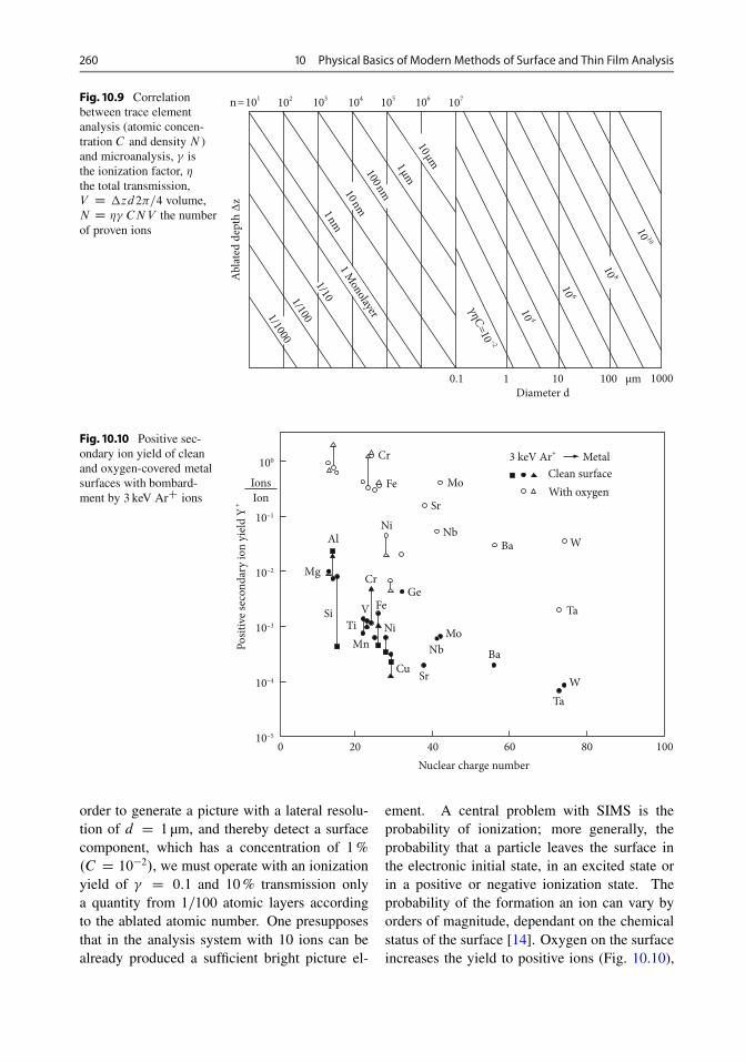
260 10 Physical Basics of Modern Methods of Surface and Thin Film Analysis
Fig. 10.9 Correlationbetween trace elementanalysis (atomic concen-tration C and density N )and microanalysis, � isthe ionization factor, �the total transmission,V D �zd2�=4 volume,N D �� CNV the numberof proven ions
Ablat
ed d
epth
Δz
Diameter d
n=101 102 103 104 105 106 107
0.1 1 10 100 1000μm
10 10
10 6
10 4
γηC=10 –2
1 Monolayer
1/101/1001/1000
10μm1μm100nm10nm1nm
10 8
Fig. 10.10 Positive sec-ondary ion yield of cleanand oxygen-covered metalsurfaces with bombard-ment by 3 keV ArC ions
100
10–1
10–2
10–3
10–4
10–5
IonsIon
Posit
ive s
econ
dary
ion
yiel
d Y
+
0 20 40 60 80 100Nuclear charge number
With oxygenClean surface
WBaNb
Mo
Sr
Cr
Fe
NiAl
GeCr
Fe
NiTiMn
V
Cu Sr
NbMo
Ba
Si
Mg
Ta
TaW
3 keV Ar+ Metal
order to generate a picture with a lateral resolu-tion of d D 1 µm, and thereby detect a surfacecomponent, which has a concentration of 1 %.C D 10�2/, we must operate with an ionizationyield of � D 0:1 and 10 % transmission onlya quantity from 1=100 atomic layers accordingto the ablated atomic number. One presupposesthat in the analysis system with 10 ions can bealready produced a sufficient bright picture el-
ement. A central problem with SIMS is theprobability of ionization; more generally, theprobability that a particle leaves the surface inthe electronic initial state, in an excited state orin a positive or negative ionization state. Theprobability of the formation an ion can vary byorders of magnitude, dependant on the chemicalstatus of the surface [14]. Oxygen on the surfaceincreases the yield to positive ions (Fig. 10.10),

10.2 Ion Spectroscopes 261
Transfer chamber
Sample motion, X
M
M
Stack motion, ZZ
X
Bombardment voltage
Helmholtz coilsCoupling coil
Multiplier
Deflection
Quadrupole
Ion opticsWindow
Valve
Ionsource
Pumping stageSheetSlider
Sample coolingValvePlasma pressure
Sample holder
Sample
Plasma chamber
RF-sheet
Langmuir probes
Stack
Window
Fig. 10.11 Schema of SNMS equipment
and alkali atoms on the surface increase the yieldat negative ions.
In order to achieve as constant and repro-ducible conditions as possible, it is favorable, forpositive SIMS, to saturate the surface with oxy-gen [15]. For the generation of negative ions analkali ion beam [16] is suitable. The uncertaintyin the ion yield is the main problem with quanti-tative SIMS analyses.
The SIMS instrument can operate in threemodes:� An ion microprobe may be used, in which lo-
cal analysis is performed by microfocusing ofthe primary ion beam.
� A true image may be formed by geometricalextraction of the secondary ions and apertur-ing within this image.
� Broad-beam instruments may be used, inwhich analysis over areas greater than 100 µmis performed instead of microanalysis.
SIMS has the following capabilities:� All chemical elements can be observed, in-
cluding hydrogen.� Separate isotopes of an element can be mea-
sured, offering the possibility of determiningself-diffusion coefficients, isotopic dating, andisotopic labeling.
� The area of analysis can be as small as 1 µm indiameter.
� The secondary ions are emitted close to thesurface of the sample.
� The sensitivity of this technique exceeds thatof AES or electron probe microanalysis inmany but not all situations, with detectionlimits in the 10 ppm range under favorableconditions.
� The microanalytical part of this technique canbe used to prepare ion images (ion micro-scope) or ion area scans (ion microprobe),

262 10 Physical Basics of Modern Methods of Surface and Thin Film Analysis
which can give pictorial information about thedistribution of the species of interest.
� Material can be eroded away in a regular andcarefully controlled fashion, and a profile canbe prepared in depth.
10.2.3 Neutral Particle Spectrometry
In order to avoid the difficulties with the yieldof ionized or excited sputtered particles, thepostionization of these particles is a possibil-ity. Methods for this are: the after ionizationby electron collision (secondary neutral massspectroscopy, SNMS) [17, 18], postionization ina plasma by Penning ionization (glow dischargemass spectroscopy, GDMS) [19], excitation bytuned laser radiation (laser induced fluorescence,LIF) [20], and photoionization by lasers [21, 22].
With the direct bombardment method the sam-ple is in a plasma (Fig. 10.11). Between theRF-plasma and the sample a potential differenceis applied for the bombardment (for the excitationof neutral particle emission).
This method can be used for conducting andsemiconducting samples. The ablated area is rel-atively large (of some mm2 up to some cm2) andcan take place at low energies with high lateralhomogeneity.
With isolators instead of a DC voltage poten-tial, a high RF-voltage with suitable frequencyand form is used on the back of the sample.Electrostatic charges are thus avoided and in pe-riodically returning time intervals (f D 10 kHz–1 MHz) the sample is bombarded with plasmaions of constant energy (high frequency method,HFM).
With photoionization three methods can bedifferentiated: resonant multi-photon ionization(REMPI), nonresonant multi-photon ionization(NRMPI), and single-photon ionization (SPI).For most atoms and usual lasers the ionizationenergy is larger than the energy of the photon,therefore a multi-photon process is necessary forthe ionization.
The electrons in the first step are lifted eitherinto a real (lifetime > 10�9 s) or a virtual (life-time � 10�15 s) intermediate state. The typical
Reflector
Transparent degree
Photon path
Primary ion beam
Single lensesLaser beam
Sample
Ion detector
Fig. 10.12 Pattern of the SALI method for the surfaceanalysis by means of a flying time mass spectrometer
power for a pulsed laser is at resonant excitationby 105 W=cm2 and by not resonant excitation109 W=cm2. The non-resonant excitation has theadvantage that one can ionize a broad spectrumof atomic species at the same time. With REMPIone can reach extreme high detection sensitivitiesunder the ppb (parts per billion) range [23].
Figure 10.12 schematically shows the arrange-ment of a surface analysis by means of laserionization (surface analysis by laser ionization,SALI).
The sample atoms sputtered by an ion beamare ionized by the laser beam and flying andthrough a reflecting flying time mass spectrom-eter with a secondary electron multiplier (mi-crochannel plate). The GDMS arrangement isshown in Fig. 10.13 [19].
The sample surface is sputtered by ions fromthe plasma; the ions obtain energy in the cathodefall of approximately 200 eV. Neutral particlesfrom the surface penetrate into the plasma andare ionized by Penning ionization of metastable

10.2 Ion Spectroscopes 263
a
d
Sputtering ofthe sample X
X
X+Arm→X++Ar+e
Ar+ Glow discharge
Penningionization
b
c
X+
≈50mbar Aror
≈200mbar He
p~10–6mbar
Fig. 10.13 Principle and schematic structure of the glowdischarge spectrometry (GMDS). a Hf and cooling water,b grounded screen, c sample holder, d to the mass spec-trometer
He or Ar atoms:
X C Ar� ! XC C ArC e� :
The ionization probability varies around less thanan order of magnitude over the periodic sys-tem; all elements except helium and neon can beproven. The analysis is independent of the elec-trical conductivity of the sample; trace elementanalysis up to less than 1 ppm is easily possible.A lateral resolution is not possible. The sampleis ablated and destroyed by the analysis.
SNMS used a plasma with hot electrodes or anion beam [24]. The method functions in principlewith an ion beam or with ions from the plasma(Fig. 10.14). With SNMS extraordinarily sharpdepth profiles can be obtained, because bombard-ment energies down to 10 eV are possible, and theplasma boundary at the sample surface can be ad-
Fig. 10.14 Schematicarrangement of SNMS.a Sputtering with exter-nal ion gun, b direct ionbombardment from theplasma. a Ion gun, b RF-plasma, d lens system,e quadrupole mass spec-trometer, f Faraday cup,g SEM (secondary electronmultiplier)
a
a b
b
e
f
g
b
ef
g
c
U0+–
c
d
Table 10.1 Absolute ion and photon yield for unsaturatedSi and Ni surfaces
Species Ions or photons/sputtered atom
SiC 1:0 � 10�2
Si2C 1:0 � 10�6
Si I 2882 Å 1:6 � 10�3
Si I 2516 Å 2:2 � 10�4
Si II 3856 Å 1:4 � 10�5
Si II 6347 Å 1:0 � 10�5
NiC 6 � 10�4
Ni I 3415 Å 1:0 � 10�4
Ni I 2325 Å 3:1 � 10�7
justed. Sensitivity is comparable with by SIMSand quantitative analyses are possible.
10.2.4 IPP (Ion-Induced PhotoProduction)
With bombardment of solids, also secondaryparticles in the electronic initial state (neutralparticle and ions) and electronically excited sec-ondary particles are observed [25]. This can beused also for surface analysis. This method iscalled SCANIIF (surface chemical analysis byneutral or ion-induced radiation) [26].
The instrumentation is comparable to SIMS.The mass spectrometer is replaced by equipmentfor optical spectrographic analysis (Fig. 10.15).The spectrographic analysis corresponds tochemical analysis by means of spectroscopy.Table 10.1 shows some estimations to sensitivitycompared with SIMS [27].

264 10 Physical Basics of Modern Methods of Surface and Thin Film Analysis
10.2.5 PIXE (Particle-Induced X-RayEmission)
With PIXE similarly as with electron-induced X-ray spectroscopy (XES), the characteristic X-raysof the sample elements emitted from the surfaceby particle bombardment are measured. For thegeneration ions used (frequently HC or He2C)in the energy range of some 100 keV to someMeV. The advantage of the ions is that the under-ground at bremsstrahlung in the X-ray spectrumis substantially smaller and thus the sensitivitycan be increased. The radiating power of thebremsstrahlung is reversely proportionally to thesquare of the particle mass; around the factor3� 106 a proton thus creates less bremsstrahlungthan an electron of the same energy.
Protons and He ion beams are preferred ifRBS analyses are accomplished at the same time.For the use of PIXE the following is valid: the ef-fective cross-section with proton-induced X-rayemission depend only a little on the atomic num-berZ2 of the sample, which means the sensitivityvaries only within an order of magnitude [28].
The basic effect of PIXE is, as in the caseof AES (Auger electron spectroscopy)and PES(Photoemission spectroscopy), the ionization –prefers in the K-shell – by a high-energy parti-cle with the ionization cross-section 1. Over thefluorescence yield w the effective cross-section x for X-ray emission is connected with the ion-ization cross-section x D .1=w/ 1. w is themean fluorescence yield of the accordingly morehighly lying shell. The activation cross-sectionfor the X-ray emission then results with the ex-perimental photon yield
x D 1
N
dI
dE
dE
dxC 1
N~I ; (10.9)
whereN is the number of the atoms/weight unit,dI=dE the experimental dependence of the in-
tensity from the energy (keV) (photons/par-ticle),
dE=dx the stopping power (keV cm2=g), and~ the self-absorption coefficient of the measured
X-ray in the sample [29].
a
b
c
e
d
Fig. 10.15 Pattern of IPP equipment. a Ion gun, b CObeam, c to the ISS analyzer, d sample, e to the monochro-mator
The data in Fig. 10.15 [30] are average valuesabout experimental data from 81 publications.Q is the averaged normalized effective cross-
sectionQ D 1= theor, where 1 are the averagedexperimental K shell ionization cross-sectionsand theor calculated values [31]. � D 2
p�=Ei
with the velocity relationshipp� D v1=v2k,
where v2k D .Z2 � 0:3/e2=h is the velocityof the electron in the K-shell, and Z2 is theatomic number of the bombarded element. Ei isthe ionization energy of the element concernedin units of the hydrogen ionization energy, i.e.,(Z2 � 0:3/2 Rydberg.
On the basis of the data given in Fig. 10.16 itis possible to indicate analytic formulas for theeffective cross-section with good agreement withexperimental values.
Since the energy range relations for ions insolids are well known [11], with PIXE quan-titative analyses with high sensitivity can beperformed. In practice, relatively simple formu-las can be used for the analysis for thin layers.One determines the effective cross-section asthe sensitivity factor P for the layer (impulsescm3=µCg) with a correction factor F for the

10.3 Electron-Spectroscopic Methods: Auger Electron Spectroscopy and X-Ray Photoelectron Spectroscopy 265
Fig. 10.16 Experimentalaverage values s for theionization effective cross-section of the K-shell forthe elements of the ordinalnumbers 4 � Z2 � 92
with proton bombardmentas function of the scaledsample velocity � in thecomparison to the the-ory (line D 1) and to ananalytic approximationformula (solid line)
1.6
1.4
1.2
1.0
0.8
0.6
0.4
0.2
0–0.8 –0.4 0 0.4 0.8
lg ξ
Q
losses of energy of the protons and the X-ray ab-sorption losses in the layer. Then the linear massdensity of the element i is given by
%i � IiPNPF ; (10.10)
whereIi are the impulses in the X-ray peak of the ele-
ment i , andPN in µC (cm2 s) is the particle current density.
PIXE is non-destructive like RBS and can sup-plement RBS in the case of neighboring masseswith higher resolution.
10.3 Electron-SpectroscopicMethods: Auger ElectronSpectroscopy (AES) and X-RayPhotoelectron Spectroscopy(XPS)
Information carriers in the two most impor-tant thin film analysis methods are electrons(Auger and/or photoelectrons), which leave the
solid body with an element-specific kinetic en-ergy and are analyzed in an electron spectrome-ter. A schematic spectrum of electrons emittedfrom a thin layer under electron bombardment isshown in Fig. 10.17 [32].
Electrons of different origin are observed inthe four energy ranges (I–IV) in Fig. 10.17. Therelative intensity of the various contributions ofthe spectrum depends on the primary energy E0(5–50 keV), the angle of incidence, and the angleof emission. An actual elastic energy spectrumobtained under particular experimental condi-tions may, therefore, differ significantly in shapefrom that of Fig. 10.17. The narrow peak at theincident energyE0 is made up of elastically scat-tered electrons plus diffracted electrons if the thinlayer is crystalline. Energy losses in range I dueto photon excitations (see insert (a) in Fig. 10.17)can be resolved only by the sophisticated energyanalyzers.
In metals and semiconductors most of the en-ergy lost in range II (due to electronic excitationsand ionization losses) is transferred to the con-duction or valence electrons through individual orcollective excitations. In metals, the free electrons

266 10 Physical Basics of Modern Methods of Surface and Thin Film Analysis
a b c d
IV III II I0 50 E0–500 E0–50 E0 (eV)
Phononexcitation
Ionizationand excitation
Atomic excitation mechanisms
Inte
nsity
– ar
bitr
ary
units
Secondary electrons
Elastically scattered electrons True (scattered) secondaries
E0–keV E0–400eV E0–10eV E0–100E0
Phononexcitation
Plasmaexcitation
Augertransitions
Inner shellexcitation
Fig. 10.17 Spectrum of inelastic electrons
can be excited in unison by the incident electronbeam, resulting in a collective or plasma oscil-lation of the valence electrons. Typical energylosses for plasma excitation are around 10–20 eV(see insert (b) in Fig. 10.17). Above 50 eV energylosses (range III), the energy spectrum is shapedby various atomic excitation mechanisms.
The most striking is the appearance of sharpedges corresponding to the excitation of innershell atomic electrons into the vacuum contin-uum (see insert (d) in Fig. 10.17). These edgescorrespond to the energy necessary to ionize theatoms, and the energy loss at which they occuris related to the atomic number. In these pro-cesses a core hole is generated by a primary orsecondary electron and filled by another core orvalence electron. In the Auger process an elec-tron drops down to fill the hole and a secondelectron (Auger electron) is emitted (see insert (c)in Fig. 10.17). In the case of X-ray emission (X-ray fluorescence), instead of the second electrona photon is emitted. These processes (Auger, X-ray emission) are shown in Fig. 10.18.
Finally, range IV (0–50 eV) contains the truesecondary electrons, which are the result of thecascade collision processes of the primary andtarget electrons. The secondary electron dis-tribution (dashed line in Fig. 10.17) shows themost probable energy at 3–5 eV. One cannotfind a clear upper energy limit for secondaryelectrons, but the use of 50 eV is the present con-vention.
For the energy analysis with AES and XPShemisphere or cylinder mirror analyzers are usu-ally used [33]. The mean inelastic free path ofthe electrons in the solid body is limited to afew atom layers and essentially depends on theirkinetic energy. Figure 10.19 shows the meanelectron emission depth of Auger and photoelec-trons as a function of the kinetic energy [31].With AES and XPS fractions of an individualatom layer can be analyzed. By the analysis,therefore, the sample surface may not be con-taminated by rest gases. AES and XPS analysesmust, therefore, be executed under ultra high vac-uum conditions (10�9–10�11 mbar).

10.3 Electron-Spectroscopic Methods: Auger Electron Spectroscopy and X-Ray Photoelectron Spectroscopy 267
ei–
ei–
e–
Valenceshell
Innershells
{
{
ei–
ei–
e–
Valenceshell
Innershells
{
{
X-rayfluorescene
X-rayfluorescene
Auger
a Outer-shell emission
b Inner-shell emission
Auger
e–
e–
hv
Fig. 10.18 Two-step Auger and X-ray fluorescence pro-cess. a Outer shell emission, b inner shell emission
Fig. 10.19 Middle emis-sion depth of Auger andphotoelectrons as a func-tion of their kinetic energy
+ ++ ++
++ +++
++
+
++
Se, AlSe, Au
AuAgAu
SiCa Si
Ni, CdSe
Sr
Ag
Hg
AgMo
BeAg, Au
W Fe
Cu
BeMoW
Ni
Cs CW Be
AgMoCu
++ CuHg Hg
AuAu Au
AuCCu
MoW
WCs
XPS UPS AES+
GeO2
WO3Al2O3
Al2O3
Al2O3
10
1
0.1
nm
Mid
dle e
miss
ion
dept
h λ
10 102 103 104eVEkin
10.3.1 Auger Electron Spectroscopy(AES)
With the Auger process by electron (energy1�10 keV) excitation or photon excitation elec-trons are released from an internal shell of thesample atoms. After this process a hole remainsin this shell, which can be filled by a transi-tion from a higher shell. The energy differencebetween both shells can be emitted as radia-tion (characteristic X-ray) or to a further electronfrom a third shell, which is then emitted in thevacuum. It remains a doubly ionized atom. Thekinetic energy of the emitted Auger electron is infirst approximation
Ee D E1 � E2 � E3 � ˚A :
At homogeneous samples the compound be-tween the concentrations CA of element A andthe appropriate AES signal IA is given by [35]:
CA DIA
I1A
P
j
F AjA �
Ij
I1j
;
where Ij are the intensities of the elements j inthe Auger spectrum of the examined sample and

268 10 Physical Basics of Modern Methods of Surface and Thin Film Analysis
I1j the intensity measured under same experi-
mental conditions at an elementary standard. TheAuger matrix correlation factor F A
jA provides theenergy and matrix dependence of backscatteredprimary electrons, the density of the target atoms,and in general, the matrix-dependant inelasticmean free path � of the Auger electrons [36].
The line intensities of the differentiated spec-trum can be used for the estimation of the surfaceconcentrations (see Fig. 10.20) [37]. There thepeak level in the not differentiatedn.E/-spectrumof the number of exited atoms is proportional, if inthe differentiated spectrum dN=dE, the range be-tween the two peaks, which belong to a line, theconcentration is proportional.
In the energy spectrum the Auger lines ap-pear as weak structures on the underground of theremaining secondary electrons [37, 38]. In theenergy spectrum it is also recognized that withthe Auger electrons also different excitations canbe connected. For example, plasmon excitationsmake a quantitative evaluation more difficult.
The surface sensitivity of AES depends on theemission depth of the electrons in the energy ofthe measured line. Generally, low energy linesfrom atoms near the sample surface are to beexpected. This can be used for simple estima-tions of film thicknesses within the monatomicrange. With adsorbate layers and with the inves-tigation of isolators it should be considered thatthe primary electron beam can also cause disso-ciation and desorption. Figure 10.20b shows anAuger microanalysis of a Raney nickel samplein comparison with an X-ray microanalysis. Themicroanalysis shows that the copper doping is notevenly distributed over the catalyst surface.
Theoretically, the emitted Auger electron fluxIAESi;s can be described as follows:
IAESi;s D I0Tdi;sQi;sNir ; (10.11)
where I0 is the primary current, T the total detec-tion sensitivity, di;s the middle depth from whichthe electrons are emitted, Qi;s the cross-sectionfor the ionization of the K-shell of the atomicspecies i , Ni the concentration (atoms cm�3/ ofthe atoms of the species i , and r the reflectionfactor. Eq. (10.11) is only approximately valid.
An estimation of the activation cross-sections issufficient with Eq. (10.11) to estimate relativeconcentrations at the substrate (constant r).
10.3.2 ESCA (Electron Spectroscopy forChemical Analysis), X-Ray PhotoElectron Spectroscopy (XPS)
A collimated beam of X-rays impinging on a sur-face is more penetrating than an electron beamof the same particle energy and can, therefore,provide more information concerning the consti-tution of the material at greater depths, althoughthe depth is still limited by the range of thephotoelectrons generated. X-rays also producephotoelectrons from the inner shells that carry in-formation concerning the chemical bonding stateof the excited atom. Thus, analysis of the en-ergy distribution of the electrons emitted froma surface bombarded by X-rays is useful forsubsurface chemical analysis. Instruments op-erating on these principles are known as ESCA(electron spectroscopy for chemical analysis) orXPS (X-ray photoelectron spectroscopy) instru-ments [39].
Depending upon the photon energy h onedistinguishes between ultraviolet photo electronspectroscopy (UPS, uses UV-radiation, h withinthe range of 10�40 eV) and X-ray photo electronspectroscopy (XPS, uses X-rays, h D 102–104 eV) [39].
According to Fig. 10.18, the kinetic energy ofthe photoelectrons is:
Ekin D h � EB �˚A ;
where h is Plank’s quantum of action, and ˚A Dwork the analyzer of emission.
At constant photon energy the kinetic energyof the emitted photoelectron depends only on thebinding energy E0 of one atomic level and can,therefore, be used for the identification of the el-ement concerned directly.
XPS supplies information about the bondingstatus of atoms, since with changing distributionof the bonding electrons a shift of the bonding en-ergy in internal electron shells can be observed ofaround several eV [40]. An XPS analysis system

10.3 Electron-Spectroscopic Methods: Auger Electron Spectroscopy and X-Ray Photoelectron Spectroscopy 269
Auge
r int
ensit
y
50 100 150 200 250 300 350 400 450 500 550eV
X10X10
Energy
a
count (lin)
Al Ca
Ni
Ni
1.5 7.5 keV x-ray energy
dN (E)dE
Al S Ca
C
O
Ni Ni Ni
initial state
after sputtering
Al S CaC
O
NiNi
Ni
100 500 900 eVEKin of Augerelectronics
c
d
b
15μm
Fig. 10.20 X-ray microanalysis and Auger microanaly-sis of a Raney Ni sample [38]. b Scanning electronmicroscope picture, c X-ray microanalysis, d Auger mi-
croanalysis, uncleaned (upper spectrum) and cleaned bysputtering (lower spectrum)

270 10 Physical Basics of Modern Methods of Surface and Thin Film Analysis
Fig. 10.21 Schematicrepresentation of XPSequipment
Sphere analyzer
Retardation optic
X-ray-tube
Sphere recipient
Ion source
Sample
To the pumping
consists of a radiation source and an energy an-alyzer with topped electron multiplier. For exci-tation (radiation source) frequently the Mg-K˛1:2
line with 1253.6 eV and a half width of 0.68 eVis used or the Al-K˛1:2 line 1486.6 eV with a halfwidth of 0.83 eV. If the X-ray is by Bragg reflec-tion at a monochromatized crystal, then the halfwidth is reduced to approximately 0.1–0.2 eV;however, with reduction of the intensity [41].
In Fig. 10.21 the schema of XPS equipmentwith an X-ray tube, a sputtering gun for sampleetching and/or for depth profile analysis, and thespherical sector field analyzer is represented [42,43].
10.3.3 UPS (Ultraviolet PhotoelectronSpectroscopy)
UPS is operated particularly with UV line ra-diation by He gas discharge lamps, i.e., with
constant wavelength and/or photon energy. Withsynchrotron radiation it is possible to take up theentire energy sector from UPS to XPS contin-uously. Figure 10.22 schematically shows thedifferences of the diverse photoelectron spec-troscopy methods.
Photon energy in the range between 10 to100 eV is used substantially for the band structureanalysis of solids [44]. Primarily with angle re-solved measurements (ARUPS, angular resolvedultraviolet photoelectron spectroscopy) it is pos-sible to determine both the occupied and theempty bands. Figure 10.23 shows the experimen-tally determined copper band structure [45] com-pared with theoretical results [46]. The theoryis complicated and the calculation is complex.Exact theoretical models exist only for simplemetals and semiconductors.
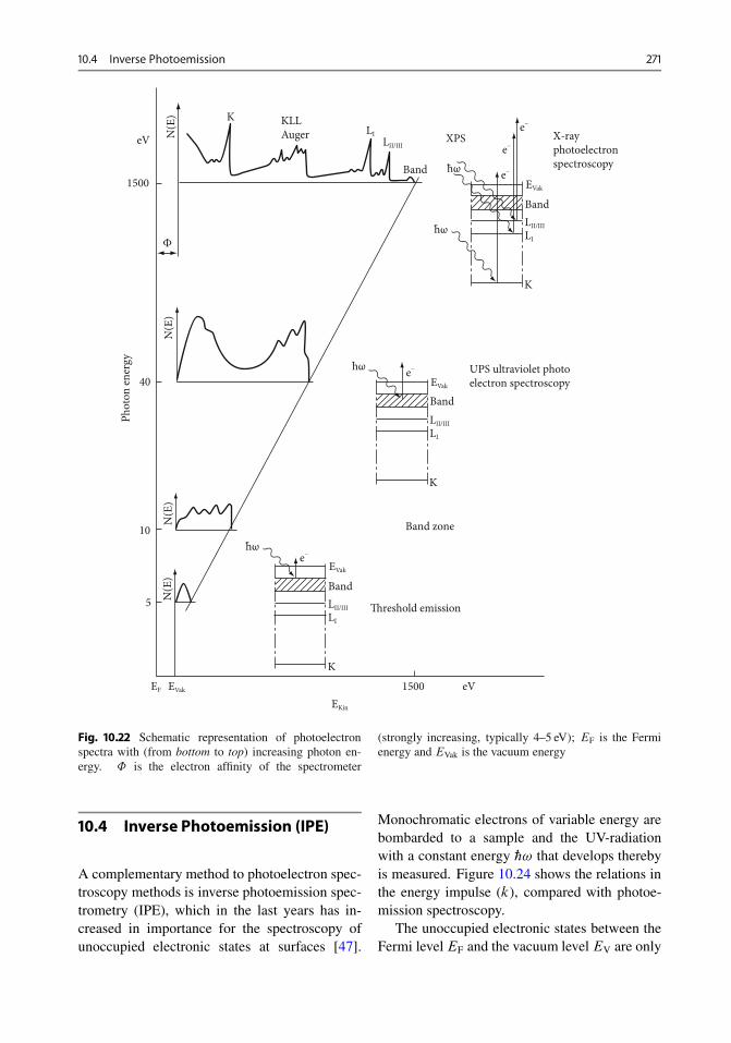
10.4 Inverse Photoemission 271
Band
EVak
LII/IIILI
K
e–hω
BandEVak
LII/IIILI
K
e–hω
Band
EVak
LII/IIILI
K
e–hωe–
e–
hω
K KLLAuger
Band
XPSLII/III
LI
1500
eV
40
10
5
Phot
on en
ergy
N(E
)
Ф
Band zone
Threshold emission
N(E
)N
(E)
N(E
)
EVakEF
EKin
1500 eV
X-rayphotoelectronspectroscopy
UPS ultraviolet photoelectron spectroscopy
Fig. 10.22 Schematic representation of photoelectronspectra with (from bottom to top) increasing photon en-ergy. ˚ is the electron affinity of the spectrometer
(strongly increasing, typically 4–5 eV); EF is the Fermienergy and EVak is the vacuum energy
10.4 Inverse Photoemission (IPE)
A complementary method to photoelectron spec-troscopy methods is inverse photoemission spec-trometry (IPE), which in the last years has in-creased in importance for the spectroscopy ofunoccupied electronic states at surfaces [47].
Monochromatic electrons of variable energy arebombarded to a sample and the UV-radiationwith a constant energy „! that develops therebyis measured. Figure 10.24 shows the relations inthe energy impulse (k), compared with photoe-mission spectroscopy.
The unoccupied electronic states between theFermi levelEF and the vacuum levelEV are only

272 10 Physical Basics of Modern Methods of Surface and Thin Film Analysis
1
2
3
4
5
Ener
gy
eV
2.0 2.5 3.0 3.5 4.0 4.5 5.0Wave vector
K X K Γ
X7+
X7+
X6+
X7+
X6+
Γ8+
Γ7+
Γ8+
+ ++++ +++++++ + ++
+
+ + +
Fig. 10.23 Detail from a band structure identification, if electrons from valence levels are ionized or excited
E
EV
EF
E
EV
EF
Ef
Ei
Ei
Ef
PES BIS/IPE
lf>
li>
hω
li>
lf>
hω
a b
K K
Fig. 10.24 Energy impulse diagram for a photoemission spectroscopy PES and b inverse photoemission IPE

10.6 Diffraction of Slow and Fast Electrons 273
available with the IPE method. The energy statesabove EV are the final state jf i for PES and theinitial states jii for IPE. The IPE method permitsus thus to measure the dispersion curves (en-ergy vs. impulse) of the unoccupied states. Thiswas successfully applied to volume states, sur-face states, and picture potential states. For thinFe layers on Au (100), for example, also quantumwell states were observed [48].
By use of polarized electrons there also existsthe possibility to do a spectroscopy of the elec-tronic states connected with the magnetism (e.g.,spin fragmentation of the d bands at Ni) fromsurfaces and thin layers [49].
10.5 Electron Energy LossSpectroscopy (EELS)
Contrary to the spectroscopy methods describedabove, by which an electron bound in the solidatom is spectroscopically analyzed, EELS (elec-tron energy loss spectroscopy) is a method thatis based on the scattering of electrons. For thescattering process energy and momentum conser-vation are used:
E1 .k1/ D E0 .k0/ � „! ; (10.12)
whereE1 (k1) are the energy and the wave vectorof the scattered electron, E0 .k0/ for the primaryelectron, and „! the oscillation energy or thephonon energy.
For the momentum conservation the compo-nents are to be regarded parallel and perpendicu-larly to the surface, separately; for excitation forphonons, for example, only the parallel compo-nent is substantial:
„k001 D „
�k000 � p00 ˙ G00� ; (10.13)
where p is the phonon impulse and G a latticefactor.
Figure 10.25 shows the EELS spectra of C2H4
on platinum, where independently of the scatter-ing angle different oscillations become excited.EELS show the local character of the availablebonding very exactly.
10.6 Diffraction of Slow and FastElectrons (LEED and RHEED)
The arrangements of the atoms in the surface canbe detected by diffraction methods. Diffractionmethods are analytic methods for the determi-nation of the chemical composition of surfacesand thin films in such a way that they give infor-mation about the arrangement of surface atoms.A condition for this is that the samples whichare to be analyzed possess sufficiently large ar-eas with periodically arranged structures. Wesustain the position of the diffraction maximaby the Ewald sphere construction (Fig. 10.26).In the case of perfect surfaces, points result inthe diffraction pattern, which are frequently de-formed to streaks through defects in the surface.
With RHEED the electrons are scattered overlarger distances along the surface than withLEED. For RHEED lines are characteristicallyin the diffraction pattern (Kikuchi lines [50]),which are explained by the diffraction of inelas-tic scattered electrons at the bulk lattice. Defectsensitivity is also connected with the geometry ofthe experimental structure.
The position of the diffraction maxima isgiven by the Laue conditions
a1�k0 � k0
� D 2 � h ;a2�k0 � k0
� D 2 � k ;a3�k0 � k0
� D 2 � l ; (10.14)
with the wave vectors k0 and k0 of the scatteredand incident waves, the lattice constant a1, a2,a3, and the integer numbers of h; k; andl . WithRHEED the calculation of the intensities is some-what more complicated than with LEED, becauseseveral atomic layers must also be included in thecalculation [51].
RHEED has an experimental advantage com-pared to LEED since for the primary beam andscattered beam, because of the flat incidenceand the small angle on dispersion, only a smallsolid angle in the equipment is coupled by anRHEED arrangement. It is possible to pursue thegrowth process of a film in situ. The RHEEDintensity depends on the quality of the film atthe surface. The diffraction intensity is max-

274 10 Physical Basics of Modern Methods of Surface and Thin Film Analysis
Inte
nsity
0 1000 2000 3000 cm–1
Energy loss
×1
470
×3
790660
1060
980
1430
2930
3000
×5
470
790
660
1060980
1430
560
1230
140
240
50
×5
2920
3000
ФS=0°
ФS=8°
Pt(111)+C2H4
Э=7.4 ·1014cm–2
T=92KE0=2eVθi=θr=72°
Fig. 10.25 EELS spectrum of a Pt (111) surface coveredwith C2H4 Pt (111) in mirror direction (upper spectrum),(s D i � r D 0ı, i D 72ı and with s D 80ı
(lower spectrum). The line identification is indicated withthe lines. The coverage amounts to 7:4 � 1014 cm�2)
imally perfect at the surface and goes througha minimum with maximum disorder, thus e.g.,with an unordered coverage with a half mono-layer. With more unordered multi-layer growthwe achieve an exponentially damped oscillationof the RHEED intensity, as is represented inFig. 10.27 for GaAs. RHEED permits us to ob-serve the growth and the quality of epitaxial filmsin real time.
10.7 ImageMethods
Image spectroscopy methods inform us aboutsurface structures up to atomic dimensions andalso permit dynamic procedures at surfaces witha time resolution from approximately 1 ms to sec-onds to observe.
In the photoemission microscope the localvariations of the photo electron yield (due to adifferent electron affinity e˚/ on the sample sur-face are used during photon irradiation.
In the SPM (scanning photoemission micro-scope) [52] a light beam (h � 6 eV) is focusedon the sample and moved laterally with steppingmotors. In the photo emission electron micro-scope (PEEM) the photoelectrons are imagedby an electrostatic lens system on a fluorescentscreen (Fig. 10.28) [53].
With the LEEM (low energy electron micro-scope) a surface can be imaged both in the lightof directly reflected electrons (local area) and inthe light of a special LEED reflex.
Figure 10.29 shows an LEEM photo of Cuislands of the second monolayer on Mo (110),which recrystallizes spontaneously with this cov-

10.7 Image Methods 275
a
b
d
c
γ
KZ
KY
KX
cγ
33
22
1100
11
22
33
––
––
––
K11––
K11
K00
K0
[110]–
a
b
Fig. 10.26 a Pattern of the Ewald construction. b In thereciprocal area intensity is expected, where the Ewaldsphere with the radius k0 (wave vector of the incident
electrons (19 keV)) reciprocal lattice rods of the zerosLaue zone cuts. That results in the reflexes 1 1, 00 and11. The crystal is thereby in Œ110� – direction orients
Inte
nsity
GaAs (100)
0 5 10 15 20 25sTime
Fig. 10.27 RHEED oscillations by epitaxial growth of GaAs layers on GaAs (100). There are over 20 maxima ob-served, the attenuation refers to unordered multi-position growth
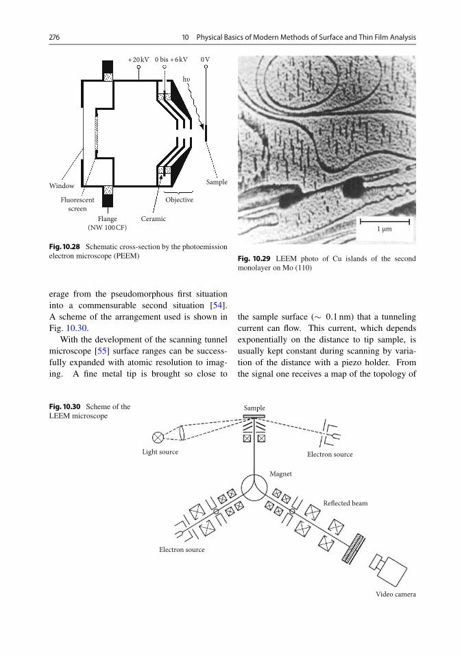
276 10 Physical Basics of Modern Methods of Surface and Thin Film Analysis
+20kV 0 bis +6kV 0V
Sample
Objective
CeramicFlange(NW 100CF)
Fluorescentscreen
Window
hυ
Fig. 10.28 Schematic cross-section by the photoemissionelectron microscope (PEEM)
erage from the pseudomorphous first situationinto a commensurable second situation [54].A scheme of the arrangement used is shown inFig. 10.30.
With the development of the scanning tunnelmicroscope [55] surface ranges can be success-fully expanded with atomic resolution to imag-ing. A fine metal tip is brought so close to
Fig. 10.30 Scheme of theLEEM microscope
Light source
Video camera
Sample
Electron source
Magnet
Reflected beam
Electron source
1 μm
Fig. 10.29 LEEM photo of Cu islands of the secondmonolayer on Mo (110)
the sample surface (� 0:1 nm) that a tunnelingcurrent can flow. This current, which dependsexponentially on the distance to tip sample, isusually kept constant during scanning by varia-tion of the distance with a piezo holder. Fromthe signal one receives a map of the topology of

10.7 References 277
2
1
43
1cm 5 4 4
Fig. 10.30 Scheme raster tunnel microscope. 1 Sampleholder (triple helix), 2 sample, 3 point, 4 Piezo tubes (leg),5 Piezo tubes (feelers)
50.0Å
Fig. 10.31 Scanning tunnel microscopy image(36 nm � 50 nm)
the surface (more exactly, the electronic densityof states).
According to their electronic properties, theobserved corrugation of semiconductor surfaces(stronger localization) is higher than for metalsby about a factor of 5. Figure 10.30 shows thestructure of scanning tunnel microscope equip-ment [56] with the sample approach using a piezocontrolled screw connection of the sample helix.
Figure 10.31 shows the image of a Cu surfacewith atomic resolution faceted by oxygen alloca-tion.
References
1. Bauer E (1984) Z. Krist. 110 (1958), pp. 372, 395.Venables, J.A., G.D.T. Spiller & M. Hanbücken. RepProgr Phys 47:399
2. Chu WK, Mayer JM, Nicolet MA (1978) Backscatter-ing Spectrometry. Academic Press, New York
3. Feuerstein A, Grahmann H, Kalbitzer S, Oetzmann H(1976) In: Meyer O, Linker G, Kappeler F (eds) IonBeam Surface Layer Analysis. Plenum Press, NewYork
4. Davis JA (1978) In: Thomas JF, Cachard A (eds)Material Characterization Using Ion Beams. PlenumPress, London
5. Taglauer E (1982) Appl Surf Sci 13:80
6. Coburn JW, Kay E (1974) Crit Rev Solid State Sci4:63
7. Oechsner H (1995) Secondary Neutral Mass Spec-trometry (SNMS) - Recent Methodical Progressand Applications to Fundamental Studies in Parti-cle/Surface Interaction. Int J Mass Spectrom Ion Pro-cesses 143:271–282
8. Lindhard J, Scharff M, Schiøtt HE (1963) Kgl DanVid Selsk Mat Fys Med 33(14):1
9. Smith DP (1991) J. Appl. Phys. 38 (1967), p. 340.Niehus, H. W. Heiland & E. Taglauer: Surf. SCi. Rep.17 (1993), p. 213, Taglauer. E. In: Ion Spectroscopiesfor Surface Analysis, Ed.: A. W. Czanderna & D.M.Hercules; Plenum Press, New York, p 363
10. Feldman LC (1978) In: Datz S (ed) Applied AtomicCollision Physics, vol 4. Academic Press, New York,p 261
11. Ziegler JF (1977) Helium Stopping Power and Rangesin All Elemental Matter vol. 4. Pergamon, New York
12. Berberich P, Dietsche W, Kinder H, Tate J, ThomsonC, Scherzer B (1988) Proc. Int. Conf. High T Super-cond. Mater Interlaken, CH.
13. Benninghoven A (1973) SurfSci 35:427
14. Wittmaak K (1977) In: Tolk NH, Tully JC, Hei-land W, White CW (eds) Inelastic Particle Ion-SurfaceCollisions. Academic Press, New York, p 153
15. Magee CW, Harrington WL, Honig RF (1978) RevSci Instr 49:477
16. Liebl H, Harrison W (1976) Int J Mass Spectrom, IonPhys 22:237
17. Kato S (ed) (1993) Contributions Third Int. Workshopon Postionization Technique in Surface Analysis LakeKawaguchi, Japan.
18. Schoof, H: Untersuchung an anodischen Tantal- undNioboxidschichten mit AES und SNMS, PhD , Dis-sertation, TU Clausthal 1981
19. Coburn JW, Taglauer E, Kav E (1974) J Appl Phys45:1779

278 10 Physical Basics of Modern Methods of Surface and Thin Film Analysis
20. Schweer B, Bay HL (1982) Appl Phys A 29:53
21. Becker CH (1991) In: Czanderna AW, HerculesDM (eds) Ion Sopectroscopies for Surface Analysis.Plenum Press, New York, p 273
22. Wulff M, Wucher A (1998) In: Gillen G, Lareau R,Bennet J, Stevie F (eds) Quantitation of Single PhotonIonization Laser-SNMS, Secondary Ion Mass Spec-trometry SIMS XI. Whiley, New York, pp 665–666
23. Pellin M, Young CE, Calaway WF, Gruen DM (1984)SurfSci 144:619
24. Hamagaki M, Kato S, Hara T, Hayashi S (1990) Vac-uum 41:1730
25. Goldstein E (1889) Monatsberichte der Köngl PreußAkademie der Wissenschaften zu Berlin 33:108
26. White CW, Simms DL, Tolk NH (1972) Science117:481
27. Tsong IST (1981) In: Taglauer E, Heiland W (eds)Inelastic Particle-Surface Collisions. Springer Seriesin Chemical Physics, vol 17., p 258
28. Pierce TB (1974) In: Kane PF, Larabee GB (eds)Characterization of Solid Surfaces. Plenum Press,New York, p 419
29. Merzbacher E, Lewis HW (1958) In: Flügge S (ed)Handbuch d. Physik, vol 34. Springer-Verl., Berlin
30. Paul H (1984) Nucl Inst Meth B 3:5
31. Brundle CR (1974) The Application of ElectronSpectroscopy to Surface Studies. J Vac Sci Technol11:212–224
32. Hedberg CL (ed) (1995) Handbook of Auger ElectronSpectroscopy, 3rd edn. Physical Electronics, EdenPrairie
33. Holm H, Storp S (1980) Methoden zur Untersuchungvon Oberflächen. In: Ullmans Enzyklopädie der tech-nischen Chemie, vol 5., pp 519–576
34. Brundle CR (1974) The Application of ElectronSpectroscopy to Surface Studies. J Vac Sci Technol11:212–224
35. Seah MP (1983) A Review of Quantitative AugerElectron Spectroscopy. Scanning Electron MicrocII:521–536
36. Seah MP, Dench W (1979) Quantitative ElectronSpectroscopy for Surfaces: A Standard Data Base forElectron Inelastic Mean Free Path in Solids. Surf In-terf Anal 1(1):2–11
37. Ertl G, Küppers J (1985) Low Energy Electrons andSurface Chemistry, 2nd edn. Verlag Chemie, Wein-heim
38. Holm R (1982) Scanning Electron Microscopy III.SEM Inc., Chicago, p 1043
39. Palmberg PW (1976) Quantitative Auger ElectronSpectroscopy Using Elemental Sensivity Factors. JVac Sci Technol 13:214–318
40. Siegbahn K (1970) Electron Spectroscopy for Chemi-cal Analysis (ESCA) Instrumentation. Phil Trans RoySoc Land A 268:33–57
41. Felner-Feldegg H et al (1974) New Developments inESCA-Instrumentation. J Electron Spectrosc Rel Phe-nom 5:643–689
42. Siegbahn K, Nordling C, Johanson G, Hedman J,Heden PF, Hamrin K, Gelius V, Bergmark T, WermeLO, Manne R, Baer Y (1969) ESCA Applied to freemolecules. North-Holland, Amsterdam
43. Cardona M, Ley L (1978) Photoemission in Solidsvol. 1. Springer-Verl., Berlin
44. Spicer WE (1958) Phys Rev 112:225
45. Baalmann A (1984) Dissertation, Universität Os-nabrück
46. Eckhardt H, Fritsche H, Noffke J (1983) J Phys F14:97
47. Dose V (1989) Rendiconti S.I.F. – CVIII 108
48. Himpsel FJ (1991) Phys Rev B 44:5966
49. Donath M, Dose V, Ertl K, Kolac U (1990) Phys RevB 41:5509
50. Kunz C (ed) (1979) Synchrotron Radiation, Tech-niques and Applications Topics in Current Physics.Springer, Berlin
51. Marten H, Meyer-Ehmsen G (1985) Surf Sci 151:570
52. Rotermund HH, Ertl G, Sesselmnn W (1989) Surf Sci217:L 383
53. Rotermund HH, Engel W, Kordesch ME, Ertl G(1990) Nature 343:355
54. Bauer E, Mundschau M, Swiech W, Telieps W (1991)Vacuum 41:5
55. Binning G, Rohre H, Gerber C, Weibel E (1983) PhysRev Lett 50:120
56. Besocke Delta Phi GmbH
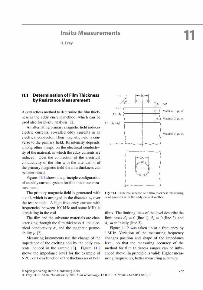
11Insitu MeasurementsH. Frey
11.1 Determination of Film Thicknessby ResistanceMeasurement
A contactless method to determine the film thick-ness is the eddy current method, which can beused also for in-situ analysis [1].
An alternating primary magnetic field induceselectric currents, so-called eddy currents in anelectrical conductor. Their magnetic field is con-verse to the primary field. Its intensity depends,among other things, on the electrical conductiv-ity of the material, in which the eddy currents areinduced. Over the connection of the electricalconductivity of the film with the attenuation ofthe primary magnetic field the film thickness canbe determined.
Figure 11.1 shows the principle configurationof an eddy current system for film thickness mea-surement.
The primary magnetic field is generated witha coil, which is arranged in the distance z0 overthe test sample. A high frequency current withfrequencies between 100 kHz and some MHz iscirculating in the coil.
The film and the substrate materials are char-acterizing through the film thickness d , the elec-trical conductivity , and the magnetic perme-ability � [2].
Measuring instruments use the change of theimpedance of the exciting coil by the eddy cur-rents induced in the sample [3]. Figure 11.2shows the impedance level for the example ofNi/Cu on Fe as function of the thicknesses of both
z r
φ
2r0
2r0
z=0
z=–d1
z=–(d1+d2)
Air
Material 1: μ1, σ1
Material 2: μ2, σ2
Material 3: μ3, σ3
z0
d1
d2
z –∞
Fig. 11.1 Principle scheme of a film thickness measuringconfiguration with the eddy current method
films. The limiting lines of the level describe thelimit cases d1 D 0 (line 1), d2 D 0 (line 2), andd3 D infinitely (line 3).
Figure 11.2 was taken up at a frequency by1 MHz. Variation of the measuring frequencychanges position and shape of the impedancelevel, so that the measuring accuracy of themethod for film thickness ranges can be influ-enced above. In principle is valid: Higher meas-uring frequencies, better measuring accuracy.
279© Springer-Verlag Berlin Heidelberg 2015H. Frey, H. R. Khan, Handbook of Thin-Film Technology, DOI 10.1007/978-3-642-05430-3_11

280 11 Insitu Measurements
11.2 RateMeasurement by ParticleIonization and Excitation
11.2.1 Introduction
For the measurement of the coating rate by ion-ization or excitation of the coating particles dif-ferent methods were developed. By one methodthe coating particles are ionized with low energyelectrons, then the ions passing through a mea-suring cell where the ions integral or specificallymeasured [4]. To it belong the ionization gauge,the periodic beam deflection over a measuringwindow and the mass spectrometer [5]. Insteadof electrons also ions (ion probe) can be used.
Another method uses the emission radiationof excited coating particles induced by electroncollision (EIES, electron impact emission spec-troscopy) [6].
Commercially the method with ion probe,mass spectrometer, and EIES is used.
In Table 11.1 is listed some data for the com-parison of these methods.
11.2.1.1 Ion ProbesFor rate regulation, ion probes can be used in allcases of high vapor ionization [8]. The ionizedfraction of the vapor can be exhausted with a bi-ased probe and used as an analog rate signal.
By electron beam evaporators the possibilitythat the vapor ions can be turned back by themagnetic field in the direction to the cathode canbe used as an ion probe (Fig. 11.3).
If one places a probe sheet near the cathodean ion current can be collected with a suctionvoltage from �50 to about 100 V, which is pro-portional over a wide range to the rate of deposi-tion. By integral measurement also residual gasions are measured. For reproducibility a definedsurface potential of the probe sheet is impor-tant. The method becomes problematic duringthe coating of dielectrics or reactive coating pro-cesses. The probe must shield against an externalcharge carrier, for example, created from a sec-ond electron beam evaporator. The ion probe issuitable in particular for exact regulation of highcoating rates of metals in a non reactive atmo-
Measured pointsCalculated points
1: Cover layer2: Interface layer3: Base material
CopperNickelIron
1.0
0.9
0.8
0.7
0.6
0.5
0.4
0.3
0.2
0.1
00 0.1 0.2 0.3 0.4 0.5 0.6
Fe
Ni
Line 2
Line 3
Line 1
1μm
30μm
3μm
10μm
1μm
3μm
30μm10μm
d1
d2
lm Z
Re Z
Fig. 11.2 Impedance diagram of an eddy current probe atthe system Ni/Cu on Fe. Operating frequency: 1 MHz
a
b
c
d
e
++
+ ++
+–
–
––
–
Fig. 11.3 Functional principle of an ion probe: integratedinto an electron beam evaporator. a Vapor, b ionized va-por, c solenoid coil, d probe disk, e probe voltage
sphere. The advantage is the fast response timeand the small technical expenditure in compari-son to other methods [9].

11.2 Rate Measurement by Particle Ionization and Excitation 281
Table 11.1 Some comparative data for the use of ion probe, mass spectrometer, and EIES
Measurement principle Ion probe Mass spectrometer EIES
Vapor source ES evaporator No restriction No restriction
No pressure dependence Below 10�5 mbar Below 10�5 mbar Below 10�5 mbar
Evaporate from alloyswith 1 source
Integral measurement Selective measurement Selective measurement
Measuring accuracy, rate ˙3% ˙5% ˙2%
Rate zone 0.1–100 nm s�1 10�3–10 nm s�1 0.05–1000 nm�1
Application High ratesmetals
Low rates inultra high vacuum
Evaporation of alloysreactive method
Difficulty Reproducibility e/v overlapby residual gas
Poor photon emitters
Probe surface Disturbance throughES evaporator
Dielectrics Isotopes
Advantage Simply Sensitive Selectivelylong term stabilityuniversal
5
44
3
1 2
Fig. 11.4 Principle of a quadrupole mass spectrometer.1 Filament, 2 electron collector, 3 entrance aperture,4 quadrupole rods, ion collector
11.2.1.2 Mass Spectrometer
11.2.1.2.1 Quadrupole Mass SpectrometerA mass spectrometer separates ions according totheir charge/mass relationship. For rate controlthe quadrupole mass spectrometer [10], devel-oped for the rest gas analysis, is usually used.The quadrupole mass spectrometer does not re-
quire a magnetic field, and in consequence, ismuch less bulky than magnetic types. The instru-ment (Fig. 11.4,) consists of four cylindrical rodsto which a combination of DC and AC potentialsare applied. For a given applied frequency onlyions of a particular value of e=m pass through thespectrometer to the collector.
Ions of different e=m are collected by alteringthe AC frequency. The quadrupole is able to de-tect partial pressure of the order of 10�12 mbar.If the atoms or molecules flow through a win-dow into the ionization measuring cell, a fractionis ionized, about 10�4 by electron bombardment,and measured after selection in the mass filter bya Faraday cage or a photomultiplier. The sensitiv-ity of the quadrupole permits rate measurementsup to 10�3 nm s�1. The measuring cell mustshield carefully against radiance, heat, and scat-tered electrons. The upper limit is given by spacecharge effects in the ionization chamber and liesapproximately at 10 nm s�1.
With the multiplex technique the periodicsampling of several mass values, and multicom-ponent and reactive processes can be controlled.Of special interest is the rate regulation withthe mass spectrometer in the molecular beamepitaxy, because multicomponent films with ex-tremely small rates are deposited.

282 11 Insitu Measurements
11.2.1.2.2 Time-of-Flight Mass SpectrometerThe time-of-flight spectrometer consists ofa pulsed ion source and an ion collector at the op-posite end of an evacuated tube [11]. The ions arecreated by electron bombardment and acceleratedout of source towards the collector by either one,or a series, of electric fields. The short pulse ofions traverses a tube of lengthL; the transit time tof ions of a particular m=e value, with velocity vis decided by
t D L=v : (11.1)
If the potential difference through which the ionsare accelerated is initially V , then
v D .2Ve=m/0:5 (11.2)
and
t D L=.2V /0:5� .m=e/0:5 : (11.3)
At the collector at the far end of the tube, ionswill, therefore, arrive at times decided by m=e.The heavier ions require the longer travel times.Thus each source pulse results in a mass spec-trum that can be analyzed on a laptop. Time-of-flight instruments are usually able to detectpartial pressures of the order of 10�9 mbar.
11.2.1.3 Electron-Induced EmissionSpectrometry (EIES)
Electron-induced emission spectrometry offersinteresting possibilities for rate control. Thevapor flux, which passes through a window inthe measuring head, becomes excited by meansof electron collision with the emission of light(Fig. 11.5).
The photon flux of the excited atoms ormolecules is proportional to the particle flux.The coating rate can be measured with high sen-sitivity .10�2 nm s�1/ and small response time(ms) [7]. A presumption is the selection of inten-sity and perfectly separate spectral lines, whichfor most materials are in the UV (unltraviolet) toVIS (visible) range, for gases also in the IR (in-frared) range (Fig. 11.6).
With unknown emission lines a monochro-mator is used to determine the high intensity
c
d
a
b
Fig. 11.5 Functional principle of an EIES measuringhead. a Photons, b evaporated material, c electrons,d heating spiral
Cu
Cu
Cu
Al
Al
200 300250 350 400 450 500nm
Fig. 11.6 EIES spectrum of an Al/Cu alloy
emission lines. For well-known emission linesedge filter are used. Several components of thecoating material can be detected; with reactiveprocesses a material component with the reac-tive gas can also be detected. The EIES ratemeasurement is relatively insensitive to outsideinfluences.

11.3 Film Thickness and Rate of Deposition Measurements with Quartz Crystal Oscillators 283
11.3 Film Thickness and Rateof Deposition Measurementswith Quartz Crystal Oscillators
11.3.1 Introduction
Quartz crystal oscillators are used in vacuumcoating equipments in the optical and the semi-conductor industry for regulation of the coatingrate and monitoring of the film thickness. Thesedevices operate on the principle that the resonantfrequency of a piezoelectric crystal is changed byadded weight. The frequency change is used tomeasure the coating rate.
11.3.1.1 Frequency Measuring MethodA quartz crystal plate is accurately ground toa thickness l , and metal electrodes evaporate oneach side. When the electrodes are attached toan oscillating circuit, resonance occurs at a fre-quency f , given by
f D T=2l D A=d .Hz/ ; (11.4)
where T is the velocity of sound across thequartz wafer andA is the frequency constant. Forthe usual orientation along which quartz crystalsare cut (called the AT cut) A D 1661 kHz=mm.If an amount of material �m is deposited onthe crystal area F , the effective increase in filmthickness is given by
�l D �m=%F ; (11.5)
where % is the quartz density. Using Eqs. (11.1)and (11.2) we obtain
�f D �f 2�m=A%F or
�m=F D ��f=f 2A% Œg=cm2� : (11.6)
Since the resonance frequency can be monitoredcontinuously, the instrument can be used to mea-sure the rate of deposition.
11.3.1.2 Z -Match®MethodIf the system quartz oscillation and coating areregarded as coupled resonators from two lay-ers, the coupling between the resonator layers
of the sound identifier impedance relationshipz D zF=zQ depends on the deposited film andthe quartz.
The definition equations for the sound identi-fier impedances are given by:
zF D %FF D p%FcF ; zQ D %QQ D p%QcQ ;
(11.7)where Q and cQ are the phase velocity of theshear wave and the shearing stiffness constant re-garding the considered piezoelectrically excitedstanding wave in the thickness direction, and F
and cF the appropriate parameters of the extrinsicfilm. The theory of the coupled resonator fromtwo films gives the following analytic form:
zQ tanQC zF tanF D 0;F D f
fF�; Q D f
fQ� ; (11.8)
By using Eq. (11.7) and the relationship
fF D 1
2lF
rcF
%F; fQ D 1
2lQ
rcQ
%Q(11.9)
inserted into Eq. (11.18), we obtain the relation-ship of the explicit mass loading frequency
mF
mQD � zFfQ
zQ�farctan
�zQ
zFtan
�f
fQ
�: (11.10)
For the most usual coating materials, inTable 11.2 the zF values (bulk values), valid forthe respective solid material, are registered.
A homogeneous mechanical resonator pos-sesses a trivial resonant frequency spectrum.With each harmonic wave frequency an integralmultiple of the primary wave frequency is an in-teger multiple of the primary wave frequency.A resonator from two layers usually possesseszF ¤ zQ, a nontrivial spectrum, with which ineach case the nearby resonant frequencies exhibitunequal distances. For this reason, the resonantfrequencies of a two or multilevel piezoelectricalresonator are called quasi-harmonic.
When we introduce two resonant frequenciesof the spectrum one after another in Eq. (11.9),then we get two linear independent equationsfrom each, which can be solved mathematically.Figure 11.7 shows the block diagram of a two-frequency film thickness measuring instrument.

284 11 Insitu Measurements
Table 11.2 Density %F, specific acoustic impedance zF ofthe coating material and usable coating range maximum,lF for a) frequency measuring method, b) Z-match proce-dure, with acceptance of a tolerated systematic error of
2 %. The used AT cut parameters are: frequency con-stant of A D 1661 kHz=mm, density %Q D 2:649 �103 kg m�3, sound identifier impedance zQ D 8:801 �106 kg m�2 s�1 [12]
Symbol Material Density QF
[103 kg m�2 s]Impedance zF
[106 kg m�2 s]a) Max. IF b) Max. IF
Al Aluminum 2.68 8.42 2.7 45.0
Ag Silver 10.50 18.5 0.5 3.5
AgBr Silver bromide 6.47 7.46 1.1 8.2
AgCl Silver chloride 5.56 6.67 1.3 6.9
As Arsenic 5.73 9.07 1.3 27.5
Au Gold 19.29 23.9 0.3 1.8
B Boron 2.54 22.6 2.2 13.7
Be Beryllium 1.85 16.3 3.0 20.8
C Carbon 2.25 2.70 9.8 4.1
CaF2 Calcium fluoride 3.18 11.3 1.7 16.7
Cd Cadmium 8.64 15.6 0.6 4.7
CdS Cadmium sulfide 4.83 8.63 1.5 43.3
CdTe Cadmium telluride 5.85 8.98 1.3 35.8
Co Cobalt 8.80 26.8 0.6 4.0
Cr Chrome 7.18 28.6 0.8 4.9
Cu Cooper 8.93 20.5 0.6 4.1
Fe Iron 7.86 25.4 0.7 4.4
Ga Gallium 5.85 4.41 1.3 3.1
GaAs Gallium arsenide 5.31 5.54 1.4 4.8
Ge Germanium 5.35 16.9 1.0 7.2
In Indium 7.30 10.5 0.8 8.5
InSb Indium antimonide 5.76 11.4 1.0 9.2
Ir Iridium 22.46 68.6 0.2 1.5
KCl Potassium chloride 1.98 4.29 3.9 9.3
LiF Lithium fluoride 2.64 11.9 2.1 18.8
Mg Magnesium 1.74 5.50 4.2 14.8
MgO Magnesium oxide 3.58 21.5 1.5 10.3
Mn Manganese 7.40 24.3 0.7 4.7
Mo Molybdenum 10.20 34.5 0.5 3.2
NaCl Sodium chloride 2.17 5.61 3.4 12.7
Nb Niobium 8.75 18.0 0.6 4.4
Ni Nickel 8.80 28.3 0.6 4.0
Pb Lead 11.22 7.86 0.7 6.1
PbS Lead sulphide 7.50 15.4 0.7 5.4
Pd Palladium 11.50 22.9 0.5 3.0
Pt Platinum 21.40 37.0 0.3 1.5
Sb Antimony 6.62 11.4 0.8 8.0
Se Selenium 4.82 10.2 1.1 14.1

11.3 Film Thickness and Rate of Deposition Measurements with Quartz Crystal Oscillators 285
Table 11.2 Continued
Symbol Material Density QF
[103 kg m�2 s]Impedance zF
[106 kg m�2 s]a) Max. IF b) Max. IF
Si Silicon 2.32 12.3 2.4 20.6
SiO2 Silicon dioxide 2.20 8.28 3.3 45.0
Sn Tin 7.30 11.2 0.8 7.5
Ta Tantalum 16.60 33.9 0.3 2.1
Te Tellurium 6.25 9.80 0.9 12.6
Ti Titanium 4.50 14.0 1.2 9.4
U Uranium 18.70 39.5 0.3 1.8
V Vanadium 5.80 16.6 0.9 6.6
W Tungsten 19.30 55.2 0.3 1.7
WC Tungsten carbide 13.80 54.9 0.4 2.4
Y Yttrium 4.50 10.8 1.2 13.1
Zn Zinc 7.10 16.7 0.8 5.4
ZnO Zinc oxide 5.61 15.7 1.0 7.2
ZnS Zinc sulphide 40.90 11.3 0.1 1.3
ZnSe Zinc selenide 5.26 12.2 1.0 9.1
Fig. 11.7 Block diagram ofthe two-frequency oscilla-tor
Quartz sensor
Sensor oscillatorcircuit
Frequencydivider Counter
S1
S2
f3
f1
The sensor oscillator circuit contains a band-pass filter in the feedback circuit, which trans-missions ranging from switch S1 can be switchedfrom the primary wave to the third quasi-har-monic wave. At the same time, switching switchS2 to a 1 : 3 frequency divider, the following fre-quency counter for the basic and harmonic waveexcitation can exhibit practically the same fre-quency range.
Equation (11.4) describes the piezoelectricallyactive quartz resonator part by a homogenous ex-pression for a passive foreign film. A more exactanalysis leads to an accurate description for theresonant frequencies of the two-film resonator fora linear model with short circuit electrodes. AnAT cut quartz is used. We then obtain:
K.Q/zQ tanQC zF tanF D 0 (11.11)
K.Q/ D1 � 2k
2
Qtan
Q
2
1 � k2
QtanQ
; (11.12)
mF
mQD � zFfQ
zQ�farctan
�K.Q/
zQ
zFtan
�f
fQ
�;
(11.13)
where k is the natural oscillation of the effec-tive electromagnetic coupling coefficient. In con-trast to Eq. (11.8), Eqs. (11.10) and (11.11), and(11.13) contain a function K.Q/, which takesa value below 1 within the interesting range.K.Q/ zQ can be regarded as the effective spe-cific acoustic impedance of the quartz materialwith short circuit electrodes.

286 11 Insitu Measurements
0.6
0.5
0.4
0.3
0.2
0.1
0 0.1 0.2 0.3 0.4
W Ag
Mg
a
b
Relat
ive m
ass d
ensit
y m
Relative frequency decrease – Δf/f
Fig. 11.8 Dependence of the sensor characteristic of filmthickness measuring quartz on coating material (in the ex-ample W, Ag, Mg) according to the two-layer resonatormodel Eq. (11.13) and/or in good approximation afterEq. (11.10). For the comparison, the a frequency mea-suring method is also shown
11.3.1.3 Characteristic Sensor CurvesThe values (Eqs. (11.13) and (11.10)) are calcu-lated with the help of the sensor functions for fand z calculated m values, which typically dif-fer by only 0.3 % from each other, so that thediagram of the sensor characteristic and/or masssensitivity in the Fig. 11.8 shows both equationswithin the drawing accuracy and the materialdependence of the sensor characteristic. Forpractice, the derivation of the sensor characteris-tic represented in Fig. 11.9 is important, becausethis shows the reciprocal S of the respective sen-sitivity of a measuring quartz as a function ofthe coating material and of the preloading. Fromthe curves it can be recognized that the rate val-ues supplied by unloaded and loaded measuring
4
3
2
1
0 0.1 0.2 0.3 0.4
W Ag
Mg
a
b
Relat
ive m
ass d
ensit
y s
Relative frequency decrease – Δf/f
Fig. 11.9 Dependence of the relative mass sensitivity ofa layer thickness measuring quartz (related to the sensi-tivity of the unloaded quartz) of the preloading and ofthe coating material according to the two-layer resonatormodel. a frequency measuring method, b period timemeasurement method
quartz can differ with measuring instruments thatdo not consider the z value of the coating mate-rial above far more than 100 %.
11.3.1.4 Film RelaxationFor the permanent coating of a measuring quartz,after completion of the coating process, a pro-nounced, exponentially decayed frequency driftof the quartz at a high loading toward to higherfrequency values can be observed [13]. Thisfrequency drift to higher frequency values leadsto lower film thickness measurement values(Fig. 11.10).
Very high preloading of the sensor quartz andvery high coating rates and hard coating materialcan lead to an error in the thickness indication upto 10 %, caused by the film relaxation.

11.4 Optical Measuring Procedures 287
7
6
5
4
3
2
1
μm
0 0.5 1.0 1.5 h 2.0
Laye
r thi
ckne
ss in
dica
tor
RelaxationCoating Time
I Rm
axI F I F+
I R
Fig. 11.10 Schematic representation of film relaxation.lF: : : correct the measured value of the film thickness af-ter relaxation of the film, lg: : : indicate errors in the filmthickness, lRmax : : : max errors due to the relaxation (re-laxation hub, lF C lRmax : : : indication of the film thicknessmeasuring instrument at the end of the coating process)
11.4 Optical Measuring Procedures
11.4.1 Introduction
Optical films are measured about a fractionalamount from a reference wavelength �0 (con-struction wavelength) up to multiples of thiswavelength. The number of films in a film pack-age is between 1 for a single film coating forantireflection and over 100 for an infrared blockfilter system. The reflection curves and the trans-mission curves of the finished film systems mustusually lie within given ranges of tolerance. Thisis possible only if the individual films of the filmsystem are prepared with appropriate accuracy.
The thickness of the films must be measuredduring the coating procedure and be switched offwhen the prescribed film thickness is reached.In the case of optical measuring of the filmthickness the reflection or transmission of a testglass or a substrate is pursued during the coating.Reflection or transmission shows a nonlinear de-pendence on the film thickness. Automation of
the coating process with optical measurement re-quires a complex control system [14].
Advantages of the optical measuring of filmthickness are:� Possibility of direct measurement of the de-
sired properties� Utilization of error compensation effects to in-
crease the reproducibility of the productionprocess
� No limitation on film thickness (important forIR films)
� Large flexibility� Possibility of error diagnostics at the coating
process.In some cases, the optical measurement is
even the only possibility to determine the thick-nesses of applied films. This is, for instance, thecase with coil coating equipment and continuoustunnel equipment.
11.4.2 Systematics of OpticalMeasuring of Film Thickness
Figure 11.11 shows an overview of the opticalmeasuring methods, distinguished according tothe nature of the measurement (monochromaticor spectral) and the position of the measurement(indirectly on test glasses or directly on the sub-strates).
During monochromatic measurement of thecoating process only the changes of the intensityfrom the measuring wavelength are used. Themeasuring wavelength �0 is filtered out of thewideband measuring light by filters or monochro-mators and can be changed between two layers toachieve optimal measuring conditions.
With spectral measurement, with the help ofa spectrometer reflection or transmission will pe-riodically pass through the spectrum within animaginary broad spectral range. The minimumfrequency of these periodic spectral measure-ments depends on the velocity of the coating pro-cess. Figure 11.12 shows the different methods ofindirect and direct measurements and illustratessome typical applications.

288 11 Insitu Measurements
Fig. 11.11 Variationoptions of optical mea-surement
Principle:
Type of measurement:
Location of themeasurement:
Measurements of reflection, transmission or polarization during coating Determination of the film thickness
Monochromatic Spectral
Indirectly on test glasses Directly on substrates
Fig. 11.12 Methods ofthe indirect and directmeasurement
Indirect measurement
- Only 1 test glass- 2 test glasses alternated (A/B method)- Test glass exchange for each 2 layers- Any combination
Direct measurement
- Continuously- Intermittently
Batch equipmentsFlow path equipments
Application in:
Batch equipmentsFlow path equipmentsBelt coating equipments
11.4.2.1 Monochromatic OpticalMeasuring of Film Thickness
Figure 11.13 shows the spectrum of the reflec-tion curve of a high breaking germanium filmwith the refractive index 4.1 on glass measuredwith monochromatic light as a function of thefilm thickness applied, in each case relative tothe measuring wavelength nd/�m (curve a). Thereflection or transmission curve (monitor curve)is periodic and passes through at optical filmthicknesses that correspond to multiples of �m=4
extreme values.Depending on the desired film thickness the
coating process must be terminated when a cer-tain intensity value is reached or when passingthrough one of the extreme values of the monitorcurve. In the first case we speak of level mon-itoring and in the second case of turning valuemonitoring [15].
The attainable switch-off accuracy showsa complicated dependence on the film thickness
100
80
60
40
20
0
Refle
ctio
n
0 0.2 0.4 0.6 0.8 1.0Optical thickness/λ0
%
a
b
Fig. 11.13 Monitor curve of a germanium film on glass(curve a) and associated curve of the switching off er-rors for noise of the reflection measured value of 0.5 %(curve b)
because of the nonlinear process of the monitorcurve. The resulting film thickness or switch-offerrors depend on the quality of the photometer

11.4 Optical Measuring Procedures 289
10
8
6
4
2
0
Laye
r thi
ckne
ss er
ror
0 0.2 0.4 0.6 0.8 1.0Optical thickness/λ0
%
+
++
+
+
+++ +++
+
Theoretical
Experimental
Fig. 11.14 Comparison of the experimentally determinedlayer thickness errors with the theoretical error curve
used, its calibration, and the measuring environ-ment. A deciding influence is due to is due to thelinearity of the photometer and hence the internalnoise of the photometer, as well as the overlaidmechanical oscillations of the coating equipmentto the measured value resolution.
In case of the deposition of a germanium filmwith a measuring wavelength of 2000 nm, thereflection can be calculated a measured value dis-solution of about 0.5 %, shown in Fig. 11.13.With this value the relative film thickness error,represented by curve b, is �d=d . In each case,its identification in the reflection interval of the0.5 % part of the monitor curve on the film thick-ness axle was projected and the appropriate filmthickness interval�d was read off.
The switch-off errors are thus reversely pro-portional to the respective gradient of the monitorcurve. They are the largest in the extreme val-ues of the monitor curve. Curve b in Fig. 11.13considers the possible existing nonlinearity of thephotometer. The theoretical error curve is shownin Fig. 11.14.
The measurements essentially confirm thetheoretical considerations; however, the extremevalues of the practically identified thickness er-rors are compared in relation to the errors withother film thicknesses that were not as highlyreinforced as was theoretically expected. Thisfact can be attributed to the nature of the method
used in this case for the detection of the extremevalues.
For the measurements (Fig. 11.14), the ex-treme values were determined by differentiationof the measuring signal [16], which ensuresa substantially more exact detection of the ex-treme values as for the calculation of switch-offerrors the presupposed comparison of intensityvalues.
11.4.2.1.1 Problems Duringthe Transformation ofMonochromatic Measuringof Film Thickness in Practice
When planning a coating process we can choosebetween different monitor strategies. The cho-sen monitor strategy has an important influenceon the switch-off errors and thus on the repro-ducibility of the entire coating process [15]. Dueto the geometry of the workpiece to be coated itis meaningful to use a deposited test glass to de-termine the film thickness.
For exact film thickness measurements a posi-tive geometrical displacement between test glassfilms and substrate films is favorable. Such a dis-placement exists, if the film thickness on the testglass is larger than that on the substrate. Fre-quently, therefore, the geometrical displacementbetween test glass and substrate is adjusted. Thegeometrical displacement usually depends on thecoating material. The reasons for this are the fol-lowing:� Different evaporation lobe of the different ma-
terials, e.g., for TiO2 and SiO2
� Separate sources of coating for each materialwith different positions in the coating recipi-ent
� Different condensation conditions on testglass and substrate.A further aspect, which must be considered
during the planning of coating equipment is thephysical displacement. A physical displacementbetween test glass and substrate occurs with tem-perature differences and different condensationconditions, which both concern different precoat-ing and coating angles. Consequences of thephysical displacement are refractive index differ-ences between test glass films and substrate films.

290 11 Insitu Measurements
11.4.3 Calculation of Optical FilmSystems
The propagation of a planar, monochromatic andlinear polarized light wave in a medium can bedescribed by the following complex descriptionof the electrical field intensity:
E D E0 exp fiŒ.2�=T /t � .2�N=�/z�g ;(11.14)
where E is the momentary electrical field inten-sity, E0 the amplitude of the electrical field, ithe imaginary unit, T the period duration, � thewavelength of the light wave, z the local coor-dinate, N the complex refractive index of themedium .N D n � ik/, n the refractive indexof the medium and k the extinction coefficient ofthe medium. The electrical field intensity E andthe magnetic field intensity H are coupled overthe so-called optical admittance y with one an-other.
H D yE : (11.15)
The optical admittance of a medium can be cal-culated out the complex refractive index N ofthe medium and the admittance of the vacuumy0.y0 D
p"0=�0/,
y D N y0 : (11.16)
Except for the proportionality factor and dimen-sion factor y0, the optical admittance is equal tothe refractive index of the medium concerned.
If a planar light wave under an angle ˛ strikesany boundary surface between two media withdifferent refractive indices, then the wave ispartly reflected and partly passed. Reflection andtransmission can be calculated from the condi-tion that the components of the electrical andmagnetic field intensity tangential to the bound-ary surface at the passage through the boundarysurface must be constant. These two tangentialcomponents are connected with one another overa modified optical admittance �,
H D �E : (11.17)
With the angular incidence of light on the bound-ary surface it must be differentiated between the
optical admittance for parallel �k and perpendic-ularly �? polarized light,
�k D y= cos.˛/
�? D y= cos.˛/ : (11.18)
For the reflectance at this boundary surface weobtain:
R Dˇˇˇˇ�0 � �1�0 C �1
ˇˇˇˇ
2
: (11.19)
Here, the indices denote the incidence medium 0and the emergence medium 1. Inserting inEq. (11.19) the relations of Eq. (11.18), we ob-tain the well-known Fresnel equations for thereflection of a plane wave at the boundary sur-face of two media. If such a polarized, pla-nar, monochromatic light wave transits a coatedmedium, then it is reflected several times backand forth at the boundary surfaces.
The overlaying partial waves interfere witheach other and generate electric and magneticfieldes. The field components tangential to theboundary surfaces of the coated media E andH are connected with one another at a positionwith the tangential field components E 0 and H 0at another position by the following relationshipmatrices:
�E
H
D�M11 M12
M21 M22
�E 0H 0
: (11.20)
In particular, this is valid also for the connec-tion of the electromagnetic fields of two adjacentboundary surfaces a and b, since the tangentialcomponents of the field force at these boundarysurfaces are continuous.
For the matrix we then obtain:
�Ea
Ha
D�
cos.ı/ .i=�/ sin.ı/i � sin.ı/ cos.ı/
�Eb
Hb
:
(11.21)The components of the matrix depend only on theproperties of the film at both boundary surfaces.This is, therefore also called the characteristicmatrix of a film.
The optical admittance � of the coating mate-rial can be calculated from the relations (11.18).

11.4 Optical Measuring Procedures 291
Thereby it must be differentiated between paral-lel and perpendicularly to the plane of incidenceof the polarized light.
The phase factor ı calculates itself afterEq. (11.22):
ı D 2�Nd cos.˛/=� ; (11.22)
whereN is the complex refractive index of the film,d the geometrical thickness of the film and˛ the propagation angle of the light in the film
relative to the axis of propagation.In the case of a film system with several lay-
ers, the field forces at the entrance of the layersystem with the help of E0;H0, and at the exit ofthe layer system at the entrance in the substrateES, HS, can be connected by multiplication ofthe characteristic matrices of all layers with oneanother. Thus, it is valid that
E0
�1
Y
D
mY
rD1
�cos.ır/ .i=�r/ sin.ır/
i �r sin.ır/ cos.ır/
��1
�S
ES : (11.23)
Similarly to Eq. (11.13), an entrance admittanceY of the film system is defined. �S is the opticaladmittance of the substrate for the tangential fieldcomponents. Alternatively to Eq. (11.23) we canalso write:
�B
C
DM
�1
�S
; (11.24)
with
M DM1M2M3: : :Mm (11.25)
andY D C=B : (11.26)
The characteristic matrix M of the total film sys-tem is equal to the product of all characteristicmatrices of the single films.
The reflection of the film system can be calcu-lated in analogy to the reflection of a boundarysurface between two homogeneous media after
Eq. (11.19). For �1 must in this case be the ad-mittance of the complete film system inserted inEq. (11.26). We obtain
R Dˇˇˇˇ�0.M11 C �SM12/ � .M21 C �SM22/
�0.M11 C �SM12/C .M21 C �SM22/
2;
(11.27)where the matrix elements Mij of the completesystem are similar to the matrices elements ofEq. (11.20). In the matrix of a single layer ac-cording to Eq. (11.21), the imaginary unit i is alsoincluded in the definition of the array elementsM12 and M21.
The phase factor ı of a layer in Eq. (11.22) isproportional to the reciprocal wavelengths 1=�.For theoretical analysis it is convenient to rep-resent the characteristics of the film systems asa function of �0=� (Fig. 11.15). �0 is therebya reference wavelength or construction wave-length. Introducing �0 into the equation for ı,we obtain in the case of absorption free films
ı D 2�.nd=�0/ cos.˛/.�0=�/ ; (11.28)
where n is the real part of the complex refrac-tive index N . With adsorption freedom we haveN D n. The product of the refractive index n andthe geometrical thickness d is called the opticallayer thickness nd . The optical film thicknessesare frequently indicated relative to the referencewavelength.
11.4.3.1 Characteristics of a Single LayerThe array elements of the main diagonals of thecharacteristic matrix of a single film are as inEq. (11.23) (where M12 D M21). With a givenoptical film thickness of a film nd the phase ıin Eq. (11.28) depends on the respective wave-length. In practice, those wavelengths are ofspecial importance, for which the optical thick-ness of the film corresponds to a multiple of �0=4and/or �0=2. With these wavelengths the re-flection and/or transmission curves of the layersexhibit extreme values. We speak then of �=4and/or �=2 layers.
By perpendicular incidence of light the opti-cal admittance of the materials can be replacedby the refractive index. The characteristic ma-trices for �=4 and �=2 layers in this case have

292 11 Insitu Measurements
Fig. 11.15 Spectral reflec-tion curves of some �0=4
layers; nS D 1:52. a Re-flection of the uncoatedsubstrate, b n1 D 1:38,c n1 D 1:233, d n1 D2:30
0 0.8 1.6 2.4 3.2 4.0
40
32
24
16
8
Refle
ctio
n
λ0/λ
%
d
a b c
the following form (n1 D refractive index of thelayer): �=4 layer
M�=4 D2
4 0i=n10
in1
3
5 (11.29a)
�/2-layer
M�=2 D� �1 0
0 �1: (11.29b)
If these layers are on a substrate with the re-fractive index ns, then with Eqs. (11.29a,b) and(11.23) we obtain for the reflection
R�=4 Dˇˇ n0 � n21=ns
n0 C n21=ns
ˇˇ2
(11.30a)
R�=2 Dˇˇ n0 � ns
n0 C nS
ˇˇ2
: (11.30b)
The reflection of the �=2 layer is independent ofthe film refractive index equal to the reflectionof the uncoated substrate. This is also valid ifthe �=2 layers are determined within a multiplelayer system. In place of the substrate refractiveindex in Eq. (11.30b) the admittance of the layersystem under the �=2 layer is used.
With a �=4 layer, in accordance withEq. (11.30a), depending on the respective refrac-tive index of the layer one can generate reflectionincreases or reflection reductions. Figure 11.15shows some calculated spectral reflection layer
curves of different refractive indexes, whosethickness in each case directly corresponds toa quarter of the wavelength �0. The reflectionreduction with a monolayer is ideally .R D 0/, ifin Eq. (11.30a) the numerator becomes 0.
For the layer refractive index from the condi-tion it follows that
n1 D pn0 ns : (11.31)
This must be equal to the geometric mean of therefractive indices of the two adjacent media, inthe case of antireflection coating on an air/glassboundary surface .ns D 1:52/, n1 D 1:233.
A comparison with Eq. (11.26a) shows thatthe substrate coated with a �=4 layer operatesas if it would have an actual refractive index ofn21=ns. This value is called the effective refrac-tive index of the �=4 single layer
neff D n2
1=ns : (11.32)
In practice, there usually are not any coatingmaterials available with the calculated refractiveindex to fulfill the amplitude conditions accu-rately and to thus reach the zero of reflection.
In order to achieve with a given application asgood an approach of the actual reflecting propertyto the desired value as possible, the layer thick-nesses are often chosen as deviating from �=4.Thus the possibility exists to change both theheight of the reflection minimum and the widthof the range with low reflecting property.

11.4 Optical Measuring Procedures 293
Fig. 11.16 He/Ne lasermirror with the layer struc-ture glass (HL) 10 H/air,�0 D 632:8 nm. Glass:BK 7. H: �0=4 TiO2. L:�0=4 SiO2
350 450 550 650 750 850
100
80
60
40
20
0
Refle
ctio
n
Wavelength
%
nm
11.4.3.2 Laser MirrorsIn the simplest case, laser mirrors consist ofa change of high and low refracting layers, ineach case with an optical layer thickness of �=4.A typical layer system consists of
glass=.HL/p H=air ; (11.33)
withH�=4TiO2 or �=4Ta2O5
andL�=4 SiO2 ;
where p is an integer and indicates how often thepair of layers (HL) must be applied; p usuallyis between 10 and 15. As a result of repetitiveuse of the concept of the effective refractive indexof �0 layers from Sect. 11.4.3.1, the reflection ofthe layer system (Eq. (11.33)) arises also for theconstruction wavelength
R Dˇˇˇn0 � .nH=nL/
2p n2H=nS
n0 C .nH=nL/2p n2H=nS
ˇˇˇ
2
: (11.34)
Table 11.3 shows n0 D 1:00 for the refractiveindices; nH D 2; 3; nL D 1:46; and nS D 1:52
are the reflection values according to Eq. (11.29)for different exponents p and the layer numbersfollowing from p.
Table 11.3 shows that with increasing layernumber the reflection increases at first very fast.With 13 layers, 99.5 % reflection is reached. In
Table 11.3 Calculation of the He/Ne laser mirror usingthe dispersion data and the absorption data
p Layer number Reflection[%]
2 5 82.9650
4 9 97.0154
6 13 99.5092
8 17 99.9202
10 21 99.9870
12 25 99.9979
14 29 99.9997
practice, maximum attainable reflection is lim-ited by dispersion and adsorption in the layersand thereby crucially depends also on the qual-ity of the coating process.
For application in laser gyroscopes, mirrorswith the smallest dispersions and absorptionspossible are needed. Mirrors manufactured byion beam sputtering operate satisfactorily. Withthis coating process, a degree of reflection of upto 99.985 % is achieved. With the application inhigh power lasers the destruction threshold canbe improved by detuning the top layers. Withlaser mirrors, according to Eq. (11.33) the electri-cal field forces at the boundary surfaces betweenthe layers are maximum and by existing bound-ary surface absorptions during excess of a powerlimit always lead to the destruction of the mirror.

294 11 Insitu Measurements
Figure 11.16 shows the calculated reflectioncurve of a laser mirror with as high a reflection asfor a He/Ne laser with a layer structure accordingto Eq. (11.34).
11.5 Determination of the FilmThickness by X-Ray Emissionand X-Ray Fluorescence
Microprobe and X-ray fluorescence analysis areused routinely for the determination of filmcomposition and film thicknesses ex situ, seeChap. 10. The same principles can also be usedfor in-situ analysis of thin films during their gen-eration. Figure 11.17 shows the structure of anarrangement, with the film thickness and filmcomposition by sputtering to be controlled inter-mittently.
For the analysis the sample is moved fromthe sputtering position to the measuring posi-tion. The excitation can take place, for ex-ample, via electron bombardment or via withX-ray analysis. The electron beam thereby leavesa small screen, which the pressure difference be-tween source .10�5 mbar/ and sputtering cham-ber .� 10�2 mbar/ sustained. The screen canbe covered alternatively by metal foil, for exam-ple, a 25 µm thick Ni foil. Under bombardmentof the electrons the Ni foil sends X-rays, whichcan be used for X-ray fluorescence excitationof the sample. The characteristic X-ray emit-ted by the sample is checked and analyzed by
T
Be
X
PNi
Si(Li)
10–5mbar
e–
Fig. 11.17 Principle of an arrangement for in-situ analysisof films with X-ray emission; e: electron beam; X: emittedX-ray; P: sample; T: target
Inte
nsity
Inte
nsity
Energy
Ti
Kα
Kβ
Ti
Kα Kβ
Kα
Cr
Fe
a
b
Fig. 11.18 X-ray spectrum of a TiN layer on a steel sub-strate. Energy K˛ X-ray lines: Ti: 4.6 keV; Cr: 5.5 keV;Fe: 6.4 keV. a Excitation with electron beams, b excita-tion with X-rays
a Si(Li) detector. The very sensitive Si(Li) crystalis protected by a Be window. Contamination bysputtered material is prevented with an exchange-able polymer foil.
Since the Be window is penetrable only withX-rays with energies of more than 1 keV, theanalysis can be only executed at elements withordinal numbers Z � 12 (Mg).
Figure 11.18 shows the X-ray spectrum ofa 5.3 µm thick TiN film on a steel substrate. Withexcitation with an electron beam (Fig. 11.18a) thepenetration depths of the electrons do not reachthe boundary surface film substrate. Electronsdo not penetrate the substrate, in this case steel.From there, one receives only signals from theTiN film. In the case of excitation with X-rays,the penetration depth is so large that also atoms

11.5 Determination of the Film Thickness by X-Ray Emission and X-Ray Fluorescence 295
Fig. 11.19 X-ray spectraof Ti1�xNx layers withreactive sputtering withdifferent nitrogen fluxes 50
40
30
20
10
04.5 5.0 4.5 5.0 4.5 5.0 4.5 5.0 4.5 5.0 4.5 5.0 4.5 5.0 keV
Cou
nts
E
Ti
Kα
Kβ
qv=1.0
×103
6.5 8.0 11.0 19.3 24.5 ml/min
of the steel substrate are excited to emit X-rays(Fig. 11.18b).
In addition to the Ti lines from TiN, Fe andCr lines of steel are also observed. In both caseswe do not see lines of nitrogen, because the X-ray energy of nitrogen is (0.392 keV) and the ni-trogen line is absorbed by the Be window. Bycomparison with well-known calibrate samplesthe concentration relationship N/Ti can be calcu-lated from the intensity of the Ti lines obtainedby electron beam excitation [17]. Additionallyif we consider the relationship of the Ti and Felines won with X-ray excitation, then we can de-termine, with well-known film thickness, for ex-ample, the density of TiN as a function of the com-position.
Through alternative excitation with electronsor X-rays we can obtain complementary state-ments. Figure 11.19 shows spectra of Ti1�xNx
layers, which resulted in the case of reactivesputtering with different nitrogen fluxes. The in-tensity of the K˛ and Kˇ lines decreases withincreasing nitrogen flux and within the rangebetween 11.0 and 19.3 ml=min reaches the char-acteristic value of stoichiometric TiN.
The quantitative analysis is affected consider-ably by different factors [18], e.g., through� the penetration depth of the electron or X-ray
used for the excitation;� the backscattering of high energy electrons;� the absorption of the emitted X-ray on the way
through the material; and� the increase of the intensity through fluores-
cence.These different effects must considered by
means the so-called ZAK correction (ordinalnumber absorption fluorescence), which dependsvery strongly on the material composition (ma-trix effect).
With thin films (Fig. 11.20) the range of theexciting radiation is often of the order of mag-nitude of the film thickness and, therefore, twodifferent materials, i.e., film and substrate are in-volved in the analysis.
Electrons of a 20 keV electron beam, e.g., ingold, have a penetration depth of approximately0.3 µm. The excitation of the X-ray, however,only takes place via the electrons, whose energystill lies above the excitation energy. In gold, for

296 11 Insitu Measurements
F
S A
f
r
p
xe–
Θ
z
e–
Φ(z)
a
b
Fig. 11.20 Excitation of X-ray .X/ by electrons .e�/ ina thin layer .F / on a substrate .S/. a Excitation range.A/ and excitation function ˚.z/, b mechanisms of theexcitation and the absorption; p: direct excitation, r : ex-citation through backscattered electrons, f : excitation byfluorescence; : exit angle
instance, this corresponds to a range starting at0.1 µm.
Backscattered electrons with sufficiently highenergy can contribute additionally to ionization.If the energy distribution of the electrons (particleflux density in the interval dE) as a function ofthe depth z with N.E; z/ dE is designated, thenthe excitation function ˚A.z/ for an element Aresults through [19]
˚A.Z/ DEmaxZ
0
qA.E/ �N.E;Z/ dE ; (11.35)
where qA.E/ is the ionization cross-section forthe shell applied from the atom A. After the ion-ization X-rays develop from �A with the yield Y(�A/. On the way to the surface absorption takes
place, which depends on the absorption coeffi-cient � and the exit angle .
At a layer with thickness t and the atomic con-centrationCA.z/ the intensity per surface is givenby
I.�A/ DtZ
0
CA.z/ � expf��z= sin�g
� Y.�A/ � ˚A.z/ dz : (11.36)
Apart from the correction of the absorption,which represents an effect of first order, a flu-orescence correction, which is of second order,is necessary in many cases. Moreover, all X-ray quanta with sufficiently high energy can alsocontribute to the ionization. Since usually thefilms or film packages as well as the substratescontribute to the measuring signal, the differentparts are to be considered with the integrations ofEqs. (11.35) and (11.36).
11.6 Atomic Emission Spectroscopy
This measuring technique uses the fact that ineach plasma there are many excited atoms. Uponreturn into the initial state these atoms send pho-tons of certain energy. With plasma-supportedcoating processes, spectroscopic analysis of theselight emissions (see also Sect. 10.4) can serve asthe basis of the control process [20].
Atomic emission spectroscopy is important asan automatic control measuring system with re-active sputtering. The reactive gas part of thegas flow in the discharge chamber determineswhether the cathode is in the metallic or reactiveoperating condition.
Plasma emission spectroscopy determines thispart directly in the discharge chamber near thecathode and thus within the range in which manyof the film properties develop. Moreover, withthis technology the active reactions of the targetsurface can be analyzed. Changes of the chemicalcompounds with otherwise constant conditionsare reflected in the distribution of the intensity ofthe plasma emission.

11.6 Atomic Emission Spectroscopy 297
Cathode
Detector head
Reactive gas inlet
Piezo valve
Reac
tive g
as
Optical fiber
Objective
Filter wheel
Reference diodeBeam splitter
Electronic
SEV
F1 F2
Fig. 11.21 Principal structure of a plasma emission monitor for two wavelengths
The intensity of an emission line character-izing the target material depends on the degreeof the coverage of the target surface with reac-tive products. For a certain layer the optimalcathode condition is coupled with a certain lineintensity. This condition can be kept by in-tensity measurement of the emission line andthe adjustment of the reactive gas flow steeredfrom it.
Figure 11.21 shows the principle of a plasmaemission monitor. The detector head, i.e., the endof a fiber optic light guide consisting of severalsingle fibers is approximately 20 mm above thetarget surface. A special construction protects thelight guide against coating. The desired emissionlines can be selected with a line filter, the equip-ment is laid out for the simultaneous observationof two lines.
Two measuring signals before the registrationover the photoelectric multiplier are pulsed bymeans of a chopper wheel. For elimination ofthe equipment drift, additionally to the measuringsignals a dark signal as well as a reference signal
is measured. The latter consists of a light emit-ting diode that emits blue, which is held by meansof regulated heating at constant temperature. Thetopped electronics always assigns the same out-put signal as the intensity of the reference lightsource. This output signal is the control signalfor the flux control of the reactive gas.
Variation of the current for the referencesource of light and thus its intensity and the sensi-tivity of the measuring system is used to regulatethe brightness of the plasma.
For effective regulation a good alignment be-tween emission automatic controllers and theclosed loop control system is important. Largegas volumes after the inlet valve or a large dis-tance between gas inlet and cathode decrease theeffectiveness with fast process fluctuations. Theeffect of such a control is shown in Fig. 11.22.
For reactive coating of AlN using a metallicAl-target, cathode voltage, and total pressure inthe discharge chamber as well as the emissionsignal of the Al are plotted as function of thecoating duration.

298 11 Insitu Measurements
Fig. 11.22 Dependence ofimportant coating param-eters on the coating timeby insertion of a plasmaemission automatic con-troller (b) and withoutregulation (a) with theexample of reactive AINcoating
1.0
0.5
0
1.0
0.5
0
Without controla
b
Sput
terin
g in
Ar-
atm
osph
ere
Tran
sitio
n in
reac
tive m
ode
With control
Relat
ive p
lasm
a em
issio
n sig
nal
f(N2)=26ml/min=const
N2 on
N2 ou
t
358V
282V245V
ptot
UK
f(N2)=26ml/min
ptot
UK280V
Con
trol o
n
f(Ar)=104ml/minpAr=3.1 ·10–3mbarptot=3.4 ·10–3mbarP=4.9kW
0 2 4 6 8 10 12 14 16 min 20t
References
1. Stoll RL (1974) The analysis of eddy currents. OxfordUniversity Press
2. Krawczyk A, Tegopoulos JA (1993) Numerical mod-elling of eddy currents. Clarendon Press
3. Malik RJ (1987) Electron beam source molecular-beam-epitaxy of III-V compounds. J Vac Sci TechnolV 5(3):722–724
4. Jaffey AH, Flynn KF, Glendenin LE, Bentley WC,Essling AM (1989) Chemistry Division, Argonne Na-tional Laboratory, Argonne, Illinois 60439
5. Hegner F, Feuerstein A (1978) Aluminum-SiliconMetallization by Rate Controlled Dual EB-Gun. SolidState Technol Nov. 1978:49–54
6. Hudner J, Ohlen H, Stolt L, Östling M (1990) Coevap-oration thin films of Y-Ba-Cu-O utilizing QuadrupoleMass Spectrometer Rate Control. J of the Less Com-mon Metals 164 & 165:422
7. Lu C, Lightner MJ, Gogol CA (1977) Rate Con-tolling and Composition nalysis of Alloy DepositionProcesses by Electron Impact Emission Spectroscopy(EIES). J Vac Sci Technol 14(1):103–107
8. Zinner E, Crozaz G- (1986) Secondary Ion MassSpectrometry SIMS V. Springer
9. Seliger RL, Ward JW, Wang V, Kubena RL (1970) Ahigh-intensity scanning ion probe with submicrome-ter spot size. Applied Physics Letters 34(5):310
10. Livonen A, Saintola R, Valli K (1990) Ion-guidequadrupole mass spectrometer. Phys Scr 42:133

11.6 References 299
11. Lipinsky D, Jede R, Tümpner H, Ganschow O, Ben-ninghoven A (1985) High Sensitivity Quasisimultane-ous Secondary Neutral, Secondary Ion and ResidualGas Mass Spectrometry by a new Electron ImpactPostionizer. J Vac Sci Technol A 3:2035
12. Benes E (1984) Improved quartz crystal microbalancetechnique. J Appl Phys 56:608–626
13. Hertl S, Benes E, Wimmer L, Schmid M (1985) In-vestigation of quartz crystal thickness shear and twistmodes using a new noninterferometric laser specklemeasuring method 39th Annual Frequency ControlSymposium. IEEE Xplore, Philadelphia, USA, pp535–543
14. Zöller A, Boos M, Herrmann R, Klug W, LehnertW (1989) Optical Tickness Monitoring of DielectricOptical Filters Using a New In-Situ Photometer withHigh Signal Resolution and Excellent Long-Term-Stability. SPIE 1019:106–112
15. Zöller A, Herrmann R, Klug E, Zültzke W (1986) Op-tical monitoring: comparison of different monitoring
strategies with respect to the resulting reproducibilityto the completed laser systems. SPI 652:10–14
16. Herrmann R, Zöller A (1986) Automation of coatingprocesses for the production of optical layer systemsAnnual Conference of China Optics Society in Guilin,China.
17. Stobiecki F, Stobiecki T, Kellner F, Thomas K, RöllK, Gärtner H (1991) Analysis of Ti-N Films by cal-ibration of Ti X-ray spectra. Fresenius J Anal Chem341:365–368
18. Scott VD, Love G (1983) Quantitative electron-probemicroanalysis. Ellis Horwood Ltd., Chichester
19. Karduck P, Ammann N, Esser HG, Winter J (1991)Quantitative electron probe microanalysis for thecharacterisation of thin carbon-boron layers in fusiondevices. Fresenius J Anal Chem 341:315–319
20. Schiller S et al (1987) The Use of a Plasma EmissionMonitor for the Control of the Reactive Sputter Pro-cess. Proc. 6th Int. Conf. IPAT, Brighton, p 23

12Measurements of Thin Layers After theCoating ProcessH. Frey and T. Helmut
12.1 Measurements of ThermalConductivity
12.1.1 Introduction
The thermal conductivity of thin films is im-portant for the nucleation process and the filmgrowth. The heat conductivity � of a material isdefined through:
d PQ D �� .@ı=@s/ dA : (12.1)
The heat flow d PQ (quantity of heat for eachtime unit) flows through, under the effect towardthe surface-normal existing temperature gradient.@ı=@s/ the area dA.
12.1.2 Experimental Determination
The thermal conductivity of a thin metallic filmcan be indirectly determined from the surfaceresistance R using the Wiedemann–Franz law[1, 2]:
�= . T / D L ; (12.2)
whereL is the Lorentz number (L D 2:45 � 10�8
W=�K at ambient temperature), the electrical conductivity, andT the absolute temperature.
12.2 Electrical Conductivity
12.2.1 Definition
The electrical conductivity of thin films can becalculated from the measurement of the surfaceresistance R. The surface resistance is the resis-tance measured between two electrodes that areattached to opposite sides of a film with squaresurface. The surface resistance R� is indepen-dent of the size of the square surface, becausefor the resistance of a cuboid of the thickness d ,width b, and length l , Fig. 12.1a is valid:
R D %l=db : (12.3)
With the square surface .l D b/,
R D R� D %=d (12.4)
independently of the size of the surface of thesquare. The surface resistance has the dimensionof a resistance.
12.2.2 Methods of Determination
The surface resistance is measured with the four-point-method [3, 4]. In addition, four punctualelectrodes are set on the surface layer. The elec-trodes can be arranged linearly with equispaceddistance from each other (Fig. 12.1b), or in fourcorners of a square (Fig. 12.1c).
During the linear arrangement a current flow Iis generated by the outside two electrodes and
301© Springer-Verlag Berlin Heidelberg 2015H. Frey, H. R. Khan, Handbook of Thin-Film Technology, DOI 10.1007/978-3-642-05430-3_12

302 12 Measurements of Thin Layers After the Coating Process
Fig. 12.1 a Definitionof the surface resistance,d thickness of the layer,b width, l length, b linearfour-point probe, S probedistance, a probes, b sam-ple, c square four-pointprobe, I impressed cur-rent, V measuring voltage
l
db
12
34
a
b
S
S S
V
l
l
V
l
a b
c
the voltage dropU between the internal two elec-trodes is measured.
For the surface resistance it is valid that:
R� D 4:532U=I : (12.5)
In the case of the square electrode arrangement,the current is sent by two neighboring electrodesand the voltage drop is measured between the twoopposite electrodes [4]:
R� D 9:06U=I : (12.6)
The relations (Eqs. (12.5) and (12.6)) are onlyvalid if the diameter of the film surface againstthe electrode gap is large, otherwise geometricalcorrection factors for the measured values mustbe considered, which are calculated in Eqs. (12.5)and (12.6).
12.3 Magnetic Properties
12.3.1 Properties of Magnetic Layers
Magnetic thin films are predominantly used indata storage and in sensor technology. As ma-terial alloys of 3D-transition metals, iron, cobalt,and nickel or compounds with noble earth suchas gadolinium, terbium, and dysprosium are ap-plicable [5]. For magnetic recording alloys such
as Co80Ni20, Co75Ni20Cr5, or Co75Cr25 are used.Magneto optic memory films consist of the basematerial Fe75Tb25, which can be partly substi-tuted by other transition metals or noble earthcompounds.
Thin film magnetic heads or thin magneticfilm sensors usually contain soft-magnetic ma-terials, e.g., Ni80Fe20 (Permalloy) or FeAlSi(Sendust). Amorphous films of metal such asFeB, Co91Zr9 or Fe75Tb25 are being used increas-ingly. The magnetization curve M.H/, whichrepresents the magnetization M as function ofthe magnetic field intensity H , supplies the mostimportant parameter (Fig. 12.2).
The external field H is created by coils, elec-tromagnets, or permanent magnets.
In air and/or vacuum the permeability �0 iscoupled with the flux density (induction) B0 D�0H , which is increased in a magnetic materialby adjustment of the atomic magnetic moments:
B D �0.H CM/ (12.7)
with�0 D 4� � 10�7 Vs=Am :
The magnetization M is given by the magneticmoment m of the sample per volume V : M Dm=V . Instead of the description M.H/, alsothe quantity B.H/ is frequently used. The mag-

12.3 Magnetic Properties 303
1000
500
0
–500
–1000
Mag
netiz
atio
n
–0.4 –0.2 0 0.4 0.2kA/mH-field
kA/m
1000
500
0
–500
–1000
Mag
netiz
atio
n
–0.8 –0.4 0 0.4 0.8kA/mH-field
kA/m
a b
Fig. 12.2 Magnetization curves M.H/ of a NiFe layer with uniaxial anisotropy for different directions of the samplea parallel to the light axis, b perpendicularly to light axis
Layer
Magnetization
Domain wall
Substrate
Fig. 12.3 Magnetic domains and domain walls(schematic)
netization curve M.H/ comes off by differentsuperposition effects [6].
In principle, at ferromagnetic materials theatomic magnetic moments are oriented parallelto each other by quantum-mechanical coupling.Such an orientation cannot be reached by techni-cally produced fields. In iron the effective fieldcaused by atomic effects caused approximately500 T, whereas with electromagnets approxi-mately 2.5 T is attainable. Despite the magneticorientation ferromagnetic materials normally ap-pear outwardly almost non-magnetic, because themagnetization divides itself into magnetic ranges(domains, Weiss districts), Fig. 12.3.
Within a magnetic range the atomic magneticmoments are parallel oriented; the directions ofmagnetization of the domains, however, are dif-ferent from each other. Depending upon theorientation of the domains, the entire magneti-zation of the sample can lie between zero andthe saturation magnetization Ms. Differently ori-ented domains are separated through transitionzones (domain walls, Bloch, or Néel walls); theirwidth amounts to 100 nm. When is applying anoutside magnetic field, ranges whose magneti-zation is under a small angle to the field, arepreferred energetically in relation to other ranges.
12.3.2 Magnetic Anisotropy
Magnetic preferred directions (anisotropies) playa particular role with magnetic reversal thinfilms [6]. Since the dimensions in the film planeare substantially larger than the film thickness,there exists in principle a form anisotropy, whichprefers energetically a magnetization parallel tothe film plane. If the magnetization is takenout from the film plane, then magnetic poleson the surface films develop, which generatea magnetization that determines an opposite, de-magnetizing field. Thus an energy increase is

304 12 Measurements of Thin Layers After the Coating Process
Heavyaxle
Lightaxle
Sample
Magnetization HS
Magnetic field H
α
φ
Fig. 12.4 Directions of the magnetization Ms and thefield H in a circular layer with a uniaxial anisotropy
connected, which depends on the angle betweenthe direction of magnetization and the film nor-mal.
If the film is perpendicularly saturated to thefilm plane, then the power density has its max-imum value .1=2/�0M2
s ; it becomes zero if themagnetization lies in the layer plane.
The form anisotropy represents a so-calleduniaxial anisotropy, with that the unfavorablefilm (heavy axis) is perpendicular to the filmplane and on each axis in the film plane a favor-able direction (light axis) can form. Because ofthe form anisotropy the magnetization will usu-ally remain in the film plane.
Additionally, uniaxial or multiaxial aniso-tropies can occur in the film plane [7, 8]. Also,films with perpendicular anisotropy can be gen-erated, if the form anisotropy is partly or com-pletely compensated by preparative procedures.
The power density of a uniaxial anisotropy isgenerally indicated by an anisotropy constant ofKn and described by the equation
Ek D Ku � sin2 ' ; (12.8)
where' is the angle between the magnetization and the
light axis (Fig. 12.4).By uniaxial anisotropy perpendicularly to
the layer plane the anisotropy constant mustbe corrected with the contribution of the formanisotropy. Thus the effective anisotropy con-stant is Keff D Ku � .1=2/�0M2
s .
12.3.3 Characteristics of MagnetizationReversal
With the existence of a uniaxial anisotropy theposition of the magnetization can be calculated asa function of the field and therewith also the mag-netization curve [6]. One accepts that the sampleis homogeneously magnetized (saturation mag-netization Ms/ and that no domain fragmentationis present (in the domain model). Additionallyto the anisotropic energy, the energy in the out-side field (Zeemann energy) is considered. If thefield H with the light axis includes the angle ˛(Fig. 12.4), the power density is
E D ��0 HMS cos.˛ � '/CKu � sin2 ' :(12.9)
The direction of the magnetization adjusts it-self under the influence of the anisotropy andthe outside field in such a way that the powerdensity becomes minimal. Stability conditionssupply criteria for magnetization reversal by ho-mogeneous rotation. The magnetization curvecan be calculated either from these formulas orbe determined through a descriptive geometricalprocedure. The limiting cases are important atwhich the magnetic field lies perpendicularly orparallel to the easy direction.
In the first case, the magnetization is turnedcontinuously into the direction of the outside fieldby the outside field (Fig. 12.2b). The componentof the magnetization in field direction, which isdetermined with the usual magnetization mea-surements, rises linear with the field strength andreaches saturation with the so-called anisotropyfield strength
Hk D 2Ku=�0 MS : (12.10)
This magnitude represents a characteristic mea-sure of the strength of the anisotropy.
It leaves itself to approach from the magneti-zation curve in heavy axis (i.e., perpendicularlyto the light axis) to determine. The anisotropyfield strength during the magnetization reversalparallel to the light direction also plays a role. Ifthe film is at first saturated in the positive direc-tion, the magnetization remains stable also with

12.3 Magnetic Properties 305
application of a contrafield until the magneticfield reaches the value – Hk. There the magne-tization jumps by homogeneous rotation into theopposite light direction. During the entire cy-cle, according to the domain model, one shouldreceive a rectangular hysteresis with the valuesM D ˙Ms and H D ˙Hk. Although the modelrepresents an idealization, it is frequently usedfor discussion and analysis of thin films.
With real films further effects are added,which lead to more or less large deviations in theheavy direction or to ideal rectangle behavior inthe light direction. By magnetization reversal do-mains are usually formed in the light direction,before the anisotropy field force Hk is reached.The coercive field force is not determined fromthe anisotropy, it is determined from the wallmovements (Fig. 12.2a).
In the heavy direction the magnetization cansplit up when switching off the field into parallelranges with opposite magnetization. Magne-toelastic energy by internal stresses and mag-netostriction exchange energy by deviations ofthe magnetic moments from the ideal paral-lel position, crystal anisotropy for the indi-vidual crystallites, power density of the walls(wall energy), etc., which with real films canlead to further deviations from the ideal behav-ior.
12.3.4 Magnetic Measuring Methods(Overview)
To measure magnetic film properties basicallythree principles are used:� A stray magnetic field is connected with the
magnetic moment of the sample,m DM �V ,which is proportional to m; changes of thestray field can be proven inductively (induc-tion magnetometer, vibrating sample magne-tometer, SQUIDS) [9].
� In an outside homogeneous field the sampleexperiences a moment of torque; an inhomo-geneous field causes a force on the sample.Both factors are proportional to m and can bemeasured mechanically (torsion magnetome-ter and gradient field magnetometers) [8].
� Optical measuring methods use the Kerr orFaraday effect [10]; with reflection at mag-netic surfaces or with the passage throughmagnetic materials around a small angle , theoscillation plane from polarized light turns,so that it is proportional to the magnetiza-tion of the sample. This turn can be opticallydetermined and supplies M .H/; the effectscan also be used for the optical illustration ofmagnetic ranges (Kerr magnetometer and Kerrmicroscope).
12.3.5 Inductive Methods
With the induction magnetometer the sample pe-riodically undergoes magnetization reversal byan exterior alternating field. The stray field ofthe sample produces a periodic magnetic changeof the flux ˚St in an induction coil and suppliesan induction signalU.t/, which is proportional tothe change of the magnetic moment:
U.t/ � .d˚St=dt/ � .dm=dt/ : (12.11)
By electronic integration of the voltage U.t/ wereceive the magnetic moment m.t/. Since a rela-tively fast magnetization reversal (e.g., 50 Hz) isnecessary air core coils must be used for the pro-duction of the outside field. The attainable fieldforce is limited to approximately 50 kA=m. Thismethod is only suitable for soft magnetic filmsfor samples with a low coercive field force. Dis-turbance fields from the environment (e.g., fromelectric lines) must be eliminated by compensa-tion circuits.
With the vibrating sample magnetometer (vi-brating sample magnetometer, VSM) the sampleis moved by means of a mechanical drive period-ically in the outside fieldH transverse to the fielddirection (Fig. 12.5) [7].
The stray field of the sample, which is de-tected by induction coils, produces a periodicinduction signal U.t/, which is proportional tothe mechanical movement. With constant oscil-lation amplitude y0 and constant frequency ! theamplitude U0 of the induction signal is directlyproportional to the magnetic moment: U0 �

306 12 Measurements of Thin Layers After the Coating Process
A
B B
S G
P
V
Field signal (H)
Magnetization signal (M)
Fig. 12.5 Principle of a vibration sample magnetometer.A drive, B sample, S induction coils, V amplifier, B mag-net, G hall probe
!y0m. For the low-noise amplification of thesignal lock-in technology is used. Since the mag-netic momentm as a function of the outside fieldstrength is to be measured, the change of the fieldmay take place only relatively slowly [measuretime t � .1=!/], so that also electromagnets aresuitable for the generation of the magnetic field.
The method can also be used for soft magneticfilms (field generation preferentially by air corecoils) and for hard magnetic films (field genera-tion, e.g., by electromagnets).
The induction principle is also used by the so-called SQUID device (superconducting quantityinterferometer device) [9]. Here, the stray fieldof a moved sample is collected by a supercon-ducting ring, which contains a Josephson contact.Changes of the magnetic current, which is pro-portional to the magnetic moment of the sample,are proven by jumps of the Josephson current,which arise whenever a flux quantum leaves orenters the ring. With SQUID it is possible toextend into atomic dimensions of the magnetiza-tion.
12.3.6 Mechanical Measuring Methods
Mechanical measuring methods for the magneticproperties of thin films are based on measurementof the forces in an inhomogeneous field or of the
torsion moment. The gradient field magnetome-ter (alternating gradient magnetometer, AGM)uses the principle of mechanical resonance [8].
The sample, which is fastened on a flexi-ble bar, is exposed with a periodically changinggradient field, whose frequency lies near of themechanical resonant frequency of the bar. Theforce on the magnetic sample stimulates the barto resonant vibrations, whose amplitude is pro-portional to the magnetic momentm.
The amplitude can be measured, e.g., by thevoltage induced in a piezo-crystal. The tor-sion moment, which experiences a homogeneousmagnetized film in a magnetic field, is used forthe measurement of the anisotropy constants. Ifthe magnetization Ms of the sample lies outsidethe light axis, a torsion moment Lmagn is gener-ated, which tries to turn back the magnetizationinto the light axis (Fig. 12.4).
We obtain the torsion moment by the deriva-tion of Eq. (12.8) after the angle
Lmagn D .dEk=d'/ D Ku � sin 2' : (12.12)
Since the position of the magnetization isfixed by the outside field, an opposite mechan-ical torsion moment is performed on the entiresample Lext D �Lmagn, which can be measuredexternally, e.g., over a torsion wire. By varia-tion of size and direction of the attached field andby measurement of the external torque Lext, themagnetic moment and anisotropy energy of thesample can be determined separately.
12.3.7 Optical Measuring Methods
The optical methods for investigation of mag-netic thin films are based on the turn of theplane of polarization of light. Metallic films areusually not transparent; therefore the magneto-optic Kerr effect is predominantly used, whichappears with reflection at magnetic surfaces [10].If the magnetization lies in the film plane, thenone differentiates between the longitudinal andtransversal Kerr effect, depending on whether themagnetization is parallel or perpendicular to theplane of incidence of the light. Figure 12.6 shows

12.3 Magnetic Properties 307
Laser
Polarizer
Polarizer
Photodiode
Faraday modulator
AC+DC
S
N
Sample
Lock-in amplifier(null detector)
Fig. 12.6 Principle of a Kerr magnetometer
an arrangement for measure the polar Kerr effect.The light emitted by a laser strikes the samplesurface over a polarizer and a beam splitter. Af-ter the reflection, the light in the beam splitter isturned back.
After reflection, the light in the beam splitter isdeflected back and focused on a detector (photo-diode) via a further polarizer. If the forward di-rections of the light to the two polarizers are accu-rately crossed, the intensity on the detector is zero,as long as no Kerr rotation exists. The occurrenceof a Kerr rotation can, in principle, be measuredby the increase of the intensity. Alternatively, theanalyzer can be turned so far until the intensity atthe detector again becomes zero. Both possibili-ties have technical problems because the electro-optical rotation lies mostly within the range of0.5 to 1ı. Frequently, a Faraday modulator isused, which turns back the polarization plane bya current applied from the outside into the origi-nal plane. The Faraday DC current is a measuringsignal for the electro-optical rotation and so for themagnetizationM of the sample.
An explicit increase can be reached if theFaraday DC current is overlaid with an additionalAC current [11]. Longitudinal and transverseKerr effects can be examined with an appropri-ate arrangement when the light beam strikes ata diagonal angle, e.g., at 45ı to the film plane.Figure 12.7 shows comparison measurements forthe magneto-optic double films TbFe/TbFeCo.
Additional SiN layers are suitable for an en-hancement of the magnetic contrasts. By meansof the Kerr effect the magnetization curves of
the two magnetic layers can be determined sep-arately. At the TbFeCo layer, which was mea-sured through the substrate, an additional Fara-day effect in the glass appears, which leads toa distortion of the hysteresis curve; however thesubstantial information (coercive field force andmagnitude of the Kerr rotation) is not falsified.The sign of the hysteresis curve is inverted. TheKerr rotation is determined almost exclusively bythe FeCo part of the transition metal.
The inversion of the hysteresis curve indicatesthat the magnetization of the TbFeCo layer isdominated by the rare earth part. The Kerr ef-fect supplies detailed information about the localbehavior of the individual layers; however nostatement about the magnetic moments. Thesevalues result from the hysteresis curve, whichwas measured with the vibration magnetome-ter. The contributions can be determined byanalysis of the curve shape. The magneto-opticKerr effect can be used for the optical illustra-tion of magnetic domains. Figure 12.8 showsthe structure of a high resolution Kerr micro-scope [11, 12].
Similarly as with the Kerr magnetometer,the components are laser, polarizer, beam split-ter (Smith reflector), and analyzer. The con-trast is obtained with changes of intensity withcrossed position of analyzer and polarizer. Fig-ure 12.9 shows typical domain structures foundin TbxFe1�x films with different concentrationsand different field forces.
Apart from the Kerr microscopy there are nu-merous other procedures for the illustration of

308 12 Measurements of Thin Layers After the Coating Process
30
15
0
–15
–30
Kerr
rota
tion
min
–6 –4 –2 0 2 4 kG 6
TbFe[TM+]
Magnetic field–6 –4 –2 0 2 4 kG 6
TbFeCo[RE+]
Magnetic field
Double layer
2
0
–1
–2
Mag
netiz
atio
n
–10–3
Gcm
–6 –4 –2 0 2 4 kG 6Magnetic field
SiN
TbFe
TbFeCo
SiN
Substrate
a
b
c
Fig. 12.7 Hysteresis curves of magneto-optic FeTb/FeTbCo double layers. a Measurements with the Kerr magnetome-ter, b layer structure, c measurements with the vibration magnetometer
magnetic surfaces. Particularly high resolutionscan be reached with the magnetic force micro-scope (MFM).
12.4 Measurementof Color Characteristics
12.4.1 Introduction
Radiations that can cause color perceptionsthrough stimulation of the retina are called color
stimulus. A color stimulus is evaluated accord-ing to the three sensitivity functions of the eye(red, green, and blue sensitivity) and results ina color stimulus specification, which correspondsto a color perception. A color stimulus speci-fication is described by three chromaticities andcan be represented as a radius vector in the three-dimensional color space. The determination ofthe three chromaticities for an observer is calledcolorimetry or color measurement [13].
By self-luminous samples the color stimulusspecification is given by the emitted radiation.

12.4 Measurement of Color Characteristics 309
Fig. 12.8 Structure ofa high resolution Kerrmicroscope TV camera
Differencephoto amplifier
Ocular
Analyzer
Smith-reflector
Objective
Sample
Polarizer
Optic fiber
Rotary plexiglass disk
Ar-laser
H=+0.3kOe
H=–0.5kOe
H=–1.5kOe
H=–8kOe
19at%Tb
20at%Tb
21at%Tb
22at%Tb
Fig. 12.9 Magnetic domains in Fe1�xTbx layers depending on different Tb (Terbium) concentrations and field forces
The color stimulus specification by not luminoussamples results from the fact that the light strik-ing the not luminous samples from a secondary
light source passes through certain parts and isabsorbed, scattered, and reflected. The respectiveparts are wavelength-dependent. For colorimetry

310 12 Measurements of Thin Layers After the Coating Process
175
150
125
100
75
50
25
0300 400 500 600 700 800nm
Wavelength λ
S λ250
225
200
175
S λ
AA
CD65
D65C
A
D65C
Fig. 12.10 Spectral power distribution S for the standard types of light A, C, and D65
with artificial lighting exactly specified sourcesof light are necessary. In practice, relative valuesare used; � D 560 nm is set directly to 100.
The relative spectral power distribution ofeach light characteristic and is described or plot-ted in tables. Figure 12.10 shows the spectralradiation distribution for the standard types oflight A, C, and D65. For an illuminated body,the spectral radiation gives many different colorvalences and therewith also a calorimetric mea-sure on the illuminated color. In practice, we useonly few types of light. At present there is stillno artificial source of light by which these valuescan be realized. Xenon lamps with upstreamedUV filter are used.
12.4.2 Colorimetry
To generate a certain color by a mixture of basiccolors, the respective parts of the basic colors areregarded as an index for the mixed color. These
standard color values, which correspond to thecoordinates in the color space and are representedby a space vector, are designated byX , Y , andZ,where the Y component is a degree of brightness.
For simplification we use the standard colorcontent values x, y, and z instead of the standardcolor values X , Y , and Z, where it is valid that:
x D X
X C Y CZ ; (12.13)
y D Y
X C Y CZ ; (12.14)
z D Z
X C Y CZ : (12.15)
There
x C y C z D 1 ; (12.16)
then for the identification of a chromaticity theindication of two standard value of color con-tents, for example, x and y, is sufficient, whilethe third size is redundant and only has a controlfunction.

12.4 Measurement of Color Characteristics 311
0.8
0.7
0.6
0.5
0.4
0.3
0.2
0.1
0
y
0 0.1 0.2 0.3 0.4 0.5 0.6 0.7
520
530
540
550
560
570
580
590
600
610620
630650700
–750
400-380450460
470
480
490
500
510
x
Fig. 12.11 Standard color chart according to DIN 5033
For an open identification of a color stimu-lus specification a further independent variable isneeded as luminosity value. The values of colorcontents x and y can be used for a diagram ofthe standard value of color content in one plane.One uses a perpendicular coordinate system withthe standard value of color content of x as ab-
scissa and y as ordinate with same scales in bothcoordinate directions. Each chroma is assigneda chromaticity coordinate. A not closed curvering develops; the connecting straight line of thetwo corner points is called the magenta straightline. All producible colors lie within this surface(Fig. 12.11).

312 12 Measurements of Thin Layers After the Coating Process
Fig. 12.12 Spectral pho-tometers for colorimetry
With color sensibility it must be differenti-ated between color, colorfulness, saturation, andbrightness. The illuminant point lies, for in-stance, in the center of the color chart with thecoordinates x D y D 0:33. Gray and blackbodies are in the same place of the color trian-gle because they differ only in the size of the Yvalue, which is a measure of the brightness. Oneach straight line from the illuminant point, to theside there are colors of same color shade, wherethe colors appear more saturated the further theyare away from the illuminant point. The intersec-tion of the straight lines with the limit line finallyindicates the wavelength belonging to a color.
12.4.3 Color Measuring Instruments
As light source, modern color measuring devicesuse a xenon lamp with an upstream UV filter;a switch from D65 to other standard illuminantsis, in general, possible. During the examinationthe deviation of the xenon light from the stan-dard illuminants D65 is corrected electronically.Figure 12.12 shows a mobile spectral photometerfor accurate colorimetry [14]. The light pro-duced by the xenon lamp is diffuse scattered inthe spherical mixing chamber and lights up thesample material constant over the measuring fieldof 8 mm from all space angles. Only the lightrectangular reflected at the sample surface is col-
lected by the measuring probe opening and ledby means of a fiber glass optics to the sensor S1(Fig. 12.13).
A trap prevents the falsification of measure-ment results by gloss light. The sensor S2 servesfor lighting control.
12.5 Optical Properties of Thin Films
12.5.1 Reflectivity and Transmission
The reflectivity of a substrate covered with a thinfilm depends on the wavelength according toFresnel’s laws. As a consequence, also the trans-mission is wavelength dependent. The thin filmparameters determining the reflectivity are thefilm thickness and the complex index of refrac-tion Qn, which is determined by the index ofrefraction n and by the absorption coefficient ˛B
according to Beer’s absorption law:
˚out D ˚ine�˛Bz :
This is the incident light power ˚in, the transmit-ted light power ˚out, and the sample thickness z.
The E field of a plane wave with wavelength�0 penetrating this material is described by
E.z; t/ D E0ei.nk0z�!t/e� ˛B2z ; (12.17)

12.5 Optical Properties of Thin Films 313
Ceramic mixing chamber
Sample surface
Gloss light fall Fiber glass optics for measuring light
UV band elimination filter
Xenon photo-flash lamp
Fiber glass optics to lighting control
To sensor 2
To sensor 1
Fig. 12.13 Mixing chamber
with k0 D 2�=�0. Setting
� D ˛B
2k0;
one obtains
E.z; t/ D E0 ei.Qnk0z�!t/ ;
with
Qn D nC i�
as the complex index of refraction.As shown in Fig. 12.14 a plane wave with
amplitude 1 represented by the incident ray hitsa thin film of thickness d on a substrate. Theray is partially reflected and transmitted at the in-terfaces air–film and film–substrate. The variouspartial waves are superimposed to generate thereflected wave. The complex amplitude of the re-flected wave is then
Qr D Qr1 C Qr2.1 � Qr21 /e�i' � Qr1 Qr22 .1 � Qr21 /e�i2'
C Qr21 Qr32 .1 � Qr21 /e�i3' : : : (12.18)
D Qr1 C Qr2.1 � Qr21 /e�i'1X
qD0
��Qr1 Qr2e�i'�q
(12.19)
incidentwave
reflectedwave
transmittedwave
airlayer n1,κ1
n2,κ2substrated
θ0
θ1
Fig. 12.14 The incident wave is multiply reflected andtransmitted providing the resulting reflected and transmit-ted waves
D Qr1 C Qr2.1 � Qr21 /e�i' 1
1C Qr1 Qr2e�i'(12.20)
D Qr1 C Qr2e�i'
1C Qr1 Qr2e�i': (12.21)
The sum expression in Eq. (12.19) is equal to thegeometric series which is substituted by its sumformula in Eq. (12.20). A similar expression canbe derived for the amplitude transmission Qt :
Qt Dq1 � Qr21
q1 � Qr21 e�i'=2
1C Qr1 Qr2e�i': (12.22)

314 12 Measurements of Thin Layers After the Coating Process
Here Qr1 is the complex amplitude reflectionaccording to Fresnel’s equations at the inter-face air–film and Qr2 at the interface film–substrate [17]. We distinguish between perpen-dicular (s) and parallel (p) polarization, whichmeans that the E field vector is oriented eitherperpendicularly or parallel to the plane of inci-dence:
Qr1s D cos 0 � Qn1 cos 1cos 0 C Qn1 cos 1
(12.23)
Qr1p D cos 1 � Qn1 cos 0cos 1 C Qn1 cos 0
(12.24)
Qr2s D Qn1 cos 0 � Qn2 cos 1Qn1 cos 0 C Qn2 cos 1
(12.25)
Qr2p D Qn1 cos 1 � Qn2 cos 0Qn1 cos 1 C Qn2 cos 0
; (12.26)
with Qn1 as the complex index of the film and Qn2as the complex index of the substrate; 0 is theangle of incidence and 1 the angle of the ray re-fracted at the air–film interface. The phase shiftafter passing the film with thickness d twice is:
' D k0 Qn1 2d cos 1 :
Note that both ' and cos 1 are complex, becauseQn1 is a complex number and because of the rela-tion
sin 0 D Qn1 sin 1 :
Qn1 is real only for dielectric films and substratesand thus 1. The reflectivity for p polarized lightis then
Rp D j Qrpj2 DˇˇˇQr1p C Qr2pe�i'
1C Qr1p Qr2pe�i'
ˇˇ2
and for s polarized light
Rs D j Qrsj2 DˇˇˇQr1s C Qr2se�i'
1C Qr1s Qr2se�i'
ˇˇˇ
2
:
In a similar way, for the transmission for p polar-ized light we have
Tp D j Qtpj2 D
ˇˇˇˇˇ
q1 � Qr21p
q1 � Qr22pe�i'=2
1C Qr1p Qr2pe�i'
ˇˇˇˇ
2
10.80.60.40.2
0
10.8
0.6
0.4
0.20
0 50 100 150
0 50 100 150
Film thickness (nm)
Reflectivity
Transmission
Film thickness (nm)
Fig. 12.15 Reflectivity R and transmission T as functionsof the film thickness d . The material parameters for thethin film are n D 2:9, k D 0:005 and for the substraten D 1:52, k D 0
and for s polarized light
Ts D j Qtsj2 D
ˇˇˇˇ
q1 � Qr21s
q1 � Qr22se
�i'=2
1C Qr1s Qr2se�i'
ˇˇˇˇ
2
:
As an example, Fig. 12.15 shows the reflectiv-ity R.d/ and transmission T .d/ as functions ofthe film thickness d for � D 632; 8 nm, n1 D2:9, �1 D 0:005, n2 D 1:52, and �2 D 0:0 fornormal incidence. Thus, no distinction is madebetween s and p polarization.
12.5.2 Ellipsometry
When polarized light is reflected at a surface,the polarization state changes depending on thethickness, the index of refraction and the absorp-tion coefficient of the thin film and the substrate.Ellipsometry is a technique that can measurethese parameters with high accuracy [20]. The

12.5 Optical Properties of Thin Films 315
principle is rather simple. The change of thepolarization state of a light beam incident ontothe sample is measured after the reflection. Theadequate formalism to describe the phenomenaassociated with ellipsometry is the Jones andStokes formalism of polarization.
12.5.2.1 Jones and Stokes VectorFormalism and Polarization
The E field vector of a plane wave propagating inthe z direction is
EE D� jExjei.�!tCkz/jEy jei.�!tCkzC'/
�
D� jExjjEy jei'
�ei.�!tCkz/ :
This wave is elliptically polarized because the Efield vector describes an ellipse as a function oftime in a plane normal to the propagation direc-tion of the electromagnetic wave. Special casesare described below.
Linear Polarized Light.
jExj D 0 EE D �01
�p polarized
jEy j D 0 EE D �10
�s polarized:
Circular Polarized Light.
jExj D jEy j ' D �=2 EE D 1p2
�1
ei�=2
� D 1p2
�1
i
� C polarized
jExj D jEy j ' D ��=2 EE D 1p2
�1
e�i�=2
� D 1p2
�1
�i
� � polarized:
The vectors�10
�,�01
�, 1p
2
�1i
�, and 1p
2
�1�i
�are the
basic Jones vectors [19]. The vectors�10
�,�01
�
and 1p2
�1i
�, 1p
2
�1
�i
�are orthogonal vector pairs.
Therefore, in general, any polarization state canbe described as a superposition of the two cir-cular polarization Jones vectors or the two linearpolarization Jones vectors:
�a
bei'
�D a
�1
0
�C bei'
�0
1
�(12.27)
with the Jones parameters a; b; '. The generalcase of elliptically polarized light means that theE field vector describes an ellipse in the planeorthogonal to the z axis (propagation axis) (seeFig. 12.16).
This ellipse can be described with the angle˛ between the principal axis of the ellipse andthe y axis of the coordinate system and the ra-tio between the length of the two principal axes(ellipticity) �.
These two quantities can be associated withthe angular coordinates on a sphere. The angle2� plays the role of the declination angle and2˛ the role of the azimuth angle. Thus, each
point of this Poincaré-sphere (Fig. 12.17) corre-sponds to a unique elliptical polarization state.Of course, one can also use the Cartesian coor-
Ex
Ey
2a
2b
α
ε
Fig. 12.16 Parameters of the elliptical polarization state.The E field describes an ellipse with tilt angle ˛ and ellip-ticity angle �. The ellipse inscribes a rectangle with sidelengths 2a and 2b

316 12 Measurements of Thin Layers After the Coating Process
S3
S2
S1
2α
2ε
Fig. 12.17 Poincaré sphere
dinates (Stokes vector)
S1 D S0 cos 2� cos 2˛ (12.28)
S2 D S0 cos 2� sin 2˛ (12.29)
S3 D S0 sin 2� (12.30)
withS21 C S22 C S23 D S20 (12.31)
and the intensity S0. The complete Stokes vectoris
ES D
0
BB@
S0S1S2S3
1
CCA D
0
BB@
S0S0 cos 2� cos 2˛S0 cos 2� sin 2˛S0 sin 2�
1
CCA :
(12.32)The following relations to the Jones parametersa; b; ' exist:
a2 D .S0 C S1/=2 (12.33)
b2 D .S0 � S1/=2 (12.34)
' D arctan.S3=S2/ (12.35)
or
tan.2˛/ D 2ab cos'
a2 � b2 (12.36)
sin.2�/ D 2ab
a2 C b2 sin ' : (12.37)
Measurement of the Stokes Parameters. Thecomponents of the Stokes vector can be mea-sured. The positive S1 component indicated inthe following as SC
1 corresponds to p polarizedlight and the negative S1 component indicated asS�1 corresponds to s polarized light. Thus, if the
elliptically polarized light beam hits a polariz-ing beam splitter, the p polarized component istransmitted (SC
1 ) and the s polarized componentis reflected (S�
1 ).In a similar way, SC
2 and S�2 can be measured
with a polarizing beam splitter that is oriented45ı (45ı -analyzer) relative to the orientation ofthe polarizer in the previous case (0ı analyzer).The transmitted light corresponds to SC
2 and thereflected light to S�
2 .For the measurement of the circular polarized
components SC3 and S�
3 , a �=4 -plate in com-bination with a 45ı analyzer is necessary. Onlypositive circular polarized light .SC
3 / is transmit-ted. The negative part S�
3 of S3 is reflected bythe 45ı analyzing beam splitter.
The Stokes vector components are then:
S1 D SC1 � S�
1 (12.38)
S2 D SC2 � S�
2 (12.39)
S3 D SC3 � S�
3 : (12.40)
Because of energy conservation also the follow-ing relation is fulfilled:
S0 D SC1 C S�
1 D SC2 C S�
2 D SC3 C S�
3 :
(12.41)With Eqs. (12.38)–(12.41) we obtain
S1 D 2SC1 � S0 (12.42)
S2 D 2SC2 � S0 (12.43)
S3 D 2SC3 � S0 : (12.44)
With the additional condition
S21 C S22 C S23 D S20 (12.45)
it is sufficient to determine SC3 , SC
2 and S�2 .
The Stokes parameter S2 can be determinedwith Eq. (12.39), S0 with Eq. (12.41), S3 withEq. (12.44), and S1 with Eq. (12.45).

12.5 Optical Properties of Thin Films 317
S-2-detector
S+2-detector
S-3-detector
S+3-detector
45°-polarizer
45°-polarizer
45°-analyzer
45°-analyzer
λ/4-plate
Substrate with film
Substrate with film
a
b
Fig. 12.18 a State of the ellipsometer with the �=4 plateflipped out for the measurement of the SC
1 and the S�
1
component of the Stokes vector. b State of the ellipsome-ter with �=4-plate flipped in for the measurement of theS
C
3 and S�
3 component of the Stokes vector
A device that measures these components isan ellipsometer. It can be used to measure inparticular the polarization state of the light beamreflected from a thin film layer (or multilayer) ona substrate. The principle setup of an ellipsome-ter is shown in Fig. 12.18.
The incident light beam is linearly polarized45ı relative to the plane of incidence by a po-larizer. The reflected beam hits the 45ı orientedpolarizing beam splitter (analyzer). The two de-tectors at the two outputs of the analyzer measureSC2 and S�
2 .In a second measurement a �=4 plate is flipped
in front of the analyzer. The optical axis of the�=4 plate is oriented parallel to the plane of inci-dence. Therefore, positive and negative circularpolarized light is detected by the two detectors atthe output of the 45ı analyzer, respectively, pro-viding the signals SC
3 and S�3 . The light source
can be a laser. If the change of the polariza-tion state due to the reflection is measured acrossa broad spectral range a white light source is used(e.g., halogen lamp). In that case, a monochro-mator is used to filter out a tunable wavelength.
With Eqs. (12.33)–(12.35) the Jones vectorcomponents can be calculated from the Stokesvector components where a corresponds to paral-lel component Ep of the electrical field vector ofthe reflected beam and b is the orthogonal com-ponent Es. The angle ' corresponds to the phasedifference between the parallel and the orthogo-nal component.
By convention the angles � and � are usedto describe the polarization state of the reflectedlight beam; they are related to the Jones vectorcomponents by the following relations:
� D arctanEp
EsD arctan
a
b(12.46)
� D ' : (12.47)
Instead of inserting a quarter-wave plate an al-ternative approach is to rotate a half-wave platein front of the analyzer or to rotate the analyzeritself with a certain frequency (rotating elementellipsometry). The detected intensity behind theanalyzer is
I.t/ D I0Œ1C A cos.2!t/C B sin.2!t/� :(12.48)
The signal is Fourier analyzed. The Fourier co-efficient A is related to the Jones coefficients a; bby
a2 D 1C A (12.49)
b2 D 1 � A : (12.50)
With Eq. (12.46) it follows that
tan� Dr1C A1� A : (12.51)
The phase shift � of the oscillating function I.t/in Eq. (12.48) is
tan.�/ D B=A : (12.52)
As can be easily seen from Fig. 12.16 that thephase � is determined by the tilt angle ˛ whenthe analyzer is rotated. It is � D 2˛. Thus
tan.2˛/ D B=A : (12.53)

318 12 Measurements of Thin Layers After the Coating Process
p-polarization
s-polarization
0 air
1 film
2 substrate
Fig. 12.19 Reflection at the film layer
With Eqs. (12.53), (12.49), (12.50), (12.36), and(12.47) it follows that
cos� D Bp1 �A2 : (12.54)
From Eqs. 12.54 and (12.51) the ellipsometricangles � and � can be determined.
In another type of ellipsometer the polariza-tion state of the incoming beam is adjusted sothat the polarization of the reflected beam islinear and blocked by the analyzer. The ad-justment of the elliptical polarization state canbe achieved, for example, by rotating the polar-izer and a quarter-wave plate appropriately. Thisnulling method is sensitive but needs several mo-tors for the rotations.
The angles � and � are related to the Fresnelreflection coefficients rp D Eout
p =E inp and rs D
Eouts =E in
s of the p and s polarized component by:
rp
rsD tan�ei� ; (12.55)
with Eoutp as the amplitude of the reflected p
polarized beam, Eouts as the amplitude of the re-
flected s polarized beam, E inp as the amplitude of
the incident p polarized beam and E ins as the am-
plitude of the incident s polarized beam.The parameters� and� are related to the film
thickness d , the complex index Qn1 D n1 C i�1 ofthe film and the complex index Qn2 D n2 C i�2 ofthe substrate. With Eqs. (12.55) and (12.21) we
400350300250200150100
500
–5015 16 17 18 19 20 21
25 nm
50 nm75 nm
100 nm
125 nm
0 nm
Ψ (°) 122 nm
Δ (°
)
Fig. 12.20 Parameterized � -� plot. The parameter is thefilm thickness d . The material parameters in this exampleare n1 D 2:9, � D 0:005 for the thin film and n2 D 1:52,� D 0 for the substrate
obtain:
tan�ei� D Qr1p C Qr2pe�i'
1C Qr1p Qr2pe�i' 1C Qr1s Qr2se�i'
Qr1s C Qr2se�i';
(12.56)with the Fresnel reflection coefficient Qr1p for thep polarization component, Qr1s for the s polariza-tion component at the interface between air andthe film, and Qr2p for the p polarization componentand Qr2s for the s-polarization component at the in-terface between film and substrate (Fig. 12.19).
The parameters n1, �1, and d are the unknownfilm parameters that will be determined by the el-lipsometer measurement. However, Eq. (12.56)cannot be solved for all three unknowns becausethere are only two equations relating the realand imaginary part of the left and right sidesof Eq. (12.56), respectively. Thus at least oneparameter needs to be known in advance. Inpractice, either the film material is known andthe thickness is determined or the thickness ismeasured with an alternative technique and thematerial constants n1 and �1 are determined. Ofcourse, ellipsometry can also be used to measuren and k of the pure bulk material. The identicalformalism can be applied with d D 0.
As an illustration, Fig. 12.20 shows the solu-tion of Eq. (12.56) as a curve in the � -� planewith the thickness d as the curve parameter andn1 D 2:9, �1 D 0:005 as the parameters of a ZnO
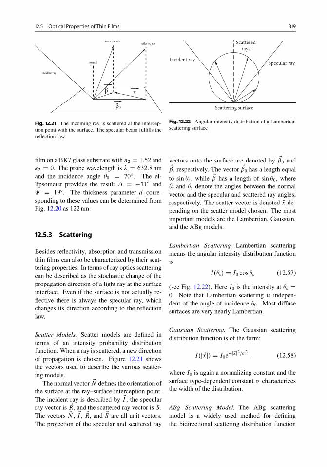
12.5 Optical Properties of Thin Films 319
x
β0
β
normal
scattered rayreflected ray
incident ray
Fig. 12.21 The incoming ray is scattered at the intercep-tion point with the surface. The specular beam fulfills thereflection law
film on a BK7 glass substrate with n2 D 1:52 and�2 D 0. The probe wavelength is � D 632:8nmand the incidence angle 0 D 70ı. The el-lipsometer provides the result � D �31ı and� D 19ı. The thickness parameter d corre-sponding to these values can be determined fromFig. 12.20 as 122 nm.
12.5.3 Scattering
Besides reflectivity, absorption and transmissionthin films can also be characterized by their scat-tering properties. In terms of ray optics scatteringcan be described as the stochastic change of thepropagation direction of a light ray at the surfaceinterface. Even if the surface is not actually re-flective there is always the specular ray, whichchanges its direction according to the reflectionlaw.
Scatter Models. Scatter models are defined interms of an intensity probability distributionfunction. When a ray is scattered, a new directionof propagation is chosen. Figure 12.21 showsthe vectors used to describe the various scatter-ing models.
The normal vector EN defines the orientation ofthe surface at the ray–surface interception point.The incident ray is described by EI , the specularray vector is ER, and the scattered ray vector is ES .The vectors EN , EI , ER, and ES are all unit vectors.The projection of the specular and scattered ray
Specular ray
Scatteredrays
Incident ray
Scattering surface
Fig. 12.22 Angular intensity distribution of a Lambertianscattering surface
vectors onto the surface are denoted by E0 andE, respectively. The vector E0 has a length equalto sin r , while E has a length of sin 0, wherer and s denote the angles between the normalvector and the specular and scattered ray angles,respectively. The scatter vector is denoted Ex de-pending on the scatter model chosen. The mostimportant models are the Lambertian, Gaussian,and the ABg models.
Lambertian Scattering. Lambertian scatteringmeans the angular intensity distribution functionis
I.s/ D I0 cos s (12.57)
(see Fig. 12.22). Here I0 is the intensity at s D0. Note that Lambertian scattering is indepen-dent of the angle of incidence 0. Most diffusesurfaces are very nearly Lambertian.
Gaussian Scattering. The Gaussian scatteringdistribution function is of the form:
I.jExj/ D I0e�jExj2= 2
; (12.58)
where I0 is again a normalizing constant and thesurface type-dependent constant characterizesthe width of the distribution.
ABg Scattering Model. The ABg scatteringmodel is a widely used method for definingthe bidirectional scattering distribution function

320 12 Measurements of Thin Layers After the Coating Process
(BSDF). BSDF is defined as the scattered radi-ance per unit incident irradiance, or
BSDF.i; �i; s; �s/ D dLs.s; �s/
dEi.i; �i/; (12.59)
where is the declination angle measured fromthe normal, and � is the azimuthal angle, andthe subscripts i and s refer to incident and scat-tered directions, respectively. The general termBSDF can refer to two separate functions, BRDFand BTDF, for reflective and transmitted distribu-tions, respectively.
BSDF Properties. For many optical surfaces,BSDF is independent of the incident direction ifit is plotted as a function of jExj D j E � E0j in-stead of angles of incidence. This quantity is thedistance between the scattered and unscatteredray vectors when projected down to the scatter-ing surface. It is generally adequate to use thisscattering model when the scattering is mainlydue to random isotropic surface roughness, andthe scale of the roughness is small compared towavelength of the light being scattered. Theseassumptions are generally valid for polished op-tical surfaces.
The ABg BSDF Model. When BSDF is plotted asa function of jExj, the resulting data may usuallybe fit to a function of the form
BSDF D A
B C jExjg : (12.60)
The ABg BSDF model is named such becauseof the three fit parameters A, B , and g. If g is0 (note that g may be any value, positive or neg-ative, but typically it is between 0 and 3), thenBSDF is constant in the direction cosine space:
BSDF D A
B C 1 ; (12.61)
and the resulting scattering is Lambertian.
12.5.4 Color
The color of thin films is determined by the spec-trum of the reflected or transmitted light. Color
00.20.40.60.8
11.21.41.61.8
2
350 400 450 500 550 600 650 700 750Wavelength(nm)
x(λ)
y(λ) z(λ)
Fig. 12.23 Standardized normal color matching functions
is strictly speaking not a pure physical quantitybut related both to physics and subjective percep-tion. However, it is possible to attribute to eachcolor a set of values which can be related to themeasurable light spectrum. The procedure howto calculate these color coordinates from a givenlight spectrum is regulated in various interna-tional standards. The most common standard isthe CIE (1932) standard [18].
Given the spectral radiant flux˚e.�/ of a lightsource, we first calculate the normalized spec-trum
S.�/ D ˚e.�/
˚e.�0/;
with �0 as the wave length of the maximum ofthe spectrum. If the spectral transmission orreflectivity of the sample is described by the nor-malized spectrum '.�/ the so-called tristimuluscoordinates are
X D k780 nmZ
380 nm
'.�/S.�/ Nx.�/ d�
Y D k780 nmZ
380 nm
'.�/S.�/ Ny.�/ d� ;
Z D k780 nmZ
380 nm
'.�/S.�/ Nz.�/ d� :
The standardized normal color matching func-tions Nx.�/, Ny.�/, and Nz.�/ are shown inFig. 12.23.

12.6 Spectrometers 321
The constant k is determined by the conditionfor a “white standard” ('.�/ D 1)
Y D k780 nmZ
380 nm
S.�/ Ny.�/ d� D 100 : (12.62)
The xy chromaticity coordinates are defined as:
x D X
X C Y C Z (12.63)
y D Y
X C Y C Z : (12.64)
With x and y the chromaticity can be visual-ized in a two-dimensional color map. The neutralpoint is at x D y D 0:33 (black, gray, white).Light characterized by a single wavelength iscalled a spectral pure color. The chromaticitycoordinates of pure colors comprise a trianglewithin the color map. Note that two differentspectra may have the same chromaticity coordi-nates causing the same color impression.
The radial distance within the color triangle tothe neutral point is a measure for the color satura-tion. The azimuthal position represents the colortone. The spectrally pure colors (determined byone wave length) are located on a line limiting thecolor triangle which comprises all possible col-ors.
12.6 Spectrometers
The spectral properties of thin films can be mea-sured with spectrometers. Although there isa large variety of different types and principles ofspectrometers, all spectrometers have in commona light source, some wavelength selecting com-ponent, and a light detector. The different wave-lengths of a spectrum can be separated into anangular spectrum (grating and prism spectrome-ters) or transformed into a time-dependent signalwhich is finally Fourier transformed (Fouriertransform spectrometers). Another importantclass are variable narrow-band optical filters likeFabry–Perot spectrometers. In thin film tech-nology mainly grating spectrometers and Fouriertransform spectrometers are used.
12.6.1 GratingMonochromatorsand Spectrometers
The dispersive element of a grating spectrometeris an optical grating. Although prisms have beenthe prototypes of dispersive components sinceIsaac Newton, today, they play only a major rolein UV spectrometry. The main reason is that op-tical gratings achieve a higher dispersion in thevisible and infrared regime. Another advantage isthat the dispersion of gratings is linear, whereasthe dispersion of prisms depends on the nonlineardispersion characteristics of the applied glass.
12.6.1.1 Optical GratingOptical gratings normally used in spectrometersare reflection gratings. Their substrates may beeither flat or curved. Also the line structuremay be parallel or curved depending on whetherthe grating is not only a dispersive but also animaging device. The simplest type of grating isa periodic line structure with a certain line sepa-ration (grating constant). The periodicity of thegrating is also given in lines per millimeter. Thestructure may be generated mechanically witha ruling machine that engraves the line structuresinto the substrate with a diamond tip. The sec-ond common method is to structure a photoresistby illuminating it with interfering laser light andtransfer the generated structure by anisotropicetching techniques into the substrate. If a lightbeam hits the grating the beam is spread into thevarious diffraction orders according to the gratingequation [3]
m� D �g.sin ˛in C sin ˛m/ ; (12.65)
with m as the number of the diffraction order, �the wavelength, g the grating constant, ˛in the in-cidence angle, and ˛m the diffraction angle ofthe diffraction orderm. According to Eq. (12.65)the diffraction angle of a certain order dependson the wavelength �. The angular dispersion ofthe grating is given by:
d˛
d�D m
g cos˛m: (12.66)

322 12 Measurements of Thin Layers After the Coating Process
αin
αb
αm
αB
g
Fig. 12.24 Blazed grating. The blaze angle is chosen sothat the respective diffraction order angle is equal to thereflection angle
The smaller the grating constant g the better theangular separation of the different wavelengths.The purpose of a grating in a spectrometer isto separate different wavelength components intodifferent angles. Thus, a high dispersion is oneaspect. The angular resolution of the gratingis also limited by the diffraction-induced diver-gence of the light beam. It is necessary toilluminate the grating with a beam bundle witha large diameter to minimize diffraction. Thewavelength resolution ı� of a grating is
ı� D �
mN; (12.67)
with N the number of lines illuminated by thelight beam. The beam must be broad to illumi-nate a high number of lines.
Besides the resolution of the spectrometer,also a broad spectral range should be covered bythe spectrometer. This is given by
�� D �min
m; (12.68)
with the minimum wavelength �min of the spec-trum.
Equation (12.65) determines the direction ofthe diffraction orders but it gives no informationabout the strength of the different orders. Thegrating would be ideal if all the light went intoa single diffraction order. In fact, this can beachieved with a blazed grating. The surface ofsuch a grating has a sawtooth shape as shownin Fig. 12.24. The surface sections between thelines are tilted by the blaze angle ˛B. The angle
detectorexitdiaphragm
entrancediaphragm
parabolicmirror
parabolicmirrorgrating
ellipsoidalmirror
lamp
diffractionorder
Fig. 12.25 Monochromator setup
of incidence ˛in must fulfill the blaze condition
˛in D 2˛B � ˛m : (12.69)
The incoming beam and the outgoing diffractionorderm are, of course, related by the grating con-dition Eq. (12.65). The blaze condition says thatthe incoming beam and the outgoing beam of thediffraction order fulfill the reflection law with re-spect to the tilted surface segments. With thegrating equation Eq. (12.65) and the blaze con-dition Eq. (12.69) one obtains
m� D �gŒsin ˛in C sin.2˛B � ˛in/� : (12.70)
The blaze condition can be fulfilled for a broadrange of wavelengths by choosing the appropriateangle of incidence. The diffraction efficiency ofa blazed grating also depends on the orientationof the polarization of the light. A high efficiencycan only be achieved if the polarization of thelight is parallel to the line orientation of the grat-ing.
Figure 12.25 shows the principal setup ofa monochromator. A bright light source suchas, for example, a discharge lamp is imagedwith an ellipsoidal mirror onto the entrance di-aphragm of the monochromator. The divergentlight emerging from the diaphragm is collimatedwith a parabola mirror. The collimated beam hitsa reflection grating. If the grating is blazed, inthe ideal case all light is diffracted into a specificdiffraction order. The diffracted light bundles ofthe different wavelengths are collimated and fo-cused onto the plane of the exit diaphragm of themonochromator.

12.6 Spectrometers 323
Only the bundle of one specific wavelength isfocused onto the exit diaphragm. The wavelengthcan be tuned by rotating the optical grating. Theresolution of the monochromator is determinedby Eq. (12.67). The number of grating lines illu-minated by the incoming collimated light beamdetermines the resolution. However, this rela-tion is only valid if the radius of the diaphragmrdiaphragm is so small, that the divergence angle 'of the light beam emanating from the entrance di-aphragm is determined by the diffraction relatedAiry formula:
rdiaphragm D 0:61 �NA; (12.71)
with the numerical aperture NA D sin '. In or-der to make optimal use of the light from thelight source, the angle of convergence of thelight focused onto the entrance diaphragm of themonochromator must also be equal to '.
An alternative to the application of ellipticaland parabolic mirrors in the system describedabove is to collimate the incoming light bya spherical mirror. Spherical mirrors are easier tomanufacture but generate astigmatism if they aretilted. After the collimated beam passes the grat-ing a second tilted spherical mirror focuses thelight onto the exit diaphragm. Additional astig-matism is contributed. The astigmatism causesa line shaped image of the entrance diaphragm.Fortunately, the line image is oriented normalto the angular dispersion of the grating. Inthis case, the entrance and exit diaphragms areslits.
The monochromator can be used as a wave-length tunable light source, which can be ap-plied, for example, to measure the wavelengthdependence of transmission or reflectivity of thinfilms. Monochromators are also used as tunablelight sources in spectral ellipsometry. In con-trast to monochromators, grating spectrometershave a fixed grating. The spectrum is detectedsimultaneously with a detector array (Fellgettadvantage). The disadvantages are that the res-olution is limited by the size and the number ofdetectors on the detector array. Also optical aber-rations limit the resolution and efficiency.
12.6.2 Fourier TransformSpectrometers
Grating spectrometers are very common becauseof their simple and robust design. CCD (charge-coupled device) line sensors make data acqui-sition easy. In the infrared regime, however,CCD lines are expensive or not available withthe necessary pixel number. In this field, fastFourier transform (FFT) spectrometers are pre-ferred. The concept of these spectrometers isbased on the Wiener–Khinchin theorem, whichrelates the Fourier transform of the temporal co-herence function of a light source to its opticalspectrum.
12.6.2.1 Temporal Coherence FunctionThe temporal coherence function of a light beamcan be measured with a Michelson interferom-eter, as shown in Fig. 12.26. The interferencesignal at the detector is measured as a function ofthe arm length difference �z. For this purpose,the arm length is changed by moving one mirrorat a constant speed.
The electrical field of the light beam is
E.t/ D E0.t/ e�i!t :
The amplitude E0.t/ is assumed to be complexand stochastic. The power density is
I D 1
2�0hE�.t/E.t/i (12.72)
reference mirrorMichelson
interferometer
moving mirrorlight sourceΔz/2
detectormeasuresRe(G(τ))
Fig. 12.26 Michelson interferometer setup

324 12 Measurements of Thin Layers After the Coating Process
D 1
2�0limT!1
1
2T
TZ
�TE�.t/E.t/dt ; (12.73)
with the impedance of the vacuum
�0 Dr�0
�0D 377� :
In favor of simplification one defines u.t/ DE.t/p2�0
such that
I D hu�.t/u.t/i :
At the detector of the Michelson interferometerthe amplitudes of the partial beams of the in-terferometer are superimposed. The amplitudefunction of one partial beam at the detector is
u1.t/ D 1
2u.t/ ; (12.74)
the other one is
u2.t/ D 1
2u.t C �/ ; (12.75)
where � D 2 �z=c is the difference in the timeof flight caused by the arm length difference�z.The intensity at the detector is then
IDet.�/ D h.u�1 .t/C u�
2 .t//.u1.t/C u2.t//i(12.76)
D 1
2I C .hu�
1 .t/u2.t/i C hu�2 .t/u1.t/i/ :
(12.77)
The temporal coherence function is defined as
G.�/ D hu�.t/u.t C �/i (12.78)
D limT!1
1
2T
TZ
�Tu�.t/u.t C �/dt :
(12.79)
Therefore,
IDet.�/ D 1
2I C 1
4.G�.�/CG.�// : (12.80)
With
G.�/ D1Z
�1u�.t/u.t C �/dt
we obtain with the correlation theorem of Fouriertransform theory
QG./ D FTfG.�/g D Qu�./ Qu./ D S./ ;with the Fourier transformation FT and the powerspectrum S./ of the light source. In otherwords, the Fourier transform of the coherencefunction is equal to the power spectrum S./ ofthe light source. This is the Wiener–Khinchintheorem, which allows to calculate the powerspectrum by Fourier transforming the coherencefunction.
In practice, the various Fourier transformspectrometers comprise a Michelson interferom-eter with variable arm lengths. The arm lengthdifference is changed with constant speed. Thelight from the two arms is superimposed at thedetector. The detector signal is amplified andrecorded as a function of time. The signal isFourier transformed by a microprocessor in orderto obtain the complex signal spectrum. The abso-lute square of the complex spectrum is the powerspectrum corresponding to the optical spectrumof the light source.
12.7 Microscopy
12.7.1 Optical Microscopes
A microscope typically consists of an objec-tive, a tube lens, and an eye piece, as shown inFig. 12.27. The object is in the front focal planeof the objective. The tube lens focuses the im-age into the back focal plane of the tube lens.
eye piece field lens objectivelens
Condenserlens
object lamp
tube lens
Fig. 12.27 Microscope schematic

12.7 Microscopy 325
The advantage of this geometry is that the raysfrom a object point are parallel behind the ob-jective, which is necessary when polarizers areinserted, e.g., in polarization microscopy. Theintermediate image is either transferred to an im-age capturing device like a CCD or a film, orit is looked at by an observer through an eyepiece. The eye piece plays the role of a magni-fier lens magnifying the intermediate image. Thetotal magnification is the product of the magni-fication of the objective in conjunction with thetube lens.
Besides the magnification, the main parame-ters characterizing an objective are its numericalaperture and the working distance (distance be-tween object plane and lens vertex). The numer-ical aperture is defined by
NA D n sin ˛ : (12.81)
The angle ˛ characterizes the divergence of thoserays emanating from an object point that areaccepted by the objective and focused to theintermediate image plane. n is the index ofrefraction of the medium between object and ob-jective. Normally this will be air with n D 1.To increase resolution immersion oil with n > 1
can be used to fill the space between the objectand the objective to increase the numerical aper-ture NA.
The aperture diaphragm of the objective isnormally located near the back focal plane of theobjective. It determines the aperture angle ˛ anddefines the exit pupil of the objective. If the di-aphragm is the back focal plane all chief raysfrom object points going through the center ofthe aperture diaphragm are parallel in the objectspace. This telecentric optics guarantees that theimage size does not change when the object isdefocused. This is useful in particular when themicroscope is used to measure distances withinthe object.
The eye piece consists of a field lens and theocular lens. The field lens is necessary to avoidthe key hole effect. Without the field lens theobserver’s eye pupil would accept only ray bun-dles with small angles relative to the optical axis.Thus, the observer would see only a small portion
of the object field. If the field lens is in place (itis normally located near the intermediate imageplane), the ray bundles emanating from periph-eral object points still enter the eye’s pupil. Therefractive power of the field lens is chosen suchthat the field lens together with the ocular lens(and optionally the tube lens) image the exit pupil(aperture stop) of the objective into the exit pupilof the microscope, which is situated tens of mil-limeters behind the eye piece at the position ofthe observers’s eye pupil.
Illumination. The object is illuminated by thecondenser optics. The light may transmit theobject if it is transparent (transmitted light mi-croscopy) or the object is illuminated through theobjective (incident light microscopy). The lightcone emanating from a point of the light sourceis collimated by the condenser lens. The paral-lel beam bundle hits the object. According toErnst Abbe any object can be thought of as be-ing a superposition of sinusoidal gratings. Thismodel is justified by the Fourier transform the-ory stating that any (integrable) function can berepresented as a superposition of harmonic func-tions. This is certainly true in particular for thefunction describing the spatial distribution of thetransmission of the object. For this reason it issufficient for the further discussion to focus ongrating objects. The parallel beam bundle hittingthe object is then split into the various diffrac-tion orders. The objective focuses the diffractionorders into the plane of the aperture stop, whichis located in the back focal plane of the objec-tive. The tube lens collimates the diffractionorders hitting the intermediate image plane asplane waves with different angles of incidence.As shown in Fig. 12.28 the first orders and thezeroth order interfere. We may ignore the inter-ference between the first orders when we assumethat the grating is weak such that the zeroth orderis strong compared to the first orders.
The interference pattern can be interpreted asthe image of the optical grating. The distance ofthe maxima of the interference pattern is deter-mined by the diffraction angle , given by the

326 12 Measurements of Thin Layers After the Coating Process
Fig. 12.28 Coherent illu-mination
object aperture intermediateimage
lightsource
condenser objective tube lens
+1 0
-1
Fig. 12.29 Oblique illumi-nation
object aperture intermediateimage
lightsource
condenser objective tube lens
0
-1
diffraction equation of the optical grating
g sin D � : (12.82)
Figure 12.28 also shows that interference canonly occur when the first diffraction order is fittedinto the aperture stop. The radius a of the aper-ture stop determines the numerical aperture NAof the objective. It is
NA D sin max ;
with max as the diffraction angle, where the firstdiffraction order still passes the aperture stop.With paraxial approximation we have NA Da=f . The resolution limit is achieved when thegrating constant g is so small that
ggrenz D �
NA:
In Fig. 12.28 the illuminating wave hits the grat-ing perpendicularly. The first diffraction gratingstill passes the aperture stop.
The resolution limit can be improved by a fac-tor of 2 by choosing oblique illumination, asshown in Fig. 12.29.
The minimum grating constant gmin, whichcan still be resolved is then
gmin D �
2 NA: (12.83)
So far we have discussed point-like light sources.Normally extended light sources such as, for ex-ample, halogen lamps are used. Figure 12.29shows the zeroth and first order for the case ofan off-axis light source point. The interferencepatterns generated by the individual points of thelight source in the intermediate image plane areidentical. Because of the symmetric setup theexit angles 0; �1 of the respective diffraction or-ders at the grating and the angles of incidence atthe intermediate image plane are equal. In a realmicroscope the magnification is higher than 1.Nevertheless, the magnified interference patternsfrom each point of the light source are still identi-cal. In other words, the contrast is not diminishedwhen an extended light source is used. In addi-tion, the advantage of Koehler’s illumination isthat an extended light source provides more lightthan a point-like source. The highest efficiency isachieved when the image of the light source fillsthe aperture of the objective. Therefore, the nu-merical aperture of the condenser should be equalto the numerical aperture of the objective. An-

12.7 Microscopy 327
other advantage is that the maximum resolution istwice the resolution achievable with coherent il-lumination because also the oblique zeroth orderwaves and their higher diffraction orders con-tribute to the imaging process.
Useful Magnification. The magnification of themicroscope objective is noted there. This meansthe ratio between the size of the image of the ob-ject in the intermediate image plane and the sizeof the object. If an eye piece is used, or a camera,the image size can be magnified further. In prin-ciple there are no limits, in particular when theimage is recorded electronically. The distance ofthe above-mentioned interference fringes in theintermediate image plane corresponding to theresolution limit is, according to Eq. (12.83):
� D �
2 NAMobj ; (12.84)
with the magnification of the objective Mobj.With an eye piece the magnification Mep is givenby the magnification of a magnifier lens:
Mep D s
f; (12.85)
with the normal visual distance s D 0:25m andthe focal length f of the eye piece. The resolu-tion of the human eye is ıeye D 10. Therefore, themagnification of the eye piece is sufficient as longas the eye can resolve the magnified structures ofthe intermediate image of the microscope. Thefocal length f of the eye piece is then:
f D �
ı:
With � D 550 nm and Eqs. (12.84), (12.85) fol-lows
Mges DMepMobj D 300NA :
Because the resolution of the eye is normallyworse than 10 the recommended useful magnifi-cation is between 500NA and 1000NA.
Polarization Microscopy. Because thin films arenormally homogeneous, the polarization of po-larized light is not changed in transmitted light
microscopy. However, dust particles or mechan-ical stress may depolarize or change the polar-ization state. In a polarization microscope thespecimen is illuminated with linearly polarizedlight. For this purpose, a linear polarizer is nor-mally located underneath the condenser optics,which can be flipped in and out. Behind the ob-jective another polarizer (analyzer) is placed withan orientation perpendicular to the orientation ofthe polarizer of the condenser. If the specimendoes not change the state of polarization, no lightreaches the image plane. In the case of opticallyanisotropic materials, the reflected light (incidentlight microscopy) or the transmitted light (trans-mitted light microscopy) is elliptically polarized.In a polycrystalline specimen, the effect may varystrongly from one crystallite to another, so thatthe crystallite structure appears with high con-trast in the intermediate image. Scattering objectdetails often display a depolarizing effect, whichmeans that they appear brighter in the image thansmooth objects. Polarization microscopes re-quire specially selected objectives and condenserlenses that exhibit as little strain-induced bire-fringence as possible. The analyzer and polarizershould be arranged in a parallel ray path.
Dark Field Microscopy. As discussed above po-larization microscopy is one tool to image scat-tering disturbances on thin films. An evenstronger method is dark field microscopy. Ina dark field microscope only the light diffractedby the object reaches the image plane. Theray path of a dark-field microscope is shownin Fig. 12.30. The light source is imaged intothe plane of the ring-shaped aperture stop of thecondenser. Figure 12.30 shows the light pencilemanating from a point of the intermediate im-age of the light source in the ring aperture.
The condenser lens collimates the light. Theparallel light bundle passes the object plane butdoes not enter the objective lens. However, ifthere is a scattering particle in the object planepart of the illuminating light is scattered intothe objective and is focussed into the imageplane. This makes it possible to make visiblevery weak objects that would be swamped by the

328 12 Measurements of Thin Layers After the Coating Process
image
scattered light
objective
specimen
condenser lens
ring aperture
illumination
Fig. 12.30 Dark field illumination
undiffracted light in normal bright field illumina-tion.
Interference Microscopy. Thin film surfaces areoften reflecting and plane structures. The topog-raphy is very flat. Deviations from the planereference are in the nanometer range. A planewave reflected at this surface carries the heightdeviations of the sample in their wave fronts.In interference contrast microscopy the phasedistribution impressed on the illuminating wavefield by a phase object is imaged. The mi-croscope interferometers include the Mireau andLinnik interferometer, the differential interfer-ence contrast (Nomarski DIC), and the Inter-phako method. Figure 12.31 shows the schematicsetup of a Mireau interferometer objective.
The Mireau interferometer consists of an ob-jective lens and a beam splitter plate between lensand object. Part of the incident light is reflectedby the beam splitter and is focused on a smallmirror in front of the objective lens. The otherpart is reflected by the object. If the object sur-face height changes or the object is defocusedby �z, the optical path length of the referencepath changes by �s. It is �s D 2s1 � s2 with
reference mirror
objective
beam splitter
defocused object
objectθ z
θθ
s2
s1
Fig. 12.31 Mireau interference microscope
s1 D �z= cos and s2 D 2 tan sin �z. There-fore,
�s D 2�z cos ; (12.86)
with the angle of incidence of the referencebeam. The resulting phase shift of the probebeam is
�' D k �s D 2k�z cos ; (12.87)
with k D 2�=�. A phase shift of 2� and,therefore, a shift of the interference pattern byone period is achieved when the sample surfaceheight changes by
�z2� D �
2 cos : (12.88)
Figure 12.32 shows an example.
Differential Interference Contrast (NomarskyDIC). The illuminating wave shown inFig. 12.33 is linearly polarized. It strikes a Wol-laston prism, splitting the principal ray of theilluminating wave into two rays.
The Wollaston prism is located in the back fo-cal plane of the objective such that the object isilluminated by two foci with the spacing d . The

12.7 Microscopy 329
Fig. 12.32 Interferogram of the edge of a ZnO film ona glass plate. The fringe separation corresponds to �=2 D275 nm. From the fringe shift a step height of 105 nm canbe derived
reflected waves experience a phase shift differ-ence
ı D 4��z=� (12.89)
due to the step structure of the object shownin Fig. 12.33. Both waves are recombined in
image
light source
Wollaston prism
objective
object planed
Fig. 12.33 Differential interference contrast microscopy(DIC)
the Wollaston prism and superimposed in the in-termediate image, where they interfere. Withthis method, phase differences between adjacentobject points separated by the distance d arerepresented as brightness contrast in the interme-diate image. Thus, the contrast of this techniquedepends on the change of the object topography.It is a very sensitive method to image, for exam-ple, crystallite boundaries on thin films or verysmall step heights.
12.7.2 Electron Microscopy
Electron microscopes are important tools in thinfilm technology, first of all because of theirhigh resolution. Scanning electron microscopes(SEM) can show surface structures without com-plicated preparation techniques. The electronbeam can be used to excite atoms to emit X-rays. The typical spectra can be used to iden-tify the element distribution on the surface andwithin the bulk material with nanometer resolu-tion. Transmission electron microscopy (TEM)provides even resolution, which allows resolutionof individual atoms. More important informationis the crystallite structure which can be monitoredby electron beam diffraction. A very importantpart of electron microscopy is sample prepara-tion. For example, the resolution of atoms withTEM can only be achieved if the sample is verythin. Different layers of a thin film probe canonly be distinguished with SEM if a proper cross-section of the film can be prepared. Particularlyin the last few years, ion beam etching has beenestablished as a very elegant and universal prepa-ration technique in practical electron microscopy.
Electron microscopes use electron beams togenerate images with very high resolution. Thebeam is focused by magnetic and electrostaticfields guiding the electrons with the Lorentzand Coulomb forces. The setup of elec-tron microscopes can be divided into electronsource, condenser, objective, and projective sys-tem.
Although the particle character of electronsdetermines most technical characteristics of elec-tron microscopy, the ultimate resolution limit of

330 12 Measurements of Thin Layers After the Coating Process
electron microscopes is determined by the wavecharacter of the electrons. The minimum spatialdistance dmin that can be resolved corresponds tothe resolution limit in light microscopy:
dmin D �de Broglie
2˛;
with the de Broglie wavelength �de Broglie and 2˛as the angle of divergence of the focused electronbeam. The de Broglie wavelength depends on theelectron mass me and the electron velocity v:
�de Broglie D h
me v :
In contrast to photons, which propagate withthe constant speed of light, electrons can be ac-celerated or reduced by appropriate electrostaticpotentials. As a consequence, the wavelengthand thus the resolution of the microscope can beeasily changed by changing the electron speed.On the other hand, in electron microscopes thenumerical aperture angle ˛ is much lower com-pared to numerical apertures NA used in lightmicroscopy because the aberrations of magneticlenses increase dramatically with ˛.
Electron Source. The electrons for the beam ofan electron microscope are generated by an elec-tron gun. It emits electrons (e.g., thermally) intothe vacuum and accelerates them between a cath-ode and an anode. The gun brightness is
ˇ D j
�˛2; (12.90)
with the beam current density j and the beamdivergence angle 2˛. The gun brightness ˇ cor-responds to the radiance Le of an optical lightsource. The current density of the cathode emis-sion can be estimated from Richardson’s law
j D AT 2 exp.��=kT / ; (12.91)
where k D 1:38 10�23 J=K is Boltzmann’s con-stant, T is the cathode temperature, � is thework function of the cathode, and A is a constantdepending on the cathode material. Therefore,
external potential
potential
internal externalcathodesurface
ooeff
Fig. 12.34 The work function � is reduced by the Schot-tky effect. The thick line shows the effective potentialbarrier at the cathode with the reduced work function �eff
a high current density j can be achieved witha high cathode temperature T and a cathode ma-terial with a low work function �. Applyinga high field strength E to the cathode the workfunction � can be further reduced by the Schot-tky effect, leading to an effective work function
�eff D � �se3jEj4��0
: (12.92)
The Schottky effect is caused by the mirrorcharges induced by the emitted electrons in themetallic cathode. An electron leaving the cath-ode still experiences an attractive force. Thus,the potential barrier is not a step function. To-gether with the superimposed external electricalfield between cathode and anode the potentialbarrier shown in Fig. 12.34 is received.
Most metals melt before they reach a suffi-ciently high temperature for thermionic emission.With tungsten working temperatures T between2500 and 3000 K can be achieved. Its meltingpoint is at 3650 K. Lanthanum hexaboride (LaB6)is used as cathode material at lower temperaturesT D 1400–2000 K because its work function isonly 2.7 eV (4.5 eV for tungsten).
The work function of the field emission guncan be further reduced with a ZrO2 coating ap-plied to the surface of the gun tip. These Schottkyfield emission guns show a better stability com-pared to cold FEGs (field emission gun). How-ever, the source size is slightly larger.

12.7 Microscopy 331
Uheat
cathodeWehneltcylinder
crossover
anode
electron beam
Fig. 12.35 Thermionic gun
Tungsten sources in thermionic guns are mostwidely used because of their high current stabil-ity and relatively low cost. The thermionic gun isa triode consisting of a negatively charged tung-sten wire cathode heated resistively, a Wehneltcylinder, and an anode, as shown schematically inFig. 12.35. These components are maintained atdifferent potentials, giving a beam energy of 0.1–40 keV for SEMs and 100–400 keV for TEMs.The Wehnelt cylinder acts as an electrostatic lensgenerating an intermediate image of the cathodewith a diameter d0 (crossover). The distributionof the electron energy f .E/ is determined by theMaxwell-Boltzmann distribution and, therefore,by the cathode temperature T
f .E/ D E
.kT /2exp.�E=.kT // ; (12.93)
with the Boltzmann constant k. The full-widthhalf maximum of this distribution is �E D2:45kT . For a cathode temperature of T D2500K the half-width is�E D 0:5 eV. The typi-cally observed energy spread is, however, 1–2 eV.This can be explained by the repulsive Coulombinteraction of the electrons in the crossover zone(Boersch effect).
It is desirable to have a low energy spread�Eto minimize chromatic aberration. Therefore,LaB6 cathodes are preferable because they canbe operated at lower temperatures. FEGs providea high gun brightness. Because they are oper-ated at ambient temperature their energy spread
incoming ray fan
coil
rotated ray fan
Feφ
Fig. 12.36 Electron lens. The electrons follow spiral-shaped trajectories through the lens. A parallel incomingray fan is focused and rotated by the magnetic lens
�E is low. This is important for high resolu-tion SEM and TEM imaging and microanalysis.The small source size of FEGs also guaranteesa high spatial coherence for special TEM imag-ing techniques such as atomic structure imagingand electron holography.
Electron Lens. Electron beams can be focusedwith magnetic and electrostatic fields. In mag-netic fields the trajectory of electrons is deter-mined by the Lorentz force:
F Lorentz D �e.v �B/ ;
with electron velocity v, electron charge e, andthe magnetic field B of the electron lens. Anelectron beam can be focused by a magneticdipole field generated by a magnetic coil asshown in Fig. 12.36.
The electrons follow spiral-shaped trajectoriesthrough the lens. A parallel incoming ray fan isfocused and rotated by the magnetic lens. The Bfield along the axis is
Bz D B0
1C .z=a/2 ; (12.94)
where a is the half-width at half maximum ofBz.z/ and B0 is the maximum field at the lens
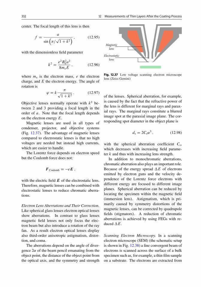
332 12 Measurements of Thin Layers After the Coating Process
center. The focal length of this lens is then
f D a
sin��=p1C k2
� ; (12.95)
with the dimensionless field parameter
k2 D e2B20a
2
8meE; (12.96)
where me is the electron mass, e the electroncharge, and E the electron energy. The angle ofrotation is
' D k �p1C k2 : (12.97)
Objective lenses normally operate with k2 be-tween 2 and 3 providing a focal length in theorder of a. Note that the focal length dependson the electron energy E.
Magnetic lenses are used in all types ofcondenser, projector, and objective systems(Fig. 12.37). The advantage of magnetic lensescompared to electrostatic lenses is that no highvoltages are needed but instead high currents,which are easier to handle.
The Lorentz force depends on electron speedbut the Coulomb force does not:
F Coulomb D �eE ;
with the electric field E of the electrostatic lens.Therefore, magnetic lenses can be combined withelectrostatic lenses to reduce chromatic aberra-tions.
Electron Lens Aberrations and Their Correction.Like spherical glass lenses electron optical lensesshow aberrations. In contrast to glass lensesmagnetic field lenses not only focus the elec-tron beam but also introduce a rotation of the rayfan. As a result electron optical lenses displayalso third-order anisotropic astigmatism, distor-tion, and coma.
The aberrations depend on the angle of diver-gence 2˛ of the beam pencil emanating from theobject point, the distance of the object point fromthe optical axis, and the symmetry and strength
Magneticlens
Electrostaticlens
Fig. 12.37 Low voltage scanning electron microscopelens (Zeiss Gemini)
of the lenses. Spherical aberration, for example,is caused by the fact that the refractive power ofthe lens is different for marginal rays and parax-ial rays. The marginal rays constitute a blurredimage spot at the paraxial image plane. The cor-responding spot diameter in the object plane is
ds D 2Cs˛3 ; (12.98)
with the spherical aberration coefficient Cs,which decreases with increasing field parame-ter k and thus with increasing lens strength.
In addition to monochromatic aberrations,chromatic aberration also plays an important role.Because of the energy spread �E of electronsemitted by electron guns and the velocity de-pendence of the Lorentz force electrons withdifferent energy are focused to different imageplanes. Spherical aberration can be reduced bylocating the specimen within the magnetic field(immersion lens). Astigmatism, which is pri-marily caused by symmetry distortions of themagnetic lenses, can be corrected by quadrupolefields (stigmators). A reduction of chromaticaberrations is achieved by using FEGs with re-duced �E.
Scanning Electron Microscopy. In a scanningelectron microscope (SEM) (the schematic setupis shown in Fig. 12.38) a fine convergent beam ofelectrons is scanned across the surface of a bulkspecimen such as, for example, a thin film sampleon a substrate. The electrons are extracted from

12.7 Microscopy 333
first crossover (1μm)
second crossover (3μm)
third crossover (3μm)
focused electron beam
condenser lens 1
condenser lens 2
focusing lens
electron probe (30 nm)
Fig. 12.38 Scanning electron microscope setup
the cathode’s thermionic source and focused witha Wehnelt cylinder into the first crossover witha diameter of about (30 µm). A mechanicalaperture stop allows us to change the size anddivergence angle of the beam determining theprobe aperture ˛p at the specimen. The probeaperture ˛p, the probe diameter dp, and the elec-tron probe current Ip are not independent becauseof the constancy of the gun brightness in the elec-tron optical system (Lagrange theorem). There-fore, they cannot be changed independently.
The first crossover is further demagnified bytwo condenser lenses until the third crossoverreaches a diameter of about 0.3 µm. Finally, thebeam is focused onto the specimen by the objec-tive lens to a probe diameter in the nanometerrange. The probe is scanned across the sam-ple with scanning coils periodically deflecting thebeam in x and y directions. The electrons emit-ted from the probe–specimen interaction zoneare gathered by detectors. The detector cur-rent is recorded and displayed. The SEM hasa high depth of field because the probe aper-ture ˛p is rather low. Another advantage is thatonly minimal specimen preparation is necessary.Normally, the specimens must be coated with
a conducting film (e.g., gold) to avoid chargingof the specimen through the high energy electronbeam. However, also isolators can be imagedif the beam energy is low enough so that emit-ted electrons are replaced by electrons from theprobe beam.
The electrons of the focused probe in theSEM interact elastically and inelastically with thespecimen. The elastic scattering processes areRutherford and Mott scattering. Inelastic scatter-ing is caused by inner and intra-band transitionsin the valence and conduction band, by innershell excitation and plasmon excitation. The scat-tered electrons remitted from the specimen canbe detected. Back scattered electrons (BSE) aregenerated in a zone that is much larger and deeperthan the focus spot. They are multiply scatteredelectrons of the probe beam with a very broad en-ergy distribution. In addition to BSE, secondaryelectrons (SE) are also important for image gen-eration. They are generated directly at the probebeam focus.
Conventionally, the boundary energy betweenSE and BSE electrons is 50 eV. The SE electronsare further classified into SE1 and SE2 electrons.SE1 electrons are secondary electrons that aredirectly excited by the primary electrons to anenergy level high enough to overcome the workfunction. Their contribution to the SE signal isabout 20–50 % and their energy is typically 2–5 eV. SE1 electrons emanate from a film that isonly a few nanometers thick below the specimensurface and are scattered back into a very smallangle. Therefore, SE1 electrons are capable offorming an image of the surface (topographiccontrast). SE2 electrons are secondary electronsgenerated by BSE electrons. Their energy ishigher and they emanate from a volume withinthe specimen which is much broader and deeperthan the probe focus. They are also scattered intoa much broader angle than the SE1 electrons.
X-Ray Microanalysis. The incident electronbeam may excite electrons in an inner shell ofspecimen atoms causing its ejection and result-ing in the formation of an electron hole withinthe atom’s electronic structure. An electron froman outer shell soon fills the hole, and the excess

334 12 Measurements of Thin Layers After the Coating Process
energy of that electron is released in the form ofan X-ray photon. The energy spectrum of theseX-ray photons is characteristic for the specific el-ement.
X-ray spectrometers can be interfaced toa SEM to obtain elemental data from the beam–specimen interaction where X-rays with a char-acteristic spectrum are emitted from specimenatoms that have been excited by the probe beam.
An energy dispersive X-ray spectrometer usesa cooled, reverse-bias p-i-n Si(Li) crystal or anintrinsic Ge crystal. Absorption of each X-rayphoton leads to the formation of electron–holepairs, which are swept away by the applied bias toform a charge pulse. Each charge pulse is propor-tional to the energy of the incoming X-ray photon.This type of spectrometer is very efficient for X-ray photon energies in the range of 2.5–15 keV,but inefficient with low resolution at low energies(< 1 keV). In this case, a wavelength dispersivespectrometer (WDM) is preferable; it uses an an-alyzing crystal to diffract X-rays of specific wave-length � according to Bragg’s law
m� D 2d sin ; (12.99)
where d is the diffracting plane spacing, m isthe diffraction order, and the angle of inci-dence of the X-ray beam on the crystal. Thediffracted X-rays are detected by a proportionalcounter. A slit aperture in front of the detectorselects a certain diffraction angle. The angle ofincidence , which is related to � by Eq. (12.99),is changed by rotating the crystal. The detectorsignal is registered as a function of and, there-fore, according to Eq. (12.99) as a function of �,providing a high resolution X-ray spectrum.
The focused electron beam generates X-raysfrom a small interaction volume within the spec-imen, generally 1 µm in depth and width. Withthis method, it is possible to detect a very smallquantity of an analyte (< 10�16 g).
Low Voltage SEM. High energy electron beamsare used to avoid chromatic aberration becausethe thermal energy spread of the electrons issmall compared to the electron energy. An-other reason is to achieve high beam brightnessas discussed above. As a result, high resolu-
tion and small probe diameters are attainable.Low density specimens with no conductive coat-ing require very low electron energies in orderto achieve a charge equilibrium on the specimensurface. Besides the increase of the chromaticaberration the electron interactions at crossoverpoints in the electron optical system further en-hance the energy spread (Boersch effect). Alsothe beam brightness is limited.
The SEM optics shown in Fig. 12.39 avoidsthe disadvantages of a low voltage electron mi-croscope by avoiding crossovers between elec-tron source and specimen. The main improve-ment is the combination of a booster system, con-stant high voltage (10 kV) between source andobjective, and a chromatic electrostatic/magneticlens, decelerating the electron beam. Both spher-ical and chromatic aberration are reduced whenthe electron energy is reduced. This is achievedby the electrostatic field of the electrostatic lens,which decelerates the electrons to low energieswhen they reach the magnetic field lens.
In addition the energy spread of electrons isreduced by using a field emission tip (cathode).The Schottky emitter has a virtual source diam-eter of 15 nm. No real crossover (only virtualcrossover) exists, thus, reducing the Boersch ef-fect.
The secondary electrons (SE) generated di-rectly at the specimen surface are emitted into theelectrostatic lensand focusedby theobjectivesuchthat the electron trajectories optimally reach an an-nular SE detector (in-lens detector) located withinthe objective lens. The BSE electrons emanatingfrom deeper zones of the specimen are success-fully suppressed by this arrangement. Thus, theSE image describes the specimen surface muchmore precisely than an image acquired with a clas-sical detector located in the specimen chamberwhich collects both SE and BSE electrons.
The left-hand part of Fig. 12.40 shows theimage of an underetched silicon carbide sampleacquired with an Everhart Thornley detector. Theimage shows deep etching grooves, covered bya very thin film. The right-hand side pictureshows the same detail acquired with an in-lensdetector selecting primarily SE electrons gener-ated at the surface of the thin film.

12.7 Microscopy 335
Fig. 12.39 Gemini scan-ning electron microscopesetup
Schottky FE cathode
Extractor anodeSecond anode
Aperture changer
Field lens
In-lens SE-detector
Beam booster
Magnetic lens
Scan coils
Electrostatic lens
Specimen
UL
U0UEX
Fig. 12.40 In-lens detection
Transmission Electron Microscopy. The left-hand side diagram of Fig. 12.41 shows theschematic setup of a transmission electron mi-croscope. An area with a diameter of 1–10 µmof a thinned specimen is irradiated with a nearlyparallel beam of high energy electrons (100–400 keV) emitted from the electron gun and col-limated by the condenser lens. The objectivelens forms an intermediate image by collectingelectrons that have either been transmitted withlittle or no change in angle, as in bright fieldimaging (BF), or scattered by the specimen, asin dark field imaging (DF). The intermediate im-age is further magnified by the projector lens
system generating the final image onto the view-ing screen or CCD. The image generation canbe understood in terms of Abbe’s theory of themicroscope because of the wave nature of theelectrons (de Broglie waves). The plane electronwaves from the condenser are diffracted by thespecimen. This consists of atoms comprising pe-riodic structures or at least structures that can bethought of as being composed of periodic struc-tures according to Fourier theory. The diffractionorders are superimposed in the image plane bythe projection system generating an interferencepattern that represents the image of the sample.
The image of the diffraction orders (diffrac-tion image) can be directly viewed by choosingan appropriate coil current of the projector lenssystem to focus the diffraction image onto the im-age plane (Fig. 12.41).
The basic difference of image formation inlight microscopy and TEM is that specimens forlight microscopy can be prepared with a thick-ness as small as the light wavelength. Specimensfor TEM are to be regarded as three-dimensionalbulk structures because the de Broglie wave-

336 12 Measurements of Thin Layers After the Coating Process
Fig. 12.41 Left: imageformation of the transmis-sion electron microscopeas a superposition of inter-fering diffraction orders inthe image plane. Right: byreducing the power of theprojector lens the diffrac-tion orders are focused onthe “image” plane. Thisdiffraction diagram canbe used to investigate thecrystal structure of thesample
electron gun
condenser system
specimen
objective lens
projector lens
order -1
order -1
order 0
order 0order +1
order +1
image diffraction image
Fig. 12.42 a Crystal lat-tice, b reciprocal lattice a
gd
b
g
1/d1/a
1/b
a b
length is smaller than the sample thickness.Therefore, a parallel electron beam passing evena thin single crystal specimen is diffracted ac-cording to Bragg’s law, which describes diffrac-tion by a three-dimensional periodic lattice struc-ture. The Bragg condition for diffraction is
k� k0 D g : (12.100)
Here k0 is the k-vector of the incoming electronwave with length jk0j D 2�=�, k the k-vectorof the outgoing diffracted electron wave withthe same length jkj D jk0j (but different di-rections), and g a reciprocal lattice vector withlength 2�=d normal to the lattice planes withspacing d ; � is the de Broglie wavelength of theelectrons.

12.8 Permeation 337
k
gkO
reciprocal latticeEwald sphere
Fig. 12.43 Ewald sphere. Condition for Bragg reflection
Figure 12.42 shows the geometrical situation.The reciprocal lattice is given by the normal vec-tors g of the lattice planes of a crystal. The lengthof g is 2�=d with d as the corresponding lat-tice plane distance. The sphere with radius k inFig. 12.43 is the Ewald sphere. Due to the mo-mentum conservation law we have
g D k0 � k : (12.101)
Because k0 and k have the same length, Bragg’slaw can be written with Eq. (12.101) as
jgj2D jkj sin (12.102)
or
� D 2d sin ; (12.103)
with 2 the angle between k0 and k. The angle is known as the Bragg angle. Thus, the directionsof the various diffraction orders characterized bythe directions of k represent the various latticeplane orientations of the crystal specimen.
12.8 Permeation
For thin film technology permeation is of funda-mental importance. The metallic, glass, or rubberwalls of vacuum chambers or pipes are more orless permeable to gases. The permeation mecha-nism can be atomic or molecular. For monatomic
gases the permeation gas flow is calculated as:
IP D AP p2 � p1d
; (12.104)
whereIP is the permeation gas flow,A is the surface,P is the permeation constant,p1, p2 are the gas pressures at the two surfaces
of the solid body, andd is the thickness of the solid body.
With diatomic gases dissociation usuallyarises. We then obtain the following equation:
IP D APpp2 �pp1d
: (12.105)
The permeation constant is gas and material-dependent and increases exponentially with ris-ing temperature.
At ambient temperature and higher tempera-tures up to some hundreds of degrees for glassand metals – exceptions are silver for oxygen andpalladium for hydrogen – the permeation is ex-tremely low and does not have any considerableinfluence on the pressure ratios in a vacuum re-cipient, but it is not negligible for elastic seals.The permeation of elastic seals determines the at-tainable final vacuum pressure beside the pump-ing speed of the pumps [15]. Permeation is alsoimportant for food packaging [16].
The permeation of atmospheric gases throughmetal walls does not include rare gases (He, Ar,Ne, Kr, Xe), since no noble gas diffuses throughmetals at any temperature under purely thermalactivation. There can be penetration of noble gasions under a potential gradient, or noble gases canbe formed in situ in the metal interior by a nucleardisintegration process.
The permeability of aluminum for hydrogen isvery small. It is negligible in all cases except inultrahigh vacuum chambers, or with thin-walledchambers heated at high temperatures. Copperis a metal with low permeability for all gases,including hydrogen. Nickel has a higher per-meability for hydrogen. The permeation of hy-drogen through steels increases with increasingcarbon content; low carbon steels are thus pre-ferred as vacuum containers. Organic polymersare permeated by all gases, including noble gases.

338 12 Measurements of Thin Layers After the Coating Process
12.8.1 Measurement Principles
With all measuring instruments, the foil or filmto be examined is clamped gas-tightly betweentwo chambers. A chamber contains the measur-ing gas, and the part of the gas that permeatesthrough the sample is quantitatively measured inthe second chamber [25].
In principle, three measuring methods areused:� Absolute pressure measuring method� Isostatic measuring method� Quasi-isostatic measuring method.
12.8.1.1 Absolute Pressure MeasuringMethod
This measuring method is only used with testgas in two chambers. The permeation processis based on the absolute pressure gradient be-tween the two chambers. Figure 12.44 [25]shows the different absolute pressure measuringpossibilities.
Figure 12.45 shows a calibration device withmeasurable variable pressure and volumes. Thepermeation constant P can increase the curvewhen a steady state of the gas passage prevailsover the linear part of the pressure.
a
b
c
Manometric-volumetric
dn–Vdp+pdV
Volumetricdn–pdV
Manometricdn–Vpd
pa
p1
Fig. 12.44 Absolute pressure measuring methods. pB
atmospheric pressure, p1 pressure in the measuring cham-ber a test gas, b bubble counter, c detection system
0102030405060708090
a b
c e d
g
f
Fig. 12.45 Calibration device with measurable variablepressure and measurable variable volume. a gas inlet,b gas outlet, c sample (foil), d seal, e filter paper, f pump,g ventilation
The permeation constant P is calculated withconstant volume as:
P D T0VM .p2 � p1/ dT p0A .pG � p1/ t ; (12.106)
wherep0 1013 mbar,T0 273 K,T is the temperature of the measuring chamber,VM is the volume of the measuring chamber,A is the surface of the samples (foils) to be ex-
amined,d is the thickness of the foil to be examined,pG is the pressure in the gas supply chamber,p1 is the pressure in the measuring chamber at
the beginning of the measurement,p2 is the pressure in the measuring chamber at
the end of the measurement, andt is the duration of the measurement.

12.9 Mechanical Stresses in Thin Films 339
Fig. 12.46 Pattern ofa measuring instrumentworking according to theisostatic principle. a testgas, b feed gas, c sensor
Gas-specific(e.g. electrolysis cell,
O2 analyzer, IR detectors)
Heat conductivity measuring cell
Radiometricdetection
a
b
a
cb
12.8.1.2 Isostatic Measuring MethodWith the isostatic measuring method differentgases can be in both chambers in addition to themeasuring gas. These gases may not react withthe sample, and the total pressure must be equalon both sides of the sample. Moreover, a pres-sure gradient for the measuring gas must exist.Both chambers are in pressure balance with theexternal atmosphere. Figure 12.46 schematicallyshows a measuring instrument functioning ac-cording to this principle.
12.8.1.3 Quasi-Isostatic MeasuringMethod
With this method one of the two chambers islocked, clamped between the sample. Pressureequalization with atmospheric air or with theother chamber does not take place. In one ofthe two chambers a little over- or low pressuredevelops, which is connected with an easy deflec-tion of the sample. The permeated mass of thegas is determined by means of gas chromatogra-phy [25].
12.9 Mechanical Stressesin Thin Films
12.9.1 Introduction
Mechanical stresses in thin films influence theoptical, electrical, magnetic, mechanical andchemical properties, and the adhesion.
The stresses in thin films consists of the twoparts T and i :
D T C i : (12.107)
T are thermal stresses, which develop if the co-efficients of dilatation of film and substrate aredifferent and if the measurement takes place atanother temperature than with the coating proce-dure.
We have:
T D ES .˛S � ˛U/ .TB � TM/ ; (12.108)
whereES is the modulus of elasticity of the film,˛S is the middle thermal coefficient of expansion
of the film,˛U is the middle thermal coefficient of expansion
of the substrate,TB is the substrate temperature during the coat-
ing, andTM is the substrate temperature during the mea-
surement.Factors are residual gas insertion into the de-
veloping film during the coating, condensationvelocity, substrate temperature, film thickness,film structure, and bias [26, 27]. By insertionof residual gas atoms into the film, compressivestress can be converted into tensile stress [28],Fig. 12.47. The stresses are measured as a thinsubstrate from quartz or glass is coated and thestress due to the deflection of the substrate ismeasured. The separation of the two parts T and

340 12 Measurements of Thin Layers After the Coating Process
Fig. 12.47 Argon pres-sure at the transition ofcompression stresses totensile stresses. A cylindricmagnetron cathode wasused for the film genera-tion. The argon pressurewith the recording of thelower curve amounted to1:3 � 10�3 mbar
10
6
4
2
1
0.6
0.4
0.2
0.1
0.06
0.04
0.02
0.010 50 100 150 200 250
Atomic mass
Arg
on co
nten
t
Atom-%
Layers with compression stress
Layers with tension
Al CrSS
TiV Ni Mo
ZrNb
Rh
Ta
WGd
Hf
GdW
Ta
Nb
ZrMo
Rh
SS
Ti Cr
V
Argon content in sputtered layers
2 ·10–2
1
0.6
0.4
0.2
0.1
mbar
Arg
on-p
ress
ure
Fig. 12.48 Substrate de-formation. a Compressionstress, b tensile stress.a Substrate, b layer, c ref-erence plate
a b
c c
a b
a b
i is possible as follows: is measured at theambient temperature and at the coating tempera-ture.
At coating temperature TB D TM, is T D 0
and according to Eq. (12.107) D i . For am-bient temperature then T D � i , if isthe measured stress at ambient temperature. Thedeformation of the coated substrates can be de-termined either optically [29], electrically [30],or by weighing [31].
12.9.2 Interference OpticalMeasurement
The coated and sagged substrate is put withthe film side on a flat glass plate. With ten-sile stress it lays upon the ends, during com-pression stress in the center of the substrate(Fig. 12.48).
With the arrangement the curve radius RS
of the substrate can be determined according to

12.10 Hardness Measurements 341
a b
c
e
f
d
Fig. 12.49 Schema for measurement of film stresses byinterference. a Substrate, b layer, c planar glass plate,d semitransparent layer, e lamp, f to the camera
Fig. 12.49; it is
RS D D2m �D2
n
4�.m � n/ ; (12.109)
with Dm diameters of the m-th, Dn diameter ofthe n-th Newton’s ring, and � the wavelength ofthe irradiated light.
For the total stress of a thin film we obtain:
D ESd2S
6 .1 � S/ dF
�1
RS1� 1
RS2
�; (12.110)
withES the modulus of elasticity of the substrate,S Poisson’s constant of the substrate material,dS the thickness of the substrate,dF the thickness of the film,RS1 and RS2 the curve radius of the substrate be-
fore and after coating.
12.9.3 Electrical Measurements
With this measuring method [30], the substrateis deposited on the averted side of the coatingsource before application of the analyzing filmwith an electrically conductive layer, for exam-ple, silver.
The substrate and a metallic plate that is op-posite it at a distance of approximately 1 mmform a capacitor, which is part of a high fre-quency oscillation circle. Changes in the capacitydevelop if the substrate bends because of the in-ternal stresses. These changes of capacity can bedetected on the exit of the resonant circuit.
12.9.4 Laser ScanningMethod
The measurement principle of the laser scanningmethod is shown in Fig. 12.50.
A laser beam is turned back by a rotary mirrorand a lens in such a way that it always strikes thesubstrate perpendicularly. The reflected beamsconverge at an ideally planar substrate surfaceand strike on one point of the photodiode. Ifthe sample is bent by a coating, then the laserbeams do not converge. The deflection, whichdepends on the curve radius and the respectivemirror position, is measured by a photodiodewith a position-dependent display [31].
Since the actual surfaces deviate more or lessgreatly from the ideally flat surface, it is, in prin-ciple, necessary to measure the deflection of thelaser on the same distance by each substrate be-fore and after coating. The laser scanning methodcan be used also in situ.
12.10 Hardness Measurements
12.10.1 Introduction
For the hardness measurement of thin films weusually use the microhardness methods afterVickers and Knoop. The test weights lie between0.02 and 2 N. At ultra micro hardening measure-ments Saleh and Teich [32] used test weightsbetween 2 � 10�2 and 10�5 N.
During the hardness measurement a diamondpyramid indentation is generated and measuredoptically. The surface area of the Vickers pyra-mid is quadratic, the angle between the oppositepyramid surfaces amounts to 136ı. The Knooppyramid has a rhombic surface area, whereby thelongitudinal diagonal and the transverse diagonal

342 12 Measurements of Thin Layers After the Coating Process
Laser
Rotating mirror
Position-sensitivephoto detector
Even substrate
Lens
Substrate
Laser
Rotating mirror
Position-sensitivephoto detector
Even substrate
Lens
Substrate
a b
Fig. 12.50 Principle of the laser scanning method. a Uncoated, planar substrate, b coated substrate with layer stress
of this surface are 7 : 1, and the angles in pairedopposed edges 172ı 300 and 130ı.
The microhardness (N=mm2) can be removedfrom tables [33] or calculated from the followingequations:
HV D 18;192 � pd2
(12.111)
HK D 139;596 � pd2
: (12.112)
By the Knoop method the length of the larger in-dentation diagonals is to be used for d .
12.10.2 Influenceof Measurement Conditionson the Hardness Values
Microhardness measurements of thin films areuncertain and multiple measurements for the cal-culation of average values are necessary. Forcritical analysis the test conditions should exam-ine the following.� Control of the test load.
The precision with which the load is defineddepends on the type of mechanical device
used. The absolute error during the micro-hardness measurement is larger, the smallerthe test load.
� Movement.With calculation of hardness one accepts thatthe diamond penetrates perpendicularly to thesample surface; otherwise for a lateral com-ponent the impression is larger, and thus thecalculated hardness value is larger than the ac-tual one.
� Penetration velocity.In the case of too small penetration velocitytoo small harnesses arise. Usually the pene-tration velocities lie between 15 and 70 µm=s.
� The size of the impressions.With each microhardness measurement thetest load and loading period are to be indicatedso that the measured values can be verified.According to ISO 4516-1980 (E), the instruc-tion 67-70 HK 0.025/20 means that the Knoophardness of 67 to 70 with a test load of 0,025was measured with a test load of 0:025 �9:81N D 0:245N and a loading period of20 s [34].
� Surface finish.A microhardness measurement of a heteroge-neous material requires as large an impres-

12.10 Hardness Measurements 343
Fig. 12.51 Geometricalparameters during the de-termination of the hardnessof thin films
Calculated hardnesstoo small
Calculated hardnesstoo small
Calculated hardnesstoo large
Fig. 12.52 Test impression of a Vickers diamond ona rough TiN layer (REM photo)
sion as possible, since with too small im-pressions the hardness of individual structuralconstituents and not those of the entire ma-terial are measured. At rough surfaces themeasurement of the impression diagonals isinaccurate. If the diamond tip strikes a cus-pid of the film, then the diamond tip penetratesless, the calculated hardness value is larger. Ifthe diamond tip strikes a cavity the calculatedhardness value is too small (Fig. 12.51).With porous material the impression resis-
tance also degrades if the diamond encountersa pore. A too small hardness value is measured(Fig. 12.52).
12.10.3 Measuring Setsand Their Application
The measurement of the hardness of films <1 µm is not possible with commercial layer thick-ness measuring instruments. Because of thesmall film thickness low test loads must be used.For the interpretation the dissolution with opticalmicroscopes is not sufficient. Ultra microhard-ness measuring instruments in combination witha SEM (scanning electron microscope) are used[35]. The Vickers pyramid (Fig. 12.53), is fixedon a single flat spring. The test load is applied bythe electromagnetically deformed double springarm. The test load is measured by means ofresistance strain gauges. Figure 12.54 showsa hardness testing set integrated into a SEM.
The measuring methods described so far havea fundamental error: they measure only theplastic deformation, as it is present after the un-loading by the test load. The part of the plasticdeformation is test load-dependent and material-dependent.
Figure 12.55 shows the test load dependenceby the load-dependent and material-dependentelastic portion, which is small for metals and verylarge for plastics. In order to measure both theelastic and the plastic part, a hardness measure-ment under loading is necessary.
The schema of commercial equipment isshown in Fig. 12.56.
The test load is generated over an electro-dynamic transformer. Figure 12.57 shows theimpression depth as a function of the test load F .If we apply the impression depth as a function ofthe root from the test load, the result is a straightline, whose slope is a measure for the hardness.
For the slope we obtain:
mF Dr
1
H � 26:43 (12.113)

344 12 Measurements of Thin Layers After the Coating Process
Fig. 12.53 Pattern of anultra microhardness testinginstrument. a Strain gauge,b sample, c double spring,d coil, e clutch, f baseplate
a
b
c
d
f
e
x
yρ
υ
or
H Ds
1
26:43m2F
: (12.114)
By analyzing the impression depth as a func-tion of the image of the test load the parts ofthe flexible and plastic deformation can be deter-mined (Fig. 12.58).
Fig. 12.54 Ultra microhardness testing instrument ina REM chamber
12.11 Adhesion
12.11.1 Introduction
The adhesion force between a substrate and a filmis the work, which is necessary for the com-plete separation the film from the substrate. Thebounding can come by electrostatic, chemical orvan-de-Waals forces.

12.11 Adhesion 345
Material behavior
concerning deformation
and time
Hardness indentation
after unloading (examples)
Perfectly ductile (I) Viscoelastic (II) Perfectly elastic (III)
Def
orm
atio
ntime
t1 t2 t1 t2 t1 t2
(Lead) (Synthetic materials) (Rubber)
Fig. 12.55 Deformation behavior of different materials during hardness measurement and the shape of the hardnessimpressions derived from it
The adhesion based on the surface proper-ties, is named basis adhesion. It is independentof the thickness of the together-adjoined bodies,geometry, the temperature, the measuring tech-nique and the effect of outside forces. Duringthe measurement of the adhesion still further fac-tors a role is playing, for example the stresseswithin the film. The measured adhesion is alwayssmaller than the basis adhesion.
If the separation takes place inside the film orthe substrate, then the adhesion force are morelargely than the cohesion force, one speak thenof cohesion break.
Basic knowledge of the adhesion is only partlypresent. Only empirical results essentially exist.Reason is when analyzing the adhesion many in-fluencing parameters are not detectable.
Numerous investigations analyze the mecha-nism of the adhesion, the adhesion by differentmaterial combination and the measuring instru-ments [36].
12.11.2 Measuring InstrumentsandMeasuring Methods
12.11.2.1 Adhesive Tape TestThe tape test is subjective. It depends on the typeof tape, the contact pressure on the surface, theimpact time of the glue up to the offtake, theroughness of the test surface, and the quicknessand the angle at the offtake. The adhesive tapetest is suitable only for first orienting analyses.
12.11.2.2 Grid Cut TestSomewhat more exact results can be obtained bythe grid cut test as compared to the tape test. Forthe grid test a grid with 25 squares is used. Thegrid cut test is depends on the proportional partof the replaced film. The adhesion is divided intosix stages. The estimation criteria are arranged inTable 12.1.

346 12 Measurements of Thin Layers After the Coating Process
Position before measurement Attach on the surface Intrusion
Distance of the indentor from the sample surface
Indentation depth (height of the indented pyramid)
Indentor (Vickers-Pyramid)
at
FF=0N
Force generating system
Housing
RepositoryDistance measuring system
Indentor
Bezel ring
Distance of the indentors from the sample surface
Sample
Sample Sample Sample
a
Fig. 12.56 Schema of a hardness testing instrument under loading
12.11.2.3 Quantitative Stripping TestWith the stripping test [37] it is possible to makea quantitative statement about the adhesion ofthin films on substrates. A cylinder is fixed ona face surface by means of a contact layer withvery good adhesion characteristics on the filmpresent at the substrate. With a measuring deviceone determines which force is necessary in orderto loosen the cylindrical body from the supportplate, whereby the separation between the indi-vidual layers, within these layers, or also withinthe substrate can take place. The result is falsi-fied, since with application of the contact layera change in the internal stress of the film takesplace and thereby the adhesion between substrateand film changes.
12.11.2.4 Ultra Centrifuge TestWith the ultra centrifuge test no influence be-tween results of measurement and measuringmethod occurred. The film is on a rotor, whichturns so fast that the film is replaced by the cen-trifugal force. For the calculation of the adhesionthe thickness and density of the film deposited onthe rotor are necessary.
Under the condition that the film thickness isnegligibly small in relation to the rotor diameter,we obtain:
A D 4�N 2Rd%
g; (12.115)
withA the adhesion,

12.11 Adhesion 347
0.4
0.3
0.2
0.1
0
Test
load
F
1 2 3 4 5 6 7Intervals n
√F=0.6
√F=0.5
√F=0.4
√F=0.3
√F=0.2√F=0.1
Fig. 12.57 Selection of the test load
R the radius of the rotor,d the thickness of the layer,N the rotations for each time unit,% the density of the film, andg the gravitation acceleration.For chromium films on steel substrates with theultra centrifuge method adhesive strengths weredetermined with 11,500 N=cm2.
3.0
2.5
2.0
1.5
1.0
0.5
0 0.02 0.04 0.06 0.08 0.10 kp
After release
Under load
pen
etra
tion
dept
h h
F
μm
Fig. 12.58 Comparison of hardness under loading and after unloading
With the ultra centrifuge test the selection ofthe rotor material plays an important role. Theinvestigation of very small film masses must belarge – due to the centrifugal forces necessaryfor the replacement of the films – according tonumbers of revolutions. Therefore, with thismeasuring method the limitation is given with therotor material.
12.11.2.5 Film Strippingin the Magnetic Field
With this method a current flows through thelayer, where a magnetic field is overlaid in sucha manner that a force turned away by the sub-strate develops. This method functions only withelectrically nonconductive substrates and electri-cally conducting layers [37].
12.11.2.6 Ultrasonic TestWith an ultrasonic microscope it is possible to an-alyze films that are not optically transparent. Theimage contrast is based, among other things, onthe elastic properties and the density of the bodyto be examined.
The lateral dissolution (maximum 0.3 µm) andthe impression depth (maximally 5 mm) depend

348 12 Measurements of Thin Layers After the Coating Process
Table 12.1 Evaluation criteria of the adhesive strength after the lattice cut test
Grid cut charac-teristic value
Description Picture
Gt 0 The edges of cutting are perfectly smooth, no section of the layer chipped off –
Gt 1 At the intersection points of the grid lines small fragments of the layer delami-nated; chipped off surface about 5 %.
Gt 2 The layer delaminated off edges of cutting and/or at the intersections of the gridlines; delaminated surface about 15 % of the sections
Gt 3 The layer partly or completely delaminated along the edges of cutting in broadstrips; and/or the layer delaminated from individual sections totally or partly;delaminated surface about 35 % of the sections
Gt 4 The layer delaminated along the edges of cutting in broad strips and/or of indi-vidual sections totally or partly; delaminated surface about 65 % of the sections
Gt 5 Delaminated surface more than 65 % of the sections –
Sound detector
dx/dt
dLdt
Soun
d em
issio
n
LoadLC
Fig. 12.59 Schema of scratch test equipment and a typical ultrasonic curve as a function of the load; Lc critical load
on the ultrasonic frequency used, the material,and the sound coupling. Usual frequencies arebetween 10 MHz and 2 GHz [38]. At 2 GHz themaximum impression depth amounts to some mi-crometers, at 0.1 MHz to approximately 1 mm.
By using the entire frequency range ultra-sonic microscopy offers the possibility to sustaina large amount of information without destruc-tion of the inside of the layer, e.g., about differentphases, grain boundaries, diffusion zones, chem-
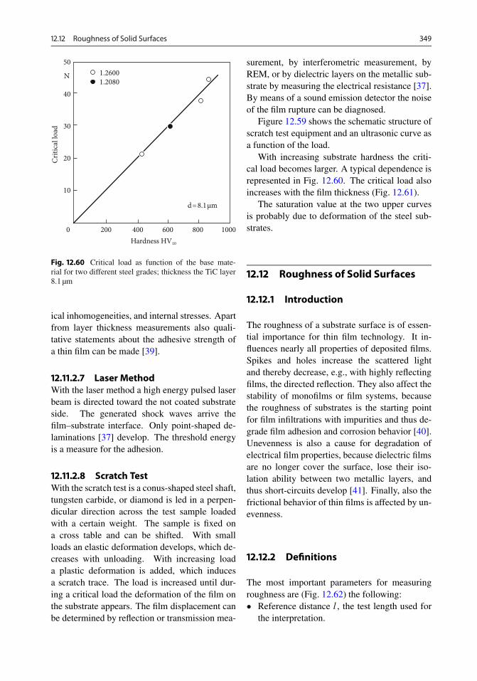
12.12 Roughness of Solid Surfaces 349
50
40
30
20
10
200 400 600 800 10000
N
Criti
cal l
oad
Hardness HV10
d=8.1μm
1.26001.2080
Fig. 12.60 Critical load as function of the base mate-rial for two different steel grades; thickness the TiC layer8.1 µm
ical inhomogeneities, and internal stresses. Apartfrom layer thickness measurements also quali-tative statements about the adhesive strength ofa thin film can be made [39].
12.11.2.7 Laser MethodWith the laser method a high energy pulsed laserbeam is directed toward the not coated substrateside. The generated shock waves arrive thefilm–substrate interface. Only point-shaped de-laminations [37] develop. The threshold energyis a measure for the adhesion.
12.11.2.8 Scratch TestWith the scratch test is a conus-shaped steel shaft,tungsten carbide, or diamond is led in a perpen-dicular direction across the test sample loadedwith a certain weight. The sample is fixed ona cross table and can be shifted. With smallloads an elastic deformation develops, which de-creases with unloading. With increasing loada plastic deformation is added, which inducesa scratch trace. The load is increased until dur-ing a critical load the deformation of the film onthe substrate appears. The film displacement canbe determined by reflection or transmission mea-
surement, by interferometric measurement, byREM, or by dielectric layers on the metallic sub-strate by measuring the electrical resistance [37].By means of a sound emission detector the noiseof the film rupture can be diagnosed.
Figure 12.59 shows the schematic structure ofscratch test equipment and an ultrasonic curve asa function of the load.
With increasing substrate hardness the criti-cal load becomes larger. A typical dependence isrepresented in Fig. 12.60. The critical load alsoincreases with the film thickness (Fig. 12.61).
The saturation value at the two upper curvesis probably due to deformation of the steel sub-strates.
12.12 Roughness of Solid Surfaces
12.12.1 Introduction
The roughness of a substrate surface is of essen-tial importance for thin film technology. It in-fluences nearly all properties of deposited films.Spikes and holes increase the scattered lightand thereby decrease, e.g., with highly reflectingfilms, the directed reflection. They also affect thestability of monofilms or film systems, becausethe roughness of substrates is the starting pointfor film infiltrations with impurities and thus de-grade film adhesion and corrosion behavior [40].Unevenness is also a cause for degradation ofelectrical film properties, because dielectric filmsare no longer cover the surface, lose their iso-lation ability between two metallic layers, andthus short-circuits develop [41]. Finally, also thefrictional behavior of thin films is affected by un-evenness.
12.12.2 Definitions
The most important parameters for measuringroughness are (Fig. 12.62) the following:� Reference distance l , the test length used for
the interpretation.

350 12 Measurements of Thin Layers After the Coating Process
Fig. 12.61 Critical loadas a function of the TiCfilm thickness for steelsubstrates of differenthardness
50
40
30
20
10
2 4 6 8 10 12 μm 160
N
Criti
cal l
oad
Layer thickness
890 HV10
810 HV10
430 HV10
� Reference profile, the profile, at which theshape deviations are referred.
� Mean profile, reference profile, which isshifted in such a way within the reference dis-tance that the sum of the enclosed of surfacepartAoi above and Aui below the mean profileis equal.
� Ground profile, reference profile, which isshifted so far perpendicularly to the geomet-rically ideal profile that it affects the furthestpoint of the actual profile T away from the ref-erence profile.
� Roughness Rt, distance of the ground profilefrom the reference profile.
� Smoothing depth Rp, middle distance of thereference profile from the actual profile.
a
b c d
X
H
eT
R p
hi Fui
Foi
hi
R t
f
Fig. 12.62 Situation of the reference profile to the actual profile. a Geometrically ideal profile, b actual profile, c pointof reference, d middle profile, e ground profile, f roughness profile distance l
� Average rough value Ra, arithmetic averagevalue of the absolute values of the distanceshi of the actual profile from the mean profile:
Ra D 1
l
xD1Z
xD0jhi j � dx : (12.116)
12.12.3 Measuring InstrumentsandMeasuringMethods
12.12.3.1 Mechanical Measurement(Stylus Method)
A method for roughness measurement is the me-chanical scanning of the surface. The vertical

12.13 Measuring of Film Thickness 351
15μm
1μm5μm radius
Fig. 12.63 Schema of a tip measurement with exemplarystatements of size
R
L/2
Fig. 12.64 Example of the deviation of a profile taken upwith the stylus method from actual geometry, L reductionof the profile distance
movement of a stylus is amplified electronically.Deviations from the ideal surface of the substrateor the applied film are recorded. Exact rough-ness measurements require particularly pointedtips with very small bearing pressures. The func-tion of the tip radius is shown in Fig. 12.63.
Figure 12.64 shows that at an edge profile themeasured width of a valley fails more narrowly,where it is larger than the curve radius of the tip.
The advantage of the stylus method is thatwith accordingly small curve radius of the tip ofthe scanning pin and with small scanning speedreal surface profiles are recorded. For exact mea-surement a REM must be used [42].
The main disadvantage is the surface contact.A slow measurement is the result. With soft ma-terials this can lead to a destruction of the surface.A further disadvantage is the linear scanning,which does not lead to good reproducibility ofthe measured values.
12.12.3.2 Roughness Measurementsby Microscope Interferometers
The microscope interferometer is based on theMichelson interferometer (contribution optics,temporal coherence function). With a shift ofthe sample, changes from the sample beam travelsome distance and from there the phase oppositethe reference beam also changes (Fig. 12.65). Ateach point of the interferogram the brightness of
the wave and thus the level of the surface on theappropriate place of the sample surface can becalculated.
The phase difference of all positions may notdistinguish more than one wavelength. Threewavelengths must be used to contain all neces-sary information, in order for us to be able todetermine for each point on the examined surfacethe phase difference between reference and sam-ple beam. From the calculated phase differenceswe can analyze the topography of the sample.Unevenness of less than 1 nm can still be dis-solved.
12.13 Measuring of Film Thickness
The methods for the measuring of optical thick-ness are treated in detail in the chapter on optics.In the following, only methods that are not basedon optical systems are described.
12.13.1 Film Thickness Determinationby Particle Emission
The methods presented in this chapter are usuallydesignated by users and equipment manufactur-ers as methods for measuring film thickness.However, with these not the film thickness ismeasured, but the mass allocation of a detectedsample. The transformation of a dimension intoanother one is usually possible without difficul-ties. With procedural errors, like strong oxygeninsertion into a metal film, the mass allocationremains nearly unchanged, the geometrical filmthickness can, however, be substantially larger.
12.13.1.1 Beta Backscattering MethodThe principle of the beta backscattering methodfor measuring the film thickness is shown inFig. 12.66.
A screen separates the measuring surface fromthe material to be measured. From the screencenter a beta sends emitters (electrons), whichcome from a nuclear disintegration, beta parti-cles (electrons). The electrons are partly elasti-

352 12 Measurements of Thin Layers After the Coating Process
Fig. 12.65 Principle of themicroscope interferometer
To the detector
Reference mirror
Laser
Sample
Fig. 12.66 Principleschema of ˇ backscat-tering thin film measuringequipment
Counting tube β-source
Backscattered electrons x
Layer thickness d
Substrate
cally backscattered on the sample. Some of thebackscattered electrons are collected by a detec-tor. With homogenous samples, the backscattercoefficient depends practically only on the ordi-nal number Z of the material. The backscattercoefficient is a measure for the film thickness.For conditions with constantly held backscattercoefficient, the counting rate is directly indi-cated from the reflected electrons. Figure 12.67shows the connection between measured stan-dardized counting rate and film thickness for goldon nickel.
The standardized counting rate is xn D .x �x0/=.xs � x0/, where x0 is the counting rate ofthe uncoated substrate, xs the counting rate of thesubstrate with saturation film thickness, and x thecounting rate of the sample with interesting filmthickness.
An important condition for the applicabilityof the beta backscattering method is that thebackscatter coefficients of the substrate mate-rial and the film material are sufficiently farapart. Only then does film thickness variationcause a clearly detectable change of the counting

12.14 Determination of Pinhole Densities 353
10
3
1
0.3
0.1
μm
Laye
r thi
ckne
ss d
0 0.2 0.4 0.6 0.8 1.0Standarized counting rate xn
Fig. 12.67 Dependence of the layer thickness on the stan-dardized counting rate with the example of gold on nickel
20
15
10
5
Ord
inal
num
ber d
iffer
ence
z S-z
0
0 20 40 60 80Ordinal number z0 of the base material
Fig. 12.68 Necessary ordinal number difference as func-tion of the ordinal number of the basic material
rate of backscattered electrons. The necessaryordinal number difference as function of the or-dinal number of the basic material is shown inFig. 12.68.
The beta backscattering method is problem-free with layers of metal on metal substrates.Complications can occur if substrate and/or filmmaterials from alloys, oxides, or composite ma-terials are present. Here it must be proven in
individual cases whether this measuring methodalso gives usable results for the available applica-tion [43].
12.13.1.2 Other Film Thickness MeasuringMethods
Further methods to measure film thickness are:� X-ray fluorescence method [44]� Measuring of film thickness with EDX� Measuring of film thickness by weighing.
12.14 Determination of PinholeDensities
Films generated by PVD (Physical Vapor Depo-sition) processes usually various defects. Someof these are due to the so-called pinholes, holesthat go through the film up to the substrate.
Pinholes can result from impurity particlesthat were on the substrate and were not removedby cleaning before coating. On the other hand,evacuation can whirl up impurity particles, whichare deposited on the substrate. A further sourceof pinholes are coatings on screens or coverplates, which peel off due to high internal stressesor thermal expansion.
A further cause for pinholes is the coatingprocess itself. Thus, with incorrect processing,vaporization can lead to splashes of metal burn-ing holes into the foil. In reactive sputteringprocesses arc generation can be a problem; tem-porary discharges between carriers and substratecan lead to punctual defects. Flaking of screenscan be minimized, as the screens are held at con-stant temperature during all phases of the coatingprocess. Another way is to adapt the screen mate-rial regarding its thermal expansion behavior onthe growing layers.
Pinhole densities on somewhat optically re-flecting samples can be determined quickly withlaser scanning techniques [45]. A laser beamscans over the sample; its reflected light is mea-sured directly by a detector. If the laser beamencounters a punctual defect, the light is scat-tered, and the detector registers a decrease of thedirectly reflecting intensity.

354 12 Measurements of Thin Layers After the Coating Process
The pinholes in the insulator foils are deter-mined by measuring the capacitance by puttingthe foil between two capacitor plates. The capac-itance is a measure of the pinhole density.
References
1. Franz R, Wiedemann G (1853) Über die Wärme-Leitungsfähigkeit der Metalle. Annalen der Physikund Chemie 8(Bd. LXXXXIX):1853
2. Dua AK, Agarwala RP (1971) Thermal conductiv-ity of thin films of alkali metals. Thin Solid Films10:137–139
3. Patrick WJ (1966) Measurement of resistivity andmobility in silicon epitaxial layers on a control wafer.Solid-State Electronics 9(3):203–211
4. Maissel LI, Glang R (1970) Chapter 13. In: MaisselLI, Glang R (eds) Handbook of Thin Film Technol-ogy. McGraw-Hill, New York
5. Ishikawa Y, Miura N (1991) Physics and EngineeringApplication of Magnetism. Springer, Berlin
6. Stoner EC, Wohlfahrth EP (1991) A mechanism ofmagnetic hysteresis in heterogeneous alloys. IEEETrans on Magnetic 27:4475–3518
7. Foner S (1975) Further improvements in vibrat-ing sample magnetometer sensitivity. Rev Sci Inst46:1425–1435
8. Flanders PJ (1988) An alternating-gradient magne-tometer. J Appl Phys 63:3940–3945
9. Solymar L (1972) Superconductive Tunneling andApplication. Chapman and Hall, London
10. Hornauer H, Atommono TM, Röll K (1990) A Kerrmagnetometer using Faraday modulation technique. JMagn Magnetic Materials 83:551–552
11. Rohrmann H, Hoffmann H (1989) High-resolutionKerr observation of magnetic domains. Thin SolidFilms 175:273–279
12. Hamrle J et al (2007) Huge quadratic magneto-opticalKerr effect and magnetization reversal in the Co2FeSicompound. J Phys D: Appl Phys 40:1563
13. Wyszecki G (1978) Colometry. In: Driscoll WG,Vaughan W (eds) Handbook of Optics. McGraw-Hill,New York
14. Schrift Nr. 537 316/8.88 der Minolta GmbH, Ahrens-burg, Germany
15. Durrant BG (1984) Barrier & Sealing – The prospectsfor metalized PP, Paper, Film & Foil Converter, pp61[12-11]
16. Krauss WM (1984) Objective/subjective views ofmetalized food packaging. Paper, Films & Converter55:58–60
17. Born M, Wolf E (2003) Principles of optics, 7th edn.Cambridge University Press
18. MacAdam DL (1985) Color measurement, 2nd edn.Springer
19. Pedrotti FL, Pedrotti LS (1993) Introduction to Op-tics, 2nd edn. Prentice Hall
20. Azzam RMA, Bashara NM (1992) Ellipsometry andpolarized light. North-Holland
21. Lawes G (1987) Scanning electron microscopy and x-ray microanalysis. Wiley
22. Reimer L (1985) Scanning electron microscopy:physics of image formation and microanalysis.Springer
23. “Handbook of microscopy” VCH, 1997
24. Saleh BEA, Teich MC (2007) Fundamentals of Pho-tonics. Wiley
25. Tu KN, Rosenberg R (1988) Analytical techniques forthin films Treatise on Materials Science and Technol-ogy, vol. 27. Academic Press, Inc., Boston
26. Windischmann H (1991) Intrinsic stress in sputteredthin films. J Vac Sci Technol A 9(4):2431–2436
27. Klokholm E (1968) Intrinsic stress in evaporated. JVac Sci Technol 6:138–140
28. Orent T (1991) Stress modification in sputtered zincsulfide and zinc oxysulfide thin films. J Vac Sci Tech-nol A 9(4):2447–2452
29. Rossnagel SM, Glistrap P, Rujkorakarn R (1982)Stress measurement in thin films by geometrical op-tics. J Vac Sci Technol 21(4):1045–1046
30. Klokholm E (1969) An apparatus for measuring stressin thin films. The. Review of Scientific Instruments40:1054–1058
31. Nix WD, Mehl RF (1989) Mechanical Properties ofThin Films. Metallurgical Transaction A 20:2217–2244
32. Bangert H, Kamintschek A et al (1986) Ultramicro-hardness Measurement on Aluminum Films Evap-orated under Various Conditions. Thin Solid Films137:193–198
33. ISO 409/1: Metallic materials – Hardness test –Tables of Vickers hardness values for use in testsmade on flat surfaces – Part 1: HV 5 to HV 100.Ed.: International Organization for Standardization,409/1-1982 (E).
34. ISO 4516: Metallic and related coatings – Vickers andKnoop microhardness tests – Ed.: International Orga-nization for Standardization, 4516-1980 (E).
35. Fischer-Cripps AC (2004) Nanoindentation. Springer
36. Mittal KL (1975) Surface chemical citeria for maxi-mum adhesion and their verification against the exper-imentally measured adhesive strength values. In: LeeLH (ed) Adhesion Science and Technology, 9th edn.Plenum Publishing Corporation, New York, pp 129–168

12.14 References 355
37. Valli J (1986) A review of adhesion test methods forthin hard coatings. J Vac Sci Technol A 4(6):3007–3014
38. Ganz S, Krämer KF (1990) Zerstörungsfreie Unter-suchung mit hochauflösender Akustomikroskopie vin10 MHz bis 2 GHz. Kunststoffe 80:602–606
39. Hoppe M, Bereiter-Hahn J (1985) Applications ofScanning Acoustic Microscopy – Survey and NewAspects. IEEE Transactions on Sonics and Ultrason-ics SU-32(2):289–301
40. Kienel G (1992) Plasma-assisted vacuum coating pro-cesses. Int J of Modern Phys B 6:1–24
41. Marton D, Fine J (1990) Sputtering Induced SurfaceRoughness of Metallic Thin Films. Thin Solid Films185:79–90
42. Bennett JM (1985) Comparison of instruments formeasuring step heights and surface profiles. Reprintfrom Applied Optics 24:3766–3772
43. Ott A (1974) Neue Erkenntnisse bei derradiometrisch-elektronischen Messung von Schicht-dicken. Chemie Ingenieur Technik 46(19):805–811
44. Rößiger V, Thomas HJ (1990) Quantitative XRFAnalyisis of Surface Layers: Procedure of the De-termination of Thickness and Composition. X-RaySpectrometry 19:211
45. Licari JJ, Enlow LR (1988) Hybrid Microciruit Tech-nology Handbook. Noyes Publications, Park Ridge

13Nanoparticle FilmsH. R. Khan
This chapter gives a short introduction to nano-materials and a description of the synthesis ofnanoparticle films. It further describes in de-tail two nanoparticle film systems, i.e., magneticnanocomposites in which magnetic nanoparti-cles are randomly distributed and nanostructuredmagnetic nanocomposites in which magneticnanoparticles are embedded in a structured insu-lating matrix, and nanoparticle ZnO-based films.
13.1 Introduction to Nanomaterials
In 1959 at the annual meeting of the Ameri-can Physical Society, [1] in his historical lecturesaid “There is plenty of room at the bottom”and opened a new field of solid state physicsand the discussion of synthesizing materials ona smaller scale. This was the beginning of thefields of nanotechnology and nanoscience. Inthe 1980s two major developments, the birth ofcluster science and the invention of scanning tun-nel microscopy (STM by Rohrer and Binning)took place. This technique makes it possible toobserve very small material structures down toindividual atoms. The atomic force microscopy(ATM) was invented about 5 years after the in-vention of STM. These developments contributedto the discoveries of many nanomaterials suchas fullerenes, carbon nanotubes, nanocrystallinesemiconductors, and magnetic nanocrystals andcomposites.
Particles with sizes range between 1 and100 nm are defined as as nanomaterials. These
nanomaterials may have different geometricalshapes such as globular, plate-like, rod-like, ormore complex geometries. Spherical particlessmaller than 10 nm are defined as clusters, andthe number of atoms in a cluster increases withthe diameter of the cluster. As the number ofatoms in a cluster increases, there is a criti-cal size of the cluster above which a particu-lar bond geometry that is characteristic of thebulk solid is energetically preferred, such thatstructure switches to that of bulk. Materialsbelow a critical dimension of 100 nm exhibitvery different physical and chemical propertiescompared to their bulk counterparts. Moreoverbulk materials have constant physical proper-ties regardless of their size, but with nanodi-mensions this is often not the case. Just tomention a few, the size-dependent properties arequantum confinement in semiconductors parti-cles, surface plasmon resonance in some metalparticles, and superparamagnetism in magneticparticles.
Nanoparticles have a very high surface areato volume ratio. This provides a tremendousdriving force for diffusion at elevated tempera-tures. The dramatic changes in physical prop-erties of the materials such as melting point,optical properties (such as color due to changesof the optical band gap and wavelength of the op-tical transition), mechanical hardness, magneticproperties (such as coercivity, permeability, sat-uration magnetization, magnetic ordering) andchemical properties (such as ionization potential,catalytic activity, or selectivity) take place after
357© Springer-Verlag Berlin Heidelberg 2015H. Frey, H. R. Khan, Handbook of Thin-Film Technology, DOI 10.1007/978-3-642-05430-3_13

358 13 Nanoparticle Films
the transition from the bulk to nanoparticle stateof a material.
Nanoparticle films are thermodynamically un-stable compared to macroscopic films of largergrain sizes. The direct characterization of thenanoparticle size and shape as well the strain ina nanoparticle film is important after the syn-thesis of nanoparticle films. This can be doneby using high resolution electron microscopy(HTM) or scanning electron microscopy (SEM).These methods are limited because they providemeasurements on a very small localized surfacearea and only provide data of a relatively smallnumber of average grain sizes and shapes. Inaddition to microscopic techniques, a more con-ventional method that can be used is the x-raydiffraction technique. This technique is basedon the analysis of the line widths of the x-rayBragg peaks of the (�–2�) x-ray diffractograms.P. Scherrer [2, 3] correlated the particle size ina film or in a powder to the full width at half ofthe maximum of the x-ray diffraction line:
�� D k�=L cos� :
Here � is the x-ray wavelength, k the Scherrerconstant (which is 0.9 for the spherical particles),2� is the scattering angle in the (�–2�) x-ray diffractogram, and L is the volume-weightedaverage column length and is equal to 0:75D,where D is the grain diameter of the sphericalparticle. This way of determining the parti-cle size is applicable to smaller nanograin sizes(larger broadening of the diffraction peaks) andin the absence of microstrain.
The x-ray diffraction technique also allows thedetermination of the microstrain in the nanopar-ticles (4). Microstrain in nanoparticles describesthe relative mean square deviation of the lat-tice spacing from its mean value and depends onthe grain size. This shows that there is a straingradient in a nanoparticle, but x-ray diffractiongives a homogenous volume averaged value ofthe microstrain. The nanoparticle size D and themicrostrain " are related by the equation:
�� cos� D �=D C 4" sin� ;
where " and D are determined from the�� cos� versus sin� graphic plot. It shouldbe noted that not only the x-ray diffraction linewidth but also the shape of the line changes withthe nanoparticle size. Smaller size nanoparticleshave higher microstrain. The lattice contractionof the smaller particles is a result of the co-ordination of the surface atoms and extra pressureis exerted due to the surface stress.
13.2 Synthesis of Nanoparticle Films
The most commonly used methods to depositnanoparticle films are physical methods such aselectron beam deposition (EBD), pulsed laserablation or deposition (PLD), and ion beam de-position (IBD) or ion-assisted beam deposition(IABD). Chemical methods such as chemical va-por deposition (CVD), sol–gel, and electrochem-ical deposition techniques are also used to depositnanoparticle films. These deposition techniquesare described in detail in various chapters of thebook (Chapters 6, 7, 8, 9).
First to compare the merits and demerits ofa physical and a chemical method e.g., the CVDand PLD techniques, the synthesis of nanoparti-cle diamond films is described in short as an ex-ample. The electron beam evaporation techniqueto deposit the films of magnetic nanocompos-ites, ordered films of ferromagnetic nanoparticlefilms using electrochemical technique, and theion beam deposition technique to deposit thenanoparticles films of ZnO are described below.
13.2.1 Diamond Films Deposited byChemical Vapor Deposition(CVD) and Pulsed Laser Ablation(PLD) Techniques
CVD is a chemical process to deposit films ofmaterials having polycrystalline, nanocrystalline,or amorphous microstructures. There exist vari-ations of the CVD technique that differ in thechemical reactions and are classified depend-ing on the operating pressure, operating plasma,and the precursor used. Operating pressure-

13.2 Synthesis of Nanoparticle Films 359
based CVDs are subclassified as atmosphericpressure (APCVD), low pressure (LPCVD) andultra high vacuum (UHCVD) CVDs. LPCVDworks at reduced pressures (mTorr) to reduce theunwanted gas impurities in the deposited film.UHCVD works at low pressures, typically below10�8 Torr. MOCVD is based on using metalor-ganic precursors. Microwave plasma enhanced(MEPCVD) is a technique in which the chem-ical reaction on the substrate is enhanced bythe plasma and the deposition temperature canbe reduced substantially. The CVD techniqueis widely used to deposit the nanoparticle filmsof those materials that are available as gases orvolatile liquids.
The morphology of the nanoparticle film de-pends on the reactant gases, their mixing ratio,and the substrate temperature.
A typical example is the nanocrystalline dia-mond film deposited using CVD and acetyleneand hydrogen as chemical precursors. At lowpartial pressures, highly crystalline primary sp3-bonded diamond film is obtained. As the par-tial pressure increases, a more disordered filmis formed, which contains the disordered struc-ture graphite in which nanocrystalline diamondclusters are embedded. By adjusting the partialpressure, a high quality nanocrystalline diamondfilm mostly sp3 bonding is obtained, which has asmoother surface and improved electronic prop-erties. Nanocrystalline diamond films can begrown from methane or fullerene precursors withor without the addition of argon or molecular hy-drogen as carrier gases. The films contain mostlysp3 bonding with 1 to 2 % sp2 bonding residingat the grain boundaries.
On the other hand, in the PLD technique,a solid target is irradiated with a laser beam andthe material ablated from the target is depositedas a film on a substrate. In this method, no spe-cial gaseous precursors as in the case of the CVDtechnique are required. Diamond films can be de-posited using a graphite target. The laser plasmadischarge containing C3C and C4C is acceleratedand deposited onto a cold substrate or at roomtemperature. Hard dense nodules of diamond of10–50 nm in size are formed. Coatings of 2 to
5 µm thickness can be deposited on a variety ofsubstrates, such as steel, whereas poor adhesionand chemical reactions occur in CVD deposition.
Diamond is chemically inert and is transpar-ent from UV to the IR spectrum. This propertycan be used to deposit protective coatings ontransparent substrates. The main problem isthe surface roughness of diamond films, whichcauses attenuation and scattering of the inci-dent light. Nanocrystalline diamond films aremuch smoother and show enormous potential indiamond optics. Nanocrystalline films have a sur-face roughness of about 8–40 nm in a 1 um thickfilm. With this surface roughness, there is a sig-nificant reduction of visible light transmission,but there is no reduction in the transmission of theIR spectrum. Moreover, the optical transparencyis about 85 % for radiation of wavelengths above700 nm.
13.2.2 Magnetic Nanocomposites
Magnetic nanoparticles (particles smaller than100 nm in size) that are randomly or orderly dis-tributed in a nonmagnetic conducting or insulat-ing matrix are defined as magnetic nanocompos-ites. The matrix may be metallic, semimetallic,semiconducting, or insulating. These magneticnanocomposites exhibit magnetic properties thatare very different from the bulk. In the lastyears, much effort has been made to synthesizeand understand the magnetic and magnetoresis-tive properties of these composites for practicalapplications. A multilayer system based on thealternate layers of magnetic and nonmagnetic(metallic or insulating) films of nanometer thick-ness shows enhanced magnetoresistance and hasbeen called giant magnetoresistance (GMR) afterits discovery by Grünberg et al. or tunnel mag-netoresistance (TMR). Magnetic nanocompositesmay be pictured as three-dimensional multilayersystems. There is a similarity between themagnetic multilayer and magnetic nanocompos-ite systems. Magnetic multilayers and magneticnanocomposites are useful in applications suchas magnetic information storage media, magnetic

360 13 Nanoparticle Films
sensors and in high frequency devices. Presentcomputers are already equipped with readingheads based on the nanodimensional magneticmultilayers. These magnetic multilayers may besubstituted by magnetic nanocomposites, whichare much easier to prepare in an economical way.
Much effort has been made to understand theinfluence of particle size on magnetic parameterssuch as remanence Mr, coercivity Hc, and sat-uration magnetization Ms. These are importantmagnetic parameters from the application pointof view. They change drastically with the dimen-sion of the magnetic particles. A typical exampleis the assembly of iron nanoparticles. A 20 nmFe particle produced by evaporation exhibits co-ercivity up to two orders of magnitude higherthan bulk Fe, and the saturation magnetizationvaries between 20–90 % of the bulk, dependingon the iron particle size. The maximum coer-civity of a ferromagnetic material is observedwhen the particle size reaches the critical sizeof a single domain structure. The coercivities ofnanoparticles of Fe, Co, and Ni agree very wellwith the theoretically calculated values based onthe single domain structure. Frenkel and Dorf-man predicted that magnetic particles consistingof single domains can exist, and Kittel estimatedthat a transformation from multidomain to a sin-gle domain occurs at a particle size of about15 nm in a common ferromagnetic element. Theremanence Mr of a magnetic material arises be-cause the magnetic moments of some parts ofthe sample have energy barriers that they can-not reverse without the assistance of an externalmagnetic field or thermal energy. Remanenceis related to the intrinsic properties of the mate-rial. If the concentration of magnetic particles ina composite varies, then magnetic interaction isaffected due to the variation of the interparticlespacings. Therefore, the remanence curves area guide to the semi-quantitative assessments ofthe magnetic interactions. The particle size ofa magnetic component in a composite may bevaried down to a single domain structure, andthe composite may show a behavior ranging fromferromagnetic to superparamagnetic and variousdegrees of coercivities. The magnetic componentin a composite may be a single element such as
Fe, Co, or Ni or alloys such as FeNi, CoFe, etc.([5–9]).
After the discovery of GMR [10] in mag-netic and nonmagnetic multilayers, as mentionedearlier, nanocomposites based on the disordereddistribution of the magnetic nanoparticles dis-tributed in a metallic matrix such as Ag, Cu, etc.,also showed a GMR effect [11]. The origin ofGMR in these multilayers and composites is fromthe spin-dependent scattering of the conductionelectrons on the magnetic nanoparticles and issize dependent.
If the matrix is insulating, such as Al2O3
or SiO2, then after a threshold concentration ofthe magnetic nanoparticles, the composite trans-forms from the insulating to the conducting state.This transformation is caused by the tunnelingof the electrons through the insulating barrierseparating the two magnetic nanoparticles. Themagnetoresistance of these nanocomposites iscalled tunnel magnetoresistance (TMR) [12, 13]TMR is very sensitive to the magnetic field ap-plied and may be used to make magnetic fieldsensing devices. Magnetic nanocomposites maybe synthesized by PVD techniques, as mentionedearlier. Each technique has its own merits anddemerits.
A series of magnetic nanocomposite filmssuch as Al–Co, AlCo–O, Co–Cu, Co–Ag, Fe–Ag, FeNi–Ag, FeRu, and CoFe–Al2O3 have beeninvestigated [14–23]. Two magnetic nanocom-posite systems are described here: one disordered(magnetic nanoparticles randomly distributed)and the other one ordered (magnetic nanoparti-cles are arranged orderly) in an insulating matrixsuch as Al2O3.
13.2.3 Disordered MagneticNanocomposites.Co50Fe50/x.Al2O3/100�x
Nanocomposite films composed of nanometer-sized magnetic particles distributed in an insulat-ing matrix and exhibiting the TMR effect havereceived much attention, not only for their po-tential applications but also for their value infundamental understanding. Composite films are

13.2 Synthesis of Nanoparticle Films 361
traditional model systems for critical percolationbehavior studies and the investigation of basicmagnetic and transport properties of granular fer-romagnets. There is a wealth of information inthe literature on this topic [24–32].
In most cases, the films are prepared by mag-netron sputtering using composite targets [24–26,30], tandem deposition [31], or reactive sputter-ing [32]; other techniques are rarely used. Alsothe preparation and characterization of SiO2-based films are often reported [24–26, 30, 31],while data on Al2O3-based films are lacking.Recently, a number of publications on the mag-netic and transport properties of Al-oxide-basedfilms prepared by reactive sputtering [32] or ionbeam deposition [33, 34] appeared. Althoughthe microstructure, transport, and optical proper-ties of electron beam evaporated films have beenstudied [29], there is a lack of work on magneto-transport for this type of film.
The analysis of microstructure, concentrationdependence of magnetoresistance, and correla-tion between transport and magnetic propertiesfor electron beam evaporated composite filmsconsisting of magnetic nanoparticles of Co50Fe50
in insulating matrix of Al2O3 are described here.Thin .Co50Fe50/x.Al2O3/100�x composite
films with a magnetic volume fraction of 0:07 <x < 0:52 and a thickness of about 400 nm aredeposited on glass substrates at room tempera-ture in vacuum of 10�4 Pa using the dual electronbeam deposition technique [35]. The thicknessand composition of the films is determined usingoptical measurements of the thickness profilesof the reference films deposited from individualtargets and using energy dispersive analysis ofx-rays (EDAX). The bulk densities of Co50Fe50
and Al2O3 are used in the calculations. Thecrystalline structure of the films is investigatedby the (#–2#) Bragg–Brentano x-ray diffrac-tion (XRD) technique using CuK˛ radiation andtransmission electron microscopy (TEM). Thesamples for TEM studies are prepared by polish-ing off the original samples substrate with furtherion milling of the film in Ar plasma. The elec-trical resistance (�) and magnetoresistance (MR)are measured by a four-point technique in thetemperature range of 5–300 K using the quantum
3nm
a
b
2
1
3
54
2
31
Fig. 13.1 High resolution transmission electron micro-graph (a) and an electron diffraction pattern (b) of a de-posited film .Co50Fe50/0:16–.Al2O3/0:84
design physical property measurement system.MR is measured in magnetic fields (H) up to 5Tin current-in-plane configuration and differentgeometries:1. with H in the film plane and parallel current
(I; L – longitudinal geometry).2. H in the film plane but perpendicular to I (T –
transverse geometry).The MR values are determined as MR D
Œ�.H/ � �.0/�=�.0/, where �.0/ and �.H/ arethe resistance of the film in zero and in an appliedmagnetic field, respectively. Room temperature(RT) magnetic hysteresis loops are measured inthe fields up to 5T using the quantum designSQUID magnetometer withH parallel to the filmplane.
The lattice structure as analyzed by XRDdemonstrated that the films are x-ray amorphous.X-ray diffractograms showed only a broad peakthat corresponded to h110i body centered cubic(bcc) Co50Fe50. A high resolution transmissionelectron micrograph and the associated electrondiffraction pattern of a deposited film with x D0:16 are shown in Fig. 13.1.
Two types of crystalline particles embeddedin the amorphous matrix can be observed. Thefirst is spherical crystalline particles with an av-

362 13 Nanoparticle Films
erage size of about 2 nm (Fig. 13.1a, markedas 1). The second is small crystalline regionswith the size of a few lattice periods (Fig. 13.1a,marked as 2 and 3). The size of the latter crys-talline regions is about 1 nm. The formation ofsuch a structure is typical for composite filmsand is caused by the low migration rate of oxideclusters that prevent coalescence and recrystal-lization of the metal phase [26, 27]. Analysisof the diffraction rings allows us to concludethat the film consists of hexagonal close packed(hcp) Al2O3 and bcc Co50Fe50 particles. Thefirst line can be considered as h110i hcp Al2O3.The second one can be attributed to superposi-tion of h110i bcc Co50Fe50 and h113i hcp Al2O3.The third line is h211i hcp Al2O3. The fourthand fifth lines are the result of the superposi-tion of h200i bcc Co50Fe50Ch300i hcp Al2O3 andh211i bcc Co50Fe50 C h2010i hcp Al2O3, respec-tively.
Additional structural information can be ob-tained and the evolution of the magnetic structurewith concentration x can be conveniently studiedby measuring the magnetic properties. Mag-netization measurements demonstrate that themagnetic phase of the films changes from su-perparamagnetic to ferromagnetic with increas-ing x. The RT magnetization curves are shownin Fig. 13.2 for films with x D 0:09, 0.12, 0.16,0.24, and 0.50.
No visible hysteresis is found for films withx < 0:16. The magnetic phase in the filmsof these compositions should be considered atRT as an ensemble of small noninteractive mag-netic particles in superparamagnetic state [25].With increasing x a gradual transition from thesuperparamagnetic to the ferromagnetic state oc-curs. For x > xc, the shape of the hysteresisloop shows contributions of the ferromagneticand the superparamagnetic phases. For x D0:50, a narrow loop width is observed and themagnetization is almost saturated in fields higherthan 1000 Oe. However, the residual magneti-zation (remanence) is lower than 0:15Ms (Ms
is the saturation magnetization). This type ofmagnetic state transition and the shape of themagnetization loops are typical for compositefilms [25, 31] but seem to be different from
–40k –20k 0 20k 40k–2000
–1000
0
1000
2000
–500 0 500
–0,5
0,0
0,5
x=0.24
x=0.50x=0.16
x=0.12x=0.09
M (e
mu/
cm3 C
oFe)
H (Oe)
x=0.16x=0.5
x=0.24M/Ms
Fig. 13.2 Magnetic hysteresis loops with in plane mag-netic field for .Co50Fe50/x-.Al2O3/100�x compositefilms of different compositions at T D 300K
those described recently for discontinuous metal-insulator multilayers [34], where a sharp onset offerromagnetism was observed. Probably this dif-ference is determined by the microstructure of thefilms and the dissimilarity in the topology of theferromagnetic phase.
An estimation of the magnetic cluster sizeswas made according to the model proposed [24]using a bimodal cluster size distribution and withthe assumption of spherical magnetic clusters. Inthe model fitting, the following equation is used:
M DMs�W1L.V1H=kBT /
C .1 �W1/L.V2H=kBT /�; (13.1)
where L is the Langevin function, V1 and V2 arethe two volumes of the particles, kB is the Boltz-mann constant, T is the temperature, and W1 isthe volume fraction of the particles with the vol-ume V1.
The spontaneous magnetization Ms � 1840
emu=cm3 was determined from measurements ofthe CoFe reference film. This value is within 5 %of the bulk value for Co50Fe49:7 permendur al-loy. For film of volume fraction x D 0:09 thebest fit of the experimental curves gave radii of

13.2 Synthesis of Nanoparticle Films 363
r1 � 1:2 nm (W1 � 0:14) and r2 � 0:4 nm(1 � W1 � 0:86). For films with x D 0:16 wehad r1 � 1:8 nm (W1 � 0:24) and r2 � 0:5 nm(1 �W1 � 0:76). The estimated cluster sizes areconsistent with the values of TEM observations.It is to be pointed out that the derived size ofthe particles does not change significantly with x,while the volume fraction, 1�W1, of the smallerparticles decreases. This should be attributed tothe coalescence processes that take place withchanging x. The progressive coalescence is alsoreflected in the concentration dependence of theresistance. The analysis of � vs. x dependence isused to determine the percolation threshold andis important for the study of the topology of thesegregated conducting phase. The general ruleof this dependence is the dramatic decrease ofthe resistance in the vicinity of the percolationthreshold [24–30]. For the series of films studied,the percolation threshold was determined fromthe � vs. x curve using the general effective me-dia equation [28]:
.1 � x/.�1=tm � �1=th /��1=tm C A�1=th
�
C x��1=tm � �1=tl
�
��1=tm C A�1=tl
� D 0 ; (13.2)
where �h, �l, and �m are the resistivities of theinsulator phase, the metal phase, and the wholefilm, respectively; x is the volume fraction of themetal phase, and t is an exponent. Also, A D.1 � xc/=xc, where xc is the percolation volumefraction of the metal phase.
The percolation parameters are determined asxc � 0:17 and t � 2:3; the parameters �l
and �h are estimated to be � 100 µ� cm and� 150� cm, respectively (Fig. 13.3a). Thevalue of �l is comparable to a pure CoFe filmdeposited under the same conditions for thick-ness calibration. The resistance of a referencefilm with polycrystalline structure is measuredto be 50 µ� cm. The enhanced �l value can beattributed to the nanoscale size and interface ef-fects [26, 27]. The low value of �h is caused by
disorders in the composite film structure as wellas partial alloying of Al2O3 with Co and Fe dur-ing film deposition [30].
The value of xc � 0:17 agrees well withthe theoretical prediction for a three-dimensionalsystem consisting of uniformly spherical parti-cles (xc D 0:16˙ 0:02) [28]. The derived valueof t is somewhat higher than the universal valuetun � 1:9 but is within the range 1:5 < t < 4 pre-dicted by the tunneling percolation model [36]. Ithas been shown both experimentally and theoret-ically that values of the percolation parametersare sensitive to the topology of the conductingphase, i.e., dimensionality, particle size distri-bution, tendency to form specific (columnar orlayered) structures. In continuous granular com-posites with variable particle size distributionthese parameters become nonuniversal and canvary in a wide range. They should be determinedfor each given case of the percolation structure.
It is to be pointed out that the percolationthreshold should not be mixed with the pointwhere the transition from metallic to insulatorconductance takes place. It is known [26, 29] thattransport in composites can be described usingthree different regimes of conductance – metallic,transition, and insulator. The electrical transportin metallic regime is due to conduction along themetal phase and is determined by electron scat-tering against grain boundaries, impurities, andphonons. This regime is observed for the compo-sition above xc when the film consists of insulatorinclusions in the metallic matrix. In the insulatorregime the conductance is governed by thermallyactivated tunneling between separated metal par-ticles. Such a conductance mechanism is typicalfor films of compositions below xc. In the tran-sition regime the conductance is due to a mixtureof metallic conductance along the percolationcluster and tunneling along the chain of isolatedparticles. The transition from metal to the insula-tor regime of conductance is usually determinedat the point where the temperature coefficient ofresistance (TCR) is equal to zero. This conditionshould be fulfilled at x and T where the contribu-tions from tunneling and percolation conductionare equal. In a disordered nanoscale cermet struc-ture the composition at which transition from

364 13 Nanoparticle Films
0.0 0.2 0.4 0.6 0.8 1.00
2
4
6
8
10T-geometry
H=1kOe
H=5kOe
H=10kOe
H=20kOe
H=50kOe
xc
Abs.
MR
(%)
Co50Fe50 vol. fraction
10–4
10–3
10–2
10–1
100
101
102
xc
ρ (Ω
cm)
experiment Equation (2)
ρh~150Ωcm
ρl~100μΩcmxc~0.17
t~2.3
a
b
Fig. 13.3 The dependence of electrical resistance (a)and magnetoresistance (b) for .Co50Fe50/x–.Al2O3/1�x
composite films as a function of composition
metal to insulator conductance takes place can bedifferent from the percolation threshold, althoughfor films with larger metallic particles the differ-ence can be small.
The percolation threshold for electron beamdeposited Cox–.Al2O3/100�x films is determinedfrom the � vs. x curve to be � 0:25, whileTCR at RT changes sign at x � 0:7. Contrarilyfor SiO2 – based magnetron sputtered films [24–26, 30, 31] the sign change of the TCR and adramatic increase of the film resistance both oc-cur within a narrow range of 0:4 < x < 0:65.This fact points to the important influence ofmicrostructure, type of insulator matrix, and de-position technique on the properties of the films.
0.1 0.2 0.310–2
10–1
100
101
102
103
104
x=0.09 x=0.12 x=0.16 x=0.24
ρ (Ω
cm)
1/T0.5 (K–0.5)
Fig. 13.4 Temperature dependence of resistance for.Co50Fe50/x–.Al2O3/1�x granular films. Solid lines rep-resent results of the experimental data fitting using theln.�/ � .Ec=T /
0:5 model with Ec D 0:104 eV, 0.05 eVand 0.015 eV for x D 0:09, 0.12, and 0.16, respectively
Using the Al2O3 matrix and the electron beamevaporation technique one can produce films withmetallic particles of 2–3 nm in diameter [29],while the films with the SiO2 matrix prepared bymagnetron sputtering are characterized by par-ticles of sizes 4–5 nm [25, 30, 31]. However,it is found that in all the cases the TCR at RTchanges sign for � � 10�2–10�3 � cm, whichcorresponds to the minimum conduction of themetal phase [26, 29]. For our films with x <
0:16 negative TCR and an exponential law R �exp.2.Ec=kBT /
0:5/ indicating tunneling type ofconductance is observed (Fig. 13.4).
Here Ec is an activation energy necessary tocreate a pair of charged particles during a ther-mally activated and/or bias assisted tunnelingprocess in a system with distribution of parti-cle sizes and interparticle distances [26]. Thevalue of Ec decreases with x due to an increas-ing number and size of metallic particles anddecreasing distances between them. For x >
0:16, the conductance still has activation charac-teristics but the temperature dependence cannotbe described by using the above-mentioned law.Negative TCR suggests nonmetallic conductiv-

13.2 Synthesis of Nanoparticle Films 365
ity such as semiconductor-like or amorphous-likeactivity [24, 27]. The TCR at RT becomes pos-itive for x > 0:35, while it is still negative fortemperatures below 270 K. Metal conductance ina wide temperature range was observed only forx > 45. Thus in our case, the transition tometallic conductance takes place at similar � val-ues (Fig. 13.3a). However, the value of xc andthe composition of the transition to the metallicregime of conductance are lower than reportedearlier for Al2O3-based films.
The correlation between � and MR as a func-tion of x can be seen in Figs. 13.3 and 13.5.
For x < 0:16, the TMR effect increaseswith x and the applied field. The dependen-cies of TMR vs. H coincide for transverse Tand longitudinal L geometries in this composi-tion range, indicating that the system is isotropic(e.g., Fig. 13.5, x D 0:09). Moreover, for com-positions x < xc no hysteresis behavior in lowfields and no saturation of TMR in fields up to50 kOe were observed. These data are in goodagreement with the magnetization measurementsand confirm that the system at RT consists ofsmall superparamagnetic granules.
A maximum isotropic TMR value of 10 % ina magnetic field of 50 kOe and at RT is observed.It is to be noted that the maximum of the TMRvs. H curve is shifted towards lower concentra-tion with increasing magnetic field. At the sametime, the saturation of TMR is more pronouncedfor films with a composition close to xc. Theseeffects are similar to the recently published dataon TMR in Co80Fe20=Al2O3 discontinuous mul-tilayers [34]. It is shown there that the highestvalue of TMR in granular systems should be ob-served in the case of superparamagnetic particleswith totally uncorrelated moments. Such condi-tions will be fulfilled for values of x sufficientlylower than xc. With an approaching percola-tion threshold a transition of the magnetic stateof the films occurs, i.e., magnetic moments ofthe clusters become correlated [31, 34]. Thedifferences for the TMR response in L and Tgeometries in the lower fields in the vicinityof xc (e.g. x D 0:12, 0.16) can also be at-tributed to formation of long chains of coalescedclusters with strong shape anisotropy. The mag-
–40k –20k 0 20k 40k–0.4
–0.3
–0.2
–0.1
0.0
–8
–6
–4
–2
0
–8
–6
–4
–2
0
–8
–6
–4
–2
0
0 1k 2k–0.10
–0.05
0.00
0.05
0 1k 2k–3–2–1
0
0 1k 2k
–2
0
0 1k 2k–1.0
–0.5
0.0
x=0.50
H (Oe)
x=0.16
x=0.12
MR
(%)
x=0.09
Fig. 13.5 Dependence of magnetoresistance vs. appliedmagnetic field for .Co50Fe50/x–.Al2O3/1�x compositefilms in L.ı/ and T .�/ geometries

366 13 Nanoparticle Films
netic moments of these chains can be correlateddue to dipole–dipole or in-plane inelastic interac-tions [31, 37, 38].
Such correlations can enhance low field TMRresponse as it occurs in discontinuous metal-insulator multilayers [33, 37]. As a result, TMRdecreases faster in the lower fields, the TMRvs. H curve shows a tendency for saturation inhigh fields, while the TMR becomes lower com-pared to the system with uncorrelated magneticmoments. For x > 0:17, the percolation clusteralready exists in the film, and the value of TMRdecreases rapidly with x. For higher x, a compo-nent of anisotropic MR is observed at low fieldsin L geometry (e.g., x D 0:50). Such MR be-havior in L geometry is typical for ferromagneticmetal films and gives evidence of a continuousferromagnetic metal phase. In general, the MRvs. x dependence is typical for granular ferro-magnets [24, 25, 33, 34], i.e., the maximal valuesof TMR are observed for compositions belowthe percolation threshold of the magnetic metal.Nevertheless, it should be pointed out that thevalue of the percolation threshold and the con-centrations at which the maximal TMR effect isobserved are much lower than reported earlier.This can be caused by different deposition pro-cedure and by the properties of the Al2O3 matrixas well. It is also to be noted that the TMR for thefilms investigated is higher than reported earlierfor magnetron sputtered films under the similarmeasurement conditions [24, 25, 31]. But it is oforder of magnitude for current-perpendicular-to-plane measurements of Co–Al–O films preparedby reactive sputtering [32]. This indicates thatthe electron beam evaporation technique allowsthe preparation of better quality films.
To summarize, a general correlation betweenthe microstructure and topology of the metalphase and magnetotransport is demonstrated.The maximum value of the TMR is found forcompositions just below xc. For those x values,films consist of superparamagnetic particles sep-arated by tunneling barriers. Upon forming thepercolation cluster, a network of connected mag-netic particles with multidomain structure buildsand the MR decreases. In certain regions abovexc, the MR value is determined both by the per-
colation cluster and the dispersed metal particles.With a further increase of x the contribution ofthe percolated clusters becomes dominant andthe films show magnetic and transport propertiesof ferromagnetic type. With these compositionsthey should be considered as a magnetic metalmatrix with insulator inclusions. A high valueof TMR, the absence of hysteresis, and sizableanisotropy in higher fields for x < xc makes elec-tron beam deposited films of these compositionsvery attractive candidates for intermediate mag-netic fields sensor fabrication.
13.2.4 NanostructuredNanocomposites Films of Coand CoFe
Nanostructured films offer a possibility of de-veloping new kinds of electronic, optoelectronic,and magnetic devices. In the longitudinal contin-uous film recording media, the magnetic domainsare not isolated and coupled. The present record-ing density is limited to about 100 Gbits/in2.Recording density increases at a rate of about60 % per year. To increase the recording den-sity, the size of the magnetic domains (bits)has to be reduced. Decreasing bit size, whileachieving a satisfactory signal-to-noise ratio, re-quires decreasing grain size. Decreasing thegrain size further would make the magnetizationof the grains thermally unstable or supermag-netic. To overcome this problem, an alternativesolution is to structure the ferromagnetic film inthe submicron or nanometer range and isolatethe micro/nanoparticles such that they are notcoupled electromagnetically. Such nanostruc-tured films based on single domain ferromagneticdisks can be used as high-density storage media.A recording density of 65 Gbits/in2, consistingof isolated arrays of 50 nm Ni nanowires ona disk obtained by electron beam lithography, hasbeen reported [59, 60]. The lithographic tech-nique consists of three steps: film depositionon a substrate, deposition of photosensitve layer,exposing the photosensitve layer coated film byelectron beam or X-rays depending on the sizeof the required nanoparticles. This technique is

13.2 Synthesis of Nanoparticle Films 367
expensive and time consuming. Another possi-bility of nanostructuring ferromagnetic films isthe electrodeposition of ferromagnetic metals oralloys in the pores of anodic alumina or otherporous templates.
The nanostructuring of ferromagnetic films byelectrodeposition in the pores of anodic aluminais described here as an example. Pores of sizeranging between 15 and 200 nm diameter can beprepared by anodic oxidation of aluminum or alu-minum (Mg, Si) substrates [61]. Nanowires ofmetals or alloys of length in micrometer rangecan be fabricated by filling the pore by A.C. elec-trolysis [62, 63]. These arrays of ferromagneticnanowires prepared by this technique show dis-tinct magnetic properties, e. g., easy axis of mag-netization perpendicular to the substrate plane,enhanced coercivity (Hc), and remanent magne-tization (Mr/ [64]. The fabrication of nanowirearrays of Co, FeNi, and Ni by electrochemical de-position in the pores of anodic alumina and theirstructural and magnetic properties [65–67] hasbeen reported. These ferromagnetic nanodisksor wires have a potential of applications such ashigh-density recording media and sensors, e. g.,reading heads in computers or high-sensitivitymicromagnetic sensors. The advantage of elec-trochemical deposition is that wires of lengthin excess of 2 µm can be fabricated which israther difficult by lithographic techniques. CoFeferromagnetic alloys are used as soft magneticmaterials in various applications. Arai et al. [68]reported electrodeposition of Co–Fe in the poresof anodic alumina and their magnetic properties.The fabrication of 18 nm diameter arrays of Coand Co90Fe10 nanowires by the electrochemicalmethod and the investigation of their structuraland magnetic properties are described here asa typical example in this area of research. Thestructural and magnetic data of nanowire arraysare compared with continuous films of Co andCo90Fe10.
An Al (1 % Mg) substrate was anodically ox-idized using a H2SO4 electrolyte at 0 ıC and theD.C. voltage of 25 V. Pores of diameter �18 nm,the interpore distance of 42 nm, and a pore den-sity of 1010 pores/in2 were obtained. Figure 13.6shows an SEM image of the anodically oxidized
500nm
100nm
×50000
Fig. 13.6 SEM micrograph of anodic alumina surfacewith 18 nm diameter pores
surface. The pore size distribution estimatedfrom 50 pores was about 18 ˙ 3 nm. Co metaland CoFe alloys were deposited in the pores us-ing a sulfate bath and A.C. electrolysis (14 V,50 Hz), and arrays of Co and Co90Fe10 nanowiresof 18 nm diameter and 3 µm height were ob-tained. The films of 1–2 µm thickness of Coand Co90Fe10 were also deposited on the coppersubstrates using the same electrolyte and a cur-rent density of 10 mA/cm2. The thicknesses ofthe films and nanowires were determined fromthe cross-selections obtained by SEM micro-graphs. The chemical composition is determinedby energy dispersive X-ray analysis. The crys-tallographic structure of Co and Co90Fe10wasinvestigated by the X-ray diffraction technique.
The Co film on copper substrate consists offace-centered cubic (fcc) and hexagonal closepacked (hcp) phases as shown by the X-ray re-flections in Fig. 13.7. The Co90Fe10 film consistsof only the fcc phase. The nanowires of cobalt(18 nm diameter and 3 µm height) consist of onlythe hcp phase with a strong preferred orientationof h002i reflection (c-axis oriented perpendicular

368 13 Nanoparticle Films
Fig. 13.7 (™–2™/ Bragg-Brentano X-ray diffractionpatterns of a Co90Fe10
and b Co nanowiresof 18 nm diameter, cCo90Fe10, and d Co films
30 40 50 60 70 80 90 100
h<100>
D: Co (1μm)/Cu
B: Coφ: 18 nml: 3 μm
+c<200>(Al)
c<311>h<112>
BBA: Co90Fe10
φ: 18 nml: 3 μm
Al
AlAl
Al
Cu
Cu
CuCu
c<220>h<110>
c<200>
c<111>h<002>
Inte
nsity
(arb
. uni
ts)
2θ (deg.)
C: Co90Fe10 (2μm)/Cu
h<002>+c<111> Co90Fe10
to the substrate). There is an overlap of the hcph002i Co, cubic h111i Co, and cubic h200i AlX-ray diffraction lines because they lie close toeach other. The X-ray diffractogram of Co90Fe10shows no cubic phase and overlapping of thepreferred crystallographic orientation of the hcph002i line. In the metallurgical binary Co–Fephase diagram, hcp CoFe solid solution exists upto 4.5 at% Fe, and the mixture of the hcp and fccphases and an fcc phase up to 10 at% Fe.
The magnetic hysteresis loops of Co andCo90Fe10 films and nanowires are shown inFig. 13.8 Co and Co90Fe10 films show an easyaxis of magnetization parallel to the substrateplane. The saturation of the magnetization ofCo90Fe10 films takes place slowly as comparedto the cobalt film. For example, in the case ofa cobalt film, saturation of magnetization occursin a field of 2500 Oe, whereas for Co90Fe10 film,saturation of magnetization takes place in a fieldof 5000 Oe.
The coercivity Hc (?) (? – field perpen-dicular to the substrate) values of the Co andCo90Fe10 films are smaller (109–288 Oe) as listedin Tab. 13.1. The hysteresis loop of 18 nm diame-ter and 3 µm length Co arrays shows that the easy
axis of magnetization is perpendicular to the sub-strate and parallel to the axis of nanowires. Thevalues of Hc (?) and Mr/Ms (?) of Co nanowirearrays are 1188 Oe and 81 %, respectively. Thesaturation of magnetization takes place in a fieldof 2500 Oe. The hard axis of magnetization isparallel to the substrate plane and the Hc (II) andMr/Ms (II) (II – field parallel to the substrate)values are smaller as listed in Tab. 13.1. The hys-teresis loop of Co90Fe10 nanowires is similar toCo and the easy axis of magnetization is perpen-dicular to the substrate but the Hc (?) and Mr/Ms
(?) values increased to 2275 Oe and 96 %. Thesaturation of the magnetization also takes placeat a higher field, e. g., 3500 Oe. These data showlarge change in the magnetic properties when Cois alloyed with Fe and the lateral dimension ofthe film is reduced to 18 nm.
13.2.5 Nanoparticle Transparent andElectrically Conducting ZincOxide Films
Transparent conducting oxides (TCO) are an es-sential part of technologies that require both largearea electrical contact and optical transmissiv-

13.2 Synthesis of Nanoparticle Films 369
–1.0
–0.5
0.0
0.5
1.0
B: Co φ: 18 nml = 3 μm
II
–10.000 –5000 0 5000 10000
–1.0
–0.5
0.0
0.5
1.0
D: Co (3μm)/Cu
II
–1.0
–0.5
0.0
0.5
1.0
II
C: Co90Fe10 (2μm)/Cu
–1.0
–0.5
0.0
0.5
1.0
II
A: Co90Fe10
φ: 18nml: 3μm
Fig. 13.8 Hysteresis loops of a Co90Fe10 and b Conanowires of 18 nm diameter; c Co90Fe10 and d Co films
ity in the visible part of the spectrum. Hightransparency combined with electrical conductiv-ity larger than 103 ��1 cm�1 are required. The ap-
Table 13.1 Coercivity Hc and ratio of remanent and satu-ration magnetizations ( Mr/Ms) of the films and nanowiresof Co and Co90Fe10 with magnetic field parellel and per-pendicular to the substrate
Hc (Oe) Mr/Ms
Co Film (3 µm)/CuII 120 0.67
? 288 0.04
Co ; D 18 nm; l D 3 µmII 480 0.19
? 1188 0.81
Co90Fe10 Film (2 µm)/CuII 109 0.26
? 187 0.10
Co90Fe10 ; D 18 nm; l D 3 µmII 1769 0.39
? 2275 0.96
plications of the TCOs are in antireflection coat-ings, infrared reflectors, electrode in flat-paneldisplays, transparent heaters, antistatic coatings,electromagnetic transparent shielding, and light-emitting and detecting devices (LEDs) [69–72].The most widely used TCO is indium-tin oxide(ITO). ITO has low resistivity about 10�3 � cmand is 70 %–90 % transparent in the visible partof the spectrum. But the problems with theITO are that it has an insufficient electrical con-ductivity for high-density display applications,it is unstable in hydrogen plasma, degrades inhigh-temperature applications, is corrosion sen-sitive, and forms hydrate [73–75]. The synthe-sis and properties of many In- and Sn-based ox-ide films deposited by different techniques [76–79] have been reported. Currently under develop-ment are light weight, flexible display technolo-gies that will require deposition of higher per-formance (lower resistivity, higher transmissivity,defect free, nanocrystalline, epitaxial) TCOs onheat-sensitive substrates, such as polymers. Forthe optoelectronic devices, such as LEDs, lasers,etc., there is a need to deposit inexpensive, de-fect free n- and p-doped nanocrystalline, epitax-ial films of transparent semiconductors. Zinc ox-ide (ZnO) offers a better alternative to ITO. ZnOis a direct band gap semiconductor with a bandgap of 3.4 eV. The advantages of ZnO as TCO inmany applications are low resistivity of the orderof 10�4 � cm obtained by doping with Al and Ga,etc. It is chemically and thermally stable above500 ıC. Transmissivity is larger than 90 % in the

370 13 Nanoparticle Films
s = 105nm
Sample ZnO
Interferometric result: step height 105nms=275nm
Fig. 13.9 Interference pattern from a ZnO film on glasssubstrate
visible portion of the spectrum. ZnO films areresistant against hydrogen plasma treatment anddo not degrade when processed for solar cell ap-plications [80–84]. Zinc (Zn) metal is cheaperand less toxic. The demonstration of the p-typedoping of ZnO has intensified further interest forits applications in LEDs, detectors, and transpar-ent electronics. ZnO has several advantages overGaN, for example, a larger exciton energy of about60 meV compared to 25 meV for GaN. Therefore,it is possible to build brighter light sources thanobtained by GaN. The ion-beam-deposition (IBD)technique offers many advantages over other tech-niques. For example, the microstructure, textureepitaxy [85–87], and the adhesivity of the de-posited films can be controlled by varying the en-ergy of the ions or by ion-assisted IBD from solidtargets or gaseous sources. A continuous deposi-
Fig. 13.10 SEM micro-graph of Al-doped ZnOfilm – Zn50:4O48:1Al1:5
75μm
Spectrum 1
Element
OZnAl
Mass %
20.278.771.03
Atom %
50.3948.091.52
Zn50.4O48.1Al1.5
tion at lower temperatures on flexible substrates,such as polymers as well as doping the films dur-ing deposition, is also possible. In this chapter,deposition of the c-axis-oriented nanocrystallineZnO- and Al-doped ZnO films on glass substratesby the IBD technique (see Chap. 8) and the investi-gation of their structural and optical properties aredescribed as an example.
A radio frequency (RF) ion beam source gen-erating ions of 2 keV energy, mixtures of oxygenand argon as working gases, Zn (99.99 % pure),and Zn+Al composite targets are used for thesputter deposition of the films. Glass substratesplaced on the water-cooled substrate holder areused for the films deposition.
The measurement of the film thickness d
is made using interference microscopy and el-lipsometry. The measurement of the opticaltransmission T in the wavelength range of 400–1000 nm is made by a photometer.
The parameters of the films, such as the re-fractive index n, extinction coefficient k, andthe thickness d are determined using techniques,such as interferometry, ellipsometry, and reflec-tometry (see Sects. 12.5.1 and 12.5.2). Inter-ferometry measurement provides a rough esti-mation of the film thickness d . Ellipsometrymeasurements provide the angles �.n; k; d/ and�.n; k; d/.
Reflectometry provides, according to Fresnelequations, reflectivity R.n; k; d/ and transmit-tivity T .n; k; d/. From these four relations, thethree unknown parameters n, k, and d can be de-termined [88].

13.2 Synthesis of Nanoparticle Films 371
111098
Spectrum 1
765432Skalenbereich 1206cts Cursor: 3.758keV (7cts) keV
Zn
O
Al
10
Fig. 13.11 EDXA spectrum of Zn50:4O48:1Al1:5 film
Figure 13.9 shows the interferometric mea-surement of the film thickness
The morphology and chemical compositionof the films are investigated using the SEM andEDXA techniques. The lattice structure and the
Fig. 13.12 X-raydiffraction pattern ofZn50:4O48:1Al1:5 film
Inte
nsity
914.44
Cps
0.0020 25 30 35 40 45 50 55 60 65 70 75 80 85
ZnOAl
Crystallite size10nm
Sample 4 (Zn50.4O48.1Al1.5), x-ray diffraction patterns
2Θ
Fig. 13.13 Film 1 (grey):D D 18 nm, d D 122 nm;Film 2 (black): D D13 nm, d D 75 nm
0.0
0.2
0.4
0.6
0.8
1.0
300 400 500 600 700Wavelength (nm)
Tran
smiss
ion
5% shift
crystallite size are determined by X-ray diffrac-tion.
Figure 13.10 shows the SEM micrograph ofAl-doped ZnO film-Zn50:4O48:1Al1:5.
The chemical composition of the film as de-termined from the EDXA spectrum (Fig. 13.11)is Zn50:4O48:1Al1:5.
Figure 13.12 shows the X-ray diffractogramof Al-doped ZnO film with h002i axis orienta-tion and the nanocrystalline size of 10 nm. Thebroad diffraction peak at the 2 value of 23 de-gree originates from the glass substrate.
Figure 13.13 shows the transmission measure-ments of two ZnO films of different thicknesses(d ) and crystallite sizes (D). A 5 % shift of theband edge is clearly observed due to the differ-ence in crystallite sizes.
In summary, the thin nanocrystalline films ofcompositions ZnO and Zn50:4O48:1Al1:5 are de-

372 13 Nanoparticle Films
posited on glass substrates by the IBD technique.All films are the c-axis oriented and have an hcplattice structure.
ZnO film of 122 nm thickness has a crystallitesize of 18 nm. The derived n and k values are 2.9and 0.005, respectively. The maximum transmis-sion in the wavelength range of 580 and 620 nmis 80 %.
ZnO film of 75 nm thickness has a crystallitesize of 13 nm. The derived n and k values are 2and 0.05, respectively. The maximum transmis-sion in the wavelength range of 580 and 1000 nmis 80 %. Both films show two different values ofn and low values of k indicating the crystallitesize dependence of n and low absorption coef-ficient (4 k=�/ showing the dielectric characterof the films. The transmission versus wavelengthcurves show a 5 % band edge shift, indicating theband edge dependence on the crystallite size.
Zn50:4O48:1Al1:5 film of 143 nm thickness hasa crystallite size of 10 nm. The derived n and kvalues are 2.0 and 0.03, respectively. The max-imum transmission in the wavelength range of570 and 670 nm is 82 %. The resistivity is re-duced by Al doping by a factor of 3 compared topure ZnO films.
References
1. Feynmann RP (1960) Caltech: Engineering and Sci-ence 23:22–36
2. Scherrer P (1918) Göttinger Nachrichten 98(2):98
3. Natler H, Schmelzer M, Löffler MS, Krill CE, FitchA, Hempelmann R (2000) J Phys Chem B 104:246
4. Cullity BD (1978) Elements of X-ray Diffraction.Addison-Wesley, Reading, MA, p 284
5. Tasaki IA, Takao M, Tokunaga H (1974) Jpn J ApplPhys 13:27
6. Kneller EF, Loborsky FE (1963) J Appl Phys 34:656
7. Gong W, Li H, Zhao Z (1991) J Chen, J Appl Phys69:5119
8. Frenkel J, Dorfman J (1930) Nature 126:274
9. Kittel C (1946) Phys Rev 70:965
10. Grünberg P, Schneider R, Pang Y, Brodsky MB, Sow-ers H (1986) Phys Rev Lett 57:2242
11. Berkowitz AE, Mitchell JR, Carey MJ, Young AP,Zhang S, Spada FE, parker FT, Hutten A, Thomas G(1992) Phys Rev Lett 68:3745
12. Gittleman JL, Golstein Y, Bozowsky S (1972) PhysRevB 5:3609
13. Mitani S, Fujimori H, Ohnuma S (1997) J Magn MagnMater 165:141
14. Khan HR (1997) Mat. Res. Soc. Symp. Proc. Vol.438,Page 531; Publisher: Materials Research Society,Pittsburg, Pennsylvania, U.S.A.
15. Khan HR (1997) J Magn Magn Mater 165:297–300
16. Granovsky A, Khan HR, Rudnikov V, Rudnikova M(1997) proc. 2nd International Workshop on ItinerantElectron Magnetism: Fluctuation Effects and CriticalPhenomena Moscow, Russsia, Sept. 1997.
17. Prudnikov V, Granovsky A, Prudnikova M, Khan HR(1998) Proc. Itinerant Electron Magnetism Confer-ence. Fluctuation Effects. Kluwer Academic Publish-ers, pp 353–362
18. Khan HR, Granovsky A, Brouers F, Ganshina E,Clerk JP, Kuzmichev M (1998) J Magn Magn Mater186:53–56
19. Pohorilyi AN, Kravets AF, Shipil EV, Vovk AY, KimCS, Khan HR (1998) J Magn Magn Mater 186:87–96
20. Pohorilyi AN, Kravets AF, Shipil EV, Vovk AY, KimCS, Khan HR (1999) J Magn Magn Mater 196-197:43
21. Vovk AY, Wang J-q, Zhou W, Pgoriliy AN, ShipilEV, Kravetz AF, Khan HR (2002) J Appl Phys91(12):10017
22. Pohoriliy AN, Kravets AF, Shipil EV, Poyalovsky DY,Vovk AY, Kim CS, Prudnikova MV, Khan HR (2003)Thin Solid films 423:218–223
23. Qadri SB, Keller TM, La Laskoski M, Little CA, Lu-bitz P, Osafsky MS, Khan HR (2007) Appl Phys A86:391
24. Honda S, Okada T, Nawate M, Tokumoto M (1997)Phys Rev B 56:14566
25. Gerber A, Milner A, Groisman B, Karpovsky M,Gladkih A, Sulpice A (1997) Phys Rev B 55:6446
26. Abeles B, Sheng P, Coutts MD, Arie Y (1975) AdvPhys 24:401
27. Butylenko AK, Vovk AY (1998) Met Phys Adv Tech17:593
28. McLachlan DS, Blaszkiewicz M, Newnham RE(1990) J Am Ceram Soc 73:2187
29. Niklasson GA, Tasaki CGGlIA, Takao M, TokunagaH (1984) Jpn. J. Appl. Phys. 13, 27 (1974) ranqvist. JAppl Phys 55:3382
30. Barzilai S, Goldstein Y, Balberg I, Helman JS (1981)Phys Rev B 23:1809
31. Sankar S, Berkowitz AE, Smith D (2000) Phys Rev B62:14273
32. Mitani S, Takanashi K, Yakushiji K, Fujimori H(1998) J Appl Phys 83:6524

13.2 References 373
33. Kakazei GN, Freitas PP, Cardoso S, Lopes AML,Pereira de Azevedo MM, Pogorelov YG, Sousa JB(1999) IEEE Trans Magn 35:2895
34. Kakazei GN, Pogorelov YG, Lopes AML, SousaJB, Cardoso S, Freitas PP, Pereira de Azevedo MM,Snoeck E (2001) J Appl Phys 90:4044
35. Pohorilyi AN, Kravets AF, Shipil’ EV, Vovk AY, KimCS, Khan HR (1998) J Magn Magn Mater 186:87
36. Balberg I (1987) Phys Rev Lett 59:1305
37. Sankar S, Dieny B, Berkowitz AE (1997) J Appl Phys81:5512
38. Kravets AF, Lesnik NA, Rokhlin MI, Wigen PE(2001) IEEE Trans Magn 37:2219
39. Dawar AL, Joshi JC (1984) J Mat Sci 19:1
40. Chopra KL, Major S, Pndya DK (1983) Thin SolidFilms 102:1
41. Yamamoto S, Yamanaka T, Ueda Z (1987) J Vac SciTechnol A 5:1957
42. Minami T, Sato H, Nanto H, Tanaka S (1985) Jpn JAppl Phys 24:L781
43. Giulio MD, Manno D, Micocci G (1993) Solar En-ergy Mater Solarces 31:235
44. Morgan DV, Aliyu YH, Bunce RW (1981) Thin SolidFilms 77:91
45. Kim H, Pique A, Horwitz JS, Mattoussi H, MurataH, Katafi ZH, Chrisey DB (1999) Appl Phys Lett74:3444
46. Qadri SB, Skelton EF, Lubitz P, Nguyen NV, KhanHR (1996) Thin Solid Films 290-291:80–83
47. Qadri SB, Khan HR, Skelton EF, Lubitz P (1998) Surfand Coatings Techn 100-101:94–97
48. Qadri SB, Kim H, Khan HR, Pique A, Horwitz JS,Chrisey D, Skelton EF (2000) J Mat Res (Rapid Com-munications) 15(1):21
49. Qadri SB, Kim H, Khan HR, Pique A, Horwitz J,Chrisey D, Kim WJ, Skelton EF (2000) Proc. ICMCTF-2000, San Diego, Calif. U.S.A. und Thin SolidFilms, pp 377–378, pp 750–75
50. Bogamadova AM, Djabrailov AM, Mamedov VV etal (1995) Thin Solid Films 260:19–29
51. Sorg Y, Kim ES, Kapila A (1995) J Elec Mat V24:83
52. Hu J, Gordon RG (1992) J Appl Phys 71(2):880
53. Major S, Banergee A, Chopra KL (1984) Thin SolidFilms 122:31
54. Jin ZC, Hamberg I, Granquist CG (1988) J Appl Phys64(10):5117
55. Khan HR, Frey H (1996) Surface and Coatings Tech-nology 81:307–311
56. Khan HR, Frey H, Banhart F (1996) J of Nu-clear Instruments and Methods in Physics research B112:289–293
57. Khan HR, Frey H, Banhart F et al (1996) In: Hem-ment PLF (ed) Proc. EMRS Symposium 53 “IonBeam Processing of Materials and deposition Pro-cesses of Protective Coatings”. Elsevier, p 289
58. Born M, Wolf E (1975) Principles of Optics. Perga-mon Press
59. Chou SY and Krauss PR (1996) Magn J. Magn.Mater. 155:151
60. Miramond C, Fermon C, Rousseaux F, Decanini D,and Carcenac F(1997) J Magn Magn Mater 165:500
61. J.P. O’Sullivan and Wood GC (1970), Proc Soc Lon-don A 317:511, Furnex RC, Trans Inst Metal Finish61 (1983)
62. Goad DGW and Moskovits M (1978) Appl J Phys49:2929
63. Presten CK and Moskovits M (1988) Phys J Chem92:2957
64. Shiraki M, Wakui Y, Tokusima T and Tsuya N (1985)IEEE Trans. Magn., MAG-21:1465
65. Khan HR, Loebich O and Rauscher G (1996) ThinSolid Films, 275:207–209
66. Khan HR and Petrikowski K (2000) J Magn Mater215–216:526–528
67. Khan HR and Petrikowski K (2000) Mater Res SympProc 581:245
68. Arai KI, Kang HW and Ishiyama K (1991) IEEETrans Magn 27:4906
69. Dawar AL and Joshi JC (1984) Mater J Sci 19:1–23
70. Chopra KL, Major S and Pandya DK (1983) ThinSolid Films 102:1–46
71. Yamamoto S, Yamanaka T and Ueda Z (1987) Vac JSci Technol A5:1957
72. Minami T, Sato H, Nanto H and Tanaka S (1985)Japan Appl J Phys 24:L781
73. Giulio MD, Manno D and Micocci G (1993) SolarEnergy Mater Solarces 31:235
74. Morgan DV, Aliyu YH and Bunce RW (1981) ThinSolid Films 77:91
75. Kim H, Pique A, Horwitz JS, Mattoussi H, MurataH, Katafi ZH and Chrisey DB (1999) Appl Phys Lett743:444
76. Qadri S B, Skelton E F, Lubitz P, Nguyen N V andKhan H R (1996) Thin Solid Films 290–291:80–83
77. Qadri SB, Khan HR, Skelton EF and Lubitz P (1998)Surf Coatings Tech 100–101:94–97
78. Qadri SB, Kim H, Khan HR, Pique A, Horwitz JS,Chrisey D, and Skelton EF ( 2000) Mater J Res 15:21
79. Qadri SB, Kim H, Khan HR, Pique A, Horwitz J,Chrisey D, Kim WJ and Skelton EF (2000) ProcICMC TF–2000, San Diego, CA, Thin Solid Films377–378:750–775

374 13 Nanoparticle Films
80. Bogamadova AM, Djabrailov AM, Mamedov VV etal. (1995) Thin Solid Films 260:19–29
81. Sorg Y, Kim ES and Kapila A (1995) Elec J Mat 24:83
82. Hu J and Gordon RG (1992) Appl J Phys 71:880
83. Major S, Banerjee A and Chopra KL (1984) SolidFilms, 122:31
84. Jin ZC, Hamberg I and Granqvist CG (1988) Appl JPhys 64:5117
85. Khan HR and Frey H (1996) Surface Coatings Tech-nol 81:307–311
86. Khan HR, Frey H and Banhart F (1996) Nucl J In-strum Methods Phys B 112:289–293
87. Khan HR, Frey H and Banhart F (1996) Proc EMRSSymposium 53, “Ion Beam Processing of Materialsand deposition, Processes of Protective Coatings” p289; Editors: Hemment PLF et al., Elsevier
88. Born M and Wolf E (1975) Principles of Optics, Perg-amon Press

Index
AABg scattering model, 319abnormal glow discharges, 109absorption, 319absorption coefficient, 312, 372A.C. electrolysis, 367adhesion, 345adhesion force, 344adsorption, 128after ionization by electron collision, 262Al-doped ZnO film, 371alloy films, 20ambipolar diffusion, 103amorphous metallic films, 145amorphous Si, 214amorphous silicon, 247angle distribution of sputtered particles, 138anodic alumina, 367anodic oxidation of aluminum, 367antireflection, 369antistatic coating, 369arc evaporation, 61Arrhenius law, 226astigmatism, 323atmospheric plasma spraying, 175, 177atomic dislocation, 181atomic emission spectroscopy, 296Auger electron, 266Auger electron spectroscopy, 265Auger emission, 126Auger neutralization, 126, 181Auger process by electron, 267autonomous discharge, 105axial gun, 42
Bbackscattering, 181baffle, 8beam wobbling, 56beta backscattering method, 351, 353Bethe, 184Bethge–Baumann source, 199bias sputtering, 150Boguslawsko–Langmuir law, 114Bohdansky equation, 135Bohm velocity, 155
Bohr radius, 136Boltzmann distribution, 75, 112Boltzmann equation, 155Bragg condition for diffraction, 336breakthrough, 111breakthrough voltage, 107
Ccalorimetric measure, 310capacitive coupling, 169carbidization, 225cathode materials, 45cathode sputtering, 133cathode sputtering plasmas, 91cathodic sputtering, 13ceramic crucibles, 51channeling, 141, 207channeling angle, 211chemical deposition from the gaseous phase, 246chemical vapor deposition, 225, 358chemical-transport reaction, 225chemisorption, 128Child Langmuir law, 45Child–Langmuir equation, 196circular magnetrons, 157Clausius Clapeyron equation, 13claw pump, 9Co film, 367Co90Fe10 film, 367coefficient of neutralization, 90coercivity, 367CoFe ferromagnetic alloys, 367cold cathode ion sources, 193cold cathode ionization vacuum gauges, 11cold glow discharges, 168collision frequency, 82, 98color stimulus, 308condensation coefficient, 17, 20condensation phase, 16condensation rate, 15, 42, 58conduction band, 125conductivity, 100conservation of mass, 95continuous films of Co and Co90Fe10, 367Coulomb potential, 75, 76, 183crucible designs, 52
375© Springer-Verlag Berlin Heidelberg 2015H. Frey, H. R. Khan, Handbook of Thin-Film Technology, DOI 10.1007/978-3-642-05430-3

376
cumulative ionization, 89
Ddamage profile, 214dangling bond, 248DC diode sputtering, 143de Broglie wavelength, 336de Broglie waves, 335Debye shielding length, 75degree of ionization, 92deposition of the c-axis-oriented nanocrystalline ZnO,
370desorption, 128diamond pyramid indentation, 341differential interference contrast, 328diffraction angle, 325diffraction equation, 326diffraction of slow and fast electrons, 273diffusion velocity, 103dimensioning of beam generators, 46displacement current, 74dissociation, 150, 153distribution function, 109double cathode, 147Dupres relation, 242
Eeddy current method, 279elastic collisions (elastic scattering), 152electrical conductivity, 301electrical discharge, 28electrode in flat-panel display, 369electrodeless high frequency ion sources, 199electrodeless plasma spraying, 178electrodeposition of ferromagnetic metals, 367electromagnetic transparent shielding, 369electron beam, 27electron beam deposition, 358electron beam evaporation, 26, 29electron beam evaporators, 32, 280electron cyclotron resonance, 201electron cyclotron resonant frequency, 200electron energy, 332electron energy loss spectroscopy, 273electron impact emission spectroscopy, 280electron ion recombination, 124electron lens, 331electron microscopes, 329electron multiplier, 270electron source, 330electron spectroscopy for chemical analysis, 268electronic interactions, 213electron-impact ionization, 193electron-induced emission spectrometry, 282electron-induced X-ray spectroscopy, 264electron–ion collision, 144ellipsometry, 314, 370emission of electrons, 44energy dispersive X-ray spectrometer, 334
energy spectrum the Auger lines, 268energy theorem for the plasma, 101enthalpy, 129equation of motion, 78, 96equation of motion equation, 83E�B-filter, 218evaporation characteristic, 31evaporation rate, 17, 25, 28, 33, 53Ewald sphere, 337excitation, 152, 182, 280, 294excitation energy, 92, 122exciton energy, 370extinction coefficient, 370extraction system, 196
FFabry–Perot spectrometers, 321Feinmann, Richard, 357Fermi level, 125field-ionization sources, 202film relaxation, 286flash evaporation, 24, 251flux yield, 135focal length, 327, 332Fourier transform spectrometers, 321, 323Fourier transformation, 324four-point-method, 301fragmentation, 131Frank-van-der-Merwe growth, 188Frenkel, 186Fresnel equations, 370friction vacuum gauge, 11
GGaN, 370gas discharge, 61, 105Gaussian, 207Gaussian scattering, 319glow discharge, 109, 152gradient field magnetometer, 306grating spectrometer, 321grid cut test, 345growth rate, 170gyration radius, 98, 154
Hhardness measurement of thin films, 341hardness–depth profile, 173high dose implantation, 217high pressure triple molecular reactions, 117high projectile energy, 255high speed plasma spraying, 177high-density storage media, 366high-frequency discharge, 90hollow cathode arc discharge, 110hollow cathode glow discharge, 110hollow cathode plasma source, 145Hooke’ law, 191hot cathode ionization gauges, 11

377
hysteresis loop, 368
Iideal gas equation, 91image spectroscopy, 274impedance diagram, 280implantation, 64implantation equipment, 199implantation profile, 210impurity, 14, 18, 24, 26, 144, 210, 349impurity particles, 353independent discharge, 106indium-tin oxide, 369induction magnetometer, 305inelastic collisions, 80inelastic impacts, 168inelastic interactions, 182inert gas plasma spraying, 177infrared heating, 162infrared reflector, 369instabilities, 26interference microscopy, 328, 370inverse photoemission, 271ion accelerator, 217ion beam deposition, 358ion beam etching, 205, 206ion beam milling, 205ion bombardment, 64, 133ion implantation, 181, 206ion mixing, 187ion plating, 13, 28, 62ion source for directly writing fine focus systems, 202ion sources, 201ion trajectories, 217ion-assisted beam deposition, 358ion-emitter surface, 195ionization, 85, 152, 182, 192, 280, 296ionization by collisions of the second kind, 89ionization by electrical fields, 90ionization by electron collisions, 88ionization by positive ion or neutral atom collisions, 88ionization energy, 92ionization probability, 65ion-optical system, 195isostatic measuring method, 339
JJoule effect, 101
KKerr effect, 306Kinchin-Pease, 186Knoop pyramid, 341Knudsen number, 235, 236
LLambertian scattering, 319Langmuir–Hinshelwood mechanism, 239Larmor motion, 79laser evaporation, 60
laser induced fluorescence, 262laser scanning method, 341Lennard-Jones, 188, 238light-emitting and detecting devices, 369linear polarized light, 290liquid field ionization sources, 203lithographic technique, 366Lorentz force, 154, 219, 332Lorentz number, 301low energy electron microscope, 274low energy ion scattering, 256low pressure plasmas, 117low projectile energy, 255
Mmagnetic anisotropy, 303magnetic field lines, 158magnetic lenses, 332magnetic moments, 303magnetic nanocomposites, 357magnetic thin films, 302magnetotransport, 361magnetron configuration, 152magnetron discharges, 152magnetron sputtering, 361masking, 210mass spectrometer, 280Maxwell distribution, 75, 118Maxwell equations, 77mean free path, 5, 82, 98, 136measurement of the coating rate, 280measuring of film thickness, 351mechanical stresses in thin films, 339melt sump, 24metal halides, 232metal ion beams, 201metastable atoms, 89metastable neutral particles, 127Michelson interferometer, 324, 351microhardness, 342microhardness measurements, 342microprobe, 294middle free flying time, 83middle thermal velocity, 82Mireau interferometer, 328modeling of film growth, 190molecular beam epitaxy, 205monochromatic measurement, 287monochromator, 323monomer gas, 168multi-chamber system, 149multi-crucible evaporation, 19, 20multiple ionization, 192multipole arrangement, 198
Nnanomaterials, 357nanoparticle diamond films, 358nanoparticle ZnO-based films, 357

378
nanostructured film, 366Nanowires of metals or alloys, 367Navier–Stokes equations, 236negative polarity, 28neutralization, 90neutralization reaction, 124nitrating, 172nitridation, 225nonresonant multi-photon ionization, 262nozzle, 175nuclear interactions, 213nuclear stopping, 209
OOhm’s law, 100optical grating, 321optical measuring, 163optical measuring of film thickness, 287optical microscopes, 324oscillating frequency, 74oxidation, 225
Ppartial pressure, 7particle beam-supported coating, 221particle emission, 139particle-induced X-ray emission, 264partition function, 94penetration depth, 207permanent magnets, 302permeation, 337permeation process, 338permittivity of free space, 208perveance, 42, 197photo emission electron microscope, 274photoinitiated chemical vapor deposition, 250photoionization by lasers, 262photometer, 289, 370photometers for colorimetry, 312physisorption, 128pinhole densities, 353pinholes, 353planar electrodes, 143planar magnetron, 156plasma beam etching, 206plasma boundary surface, 196plasma density, 155plasma diffusion method, 171plasma diffusion treatment, 171plasma emission spectroscopy, 296plasma frequency, 100plasma polymerization, 167plasma polymerization equipment, 169plasma spraying, 175plasma-sprayed films, 175Poincaré-sphere, 315Poisson equation, 47, 113polarization, 327polarization microscopes, 327
Poynting vector, 78Prandtl number, 233pre-evacuation, 8primary ion beam deposition (PIBD), 205principles of electron beam evaporators, 41probability of ionization, 145, 199projected range, 208propagation of vapour, 35pulse implantation, 220pulsed laser ablation or deposition, 358pump backstreaming, 8pump speed, 163pumping speed, 337pyrolysis, 225
Qquadrupole mass spectrometer, 281quasi-neutrality, 73, 112
Rradiation emission, 122radiation-enhanced diffusion, 215radiation-increased diffusion, 188radiation-induced ionization, 88range, 208range distribution, 208rate equations, 122rate regulation, 280reactive evaporation, 27reactive ion plating, 68reactive sputtering, 152, 159, 361reactive sputtering process, 11recombination, 90recombination coefficient, 90recrystallization, 64reduction, 225reflection, 290reflectivity, 319reflectometry, 370refracting layers, 293refraction, 312refractive index, 370refrigerator cryopump, 10remanent magnetization, 367repulsive space charge, 196resistance-heated evaporation sources, 38resonant multi-photon ionization, 262Reynolds number, 232RF frequency voltage, 147RF generators, 148RF-frequency, 178RF-sputtering, 146Richardson’s law, 330rotation reactor, 245roughness, 349roughness measurement, 350Rutherford Backscattering, 257
SSaha equation, 86, 93

379
saturation vapour pressure, 18scatter models, 319schema of a barrel reactor, 245Schmidt number, 238scratch test, 349scratch test equipment, 348secondary electron emission, 126, 181secondary electrons, 266secondary emission coefficient, 127secondary ion beam deposition, 206secondary ion emission, 181secondary ion mass spectrometry, 258secondary neutral mass spectroscopy, 262seed film, 17selective doping, 210sensor oscillator circuit, 285Sherwood number, 238shutter, 159shuttering screen, 161Sigmund sputtering theory, 191single-crucible evaporation, 19, 21single-crystal target, 139single-photon ionization, 262small surface evaporator, 29, 33space charge distribution, 46spectral reflection curves, 292spectrometers, 321Spray pyrolysis, 226sputter yield, 139, 143sputtered current density, 135sputtering principle, 133sputtering process, 133sputtering yield, 205Stefan–Maxwell equations, 237sticking coefficient, 130, 136, 151, 249stoke friction, 84stripping test, 346superconducting quantity interferometer device, 306supermagnetic, 366surface chemical analysis by neutral or ion-induced
radiation, 263surface processes, 124surface-related evaporation rate, 18, 19swing quartz system, 58synthesis of nanoparticle films, 357system quartz oscillation, 283
Ttape test, 345texture epitaxy, 370thermal conductivity, 301thermal conductivity gauges, 10thermal flow meters, 232thermal plasma, 104thin polymer coatings, 167
Thomas Fermi, 183, 184Thompson distribution, 135three-particle collisions, 123three-zone model, 67time-of-flight spectrometer, 282total energy loss, 208total pressure, 91total range, 208transmission, 290, 319transmission electron microscopy, 335transmission measurement, 371transparent conducting oxides, 368transparent heater, 369transport phase, 15transport phenomena, 102turbo-molecular pump, 9Twin MAG sputter system, 160
Uultra centrifuge test, 346ultrasonic microscope, 347ultrasonic nebulizers, 233ultraviolet photoelectron spectroscopy, 270UV spectrometry, 321
Vvacuum arc evaporator, 61vacuum evaporation, 13vacuum plasma spraying, 178vacuum pump combination, 9vapour cloud, 31, 35vapour pressures, 15vibrating sample magnetometer, 305Vickers pyramid, 341
Wwater-cooled copper crucible, 50, 57Weiss districts, 303wobbling frequency, 56Wollaston prism, 328
XX-ray emission, 266X-ray excitation, 295X-ray fluorescence analysis, 294X-ray microanalysis, 333X-ray photo electron spectroscopy, 268X-ray photoelectron spectroscopy, 265X-ray spectra, 295X-ray spectrometers, 334
ZZeemann energy, 304zinc oxide, 369Zn50:4O48:1Al1:5 film, 372