samsung_sgh_i780_service_manual.pdf -...
TRANSCRIPT

GSM TELEPHONESGH-i780
GSM TELEPHONE CONTENTS
1. Safety Precautions
2. Specification
3. Product Function
4. Array course control
5. Exploded View and Parts List
6. Main Electrical Parts List
7. Block Diagrams
8. PCB Diagrams
9. Flow Chart of Troubleshooting
10. Reference data
11. Disassembly and AssemblyInstructions
This Service Manual is a property of Samsung Electronics Co.,Ltd.Any unauthorized use of Manual can be punished under applicableInternational and/or domestic law.
Samsung Electronics Co.,Ltd.
2008. 01. Rev.1.0
ⓒ
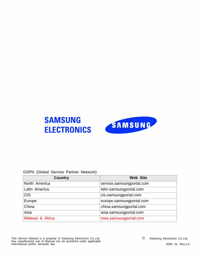
Country Web SiteNorth America service.samsungportal.comLatin America latin.samsungportal.comCIS cis.samsungportal.comEurope europe.samsungportal.comChina china.samsungportal.comAsia asia.samsungportal.comMideast & Africa mea.samsungportal.com
GSPN (Global Service Partner Network)

SAMSUNG Proprietary-Contents may change without notice
1. Safety Precautions
1-1
This Document can not be used without Samsung's authorization
1-1. Repair Precaution
― Repair in Shield Box, during detailed tuning.Take specially care of tuning or test, because the specification of cellular phone is sensitive forsurrounding interference(RF noise).
― Be careful to use a kind of magnetic object or tool, because performance of parts is damaged bythe influence of magnetic force.
― Surely use a standard screwdriver when you disassemble this product, otherwise screw will beworn away.
― Use a thicken twisted wire when you measure level.A thicken twisted wire has low resistance, therefore error of measurement is few.
― Repair after separate Test Pack and Set because for short danger (for example an overcurrentand furious flames of parts etc) when you repair board in condition of connecting Test Pack andtuning on.
― Take specially care of soldering, because Land of PCB is small and weak in heat.
― Surely tune on/off while using AC power plug, because a repair of battery charger is dangerouswhen tuning ON/OFF PBA and Connector after disassembling charger.
― Don't use as you pleases after change other material than replacement registered on SEC System.Otherwise engineer in charge isn't charged with problem that you don't keep this rules.
SAMSUNG Proprietary-Contents may change without notice
Safety Precautions
1-2
This Document can not be used without Samsung's authorization
1-2. ESD(Electrostatically Sensitive Devices) Precaution
Several semiconductor may be damaged easily by static electricity. Such parts are called by ESD(Electrostatically Sensitive Devices), for example IC,BGA chip etc. Read Precaution below.You can prevent from ESD damage by static electricity.
― Remove static electricity remained your body before you touch semiconductor or parts withsemiconductor. There are ways that you touch an earthed place or wear static electricity preventionstring on wrist.
― Use earthed soldering steel when you connect or disconnect ESD.
― Use soldering removing tool to break static electricity. Otherwise ESD will be damaged by staticelectricity.
― Don't unpack until you set up ESD on product. Because most of ESD are packed by box andaluminum plate to have conductive power,they are prevented from static electricity.
― You must maintain electric contact between ESD and place due to be set up until ESD isconnected completely to the proper place or a circuit board.
SAMSUNG Proprietary-Contents may change without notice
2. Specification
This Document can not be used without Samsung's authorization
2-1
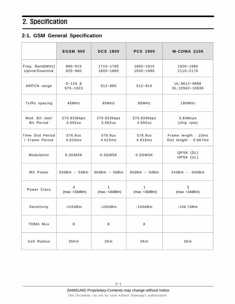
EGSM 900 DCS 1800 PCS 1900 W-CDMA 2100
Freq. Band[MHz]Upl ink/Downl ink
880~915925~960
1710~17851805~1880
1850~19101930~1990
1920~19802110~2170
ARFCN range0~124 &
975~1023512~885 512~810
UL:9612~9888DL:10562~10838
Tx/Rx spacing 45MHz 95MHz 80MHz 190MHz
Mod. Bit rate/Bi t Per iod
270.833kbps3.692us
270.833kbps3.692us
270.833kbps3.692us
3.84Mcps(chip rate)
Time Slot Per iod/ Frame Period
576.9us4.615ms
576.9us4.615ms
576.9us4.615ms
Frame length : 10msSlot length : 0.667ms
Modulat ion 0.3GMSK 0.3GMSK 0.3GMSKQPSK (DL)HPSK (UL)
MS Power 33dBm ~ 5dBm 30dBm ~ 0dBm 30dBm ~ 0dBm 24dBm ~ -50dBm
Power Class4
(max +33dBm)1
(max +30dBm)1
(max +30dBm)3
(max +24dBm)
Sensi t iv i ty -102dBm -100dBm -100dBm -106.7dBm
TDMA Mux 8 8 8
Cel l Radius 35Km 2Km 2Km 2Km
2-1. GSM General Specification
SAMSUNG Proprietary-Contents may change without noticeThis Document can not be used without Samsung's authorization
Specification
2-2
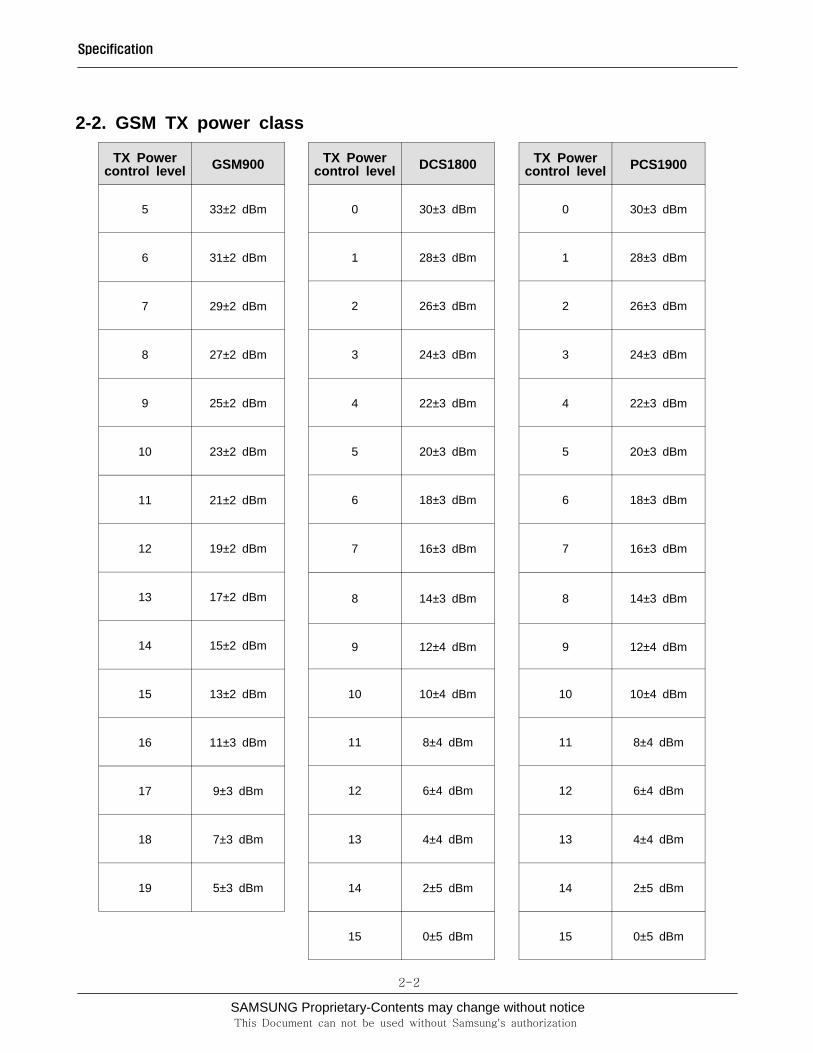
TX Powercontrol level PCS1900
0 30±3 dBm
1 28±3 dBm
2 26±3 dBm
3 24±3 dBm
4 22±3 dBm
5 20±3 dBm
6 18±3 dBm
7 16±3 dBm
8 14±3 dBm
9 12±4 dBm
10 10±4 dBm
11 8±4 dBm
12 6±4 dBm
13 4±4 dBm
14 2±5 dBm
15 0±5 dBm
TX Powercontrol level GSM900
5 33±2 dBm
6 31±2 dBm
7 29±2 dBm
8 27±2 dBm
9 25±2 dBm
10 23±2 dBm
11 21±2 dBm
12 19±2 dBm
13 17±2 dBm
14 15±2 dBm
15 13±2 dBm
16 11±3 dBm
17 9±3 dBm
18 7±3 dBm
19 5±3 dBm
TX Powercontrol level DCS1800
0 30±3 dBm
1 28±3 dBm
2 26±3 dBm
3 24±3 dBm
4 22±3 dBm
5 20±3 dBm
6 18±3 dBm
7 16±3 dBm
8 14±3 dBm
9 12±4 dBm
10 10±4 dBm
11 8±4 dBm
12 6±4 dBm
13 4±4 dBm
14 2±5 dBm
15 0±5 dBm
2-2. GSM TX power class
SAMSUNG Proprietary-Contents may change without notice
3. Product Function
3-1
This Document can not be used without Samsung's authorization
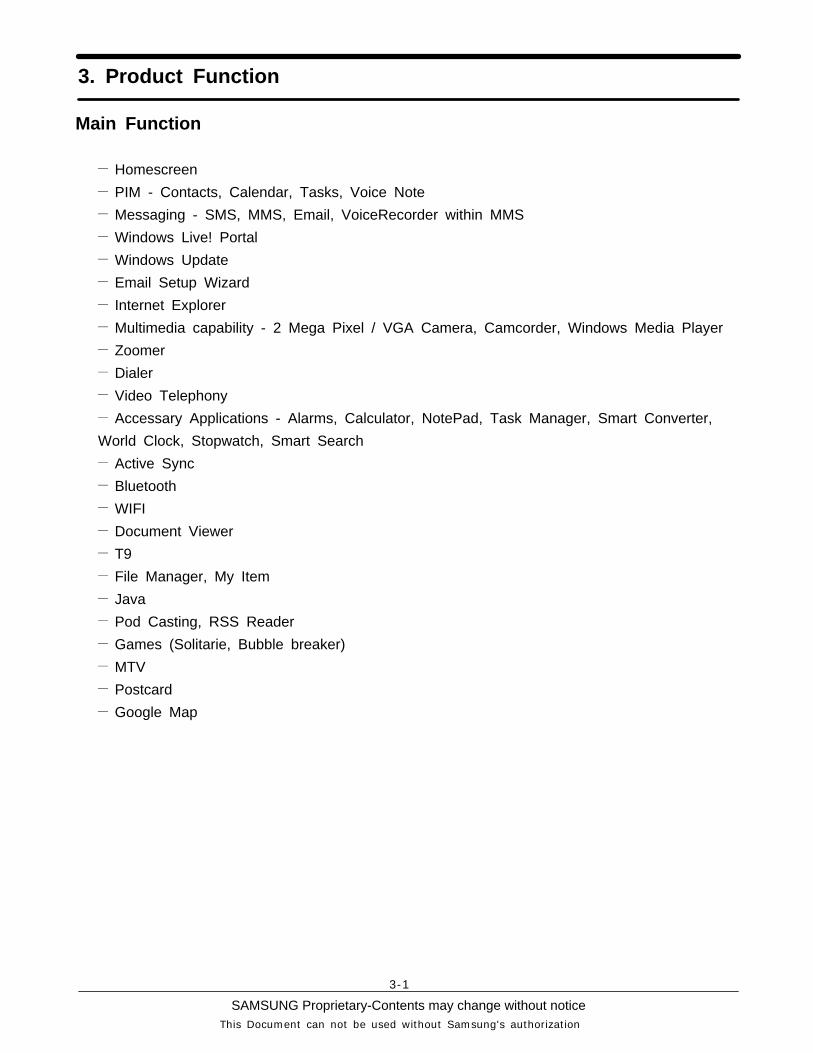
Main Function
― Homescreen― PIM - Contacts, Calendar, Tasks, Voice Note― Messaging - SMS, MMS, Email, VoiceRecorder within MMS― Windows Live! Portal― Windows Update― Email Setup Wizard― Internet Explorer― Multimedia capability - 2 Mega Pixel / VGA Camera, Camcorder, Windows Media Player― Zoomer― Dialer― Video Telephony― Accessary Applications - Alarms, Calculator, NotePad, Task Manager, Smart Converter,World Clock, Stopwatch, Smart Search― Active Sync― Bluetooth― WIFI― Document Viewer― T9― File Manager, My Item― Java― Pod Casting, RSS Reader― Games (Solitarie, Bubble breaker)― MTV― Postcard― Google Map

SAMSUNG Proprietary-Contents may change without notice
Product Function
3-2
This Document can not be used without Samsung's authorization

SAMSUNG Proprietary-Contents may change without notice
4. Array course control
4-1
This Document can not be used without Samsung's authorization
4-1. Software AdjustmentsThere is 2 set to download the binary image into your device.
[First set]
1. JIG BOX (UMTS TEST JIG: GH80-03308A)2. USB Cable : JIG to PC3. Test Cable : JIG to SGH-i780 (GH39-00890A)4. Power Cable : JIG to power supply5. Serial Cable : SGH-i780 to PC6. Power Supply7. RF Cable : SGH-i560 to Agilent 8960 or CMU200 (GH39-00599A)8. Test Cable : JIG to SGH-i780 (GH39-00886A)

SAMSUNG Proprietary-Contents may change without notice
Array course control
4-2
This Document can not be used without Samsung's authorization
[Second set]
1. USB DATA Link Cable : GH39-00922A2. Battery : GH43-02969A
4-2. Software Download
4-2-1. Pre-requisite for Download
• Downloader Program (there are 2 ways to download.)
- [Image version].exe (Single downloader)- SGH_i780V_version.exe (Multi downloader)
• SGH_i780V Mobile Device• USB Driver
- PDA : Samsung MITs USB Sync [Samsung MITs USB Sync.zip]- Phone : Samsung CDMA Modem [Samsung CDMA Modem.zip]
• Driver Installation.- PDA
Make sure that you install drivers.If you installed the latest ActiveSync program, you don’t need to install the pda driver. Pleaseinstall the latest ActiveSync program.
- PhoneWhen you download the phone image, you need the driver of Samsung CDMA Modem.If you want to download the phone image, install the Samsung CDMA Modem driver.After you install the driver of Samsung CDMA Modem, please restart a host computer.
SAMSUNG Proprietary-Contents may change without notice
Array course control
4-3
This Document can not be used without Samsung's authorization
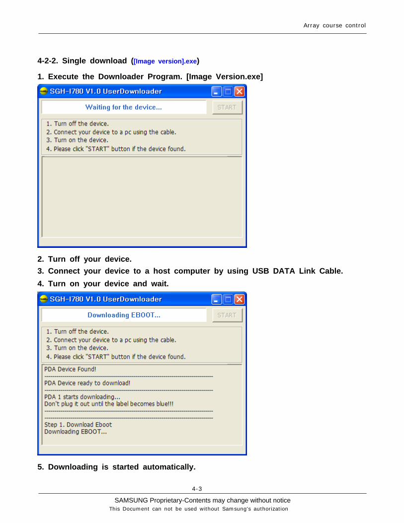
4-2-2. Single download ([Image version].exe)
1. Execute the Downloader Program. [Image Version.exe]
2. Turn off your device.3. Connect your device to a host computer by using USB DATA Link Cable.4. Turn on your device and wait.
5. Downloading is started automatically.

SAMSUNG Proprietary-Contents may change without notice
Array course control
4-4
This Document can not be used without Samsung's authorization
6. When the download is finished, the phone is turned off automatically.
[ Job Done ]
Trouble Shooting 1. “PDA Device not found” message

SAMSUNG Proprietary-Contents may change without notice
Array course control
4-5
This Document can not be used without Samsung's authorization
Make sure that your device is connected a host computer by USB DATA Link cable.
2. “Port Open Failed” message or application hang
After you install “phone USB driver (Samsung CDMA Modem)” at first time, you may see “Portopen failed…” message or application hang while downloading a phone image. If so, terminatethe application and then try the download again.

SAMSUNG Proprietary-Contents may change without notice
Array course control
4-6
This Document can not be used without Samsung's authorization
If USB port is changed, at first time you may see “Port open failed…” message or applicationhang. If so, terminate the application and then try the download again.
If USB cable to the mobile device is not connected tightly, you may see “Port open failed…”message or application hang. If so, terminate the application and then try the download again.
If you always see “port open failed” message or application hang,1. When application is activated, go to the device manager, remove the SAMSUNG CDMA Modem
and SAMSUNG USB Composite Device.2. Rename C:\WINDOWS\system32\drivers\Modem.sys to other name. (ex. Modem-.sys)3. Go to control panel->program add/remove, and then remove Samsung CDMA Modem driver or
Samsung USB driver(MCCI)4. Restart your PC.5. Install attached SAMSUNG CDMA Modem_4.34 6. Try the download again. 3. “Write Failed” message
If battery level is low, use charged battery and try again.

SAMSUNG Proprietary-Contents may change without notice
Array course control
4-7
This Document can not be used without Samsung's authorization
4-2-3. Multi download
1. Device Settings 1. USB 2.0 hub:
Use the D-Link DUB-H7, an authorized Hi-Speed USB 2.0 hub, only. 1) Connect the hub to PC.2) Connect the hub to the adapter.
2. Data Cable: Check the serial number first. The number should start with ‘D.’ 1) Connect the hub to the cable. 2) Connect testing devices to the cable

SAMSUNG Proprietary-Contents may change without notice
Array course control
4-8
This Document can not be used without Samsung's authorization
3. Illustration of MultiDownloader Overall Figure after SettingsConfiguration
2. Prerequisite1. Before beginning the download, make sure all testing devices have the GJ2 or later boot image.Go to the ‘Start à Settings à System à Version’ to check that the version is ‘PDA: i870BVGJ2’ or later. 2. Before beginning the download, confirm that the phone modem of the phone is attached to the
computer USB port of the computer where the OS image will be downloaded. To this end, make sure the phone image has been downloaded only once.(The initial attempt will fail, but this iswill be failed. This is to install the phone modem to the computerUSB port will failof the computer.) Ex) In order to multi-download the OS image for 8 devices, select the phone image only to downloaddownload it to 8 devices. Initially, the download to 8 devices will be failed. However, you will see thatthere are 8 SAMSUNG CDMA modems under "Mthe modem" of in the "Device Manager".(It may take a while to confirm that the modems appear under the "Mmodem"category. If theyappearappeared, they are installed successfully.)
SAMSUNG Proprietary-Contents may change without notice
Array course control
4-9
This Document can not be used without Samsung's authorization
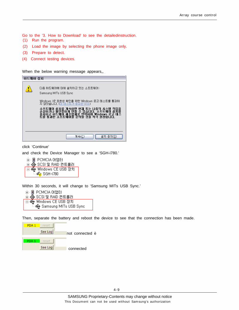
Go to the ‘3. How to Download’ to see the detailedinstruction.(1) Run the program.(2) Load the image by selecting the phone image only.(3) Prepare to detect.(4) Connect testing devices.
When the below warning message appears,,
click ‘Continue’and check the Device Manager to see a ‘SGH-i780.’
Within 30 seconds, it will change to ‘Samsung MITs USB Sync.’
Then, separate the battery and reboot the device to see that the connection has been made.
not connected è
connected

SAMSUNG Proprietary-Contents may change without notice
Array course control
4-10
This Document can not be used without Samsung's authorization
(5) Start downloading(6) Wait until the phone modems appear in the Device Manager.Go to the ‘My Computer à–Properties à–Hardware à– Device Manager à– Modem' to check that theSAMSUNG CDMA Modem appears.
(7) After terminating the program, disconnect the device.(8) Repeat the process from (1)
to confirm that downloading to the phone works appropriately.If several phones do not appear,,repeat the same process until all devices are connected and appear.

SAMSUNG Proprietary-Contents may change without notice
Array course control
4-11
This Document can not be used without Samsung's authorization
3. How to Download1. Disconnecting the ActiveSync
Run the ActiveSync. Then, select the Connection Settings under the ‘File’ tab. Deselect the ‘Allow USB Coneection.’

SAMSUNG Proprietary-Contents may change without notice
Array course control
4-12
This Document can not be used without Samsung's authorization
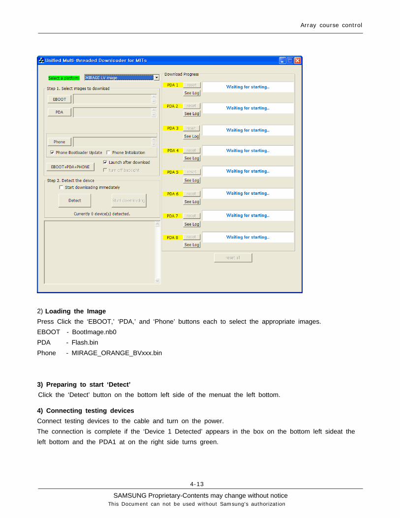
1) Running the programRun the ‘UMDL_i780_v1.0.exe .’
Note, ‘Waiting for starting…’ in the screenshot sounds very odd. I would suggest that the client considerchanging this to ‘Waiting to start…’
Buttons will be activated when the ‘MIRAGE LV Image’ is selected at in the ‘Select a
platform’ menupane.
SAMSUNG Proprietary-Contents may change without notice
Array course control
4-13
This Document can not be used without Samsung's authorization
2) Loading the ImagePress Click the ‘EBOOT,’ ‘PDA,’ and ‘Phone’ buttons each to select the appropriate images.EBOOT - BootImage.nb0PDA - Flash.binPhone - MIRAGE_ORANGE_BVxxx.bin
3) Preparing to start ‘Detect’Click the ‘Detect’ button on the bottom left side of the menuat the left bottom.
4) Connecting testing devicesConnect testing devices to the cable and turn on the power.The connection is complete if the ‘Device 1 Detected’ appears in the box on the bottom left sideat theleft bottom and the PDA1 at on the right side turns green.

SAMSUNG Proprietary-Contents may change without notice
Array course control
4-14
This Document can not be used without Samsung's authorization
Connect all 8 devices as instructedwritten in theabove.NOTE: Connect the devices one by one.Otherwise, an error may occur in the computer USB port of the computer. When this error occurs, go tothe page 22 to see the reference.
5) Starting the download
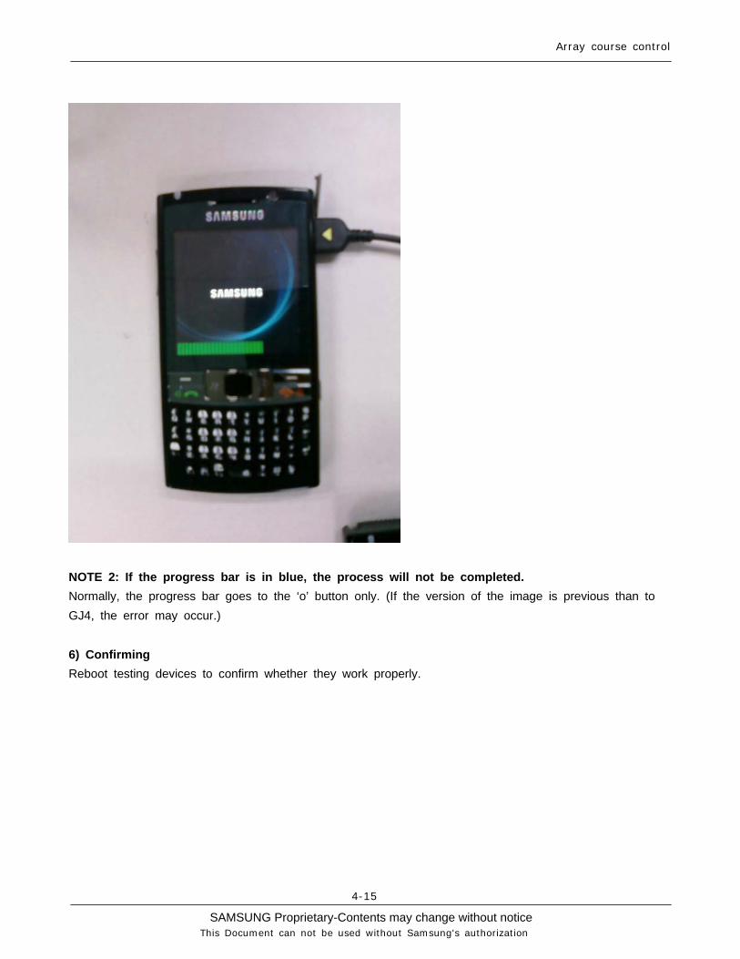
Press Click the ‘Start downloading’ button.
NOTE1: Make sure the progress, shown in by the bar, is completed for eachin a testing device.(The progress of downloading the ‘Flash.bin,’ the PDA image, is shown as the green bar at the bottomof the LCD screen.)
SAMSUNG Proprietary-Contents may change without notice
Array course control
4-15
This Document can not be used without Samsung's authorization
NOTE 2: If the progress bar is in blue, the process will not be completed.Normally, the progress bar goes to the ‘o’ button only. (If the version of the image is previous than toGJ4, the error may occur.)
6) ConfirmingReboot testing devices to confirm whether they work properly.

SAMSUNG Proprietary-Contents may change without notice
Array course control
4-16
This Document can not be used without Samsung's authorization
When the download is complete,,
Click the ‘reset all’ button at on the bottom right sidethe right bottomto reset the downloader.
NOTE: If the download failsis failed,,try once again to downloadsucceed.
SAMSUNG Proprietary-Contents may change without notice
Array course control
4-17
This Document can not be used without Samsung's authorization
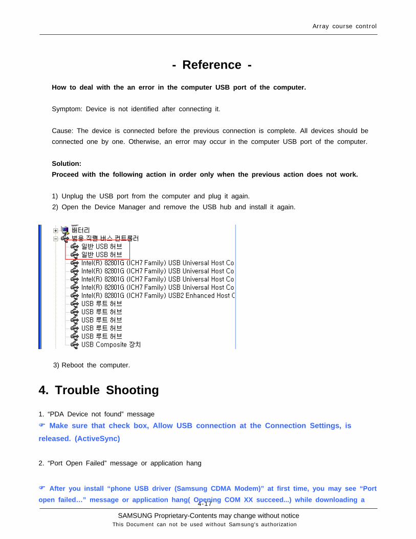
- Reference - How to deal with the an error in the computer USB port of the computer. Symptom: Device is not identified after connecting it. Cause: The device is connected before the previous connection is complete. All devices should beconnected one by one. Otherwise, an error may occur in the computer USB port of the computer. Solution:Proceed with the following action in order only when the previous action does not work. 1) Unplug the USB port from the computer and plug it again.2) Open the Device Manager and remove the USB hub and install it again.
3) Reboot the computer.
4. Trouble Shooting 1. “PDA Device not found” message
Make sure that check box, Allow USB connection at the Connection Settings, isreleased. (ActiveSync)
2. “Port Open Failed” message or application hang
After you install “phone USB driver (Samsung CDMA Modem)” at first time, you may see “Portopen failed…” message or application hang( Opening COM XX succeed...) while downloading a

SAMSUNG Proprietary-Contents may change without notice
Array course control
4-18
This Document can not be used without Samsung's authorization
phone image. If so, terminate the application and then try the download again.
If USB port is changed, at first time you may see “Port open failed…” message or applicationhang( Opening COM XX succeed...). If so, terminate the application and then try the downloadagain.
If USB cable to the mobile device is not connected tightly, you may see “Port open failed…”message or application hang( Opening COM XX succeed...). If so, terminate the application andthen try the download again. 3. “Write Failed” message
If battery level is low, use charged battery and try again.

SAMSUNG Proprietary-Contents may change without notice
5. Exploded View and Parts List
5-3
This Document can not be used without Samsung's authorization
5-1. Cellular phone Exploded View
QME03
QKP01
QFR01
QLC01
QAR01QMP01
QCA02
QVK01
QSH01
QSP01
QMO01
QST01
QCR06QCR08QSC01
QRF01
QBR04
QJK01
QME01
QRE01
QCR08
QBA01
QBA00
QAN02
QSH02QCA01
QCR06
QCB01
QLB01
QVO01
QCK02 QIF01
QCK01QSD01
QMI01

SAMSUNG Proprietary-Contents may change without notice
Exploded View and Parts List
5-2
This Document can not be used without Samsung's authorization
Design LOC Description SEC CODEQAN02 INTENNA-SGHI780 GH42-01329AQAR01 AUDIO-RECEIVER 3009-001308QBA00 ASSY COVER-BATT GH98-07577AQBA01 INNER BATTERY PACK-1480MAH,BLK GH43-02969AQBR04 ASSY BRACKET-SPEAKER GH98-06544AQCA01 CAMERA MODULE GH59-04823AQCA02 CAMERA MODULE GH59-04824AQCB01 CBF COAXIAL CABLE-SGHI780 GH39-00984AQCK01 ASSY KEY-CAMERA GH98-06543AQCK02 PMO KEY-PWR GH72-43404AQCR06 SCREW-MACHINE 6001-001155QCR06 SCREW-MACHINE 6001-001155QCR08 SCREW-MACHINE 6001-001611QCR08 SCREW-MACHINE 6001-001611QFR01 ASSY CASE-FRONT GH98-05794AQIF01 PMO COVER-IF GH72-43402AQJK01 UNIT-OPTICAL JOYSTICK GH59-04912AQKP01 ASSY KEYPAD-(FTM/BLK) GH98-07281AQLB01 ASSY BRACKET-LCD GH98-06545AQLC01 LCD-MODULE SGHI780 GH07-01158AQME01 KEY FPCB-KEY FPCB ASSY GH59-04910AQME03 UNIT-TOUCH PANEL(ORA) GH59-04930AQMI01 AS-SGHI607 MIC GH81-06077AQMO01 MOTOR DC-SGHI780 GH31-00390AQMP01 PBA MAIN-SGHI780 GH92-04221AQRE01 ASSY CASE-REAR GH98-05795AQRF01 TAPE-RF SHEET GH74-35960AQSC01 PMO COVER-SCREW GH72-45115AQSD01 PMO COVER-SD GH72-43401AQSH01 ICT SHIELD-COVER A GH70-02883AQSH02 ICT SHIELD-COVER B GH70-02884AQSP01 MICRO SPEAKER 3001-002311QST01 ASSY ACCE-STYLUS PEN(BLK) GH98-07299AQVK01 KEY FPCB-F.P.C(V/K)ASSY GH59-04905AQVO01 PMO KEY-VOL GH72-43403A
5-2. Cellular phone Parts List
SAMSUNG Proprietary-Contents may change without notice
Exploded View and Parts List
5-3
This Document can not be used without Samsung's authorization
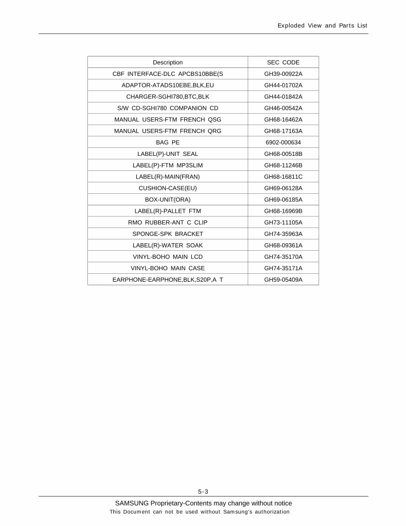
Description SEC CODE
CBF INTERFACE-DLC APCBS10BBE(S GH39-00922A
ADAPTOR-ATADS10EBE,BLK,EU GH44-01702A
CHARGER-SGHI780,BTC,BLK GH44-01842A
S/W CD-SGHI780 COMPANION CD GH46-00542A
MANUAL USERS-FTM FRENCH QSG GH68-16462A
MANUAL USERS-FTM FRENCH QRG GH68-17163A
BAG PE 6902-000634
LABEL(P)-UNIT SEAL GH68-00518B
LABEL(P)-FTM MP3SLIM GH68-11246B
LABEL(R)-MAIN(FRAN) GH68-16811C
CUSHION-CASE(EU) GH69-06128A
BOX-UNIT(ORA) GH69-06185A
LABEL(R)-PALLET FTM GH68-16969B
RMO RUBBER-ANT C CLIP GH73-11105A
SPONGE-SPK BRACKET GH74-35963A
LABEL(R)-WATER SOAK GH68-09361A
VINYL-BOHO MAIN LCD GH74-35170A
VINYL-BOHO MAIN CASE GH74-35171A
EARPHONE-EARPHONE,BLK,S20P,A T GH59-05409A

SAMSUNG Proprietary-Contents may change without notice
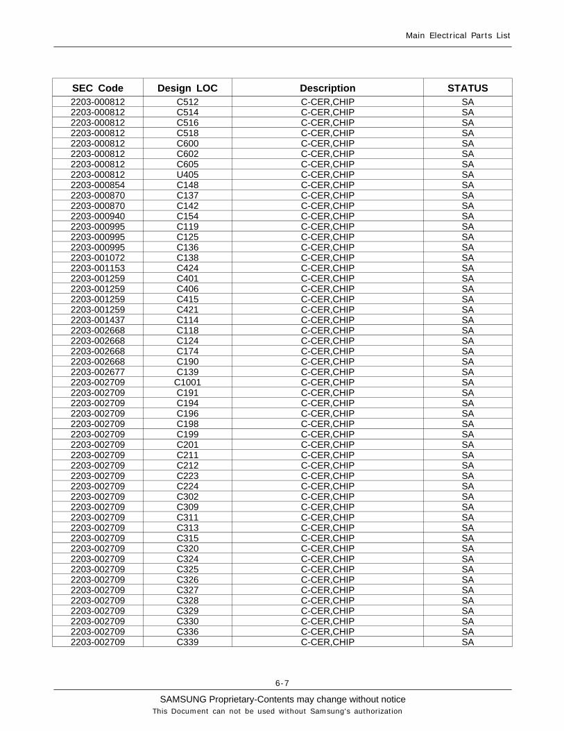
6. Main Electrical Parts List
6-1
This Document can not be used without Samsung's authorization
SEC Code Design LOC Description STATUS0401-001110 D500 DIODE-SWITCHING SA0403-001547 D301 DIODE-ZENER SA0406-001167 ZD600 DIODE-TVS SA0406-001167 ZD601 DIODE-TVS SA0406-001167 ZD602 DIODE-TVS SA0406-001167 ZD603 DIODE-TVS SA0406-001190 ZD506 DIODE-TVS SA0406-001210 ZD403 DIODE-TVS SA0406-001210 ZD404 DIODE-TVS SA0406-001210 ZD405 DIODE-TVS SA0406-001210 ZD406 DIODE-TVS SA0406-001210 ZD408 DIODE-TVS SA0406-001210 ZD605 DIODE-TVS SA0406-001215 ZD300 DIODE-TVS SA0406-001215 ZD301 DIODE-TVS SA0406-001215 ZD407 DIODE-TVS SA0406-001231 D401 DIODE-TVS SA0406-001231 D402 DIODE-TVS SA0406-001231 D600 DIODE-TVS SA0406-001231 D601 DIODE-TVS SA0406-001231 D604 DIODE-TVS SA0406-001231 D605 DIODE-TVS SA0406-001231 D606 DIODE-TVS SA0406-001231 ZD400 DIODE-TVS SA0406-001231 ZD401 DIODE-TVS SA0406-001231 ZD501 DIODE-TVS SA0406-001231 ZD502 DIODE-TVS SA0406-001231 ZD503 DIODE-TVS SA0406-001231 ZD504 DIODE-TVS SA0406-001231 ZD505 DIODE-TVS SA0407-000115 D400 DIODE-ARRAY SA0407-001002 D300 DIODE-ARRAY SA0407-001007 D302 DIODE-ARRAY SA0501-000225 TR600 TR-SMALL SIGNAL SA0501-000225 TR601 TR-SMALL SIGNAL SA0501-000225 TR602 TR-SMALL SIGNAL SA0504-000168 Q300 TR-DIGITAL SA0504-000168 Q301 TR-DIGITAL SA0504-000168 Q303 TR-DIGITAL SA0505-001165 Q302 FET-SILICON SA0601-001905 LED600 LED SA0801-002237 U202 IC-CMOS LOGIC SA0801-002529 U203 IC-CMOS LOGIC SA0801-002800 U205 IC-CMOS LOGIC SA0801-002800 U303 IC-CMOS LOGIC SA0801-002800 U307 IC-CMOS LOGIC SA0801-002800 U500 IC-CMOS LOGIC SA0801-002800 U518 IC-CMOS LOGIC SA0801-002882 U305 IC-CMOS LOGIC SA0801-003013 U200 IC-CMOS LOGIC SA0801-003013 U601 IC-CMOS LOGIC SA0801-003013 U602 IC-CMOS LOGIC SA0801-003052 U204 IC-CMOS LOGIC SA

SAMSUNG Proprietary-Contents may change without notice
Main Electrical Parts List
6-2
This Document can not be used without Samsung's authorization
SEC Code Design LOC Description STATUS0801-003052 U508 IC-CMOS LOGIC SA0801-003076 U201 IC-CMOS LOGIC SA0902-002235 UCP700 IC-MICROPROCESSOR SA0909-001056 U503 IC-REAL TIME CLOCK SA1001-001336 U502 IC-ANALOG SWITCH SA1001-001362 U402 IC-ANALOG SWITCH SA1001-001362 U403 IC-ANALOG SWITCH SA1001-001401 U501 IC-ANALOG SWITCH SA1002-001410 U406 IC-D/A CONVERTER SA1006-001322 U600 IC-LINE TRANSCEIVER SA1106-001564 UME201 IC-SRAM SA1108-000127 UME200 IC-MCP SA1201-002446 PAM100 IC-POWER AMP SA1201-002531 PAM101 IC-POWER AMP SA1201-002587 U400 IC-AUDIO AMP SA1203-002785 U507 IC-VOL. DETECTOR SA1203-002832 U308 IC-VOL. DETECTOR SA1203-003328 U514 IC-DC/DC CONVERTER SA1203-003531 U506 IC-POSI.FIXED REG. SA1203-003643 U511 IC-MULTI REG. SA1203-003664 U512 IC-MULTI REG. SA1203-003664 U515 IC-MULTI REG. SA1203-003664 U516 IC-MULTI REG. SA1203-003748 U510 IC-MULTI REG. SA1203-003926 U306 IC-VOL. DETECTOR SA1203-004395 U517 IC-POSI.FIXED REG. SA1203-004435 U509 IC-MULTI REG. SA1203-004435 U513 IC-MULTI REG. SA1203-004606 U505 IC-MULTI REG. SA1203-004763 U519 IC-VOL. DETECTOR SA1203-004838 U301 IC-BATTERY SA1203-004841 U309 IC-POWER SUPERVISOR SA1203-004926 U302 IC-POWER SUPERVISOR SA1205-002720 UCD400 IC-CODEC SA1205-002767 U300 IC-SWITCH SA1205-003215 UCP200 IC-MODEM SA1205-003285 U100 IC-TRANSCEIVER SA1205-003286 U101 IC-RECEIVER SA1205-003316 U504 IC-INTERFACE SA1404-001221 VR400 THERMISTOR-NTC SA2007-000070 R300 R-CHIP SA2007-000138 R115 R-CHIP SA2007-000138 R132 R-CHIP SA2007-000138 R136 R-CHIP SA2007-000138 R141 R-CHIP SA2007-000140 R520 R-CHIP SA2007-000141 R113 R-CHIP SA2007-000141 R206 R-CHIP SA2007-000148 R703 R-CHIP SA2007-000148 R706 R-CHIP SA2007-000148 R712 R-CHIP SA2007-000157 R302 R-CHIP SA2007-000162 R139 R-CHIP SA

SAMSUNG Proprietary-Contents may change without notice
Main Electrical Parts List
6-3
This Document can not be used without Samsung's authorization
SEC Code Design LOC Description STATUS2007-000162 R140 R-CHIP SA2007-000162 R142 R-CHIP SA2007-000162 R146 R-CHIP SA2007-000162 R149 R-CHIP SA2007-000162 R303 R-CHIP SA2007-000162 R304 R-CHIP SA2007-000162 R320 R-CHIP SA2007-000162 R328 R-CHIP SA2007-000162 R512 R-CHIP SA2007-000162 R704 R-CHIP SA2007-000165 R312 R-CHIP SA2007-000168 R212 R-CHIP SA2007-000170 R329 R-CHIP SA2007-000170 R501 R-CHIP SA2007-000170 R607 R-CHIP SA2007-000171 R103 R-CHIP SA2007-000171 R105 R-CHIP SA2007-000171 R109 R-CHIP SA2007-000171 R121 R-CHIP SA2007-000171 R125 R-CHIP SA2007-000171 R127 R-CHIP SA2007-000171 R131 R-CHIP SA2007-000171 R135 R-CHIP SA2007-000171 R150 R-CHIP SA2007-000171 R151 R-CHIP SA2007-000171 R330 R-CHIP SA2007-000171 R403 R-CHIP SA2007-000171 R404 R-CHIP SA2007-000171 R410 R-CHIP SA2007-000171 R513 R-CHIP SA2007-000171 R702 R-CHIP SA2007-000171 R705 R-CHIP SA2007-000171 R707 R-CHIP SA2007-000172 R100 R-CHIP SA2007-000172 R122 R-CHIP SA2007-000174 R106 R-CHIP SA2007-001284 R123 R-CHIP SA2007-001290 R208 R-CHIP SA2007-001298 R116 R-CHIP SA2007-001298 R130 R-CHIP SA2007-001298 R305 R-CHIP SA2007-001298 R306 R-CHIP SA2007-001305 R107 R-CHIP SA2007-001305 R108 R-CHIP SA2007-001305 R117 R-CHIP SA2007-001305 R118 R-CHIP SA2007-001308 R124 R-CHIP SA2007-001319 R709 R-CHIP SA2007-001319 R710 R-CHIP SA2007-003010 R506 R-CHIP SA2007-003010 R510 R-CHIP SA2007-003010 R511 R-CHIP SA2007-003015 R102 R-CHIP SA

SAMSUNG Proprietary-Contents may change without notice
Main Electrical Parts List
6-4
This Document can not be used without Samsung's authorization
SEC Code Design LOC Description STATUS2007-003015 R110 R-CHIP SA2007-007009 R133 R-CHIP SA2007-007014 R313 R-CHIP SA2007-007014 R314 R-CHIP SA2007-007107 R210 R-CHIP SA2007-007107 R211 R-CHIP SA2007-007107 R401 R-CHIP SA2007-007107 R402 R-CHIP SA2007-007107 R412 R-CHIP SA2007-007107 R516 R-CHIP SA2007-007107 R517 R-CHIP SA2007-007107 R518 R-CHIP SA2007-007132 R319 R-CHIP SA2007-007132 R503 R-CHIP SA2007-007137 R317 R-CHIP SA2007-007137 R318 R-CHIP SA2007-007142 R143 R-CHIP SA2007-007142 R144 R-CHIP SA2007-007142 R200 R-CHIP SA2007-007142 R203 R-CHIP SA2007-007142 R204 R-CHIP SA2007-007142 R205 R-CHIP SA2007-007142 R301 R-CHIP SA2007-007142 R323 R-CHIP SA2007-007142 R500 R-CHIP SA2007-007142 R519 R-CHIP SA2007-007142 R602 R-CHIP SA2007-007142 R603 R-CHIP SA2007-007148 R332 R-CHIP SA2007-007155 R413 R-CHIP SNA2007-007155 R420 R-CHIP SNA2007-007193 R101 R-CHIP SA2007-007193 R111 R-CHIP SA2007-007306 R213 R-CHIP SA2007-007309 R104 R-CHIP SA2007-007314 R126 R-CHIP SA2007-007316 R207 R-CHIP SA2007-007316 R307 R-CHIP SA2007-007316 R309 R-CHIP SA2007-007317 R507 R-CHIP SA2007-007317 R509 R-CHIP SA2007-007318 R315 R-CHIP SA2007-007318 R515 R-CHIP SA2007-007318 R600 R-CHIP SA2007-007318 R605 R-CHIP SA2007-007318 R608 R-CHIP SA2007-007405 R308 R-CHIP SA2007-007468 R310 R-CHIP SA2007-007468 R409 R-CHIP SA2007-007491 R120 R-CHIP SA2007-007528 R414 R-CHIP SA2007-007528 R419 R-CHIP SA2007-007589 R326 R-CHIP SA

SAMSUNG Proprietary-Contents may change without notice
Main Electrical Parts List
6-5
This Document can not be used without Samsung's authorization
SEC Code Design LOC Description STATUS2007-007698 R502 R-CHIP SA2007-007766 R119 R-CHIP SA2007-007798 R514 R-CHIP SA2007-007798 R604 R-CHIP SA2007-007798 R606 R-CHIP SA2007-007942 R209 R-CHIP SA2007-007942 R327 R-CHIP SA2007-007981 R708 R-CHIP SA2007-007981 R711 R-CHIP SA2007-008015 R601 R-CHIP SA2007-008456 R508 R-CHIP SA2007-008531 R114 R-CHIP SA2007-008544 R112 R-CHIP SA2007-008672 R411 R-CHIP SA2007-008708 R701 R-CHIP SA2007-008739 R321 R-CHIP SA2007-008739 R322 R-CHIP SA2007-008739 R324 R-CHIP SA2007-008739 R325 R-CHIP SA2007-008806 R134 R-CHIP SA2203-000233 C110 C-CER,CHIP SA2203-000233 C157 C-CER,CHIP SA2203-000233 C158 C-CER,CHIP SA2203-000233 C164 C-CER,CHIP SA2203-000233 C166 C-CER,CHIP SA2203-000233 C167 C-CER,CHIP SA2203-000233 C169 C-CER,CHIP SA2203-000233 C170 C-CER,CHIP SA2203-000233 C178 C-CER,CHIP SA2203-000233 C181 C-CER,CHIP SA2203-000233 C182 C-CER,CHIP SA2203-000233 C503 C-CER,CHIP SA2203-000254 C1004 C-CER,CHIP SA2203-000254 C149 C-CER,CHIP SA2203-000254 C156 C-CER,CHIP SA2203-000254 C193 C-CER,CHIP SA2203-000254 C204 C-CER,CHIP SA2203-000254 C207 C-CER,CHIP SA2203-000254 C214 C-CER,CHIP SA2203-000254 C215 C-CER,CHIP SA2203-000254 C225 C-CER,CHIP SA2203-000254 C229 C-CER,CHIP SA2203-000254 C232 C-CER,CHIP SA2203-000254 C238 C-CER,CHIP SA2203-000254 C242 C-CER,CHIP SA2203-000254 C704 C-CER,CHIP SA2203-000254 C710 C-CER,CHIP SA2203-000254 C714 C-CER,CHIP SA2203-000254 C719 C-CER,CHIP SA2203-000254 C736 C-CER,CHIP SA2203-000311 C611 C-CER,CHIP SA2203-000311 C612 C-CER,CHIP SA2203-000311 C614 C-CER,CHIP SA
SAMSUNG Proprietary-Contents may change without notice
Main Electrical Parts List
6-6
This Document can not be used without Samsung's authorization
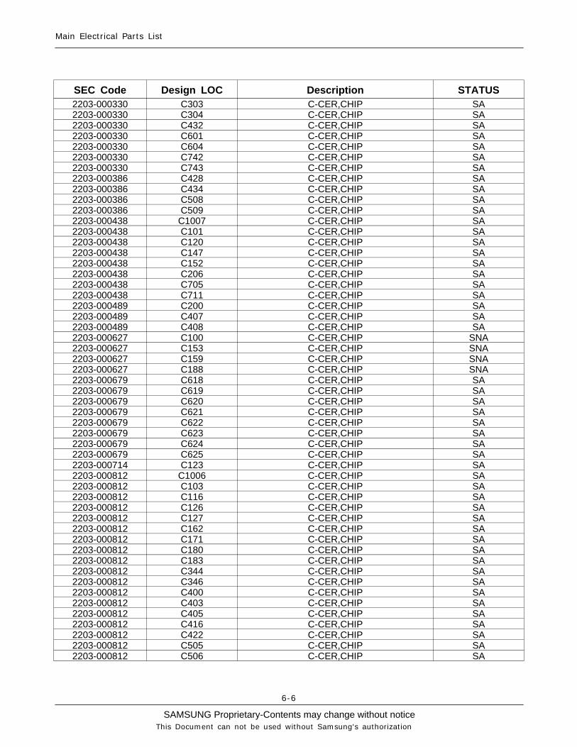
SEC Code Design LOC Description STATUS2203-000330 C303 C-CER,CHIP SA2203-000330 C304 C-CER,CHIP SA2203-000330 C432 C-CER,CHIP SA2203-000330 C601 C-CER,CHIP SA2203-000330 C604 C-CER,CHIP SA2203-000330 C742 C-CER,CHIP SA2203-000330 C743 C-CER,CHIP SA2203-000386 C428 C-CER,CHIP SA2203-000386 C434 C-CER,CHIP SA2203-000386 C508 C-CER,CHIP SA2203-000386 C509 C-CER,CHIP SA2203-000438 C1007 C-CER,CHIP SA2203-000438 C101 C-CER,CHIP SA2203-000438 C120 C-CER,CHIP SA2203-000438 C147 C-CER,CHIP SA2203-000438 C152 C-CER,CHIP SA2203-000438 C206 C-CER,CHIP SA2203-000438 C705 C-CER,CHIP SA2203-000438 C711 C-CER,CHIP SA2203-000489 C200 C-CER,CHIP SA2203-000489 C407 C-CER,CHIP SA2203-000489 C408 C-CER,CHIP SA2203-000627 C100 C-CER,CHIP SNA2203-000627 C153 C-CER,CHIP SNA2203-000627 C159 C-CER,CHIP SNA2203-000627 C188 C-CER,CHIP SNA2203-000679 C618 C-CER,CHIP SA2203-000679 C619 C-CER,CHIP SA2203-000679 C620 C-CER,CHIP SA2203-000679 C621 C-CER,CHIP SA2203-000679 C622 C-CER,CHIP SA2203-000679 C623 C-CER,CHIP SA2203-000679 C624 C-CER,CHIP SA2203-000679 C625 C-CER,CHIP SA2203-000714 C123 C-CER,CHIP SA2203-000812 C1006 C-CER,CHIP SA2203-000812 C103 C-CER,CHIP SA2203-000812 C116 C-CER,CHIP SA2203-000812 C126 C-CER,CHIP SA2203-000812 C127 C-CER,CHIP SA2203-000812 C162 C-CER,CHIP SA2203-000812 C171 C-CER,CHIP SA2203-000812 C180 C-CER,CHIP SA2203-000812 C183 C-CER,CHIP SA2203-000812 C344 C-CER,CHIP SA2203-000812 C346 C-CER,CHIP SA2203-000812 C400 C-CER,CHIP SA2203-000812 C403 C-CER,CHIP SA2203-000812 C405 C-CER,CHIP SA2203-000812 C416 C-CER,CHIP SA2203-000812 C422 C-CER,CHIP SA2203-000812 C505 C-CER,CHIP SA2203-000812 C506 C-CER,CHIP SA
SAMSUNG Proprietary-Contents may change without notice
Main Electrical Parts List
6-7
This Document can not be used without Samsung's authorization
SEC Code Design LOC Description STATUS2203-000812 C512 C-CER,CHIP SA2203-000812 C514 C-CER,CHIP SA2203-000812 C516 C-CER,CHIP SA2203-000812 C518 C-CER,CHIP SA2203-000812 C600 C-CER,CHIP SA2203-000812 C602 C-CER,CHIP SA2203-000812 C605 C-CER,CHIP SA2203-000812 U405 C-CER,CHIP SA2203-000854 C148 C-CER,CHIP SA2203-000870 C137 C-CER,CHIP SA2203-000870 C142 C-CER,CHIP SA2203-000940 C154 C-CER,CHIP SA2203-000995 C119 C-CER,CHIP SA2203-000995 C125 C-CER,CHIP SA2203-000995 C136 C-CER,CHIP SA2203-001072 C138 C-CER,CHIP SA2203-001153 C424 C-CER,CHIP SA2203-001259 C401 C-CER,CHIP SA2203-001259 C406 C-CER,CHIP SA2203-001259 C415 C-CER,CHIP SA2203-001259 C421 C-CER,CHIP SA2203-001437 C114 C-CER,CHIP SA2203-002668 C118 C-CER,CHIP SA2203-002668 C124 C-CER,CHIP SA2203-002668 C174 C-CER,CHIP SA2203-002668 C190 C-CER,CHIP SA2203-002677 C139 C-CER,CHIP SA2203-002709 C1001 C-CER,CHIP SA2203-002709 C191 C-CER,CHIP SA2203-002709 C194 C-CER,CHIP SA2203-002709 C196 C-CER,CHIP SA2203-002709 C198 C-CER,CHIP SA2203-002709 C199 C-CER,CHIP SA2203-002709 C201 C-CER,CHIP SA2203-002709 C211 C-CER,CHIP SA2203-002709 C212 C-CER,CHIP SA2203-002709 C223 C-CER,CHIP SA2203-002709 C224 C-CER,CHIP SA2203-002709 C302 C-CER,CHIP SA2203-002709 C309 C-CER,CHIP SA2203-002709 C311 C-CER,CHIP SA2203-002709 C313 C-CER,CHIP SA2203-002709 C315 C-CER,CHIP SA2203-002709 C320 C-CER,CHIP SA2203-002709 C324 C-CER,CHIP SA2203-002709 C325 C-CER,CHIP SA2203-002709 C326 C-CER,CHIP SA2203-002709 C327 C-CER,CHIP SA2203-002709 C328 C-CER,CHIP SA2203-002709 C329 C-CER,CHIP SA2203-002709 C330 C-CER,CHIP SA2203-002709 C336 C-CER,CHIP SA2203-002709 C339 C-CER,CHIP SA

SAMSUNG Proprietary-Contents may change without notice
Main Electrical Parts List
6-8
This Document can not be used without Samsung's authorization
SEC Code Design LOC Description STATUS2203-002709 C342 C-CER,CHIP SA2203-002709 C343 C-CER,CHIP SA2203-002709 C409 C-CER,CHIP SA2203-002709 C412 C-CER,CHIP SA2203-002709 C435 C-CER,CHIP SA2203-002709 C501 C-CER,CHIP SA2203-002709 C533 C-CER,CHIP SA2203-002709 C561 C-CER,CHIP SA2203-002709 C613 C-CER,CHIP SA2203-002709 C615 C-CER,CHIP SA2203-002709 C616 C-CER,CHIP SA2203-002709 C617 C-CER,CHIP SA2203-002709 C703 C-CER,CHIP SA2203-002709 C708 C-CER,CHIP SA2203-002709 C709 C-CER,CHIP SA2203-002709 C713 C-CER,CHIP SA2203-002709 C718 C-CER,CHIP SA2203-002709 C734 C-CER,CHIP SA2203-002709 C735 C-CER,CHIP SA2203-002709 C737 C-CER,CHIP SA2203-002709 C738 C-CER,CHIP SA2203-002759 C155 C-CER,CHIP SA2203-002968 C173 C-CER,CHIP SA2203-003054 C510 C-CER,CHIP SA2203-003054 C511 C-CER,CHIP SA2203-003054 C513 C-CER,CHIP SA2203-003054 C515 C-CER,CHIP SA2203-003054 C517 C-CER,CHIP SA2203-003054 C520 C-CER,CHIP SA2203-003054 C603 C-CER,CHIP SA2203-005281 C186 C-CER,CHIP SA2203-005288 C109 C-CER,CHIP SA2203-005382 C112 C-CER,CHIP SA2203-005382 C113 C-CER,CHIP SA2203-005393 C184 C-CER,CHIP SA2203-005481 C210 C-CER,CHIP SA2203-005482 C189 C-CER,CHIP SA2203-005482 C197 C-CER,CHIP SA2203-005482 C213 C-CER,CHIP SA2203-005482 C248 C-CER,CHIP SA2203-005482 C426 C-CER,CHIP SA2203-005659 C104 C-CER,CHIP SA2203-005659 C105 C-CER,CHIP SA2203-005659 C106 C-CER,CHIP SA2203-005659 C107 C-CER,CHIP SA2203-005725 C133 C-CER,CHIP SA2203-005725 C135 C-CER,CHIP SA2203-005725 C150 C-CER,CHIP SA2203-005727 C111 C-CER,CHIP SA2203-005736 C134 C-CER,CHIP SA2203-005736 C151 C-CER,CHIP SA2203-005806 C1002 C-CER,CHIP SNA2203-005806 C1005 C-CER,CHIP SNA
SAMSUNG Proprietary-Contents may change without notice
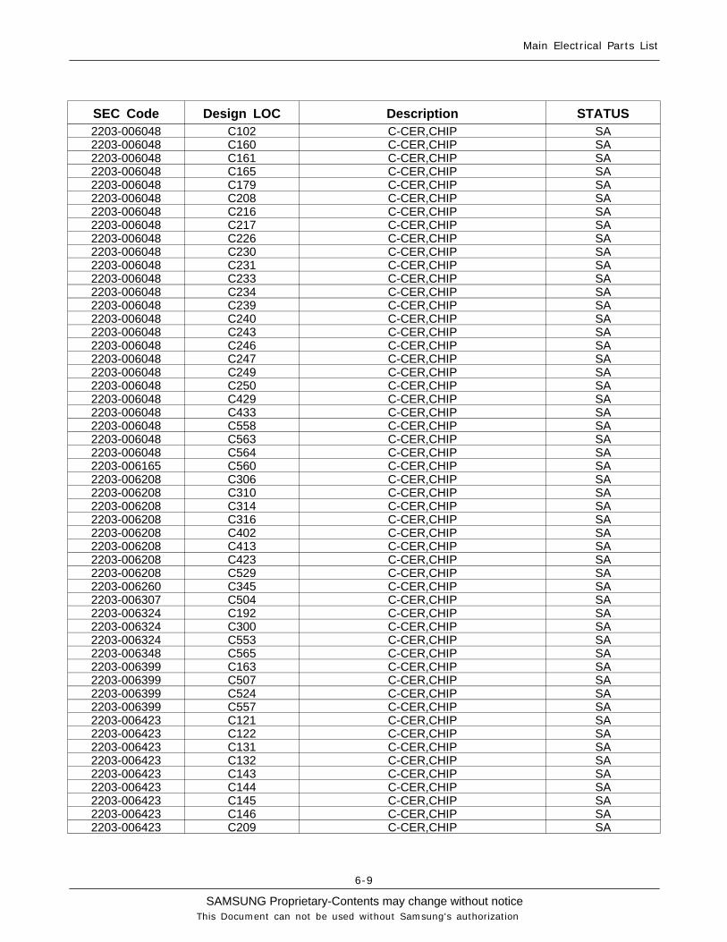
Main Electrical Parts List
6-9
This Document can not be used without Samsung's authorization
SEC Code Design LOC Description STATUS2203-006048 C102 C-CER,CHIP SA2203-006048 C160 C-CER,CHIP SA2203-006048 C161 C-CER,CHIP SA2203-006048 C165 C-CER,CHIP SA2203-006048 C179 C-CER,CHIP SA2203-006048 C208 C-CER,CHIP SA2203-006048 C216 C-CER,CHIP SA2203-006048 C217 C-CER,CHIP SA2203-006048 C226 C-CER,CHIP SA2203-006048 C230 C-CER,CHIP SA2203-006048 C231 C-CER,CHIP SA2203-006048 C233 C-CER,CHIP SA2203-006048 C234 C-CER,CHIP SA2203-006048 C239 C-CER,CHIP SA2203-006048 C240 C-CER,CHIP SA2203-006048 C243 C-CER,CHIP SA2203-006048 C246 C-CER,CHIP SA2203-006048 C247 C-CER,CHIP SA2203-006048 C249 C-CER,CHIP SA2203-006048 C250 C-CER,CHIP SA2203-006048 C429 C-CER,CHIP SA2203-006048 C433 C-CER,CHIP SA2203-006048 C558 C-CER,CHIP SA2203-006048 C563 C-CER,CHIP SA2203-006048 C564 C-CER,CHIP SA2203-006165 C560 C-CER,CHIP SA2203-006208 C306 C-CER,CHIP SA2203-006208 C310 C-CER,CHIP SA2203-006208 C314 C-CER,CHIP SA2203-006208 C316 C-CER,CHIP SA2203-006208 C402 C-CER,CHIP SA2203-006208 C413 C-CER,CHIP SA2203-006208 C423 C-CER,CHIP SA2203-006208 C529 C-CER,CHIP SA2203-006260 C345 C-CER,CHIP SA2203-006307 C504 C-CER,CHIP SA2203-006324 C192 C-CER,CHIP SA2203-006324 C300 C-CER,CHIP SA2203-006324 C553 C-CER,CHIP SA2203-006348 C565 C-CER,CHIP SA2203-006399 C163 C-CER,CHIP SA2203-006399 C507 C-CER,CHIP SA2203-006399 C524 C-CER,CHIP SA2203-006399 C557 C-CER,CHIP SA2203-006423 C121 C-CER,CHIP SA2203-006423 C122 C-CER,CHIP SA2203-006423 C131 C-CER,CHIP SA2203-006423 C132 C-CER,CHIP SA2203-006423 C143 C-CER,CHIP SA2203-006423 C144 C-CER,CHIP SA2203-006423 C145 C-CER,CHIP SA2203-006423 C146 C-CER,CHIP SA2203-006423 C209 C-CER,CHIP SA

SAMSUNG Proprietary-Contents may change without notice
Main Electrical Parts List
6-10
This Document can not be used without Samsung's authorization
SEC Code Design LOC Description STATUS2203-006562 C1000 C-CER,CHIP SA2203-006562 C130 C-CER,CHIP SA2203-006562 C195 C-CER,CHIP SA2203-006562 C202 C-CER,CHIP SA2203-006562 C203 C-CER,CHIP SA2203-006562 C205 C-CER,CHIP SA2203-006562 C218 C-CER,CHIP SA2203-006562 C221 C-CER,CHIP SA2203-006562 C222 C-CER,CHIP SA2203-006562 C227 C-CER,CHIP SA2203-006562 C228 C-CER,CHIP SA2203-006562 C235 C-CER,CHIP SA2203-006562 C236 C-CER,CHIP SA2203-006562 C237 C-CER,CHIP SA2203-006562 C244 C-CER,CHIP SA2203-006562 C245 C-CER,CHIP SA2203-006562 C307 C-CER,CHIP SA2203-006562 C317 C-CER,CHIP SA2203-006562 C318 C-CER,CHIP SA2203-006562 C319 C-CER,CHIP SA2203-006562 C404 C-CER,CHIP SA2203-006562 C419 C-CER,CHIP SA2203-006562 C420 C-CER,CHIP SA2203-006562 C430 C-CER,CHIP SA2203-006562 C431 C-CER,CHIP SA2203-006562 C436 C-CER,CHIP SA2203-006562 C521 C-CER,CHIP SA2203-006562 C527 C-CER,CHIP SA2203-006562 C534 C-CER,CHIP SA2203-006562 C537 C-CER,CHIP SA2203-006562 C540 C-CER,CHIP SA2203-006562 C548 C-CER,CHIP SA2203-006562 C549 C-CER,CHIP SA2203-006562 C550 C-CER,CHIP SA2203-006562 C554 C-CER,CHIP SA2203-006562 C607 C-CER,CHIP SA2203-006562 C609 C-CER,CHIP SA2203-006562 C702 C-CER,CHIP SA2203-006562 C706 C-CER,CHIP SA2203-006562 C707 C-CER,CHIP SA2203-006562 C712 C-CER,CHIP SA2203-006562 C715 C-CER,CHIP SA2203-006562 C717 C-CER,CHIP SA2203-006562 C722 C-CER,CHIP SA2203-006562 C723 C-CER,CHIP SA2203-006562 C724 C-CER,CHIP SA2203-006562 C725 C-CER,CHIP SA2203-006562 C726 C-CER,CHIP SA2203-006562 C727 C-CER,CHIP SA2203-006562 C728 C-CER,CHIP SA2203-006562 C729 C-CER,CHIP SA2203-006562 C730 C-CER,CHIP SA2203-006562 C731 C-CER,CHIP SA

SAMSUNG Proprietary-Contents may change without notice
Main Electrical Parts List
6-11
This Document can not be used without Samsung's authorization
SEC Code Design LOC Description STATUS2203-006562 C732 C-CER,CHIP SA2203-006562 C733 C-CER,CHIP SA2203-006681 C1008 C-CER,CHIP SA2203-006681 C115 C-CER,CHIP SA2203-006681 C176 C-CER,CHIP SA2203-006681 C500 C-CER,CHIP SA2203-006681 C502 C-CER,CHIP SA2203-006681 C519 C-CER,CHIP SA2203-006681 C528 C-CER,CHIP SA2203-006681 C531 C-CER,CHIP SA2203-006681 C716 C-CER,CHIP SA2203-006681 C720 C-CER,CHIP SA2203-006681 C721 C-CER,CHIP SA2203-006824 C117 C-CER,CHIP SA2203-006824 C220 C-CER,CHIP SA2203-006824 C301 C-CER,CHIP SA2203-006824 C321 C-CER,CHIP SA2203-006824 C322 C-CER,CHIP SA2203-006824 C323 C-CER,CHIP SA2203-006824 C331 C-CER,CHIP SA2203-006824 C332 C-CER,CHIP SA2203-006824 C333 C-CER,CHIP SA2203-006824 C337 C-CER,CHIP SA2203-006824 C338 C-CER,CHIP SA2203-006824 C340 C-CER,CHIP SA2203-006824 C347 C-CER,CHIP SA2203-006824 C522 C-CER,CHIP SA2203-006824 C523 C-CER,CHIP SA2203-006824 C525 C-CER,CHIP SA2203-006824 C535 C-CER,CHIP SA2203-006824 C536 C-CER,CHIP SA2203-006824 C538 C-CER,CHIP SA2203-006824 C539 C-CER,CHIP SA2203-006824 C541 C-CER,CHIP SA2203-006824 C542 C-CER,CHIP SA2203-006824 C543 C-CER,CHIP SA2203-006824 C544 C-CER,CHIP SA2203-006824 C545 C-CER,CHIP SA2203-006824 C546 C-CER,CHIP SA2203-006824 C547 C-CER,CHIP SA2203-006824 C551 C-CER,CHIP SA2203-006824 C552 C-CER,CHIP SA2203-006824 C555 C-CER,CHIP SA2203-006824 C556 C-CER,CHIP SA2203-006824 C559 C-CER,CHIP SA2203-006825 C334 C-CER,CHIP SA2203-006825 C335 C-CER,CHIP SA2203-006825 C341 C-CER,CHIP SA2203-006825 C348 C-CER,CHIP SA2203-006837 C172 C-CER,CHIP SA2203-006838 C312 C-CER,CHIP SA2203-006838 C414 C-CER,CHIP SA2203-006838 C425 C-CER,CHIP SA
SAMSUNG Proprietary-Contents may change without notice
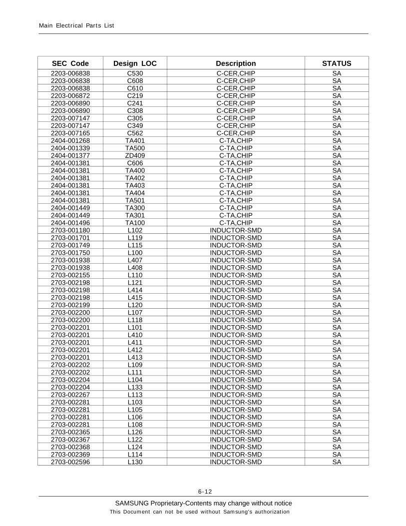
Main Electrical Parts List
6-12
This Document can not be used without Samsung's authorization
SEC Code Design LOC Description STATUS2203-006838 C530 C-CER,CHIP SA2203-006838 C608 C-CER,CHIP SA2203-006838 C610 C-CER,CHIP SA2203-006872 C219 C-CER,CHIP SA2203-006890 C241 C-CER,CHIP SA2203-006890 C308 C-CER,CHIP SA2203-007147 C305 C-CER,CHIP SA2203-007147 C349 C-CER,CHIP SA2203-007165 C562 C-CER,CHIP SA2404-001268 TA401 C-TA,CHIP SA2404-001339 TA500 C-TA,CHIP SA2404-001377 ZD409 C-TA,CHIP SA2404-001381 C606 C-TA,CHIP SA2404-001381 TA400 C-TA,CHIP SA2404-001381 TA402 C-TA,CHIP SA2404-001381 TA403 C-TA,CHIP SA2404-001381 TA404 C-TA,CHIP SA2404-001381 TA501 C-TA,CHIP SA2404-001449 TA300 C-TA,CHIP SA2404-001449 TA301 C-TA,CHIP SA2404-001496 TA100 C-TA,CHIP SA2703-001180 L102 INDUCTOR-SMD SA2703-001701 L119 INDUCTOR-SMD SA2703-001749 L115 INDUCTOR-SMD SA2703-001750 L100 INDUCTOR-SMD SA2703-001938 L407 INDUCTOR-SMD SA2703-001938 L408 INDUCTOR-SMD SA2703-002155 L110 INDUCTOR-SMD SA2703-002198 L121 INDUCTOR-SMD SA2703-002198 L414 INDUCTOR-SMD SA2703-002198 L415 INDUCTOR-SMD SA2703-002199 L120 INDUCTOR-SMD SA2703-002200 L107 INDUCTOR-SMD SA2703-002200 L118 INDUCTOR-SMD SA2703-002201 L101 INDUCTOR-SMD SA2703-002201 L410 INDUCTOR-SMD SA2703-002201 L411 INDUCTOR-SMD SA2703-002201 L412 INDUCTOR-SMD SA2703-002201 L413 INDUCTOR-SMD SA2703-002202 L109 INDUCTOR-SMD SA2703-002202 L111 INDUCTOR-SMD SA2703-002204 L104 INDUCTOR-SMD SA2703-002204 L133 INDUCTOR-SMD SA2703-002267 L113 INDUCTOR-SMD SA2703-002281 L103 INDUCTOR-SMD SA2703-002281 L105 INDUCTOR-SMD SA2703-002281 L106 INDUCTOR-SMD SA2703-002281 L108 INDUCTOR-SMD SA2703-002365 L126 INDUCTOR-SMD SA2703-002367 L122 INDUCTOR-SMD SA2703-002368 L124 INDUCTOR-SMD SA2703-002369 L114 INDUCTOR-SMD SA2703-002596 L130 INDUCTOR-SMD SA

SAMSUNG Proprietary-Contents may change without notice
Main Electrical Parts List
6-13
This Document can not be used without Samsung's authorization
SEC Code Design LOC Description STATUS2703-002798 L112 INDUCTOR-SMD SNA2703-002798 L116 INDUCTOR-SMD SNA2703-002893 L501 INDUCTOR-SMD SA2703-002919 L117 INDUCTOR-SMD SA2703-003182 L304 INDUCTOR-SMD SA2703-003182 L305 INDUCTOR-SMD SA2703-003184 L300 INDUCTOR-SMD SA2703-003184 L301 INDUCTOR-SMD SA2703-003184 L302 INDUCTOR-SMD SA2703-003184 L303 INDUCTOR-SMD SA2703-003240 L306 INDUCTOR-SMD SA2801-004189 OSC700 CRYSTAL-SMD SA2801-004466 OSC300 CRYSTAL-SMD SA2801-004466 OSC500 CRYSTAL-SMD SA2801-004466 OSC701 CRYSTAL-SMD SA2804-001725 OSC400 OSCILLATOR-CLOCK SA2809-001280 TCX100 OSCILLATOR-VCTCXO SA2901-001361 F600 FILTER-EMI/ESD SNA2901-001361 F602 FILTER-EMI/ESD SNA2901-001361 F604 FILTER-EMI/ESD SNA2901-001461 F601 FILTER-EMI/ESD SA2901-001461 F603 FILTER-EMI/ESD SA2904-001629 F105 FILTER-SAW SA2904-001702 F101 FILTER-SAW SA2904-001703 F102 FILTER-SAW SA2904-001738 F103 FILTER-SAW SA2904-001759 F104 FILTER-SAW SA2910-000004 F107 DUPLEXER-FBAR SA2911-000091 F100 DUPLEXER-FEM SA3301-001438 L405 BEAD-SMD SA3301-001438 L406 BEAD-SMD SA3301-001534 L500 BEAD-SMD SA3301-001682 L402 BEAD-SMD SA3301-001682 L403 BEAD-SMD SA3301-001682 L404 BEAD-SMD SA3301-001756 L131 BEAD-SMD SA3301-001789 L400 BEAD-SMD SA3301-001789 L401 BEAD-SMD SA3404-001303 SW600 SWITCH-TACT SA3404-001303 SW601 SWITCH-TACT SA3705-001225 ANT100 CONNECTOR-COAXIAL SA3705-001421 RFS100 CONNECTOR-COAXIAL SA3708-002222 SLC600 CONNECTOR-FPC/FFC/PIC SA3708-002222 SLC601 CONNECTOR-FPC/FFC/PIC SA3708-002283 SLC602 CONNECTOR-FPC/FFC/PIC SA3709-001465 CD300 CONNECTOR-CARD EDGE SA3710-002499 IFC500 SOCKET-INTERFACE SA3711-005296 HDC601 HEADER-BOARD TO BOARD SA3711-005394 HDC600 HEADER-BOARD TO BOARD SA3711-006217 BTC300 HEADER-BATTERY SA3711-006277 HDC602 HEADER-BOARD TO BOARD SA3711-006277 HDC603 HEADER-BOARD TO BOARD SA4202-001356 ANT102 ANTENNA-CHIP SA

SAMSUNG Proprietary-Contents may change without notice
Main Electrical Parts List
6-14
This Document can not be used without Samsung's authorization
SEC Code Design LOC Description STATUS4302-001180 BAT500 BATTERY-LI(2ND) SA4709-001399 F106 COUPLER-DIRECTION SA4709-001527 MOD101 W-LAN MODULE SA4709-001544 MOD100 BLUETOOTH MODULE SAGH71-06620A ANT104 NPR-CONTACT INTENA SAGH71-06620A ANT105 NPR-CONTACT INTENA SAGH71-06620A ANT106 NPR-CONTACT INTENA SAGH71-07813A SC100 NPR SHIELD-FRAME A SAGH71-07814A SC101 NPR SHIELD-FRAME B SA
Please consult the GSPN website (Samsung Portal) for the most recent version of the product'spart list.

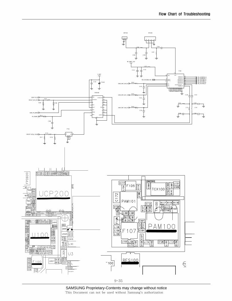
7. Block Diagrams
7-1
7-1. RF Solution Block Diagram
Block Diagrams
7-2
SAMSUNG Proprietary-Contents may change without notice
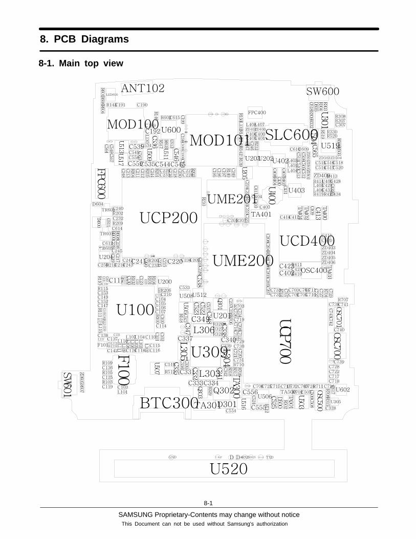
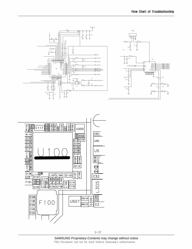
8. PCB Diagrams
8-1
This Document can not be used without Samsung's authorization
8-1. Main top view
SAMSUNG Proprietary-Contents may change without notice
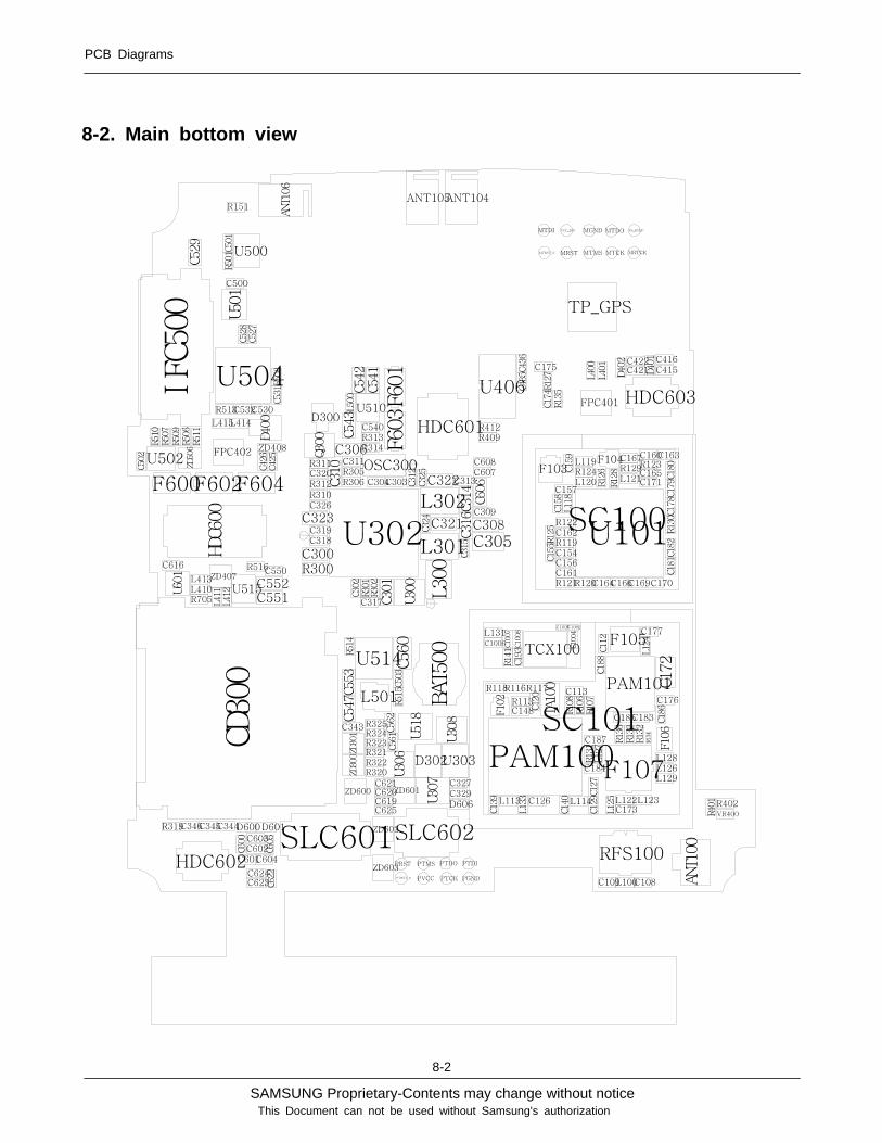
PCB Diagrams
8-2
This Document can not be used without Samsung's authorization
8-2. Main bottom view

SAMSUNG Proprietary-Contents may change without notice
9. Flow Chart of TroubleShooting
9-1
This Document can not be used without Samsung's authorization
9-1. Power OnPDA Part
POWER ON
NG
NO
YES
NO
AT TA301V > 3.32V
Voltage in U309V1 = 2.85~3.3VV2 = 1.8~3.3V
V3 = 1.4VV4 = 1.4VV5 = 1.8V
Battery Change
Check U309 &Neighboring
circuit
Check otherPOWER device

SAMSUNG Proprietary-Contents may change without notice
Flow Chart of Troubleshooting
9-2
This Document can not be used without Samsung's authorization

SAMSUNG Proprietary-Contents may change without notice
Flow Chart of Troubleshooting
9-3
This Document can not be used without Samsung's authorization
PHONE Part
NG
YES
NOYES
NO
YES
NO
YES
1PIN inU301 HIGH?
PHONE ON
OutputPWR
In U302 OK?
1pin inU204 LOW?
6pin inU204 LOW?
Check UME200& Neighboring
Circuit
Check U302 &Neighboring
Circuits
Chcek UCP700& TCX100
Neighboring
Check 6 pinQ302
Check U204

SAMSUNG Proprietary-Contents may change without notice
Flow Chart of Troubleshooting
9-4
This Document can not be used without Samsung's authorization

SAMSUNG Proprietary-Contents may change without notice
Flow Chart of Troubleshooting
9-5
This Document can not be used without Samsung's authorization
SAMSUNG Proprietary-Contents may change without notice
Flow Chart of Troubleshooting
9-6
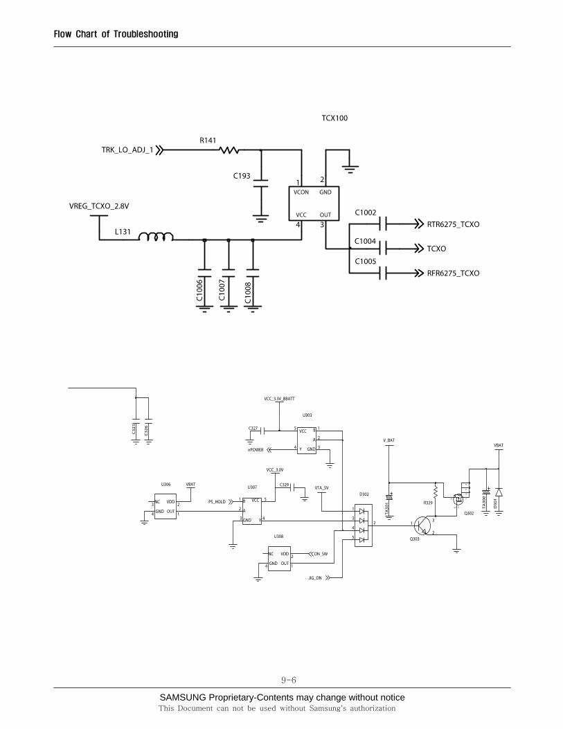
This Document can not be used without Samsung's authorization

SAMSUNG Proprietary-Contents may change without notice
Flow Chart of Troubleshooting
9-7
This Document can not be used without Samsung's authorization

SAMSUNG Proprietary-Contents may change without notice
Flow Chart of Troubleshooting
9-8
This Document can not be used without Samsung's authorization

SAMSUNG Proprietary-Contents may change without notice
Flow Chart of Troubleshooting
9-9
This Document can not be used without Samsung's authorization
9-2. RECEIVER Working
NO
YES
NO
YES
NO
YES YES
NO NO
OPERATEReceiver
RCV-ASSy'Breakdown?
5,6 Pin inU515
Signal On?
35, 36 Pinin UCD400Signal On?
2,4 Pin inU402
Signal On?
Change RCV-Ass'y
CheckUCD400
&Neighboring
Check U402&Neighboring
Circuits
Check U515&
Neighboring
CheckUCP 200

SAMSUNG Proprietary-Contents may change without notice
Flow Chart of Troubleshooting
9-10
This Document can not be used without Samsung's authorization

SAMSUNG Proprietary-Contents may change without notice
Flow Chart of Troubleshooting
9-11
This Document can not be used without Samsung's authorization

SAMSUNG Proprietary-Contents may change without notice
Flow Chart of Troubleshooting
9-12
This Document can not be used without Samsung's authorization

SAMSUNG Proprietary-Contents may change without notice
Flow Chart of Troubleshooting
9-13
This Document can not be used without Samsung's authorization
9-3. SPEAKER Working
NO
YESNO
YES
NO
YES
NO
YES YES
NONO
OPERATESPEAKER
SPK-ASSy' Breakdown?
5, 6 pins inU515
Signal On?
3,4 Pin in U400Signal On?
6, 10 Pin in U402Signal On?
35,36 pins for voice
call &
35, 36, 5 pins for
MP3 in UCD 400
Singal On?
Check UCP 200 forvoice call ,
UCP 700 for Mp3&Neighboring circuits
Change SPK -Ass'y
Check U512 &Neighboring
circuits
Check UCD 400&Neighboring
circuits
Check U402 &Neighboring
circuits
Check U400 &Neighboring
circuits

SAMSUNG Proprietary-Contents may change without notice
Flow Chart of Troubleshooting
9-14
This Document can not be used without Samsung's authorization
SAMSUNG Proprietary-Contents may change without notice
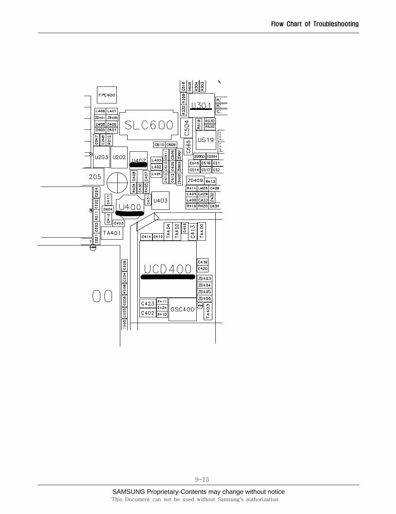
Flow Chart of Troubleshooting
9-15
This Document can not be used without Samsung's authorization
SAMSUNG Proprietary-Contents may change without notice
Flow Chart of Troubleshooting
9-16
This Document can not be used without Samsung's authorization
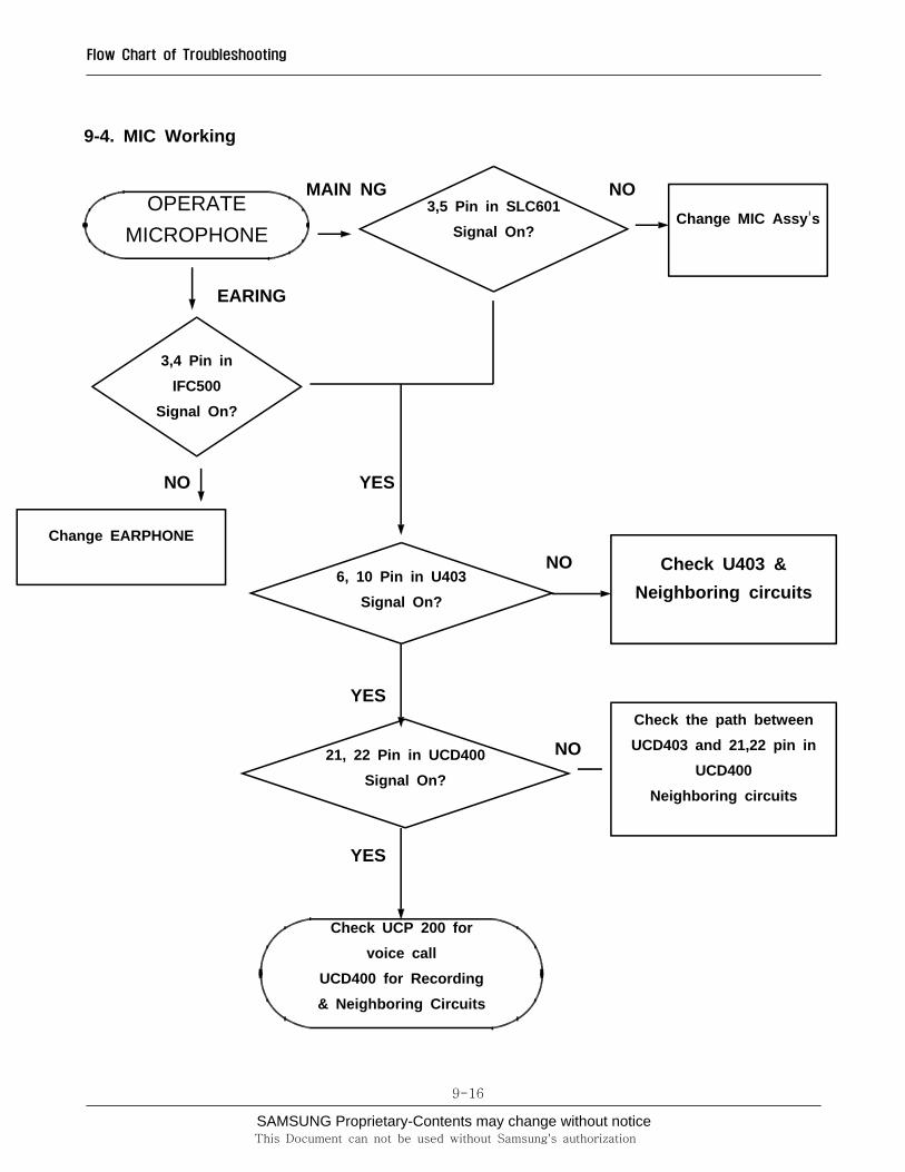
9-4. MIC Working
MAIN NG NO
EARING
NO YES
NO
YES
NO
YES
OPERATEMICROPHONE
3,5 Pin in SLC601Signal On?
Change MIC Assy's
21, 22 Pin in UCD400Signal On?
6, 10 Pin in U403Signal On?
3,4 Pin inIFC500
Signal On?
Check the path betweenUCD403 and 21,22 pin in
UCD400Neighboring circuits
Check U403 &Neighboring circuits
Change EARPHONE
Check UCP 200 forvoice call
UCD400 for Recording& Neighboring Circuits
SAMSUNG Proprietary-Contents may change without notice
Flow Chart of Troubleshooting
9-17
This Document can not be used without Samsung's authorization

SAMSUNG Proprietary-Contents may change without notice
Flow Chart of Troubleshooting
9-18
This Document can not be used without Samsung's authorization

SAMSUNG Proprietary-Contents may change without notice
Flow Chart of Troubleshooting
9-19
This Document can not be used without Samsung's authorization
9-5. KEY Working
YES
NO
YES NO
NOYES
YES
NO NO
YES YES
NO NO
YES YES
NO NO
YES YES
NO
PRESS KEY
POWERKEY NG?
Volumekey NG?
Camerakey NG?
OJ key NG?
QwertyKey NG?
Key FPCBBreakdown?
OJ keyBreakdown?
Key FPCBBreakdown?
Key FPCBBreakdown?
SW600Breakdown?
Check SLC601 &Neighboring Circuit
Change SW600
Check SolderingPAD & Neighboring
Circuit
Change key FPCB
Check SolderingPAD & Neighboring
Circuit
Change key FPCB
Check SLC601 &Neighboring Circuit
Change OJ key
Check SLC602 &Neighboring Circuit
Change key FPCB
SAMSUNG Proprietary-Contents may change without notice
Flow Chart of Troubleshooting
9-20
This Document can not be used without Samsung's authorization

SAMSUNG Proprietary-Contents may change without notice
Flow Chart of Troubleshooting
9-21
This Document can not be used without Samsung's authorization

SAMSUNG Proprietary-Contents may change without notice
Flow Chart of Troubleshooting
9-22
This Document can not be used without Samsung's authorization
9-6. Vibrator Working
OperateVibrator
VibratorBreakdown?
Sodering PADof vibrator any
problem?
pin6 in U512High?
Change Vibrator
Resodering Vibrator
Change U512
Check U512 &Neighboring Circuit
SAMSUNG Proprietary-Contents may change without notice
Flow Chart of Troubleshooting
9-23
This Document can not be used without Samsung's authorization
SAMSUNG Proprietary-Contents may change without notice
Flow Chart of Troubleshooting
9-24
This Document can not be used without Samsung's authorization
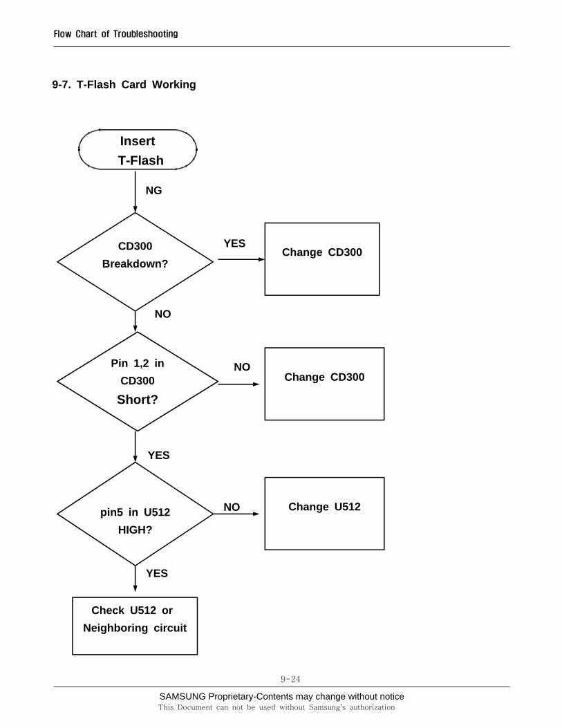
9-7. T-Flash Card Working
NG
YES
NO
NO
YES
NO
YES
InsertT-Flash
CD300Breakdown?
Change CD300
Pin 1,2 inCD300
Short?
pin5 in U512HIGH?
Change U512
Change CD300
Check U512 orNeighboring circuit

SAMSUNG Proprietary-Contents may change without notice
Flow Chart of Troubleshooting
9-25
This Document can not be used without Samsung's authorization
SAMSUNG Proprietary-Contents may change without notice
Flow Chart of Troubleshooting
9-26
This Document can not be used without Samsung's authorization
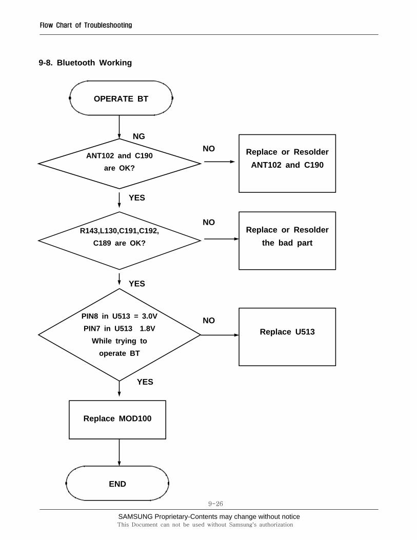
9-8. Bluetooth Working
NGNO
YES
NO
YES
NO
YES
OPERATE BT
R143,L130,C191,C192,C189 are OK?
Replace or ResolderANT102 and C190
ANT102 and C190are OK?
PIN8 in U513 = 3.0VPIN7 in U513 1.8V
While trying tooperate BT
Replace U513
Replace or Resolderthe bad part
Replace MOD100
END

SAMSUNG Proprietary-Contents may change without notice
Flow Chart of Troubleshooting
9-27
This Document can not be used without Samsung's authorization

SAMSUNG Proprietary-Contents may change without notice
Flow Chart of Troubleshooting
9-28
This Document can not be used without Samsung's authorization

SAMSUNG Proprietary-Contents may change without notice
Flow Chart of Troubleshooting
9-29
This Document can not be used without Samsung's authorization
9-9. WLAN Working
NG
NO
YES
NO
YES
NO
YES
YES
OPERATE WLAN
ANT106, R150, R151are OK?
R140,R142 are OK?
PIN4 in U517=3.3VPIN8 in U509=3.0VPIN7 in U509=1.8V
While operating WLAN
WLAN Intenna on RearCase is OK?
Replace or Resolder theANT106, R150, R151
Replace the WLANintenna
Check neighboring circuitand Replace U517,U509
or neighboring parts
Replace or Resolder R140,R142
Replace MOD101

SAMSUNG Proprietary-Contents may change without notice
Flow Chart of Troubleshooting
9-30
This Document can not be used without Samsung's authorization

SAMSUNG Proprietary-Contents may change without notice
Flow Chart of Troubleshooting
9-31
This Document can not be used without Samsung's authorization

SAMSUNG Proprietary-Contents may change without notice
Flow Chart of Troubleshooting
9-32
This Document can not be used without Samsung's authorization
9-10. GSM Receiver
YES
NO
YES NO
NO
YESYES
NO
YES
RX ONSector PWR = -50dBm
F100 pin 11 >=- 60 dBm
F100 pin 23,24 >=- 70 dBm
Check F100 truth
table
Pin 4,5,6, : LOW
U100 pin 32,33 >=- 75 dBm
Resolder RFS100,L100, L101, C103, C109
Check U100,& UCP200
Resolder or ChangeL110, L111, L109
Resolder or ChangeF100
Check R103, R105,R109, UCP200

SAMSUNG Proprietary-Contents may change without notice
Flow Chart of Troubleshooting
9-33
This Document can not be used without Samsung's authorization
SAMSUNG Proprietary-Contents may change without notice
Flow Chart of Troubleshooting
9-34
This Document can not be used without Samsung's authorization
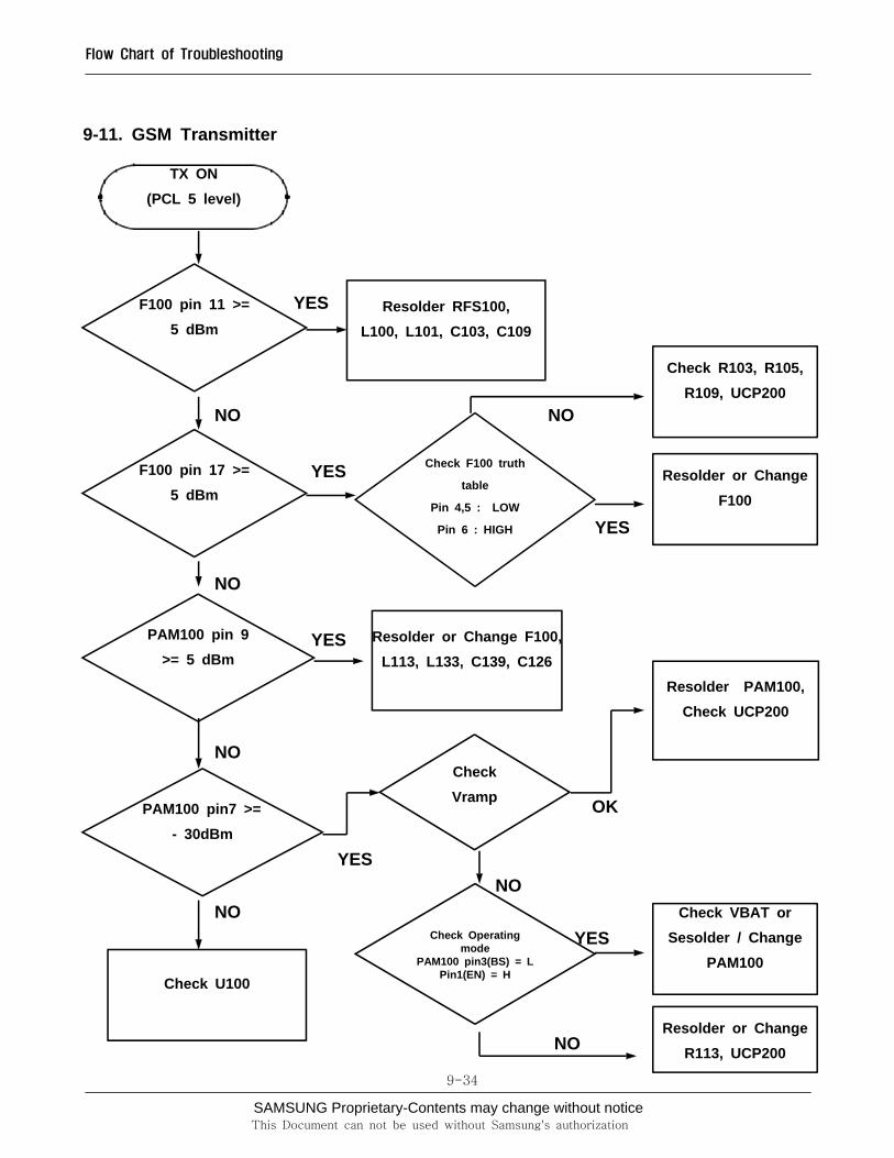
9-11. GSM Transmitter
YES
NO NO
YES
YES
NO
YES
NO
OK
YESNO
NOYES
NO
TX ON(PCL 5 level)
F100 pin 11 >=5 dBm
F100 pin 17 >=5 dBm
PAM100 pin 9>= 5 dBm
PAM100 pin7 >=- 30dBm
Check U100
Resolder or Change F100,L113, L133, C139, C126
Resolder RFS100,L100, L101, C103, C109
Check F100 truth
table
Pin 4,5 : LOW
Pin 6 : HIGH
Check Operatingmode
PAM100 pin3(BS) = LPin1(EN) = H
CheckVramp
Check R103, R105,R109, UCP200
Resolder or ChangeF100
Resolder PAM100,Check UCP200
Check VBAT orSesolder / Change
PAM100
Resolder or ChangeR113, UCP200
SAMSUNG Proprietary-Contents may change without notice
Flow Chart of Troubleshooting
9-35
This Document can not be used without Samsung's authorization
SAMSUNG Proprietary-Contents may change without notice
Flow Chart of Troubleshooting
9-36
This Document can not be used without Samsung's authorization
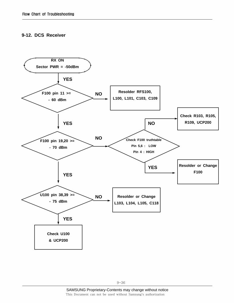
9-12. DCS Receiver
YES
NO
YES NO
NO
YESYES
NO
YES
RX ONSector PWR = -50dBm
F100 pin 11 >=- 60 dBm
Resolder RFS100,L100, L101, C103, C109
Check R103, R105,R109, UCP200
Check F100 truthtable
Pin 5,6 : LOW
Pin 4 : HIGH
F100 pin 19,20 >=- 70 dBm
Resolder or ChangeF100
U100 pin 38,39 >=- 75 dBm
Resolder or ChangeL103, L104, L105, C118
Check U100& UCP200
SAMSUNG Proprietary-Contents may change without notice
Flow Chart of Troubleshooting
9-37
This Document can not be used without Samsung's authorization

SAMSUNG Proprietary-Contents may change without notice
Flow Chart of Troubleshooting
9-38
This Document can not be used without Samsung's authorization
9-13. DCS Transmitter
YES
NO NO
YES
YES
NO
YES
NO
OK
YESNO
NOYES
NO
F100 pin 11 >=0 dBm
Resolder RFS100,L100, L101, C103, C109
Check R103, R105,R109, UCP200
Check F100 truth
table
Pin 4 : LOW
Pin 5,6 : HIGH
F100 pin 15 >=0 dBm Resolder or Change
F100
PAM100 pin 16>= 0 dBm
Resolder or Change F100,L114, C129, C140, C127
Resolder PAM100,Check UCP200
CheckVramp
Check Operating
mode
PAM100 pin3(BS) = H
Pin1(EN) = H
PAM100 pin2 >=- 25dBm
Check VBAT orSesolder / Change
PAM100
Resolder or ChangeR113, UCP200
Check U100
TX ON(PCL 0 level)

SAMSUNG Proprietary-Contents may change without notice
Flow Chart of Troubleshooting
9-39
This Document can not be used without Samsung's authorization

SAMSUNG Proprietary-Contents may change without notice
Flow Chart of Troubleshooting
9-40
This Document can not be used without Samsung's authorization
9-14. PCS Receiver
YES
NO
YES NO
NO
YESYES
NO
YES
RX ONSector PWR = -50dBm
F100 pin 11 >=- 60 dBm
Resolder RFS100,L100, L101, C103, C109
Check R103, R105,R109, UCP200
Check F100 truthtable
Pin 6 : LOW
Pin 4,5 : HIGH
F100 pin 21,22 >=- 70 dBm
Resolder or ChangeF100
U100 pin 38,39 >=- 75 dBm
Resolder or ChangeL106, L107, L108, C124
Check U100& UCP200

SAMSUNG Proprietary-Contents may change without notice
Flow Chart of Troubleshooting
9-41
This Document can not be used without Samsung's authorization

SAMSUNG Proprietary-Contents may change without notice
Flow Chart of Troubleshooting
9-42
This Document can not be used without Samsung's authorization
9-15. PCS Transmitter
YES
NO NO
YES
YES
NO
YES
NO
OK
YESNO
NOYES
NO
TX ON(PCL 0 level)
F100 pin 11 >=0 dBm
Resolder RFS100,L100, L101, C103, C109
Check R103, R105,R109, UCP200
Check F100 truth
table
Pin 4 : LOW
Pin 5,6 : HIGH
F100 pin 15 >=0 dBm
Resolder or ChangeF100
PAM100 pin 16>= 0 dBm
Resolder or Change F100,L114, C129, C140, C127
Resolder PAM100,Check UCP200
CheckVramp
PAM100 pin2 >=- 25dBm
Check U100
Check Operating
mode
PAM100 pin3(BS) = H
Pin1(EN) = H
Check VBAT orSesolder / Change
PAM100
Resolder or ChangeR113, UCP200

SAMSUNG Proprietary-Contents may change without notice
Flow Chart of Troubleshooting
9-43
This Document can not be used without Samsung's authorization

SAMSUNG Proprietary-Contents may change without notice
Flow Chart of Troubleshooting
9-44
This Document can not be used without Samsung's authorization
9-16. WCDMA Receiver
YESNO
YES NONO
YESYES
NO
YES
NO
YESNO
YESNO
F100 pin 11 >= -65 dBm
F100 pin 9 >= -70 dBm
U100 pin34,35 >=- 75dBm
U100 pin29 >=- 75dBm
U100 pin26 >=- 75dBm
F107 pin 2 >=- 75 dBm
Check F100 truth table
Pin 5 : LOW
Pin 4,6 : HIGH
Resolder orChange F100
Resolder RFS100,L100, L101, C103, C109
Resolder or ChangeU100
Resolder or ChangeC184, R131
Resolder or ChangeF107, L122, L123, L125,
C173
Check R103, R105,R109, UCP200
Check F101, C137,CL112,C142, L116, C141, L117,
C138, L115
Check U100& UCP200
RX ONSector PWR =
-50dBm

SAMSUNG Proprietary-Contents may change without notice
Flow Chart of Troubleshooting
9-45
This Document can not be used without Samsung's authorization

SAMSUNG Proprietary-Contents may change without notice
Flow Chart of Troubleshooting
9-46
This Document can not be used without Samsung's authorization
9-17. WCDMA 2100 Transmitter
YESNO
YES NONO
YESYES
NO
YES
NO NO
YESNO
YESYES
NO
Resolder RFS100,L100, L101, C103, C109
F100 pin 11 >=10dBm
Check R103, R105,R109, UCP200
Check F100 truth table
Pin 5 : LOW
Pin 4,6 : HIGH
F100 pin 9 >= 8dBm
Resolder orChange F100
Resolder or ChangeF107, L122, L123, L125,
C173
F107 pin 1 >=5 dBm
Check UCP 200PAM101 pin8 >=- 15dBm
PAM101 pin8 >=- 30dBm
Resolder or ChangeF105, L124
F105 pin1 >=- 30dBm
Check U100& UCP200
Check PAM101pin 3 = Lpin 4 = Lpin 5 =H
Check UCP 200
Check VBAT orResolder or Change
PAM101
TX ONSector PWR =
23dBm

SAMSUNG Proprietary-Contents may change without notice
Flow Chart of Troubleshooting
9-47
This Document can not be used without Samsung's authorization

SAMSUNG Proprietary-Contents may change without notice
Flow Chart of Troubleshooting
9-48
This Document can not be used without Samsung's authorization

SAMSUNG Proprietary-Contents may change without notice
10. Reference data
10-1
This Document can not be used without Samsung's authorization
Reference Abbreviate
― ARFCN : Absolute Radio Frequency Channel Number― BGA : Ball Grid Array― DCS : Digital Communications System― DL : Downlink― EDR : Enhanced Data Rate― EFS : Embaded File System― EGSM : Enhanced Global System for Mobile Communications― FTP : File Transfer Protocol― HPSK : Hybrid Phase Shift Keying― HSDPA : High Speed Downlink Packet Access― Mcps : Mega-chips per second― MMS : Multimedia Messaging Service― MSK : Minimum Shift Keying― OBEX : OBject EXchange― PBA : Panel Board Assembly― PCS : Personal Communication System― PIM(S) : Personal Information Management (System)― QPSK : Quadrature Phase Shift Keying― RNDIS : Remote Network Driver Interface Specification― RSS : Received Signal Strength― SAW : Surface Acoustic Wave― SMS : Short Message Service― UL : Uplink― USB : Universal Serial Bus― WCDMA : Wideband Code Division Multiple Access
SAMSUNG Proprietary-Contents may change without notice
Reference data
10-2
This Document can not be used without Samsung's authorization
SAMSUNG Proprietary-Contents may change without notice
11. Disassembly and Assembly Instructions
11-1
This Document can not be used without Samsung's authorization
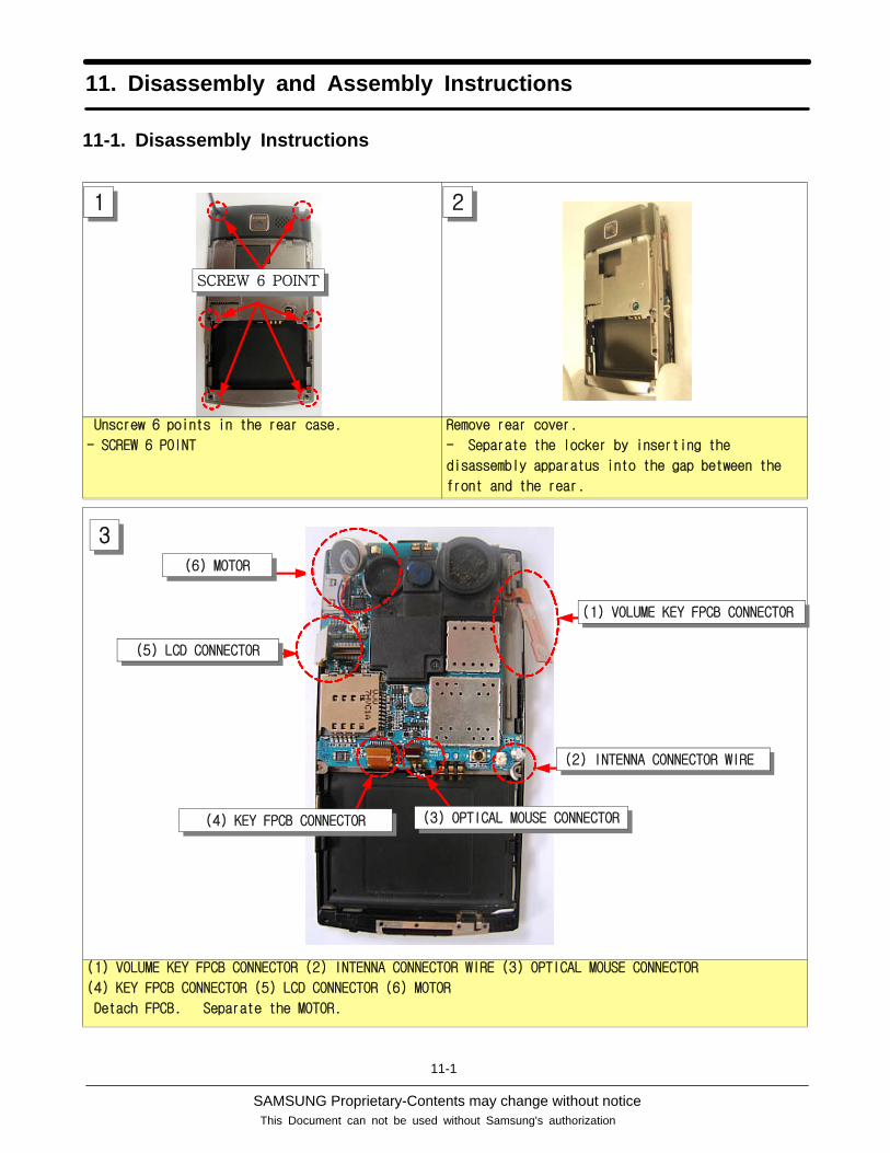
11-1. Disassembly Instructions
Unscrew 6 points in the rear case.
- SCREW 6 POINT
Remove rear cover.
- Separate the locker by inserting the
disassembly apparatus into the gap between the
front and the rear.
(1) VOLUME KEY FPCB CONNECTOR (2) INTENNA CONNECTOR WIRE (3) OPTICAL MOUSE CONNECTOR
(4) KEY FPCB CONNECTOR (5) LCD CONNECTOR (6) MOTOR
Detach FPCB. Separate the MOTOR.
21
SCREW 6 POINT
(6) MOTOR
(5) LCD CONNECTOR
(1) VOLUME KEY FPCB CONNECTOR
(4) KEY FPCB CONNECTOR (3) OPTICAL MOUSE CONNECTOR
(2) INTENNA CONNECTOR WIRE
3
SAMSUNG Proprietary-Contents may change without notice
Disassembly and Assembly Instructions
11-2
This Document can not be used without Samsung's authorization
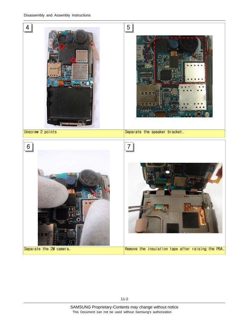
Unscrew 2 points Separate the speaker bracket.
Separate the 2M camera. Remove the insulation tape after raising the PBA.
54
76

SAMSUNG Proprietary-Contents may change without notice
Disassembly and Assembly Instructions
11-3
This Document can not be used without Samsung's authorization
Open the TSP WINDOW CONNECTOR LOCKER. Pick out the tsp window connector from the space
between LCD and PBA BRACKET.
꺼냄
Separate FRONT and PBA BRACKET ASS'Y. Separate RECEIVER and VGA CAMERA.
98
1110

SAMSUNG Proprietary-Contents may change without notice
Disassembly and Assembly Instructions
11-4
This Document can not be used without Samsung's authorization
Separate PBA BRACKET and PBA. Separate the VGA CAMERA after removing the
insulation tape.
Detach two SHIELD COVERS. Separate the MOTOR and SPEAKER after RE-
SOLDERING.
1312
1514

SAMSUNG Proprietary-Contents may change without notice
Disassembly and Assembly Instructions
11-5
This Document can not be used without Samsung's authorization
Separate the MOTOR and SPEAKER after
RESOLDERING.
Separate LCD and PBA BRACKET.
Separate PBA BRACKET and INTENNA WIRE. Remove the INTENNA.
Notice the MIC HOLDER.
1716
1918

SAMSUNG Proprietary-Contents may change without notice
Disassembly and Assembly Instructions
11-6
This Document can not be used without Samsung's authorization
11-2. Assembly Instructions
Attach KEY FPCB
1. Remove the sticker of the KEY FPCB.
2. Attach the KEY FPCB standardizing guide hole.
INTENNA ASSEMBLY
1. Press the intenna conector on intenna perpendicularly.
2. Attach INTENNA on PBA BRACKET.
Make sure the contact between GOLD GASKET andINTENNA CONNECTOR.
3. MIC HOLDER must be settled in INTENNA HOLE.
4. Attach the NTENNA CONNECTOR WIRE side of the PBA BRACKET. (refer to the picture)
1
2
< 1. INTENNA CONNECTOR 체결 >
< 4. INTENNA CONNECTOR WIRE 안착 >
< 2. GOLD GASKET과 INTENNA
CONNECTOR 접촉 확인 >
< 3. INTENNA ASSEMBLY >
SAMSUNG Proprietary-Contents may change without notice
Disassembly and Assembly Instructions
11-7
This Document can not be used without Samsung's authorization
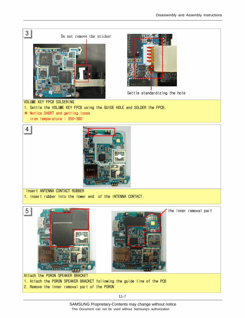
VOLUME KEY FPCB SOLDERING
1. Settle the VOLUME KEY FPCB using the GUIDE HOLE and SOLDER the FPCB.
※ Notice SHORT and getting loose
iron temperature : 350~380'
Insert ANTENNA CONTACT RUBBER
1. Insert rubber into the lower end of the INTENNA CONTACT.
Attach the PORON SPEAKER BRACKET
1. Attach the PORON SPEAKER BRACKET following the guide line of the PCB
2. Remove the inner removal part of the PORON
3Do not remove the sticker
Settle standardizing the hole
4
5 the inner removal part

SAMSUNG Proprietary-Contents may change without notice
Disassembly and Assembly Instructions
11-8
This Document can not be used without Samsung's authorization
Attach SHIELD COVER
1. Attach SHIELD COVER from the left side.
RECEIVER, MOTOR, SPEAKER SOLDERING
1. Solder the RECEIVER on the TOP side.
2. Solder the MOTOR and SPEAKER on the BOTTOM side.
※ Notice SHORT and getting loose
iron temperature : 350~380'
6
7
insert from the left side.notice the right insertion direction
RECEIVER SOLDERING MOTOR, SPEAKER SOLDERING

SAMSUNG Proprietary-Contents may change without notice
Disassembly and Assembly Instructions
11-9
This Document can not be used without Samsung's authorization
Attach CAMERAs
1. Inset the VGA CAMERA (standardize the FPCB SILK LINE) and attach the insulation tape after
closing the LOCKER.
2. Press the 2MEGA CAMERA.
Settle PBA / Attach the SPEAKER BRACKET
1. Inset the FPCB into the BRACKET.
2. Settle the PBA into the PBA BRACKET
3. Attach the MOTOR after assembling the SPEAKER BRACKET.
9
8 attach 2MEGA CAMERAattach VGA CAMERA
inset the FPCB into
the bracket FIRST.
attach
the MOTOR
notice
the
SPEAKER
settling
SAMSUNG Proprietary-Contents may change without notice
Disassembly and Assembly Instructions
11-10
This Document can not be used without Samsung's authorization
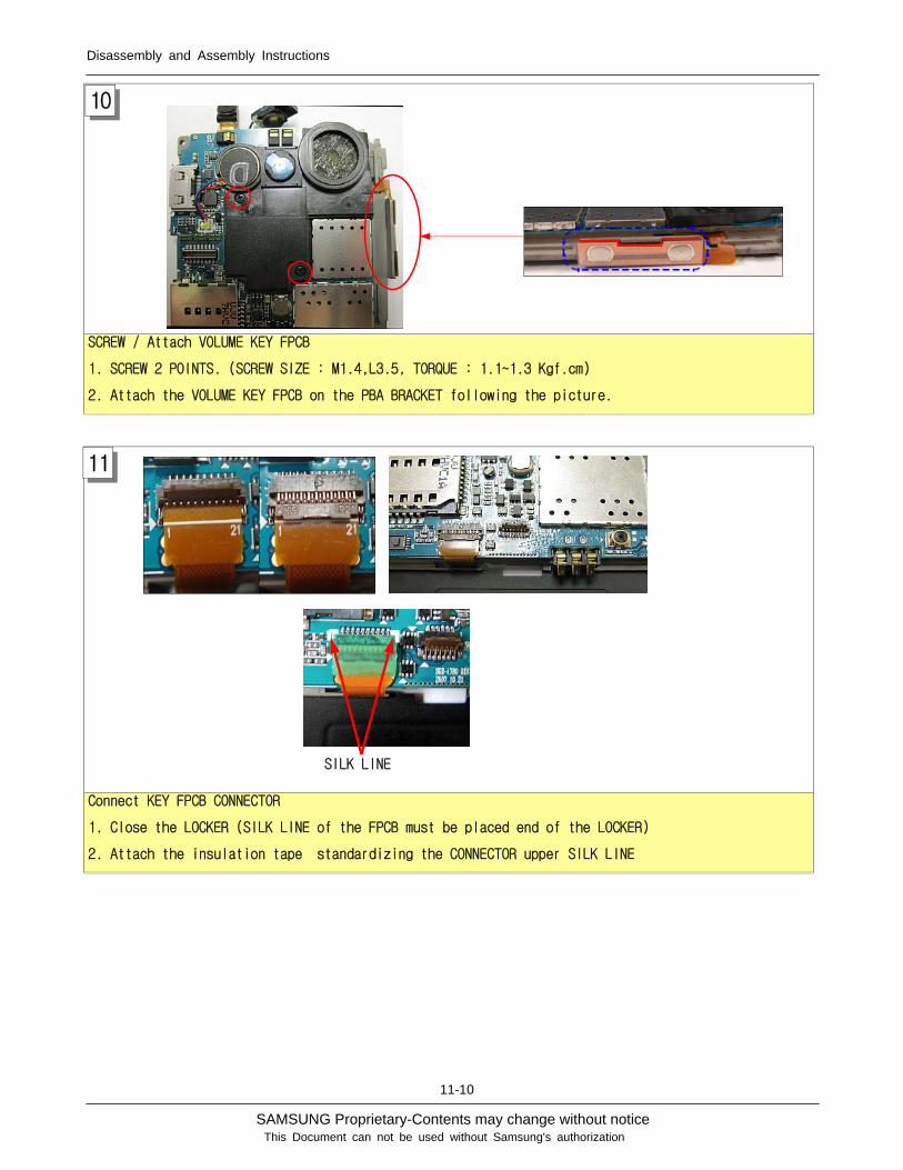
SCREW / Attach VOLUME KEY FPCB
1. SCREW 2 POINTS. (SCREW SIZE : M1.4,L3.5, TORQUE : 1.1~1.3 Kgf.cm)
2. Attach the VOLUME KEY FPCB on the PBA BRACKET following the picture.
Connect KEY FPCB CONNECTOR
1. Close the LOCKER (SILK LINE of the FPCB must be placed end of the LOCKER)
2. Attach the insulation tape standardizing the CONNECTOR upper SILK LINE
11
10
SILK LINE

SAMSUNG Proprietary-Contents may change without notice
Disassembly and Assembly Instructions
11-11
This Document can not be used without Samsung's authorization
Connect the INTENNA WIRE CONNECTOR / attach the RECEIVER and VGA CAMERA
1. Press the INTENNA WIRE CONNECTOR perpendicularly
2. Attach the RECEIVER and VGA CAMERA after removing stickers.
Attach the TSP WINDOW on FRONT
1. Remove the sticker of FRONT WINDOW
2. Insert TSP WINDOW FPCB CONNECTOR into the FRONT hole
3. Attach the TSP WINDOW on FRONT standardizing the upper line
12
13
remove sticker
attach after holding
attach the receiver standardizing left/lower-end RIB
insert TSP WINDOW
FPCB CONNECTOR into the FRONT hole
attach the TSP WINDOW on FRONT
standardizing the upper line

SAMSUNG Proprietary-Contents may change without notice
Disassembly and Assembly Instructions
11-12
This Document can not be used without Samsung's authorization
Settle LCD / Connect TSP WINDOW CONNECTOR
1. Settle LCD on FRONTstandardizing the upper line
2. Close the LOCKER (FPCB SILK LINE must be placed end of the LOCKER)
3. Attach the insulation tape standardizing the CONNECTOR lower end
KEY PAD
1. Settle the KEY PAD standardizing the HOOKER.
2. Make sure the key pad attachment.
14
15
standardizing the HOOKER
GUIDE PIN

SAMSUNG Proprietary-Contents may change without notice
Disassembly and Assembly Instructions
11-13
This Document can not be used without Samsung's authorization
OPTICAL MOUSE
1. Inset the OPTICAL MOUSE FPCB into the BRACKET hole
2. Close the LOCKER after inserting the CONNECTOR
3. Attach the insulation tape standardizing the CONNECTOR upper side.
Put the PBA BRACKET ASS'Y on FRONT
1. Put the PBA BRACKET ASS'Y on FRONT (right / upper side FIRST)
Notice interference between VOLUME KEY FPCB and FRONT RIB
2. Connect LCD CONNECTOR
17
16
inset the OPTICAL MOUSE FPCB
into the BRACKET holestandardizing the SILK LINE
attach the insulation tape
standardizing the CONNECTOR upper side.
notice interference between
VOLUME KEY FPCB and FRONT RIB
notice interference between
VOLUME KEY FPCB and FRONT RIBconnect the LCD CONNECTOR
SAMSUNG Proprietary-Contents may change without notice
Disassembly and Assembly Instructions
11-14
This Document can not be used without Samsung's authorization
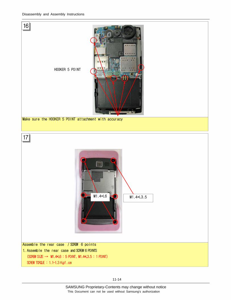
Make sure the HOOKER 5 POINT attachment with accuracy
Assemble the rear case / SCREW 6 points
1. Assemble the rear case and SCREW 6 POINTS
(SCREW SIZE → M1.4*L6 : 5 POINT, M1.4*L3.5 : 1 POINT)
SCREW TORQUE : 1.1~1.3 Kgf.cm
M1.4*L6 M1.4*L3.5
17
16
HOOKER 5 POINT