ripple carry adder design using universal logic … journal of engineering vol. 3(11), 1-5, november...
TRANSCRIPT

Research Journal of Engineering
Vol. 3(11), 1-5, November (201
International Science Congress Association
Ripple Carry Adder Design Using Universal Logic Gates
Department of ECE, Technocrats Institute of Technology, Bhopal, MP INDIA
AvailableReceived 25th September
Abstract
Now days a lot of refinements and huge amount of time is utilized on exploring layout to minimize the gate size or other
circuitry such as an memory element or adder in an integrated circuit (IC). In this research paper an analysis on power and
other parameters of Ripple Carry adder which is designed using UNIVERSAL GATES is discussed. And here layout design
and simulation is done with the help of Microwind and DSCH tool.
Keywords: Full Adder, Ripple Carry Adder (RCA), Power, Simulation
Introduction
Adder is basically a circuit used in digital arithmetic for
addition of two numbers which can be designed with the help of
CMOS16
. And in today’s scenario trend of CMOS
(Complementary Symmetry Metal Oxide
technology improvement continues to be driven with the need of
integrating more functions within given silicon area that is
single chip in order to increase operating speed, to reduce the
cost and less power consumption. Past few years it is
there is tremendous use of nano-scale technologies for industrial
production of high performance integrated circuits(IC) and the
two important characteristics of CMOS devices which are very
important are noise immunity and low static power
consumption. So many researchers are working in this field to
achieve such goals1, 2, 3, 4, 5
.
Here Microwind and DSCH software or tool is used (which is
basically a CMOS circuit editor and simulation tool) for logic
and layout-level design which was developed
In this paper, a Ripple Carry Adder based on NAND and NOR
logic gate layout is designed using Microwind as they are
helpful in designing of multiplier and many other things. So
firstly we design all the individual components and then further
their alignment and connected is done properly.
Material and Methods
Firstly here Full Adder design is discussed which is the basic
component in designing of ripple carry adder
Basic Full adder: A full adder circuit is basically used for
adding and consist of An, Bn and Cn-1 where
nth order bits of the numbers A and B respectively and
the carry generated from the addition of (
also has C (CI) as carry input, Co (carry/out2) as carry output
and S (out1/SUM) as Sum.
Engineering Sciences _______________________________
(2014)
Association
Ripple Carry Adder Design Using Universal Logic GatesPatel Chandrahash and C.S. Veena
Department of ECE, Technocrats Institute of Technology, Bhopal, MP INDIA
Available online at: www.isca.in, www.isca.me September 2014, revised 28th October 2014, accepted 20th November
Now days a lot of refinements and huge amount of time is utilized on exploring layout to minimize the gate size or other
circuitry such as an memory element or adder in an integrated circuit (IC). In this research paper an analysis on power and
rameters of Ripple Carry adder which is designed using UNIVERSAL GATES is discussed. And here layout design
and simulation is done with the help of Microwind and DSCH tool.
Full Adder, Ripple Carry Adder (RCA), Power, Simulation.
Adder is basically a circuit used in digital arithmetic for
addition of two numbers which can be designed with the help of
. And in today’s scenario trend of CMOS
xide Semiconductor)
technology improvement continues to be driven with the need of
integrating more functions within given silicon area that is
single chip in order to increase operating speed, to reduce the
cost and less power consumption. Past few years it is seen that
scale technologies for industrial
production of high performance integrated circuits(IC) and the
two important characteristics of CMOS devices which are very
important are noise immunity and low static power
So many researchers are working in this field to
Here Microwind and DSCH software or tool is used (which is
basically a CMOS circuit editor and simulation tool) for logic
level design which was developed since 19986.
In this paper, a Ripple Carry Adder based on NAND and NOR
logic gate layout is designed using Microwind as they are
helpful in designing of multiplier and many other things. So
firstly we design all the individual components and then further
their alignment and connected is done properly.
Firstly here Full Adder design is discussed which is the basic
component in designing of ripple carry adder
A full adder circuit is basically used for
where An and Bn are the
respectively and Cn-1 is
the carry generated from the addition of (n-1)th order bits and
ry input, Co (carry/out2) as carry output
Tables 1 show the truth table and figure 1(a
and symbol of a 1-bit full adder.
Figure
(a) Logic and (b) Block Diagram of 1
__________________ ISSN 2278 – 9472
Res. J. Engineering Sci.
1
Ripple Carry Adder Design Using Universal Logic Gates
Department of ECE, Technocrats Institute of Technology, Bhopal, MP INDIA
November 2014
Now days a lot of refinements and huge amount of time is utilized on exploring layout to minimize the gate size or other
circuitry such as an memory element or adder in an integrated circuit (IC). In this research paper an analysis on power and
rameters of Ripple Carry adder which is designed using UNIVERSAL GATES is discussed. And here layout design
Tables 1 show the truth table and figure 1(a-b) shows the logic
bit full adder.
(a)
(b)
Figure-1
(b) Block Diagram of 1-bit basic Full Adder
Research Journal of Engineering Sciences
Vol. 3(11), 1-5, November (2014)
International Science Congress Association
Table-1
Truth Table of 1-bit basic Full Adder
Input Bit
for
Number Carry
Input(C/CI)
Sum bit
Output(S)
A B
0 0 0 0
0 0 1 1
0 1 0 1
0 1 1 0
1 0 0 1
1 0 1 0
1 1 0 0
1 1 1 1
Ripple Carry adder: Logical circuit with multiple full adders
can be used for adding N-bit numbers and each full adder inputs
a Cin, which is the Cout of the previous adder. Such kind of
adder is known as Ripple Carry Adder, since each carry bit
"ripples" to the next full adder
Figure-2
Block Diagram of 4-Bit Ripple Carry Adder
So ripple carry adder in digital electronics is that circuit which
produces the arithmetic sum of two binary numbers which can
be constructed with full adders connected in cascaded with the
carry output from each full adder connected to the carry input of
the next full adder in the chain as shown in figure 2. From
which it can be noticed that bits a0and b0 in the figure represent
the least significant bits of the numbers which is to be added
and sum in form of output represented by the bits s0
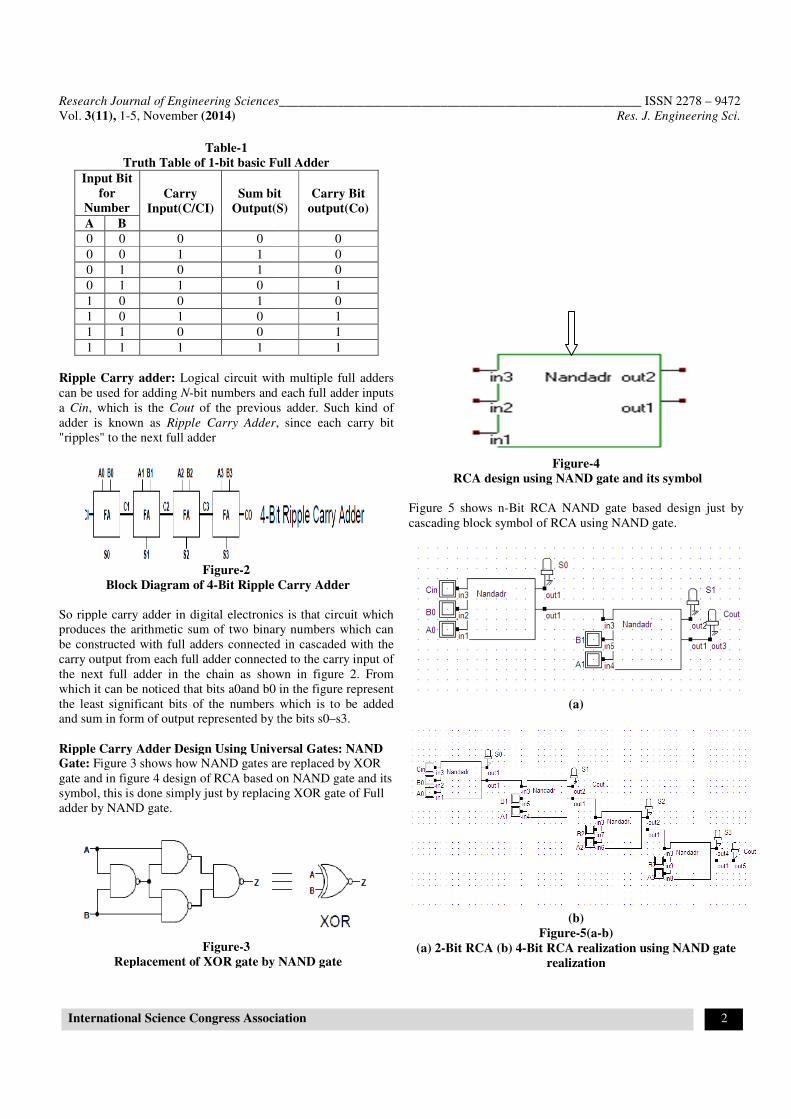
Ripple Carry Adder Design Using Universal Gates: NAND
Gate: Figure 3 shows how NAND gates are replaced by XOR
gate and in figure 4 design of RCA based on NAND gate and its
symbol, this is done simply just by replacing XOR gate of Full
adder by NAND gate.
Figure-3
Replacement of XOR gate by NAND gate
Sciences___________________________________________
Association
bit basic Full Adder
Sum bit
Output(S)
Carry Bit
output(Co)
0
0
0
1
0
1
1
1
Logical circuit with multiple full adders
bit numbers and each full adder inputs
of the previous adder. Such kind of
, since each carry bit
Bit Ripple Carry Adder
ripple carry adder in digital electronics is that circuit which
produces the arithmetic sum of two binary numbers which can
be constructed with full adders connected in cascaded with the
output from each full adder connected to the carry input of
the next full adder in the chain as shown in figure 2. From
which it can be noticed that bits a0and b0 in the figure represent
the least significant bits of the numbers which is to be added
m in form of output represented by the bits s0–s3.
Ripple Carry Adder Design Using Universal Gates: NAND
Figure 3 shows how NAND gates are replaced by XOR
gate and in figure 4 design of RCA based on NAND gate and its
by replacing XOR gate of Full
Replacement of XOR gate by NAND gate
Figure
RCA design using NAND gate and its symbol
Figure 5 shows n-Bit RCA NAND gate based design just by
cascading block symbol of RCA using
Figure
(a) 2-Bit RCA (b) 4-Bit RCA realization using NAND gate
realization
_______________________________ ISSN 2278 – 9472
Res. J. Engineering Sci.
2
Figure-4
RCA design using NAND gate and its symbol
Bit RCA NAND gate based design just by
cascading block symbol of RCA using NAND gate.
(a)
(b)
Figure-5(a-b)
Bit RCA realization using NAND gate
realization
Research Journal of Engineering Sciences
Vol. 3(11), 1-5, November (2014)
International Science Congress Association
Figure-6 shows the layout diagram designed under Microwind
tool/ software.
Figure-6
Layout Diagram of NAND gate based RCA
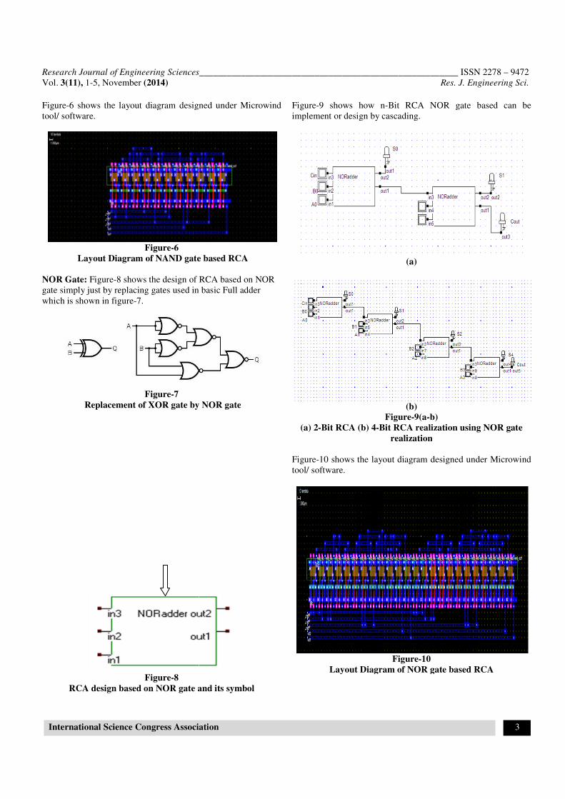
NOR Gate: Figure-8 shows the design of RCA based on NOR
gate simply just by replacing gates used in basic Full adder
which is shown in figure-7.
Figure-7
Replacement of XOR gate by NOR gate
Figure-8
RCA design based on NOR gate and its symbol
Sciences___________________________________________
Association
6 shows the layout diagram designed under Microwind
Layout Diagram of NAND gate based RCA
shows the design of RCA based on NOR
gate simply just by replacing gates used in basic Full adder
Replacement of XOR gate by NOR gate
RCA design based on NOR gate and its symbol
Figure-9 shows how n-Bit RCA NOR gate based can be
implement or design by cascading.
Figure
(a) 2-Bit RCA (b) 4-Bit RCA realization using NOR gate
realization
Figure-10 shows the layout diagram designed under Microwind
tool/ software.
Figure
Layout Diagram of NOR gate based RCA
_______________________________ ISSN 2278 – 9472
Res. J. Engineering Sci.
3
Bit RCA NOR gate based can be
implement or design by cascading.
(a)
(b)
Figure-9(a-b)
Bit RCA realization using NOR gate
realization
10 shows the layout diagram designed under Microwind
Figure-10
Layout Diagram of NOR gate based RCA

Research Journal of Engineering Sciences
Vol. 3(11), 1-5, November (2014)
International Science Congress Association
Results and Discussion
As CMOS logic dissipates less power than any other logic
circuits since it talk about switching power (dynamic power)
only. So Here power consumption and the number of routed
wires of NAND and NOR based RCA Adder are displayed in
table 2 as shown below. These results are obtained under
Microwind software and designing is done under DSCH tool
which is a part of Microwind software.
Table-2
Comparison of RCA design using Universal Gates
Universal gates NAND
Number of Routed wires 24
Area(µm2) 577.7
Power(mW) 0.105
(a)
(b)
Figure-11
Graphical Presentation of (a) Power and (b) Area and
Number of routing wires
of NAND and NOR gate based RCA
Conclusion
In this paper a compact and basic 4 –bit
designed using NAND and NOR gates (universal gates) which is
shown with their design topology, detailed
ease of verification. H e r e w h i l e designing
(that is gate level approach) i s u s e d
universal gate a r e used and found NAND
proved to be more efficient than NOR gate
other types of adders as Carry Select adder, Carry Skip Adder,
Carry look ahead adder etc. require more area than t
carry adder. That’s why there is always a scope to trade off
0
0.05
0.1
0.15
0.2
0.25
NAND NOR
0
500
1000
1500
Sciences___________________________________________
Association
As CMOS logic dissipates less power than any other logic
circuits since it talk about switching power (dynamic power)
only. So Here power consumption and the number of routed
R based RCA Adder are displayed in
table 2 as shown below. These results are obtained under
Microwind software and designing is done under DSCH tool
Comparison of RCA design using Universal Gates
NOR
26
1298.1
0.232
Graphical Presentation of (a) Power and (b) Area and
Number of routing wires
of NAND and NOR gate based RCA
bit Ripple Carry Adder
gates (universal gates) which is
topology, detailed analysis and i t s
designing basic approach
i s u s e d and f o r t h a t
used and found NAND gate based design
gate based design. While
other types of adders as Carry Select adder, Carry Skip Adder,
Carry look ahead adder etc. require more area than the ripple
carry adder. That’s why there is always a scope to trade off
between the speed and the size of the device while designing
any adder circuit and can be used for various applications
Figure
Analog simulation of NAND
References
1. Rawwat K., Darwish T. and Bayoumi M., A low power
carry select adder with reduces area,
Symposium on Circuits and Systems
2. Tyagi A., A reduced area scheme for carry
IEEE Trans. on Computer,
3. Jeong W. and Roy K., Robust high
power adder, Proc. of the Asia and South Pacific Design
Automation Conference
4. Steven M. Nowick, Kenneth Y. Yun, Ayoob E. Dooply
and Peter A. Beerel, Specu
of high-performance asynchronous dynamic adders. In
Proceedings of the 3rd International Symposium on
Advanced Research in Asynchronous Circuits and
Systems, page 210, IEEE Computer Society,
5. Safi Seyyed Mohammad, Ras
Kaboli Mina and Safi Fatemeh Sadat, An Efficient
Residue to Binary Converter for the New Two
Moduli Set, Research Journal of Recent Sciences,
83-86, (2012)
POWER(mW)
Number of
Routed wires
Area(µm2)
_______________________________ ISSN 2278 – 9472
Res. J. Engineering Sci.
4
between the speed and the size of the device while designing
any adder circuit and can be used for various applications7- 10
.
(a)
(b)
Figure-12
Analog simulation of NAND and NOR gate based RCA
Rawwat K., Darwish T. and Bayoumi M., A low power
carry select adder with reduces area, Proc. of Midwest
Symposium on Circuits and Systems, 218-221, (2001)
Tyagi A., A reduced area scheme for carry-select adders,
on Computer, 42, 1163-1170, (1993)
Jeong W. and Roy K., Robust high-performance low
Proc. of the Asia and South Pacific Design
Automation Conference, 503-506, (2003)
Steven M. Nowick, Kenneth Y. Yun, Ayoob E. Dooply
and Peter A. Beerel, Speculative completion for the design
performance asynchronous dynamic adders. In
3rd International Symposium on
Advanced Research in Asynchronous Circuits and
IEEE Computer Society, (1997)
Safi Seyyed Mohammad, Rashno Meysam, Abedi Parvin,
Kaboli Mina and Safi Fatemeh Sadat, An Efficient
Residue to Binary Converter for the New Two-Level
Research Journal of Recent Sciences, 1(7),
Research Journal of Engineering Sciences________________________________________________________ ISSN 2278 – 9472
Vol. 3(11), 1-5, November (2014) Res. J. Engineering Sci.
International Science Congress Association 5
6. Sicard, Ssfa; and S. M. Aziz, Microwind application notes
for 90-nm, 65-nm, 45-nm and 32-nm technologies,
http://www.microwind.org., (2014)
7. Sanjay, VHDL Environment for Floating point Arithmetic
Logic Unit- ALU design and simulation, Research J.
Engineering Sci., 1(2),1-6(2012)
8. Xiaochen Guo, Engin Ipek and Tolga Soyata, Resistive
Computation: Avoiding the Power Wall with Low-
Leakage, STT-MRAM Based Computing, ISCA'10, June
19–23, (2010)
9. Weste Neil H.E. and Eshraghian, Kamran. Principles of
CMOS VLSI Design, Third Edition, Addison Wesley,
(2004)
10. Sujata Verma S.K Singh and A.G. Rao, Overview of
Contro techniques for DC-Dc converters, Res. J.
Engineering Sci., 2(8),18-21(2013)
11. Kang Sung-Mo (Steve) and Leblebici, Yusuf. CMOS
Digital Integrated Circuits Analysis and Design, Third
Edition, McGraw-Hill, (2002)
12. Tocci, Ronald J. and S. Neal Widmer, Digital Systems:
Principles and Applications, 8th Edition, Prentice Hall,
(2001)
13. Weste Neil H.E. and M. David Harris, CMOS VLSI
Design: A Circuits and Systems Perspective, Fourth
Edition. Boston: Pearson/Addison-Wesley, (2010)
14. Kamal Raj, Digital Principles and Design, Chapter 6,
Pearson Education, (2006)