high performance ripple carry adder using domino logic · performance of 8-bit ripple carry adder...
TRANSCRIPT
International Research Journal of Engineering and Technology (IRJET) e-ISSN: 2395 -0056
Volume: 02 Issue: 08 | Nov-2015 www.irjet.net p-ISSN: 2395-0072
© 2015, IRJET ISO 9001:2008 Certified Journal Page 406
HIGH PERFORMANCE RIPPLE CARRY ADDER USING
DOMINO LOGIC
Dr.J.Karpagam1 , A.Arunadevi2
1 Professor, Department of ECE, KPRIET, Coimbatore, Tamilnadu, India 2 PG Scholar, Department of ECE, KPRIET, Coimbatore, Tamilnadu, India
---------------------------------------------------------------------***---------------------------------------------------------------------
ABSTRACT
The demand and popularity of portable electronics is driving designers to strive for small silicon area, higher speeds, low power dissipation and reliability. Domino logic circuits are important as it provides better speed and has lesser transistor requirement when compared to static CMOS logic circuits. This project presents the design and performance of 8-bit Ripple Carry Adder using CMOS
Domino logic targeting at full-custom high speed applications. The constant delay characteristic of this logic style regardless of the logic expression makes it suitable for
implementing complicated logic expression such as addition. This feature enables performance advantage over static and dynamic, CD logic styles in a single cycle, multi-stage circuit block. Post layout simulation results of 8-bit ripple carry adders conclude that the proposed circuit has very low
power consumption and lesser delay compared to the recently proposed circuit techniques.
Keywords: Domino Logic Circuits, Ripple Carry Adder, Constant Delay, Post Layout Simulation, CD Logic.
1. INTRODUCTION
Eventhough the static CMOS logic offers less speed, it is best known for its lowest power dissipation. As the number of inputs increase, the number of transistors required will be doubled. In order to reduce the transistor count, pseudo NMOS is preferred, then area is also reduced. But it fails to improve speed and reduce power dissipation. The nominal low output voltage for Pseudo NMOS is not 0V since, there is a fight between the devices in the pull down network and the grounded PMOS load device. This results in reduced noise margins and more importantly static power dissipation. Dynamic logic is well suited for high speed circuit design as it requires less number of transistors to implement a given logic, but the major drawback with this logic is its excessive power dissipation due to the switching activity and clock. The power dissipation of dynamic logic circuit is reduced
excessively with a mixer of dynamic and static circuit styles, use of dual supply voltages and dual threshold voltages.
Domino logic is a clocked logic family which means that every single logic gate has a clock signal present. When the clock signal turns low, node N0 goes high, causing the output of the gate to go low. This represents the only mechanism for the gate output to go low once it has been driven high. The operating period of the cell when its input clock and output are low is called the recharge phase or cycle. The next phase, when the clock is high, is called the evaluate phase or cycle. The evaluate phase is the functional operating phase in domino cells, with the recharge phase enabling the next evaluate phase to occur. The appropriate application of the clock signal ensures that the critical path in domino cells only traverses through cells in the evaluate phase. Since the domino cell only switches from a low to a high direction, there is no need for the inputs to drive any pull-up PMOS transistors. The lack of a PMOS transistor means that the effective transistor width that loads down a previous stage of logic, for a particular current drive, favors domino over static logic. This is critical since the key to high speed ensures
that a speed advantage can be gained without loading down the cell greatly.
Continuous scaling of the transistor size and reduction of the operating voltage has led to a significant performance improvement of integrated circuits. Low power consumption and smaller area are some of the most important criteria for the fabrication of DSP systems and high performance systems. The adder is the most commonly used arithmetic block of the Central Processing Unit (CPU) and Digital Signal Processing (DSP), therefore its performance and power optimization is of utmost importance. With the technology scaling to deep sub- micron, the speed of the circuit increases rapidly. At the same time, the power consumption per chip also increases significantly due to the increasing density of the chip. Therefore, in realizing Modern Very Large Scale Integration (VLSI) circuits, low-power and high-speed are the two predominant factors which need to be considered. Like any other circuit design, the design of high- performance and low-power adders can be addressed at
International Research Journal of Engineering and Technology (IRJET) e-ISSN: 2395 -0056
Volume: 02 Issue: 08 | Nov-2015 www.irjet.net p-ISSN: 2395-0072
© 2015, IRJET ISO 9001:2008 Certified Journal Page 407
different levels, such as architecture, logic style, layout, and the process technology. The carry-ripple adder is composed of many cascaded single-bit full-adders. The circuit architecture is simple and area-efficient. However, the computation speed is slow because each full-adder can only start operation till the previous carry-out signal is ready.
2. LOGIC DESIGNS
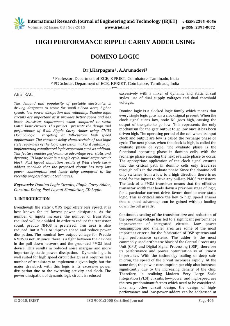
2.1 Static Logic
Static logic is the most widely used logic style in CMOS technology and its basic structure as shown in Figure 1. It consists of a NMOS pull-down network (PDN) and a PMOS pull-up network (PUN). The primary advantages of static logic are robustness, low power dissipation especially at low data activity factor, and adequate performance with no static power dissipation. Its most distinct characteristic is that at any given time, the gate output is connected to either VDD or GND via a low-resistance path.
Fig-1: Static Logic
While this unique feature ensures static logic's robustness, it is also a major drawback since static CMOS requires both NMOS and PMOS transistors on each input. During a falling output transition, PMOS transistors do not contribute to the pull-down transition current but only add significant capacitance. Hence, static CMOS has a relatively large logical effort and area penalty and is slow when implementing complicated logic expression such as 4-input XOR. The PDN and PUN are implemented using NMOS and PMOS devices because they can pass strong logic “0" and “1" respectively. PMOS devices are typically sized up two times larger than NMOS devices to provide equal rise and fall delay due to lower whole mobility. Therefore, PMOS transistors have to be up sized four times larger than NMOS transistors to achieve equivalent rise and fall delay for the two-input NOR gate. The up-sized PMOS transistors contribute input capacitance for both transitions, while only helping the rise delay. In this regard, PMOS devices neither become the area bottleneck for static CMOS logic style when implementing NOR gate
(PMOS devices in series). Furthermore, the up-sizing technique provides diminished rising delay improvement due to self-loading effect; since the additional drain capacitance introduced by up-sizing gradually offsets the performance enhancement contributed by higher pull-up current as a result of larger width device.
2.2 Dynamic & Compound Domino Logic
The invention of the dynamic logic in the 80s is one of the answers to the request of ever increasing IC operating speed as it allows designers to implement high performance circuit block, i.e., arithmetic logic unit (ALU), at an operating frequency that the traditional static and pass transistor CMOS logic styles are difficult to achieve.
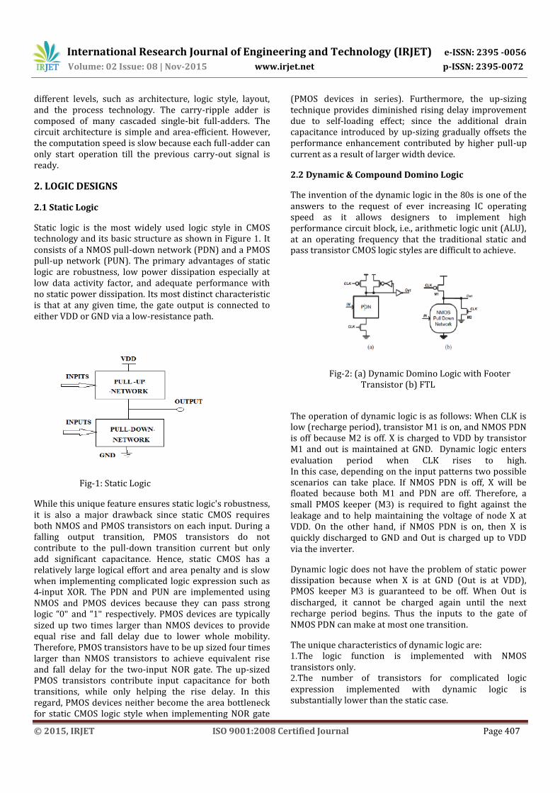
Fig-2: (a) Dynamic Domino Logic with Footer Transistor (b) FTL
The operation of dynamic logic is as follows: When CLK is low (recharge period), transistor M1 is on, and NMOS PDN is off because M2 is off. X is charged to VDD by transistor M1 and out is maintained at GND. Dynamic logic enters evaluation period when CLK rises to high. In this case, depending on the input patterns two possible scenarios can take place. If NMOS PDN is off, X will be floated because both M1 and PDN are off. Therefore, a small PMOS keeper (M3) is required to fight against the leakage and to help maintaining the voltage of node X at VDD. On the other hand, if NMOS PDN is on, then X is quickly discharged to GND and Out is charged up to VDD via the inverter.
Dynamic logic does not have the problem of static power dissipation because when X is at GND (Out is at VDD), PMOS keeper M3 is guaranteed to be off. When Out is discharged, it cannot be charged again until the next recharge period begins. Thus the inputs to the gate of NMOS PDN can make at most one transition.
The unique characteristics of dynamic logic are: 1.The logic function is implemented with NMOS transistors only. 2.The number of transistors for complicated logic expression implemented with dynamic logic is substantially lower than the static case.
International Research Journal of Engineering and Technology (IRJET) e-ISSN: 2395 -0056
Volume: 02 Issue: 08 | Nov-2015 www.irjet.net p-ISSN: 2395-0072
© 2015, IRJET ISO 9001:2008 Certified Journal Page 408
3.Dynamic logic has faster switching speed because less number of transistors (especially without any PMOS logic transistors) contributes to less load capacitance. 4.It only consumes dynamic power since no static current path ever exists between VDD and GND.
However, the overall power consumption can be significantly higher than the static design because of the higher switching activity. The performance enhancement comes with several costs however, including reduced noise margin, charge- sharing noise, and higher power dissipation due to higher data activity. In a traditional dynamic logic, an output inverter is required between dynamic logics to satisfy the data monotonicity requirement and to ensure proper logic evaluation. This not only increases the overall delay but also the power consumption as well.
Two variations of the dynamic logic have been proposed to mitigate this problem. NP domino, or also known as NORA domino, replaces this inverter with pre- discharged dynamic gates using PMOS logic. However, NORA is extremely susceptible to noise and has not been used extensively. Zipper domino attempts to achieve the same objective by a slightly different implementation, but is never widespread in the VLSI industry. Furthermore, dynamic logic has gradually lost its performance advantage over static logic due to the increased self-loading ratio in deep-submicron technology (65nm and below) because of the additional NMOS CLK footer transistor (Figure 2(b)). This phenomena has been demonstrated in , which concludes that at processes such as 180nm and 130nm, the optimal adder architecture is radix-4 (5 transistors in series, including the footer transistor); however, radix-2 (3 transistors in series, including the footer transistor) con_guration becomes optimal at 65nm technology and beyond because the increased self-loading ratio has made radix-4 architecture slower than radix-2, even though radix-2 configuration requires more number of stages to complete the addition.
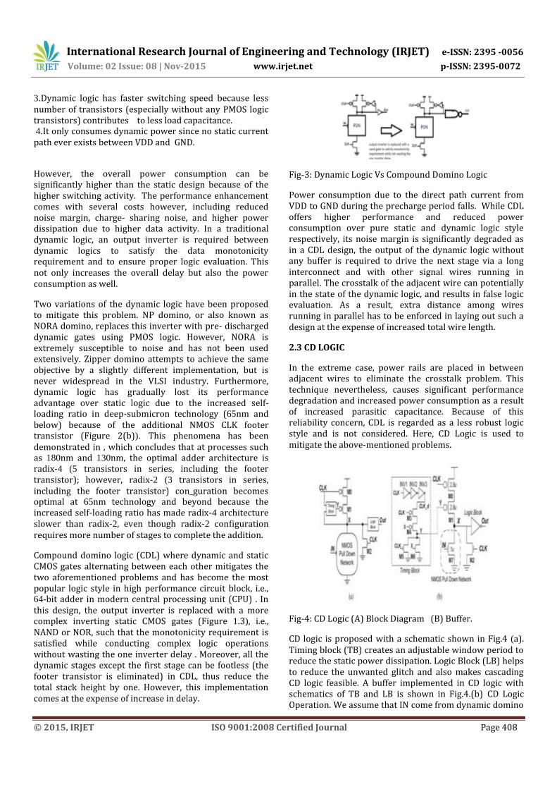
Compound domino logic (CDL) where dynamic and static CMOS gates alternating between each other mitigates the two aforementioned problems and has become the most popular logic style in high performance circuit block, i.e., 64-bit adder in modern central processing unit (CPU) . In this design, the output inverter is replaced with a more complex inverting static CMOS gates (Figure 1.3), i.e., NAND or NOR, such that the monotonicity requirement is satisfied while conducting complex logic operations without wasting the one inverter delay . Moreover, all the dynamic stages except the first stage can be footless (the footer transistor is eliminated) in CDL, thus reduce the total stack height by one. However, this implementation comes at the expense of increase in delay.
Fig-3: Dynamic Logic Vs Compound Domino Logic
Power consumption due to the direct path current from VDD to GND during the precharge period falls. While CDL offers higher performance and reduced power consumption over pure static and dynamic logic style respectively, its noise margin is significantly degraded as in a CDL design, the output of the dynamic logic without any buffer is required to drive the next stage via a long interconnect and with other signal wires running in parallel. The crosstalk of the adjacent wire can potentially in the state of the dynamic logic, and results in false logic evaluation. As a result, extra distance among wires running in parallel has to be enforced in laying out such a design at the expense of increased total wire length.
2.3 CD LOGIC
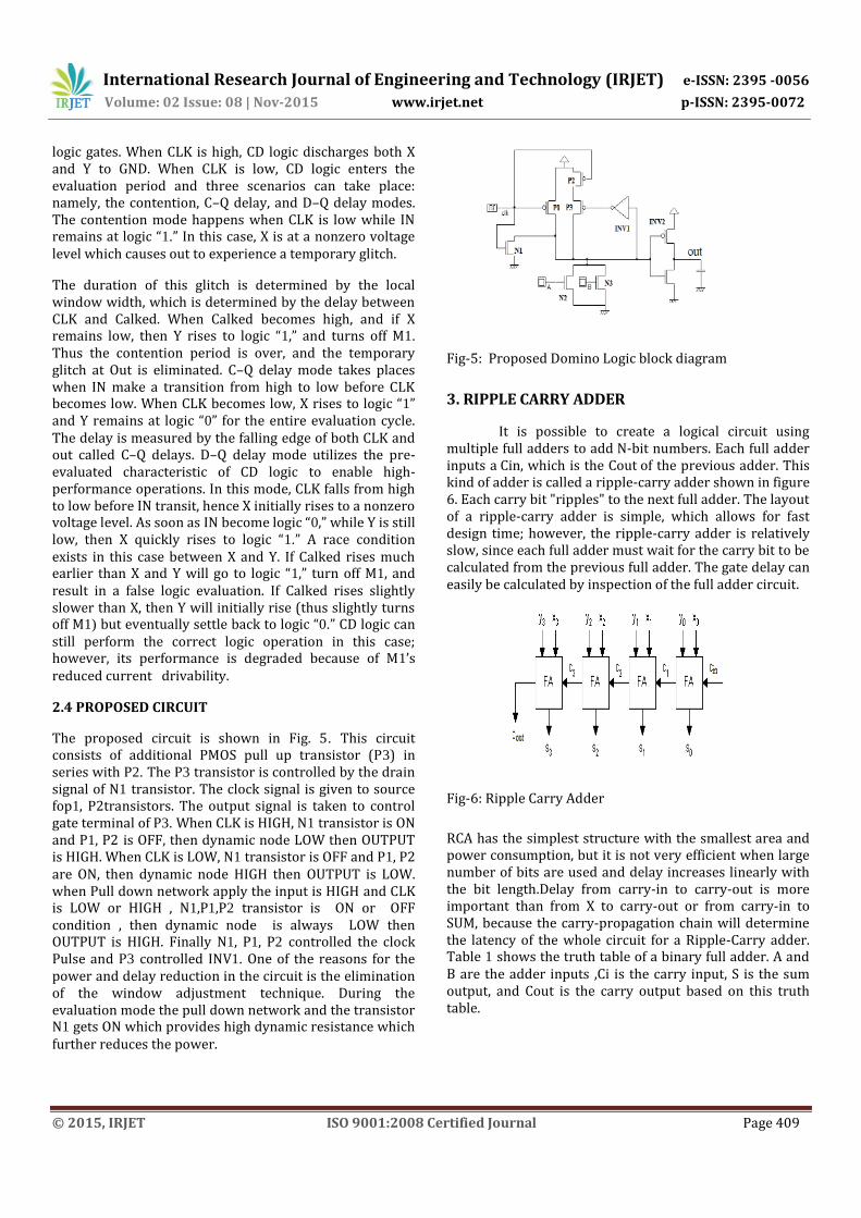
In the extreme case, power rails are placed in between adjacent wires to eliminate the crosstalk problem. This technique nevertheless, causes significant performance degradation and increased power consumption as a result of increased parasitic capacitance. Because of this reliability concern, CDL is regarded as a less robust logic style and is not considered. Here, CD Logic is used to mitigate the above-mentioned problems.
Fig-4: CD Logic (A) Block Diagram (B) Buffer.
CD logic is proposed with a schematic shown in Fig.4 (a). Timing block (TB) creates an adjustable window period to reduce the static power dissipation. Logic Block (LB) helps to reduce the unwanted glitch and also makes cascading CD logic feasible. A buffer implemented in CD logic with schematics of TB and LB is shown in Fig.4.(b) CD Logic Operation. We assume that IN come from dynamic domino
International Research Journal of Engineering and Technology (IRJET) e-ISSN: 2395 -0056
Volume: 02 Issue: 08 | Nov-2015 www.irjet.net p-ISSN: 2395-0072
© 2015, IRJET ISO 9001:2008 Certified Journal Page 409
logic gates. When CLK is high, CD logic discharges both X and Y to GND. When CLK is low, CD logic enters the evaluation period and three scenarios can take place: namely, the contention, C–Q delay, and D–Q delay modes. The contention mode happens when CLK is low while IN remains at logic “1.” In this case, X is at a nonzero voltage level which causes out to experience a temporary glitch.
The duration of this glitch is determined by the local window width, which is determined by the delay between CLK and Calked. When Calked becomes high, and if X remains low, then Y rises to logic “1,” and turns off M1.
Thus the contention period is over, and the temporary glitch at Out is eliminated. C–Q delay mode takes places when IN make a transition from high to low before CLK becomes low. When CLK becomes low, X rises to logic “1” and Y remains at logic “0” for the entire evaluation cycle. The delay is measured by the falling edge of both CLK and out called C–Q delays. D–Q delay mode utilizes the pre-evaluated characteristic of CD logic to enable high-performance operations. In this mode, CLK falls from high to low before IN transit, hence X initially rises to a nonzero voltage level. As soon as IN become logic “0,” while Y is still low, then X quickly rises to logic “1.” A race condition exists in this case between X and Y. If Calked rises much earlier than X and Y will go to logic “1,” turn off M1, and result in a false logic evaluation. If Calked rises slightly slower than X, then Y will initially rise (thus slightly turns off M1) but eventually settle back to logic “0.” CD logic can still perform the correct logic operation in this case; however, its performance is degraded because of M1’s reduced current drivability.
2.4 PROPOSED CIRCUIT
The proposed circuit is shown in Fig. 5. This circuit consists of additional PMOS pull up transistor (P3) in series with P2. The P3 transistor is controlled by the drain signal of N1 transistor. The clock signal is given to source fop1, P2transistors. The output signal is taken to control gate terminal of P3. When CLK is HIGH, N1 transistor is ON and P1, P2 is OFF, then dynamic node LOW then OUTPUT is HIGH. When CLK is LOW, N1 transistor is OFF and P1, P2
are ON, then dynamic node HIGH then OUTPUT is LOW. when Pull down network apply the input is HIGH and CLK is LOW or HIGH , N1,P1,P2 transistor is ON or OFF condition , then dynamic node is always LOW then OUTPUT is HIGH. Finally N1, P1, P2 controlled the clock Pulse and P3 controlled INV1. One of the reasons for the power and delay reduction in the circuit is the elimination of the window adjustment technique. During the evaluation mode the pull down network and the transistor N1 gets ON which provides high dynamic resistance which further reduces the power.
Fig-5: Proposed Domino Logic block diagram
3. RIPPLE CARRY ADDER
It is possible to create a logical circuit using multiple full adders to add N-bit numbers. Each full adder inputs a Cin, which is the Cout of the previous adder. This kind of adder is called a ripple-carry adder shown in figure 6. Each carry bit "ripples" to the next full adder. The layout of a ripple-carry adder is simple, which allows for fast design time; however, the ripple-carry adder is relatively slow, since each full adder must wait for the carry bit to be calculated from the previous full adder. The gate delay can easily be calculated by inspection of the full adder circuit.
Fig-6: Ripple Carry Adder
RCA has the simplest structure with the smallest area and power consumption, but it is not very efficient when large number of bits are used and delay increases linearly with the bit length.Delay from carry-in to carry-out is more important than from X to carry-out or from carry-in to SUM, because the carry-propagation chain will determine the latency of the whole circuit for a Ripple-Carry adder. Table 1 shows the truth table of a binary full adder. A and B are the adder inputs ,Ci is the carry input, S is the sum output, and Cout is the carry output based on this truth table.
International Research Journal of Engineering and Technology (IRJET) e-ISSN: 2395 -0056
Volume: 02 Issue: 08 | Nov-2015 www.irjet.net p-ISSN: 2395-0072
© 2015, IRJET ISO 9001:2008 Certified Journal Page 410
Table-1: Full Adder truth table
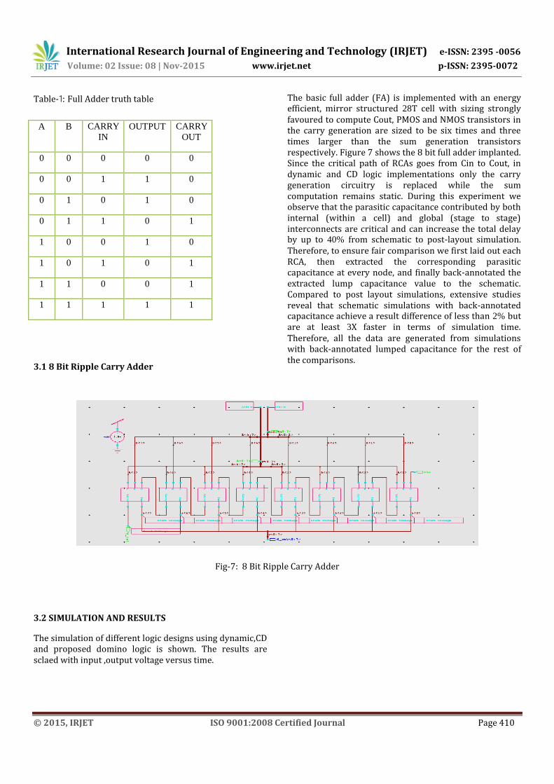
3.1 8 Bit Ripple Carry Adder
The basic full adder (FA) is implemented with an energy efficient, mirror structured 28T cell with sizing strongly favoured to compute Cout, PMOS and NMOS transistors in the carry generation are sized to be six times and three times larger than the sum generation transistors respectively. Figure 7 shows the 8 bit full adder implanted. Since the critical path of RCAs goes from Cin to Cout, in dynamic and CD logic implementations only the carry generation circuitry is replaced while the sum computation remains static. During this experiment we observe that the parasitic capacitance contributed by both internal (within a cell) and global (stage to stage) interconnects are critical and can increase the total delay by up to 40% from schematic to post-layout simulation. Therefore, to ensure fair comparison we first laid out each RCA, then extracted the corresponding parasitic capacitance at every node, and finally back-annotated the extracted lump capacitance value to the schematic. Compared to post layout simulations, extensive studies reveal that schematic simulations with back-annotated capacitance achieve a result difference of less than 2% but are at least 3X faster in terms of simulation time. Therefore, all the data are generated from simulations with back-annotated lumped capacitance for the rest of the comparisons.
Fig-7: 8 Bit Ripple Carry Adder
3.2 SIMULATION AND RESULTS
The simulation of different logic designs using dynamic,CD and proposed domino logic is shown. The results are sclaed with input ,output voltage versus time.
A B CARRY
IN OUTPUT CARRY
OUT
0 0 0 0 0
0 0 1 1 0
0 1 0 1 0
0 1 1 0 1
1 0 0 1 0
1 0 1 0 1
1 1 0 0 1
1 1 1 1 1
International Research Journal of Engineering and Technology (IRJET) e-ISSN: 2395 -0056
Volume: 02 Issue: 08 | Nov-2015 www.irjet.net p-ISSN: 2395-0072
© 2015, IRJET ISO 9001:2008 Certified Journal Page 411
Fig-8: Simulation Result Using Dynamic Domino Logic
Fig-9: Simulation Result Using CD Logic
Fig-10: Simulation Result Using Proposed Logic
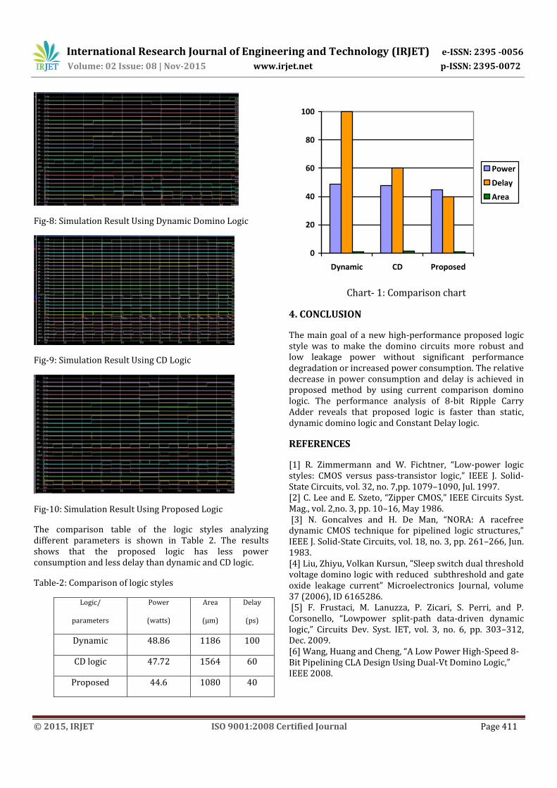
The comparison table of the logic styles analyzing different parameters is shown in Table 2. The results shows that the proposed logic has less power consumption and less delay than dynamic and CD logic.
Table-2: Comparison of logic styles
Logic/
parameters
Power
(watts)
Area
(µm)
Delay
(ps)
Dynamic 48.86 1186 100
CD logic 47.72 1564 60
Proposed 44.6 1080 40
0
20
40
60
80
100
Dynamic CD Proposed
Power
Delay
Area
Chart- 1: Comparison chart
4. CONCLUSION
The main goal of a new high-performance proposed logic style was to make the domino circuits more robust and low leakage power without significant performance degradation or increased power consumption. The relative decrease in power consumption and delay is achieved in proposed method by using current comparison domino logic. The performance analysis of 8-bit Ripple Carry Adder reveals that proposed logic is faster than static, dynamic domino logic and Constant Delay logic.
REFERENCES
[1] R. Zimmermann and W. Fichtner, “Low-power logic styles: CMOS versus pass-transistor logic,” IEEE J. Solid-State Circuits, vol. 32, no. 7,pp. 1079–1090, Jul. 1997. [2] C. Lee and E. Szeto, “Zipper CMOS,” IEEE Circuits Syst. Mag., vol. 2,no. 3, pp. 10–16, May 1986. [3] N. Goncalves and H. De Man, “NORA: A racefree dynamic CMOS technique for pipelined logic structures,” IEEE J. Solid-State Circuits, vol. 18, no. 3, pp. 261–266, Jun. 1983. [4] Liu, Zhiyu, Volkan Kursun, ”Sleep switch dual threshold voltage domino logic with reduced subthreshold and gate oxide leakage current” Microelectronics Journal, volume 37 (2006), ID 6165286. [5] F. Frustaci, M. Lanuzza, P. Zicari, S. Perri, and P. Corsonello, “Lowpower split-path data-driven dynamic logic,” Circuits Dev. Syst. IET, vol. 3, no. 6, pp. 303–312, Dec. 2009. [6] Wang, Huang and Cheng, “A Low Power High-Speed 8-Bit Pipelining CLA Design Using Dual-Vt Domino Logic,” IEEE 2008.