rf vacuum 1< microelectronics · iti ! a iyii si rf vacuum 1< microelectronics final report...
TRANSCRIPT

! ItI IyII a si
RF VacuumMicroelectronics1<FINAL REPORTContract No. MDA972-91-C-00328 August 1993RAY/RD/S-4921
Prepared forAdvanced Research Project AgencyDefense Sciences Office
I Prepared byRaytheon CompanyResearch Division131 Spring StreetLexington, Massachusetts 02173
IDTICAft ELECTE
U AUG18 199 3
I
~~~proe oublic 10I100W
13 893-1914593 17 0 4

Form ApprovedREPORT DOCUMENTATION PAGE OMB No. 0704-0188
Public tepoitmg butde for v* amo olooi 0 inom~ation is estiataed to average ¶ hour PW 1118POrse. W1C011ding" time for111 icr rvlieg Ilnjctruci. reseer01,ng e"Istng data sources. gattortig andmaiutatning e Janeeded end ccmpihe*g and reviw4ng the collection of inlonaltion. Send Comniflt regarding this burden estimate or any other -ipeol Ol dua collection 01 inolalon.inlidg iggeI" for rediucmg tis burden. to Washington Headquarters Services, Direcloral for Information Operations aN ROrPa. 1215 Jeffelron D•vis Hlighway, Sue1204. Arlinton, VA22202-43. and to ft Office at Management and Budget, Paperwork Reduction PmjeWt (0704-0188). Washinglon. DC 20503.
1. AGENCY USE ONLY amw B/ank) 2. REPORT DATE 3. REPORT TYPE AND DATES COVERED
August 9, 1993 Final - 1 October 1991 to 31 March 19934. TITLE AND SUBTITLE 5. FUNDING NUMBERS
RF Vacuum Microelectronics Final Report CMDA972-91-C-0032
S. AUTHOR(S)
Dr. Alan Palevsky
7. PERFORMINGORGANIZATION NAME(S) AND ADDRESS(ES) 8. PERFORMING ORGANIZATIONRaytheon Company REPORT /SNUMBER.
Research Division131 Spring StreetLexington, MA 02173
9 SPONSORING I MONITORING AGENCY NAME(S) AND ADDRESS(ES) 10. SPONSORING&MONITORING
ARPA AGENCY REPORT NUMBER
3701 North Fairfax Drive F33615-87-C-1507Arlington, VA 22203-17 14
I11. SUPPLEMENTARY NOTES
12a. DISTRIBUTION I AVAILABILITY STATEMENT 12b. DISTRIBUTION CODE
Approved for Public ReleaseDistribution Unlimited
13. ABSTRACT (MArnum 200 Words)
The result of the 18 month research and development project on high frequency Field Emission Array(FEA) cathodes is presented. Details of the process development and test procedures are discussed. Theresults relative to the program goals are presented. Finally, suggestions for future work in the 12 monthoption portion of the project are presented.
14. SUBJECT TERMS 15. NUMBERS OF PAGES
30Field Emission, Vacuum Tubes, Cathodes 16. PRICE CODE
?17. SECURITY CLASSIFICATION tI. SECURITY CLASSIFICATION 1. SECuRrrcTYLAssIFIcAnON 20. UMITATION OF ABSTRACTOF REPORT OF THIS PAGE OF ABSTRACT
Unclassified Unclassified Unclassified3,N,,40.Ot-2W5.6W0 STANDARD FORM 296 (Rev. 2.49)

RAYTHEON COMPANYResearch Division131 Spring Street Accesion For
Lexington, MA 02173 AsFNTIS CRA&IDTIC TABUnannounced ElJustification
RF VACUUM MICROELECTRONICS By ..........Distribution I
Availability Codes
Avail and I or
Dist Special
W DTIC QUALrY rNSPEcrP 3
I RAY/RD/S-4921 8 August 1993
I
I Contract No. MDA972-91-C-0032
I5 Sponsored by
Advanced Research Project AgencyDefense Sciences Office
IIIU

m S-4912
TABLE OF CONTENTS
Section Page3 1.0 INTRODUCTION .......................................... 1-1
2.0 PROCESS DEVELOPMENT .................................. 2-1
2.1 Overview ................... ......................... 2-1
2.2 Tip Emitter ...................................... 2-1
U 2.3 Circular Edge Emitter ............................ 2-7
2.4 Specialized Process Equipment .................... 2-7
3.0 TEST TRIODES .......................................... 3-1
3.1 overview ......................................... 3-1
3.2 Planar Triode (MMIC) Approach .................... 3-2
3.2.1 Test Stand and Chip Layout ................ 3-2
3.2.2 DC Results ................................ 3-8
3 3.3 Cylindrical Triode (Tube) Approach ............... 3-17
4.0 CAPACITANCE MEASUREMENTS .............................. 4-1
3 5.0 CONCLUSIONS .......................................... 5-1
IIUIIIUm iii
I

S-4912
LIST OF ILLUSTRATIONSUFigure No. Page
2-1 A Portion of a Fabricated Tip Emitter ArrayCathode .......................................... 2-2
2-2 Schematic of Process Steps for Bi-Level Tip3 Emitter ....... ......................... . ........ 2-3
2-3 (Top) Tip Above Gate and (Bottom) Tip Below Gate.2-6
2-4 Single Circular Edge Emitter ..................... 2-8
2-5 Array of Circular Edge Emitters .................. 2-9
1 2-6 Circular Edge Emitter in Cross Section ........... 2-10
2-7 Custom Evaporator with Load Lock and PrepChamber .......................................... 2-12
3-1 Custom UHV Compatible FEA Test Stand ............. 3-3
m 3-2 Computer Controlled Bakeout of Test Chamber ...... 3-5
3-3 Layout of First Iteration of Planar TriodeCathode Chip ...................................... 3-6
3-4 DC Test Alumina for Cylindrical and Planar3 Triode Cathodes .................................. 3-7
3-5 Composite Fowler-Nordheim Plot of TypicalData - Total Current ............................. 3-9
3-6 Composite Plot - Current per Tip ................. 3-10
3-7 Composite Plot - Transconductance per Tip ........ 3-11
3-8 IV Plot of Highest Current Device ................ 3-12
3 3-9 Low Current Transfer Characteristics ............. 3-14
3-10 High Frequency, Bakeable, UHV Flange ............. 3-15
3 3-11 Layout of High Frequency Alumina .................. 3-16
3-12 Equivalent Circuit for Planar Triode............. 3-18
1 3-13 S11 Input Match for Planar Triode................3-19
3-14 $21 Transmission for Planar Triode ............... 3-20
3-15 $12 Isolation for Planar Triode................3-21
1 3-16 $22 Output Match for Planar Triode.............. 3-22
l iv
1

m S-4912
r NLIST OF ILLUSTRATIONS (Continued)
Figure No. Page
3 3-17 Layout of Cathode for Cylindrical Triode ......... 3-23
3-18 Equivalent Circuit for Cylindrical Triode ........ 3-253-19 Measured and Extrapolated Ft for Cylindrical
Triode ................. ............. .......... 3-26
4-1 Layout of Second Iteration of Planar TriodeCathode Chip ............. ..... ................ 4-2
4-2 Enlargement of 20 Edges Structure ................ 4-3
4-3 Enlargement of 25 Under Dense Structure .......... 4-4
4-4 Enlargement of Dense Square Structure ............ 4-5
4-5 Design Parameters of Planar Triode Cathodes ...... 4-6
4-6 Best Fit of Measured Data to CapacitanceModel - Silicon .................................. 4-8
4-7 Best Fit of Measured Data to CapacitanceModel - Sapphire ................................. 4-8
v

m S-4912
1.0 INTRODUCTION
Vacuum Microelectronics technology is an attempt to combine
3 the best features of low cost solid state fabrication techniquesand vacuum tube electronics. One goal is the development of
m cathodes that can be modulated at the carrier (not a modulation)
frequency. This concept has worked well at UHF frequencies withgridded cathodes to reduce tube size and increase efficiency. To
push this concept up into the microwave frequencies requires a new
technology. This is because the small grid spacings required cannot be manufactured with conventional tube technology. The newtechnology is micron-sized gated field emission cathode arrays.3 The program goals were to fabricate triode structures that met thefollowing criteria:
1. Ft = gm/2tCg > 1 GHz2. vg < 250 volts
. J >5A/cm2
4. I >5mA
The nomenclature for the triode's ports is a mixture of solidstate FET and tube terms. The electrons start from the field
emitter cathode (source), are modulated by the gate (grid), and arecollected by the anode (drain).
The first criteria Ft is the ratio of the small signal3 transconductance to the gate capacitance C 9* This a measure of
the maximum operating frequency of the triode. The second criteriaV V is the gate voltage required to obtain the gm in the first term
and J and I in the following terms. J is the current density and Iis the total current at the operating point. The operating life
3 had to be at least one hour. The anode voltage and duty cycle werenot specified.I
Im 1-1
U

I S-4912
Section 2.0 presents the processes developed to fabricate the
cathodes. Two types of cathodes; tip and circular edge are
described. Section 3.0 presents the results from two test
approaches; a planar (MMIC like) triode and a cylindrical (tube
like) triode. Section 4.0 is a detailed investigation into the
3 gate capacitance issue. Section 5.0 concludes with suggestions for
future work.
I1IIIIIIIUIIII3 1-2
I

I S-4912
2.0 PROCESS DEVELOPMENT
2.1 Overview
Two emitter structures were fabricated; tip and circularedge. The process development was started for another application
under Raytheon Company IR&D funding. The processes were extended
and improved under this contract. Standard semiconductor
processing is used where possible. Stepper photolithography wasused for all the masking steps. The two processing steps that3 required extensive work over conventional techniques were in theReactive Ion Etching (RIE) of the metals and the thick metal
3 evaporation steps.
All the emitter devices use molybdenum for all metal layers.
Molybdenum may not be the best choice because there are materialswith smoother surfaces and/or lower work functions that may give3 higher emission currents for a given gate voltage. Also, there aresome processing difficulties with molybdenum, such as its3 relatively poor adherence to the silicon dioxide dielectric layers.However, the silicon dioxide to molybdenum etch rate ratio is veryhigh which makes for a relatively easy stack etch.
2.2 Tip EmitterIOur baseline approach is to form a conventional micron
sized tip Field Emission Array (FEA) cathodes using a metal
insulator stack on a metal layer on which cone-type field emittersare formed. The metal layers are 3,000 angstroms of molybdenum andthe dielectric layers are 8,000 to 10,000 angstroms of lowtemperature CVD oxide (LTO). The tips are made by evaporation into
Smicron sized holes spaced on 6 micron to as small as 2.5 microncenters (see Figure 2-1). The process is illustrated in Figure
3 2-2, Steps I through X.
1 2-1
I

3 S-4912
3 PBN-92-372
U2U
Fiue21N oto faFbictdTpEitrAryCtoe2-
I:PVU L ODI 03NTPP UL EI=FFOU O

3 S-4912
L Substrite Preparation 7Ther5Jly Grown PBN-93-1 880
-Sl~Own DNaode
Subutrate3 N. First Metal Deposition and PatterningREA zo4- MoIybdenw,
Ill. Dielectric Deposition
4-CVD Samn Nodde
3 IV. Second Metal Deposition and Patterning4 Mo~bftnixfl
3 V. Stack Etch
3 - SiliconSilicon Dioxide
VI. Parting Layers Molyb~denumn3 Partng 1PartingLayers Layers*
IX. Tip Formation: Excess Metal Removal
3 VII. Tip Formation: Metal Deposition 50%~/o~ -4 4- Molbden
SPartingPatnLayers Layers11191 NEEE
3Vill. Tip Formation: Metal Deposition 100%
4-Molybdenum .TpFrainrEcs eaneoaParting X i omto:Ecs ea eoa
Figure 2-2. Schematic of Process Steps for Bi-Level Tip Emitter.
3 2-3

S-4912
For a silicon substrate a blanket SiO2 layer is grown for
I insulation (Figure 2-2, Step I). For a sapphire substrate, this
step is not required. Next, a molybdenum layer (Ml) is deposited
by sputtering and then patterned (Step II). A blanket Si02dielectric layer (D1) is then deposited by Chemical VaporDeposition (CVD) (Step III). The top moly layer (M2) is then
deposited and patterned to form the gate electrode (Step IV). Thetop metal is then masked to define the cavities and then the stack
is then is vrti.cally etched by a reactive ion etch (Step V) to
form cavities abcut 1 pm in diameter. Next, the surface is coated3 and the upper sidewall (not the lower sidewall of the cavities) by
a low angle evaporation with a set of stress relief and release
layers (Step VI). To form the tips, approximately 1.5 pm of
molybdenum is evaporated onto the substrate. The molybdenum forms
a cone in the cavity due to a gradual closure of the cavity opening
(Steps VII and VIII). As the tip material is evaporated, it coatsthe top of the release material and the sides of the metal aperture
Sdefining the cavities at the emitter sites. Since the aperturesidewalls are continually coated as the tips are formed, theopening at the top of the cavity becomes gradually smaller
resulting in the conical shape of the tip. After tip formation,the excess molybdenum is selectively removed by dissolving the
release layer (Steps IX and X). More details of some of steps arediscussed below.I
The MI and M2 metalizations are patterned for interconnect.At crossovers, there is a step. It was found that the M2 layer was
cracking at this edge. The Dl depositions step was modified to
solve this problem. First 1,000 angstroms of LTO (low temperature
oxide) is deposited. This is followed by 8,000 angstroms ofphosphorous oxide doped LTO. The dielectric is then re-flowed to3 smooth out the steps. This is followed by a final 1,000 angstromsof LTO. The addition of these process steps eliminated the
3 crossover cracking problem.
21 2_4
I

I S-4912
Reactive ion etching is required to etch the cavity in Step V.
For the standard tip emitter, two layers must be etched; they areone 3,000 angstroms layer of molybdenum and one 8,000 to 10,000
angstroms silicon oxide layer. A multistep etch, based onalternate chlorine and fluorine chemistries for molybdenum andsilicon oxide etching, was devised. There are no constraints
placed on the molybdenum-to-oxide etch rate ratio since there is no
strict requirement that the molybdenum etch stop on oxide.
However, the oxide etch requires good selectivity to molybdenum sothat the bottom layer of molybdenum is not etched into after the
last oxide layer is etched away and that the top moly layer is notetched after the photoresist has been eroded away.
The height of the tip made in Steps VII and VIII is determinedby the diameter of the hole. If the hole is too small, the tip
will be below the gate and if the hole is too large, the tip willbe above the gate. The lithography of the hole diameter iscontrolled to within plus/minus 0.1 micron. Even if the holediameter is controlled, variations in the dielectric thickness will
effect the placement of the tip relative to the gate. Figure 2-3
shows these two cases.
Due to the thick layer of molybdenum necessary for the tipformation (Steps VII and VIII), peeling and cracking due to the
induced stress was found in M2 after the excess molybdenum wasremoved. This problem was resolved by modifying the release layerto include an additional layer that stopped the stresses from
propagating down to the M2 layer.
Initially, there were many shorts between the twometalizations on the first wafer lots. It was found that theshorts were there even if the tips were not deposited. The culpritwas the residues left from the RIE of the holes (Step V). An
improved hot solvent clean solved the problem.
* 2-5

I S-4912
I PBN-91-0644
I2--coy&AALIODI OSNTpM ~rLGBEEPOUTO

S-4912
2.3 Circular Edge Emitter
There was a second process development effort tofabricate fine circular edge emitters. First, using an oxidizedsilicon or sapphire wafer the same metal-oxide-metal layers used inthe tip process are made. The appropriate gate and emitter
electrodes are patterned in this step. Then a 5,000 angstromsoxide inverted mandrel layer is deposited and a 2,000 angstroms3 titanium layer is deposited. Next, micron-sized holes arepatterned where the emitters are desired. The titanium and oxidelayers are reactive ion etched and the resist stripped. The
titanium is now the mask for further etching and the cylindrical
opening is the inverted mandrel for the circular edge. Half of the
top moly layer is back-sputtered onto the oxide mandrel and theremainder is etched by RIE. Finally, the oxide mandrel is etchedaway. Figure 2-4 is a SEM of one of these structures from anoblique angle and Figure 2-5 shows an array on six micron centers.Figure 2-6 shows a structure in cross section. The fine edge is onthe order of 100 angstroms wide and quite uniform.
I In reverse to that of the tip field emitters, the gate is thebottom electrode and the emitter is the top. Gate voltage will3 generate an electric field that will spread through the centralhole and in theory create field emission from the edge. In3 practice, no emission currents were found. This work was then"discontinued and all our process development efforts were on the
tip type of emitters.
2.4 Specialized Process Equipment
A major capital investment was made in a customevaporator for this program. The unit features two 30 cc four-pocket electron beam hearths for individual or co-evaporation; sixhead quartz crystal and electron impact spectroscopy disposition
monitoring; three-inch MBE manipulator with programmable substraterotation and azimuthal control; gridless low energy ion source for
2-7

'U S-4912
PBN-92-207
Ii
Fiue24IigeCrua deEitr
2-COYIAAL ODI OSNTPRM UL EIIEPPOUTO'

S-4912
PBN-92-206
Figure 2-5. Array of Circular Edge Emitters.
2-9
C)OPY AVApALE To DTIC DOES NOT PERJiT FULLY LEGIBLE REPRODUCTON

S-4912
PBI2-0
Fiue26IiclrEg mte nCosScin
2I1COYIAIB O= OSNTPEMTF YLGL ERD1M?

I S-4912
substrate pre-clean or reactive co-deposition; RF sputter source;load lock and prep chamber with substrate bakeout up to 4500 C; and
a 36-inch throw. The unit is fully operational and is used for allthe evaporation steps in PEA cathode fabrication. The unit is
shown in Figure 2-7.
IIII
II
IIIIUIII 2-11
I

S-4912
Ic-908#
4t
I8
IA
Figure 2-7. Custom Evaporator with Load Lock and Prep Chamber.
2-12

m S-4912
3.0 TEST TRIODES
3.1 OverviewIThe electron emission from field emission cathodes is3 modeled with the Fowler-Nordheim Equation given below.
I = av 2 exp (-b/V) (amps)
where
a = aAJ2 exp BLr144 x10]ITI I t1/2
b = 0.95Bt3/ 2 /13
IA = 1.54 x 10⁻⁶
a = emitting area
B = 6.87 x 10⁻⁷
S= field enhancement factor at surface
N = surface work function
I By taking the derivative with respect to V, gm may be obtained
gm= I b) (Siemens)
IThe two parameters a and b fully specify the functional form.The term a scales as field enhancement due to curvature and the
I closeness of the gate electrode. This term is on the order of 1.5x 10⁻⁶ amps/volts 2 per tip and needs to increase for improvedperformance. The term b scales, as the surface work function, is
on the order of 1000 volts and should decrease for improvedperformance. The conventional way to plot data is I versus 1000/V.Fowler Nordheim I/V performance will appear as a straight line withthis scale for the typical field emission parameters encountered in
S this study. Also on this type of plot, the farther the curve is to
13-1

S-4912
the right (larger 1000/V, decrease in b term) and the more vertical
(increased I for a given V, increase in a term), the better thedevice.
As opposed to solid state devices, the "processing" of FEAs is
not complete after the chip comes of the fabrication line. Afterthe wafers are diced into chips, they are H2 (atmospheric pressure)
fired at 400 degrees centigrade for 20 minutes. The chips are kept
in a dry N2 atmosphere whenever possible. The bonding and final
assembly are done in air. The initial turn-on is not instantaneous.
The voltage is gradually increased over at least 24 hours before
getting full current. This turn on may be though of as a
continuation and the final step of the "processing".
Two test vehicle approaches were used to evaluate high
frequency FEA performance. The first approach is a planar cathodein a test chamber. The second is a cylindrical micro-triode tube.
3.2 Planar Triode (MMIC) Approach
3.2.1 Test Stand and Chip Layout
m To test these arrays electrically, it is necessaryto bake and test them in ultra-high vacuum. A test station for
3 this purpose has been fabricated under company funds. The deviceunder test is bonded to a ceramic circuit board, which contains3 metal leads which are wire-bonded to the FEA and, through a vacuumfeedthrough, connect to electrical power supplies and RF measuring
equipment. The vacuum system is bakable to 450 0 C. We also are
able to test more than one chip at a time. The test stand is shownin Figure 3-1.U
The pumping system consists of a sorption pump, followed by a3 turbo pump and then a vac-ion pump. There is no mechanical oil
fore-pump in the system. The system is capable of vacuum on the
S10-10 Torr. There is a residual gas analyzer and a microscope for
* 3-2
I

U S-4912
IW1-1RW" C-93
...... ..Iý9
I li r
Ij
3 Figure 3-1. Custom UHV Compatible YEA Test Stand.
I 3-3

I S-4912
direct viewing through a window. The power supplies allow
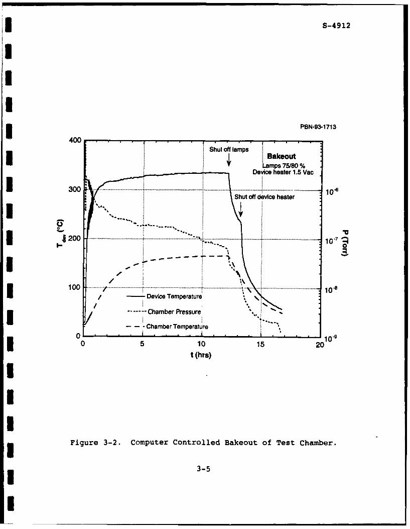
operation up to 10 KV although most tests were performed under2 KV. There is also a moderate voltage (250 volts) gate pulser3 that allows for low duty operation. Most of the equipment is ableto be controlled by a computer. The bakeout sequence, the initialdevice turn on, and the measurement of I/V characteristics areunder program control. Figure 3-2 shows a typical bakeout run.The layout of the first iteration planar chip is shown in Figure
3-3.
3 The chip size is 3 mm square. It has seven bondable devicesplus an additional five RF probeable structures. The top device is3 a two-port structure to allow for "tuning". The balance of thedevices are one port. The bonding pads along the sides are in aground-signal-ground configuration with a shared ground. They are
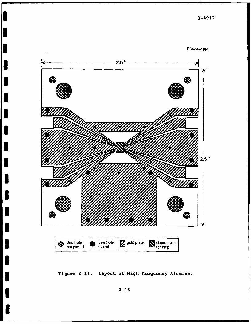
gold plated to allow for bonding to the alumina. The pitch ofthese pads is 300 microns. Closer into the devices are RF pads on3 a 100 micron pitch. The dc/low frequency alumina is shown inFigure 3-4.
The alumina is 2.5-inches square. The planar triode chips fitinto the lower (larger) depression. This allows the wire bondingto be flush and eliminates the high voltage at the chip edge. Thealumina is mounted on a test flange that itself mounts on the test3 chamber. Wires are bolted to the alumina and then lead to thevacuum feed-thru's on the flange. A heater is placed on the
I backside of the alumina. The anodes were made from a variety ofmaterials including stainless, copper, and molybdenum. The firedmoly anodes appeared to give the results. For the high current
tests, we were worried that the anode might be the limiting elementfor proper operation; therefore, high current tests were performed3 at low duty cycle. The cathode anode spacing was typically 1 tofive mm. For all the tests of the planar triode, the device was3 configured in a common emitter configuration with the emittergrounded, the anode at a positive high voltage and the gate driven
i positive to turn the device on.
* 3-4
I
S-4912
40 PBN-93-1713
400 ..
Shut off lamps3BakeoutLamps 75/80 %
Device heater 1.5 Vac1 -00- .. . ;-.-;;r........ ,
3 0 0 .. ............................... ...... ................................ ...... ."- :- ....... ............ ....... ................. .............. ....... .................Shut off device heater
2 0 ............ ......................... .. .................... ------,-. ------" .... ....... .......... -- 1 0 -7 0-
...... . .......\................ ..... .......... .. .... ! ............... ............... ........... l -
1j 00 ....... -/. . . . . .............
/Device Temperature 0
I /...Chamber Pressure -
- - - Chamber Temperature
0 10-90 5 10 15 20
t (hrs)III
SFigure 3-2. Computer Controlled Bakeout of Test Chamber.
i 3-5
I

S-4912
' 3 ~PBN-93- 860
6,541 TipsOpn289rs_r8 pF .. 2p
3 .5 gm pitch 2L__
,i
I 6,541 Tips
2,4 Tis8 pF 2,916 "ips
D ý )3gm Pitch 9 nro
D8 pF nn8 pF
K 0
S03000 gm
Figure 3-3. Layout of First Iteration of Planar Triode Cathode
Chip.I3-6
I

U S-4912
PSN-93-1865
SMI M12
STII2SRPM
COMMON MI (STRIP M2) COMMON M I ISTRIP M2)I2
thru ole hru ole god plate *depression
Figure 3-4. DC Test Alumina for Cylindrical and Planar TriodeI Cathodes.
I 3-7

S-4912
3.2.2 DC Results
A composite Fowler-Nordheim plot of typical
performance data is shown in Figure 3-5.
The M and o data are from chips that used mask developed under
company IR&D funds. As can be seen by a variety of the curves, thetotal current goal of 5 milliamps at a gate voltage less than 250volts was met. The emitting area for the a and o data (from thecontract mask) is 0.05 cm squared. The total current required to
meet the current density goal of 5 amps/cm2 is 12.5 ma. Both thesecurves exceed that value. The data is also presented normalized tothe number of tips in Figure 3-6.
The best performance obtained was 14 micro-amps per tip. Fromthe spread in the data and from other single tip measurements, thecurrent is not equally spread out over the tips. Because of the
exponential form of the emission and the lack of any currentlimiting resistors (ballast), we suspect that only a percentage of3 the tips are carrying the current. Therefore, the actual peak tipcurrent load could be much higher.
m The dc gm normalized per tip data is shown in Figure 3-7.
m The 2 micro-Siemens per tip value is close to what is requiredto meet the Ft goal of 1 GHz. The goal was not met.
The best current performance seen in the planar configurationis shown in Figure 3-8.
This was a 5000 tips array that gave 14 micro-amp per tip and
0.8 micro-siemens per tip. This device was operated at 2% duty andwas on a sapphire substrate.
1 3-8

I S-4912
I
IU PBN-93-1817
Composite IV
-- 2916 tips................ I ..... .... . . . . ................. ... .. 4 5 0 0 tips -..--
I 101 - 1. . .. 45000 tips ...
-- 5000 tips1 0 . . . . . ... ............... ........... . ...... ... ... .... ....... .. . -.... 2 91.tip s.....
100 -- 2916 tips
--o---1600 tips
II
1 102....I~~~~...... .... ......... ... . . . .......
i o- .....
I~V <250
3 5 7 9 11 13 15 17 19I 1000N
IFigure 3-5. Composite Fowler-Nordheim Plot of Typical Data - Total
Current.
I 3-9
I

S-4912
III
Composite IV PBN-93-1818
102. ....................... C ' :
-2916 tips
......... ..... .................................................................. .......................... ............. 4., 000,,,, s10 ...................... ...... ..................... .i ....... .iiii .................. ....... ......................1 45000 tips
.•0 " .... .... .... ....................................... ..... ....... ':... ....... ...... ........................ .. .............. .............
I ..... 000.tip32160 tips
2160 tips
Ii _
Su2 .. .-...... .......................... . 26 tip.
I.
. ...... ...... ......... .......
10 65 1 . . . . . . . . Ii0 . . .. . . . . . 1 5 . . . . . . . . . 201000N
Figure 3-6. Composite Plot - Current per Tip.
g 3-10

m S-4912
IIII
n Composite g /tip PBN-93-1714
3101 . .
_ 2 LS /tip! gn/tip( OS)
100....... . ... - .. ....... ..-
,o.* .......... ....... .. ..... -..
S • 1 0 -3 .. . . . . .... ........... ......... .............. ............ .... . ... .. .... ......................
10-O 4 . . . ... . .... ................. .......................... ......... .. ............. ........ .. ............. .... ...... ......... ..... .....1.. .......
10O .. .. .... , ........ ....................... ....................... .................... ....... ............... ....... .................... . .... ........... ...
I ,
10.
4 6 810 12 14 16 1820
I
i Figure 3-7. Composite Plot - Transconductance per Tip.
I 3-11
I

S-4912PBN-93-1 7121 80 r 2T22&-1.8.pl 0
370.... ............... .......
60 -----
40 ...... ..
1 20
60 80 100 120 140 160 180V
2T22a-1 .8.plO100 . . .. . 10I- -I =1.0X1 0 2 V2
e*1131
-- g g(2+1213N) IN
0\1
1.10 ............ ...... 0 0
0.0 0 .0
6 7 8 9 10 11 12 13
Figure 3-8. IV Plot of Highest Current Device.
3 3-12

I S-4912
The data presented above was all at anode voltages between 500
and 1000 volts. The transfer characteristics of a typical deviceis shown in Figure 3-9.I
This data looks more like conventional tube pentode data as3 opposed to triode data. This can be explained by the fact that thegate to emitter spacing is much smaller than the gate to anodespacing. Therefore, the anode voltage does not effect the anode
current except when it is near or less than the gate voltage. Atthese low currents, there are no space charge effect. At thecurrent levels anticipated to meet the Ft requirements, space
charge will be a consideration.
I 3.2.3 RF Results
I The test flange and alumina used for the dc/lowfrequency testing does not work above frequencies of 10 MHz. A
fkhigh frequency flange and alumina were fabricated that work up to10 GHz. The high frequency flange is both bakable to 450 0 C and UHVcompatible. It features four RF leads for the cathode, one anodelead, and a variety of dc leads for bias, heaters, etc. The unitwithout the alumina in place is shown in Figure 3-10. The high
frequency alumina layout is shown in Figure 3-11.
The four coaxial cathode leads are clamped to the co-planarlines that are tapered down to the chip maintaining a constant
I 50 ohm impedance. The anode cantilevers over the cathode from thebottom. The additional ground beneath the anode was added for
improved RF match. The chip has four leads per side while the
alumina has only two. This is because of space limitations.Therefore, the chip may be slid up or down in the depression to
I choose the first and third or second and fourth row.
I Modulations of a simple triode at low level have been observedwith our first iteration of planar triode chips. A square area of0.5 -m square with 26,244 tips was run at 150 micro-amps at 72.3
gate voltage and 500 volts on the anode. This was performed CW so
I 3-13
l

I S-4912
I
PBN-93-1715
Device 2T24A-3.3.53
----------- V m,72.4
IIS, ,V -68.7
100 • -- V -65.T ..
SV -62.0
-- IF"-'--"V -59.9
310"1 •-J.--V *57.7....
I
I v-54.5
V -V2.5
10-2 v I . .. I . -. . ..a.. n I n t ..
0 100 200 300 400 500AV
II3 Figure 3-9. Low Current Transfer Characteristics.
3 3-14
I

S-4 912
I )
I10
Il
Fiue31.HgIrqecy aebe H lne3I1
I S-4912
5 ~PBN-93-1694
3 2.5
3 2.5"
not plated plated
3 Figure 3-11. Layout of High Frequency Alumina.
3 3-16

IS-4912
the Vector Network Analyzer (VNA) could measure the S-parameters (apulsed VNA is not available in our lab). The equivalent circuitfor the tests are shown in Figure 3-12.
The source and load are in the VNA. The bias-T circuitscombine the RF signal with the dc bias voltage while isolating thesource and load form the high voltages. The operating bandwidth ofthe bias-T is 30 MHz to 3 GHz. The results were not de-embedded to
the device plane and therefore include the parasitics of the
alumina and the flange. The gate capacitance includes 8 pF from
the chip and 2 pF from the alumina. The anode and isolationcapacitance is due to the parasitics of the unshielded anode
geometry. There is also an input resonance due to the cavity ofthe chamber that is not included in this equivalent circuit.
m The four S-parameters of the device are shown in the off andon state in Figures 3-13 to 3-16.
Since the device is highly mismatched on the input and outputin a 50 ohm system and is relatively low gain, only a differentialchange in insertion loss is seen on the S21 curve (Figure 3-14).
The fact that $21 shows a change while S12 does not change when thedevice is turned on indicates a true gain mechanism and not just avariable attenuator. Because of the resonance, feedthrough due tothe isolation capacitance is not seen clearly above 0.30 GHz.Since on the $21 data, the hot curve is above the cold curve up to1 GHz indicates that modulation is occurring (albeit weakly) up tothat frequency.
I 3.3 Cylindrical Triode (Tube) Approach
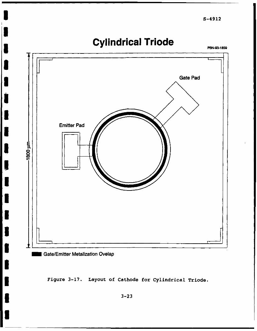
The cathode for the micro-triode is a 700 micron annuluswith seven concentric circles of 714 tips per circle for a total of
4,998 tips and a calculated parallel plate capacitance of 1.55 pf.The layout of the cathode is shown in Figure 3-17.
I* 3-17
I

II S-4912
I
I
PBN-93-1711
5 Equivalent Circuit For Planar Triode Tests
[Iso RAI
IKII LII -- C LBT I
I I_ I --- -- - •
L -d Vg L - - - I IdcVa L/3 Source Bias T FED Bias T Load
- 50 ohm Coax
IR - R, = 50 a Cg = 10 pF fin - 320 MHz Rg = 6.5 0CBT= 1000OpF CA=O0.8 pF fout-=4.0OGHzRA=60f
I LBT =820OI±H Ciso =.050pF gm= 30pS
II
Figure 3-12. Equivalent Circuit for Planar Triode.
5 3-18
U

5-4912
VME2 3gm 162 x 162 2T24A-3430 1 tt ,, L I I I i I I I I I I I I I
0
-2
I1
-- Cold
--- Hot
-4
I -- ______ ____ ___
-5I I I I I I I I I I
0.00 0.20 0.40 0.60 0.80 1.00
Frequency (GHz)
I Figure 3-13. S11 Input Match for Planar Triode.
3-19

S-4912
PBN-93-1707
VME2 3gm 162 x 162 2T24A-34-20
-30
C I
I (A -40 Cold
- ............. Hot
-50 _ -I50 ___Ii~ (_
-60 [ I I I I0.00 0.20 0.40 0.60 0.80 1.00
Frequency (GHz)
I
Figure 3-14. S2 1 Transmission for Planar Triode.
3-20
I

S-4912
I
PM-93-1706
VME2 3 gm 162 x 162 2T24A-3.4
-2 0 II I 1 I I 1
3 -0
O)-50 - Cold
S- -- - Hot_
-600.00 0.20 0.40 0.60 -. 40 1.00
Frequency (GHz)
IFigure 3-15. S$.2 Isolation for Planar Triode.
S3-21
I~63 ______ __I _ I_

S-4912
I
I
VME2 31gm 162 x 162 2T24A-34-0.000 VII
, ____
S-0.600
S------- Cold-.800U0HotII!
-1.200
I -1.400' 1 11111 f II IiI I I I j
0.00 0.20 0.40 0.60 0.80 1.00
Frequency (GHz)
I Figure 3-16. S22 Output Match for Planar Triode.
3 3-22
I
S-4912
iCylindrical Triode P,9,15
Gate Pad
Emitter Pad
IrI -I
I
SGate/Emitter Metalization Ovelap
II Figure 3-17. Layout of Cathode for Cylindrical Triode.
1 3-23
I
S-4912
These chips were first tested in the chamber using the upper
position in dc test alumina (Figure 3-4). Good chips were selected
and sealed into a glass micro-triode. The equivalent circuit of
this device is shown in Figure 3-18.
This device was biased with the gate at dc ground and thecathode pulsed negative with a half sine wave rectified 60 Hz
signal (27% duty). The anode was held positive at 1,000 volts.
The measured and extrapolated data from this device is shown in
Figure 3-19.
The measured I/V data was fit to a Fowler-Nordheim curve to
calculate the gm (and therefore Ft) and allows extrapolation to
higher gate voltages. The measured data yields an Ft of 100 MHz.
Extrapolation to a gate voltage of 130 volts and a current of 60milliamps yields an Ft of 1 GHz. This is equal to 2 micro-siemens
per tip. Our best dc result (Figure 3-7) was 0.8 micro-siemens pertip. Therefore, this extrapolation is not too unreasonable. The
glass package of this device was limited in bandwidth to about
100 MHz and therefore microwave tests were not performed.
3-24

S-4912
MBN-93172
Equivalent Circuitfor Cylindrical Trial Tests
+VA
-10 kfl
RFOut
60 Hz 120 pF 620 pF
3.6 RF3.6 In 0_In
lOOmH 50 kQ
51kr T 120 pF
Figure 3-18. Equivalent Circuit for Cylindrical Triode.
3 3-25

U S-4912
U ~PBN-93-1 693
I FEA Micro Triode
4998 Tips, 3-micron Centers1 ~700 g~m Diameter Annulus800-
i=5mA C=1.4pf
60 gm=.88mS Ft=100MHZ
I~NI* ~400-
1 200-
I90 95 100 105 110 115 120 125 130
3Figure 3-19. measured and Extrapolated F t for Cylindrical Triode.
3 3-26

S-4912
4.0 CAPACITANCE MEASUREMENTS
It was realized after the first iteration was completed and5 tested that smaller devices were required to meet the Ftrequirement. Maximum capacitances of less than 0.2 pF are probably5 required. To this end, a second design, layout and fabricationiteration was performed on the planar triode design. The second3 iteration planar cathode layout is shown in Figure 4-1.
As before, variety of structures were included to helpcharacterize the capacitance. The top structure is a two-port thatallows the cathode to be "tuned". All the other structures are1 one-port. The second structure from the top is a series of 20edges each 120 microns long with 4 micron overlap of metalization
(Figure 4-2). The third structure is and under-dense array of 20
rectangles each 17 by 25 microns (Figure 4-3). The bottomstructure is a dense square 70 by 70 microns (Figure 4-4).
For each of the last three structures, there are four devicesSper chip. Two are connected to bonding pads, one is only RF
probeable and the last is also RF probeable but does not have any
tips. Also, along the bottom there is an RF probeable open, short,
and large capacitor. Wafers were fabricated on two differentsubstrates; sapphire and silicon, and with three different tip totip spacings; 4, 3, and 2.5 gun. A table of the design parametersand predicted characteristics are shown in Figure 4-5.
For each structure, the three different hole pitches arelisted. The value of Area-1 is the area of where there is
overlapped metal and is used to calculate the parallel platecapacitance. Given our target of 2 micro-siemens per tips, an Ftcan be calculated. The value of Area-2 is the total area forcurrent density purposes and is used to calculate J at out target
5 current of 20 micro-amp per tip.
4-1

S-4912
PMN-93-1861
VMERF Number 2-Planar Triode
Q,,
Ell
_x 170
250250 CAP
I
I3 25Cx25iJCAP
Uo~bl O[3 E 7D~-j
3000gm N
Figure 4-1. Layout of Second Iteration of Planar Triode CathodeChip.
* 4-2
I

i S-4912
I
IPBN-93-1862I
I I Emitter
U Gate
4 gmI
i Figure 4-2. Enlargement of 20 Edges Structure.
Ii Fiue424Elreet-f23desSrcue
U

S-4912
Emitter PBN-93-1863
I Gate
I 'lEmitter
20 gm
5 • Gate/Emitter Metalization Overlap
II
I Figure 4-3. Enlargement of 25 Under Dense Structure.
II 4-4
I

S-4912
I
I PBN-93-1864
I
1 Dense Square ConfigurationI
SEmitter
3 Gate 70Alm
31 Gate/Emitter Metalization Ovedap
UI
Figure 4-4. Enlargement of Dense Square Structure.
* 4-5
I

S-4912
I PBN-93-1799
Circuit Size(g~m) Pitch W/edge Number Area-1 C (pF) fT (GHz) Area.2 J(g~m) total (AtM2) pmalll @ 2 (cm2) (I/cm2)
IPlate j w Vts/tip @20
line 4xl720xl 4.0 429 429 6880 1.23 .593.0 572 72 6880 .23 .792.5 686 686 6880 .23 .95
20 edge 4x 120x20 4.0 29 580 9640 .32 .58 4.18e-4 2813.0 39 780 9640 .32 .78 4.18e-4 3712.5 47 940 9640 .32 .93 4.18e-4 45
425sr 210x 17x25 4.0 3 225 8500 .28 .26 2.25e-4 20
3.0 4 400 8500 .28 .45 2.25e-4 362.5 5 625 8500 .28 .71 2.25e-4 56
Dense 70x70xI 4.0 16 256 4900 .16 .51 4.9e-5 1043.0 21 441 4900 .16 .88 4.9e-5 1802.5 _2ý6 676 4900 1.16 1.3 4.9e-5 276
Figure 4-5. Design Parameters of Planar Triode Cathodes.
4-6
I

m S-4912
The structures were on chip RF probed with standard MMICprobes on a vector network analyzer. A TRL calibration was used onthe network analyzer and verified to 15 GHz. The phase delay of
3 S1 1 at 1 GHz was used to calculate the capacitance. The magnitudeis a measure of the loss. There was a constant 6 ohm loss that was3 independent of frequency that is assumed to be contact resistance.
At these frequencies it was not possible to see any loss due tometal resistance or dielectric. The total capacitance has been
approximated as:
Ctot = Ktips(KlayoutC11) + Cleads + Cpads
where C11 = o Aid is the calculated parallel plate capacitance,Cpads is from the bonding pads, Cleads is from the leads and RF
probeable pads, Klayout is for edge and other layout effects, andKtips is due to the hole and tip. The measurement of the largecapacitor is used to calculate 'd". The relative dielectric
constant for the SiO2 is assumed to be 3.7. The difference betweenthe devices with and without bonding pads is used to calculate
S Cpads* The dielectric thickness "d" was found to be I micron forthe silicon wafer and 0.8 micron for the sapphire wafer. A best
fit was made over many measurements and tabulated in Figures 4-6
and 4-7 for silicon and sapphire substrates respectively. The lasttwo columns indicate how good the fit is to formula.
These results show some surprising effects. First, is the3 difference in the parasitic and edge effects between the sapphireand silicon. It appears that the bottom SiO2 layer and the first
level metal do not completely shield the substrate and therefore
the substrate contributes to the stray capacitance. This effect isshown by the increased values of Klayout, Cpads, and Cleads of the
silicon relative to the sapphire. The second effect that isunexpected is the difference due to the tip density. For the3 silicon, the tips cause an increase in capacitance with increasingdensity while for the sapphire, there is a decrease. Anexamination of a silicon wafer with holes and no tips did not show
3 4-7
l

S-4912
PBN-93-1709a
Silicon substrate I d Im IpmDevice Tip Pitch CH Klayou Cdevce Ktps Cleads C ads Ctot C actType (tni) (pF) (pF) (pF) (pF) (pF) (pF)
caic. caic. caic. caic. meas. meas. caic. meas.
2D Edge 4 .32 2.0 .64 1.01 .10 .15 .90 .872D Edge 3 .32 2.0 .64 1.17 .10 .15 1.00 .9920 Edge 2.5 .32 2.0 .64 2.86 .10 .15 2.08 -
25 sqr 4 .28 1.4 .39 1.01 .10 .15 .65 .6325 sqr 3 .28 1.4 .39 1.17 .10 .15 .71 .6725 sqr 2.5 .28 1.4 .39 2.86 .10 .15 1.37 1.08
Dense 4 .16 1.0 .32 1.01 .10 .15 .41 .41Dense 3 .16 1.0 .32 1.17 .10 .15 .44 .44Dense 2.5 .16 1.0 .32 2.86 .10 .15 .71 .89
Figure 4-6. Best Fit of Measured Data to Capacitance Model -
Silicon.
PBN-93-1710a
3Sapphire substrate I d = 0.8 pm _
Devica Tip Pitch CII Klayout Cdevice Ktips Cieads Cpads Ctot C atType (gim) (pF) (pF) (pF) (pF) (pF) (pF)
calc. calc. caIc. caic. meas. meas. caic. meas.
20 Edge 4 .40 1.6 .64 .80 .03 .02 .56 .5320 Edge 3 .40 1.6 .64 .61 .03 .02 .44 .4720 Edge 2.5 .40 1.6 .64 .03 .02
25 sqr 4 .35 1.2 .42 .80 .03 .02 .39 4225 sqr 3 .35 1.2 .42 .61 .03 .02 .32 .3825 sqr 2.5 .35 1.2 .42 .03 .02
Dense 4 .20 1.0 .20 .80 .03 .02 .21 .20Dense 3 .20 1.0 .20 .61 .03 .02 .17 .15Dense 2.5 1 .20 1.0 .20 .03 .02 1 1
Figure 4-7. Best Fit of Measured Data to Capacitance Model -
Sapphire.S4-8

S-4912
this effect. There is no obvious reason why the substrate material
would effect hole or tip capacitance since the bottom SiO2 layerand the first layer of metal should serve as a ground plane. It
mmight be that the process steps involved in making the tips has a
side effect that is not understood relative to the silicon.
The sapphire results are quite encouraging. They show thattrue low capacitance structures are possible and are close to the
parallel plate values. The dense arrays have capacitances under0.2 pF. Another important conclusion from this capacitance studyis that just using the parallel plate value can be quite inaccuratefor certain geometries. For the sapphire substrate line emitters,3 the edge effects increased the capacitance by 60 percent while onsilicon it was 100 percent. One design concept has been to make
line arrays and then over-etch the dielectric to reduce the
dielectric to that of vacuum. The problem as seen from the data isthat most of the gain will be lost from increased edge effects.3 Also, on the silicon substrate the parasitic capacitances of thepads and leads were on the same order as the active area3 contribution for the small devices! The only safe approach forobtaining a true gate capacitance value (and therefore Ft) is tomeasure the actual capacitance at the operating frequency.
IIIIIIU 4-9
I
S-4912
5.0 CONCLUSIONS
As shown in the body of this report, three of the four goals3 were met. The most difficult goal was Ft and our best results werean order of magnitude too low. To meet this goal both an increase3 in the transconductance and a decrease in gate capacitance Cgare desired. For the Fowler-Nordheim emission that characterizesthese cathodes, there are two ways to increase gm" The first is toincrease the current, since to first order gm scales with current.The problem is that there is a current limit above which the3 cathodes self destruct and anode dissipation becomes a problem.The second approach is to decrease the gate voltage. This may be
m done in two ways; by reducing the gate to tip spacing or byreducing the work function at the tip surface. As demonstrated in
Section 4.0, there is not much more that can be done about the
capacitance issue for a simple triode amplifiers or the use ofthese emitters as gated cathodes for conventional tubes. The3 improvement must come in the gm term for these applications.(There is a possibility of making a compact distributed type
m amplifier in which the capacitance can be overcome.)
Even with a device with a measured dc Ft at 1 GHz, it will be
hard to get true power gain at frequency as a triode. As shown inSection 3.2.3, the input and output are highly mismatched. These
m triodes are relatively high impedance devices compared to thestandard 50 ohm environment. The dc impedance which is an3 indicator of the RF impedance is just the inverse of which for atarget device is about 1000 ohms. The input must be transformed upand the output must be transformed down. However, operation at
the high impedance will enhance the deleterious effect of the gateto anode capacitance. This impedance problem is not as bad for a3 gated cathode application as for triode operation.
IIm 5_1
I

S-4912
The future work under the option portion of this contract will3 be towards increasing gm" The total current may possibly be
increased by improved process uniformity, improved cleaningm procedures, and optimized turn on procedures. Modifications will
be made in the process to try to decrease the tip to gate spacing.Finally, we will attempt to reduce the work function, and
therefore, the operating gate voltage by applying coatings to thetips with a variety of materials with various depositiontechniques. When improved cathodes are available, microwavetesting will be performed to confirm the high frequency operation.
mmIm
mIIIIII
m 5-2
I