ad-a248 726 · l. i c l l ad-a248 726 quarterly technical report 1 - february 1992 field-emitter...
TRANSCRIPT

L. I C L L
AD-A248 726
Quarterly Technical Report 1 - February 1992
FIELD-EMITTER ARRAYS FOR ,-RF VACUUM MICROELECTRONICS L I C
C.A. Spindt, Program DirectorA. Rosengreen, Senior Research EngineerPhysical Electronics Laboratory ,
SRI Project 2743
Prepared for:
Defense Advanced Research Projects AgencyDefense Sciences CfliceVirginia Square Plaza3701 North Fairfax DriveArlington, VA 22203-1714
Attn: Dr. Bertram H. Hui
ARPA Order No. 8162 9 2, 0 9 9 3 ,Contract MDA 972-91-C-0029 92 i09936
The views and conclusions contained in this document are those of the authors andshould not be interpreted as representing the official policies, either expressed or implied,of the Defense Advanced Research Projects Agency or the U.S. Government.
4 1 v Ug

Quarterly Technical Report 1 • February 1992
FIELD-EMITTER ARRAYS FORRF VACUUM MICROELECTRONICS
C.A. Spindt, Program DirectorA. Rosengreen, Senior Research EngineerPhysical Electronics Laboratory
3RI Project 2743 A .he 4 Po "D"' - =,
Prepared for:
Defense Advanced Research Projects Agency . ....
Defense Sciences Office Il.;.-Virginia Square Plaza . ,3701 North Fairfax DriveArlington, VA 22203-1714 .AV, btCtt Cod.e
Attn: Dr. Bertram H. Hui Diet ,
ARPA Order No. 8162_
Contract MDA 972-91 -C-029-
The views and conclusions contained in this document are those of the authors andshould not be interpreted as representing the official policies, either expressed or implied,of the Defense Advanced Research Projects Agency or the U.S. Government.
Approved:
Ivor Brodie, DirectorPhysical Electronics Laboratory
Donald L. Nislson, Vice PresidentComputing and Engineering Sciences Division
SRI International 333 Ra,.iowuood Avenue e Meno Park CA 94025 149. a 415) 326-6200 * FAX 415) 326 5512 e Telex 234486

SUMMARY
This report covers the first quarter of Phase I of a research and development program onthe SRI Spindt-type field-emitter-array cathode with a view toward eventual applications inmicrowave amplifiers. Goals for this first phase have been set at 5 mA total emission with acurrent density of 5 A/cm2 for at least 1 h and demonstrated modulation of the emission currentat a frequency of 1 GHz. Our approach has been to identify methods of adapting and modifyingthe basic cathode structure for microwave operation and to experimentally investigate means ofimplementing those methods.
Two development areas required immediate attention. The first was to find a suitablematerial and then develop an anode that can be used in close proximity to the cathode withoutcausing difficulties due to outgassing and arcing. The second was to design and fabricate a cath-ode structure with an interelectrode capacitance consistent with the microwave applicationsenvisioned. In addition, work has begun on improving emitter-tip geometry and packing densitywith a view toward minimizing driving voltage requir,' ents. Finally, we have started develop-ment of a test vehicle for characterizing the cathodes at microwave frequencies. The microwavemeasurements will be made using a Hewlett-Packard 8510B network analyzer.
The plan has been to research these issues in parallel. The cathode characterization andanode materials (and processing) issues were studied using our well-established cathode arraysfabricated on silicon substrates. Easy-to-build, low-frequency, triode configurations fabricatedon standard TO-5 headers were used as the test vehicles. The low-capacitance cathode structurefor high-frequency work is being studied using small-area cathode structures formed on dielectric(fused quartz) substrates, and a microwave test vehicle is being designed and built.
The results to date have been that 1000-tip arrays made in our traditional way on siliconsubstrates have been operated with a carefully prccessed close-spaced nickel anode (- 500 gmfrom the cathode) at 15 mA peak emission (15 pA average peak current per dp) using a 60-Hzdriver with a peak amplitude of 80 V for over 1000 h and continuing. (The duty cycle is 20%.)The arrays cover a 256- x 256-gm area, giving a peak current density of 22.8 A/cm 2. The volt-age on the anode is 180 V. These results demonstrate that the anode materials and processingselected for this test were well suited to the task.
Low-capacitance cathode arrays have been fabricated on glass substrates, and althoughthere have been difficulties with a chemical vapor deposition (CVD) process used to form theoxide dielectric layer, low-capacitance cathodes have been fabricated and operatea with encour-aging results. The vendor doing the CVD service for us while our equipment is being broughton-line is confident that the problems (poor adhesion and cracking) can be overcome. In spite ofthe difficulty with the dielectric layer, some low-capacitance cathodes were tested and, in onecase, 25-mA square-wave pulsed emission was obtained from a 625-tip array covering an area2.5 x 10-5 cm 2 (1000 A/cm 2). The pulse width was 5 ms and the duty cycle was 5%. The cath-ode emission was modulated at 20 MHz during the 5-ms pulse.
ii

A test vehicle has been designed with 450"C-bakeable, ultra-vacuum-compatible, 50-ohmcables, microstrip lines, and connectors for operation at 1 GHz and higher, and construction willbegin early in the next quarter.
iii

CONTENTS
1. INTRODUCTION ............................................................................................................... 1
2. EXPERIMENTAL CATHODE STRUCTURE ............................................................ 1
3. LOW-CAPACITANCE CATHODE FABRICATION ................... 5
4. CATHODE EMISSION TESTS ..................................................................................... 104.1 Close-Spaced Anodes ................................................................................................ 104.2 Low-voltage Cathode Geometry ................................................................................. 134.3 Emission Tests with Low-Capacitance Cathodes ........................................................ 14
5. MICROW AVE M EASUREM ENTS .............................................................................. 17
6. W ORK PLANNED ......................................................................................................... 19
REFERENCES ............................................................................................................................... 19
iv

FIGURES
1 The SRI Spindt-type field-emission cathode array ....................................................................... 2
2 Emitter strip (not to scale) ............................................................................................................. 3
3 Top view of emitter strip in Figure 2 on a quartz substrate ........................................................... 3
4 Top view of emitter substrate bonded to two 50-ohm microstrip lines of which one supportsthe anod e ...................................................................................................................................... 4
5 Cross-sectional view of the structure in Figure 4 seen from the bottom up ................ 56 Layout of the high-frequency test apparatus with sites for four cathodes ................. 67 Detailed low-capacitance cathode layout .................................................................................... 7
8 SEM and cross-section of a portion of a low-capacitance cathode structure with the dielectriclayer undercut so that the gate film lifted and broke away from a large area ............................... 9
9 Schematic cross-sections of the close-spaced integrated nickel-plate anode and thestainless-steel tube anode ............................................................................................................ 11
10 Emission data for 53i-300-80 and 531-300-8T (1000 emitter tips) ................................................ 12
11 Cathode 53i+300-7P as fabricated and after 5 months (3600 h) of operation (1000em itter tips) ................................................................................................................................... 14
12 Emission data for 1000-tip cathodes 53i-300-25B (average tips) and 53i-300-26B (tall,sharp tips) ..................................................................................................................................... 15
13 Oscillographs of cathode IOOL-AS-1A at 25 mA emission (1000 Ncm2) with a 6 Vpeak-to-peak modulation voltage on the gate electrode ............................................................... 16
14 Current vs. 1/votage plot for cathode 1OOL-AS-1A up to 1000 A/cm2 ......................................... 17
v

1. INTRODUCTION
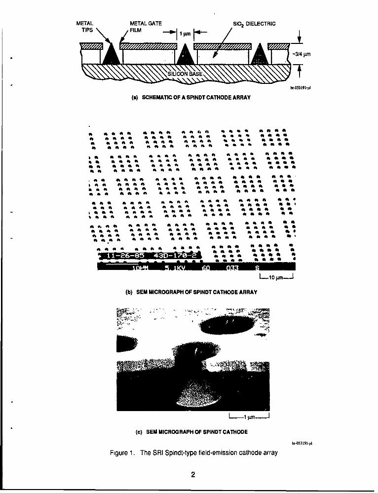
The basic structure for the electron field-emitter array is the Spindt cathode shown inFigure 1. While this particular configuration is ideal for many applications, such as displaydevices, it is not suitable for use as a microwave device. The capacitance of the structure shownis much too large for driving the cathode at frequencies over h -ew hundred kilohertz.
The general expression for the cut-off frequency (ft) is given by ft = gm/ 2nCg where gmis the transconductance and Cg is the capacitance formed by the overlap of the gate and base(emitter) electrodes. To increase ft, we must reduce the capacitance due to this overlap area andincrease gm by increasing the emitter tip density. (It is also possible to increase gm somewhat bydecreasing the operating voltage requirements.)
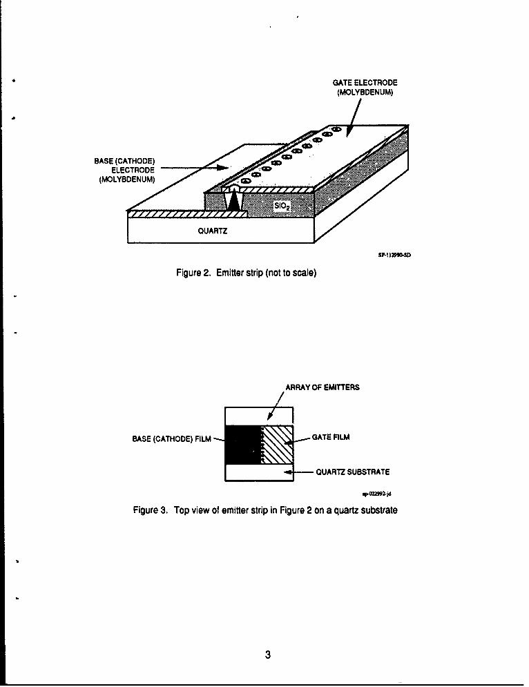
Figure 2 shows a sketch of a low-capacitance, high-tip-density structure that will be thebasic configuration for this development program. The overlap (and therefore the capacitance)of the gate and base electrodes has been kept to a minimum by using a single row of emitters. Afurther decrease of the capacitance may be possible by removing most or all of the SiO2 layer inthe overlap region, thereby reducing the dielectric constant from about 3.8 to about 1.0.
We will construct a simple triode for evaluating the microwave capabilities of such agated cathode by adding an anode mounted on a separate substrate and positioned approximatelya millimeter above the row of emitter tips. The triode structure will be characterized by measur-ing the scattering parameters (S-parameters) of the device using a Hewlett-Packard 8510B net-work analyzer. These parameters will then be used to evaluate the potential of the cathode as amicrowave amplifier and to provide guidance for optimizing the device's performance.
Details of the experimental cathode, its fabrication, and evaluation procedures will bediscussed in the following sections.
2. EXPERIMENTAL CATHODE STRUCTURE
Figure 3 shows a plan view of an emitter strip of the kind shown in Figure 2. The struc-ture will be formed on a square, glass substrate approximately 2.5 x 2.5 mm with a thickness of0.65 mm. The row of emitters will be 1.25 mm long. The base and gate films will be kept asshort as possible (within the constraints of the need to make reliable bonds to the microstriplines) to minimize parasitic circuit elements.
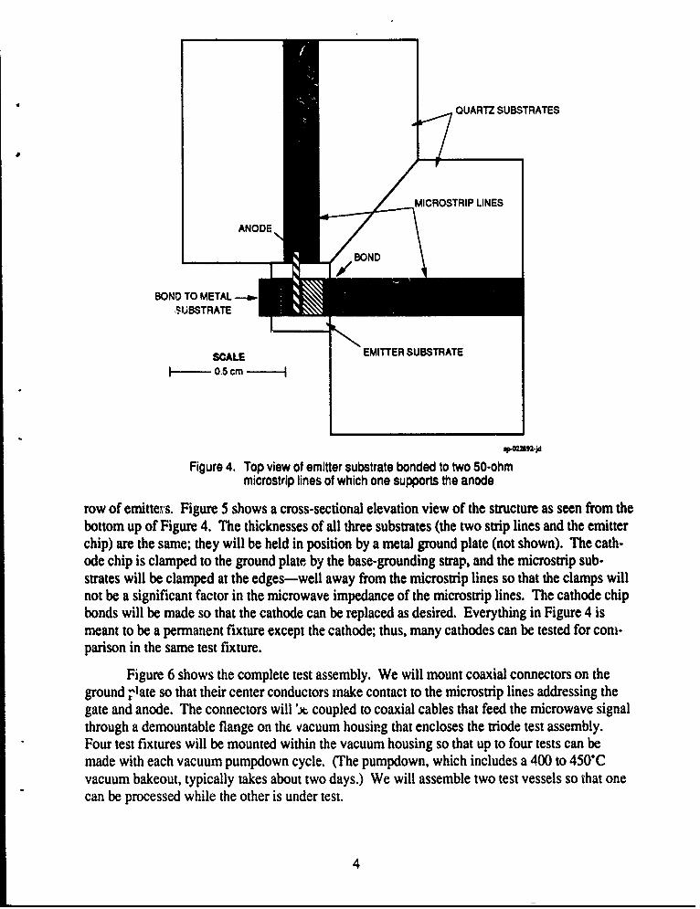
Figure 4 shows a plan view of the complete triode structure with the base electrodebonded to ground, and the gate and anode bonded to 50-ohm microstrip lines. The anodeextends across the emitter chip approximately a millimeter above and slightly to the side of the
METAL METAL GATE S10 2 DIELECTRIC
'-3/4 pim
b.OS3191*jd
(a) SCHEMATIC OF A SPINOT CATHODE ARRAY
~ sft ft5 a~f 556 a5
*5a 4b5 a 45 5 a 5*sa ~ ~ ~ ~ ~ f sft~55 ss C5 .
4f fta 465 0A a 5 * 5
ass sas 05 a5 55
bSS* a~a 55* *55 *aa b
~~s ~ ~ ~ 4 05a Ob5 0a* 065
(b) SEN MICROGRAPH OF SPINDT CATHODE ARRAY
LI .M
(c) SEN MICROGRAPH OF SPINDT CATHODE
bx-053191-jd
Figure 1. The SRI Spindt-type field-emission cathode array
2
GATE ELECTRODE(MOLYBDENUM)
BASE (CATHODE)ELECTRODE
(MOLYBDENUM) W4:
~QUARTZ
Figure 2. Emitter strip (not to scale)
ARRAY OF EMITTERS
BASE (CATHODE) FILM GATE FILM
QUARTZ SUBSTRATE
p-02M.jd
Figure 3. Top view of emitter strip in Figure 2 on a quartz substrate
3
QUARTZ SUBSTRATES
MICROSTRIP LINES
ANODE
BOND TO METAL --UBSTRATE
SCALE EMITTER SUBSTRATE
-0.5 cm
Figure 4. Top view of emitter substrate bonded to two 50-ohmmicrostrip lines of which one supports the anode
row of emittes. Figure 5 shows a cross-sectional elevation view of the structure as seen from thebottom up of Figure 4. The thicknesses of all three substrates (the two strip lines and the emitterchip) are the same; they will be held in position by a metal ground plate (not shown). The cath-ode chip is clamped to the ground plate by the base-grounding strap, and the microstrip sub-strates will be clamped at the edges-well away from the microstrip lines so that the clamps willnot be a significant factor in the microwave impedance of the microstrip lines. The cathode chipbonds will be made so that the cathode can be replaced as desired. Everything in Figure 4 ismeant to be a permanent fixture except the cathode; thus, many cathodes can be tested for com-parison in the same test fixture.
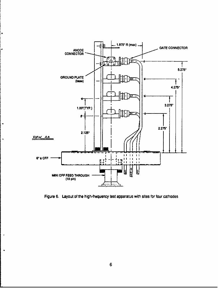
Figure 6 shows the complete test assembly. We will mount coaxial connectors on theground 'late so that their center conductors make contact to the microstrip lines addressing thegate and anode. The connectors will 'x coupled to coaxial cables that feed the microwave signalthrough a demountable flange on the vacuum housing that encloses the triode test assembly.Four test fixtures will be mounted within the vacuum housing so that up to four tests can bemade with each vacuum pumpdown cycle. (The pumpdown, which includes a 400 to 450"Cvacuum bakeout, typically takes about two days.) We will assemble two test vessels so that onecan be processed while the other is under test.
4

ANODE
EMITTER
GATEBASE SiO 2
QUARTZ SUBSTRATE
Figure 5. Cross-sectional view of the structure inFigure 4 seen from the bottom up
Having to work under ultravacuum conditions with the required bakeout complicates thedesign of the test fixture. Ordinary solid-state microwave procedures such as soldering contactsand modifying the circuit during the testing will not be possible. Furthermore, the coaxial cablesand connectors must be able to withstand the 400 to 450'C bakeout. Fortunately, semirigid, her-metically sealed, SiO2-insulated cables and connectors that meet these requirements are commer-cially available (Kaman Industries, Colorado Springs, Colorado).
We plan to make the ground contacts to the microstrip lines by using bump bonding,which will be discussed in Section 3 on fabrication.
3. LOW-CAPACITANCE CATHODE FABRICATION
Figure 7 is a detailed schematic of the cathode concept shown in Figures 2 and 3. Wehave designed and fabricated photomasks for patterning the structure shown; studies of fabrica-tion procedures to achieve the desired cathode geometries are in progress. The photolithographyhas been done with the cooperation of an outside vendor because a sophisticated, specialized, andexpensive photolithography stepper is required to achieve the required dimensions and registra-tion. The dielectric deposition is being done by the outside vendor for the same reasons.
As a first step in the fabrication process, the stepper-lithography vendor checked themasks for alignment specifications by using aluminum metal electrodes; they were found to bewithin specifications. Test structures were then made using our standard electrode material(molybdenum). However, we found that the molybdenum etch normally used for patterningmolybdenum undercut the photoresist excessively for this application. This was not particularlysurprising, because the overlap area is only 4-1im wide in our preferred configuration and even avery small undercut (e.g., 2 gm) can be too much. Unfortunately, it was impossible to controlthe width of the overlap to the desired tolerances using molybdenum, but we have found thatusing the same photolithographic procedures, we can etch chromium films to very well-definededges and tolerances with negligible undercutting. Therefore, chromium was used for the baseelectrode material in fabricating the first test structures. Molybdenum was used for the gate elec-trode because we have a well-developed process for etching precise holes in molybdenum, and
5
1.7'R mxANODEGATE CONNECTOR
CONNECTOR -L
5.275'
GROUND PLATE
4.275*
_-3.275"
2.275'
V1_- W A A
6' 0CFF
Figure 6. Layout of the high-frequency test apparatus with sites for four cathodes
6
652.5 . 1255 iii. 652.5
GOLD U .:
U CONTACTI PAD .'10001341 2605
- LAYER 3 (gate)
LAYER 2 4 or
0.8 pm HOLES . ,A 1264
2 or 5 lpm CENTERS IT 10ISUBSTRATE . ,I
-* 42.5 .1----1275.---.- ..i642.5o -
2560
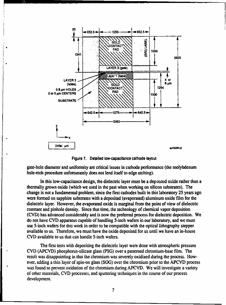
Figure 7. Detailed low-capacitance cathode layout
gate-hole diameter and uniformity are critical issues in cathode performance (the molybdenumhole-etch procedure unfortunately does not lend itself to edge etching).
In this low-capacitance design, the dielectric layer must be a deposited oxdde rather than athermally grown oxide (which we used in the past when working on silicon substrates). Thechange is not a fundamental problem, since the first cathodes built in this laboratory 25 years agowere formed on sapphire substrates with a deposited (evaporated) aluminum oxide film for thedielectric layer. However, the evaporated oxide is marginal from the point of view of dielectricconstant and pinhole density. Since that time, the technology of chemical vapor deposition(CVD) has advanced considerably and is now the preferred process for dielectric deposition. Wedo not have CVD apparatus capable of handling 5-inch wafers in our laboratory, and we mustuse 5-inch wafers for this work in order to be compatible with the optical lithography stepperavailable to us. Therefore, we must have the oxide deposited for us until we have an in-houseCVD available to us that can handle 5-inch wafers.
The first tests with depositing the dielectric layer were done with atmospheric pressureCVD (APCVD) phosphorus-silicate glass (PSG) over a patterned chromium-base film. Theresult was disappointing in that the chromium was severely oxidized during the process. How-ever, adding a thin layer of spin-on glass (SOG) over the chromium prior to the APCVD processwas found to prevent oxidation of the chromium during APCVD. We will investigate a varietyof other materials, CVD processes, and sputtering techniques in the course of our processdevelopment.
7
As part of the deposition process development, we fabricated structures to test compati-bility with the cone formation process. The first test structures for this purpose consisted of apatterned chromium-base film, an APCVD dielectric layer of PSG, and a molybdenum gate filmpatterned with a row of holes along the edge of the base film as shown in Figure 7. The gateelectrode shape is patterned as a last step after the cones are in place. The base and gate filmswere deposited at SRI, and the APCVD PSG dielectric layer was deposited by the vendor.
The standard molybdenum cone formation process was performed on the structure, andthe aluminum/alumina sacrificial parting layer was etched off using one of our standard partinglayer etchants, potassium hydroxide (KOH). We used KOH because our usual parting layeretchant, phosphoric acid, attacks chromium which was used as the base film in these structures.(Much of our prior work has been on silicon substrates; there, KOH can be used only briefly,because it attacks silicon rapidly.)
The result of this first cone formation test was disappointing in that the PSG layer did nothold up to the KOH, and the gate film was undercut excessively during the etch-off of the sacri-ficial layer. This was a surprise, because KOH should not attack PSG so vigorously. Closeinspection of the structure showed that the molybdenum gate film did not adequately protect thePSG film because of a roughness of the PSG layer that led to vias in the overlaying molybdenumfilm. The vias are due to poor "step coverage" of the rough features on the PSG surface becauseof the highly directional nature of the evaporation process used to deposit the molybdenum. Weare confident that the excessive roughness of the PSG layer is abnormal and can be greatlyimproved. It is likely that this first trial PSG deposition was, for some reason, out of specifica-tion, leading to poor stoichiometry and surface roughness. The roughness led to pinholes thatexposed the PSG to the KOH, and the poor stoichiometry led to the excessive KOH etch rateFigure 8 shows an electron micrograph and schematic of this low-capacitance structure with thedielectric layer overetched and the gate film broken away from large areas as a result.
Subsequent experiments have produced improved dielectric layers, although some diffi-culties are still being experienced with breakup of the PSG layer. Nevertheless, some low-capacitance cathode structures have been fabricated that were good enough to attempt electricaltests, and some very encouraging results have been obtained. These are discussed in Section 4.Different metals, dieleetric materials (e.g., borophosphosilicate glass or BPSG and Si0 2), anddeposition procedures will be investigated during ongoing studies of the fabrication processes.In addition, SRI has obtained a sputtering system capable of depositing metal and dielectriclayers on 5-inch wafers, and this will be on-line and available for material studies shortly.
8

MOLYBDENUM GATE
p/
CHROMIUM BASE
Figure 8. SEM and cross-section of a portion of a low-capacitancecathode structure with the dielectric layer undercut so that thegate film lifted and broke away from a large area
4. CATHODE EMISSION TESTS
Cathode emission tests have been carried out in three study areas: (1) how to achievestable performance with close-spaced anodes, (2) means for lowering the operating voltagerequirements, and (3) the performance of the low-capacitance cathode structures now underdevelopment.
4.1 CLOSE-SPACED ANODES
In work done prior to this project, it was shown tLt the field-emitter arays are capable ofup to at least 1000 A/cm2 of emission (Spindt et al., 1991), and that tip loadings of at least500 pA/tip are possible (Spindt et al., 1984). In general, our experience with probing these high-performance regimes has shown that limitations on performance are more often associated withpower dissipation at the collector than with the ability of the emitter array to produce emission.Having to work with small, close-spaced anodes can be a severe problem with regard to powerhaadling, outgassing, and arcover, unless the anodes are of the proper material and very carefullyprocessed.
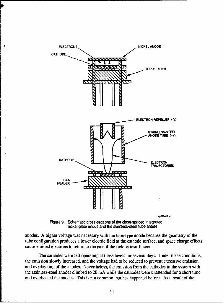
In an effort to learn more about the effects of close-spaced collectors, collector materials,and collector processing on the performance of the emitter arrays, we mounted three cathodeshaving 1000 tips in an area 256- x 256-m square (packing density of 1.5 x 10⁶ tips/cm2) in eachof two test vessels. One test vessel was used as a contil and was fitted with our often-used3/8-inch-diameter 304 stainless-steel tube anodes and mounted about 3 mm from the cathodes sothat the electron beam was emitted down the bore of the tube. The second test vessel wasequipped with small nickel-plate anodes mounted on the TO-5 header with the cathodes. Thenickel-plate anodes are parallel to the cathode chips and about 1 mm from the cathodes. The twotypes are shown in Figure 9. In each case, the anodes were pretreated in the same way that theanodes used in our traditional test systems are prepared: the anodes were chemically cleaned,hydrogen fired at 1400K for one-half hour, and then heated in vacuum by electron bombardmentuntil all evidence of outgassing disappeared.
The vessel with stainless-steel tube anodes was capable of handling more power than theTO-5-mounted nickel-plate anodes because of the larger area of the tube-shaped anode. In addi-tion, the close spacing between the TO-5-mounted nickel-plate anode and the cathode (= 1 mm)increases the power density to the nickel-plate anode because the electron beam doesn't havespace to spread out before impacting the anode. Pumpout of any gas evolved from the nickel-plate anode was also restricted by the close spacing.
After pumpdown and bakeout, the emission level was brought up to 10 mA from eachcathode with nickel-plate anodes using a 60-Hz half-wave driving voltage (20% duty cycle) and180 V on the anode. The cathodes in the test vehicle with the stainless-steel anodes were alsoslowly increased in emission up to 10 mA with the 60-Hz half-wave drive, but with 600 V on the
10
ELECTRONS NICKEL ANODE
CATHODE
TO-5 HEADER
ELECTRON REPELLER (-V)
STAINLESS-STEELANODE TUBE (+V)
CATHODEELECTRONTRAJECTORIES
TO-5HEAUER "
W.OZ692-jd
Figure 9. Schematic cross-sections of the close-spaced integratednickel-plate anode and the stainless-steel tube anode
anodes. A higher voltage was necessary with the tube-type anode because the geometry of thetube configuration produces a lower electric field at the cathode surface, and space charge effectscause emitted electrons to return to the gate if the field is insufficient.
The cathodes were left operating at these levels for several days. Under these conditions,the emission slowly increased, and the voltage had to be reduced to prevent excessive emissionand overheating of the anodes. Nevertheless, the emission from the cathodes in the system withthe stainless-steel anodes climbed to 20 mA while the cathodes were unattended for a short timeand overheated the anodes. This is not common, but has happened before. As a result of the
11

excessive heating of the anodes, an electrical leakage developed between the base and gate filmsof all three cathodes in the stainless-steel anode system. It is not clear at this time whether theleakage was due to evaporation of material from the stainless steel onto the cathodes, overheating
of the cathodes, overheating of the TO-5 cathode mounts, or some combination of these possi-bilities. During subsequent operation, the leakage continued to increase, and the voltage requiredto maintain emission also increased slowly with time. Eventually, one of these cathodes failed toa short circuit. The other two cathodes were then held at 10 mA peak emission and shown to bestable at that level for 4 weeks, at which time they were shut down. Figure 10 is a plot of theemission current vs. the reciprocal of the applied voltage for the remaining two cathodes (53i-300-8Q and 53i-300-8T) in the stainless-steel-anode vessel just prior to shutdown.
10-1 E - - -ii~ !!ii~ii~~~~iii!~i!i~iiiiiiiii::
................... .................. 4.................. .4,................. . ................. ..................
..................... ... ................. .................. ..................IIZZIZ
10-2
IE - ............... . . . . . . .... . ....................... ... .-.... ~. .. ........ .3.0-0
.................... .53308............... ............
4 5 6 7 8 9 10
1000N,So3o192id
Figure 10. Emission data for 53i-300-8Q and 53i-300-8T(1000 emitter tips)
An important point to make is that the results described above are essentially identical tothose obtained in an earlier experiment with the same apparatus except that 10,000-tip arrayswere used. It seems clear that the performance limits are due to anode loading rather than cath-ode loading, and that the cathodes may well be capable of much higher performance than weusually observe because of power dissipation limitations with the collectors in most of the testset-ups.
12
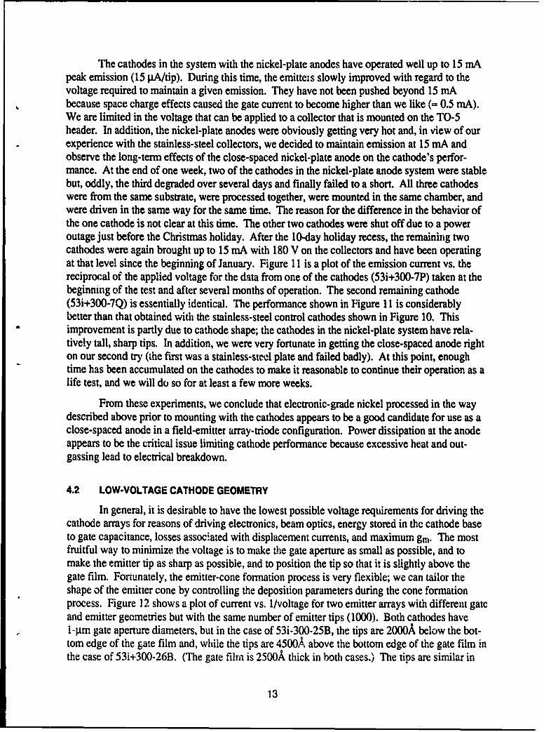
The cathodes in the system with the nickel-plate anodes have operated well up to 15 mApeak emission (15 pA/tip). During this time, the emitteis slowly improved with regard to thevoltage required to maintain a given emission. They have not been pushed beyond 15 mAbecause space charge effects caused the gate current to become higher than we like (= 0.5 mA).We are limited in the voltage that can be applied to a collector that is mounted on the TO-5header. In addition, the nickel-plate anodes were obviously getting very hot and, in view of ourexperience with the stainless-steel collectors, we decided to maintain emission at 15 mA andobserve the long-term effects of the close-spaced nickel-plate anode on the cathode's perfor-mance. At the end of one week, two of the cathodes in the nickel-plate anode system were stablebut, oddly, the third degraded over several days and finally failed to a short. All three cathodeswere from the same substrate, were processed together, were mounted in the same chamber, andwere driven in the same way for the same time. The reason for the difference in the behavior ofthe one cathode is not clear at this time. The other two cathodes were shut off due to a poweroutage just before the Christmas holiday. After the 10-day holiday recess, the remaining twocathodes were again brought up to 15 mA with 180 V on the collectors and have been operatingat that level since the beginning of January. Figure 11 is a plot of the emission current vs. thereciprocal of the applied voltage for the data from one of the cathodes (53i+300-7P) taken at thebeginning of the test and after several months of operation. The second remaining cathode(53i+300-7Q) is essentially identical. The performance shown in Figure 11 is considerablybetter than that obtained with the stainless-steel control cathodes shown in Figure 10. Thisimprovement is partly due to cathode shape; the cathodes in the nickel-plate system have rela-tively tall, sharp tips. In addition, we were very fortunate in getting the close-spaced anode righton our second try (the first was a stainless-steel plate and failed badly). At this point, enoughtime has been accumulated on the cathodes to make it reasonable to continue their operation as alife test, and we will do so for at least a few more weeks.
From these experiments, we conclude that electronic-grade nickel processed in the waydescribed above prior to mounting with the cathodes appears to be a good candidate for use as aclose-spaced anode in a field-emitter array-triode configuration. Power dissipation at the anodeappears to be the critical issue limiting cathode performance because excessive heat and out-gassing lead to electrical breakdown.
4.2 LOW-VOLTAGE CATHODE GEOMETRY
In general, it is desirable to have the lowest possible voltage requirements for driving thecathode arrays for reasons of driving electronics, beam optics, energy stored in the cathode baseto gate capacitance, losses associated with displacement currents, and maximum gm. The mostfruitful way to minimize the voltage is to make the gate aperture as small as possible, and tomake the emitter tip as sharp as possible, and to position the tip so that it is slightly above thegate film. Fortunately, the emitter-cone formation process is very flexible; we can tailor theshape of the emitter cone by controlling the deposition parameters during the cone formationprocess. Figure 12 shows a plot of current vs. I/voltage for two emitter arrays with different gateand emitter geometries but with the same number of emitter tips (1000). Both cathodes have1-pn gate aperture diameters, but in the case of 53i-300-25B, the tips are 2000A below the bot-tom edge of the gate film and, while the tips are 4500A above the bottom edge of the gate film inthe case of 53i+300-26B. (The gate film is 2500A thick in both cases.) The tips are similar in
13
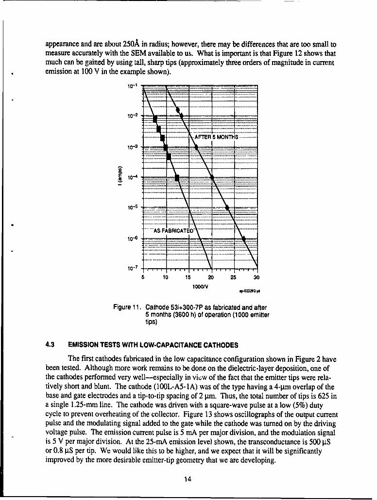
appearance and are about 250A in radius; however, there may be differences that are too small tomeasure accurately with the SEM available to us. What is important is that Figure 12 shows thatmuch can be gained by using tall, sharp tips (approximately three orders of magnitude in currentemission at 100 V in the example shown).
10-1 {.::':,:'.. "':.'L:.&:::':::::"F:.::::':.::::: ,:.,
....- ... .... ..... ......... {.............R ........... ....
10-2 1: .. . ....... ............ f.
E ,o-, .
...... ........ .......... .... ........... ....... .................. ............ .....::::
ic- 5 . . . . . . ... ..........
. . .. ...........I ........... ......... . .10-8 .. ....... ........... ... ~. ..........
10-3.. .
Figure 11. Cathode 53i+300-7P as fabricated and after5 months (3600 h) of operation (1000 emittertips)
4.3 EMISSION TESTS WITH LOW-CAPACITANCE CATHODES
The first cathodes fabricated in the low capacitance configuration shown in Figure 2 havebeen tested. Although more work remains to be done on the dielectric-layer deposition, one of
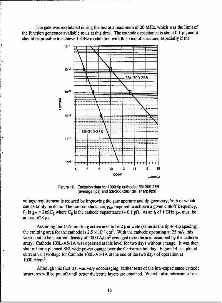
the cathodes performed very well--especially in view of the fact that the emitter tips were rela-tively short and blunt. The cathode (100L-A5-1A) was of the type having a 4-itm overlap of thebase and gate electrodes and a tip-to-tip spacing of 2 I tn. Thus, the total number of tips is 625 ina single 1.25-mm line. The cathode was driven with a square-wave pulse at a low (5%) dutycycle to prevent overheating of the collector. Figure 13 shows oscillographs of the output currentpulse and the modulating signal added to the gate while the cathode was turned on by the drivingvoltage pulse. The emission current pulse is 5 mA per major division, and the modulation signalis 5 V per major division. At the 25-mA emission level shown, the transconductance is 500 itSor 0.8 ~iS per tip. We would like this to be higher, and we expect that it will be significantlyimproved by the more desirable emitter-tip geometry that we are developing.
14
The gate was modulated during the test at a maximum of 20 MHz, which was the limit ofthe function generator available to us at this time. The cathode capacitance is about 0.1 pf, and itshould be possible to achieve 1 -GHz modulation with this kind of structure, especially if the
10-1.
10-2 - _ _ _
- -- 53i+300-26B
............................... . .. . ............. ................... ... ....... ..........
........................................ ......2*B....... .............
1 0 -4 .. ..-I .. .. ... ... . .... .... ...
10 12 14 16 18
IO00/V
Figure 12. Emission data for 1000-tip cathodes 53i-300-25B(average tips) and 53i-300-26B (tall, sharp tips)
voltage requirement is reduced by improving the gate aperture and tip geometry, 'both of whichcan certainly be done. The transconductance, gin, reqluired to achieve a given cuttoff frequency,ft, is gm = 2 tftCg where Cg is the cathode capacitance (-- 0.1l pf). At an ft of 1 GHz gm must beat least 628 jis.
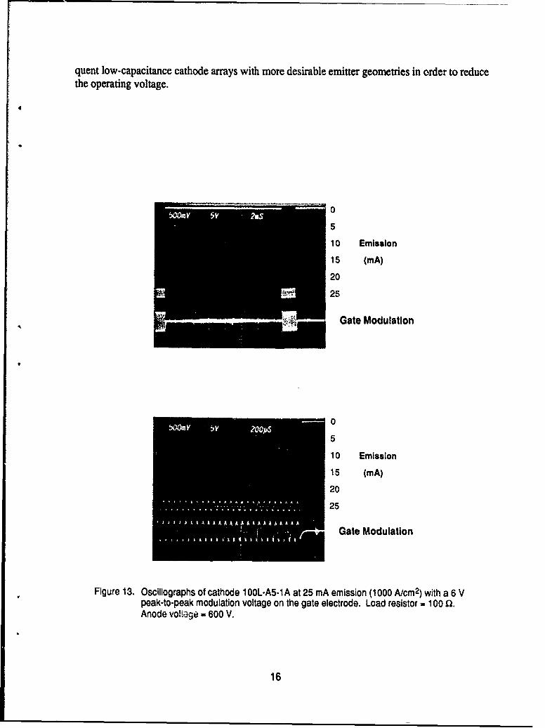
Assuming the 1.25-mm-long active area to be 2 I±m wide (same as the tip-to-tip spacing),the emitting area for the cathode is 2.5 x 10"5 cm2. With the cathode operating at 25 mA, thisworks out to be a current density of 1000 A/cm2 averaged over the area occupied by the cathodearray. Cathode 100L-A5-1A was operated at this level for two days without change. It was thenshut off for a planned SRI-wide power outage over the Christmas holiday. Figure 14 is a plot ofcurrent vs. 1/voltage for Cathode 100L-A5-1IA at the end of the two days of operation at1000 A/cm2.
Although this first test was very encouraging, further tests of the low-capacitance cathodestructures will be put off until better dielectric layers are obtained. We will also fabricate subse-
15
quent low-capacitance cathode arrays with more desirable emitter geometries in order to reducethe operating voltage.
5
10 Emissionis (mA)
20
25
j Gate Modulation
Il
0
510 Emission
15 (mA)
20
25
.. Gate Modulation
Figure 13. Oscillographs of cathode 10OL-A5-IA at 25 mA emission (1000 A/cm 2) with a 6 Vpeak-to-peak modulation voltage on the gate electrode. Load resistor = 100 Q.
Anode vol,-ge = 600 V.
16

10-1I' J . 0007- i ii i"!
10-2
io-, ti .
.. ... .... ... -." .... .. .... . ... ..
*~1- 4 _67L 9 1
10-4 ""i .. .. i... .. "i .... ... ..... .... ... .... ... ..., " . ... .. .... ... .. . ... ."r"' ...
catho.de ; 100-A1 up to 100 A/cm
10 -5 " . ".. ".. ... .... .. ..... .. ... . ... ... .'" ... ....... .. .. -.
IO " ........ ; ... ... , .!.. ... .... ...... ; ... . ,. ...... ... ... ...
:::::::: :::::::::::::: :::... .. ... ...... ... .
Ac6 icrowav d s. ....... a... ... ...l....... ....... d ... r....s. ........... u
demonstrationof... ... t... aity om d l...e ...ei on t .... ... ...i is csa....... t e
Fi5r6 7 w d f p
1000/V
FiGure14. Current vs. I/voltage plot for low-capacitancecathode I OOL-A5-1 A up to 1000 A/cm 2
5. MICROWAVE MEASUREMENTS
Active microwave devices, such as FETs and bipolar semiconductors, are usually char-acterized by measuring their S-parameters which provide a complete picture of their potentialperformance in all microwave applications. Although the present contract calls only for ademonstration of the ability to modulate emission at I GHz, it is necessary to measure theS-parameters of the device in order to eliminate all ambiguities. The test fixture shown inFigure 6 was designed for this purpose.
Working at I GHz requires that the emitter be operated at a current sufficiently high toprovide a significant transconductance. Because this will require working at a high current den-sity (estimated to be a few hundred amps/cm 2) and an emitter-anode voltage in the range of 100to 200 V to overcome space-charge effects, power densities to be dealt with at the anode will berather large (in the 50 W/cm 2 range). So much power would require a heat-sink at the anode,
17
which would be a troublesome complication at this stage of development. An alternative is touse pulsed measurements to explore the high-performance region; this is what will be done forthese first experiments. The measurements will be performed with the HP 8510B network ana-lyzer which allows pulsed microwave measurements (Hewlett-Packard, 1988). At present, weare testing the pulsed measurement procedures on known microwave elements.
Characterizing devices on the network analyzer requires calibration measurements thatremove the effects of the coupling fixtures and the network analyzer itself on the measurements.For the purposes of calibration, three calibration fixtures will be needed for the standard so-called Thru-Reflect-Line (TRL) calibration used for noncoaxial measurements (Hewlett-Packard,1987). The calibration fixtures will be similar to those discussed in connection with Figure 4.For the "thru" measurement, the two microstrip lines will be lined up and connected together.The "reflect" measurement requires a short-circuit at the end of the two lines; the "line" mea-surement is identical to the "thru" measurement but with a quarter-wavelength-long line added tothe connected lines. When all the S-parameters have been measured, we can easily evaluate theuse of the triode as, for example, an amplifier. The general expression for the transducer gain,GT, i.e., the ratio of the power delivered to the load and the power available from the source, isgiven by
I(I -S11 rsl( -S22 rL)-S21 S12 US
where rS and FL are the reflection coefficients at the source and load respectively. The generalexpression for the ieflecdion coefficient is
-= .- Z(2)
where Z is usually the 50-ohm line impedance and Z, the impedance at port i. In the simplercase where the power reflected back from the load to the input given by IS 1212 is zero, Gr sim-plifies to the unilateral transducer gain given by
S-IrsF xIS2 rx 1-I1rP ()1-s,,Irsf I-S22 Ilr (3
GTU thus consists of the product of three factors: the first presents the effect of impedance mis-match at the input; the last presents a similar mismatch at the output; and the second, 1S1212, is thepower gain of the active device provided through its transconductance. Entering the experimen-tal values in these equations will clearly show which factors limit the gain and what can be doneto reduce their effect. Matching at the input and output (Cs = $t1, FL = S ) maximizes the gainto
= nI S21 12
18

For absolute stability of the amplifier with a passive source and load impedance, the followingconditions must be met
IS1 I< 1, S22 < 1 (5a)
IS12S21 I-IM*'1(5b
I SnF IFI 12
where
D = St S22 - S12 S21 (6a)
M = S22 - D S. (6b)
N=S22-DS 1 . (6c)
6. WORK PLANNED
During the next period, we will begin fabrication of the microwave test vehicle and con-tinue the development of the low-capacitance cathode structure. In addition, we will continue tostudy methods to further reduce the voltage requirements for emission.
REFERENCES
Holland, C.E., A. Rosengreen, and C.A. Spindt, 1991: "A Study of Field Emission Micro-triodes," IEEE Trans. Elec. Dev. 38(10), October.
Hewlett-Packard, 1988: HP 8510B Network Analyzer: "Introductory Pulsed RF-MeasurementsUser's Guide," HP Part No. 08810-90183, Hewlett Packard, December.
Hewlett-Packard, 1987: "Applying the HP 8510B TRL Calibration for Non-Coaxial Measure-ments," HP Product Note 8510-8, Hewlett Packard, October.
Hewlett-Packard, 1968: "S-Parameters.. .Circuit Analysis and Design," HP Applications Note95, Hewlett Packard, 3-12, September.
19
Spindt, C. A., C.E. Holland, and R.D. Stowell, 1984: "Recent progress in low-voltage field-emission cathode development," J. de Phys. Comp. C9, Supp. to Vol. 45, No. 12, 269,December.
Spindt, C. A., C.E. Holland, A. Rosengreen, and I. Brodie, 1991: "Field-emitter arrays forvacuum microelectronics," IEEE Trans. on Elec. Devices 38(10), October.
K
20