resonant tunneling of electrons in quantum wiresapalev/lowtempkrive2010.pdf73.23.hk coulomb...
TRANSCRIPT

© I.V. Krive, A. Palevski, R.I. Shekhter, and M. Jonson, 2010
* Also at the Division of Quantum Phases and Devices, School of Physics, Konkuk University, Seoul 143-701, Korea
Fizika Nizkikh Temperatur, 2010, v. 36, No. 2, p. 155–180
Resonant tunneling of electrons in quantum wires (Review Article)
I.V. Krive1,2, A. Palevski3, R.I. Shekhter1, and M. Jonson1,4* 1Department of Physics, University of Gothenburg, SE-412 96 Göteborg, Sweden
2B. Verkin Institute for Low Temperature Physics and Engineering of the National Academy of Sciences of Ukraine 47 Lenin Ave., Kharkov 61103, Ukraine
E-mail: [email protected]
3Tel Aviv University, School of Physics and Astronomy, IL-69978 Tel Aviv, Israel 4School of Engineering and Physical Sciences, Heriot Watt University, Edinburgh, EH14 4AS, Scotland, UK
Received July 14, 2009
We considered resonant electron tunneling in various nanostructures including single wall carbon nanotubes, molecular transistors and quantum wires formed in two-dimensional electron gas. The review starts with a text-book description of resonant tunneling of noninteracting electrons through a double-barrier structure. The effects of electron–electron interaction in sequential and resonant electron tunneling are studied by using Luttinger liq-uid model of electron transport in quantum wires. The experimental aspects of the problem (fabrication of quan-tum wires and transport measurements) are also considered. The influence of vibrational and electromechanical effects on resonant electron tunneling in molecular transistors is discussed.
PACS: 73.63.–b Electronic transport in nanoscale materials and structures; 73.23.Hk Coulomb blockade; single-electron tunneling; 85.85.+j Micro- and nano-electromechanical systems (MEMS/NEMS) and devices.
Keywords: nanostructures, two-dimensional electron gas, quantum tunneling, fabrication of quantum wires.
Contents 1. Introduction .......................................................................................................................................... 156 2. Resonant tunneling of noninteracting electrons ................................................................................... 157
2.1. Landauer–Büttiker approach and the Breit–Wigner formula. ...................................................... 157 2.2. Sequential electron tunneling and 1/T-scaling of conductance ..................................................... 158
3. Effects of electron–electron interaction ................................................................................................ 159 3.1. Coulomb blockade and conductance oscillations. ........................................................................ 159 3.2. The Meir–Wingreen formula ........................................................................................................ 159 3.3. Sequential tunneling through a Luttinger liquid quantum dot ...................................................... 160 3.4. Resonant tunneling in a Luttinger liquid ...................................................................................... 162 3.5. Long-range quantum coherence in a chiral Luttinger liquid. ........................................................ 163
4. Electron transport in single-wall carbon nanotubes and quantum wires in confined 2DEGs (expe-riment) ................................................................................................................................................. 165 4.1. Fabrication of GaAs quantum wires. ............................................................................................ 166 4.2. Deviation of the 1D conductance from the conductance quantum at low temperatures ............... 167 4.3. Carbon nanotubes ......................................................................................................................... 168 4.4. Resonant tunneling in GaAs quantum wires and SWNTs ............................................................ 168
5. Vibrational effects in resonant electron transport ................................................................................. 170 5.1. Electron transport through a vibrating quantum dot. The model .................................................. 171 5.2. Phonon-assisted electron tunneling and polaronic effects ............................................................ 172 5.3. Electron shuttling. ........................................................................................................................ 174 5.4. Electron tunneling through nano-electromechanical systems. ...................................................... 176
6. Conclusion ........................................................................................................................................... 177 Acknowledgments .................................................................................................................................... 178 References. ............................................................................................................................................... 178

I.V. Krive, A. Palevski, R.I. Shekhter, and M. Jonson
156 Fizika Nizkikh Temperatur, 2010, v. 36, No. 2
1. Introduction
The concept of quantum tunneling was introduced in physics in 1928 in two theoretical papers: by G. Gamow (who also invented the term quantum tunneling) for solv-ing the problem of α-decay in nuclear physics [1], and by R.H. Fowler and L.W. Nordheim in their seminal paper on field emission [2]. The experiments on emission of elec-trons from metals in intense electric fields were the first to verify the phenomenon of quantum tunneling (see, e.g., [3]). The mere fact that the concept of quantum tunneling appeared in the very beginning of the «quantum mechani-cal era» and simultaneously in two different regions of physics showed the generality and fundamental character of the novel phenomenon.
Quantum tunneling is the term introduced to describe the quantum evolution of a system in classically forbidden domains of configurational (or real) space. The very exis-tence of tunneling is entirely due to the Heisenberg uncer-tainty principle, which allows one to consider virtual processes. In the path integral approach the tunneling is described by «trajectories» in imaginary time and their contribution is exponentially small if the corresponding action tS . In this sense tunneling is a more simple process than quantum evolution in real time, where the superposition of different quantum states makes the dy-namics complicated and intricate. One can consider the tunneling of single particles, composite objects, phase states (vacuum-to-vacuum tunneling in quantum field theory and macroscopic quantum tunneling in condensed matter physics) and even the tunneling of the Universe as a whole (in quantum cosmology). In modern physics quan-tum tunneling is considered as one of the basic quantum phenomena, inherent in quantum dynamics.
As a rule the probability of quantum tunneling is small. (Nevertheless it is the main effect when the classical pro-cesses are energetically forbidden.) In most cases the tun-neling probability depends exponentially on the parameters of the effective (or real) potential barrier the system tun-nels through. A special type of tunneling takes place if the quantum transition couples more than two classically al-lowed states. For instance, one can consider the complex process involving two tunneling transitions connecting the initial and final states of evolution with an intermediate classically allowed state. For such transitions the quantum phase coherence should play a crucial role. The tunneling probability is radically changed when the phase coherence is preserved. It is strongly enhanced for constructive inter-ference, when it gives rise to the phenomenon known as resonant tunneling (first introduced by G. Breit and E. Wigner in their theory of slow neutron capture [4]).
The simplest and most important example of resonant tunneling is a single-particle transition through a double barrier, in the case when the tunneling through each indi-vidual barrier is weak and one can consider a set of well defined resonance states in a potential well between the barriers (see, e.g., [5]). In a single particle scattering theory
the transition probability at energies around the resonant state energy is described by the Breit–Wigner distribution function characterized by the energy 0ε and the width Γ of the resonance state (the ratio 0/ 1Γ ε for pronounced resonant behavior). The intensity of non-resonant transi-tions is proportional to 2Γ . For tunneling events when the energy of the scattering particle falls in an energy window of width Γ around the resonance level, the transition pro-bability ceases to depend on Γ for symmetric barriers. This fully coherent tunneling process is usually referred to as resonant quantum tunneling (RQT). RQT has to be dis-tinguished from the very important resonant process called sequential tunneling (ST) when electrons incoherently tun-nel to and from the intermediate real state. The probability of ST (∝Γ ) is much larger than that for non-resonant transitions ( 2∝ Γ ) and the differential conductance peaks at voltages equal to the energies of intermediate states. However, for given transparencies of the individual bar-riers, ST can be regarded as a classical process. It is inter-esting to notice, however, that in the lowest order of per-turbation theory in Γ the calculations based on fully quan-tum-mechanical approaches (for instance, on the Landau-er–Büttiker approach) lead to the same results as calcula-tions performed using classical methods (the master equa-tion approach).
The aim of this review article is to discuss different as-pects of electron resonant transport (coherent and incohe-rent) in modern nanoelectrical (and nanoelectromecha-nical) devices: quantum wires (including single-wall car-bon nanotubes), single electron transistors and molecular junctions. We consider the main effects in electron tunne-ling in these devices (Coulomb blockade, Luttinger liquid effects, vibrational effects, electron shuttling) and review experimental observations of these phenomena.
We start (Sec. 2) with a text-book description of reso-nant transitions of noninteracting electrons through a double barrier system (single-level quantum dot weakly coupled to the leads) by using two different approaches: (i) the Landauer–Büttiker scattering theory (a fully quantum-mechanical description), and (ii) the «master equation» approach (a classical description). In high-temperature region T Γ both approaches give the same result. In particular, a so-called 1/T-scaling (T is the temperature) of the maximum peak conductance is predicted. Recently this simple prediction was tested in experiments on carbon na-notube-based quantum dots (see, e.g., [6]).
The influence of the electron–electron interaction on re-sonant tunneling is considered in Sec. 3. This problem has in recent years attracted a particularly strong interest from theoreticians. Transport properties of single-wall carbon nanotubes (SWNT) are known (see, e.g., [7]) to be de-scribed by Luttinger liquid (LL) theory. The experiment [9] on a doubly buckled SWNT, which was supposed to behave as a double-barrier Luttinger-liquid system, showed disagreement with predictions of the LL model. This ob-servation stimulated theoreticians to reconsider the reso-nant tunneling in a LL using different approaches. We dis-

Resonant tunneling of electrons in quantum wires
Fizika Nizkikh Temperatur, 2010, v. 36, No. 2 157
cuss in Sec. 3 how electron–electron correlations influence the temperature dependence of the conductance and, in particular, how LL effects modify the «1/T-scaling» of the maximum conductance for sequential electron tunneling (T Γ).
For quantum resonant tunneling (T Γ ) the conduc-tance of a fully symmetric junction, as was already shown in the seminal paper by Kane and Fisher [8], is not renor-malized by the interaction and coincides with the conduc-tance quantum as 0T → . The presence of asymmetry changes drastically the low-T asymptotic behavior of the conductance — it scales to zero [8]. In the general case of asymmetric junctions, a non-monotonic dependence of the conductance on temperature (with a pronounced maximum at T Γ∼ ) is the signature of LL effects in quantum reso-nant tunneling. So far this specific behavior has not been observed in experiments.
In Sec. 4 experiments on electron transport through quantum wires are discussed.
Electron transport in nanodevices is affected not only by Coulomb effects but in special cases (molecular junc-tions, suspended nanotubes) by vibrational effects as well (Sec. 5). This area of research is connected with the rela-tively old field of inelastic electron tunneling spectroscopy (including point-contact spectroscopy [10]) and with novel physics — nanoelectromechanics. Vibrational effects may either enhance electron transport due to contributions from additional inelastic channels or suppress the charge current because of polaronic effects. The interplay of polaronic effects and vibron-assisted tunneling could result in an anomalous (non-monotonic) temperature dependence of the conductance in the regime of sequential electron tunne-ling. A spectacular positive (strong enhancement of cur-rent) influence of vibrational effects on electron tunneling is demonstrated by the phenomenon of electron shuttling (see the review [11]). In Sec. 5.3 we consider the shuttle instability (that is the conditions at which the system un-dergoes a transition to a new shuttle-like regime of electron transport) for the case of a single-electron transistor in the regime of strong electromechanical coupling. Experiments where nano-electromechanical effects have been observed are discussed in Sec. 5.4.
In the Conclusion section the perspectives for the de-velopment and applications of this novel area of research are discussed.
2. Resonant tunneling of noninteracting electrons
We start by considering the simplest possible theoretical model of resonant electron transport in metallic structures. This model describes a one-dimensional double-barrier structure connected to reservoirs of noninteracting electrons. Electron transport inside the structure is assumed to be phase-coherent and ballistic. The left (L) and right (R) elec-tron reservoirs (leads) are characterized by equilibrium dis-tribution functions
1( , ) = exp( / ) 1j j jf T T
−⎡ ⎤μ ε −μ +⎣ ⎦
where T is temperature and ( = , )j j L Rμ are the chemi-cal potentials ( = L ReV μ −μ is the driving voltage).
2.1. Landauer–Büttiker approach and the Breit–Wigner formula
The Landauer–Büttiker approach [12] (see also Ref. 13) relates the average current through the system to the transmission coefficient (probability) ( )tT ε for an electron emerging with energy ε from the reservoir to traverse the structure («conductance is transmission» [14])
0
2( ) = ( )[ ( ) ( )].t L ReJ V d T f f
h
∞ε ε ε − ε∫ (1)
In the linear response regime, 0V → , one readily gets from Eq. (1) the famous Landauer formula for the conduc-tance = /G J V ,
00
( ) = ( ) ,tfG T G d T
∞ ∂⎛ ⎞ε ε −⎜ ⎟∂ε⎝ ⎠∫ (2)
where 20 = 2 /G e h is the conductance quantum (the fac-
tor 2 is due to spin projection degeneracy) and / =f−∂ ∂ε 2= 1/ 4 cosh [( ) / 2 ]T Tε −μ .
For weak tunneling (small barrier transparencies) the electron energies in the well form a discrete set of broa-dened levels = / 2n n tE iε − Γ , where =t L RΓ Γ +Γ is the level width ( tΓ δε , where δε is the characteristic level spacing). The transmission coefficient for the double-barrier structure resonances near =r nε ε and it is well approximated by the Breit–Wigner formula (see, e.g., [5])
2 2( ) = .( ) ( / 2)
L RBW
r tT
Γ Γε
ε − ε + Γ (3)
The total level width tΓ determines the decay rate, /tΓ , of the resonant state; the partial widths =j jDΓ ν are determined by the barrier transparencies 1jD and the attempt frequency ( ),rν ε which for rectangular barriers is
= 2 / ( ),rL vν ε where L is the distance between the bar-riers and ( )rv ε is the electron velocity at the resonance energy.
For an energy-independent level width in Eq. (3), the integral in Eq. (1) can be evaluated exactly. The result can be expressed in terms of the psi-function ( ( )xψ ≡
ln ( ),x x≡ ∂ Γ where ( )xΓ is the gamma-function). By using an integral representation of the imaginary part of ψ-function,
1Im =2
x iy⎛ ⎞ψ + +⎜ ⎟⎝ ⎠
2 2 ( ) 2 ( )
0
1 1= ,1 e 1 e 1xt y xt y
dtt
∞
π − π +⎡ ⎤
−⎢ ⎥+ + +⎣ ⎦
∫ (4)
one readily represents the current of noninteracting elec-trons through a resonant level as
I.V. Krive, A. Palevski, R.I. Shekhter, and M. Jonson
158 Fizika Nizkikh Temperatur, 2010, v. 36, No. 2
= 1
4 1 2( , ) = Im ,2 4 4
te eVJ V T ih T Tη ±
Γ Δ + η⎛ ⎞Γ ηψ + +⎜ ⎟π π⎝ ⎠∑ (5)
where = /L R tΓ Γ Γ Γ and = r FΔ ε − ε (see, e.g., Ref. 15). In an experiment the energy of the resonance level is
controlled by the gate voltage gV . Exactly on resonance = ( ) = 0r g FVΔ ε − ε and it is easy to obtain from Eq. (5)
the general expression for the temperature dependence of the peak (maximum) conductance. It is more convenient, however, to find the low- and high-temperature asymp-totics of ( )G T directly from Eqs. (2) and (3)
0
0
,4( )
, .2
tt
m
t
G TG T
G TT
Γ⎧ Γ⎪ Γ⎪⎨π Γ⎪ ≥ Γ⎪⎩
(6)
The width, W, of the resonance peak is temperature inde-pendent tW Γ (Lorentzian line-shape) at low tem-peratures tT Γ , while at high temperatures the width depends linearly on T (exponential line-shape).
The main assumptions in deriving the Landauer formula are: (i) noninteracting electrons, (ii) equilibrium distribution functions for electrons in the leads, and (iii) phase-coherent transport between the leads. The last assumption is crucial for getting the low-T result (quantum-mechanical resonant tunneling). It is evident that in a «classical regime» (totally incoherent electron transmission through a double-barrier structure) the total resistance 1
1 2R G R R−≡ = + is the sum of the resistances 1(2)R connected with the voltage drop on each individual barrier. Both coherent and incoherent elec-tron transmissions in a double-barrier structure were consi-dered in Ref. 16 in an approach where inelastic processes were modeled by the scattering of particles inside the po-tential well to an additional electron reservoir with a chem-ical potential adjusted to have no net current flowing to this electrode. Inelastic channels lead to an additional wi-dening of the total level width =t t iΓ Γ + Γ ( /iΓ is the decay rate through the inelastic channels) and to a suppres-sion of the maximum conductance at low temperatures,
/m m t tG G Γ Γ (see Ref. 16). Notice that for noninteracting electrons the transition
region from a low-T to a high-T behavior of the conduc-tance is of order tTδ Γ∼ . In Ref. 17 resonant transmission of particles with generalized (exclusion) statistics [18] was considered. It was shown that the transition region depends on the statistical parameter g ( = 0g for bosons and
= 1g for fermions) 1gT g−δ Γ∼ (in Ref. 18 the sym-
metric double-barrier structure was considered). It follows that for 1g the crossover from low-T to high-T beha-vior takes place over a wide temperature interval
1< <T g−Γ Γ , where the conductance decreases almost linearly with the temperature growth.
Next we will show that the formula for the average cur-rent at high temperatures is identically the same in the Landauer–Büttiker approach (coherent electron transport) and in the sequential electron tunneling model.
2.2. Sequential electron tunneling and 1/T-scaling of conductance
In the regime of sequential (incoherent) electron tunne-ling through a double-barrier system one can use the mas-ter (rate) equation approach [24] to calculate the average current and current–current correlation functions. The problem is equivalent to the evaluation of the transport characteristics of a single-level quantum dot weakly coupled to leads [22] and has repeatedly been discussed in the literature (see, e.g., the reviews in Ref. 23).
The rate equation for the probability np for n elec-trons to occupy dot levels takes the form
, 1 1 , 1 1 , 1 , 1= ( ) ,nn n n n n n n n n n n
dpp p p
dt + + − − + −Γ + Γ − Γ + Γ (7)
where ,n mΓ are the transition rates (in the case of a single-level quantum dot and «spinless» electrons = 0, 1n ). These quantities can be calculated in perturbation theory using the tunneling amplitudes as small parameters. The starting point is the Fermi «golden rule»
22 ˆ= | | ( )if t f if H iπ
Γ ⟨ ⟩ δ ε − ε (8)
with the tunneling Hamiltonian ˆtH given as
; = ,
ˆ = ( † h.c.).t j kjk j L R
H t a c +∑ (9)
Here ( )f iε ε are the energies of final (| )f ⟩ and initial (| )i⟩ states, ( )kL Ra is the electron annihilation operators in the left (right) lead, †c is the creation operator for an elec-tron in the dot, and jt are the tunneling amplitudes.
Standard calculations (see, e.g., Ref. 24) yield an ex-pression for conductance [22,24]
20
( )1( , ) = ,cosh2 2
r gL Rg
L R
VG V T G
T T−
μ − ε⎡ ⎤Γ Γπ⎢ ⎥Γ + Γ ⎣ ⎦
(10)
which exactly coincides with the corresponding formula derived at T Γ in the Landauer–Büttiker approach. In Eq. (10) the partial level widths are determined by the elec-tron density of states jρ in the leads (assumed to be inde-pendent of energy near the Fermi energy) and the tunneling probability, 2| |jt , by the simple relation
2= 2 | | .j j jtΓ πρ (11)
At first glance this exact coincidence seems to be a sur-prising result since Eq. (3) and Eq. (10) are derived under different assumptions about the physics. The formal expla-nation is straightforward: for tT Γ the asymptotic be-havior of the integral Eq. (2) is linear in Γ and therefore the high-T behavior of the conductance is the result of a perturbation caused by the tunneling amplitudes. In pertur-bation theory the tunneling of electrons through the left and right potential barriers are independent events and co-herent and non-coherent particles cannot be distinguished. Sequential electron tunneling is from the very beginning a

Resonant tunneling of electrons in quantum wires
Fizika Nizkikh Temperatur, 2010, v. 36, No. 2 159
perturbation approach and the formula derived for the tem-perature dependence of the conductance, Eq. (10), is valid only when tT Γ . The exact coincidence of the high temperature predictions in the two considered approaches is a consequence of perturbation theory. The same reason-ing holds also for the resonant current [19,20] calculated at
, teV T Γ for the coherent (Landauer–Büttiker approach) and non-coherent (sequential tunneling) electron transport through a double-barrier structure (see also Ref. 21).
In the next section we show how electron–electron cor-relations affect resonant tunneling of electrons.
3. Effects of electron–electron interaction
In Sec. 2 we studied resonant electron transport through a nanosystem (quantum dot) modeled as a double-barrier structure. The principal assumption we made is that the electrons can be treated as noninteracting particles. If the nanosystem is attached to macroscopic (3D or 2D) leads the model of noninteracting electrons works very well for the metallic leads due to the screening there of the Cou-lomb interaction. On the contrary, in the quantum dot, when it is well separated from the metallic electrodes by potential barriers, Coulomb effects are always significant at sufficiently low temperatures and the most robust effect is the Coulomb blockade [24].
3.1. Coulomb blockade and conductance oscillations
Here we will only briefly outline the main features of the Coulomb blockade phenomenon since there is a vast literature on the subject, including review papers (see, e.g., Ref. 23) and textbooks (see, e.g., Refs. 25, 26).
The addition of one extra electron to a quantum dot (QD) has an energy cost in terms of the charging energy
2= / 2C e Cε , where C is the dot capacitance ( C Lε∼ ; L is the characteristic size of the QD and ε is the dielec-tric constant). It means that at temperatures CT ε the current through the QD is blocked at low biases < CeV ε (Coulomb blockade). The Coulomb blockade can be lifted by tuning a gate voltage (the «gate» is a massive electrode electrically disconnected from the QD and the source-drain electrodes). At certain voltages ( )n
gV , when the energies of states with n and 1n + (or 1n − ) electrons on the dot are degenerate, the current can flow through the system at low bias voltages ( 0V → ). At temperatures much lower than the charging energy a periodic lifting of the Coulomb blockade results in Coulomb blockade oscil-lations with period /e C of the conductance as a function of gate voltage.
For small-sized QDs the average level spacing becomes much bigger then the charging energy and the system can be treated as a single-level QD as in the previous section. In particular, the resonance (at special values of gate vol-tage r
gV ) conductance is described by Eq. (10). The effect of Coulomb interactions (phenomenologically described by the charging energy Cε ) in this case is reduced to a uni-form shift of the level energies and this shift is unobserva-
ble in transport experiments. Instead of Coulomb blockade oscillations the oscillations of the conductance as a func-tion of gate voltage now reflect the spacing of single-particle energy levels (resonant tunneling). In other words the Coulomb blockade does not lead to new measurable effects in resonant electron tunneling when
t CTΓ ε δε . This is not the case for very low temperatures when electron–electron correlations in the dot can qualitatively change electron transport. The most im-portant transport effect induced by correlations is the Kon-do resonance [27]. In the next section we discuss how the Eq. (1) for the current of noninteracting electrons can be generalized to the case of interacting electrons in the dot.
3.2. The Meir–Wingreen formula
For interacting electrons it is in general impossible to represent the electrical current (or the conductance) in terms of a transmission probability (or a transmission ma-trix for a multi-channel conductor). The scattering ap-proach can not correctly describe the inelastic and multi-electron processes usually induced by the interaction. The approaches used to calculate transport properties of inter-acting particles are mostly based on the Green's function formalism. In mesoscopic physics the Keldysh diagram-matic technique turns out to be the most useful and ade-quate calculation formalism for studying non-equilibrium properties of conductors (see, e.g., Ref. 28).
In Ref. 29 the Keldysh formalism was used to derive a Landauer-type formula for the average current through an interacting multi-channel electron region. The general ex-pression for the current (the Meir–Wingreen formula) takes a simple form for the case when the partial level widths ˆ ( = , )j j L RΓ are proportional ˆ ˆ( ) = ( )L RΓ ε λΓ ε (these
quantities are in general matrices and energy dependent functions). For proportional couplings the current takes the form [29]
2 ˆˆ= [ ( ) ( )]Tr[ Im ],rL R
eJ d f f Gh
− ε ε − ε Γ∫ (12)
where ( ) ( )L Rf ε are equilibrium distribution functions for electrons in leads with chemical potentials ( )L Rμ ,
ˆ ˆˆ ˆ( ) = ( ) ,
ˆ ˆ 1
L RR
L RΓ Γ λ
Γ ε ≡ Γ ε+ λΓ + Γ
( ) = 2 ( ) ( ) ( ).j j jmn j n mt t∗Γ ε πρ ε ε ε (13)
Here ( )L Rρ is the electron density of states in the ( )L R electrode, j
nt is the tunneling amplitude and the retarded Green function of the multi-level quantum dot is defined as
†( ) = ( ) { ( ), (0)} .rnm n mG t i t c t c− θ ⟨ ⟩ (14)
Here ( )tθ is the Heaviside step-function, † ( )n nc c is the creation (annihilation) operator for electrons in the nth dot level and the average is taken with the total (interacting) dot Hamiltonian including the tunneling Hamiltonian.

I.V. Krive, A. Palevski, R.I. Shekhter, and M. Jonson
160 Fizika Nizkikh Temperatur, 2010, v. 36, No. 2
For noninteracting electrons the retarded Green's func-tion in the energy representation is 0 ( ) =rG ε
0= 1/ ( ( ) ( ) / 2)tiε − ε −Λ ε + Γ ε (we consider a single-level quantum dot), where ( )Λ ε and ( )tΓ ε are the shift and broadening of the bare level energy 0ε caused by the tunneling. In the wide band approximation, which is a plausible model for massive metallic leads, one neglects the level shift and assumes the level width to be an energy independent constant. In this case Eq. (12) coincides with the Landauer formula for the resonant current Eqs. (1) and (3). For interacting electrons the real and imaginary parts of the self-energy, which determines the retarded Green's function, acquire contributions both from the tunneling and the interaction Hamiltonians and to proceed further one needs to specify the interaction.
The described approach for electron tunneling through an interacting quantum dot was generalized in Ref. 30 to a time-dependent transport.
3.3. Sequential tunneling through a Luttinger liquid quantum dot
Here we consider the situation when a quantum dot is weakly coupled to leads containing interacting electrons. The corresponding device — a SWNT-based single-electron transistor (SET) — was first fabricated in 2001 independently by two groups: one group from the Depart-ment of Physics at TU Delft [9], another group from the Department of Physics and the Department of Chemistry and Chemical Biology at Harvard University [31]. In both experiments an atomic-force microscope tip had been used to mechanically buckle single-walled carbon nanotube producing two closely spaced defects. The defects (distinct bends in the nanotube) were found to act as tunnel barriers for electron transport along the nanotube surface. The fa-bricated device (a doubly buckled SWNT) behaved as a SET when bias and gate voltages were applied. The esti-mated charging energy for the experiment [9] and the aver-age level spacing were of the same order ( 40∼ meV) and the device exhibited the properties of a SET even at room temperatures.
In single wall carbon nanotubes electron transport is ballistic and one-dimensional (see, e.g., Ref. 32). It is known that in 1D electron–electron correlations are of cru-cial importance and they result in Luttinger liquid (LL) behavior of the conduction electrons (see, e.g., [33]).
What is the nature of resonant tunneling in a Luttinger liquid? In the seminal paper by C.L. Kane and M.P.A. Fisher [8] it was shown that, despite the fact that each tun-nel barrier «pins» the Luttinger liquid at low temperatures and bias voltages, the double-barrier structure can support perfect resonant transmission provided that the Luttinger liquid correlation parameter 1(1 / )Fg U −+ ε (where
2 ,U e n n is the 1D electron density) is 1 / 2g ≥ and the barriers are symmetric. In experiments with individual SWNTs the measured correlation parameter g is small (the fitted value for STM experiments is 0.2g , see,
e.g., [34]) and the contact resistances are uncontrolled pa-rameters. The implication is that the true quantum mechan-ical resonance (perfect transmission through a symmetric double-barrier structure) predicted by the LL theory [8] is very difficult (if not impossible) to observe in experiments with carbon nanotubes.
A more pragmatic question one may ask when dealing with SWNT-based SETs is the following. How does the «orthodox theory» of Coulomb blockade [24] (see also reviews in Ref. 23) change when the leads are modeled as Luttinger liquid wires? The simplest way to answer this question is to consider sequential electron tunneling through a single-level quantum dot weakly coupled to LL wires. The most significant predictions of the theory of sequential electron tunneling for noninteracting leads are (see Sec. 2.2): (i) 1/T-scaling of the peak conductance, and (ii) an exponential line-shape of the resonance and a linear dependence on temperature of the resonance width.
Recall that the level width tΓ depends on the barrier transparencies 2| |j jD t∝ and the electron density of states in the leads at the Fermi energy, Eq. (11). For non-interacting electrons in the wide band approximation the density of states was assumed to be energy independent,
0ρ . This is not the case for LL leads, where
1/ 1
0= ,g
FLL
−ε − ε⎛ ⎞ρ ρ ⎜ ⎟Λ⎝ ⎠ (15)
and FΛ ε∼ is the cutoff energy. Contrary to the assump-tion made to justify the wide band approximation, the den-sity of states Eq. (15) for 1g is a sharp function of energy in the vicinity of the Fermi level. The dependence of Γ on energy results in an additional temperature depen-dence of the peak conductance of the form
1/ 1
0 0( )( ) , ( ) = .
g
gT TG T G T
T
−Γ ⎛ ⎞Γ Γ ⎜ ⎟Λ⎝ ⎠ (16)
So for Luttinger liquid leads one can expect non-universal (g-dependent) temperature scaling 1/ 2gT − (Furusaki scal-ing [35]).
In Ref. 35 the theory of sequential electron tunneling in a LL was formulated and developed. As for the case of non-interacting electrons the theory is based on the master equa-tion approach and the formula that generalizes Eq. (10) for LL leads now looks like
0 ( , ) ( , )1= ,2 cosh( / 2 ) ( , ) ( , )
L r R rg
r L r R r
G T TG
T T T Tγ ε γ επ
ε γ ε + γ ε (17)
where ( = ,j R L )
2
1/ 11
2 2( , ) = .
(1/ )
rg
jj r
ig TTT
g
−⎛ ε ⎞
Γ +⎜ ⎟Γ ππ⎛ ⎞ ⎝ ⎠γ ε ⎜ ⎟π Λ Γ⎝ ⎠ (18)
Here ( )zΓ is the gamma-function, rε is the addition ener-gy of the quantum dot. Equation (17) is reduced to Eq. (10)

Resonant tunneling of electrons in quantum wires
Fizika Nizkikh Temperatur, 2010, v. 36, No. 2 161
for the case of noninteracting electrons ( = 1g ) (notice that rε is measured from the Fermi energy). According to Eqs.
(17) and (18) the conductance does not depend on tempera-ture if = 1/ 2g . We will show later that at this special point the result based on the master equation approach (perturbation theory in Γ ) is questionable even at high temperatures. To understand the problem let us find the temperature region where the sequential tunneling process dominates. When deriving Eq. (17) a perturbation theory in Γ was used and therefore the obtained maximum conduc-tance should be much smaller then the conductance quan-tum at all temperatures, 0( )gG T G . If L RΓ Γ∼ this leads to the inequality [35] 1/ 2( / )( / ) 1gT −Γ Λ Λ . When
< 1/ 2g (strong repulsive interaction) the inequality is satisfied down to zero temperature. It means that for
< 1/ 2g true resonant tunneling ( 0=gG G ) does not oc-cur. This conclusion is in agreement with the general con-sideration of resonant tunneling in a LL [8]. One can show [8,35] that for < 1/ 2g all higher order contributions in Γ are much smaller than the sequential tunneling conduc-tance at all temperatures. In particular the second order process (called co-tunneling for noninteracting electrons) yields a conductance which scales with temperature as
2 2(1/ 1)( / ) gT −Γ Λ and this term is irrelevant at low tem-peratures already for < 1g . Notice that this temperature scaling coincides with the one for a single impurity [8]. It means that in the co-tunneling process the electron tunnels through a double barrier as through a potential without internal structure (quantized energy levels). For moderately strong interaction ( > 1/ 2g and not close to 1) and weak ( 1)g → interaction the inequality 0( )gG T G is satis-fied at «high» temperatures, /(2 1)( / )g gT −Λ Γ Λ . At
= 1/ 2g the peak conductance is T-independent in lowest order calculations and virtual processes have to be taken into account. We will see in the next section that at this special point the problem of resonance tunneling through a single-level quantum dot with some additional assumptions can be solved exactly [46] (it is mapped to the model of noninteracting fermions) and the result for the temperature dependence of the conductance does not agree with the prediction of the sequential tunneling approach.
From Eqs. (17), (18) one can easily see that for sequen-tial tunneling the conductance decays exponentially for large | |r Tε and the width of the resonance line-shape depends linearly on temperature as in the case of non-interacting electrons. Higher order processes (and the most important of them, co-tunneling) decay as a power law and this means that co-tunneling will dominate in off-resonance tunneling for sufficiently large | |rε . The crossover de-pends on interaction strength and the stronger the interac-tion the larger the region where the off-resonance tunneling is described by the sequential tunneling approach.
In experiments the quantum dot (small-sized quantum wire) is a multi-level system and at temperatures bigger than the mean level spacing, δε , all transport channels in the energy interval of order T contribute to the resonant current. For noninteracting electrons in this temperature
region CTδε ε the conductance does not depend on temperature as (1/ ) constG T T∝ (classical regime of Coulomb blockade [36]). For a LLQD the peak conduc-tance scales with temperature as a power law [35]
1/ 1/ 2( ) ,g gDpG T T + −δε ∝ (19)
where Dg is the LL correlation parameter of a multi-level interacting QD. Notice that the additional factor 1/ gDT (see Eq. (16)) originates from the density of states of the dot levels. For noninteracting leads ( = 1)g this high-T scaling was observed in experiments with SWNT-based SET (see Sec. 4).
In addition, new intrinsic energy scales appear in a LLQD. The single-particle level spacing for a SWNT quantum dot is
2
28= = , = ln ,g C C
NT
e LL Rgρ
⎛ ⎞δεΔ δε + ε ε ⎜ ⎟
⎝ ⎠ (20)
where gρ is the LL correlation parameter in the charge sector, Cε is the electrostatic charging energy for a nano-tube of length L and radius NTR . The new energy scale, which for interacting electrons replaces /Fv Lδε , is the plasmon level spacing = /g gρδ δε (for strongly inte-racting electrons g gδε δ Δ ). The differential con-ductance of LLQD peaks at energies corresponding to the energy levels of all quantized excitations. Recall that spin-charge separation in a LL yields two different energy scales for boson excitations: gδ for plasmons and δε for spin density wave excitations. The interplay of three dif-ferent energy scales ( , ,g gΔ δ δε ) results in a Coulomb blockade oscillation picture [37] which is much more complex than the analogous oscillations in the case of non-interacting electrons.
Depending on the coupling to the environment the plasmons inside a LLQD can be either in equilibrium [38] (strong relaxation; in this case they are described by a Bose–Einstein distribution function) or in a non-equilib-rium (weak relaxation) state. In the sequential tunneling regime the plasmon occupation probabilities are found by solving the corresponding master equation and for weak relaxation in the nonlinear transport regime they are not in equilibrium. It is interesting to notice that for strong elec-tron–electron interactions these steady-state occupation probabilities depend only on the state energy and they take a universal form that depends on the bias voltage V and the interaction strength [39]. This form resembles a Gibbs distribution with an effective temperature effT eV∼ . It has been shown [39–42] that different assumptions con-cerning the distribution function of plasmons do not effect the average current. However the statistical properties of charge transfer processes through a LLQD (in particular the shot noise) are sensitive to the plasmon statistics [42] and some knowledge of the plasmon distribution function in LLQD can be extracted from experiments.

I.V. Krive, A. Palevski, R.I. Shekhter, and M. Jonson
162 Fizika Nizkikh Temperatur, 2010, v. 36, No. 2
3.4. Resonant tunneling in a Luttinger liquid
In an isolated individual single wall carbon nanotube the Coulomb interaction is poorly screened and the corres-ponding LL correlation parameter g is small. Tunnel bar-riers pin the Wigner crystal formed by 1D conduction elec-trons in the wire and the process of tunnel depinning, which determines the electrical current at low temperatures and bias voltages, occurs independently at each pinning center. Thus at low temperatures one can expect that se-quential tunneling has to dominate the electron transport through a LLQD. However, the temperature scaling of the peak conductance measured in the experiment [9] does not agree with the predictions of the theory of uncorrelated sequential tunneling described in the previous section. These measurements lead to a revival of the interest in resonant tunneling in a Luttinger liquid.
It is well known [8] (see also [43]) that in a Luttinger liquid resonant tunneling ( 0( 0) =rG T G→ ) through a double-barrier system is possible only if (i) 1 / 2g ≥ , and (ii) the barriers are symmetric. The last condition =L RΓ Γ is physically understandable. The resonance conductance of noninteracting electrons through an asymmetric barrier, where = | | /( ) 0L R L RA Γ −Γ Γ + Γ ≠ is always smaller than the conductance quantum: 2
0 0= (1 )AG A G G− ≤ . This means that even electrons with resonant energy are backscattered by the asymmetric double-barrier structure. Since it is known (see, e.g., Ref. 44) that in a repulsively interacting Luttinger liquid any finite backscattering is renormalized to give a total reflection at = Fε ε , the re-quirement of fully symmetric barriers to achieve resonant transmission in a LL looks physically evident. Less evident is the first condition 1 / 2g ≥ , which is a formal con-sequence of the renormalization group equations derived for spinless electron transport through a double-barrier structure in the large barrier limit [8]. For a very strong repulsive interaction 1g (the limit of a 1D Wigner crystal) there is no room for resonant electron tunneling since the quantum depinning of a Wigner crystal occurs independently at each local defect [45]. On the other hand for weak interaction 1g → , when it is possible to rep-resent electron transmission through the barrier in terms of a renormalized transmission probability [44] one can ex-pect resonant tunneling at least for special conditions (symmetric barriers).
The boundary point = 1/ 2g corresponds to the strong interaction region and the exact solution of the problem is known at this special point [8] (see also [46]). In particular, the peak conductance takes a form [8,46] that coincides with the resonant conductance of noninteracting electrons through a symmetric single-level quantum dot,
2
0 02 2 2
0( ) = .
4 ( / 2 )coshs
G dG TT T
∞
−∞
Γεε ε + Γ∫ (21)
Here 0Γ is the bare level width; 20 = 2 | | / ,Ft v tΓ is the
electron tunneling amplitude. This coincidence is not sur-
prising since at = 1/ 2g the Luttinger liquid model with an impurity can be mapped [46,47] onto the model of non-interacting fermions. The corresponding transmission probability for asymmetric barriers and for off-resonance tunneling was calculated in Ref. 46 (see Eq. (10) in Ref. 46). It was shown that for asymmetric barriers the peak conductance at tT Γ vanishes as 2
AG T∝ . This low-T behavior coincides with the 2(1/ 1)gT − -scaling predicted by Kane and Fisher [8] for a single impurity. It means that at low temperatures electrons tunnel through an asymmetric quantum dot non-resonantly as through a barrier without internal structure. The peak conductance [46] takes a sim-ple asymptotic form for the case of strong asymmetry
2 2 2/ ( ) 1L L RA ≡ Γ Γ + Γ , where one finds
22
0
0
4 ,3( ) .
,2
tt
A
tt
TG A TG T
TG A T
⎧ ⎛ ⎞π⎪ Γ⎜ ⎟⎪ Γ⎝ ⎠⎨π⎪ Γ⎪ Γ⎩
(22)
The 1/T-scaling found in the model [46] for the high-T conductance shows that the theory of sequential electron tunneling, which at = 1/ 2g predicts a temperature inde-pendent high-T conductance (see Sec. 2.2), fails to correct-ly describe resonant electron tunneling at all temperatures for this special case. This conclusion could be an artifact of the exactly solvable model. To solve the problem, the elec-trostatic interaction between the leads and the dot was add-ed to the model and the strength of this interaction was tuned to a special strong coupling point (the Toulouse point in the corresponding two-channel Kondo problem) [46]. The role of this interaction in the predicted anomal-ous high-T scaling of the Luttinger liquid resonance con-ductance is not physically clear (mathematically it is at this point the four-fermion interaction is removed and the stu-died problem can be mapped to «quadratic» Hamiltonian). Notice that a numerical study (by the fermion functional renormalization group method) of resonant tunneling in a Luttinger liquid [52] showed that, for model parameters when the peak conductance behaves as a power-law in temperature, the predictions of (uncorrelated) sequential tunneling model were verified at high temperatures in the whole «questionable» region of correlation strength 1/ 2 < 1g≤ .
To understand the physical picture of resonant tunne-ling in a Luttinger liquid it is useful to consider this phe-nomenon in the theory of 1D weakly interacting electrons. One can expect that for weakly interacting particles the Landauer–Büttiker approach could be a reasonable de-scription of electron transport properties if it is possible to replace the elements of the bare scattering matrix by those renormalized by interaction. This is indeed the case when the most divergent terms in the perturbation theory in the interaction strength are induced by purely elastic processes. In Ref. 44 a theory of transport properties of 1D weakly interacting electrons was proposed. The theory

Resonant tunneling of electrons in quantum wires
Fizika Nizkikh Temperatur, 2010, v. 36, No. 2 163
starts with a calculation of the electron backscattering am-plitude due to a local potential in the Hartry–Fock approx-imation, improved by a renormalization group (RG)-like summation of the most (logarithmically) divergent terms of the perturbation theory. The solution of the RG equations allows one to obtain the effective transmission probability renormalized by interaction.
In Ref. 48 this approach was generalized for the case of an energy dependent scatterer (double-barrier). For the energies far from the resonant level Δ the renormalized transmission probability was shown [48] to take the form of a Breit–Wigner transmission probability, Eq. (3) with energy dependent level widths of the form
( ) =j
j j
αε⎛ ⎞Γ ε Γ ⎜ ⎟Λ⎝ ⎠ (23)
( = ,j L R ). Here the energy ε is counted from the Fermi energy, FΛ ε∼ is an ultraviolet cutoff and ( )L Rα is the coupling constant ( 2 / Fe vα ) which is assumed to be small. In this limit the exponent in Eq. (23) can be rewrit-ten as = 1/ 1j jgα − , where ( ) 1L Rg is the LL correla-tion parameter. The energy dependent factor in Eq. (23) is directly related to the energy dependent density of states in a LL with an open boundary [49]
2 1/ 10= 2 | | = ( / ) g
LL LL t −Γ πρ Γ ε Λ . The corresponding effective (interaction dependent) trans-mission coefficient takes the form [48]
eff 2 2( ) ( )
= .( ) [ ( ) ( )] / 4
L R
L RT
Γ ε Γ ε
ε − Δ + Γ ε + Γ ε (24)
By putting Eq. (24) into the Landauer formula for the con-ductance, Eq. (2), we reproduce — for g close to 1 (weak interaction) — the high-temperature scaling of the peak conductance predicted in Ref. 35.
At low energies the energy dependence of the effective transmission probability is changed. The transmission coefficient takes a simple form for = =L Rα α α and
= 0Δ (for a general case see Eq. (6) in Ref. 48)
eff 2 2( ) ( )
( ) = .( ) ( ) [ ( ) ( )] / 4
L Rc
L R L c R cT
Γ ε Γ εε ≤ ε
ε + Γ ε Γ ε + Γ ε −Γ ε
(25) The new energy scale cε (crossover energy), which ap-peared in Eq. (25), is the solution of the equation 2 = ( ) ( )c L c R cε Γ ε + Γ ε . Equation (25) shows that at low temperatures the width of the resonance peak for an asymmetric barrier ( L RΓ ≠ Γ ) saturates at the value
( 0)A cW T → ε . This is the physical meaning of cε . For a symmetric barrier ( =L RΓ Γ ) the width, as one can see from Eq. (25), shrinks to zero [8,48] ( 0)sW T →
( / )c cT αε ε . Notice that for weak interaction 1/ 1 1 1g gα − − and the temperature dependence
of the symmetric resonance line-width agrees with the general result [8] 1( 0) g
sW T T −→ ∝ . According to Eqs. (2), (23), and (25) the low-temperature scaling of the peak conductance for the asymmetric barrier case is
2 ,AG T α∝ 1/ 1gα − . This temperature dependence coincides with the scaling found for a single-impurity case [8]. Therefore the electron tunneling through an asymme-tric double-barrier structure at low temperatures occurs in a single-stage process and the internal structure of the barrier does not affect the low-energy electron dynamics [48].
In the experiment Ref. 9 the temperature dependence of the peak conductance, ( )pG T , was measured for a SWNT with a double-barrier structure induced by two closely situated defects (the defects — tube buckles — were artificially produced with the help of an atomic force microscope). An unconventional temperature be-havior, 2 1end( )pG T T α −∝ , was observed (here end =α = (1/ 1) / 4g − and the factor 4 appears due to spin and valley degeneracies in the electron spectrum). This scaling can neither be explained by the theory of sequential elec-tron tunneling, which gives the exponent end 1α − , nor by the mechanism of direct electron tunneling through the asymmetric double-barrier end(2 ).α
It was suggested in Ref. 20 and theoretically demon-strated in Ref. 21 that, when processes of higher order in the level width Γ are included in the master equation ap-proach, the observed temperature scaling of the peak con-ductance can be obtained for an intermediately strong inte-raction ( > 1/ 2g ) and moderately strong barriers. The developed approach was named correlated sequential tunneling (CST) [32]. The proposed calculation scheme [50] involves a procedure that allows one to determine self-consistently the infra-red cutoff energy (effective level width), which is indispensable for the evaluation of higher order diagrams. The desired scaling appears in the CST-approach as a result of several different contributions and has no clear physical meaning. The existence of a CST-regime of resonant tunneling was confirmed in Ref. 51 by numerical calculations using a quantum Monte Carlo algo-rithm but was questioned by numerical simulations [52] using a functional renormalization group procedure. Until now the discussed unconventional temperature scaling has not been observed or questioned in any other experiment. The problem of resonant electron tunneling in SWNTs demands further experimental investigation.
3.5. Long-range quantum coherence in a chiral Luttinger liquid
Electron–electron correlations and quantum interfe-rence are two fundamental physical phenomena which are responsible for many unusual properties of small-size and low-dimensional conductors. They are of different physical origin. Interference effects are coherent quantum pheno-mena while Coulomb correlations are non-coherent effects that could survive even in the classical limit. However, very often they cannot be separated and their interplay leads to new physics — Coulomb correlations of coherent electrons.
Resonant tunneling in a Luttinger liquid is an example where the electron–electron interaction strongly affects the

I.V. Krive, A. Palevski, R.I. Shekhter, and M. Jonson
164 Fizika Nizkikh Temperatur, 2010, v. 36, No. 2
interference picture. The influence of interactions on inter-ference was also studied for the problem of Aharonov–Bohm (AB) oscillations in quantum rings [53–58] (see also the review [59]). In metallic rings threaded by a perpendi-cular magnetic field AB oscillations appear due to topolog-ical properties of electron trajectories, which are characte-rized by an integer quantum number (winding number). The conditions for quantum interference in this case are set up by the special (ring-like) geometry [60]. Elastic electron scattering by impurities does not destroy AB oscillations as long as electron transport in the dirty ring is phase coherent (that is why the size of the ring must be smaller than the phase breaking length) [61]. The amplitude of persistent currents in normal rings depends on impurity scattering and for the ballistic regime of transport it is strongly sup-pressed when electron backscattering by impurities is strong [62].
The manifestation of resonant electron tunneling in sys-tems where a persistent current flows in a quantum ring with two tunnel barriers is more complex than in a linear geometry. It was shown in Ref. 63 that for noninteracting (or weakly interacting) electrons two different regimes of resonant behavior appear: (i) «true resonances», when the amplitude of the persistent current does not depend on the barrier transparency (for symmetric barriers), and (ii) «semi-resonances» when the amplitude of the persistent current in a double-barrier ring is determined by the trans-parency of a single barrier.
The influence of the electron–electron interaction on persistent currents in 1D rings is determined by the same effects as in quantum wires. The Kane–Fisher effect and Coulomb blockade play crucial roles in charge transport involving correlated electrons. It was shown [53,64] that in a perfect (impurity-free) ring the electron–electron inter-action does not affect the persistent current. On the con-trary, in the presence of (even weak) impurity scattering the persistent current of strongly (repulsively) interacting electrons (Wigner crystal-ring) is strongly suppressed [54,55] (an impurity «pins» the Wigner crystal). Both for resonant tunneling and for AB oscillations in quantum rings, the destructive influence of interactions on interference ef-fects in 1D systems is explained by the strong enhancement of backscattering in a Luttinger liquid. However, the influ-ence of interactions is not always destructive.
In Ref. 65, it was shown that the interference pattern in a multi-channel chiral Luttinger liquid (CLL) produced by inter-channel electron transitions is enhanced by interac-tions. Here we discuss this prediction in some detail since recently the effect was claimed [66] to have been observed in an experiment.
Consider a two-channel Luttinger liquid with two nar-row (point-like) transition regions separated by a distance d. In both channels the electrons are either right- or left-moving particles. Inter-mode transitions at local centers make the structure under study behave as a quantum inter-ferometer and in this sense it is analogous to a double-barrier scattering structure in a single-channel non-chiral
Luttinger liquid. Unlike the latter it is, however, free of «dangerous» backscattering events.
In real experiments a multi-channel chiral Luttinger liq-uid is realized by the edge states in systems that display the fractional quantum Hall effect [68] (see also reviews in Ref. 69). Inter-channel electron transitions can be induced by microwave irradiation. In a recent experiment [66] ir-radiation-induced oscillations of the magneto-resistance in a magnetically confined quantum wire were attributed to the long-range quantum interference effect in chiral Lut-tinger liquid predicted in Refs. 65 and 70.
The Hamiltonian of a 2-channel CLL takes the form (for definiteness we consider right-moving electrons)
2 2 01 1 2 2 1 2= ( ) ( ) ( ) ( ) ,
VH dx u x u x x x⎧ ⎫π ρ + ρ + ρ ρ⎨ ⎬
π⎩ ⎭∫ (26)
where 1(2)ρ are charge-density operators with commuta-tion relations [ ( ), ( )] = ( / 2 ) ( )j k jk xx y i x yρ ρ δ π ∂ δ − and the velocities 0= /j jFu v V+ π ( jFv are the Fermi ve-locities in the channels and 2
0V e∼ is the strength of the electron–electron interaction).
The Hamiltonian of Eq. (26) is readily diagonalized by a rotation in = 2n «flavor» space, = ( )i ij jRρ ψ ρ . In its diagonal form,
0
1 2tan(2 ) = ,
( )F F
VK
v vψ ≡
π − (27)
the Hamiltonian describes two decoupled boson modes with velocities
20 1 21 2
1= ( ) 1 .2 2
F FF F
V v vs v v K±
−+ + ± +
π (28)
The dimensionless correlation parameter K plays a significant role in the CLL-based quantum interferometer. It determines the influence of interactions on interference effects. To demonstrate the interplay of coherence and in-teractions in our system we calculate the power absorption
( )P ω . Monochromatic irradiation of frequency ω induces inter-channel electron transitions at the points = 0x and
=x d . We describe them by the tunneling Hamiltonian
† †0 1 12 2= e [ (0) (0) ( ) ( )] h.c.,i t
tH t d dω Ψ Ψ +Ψ Ψ + (29)
where † ( )[ ( )]jj x xΨ Ψ is the electron creation [annihila-tion] operator at points = 0,x d and 0t is the electron transition amplitude, which is assumed to be small,
0| | .Ft v In a perturbation theory with respect to the transition
amplitude the power absorption 12( ) = ( , )P dω ωΓ ω (where 12 ( , )dΓ ω is the inter-channel electron transition rate) is expressed in terms of the «dipole density»
†21( , ) = ( , ) ( , )D t x t x t xΨ Ψ correlation function. Hence
12 osc osc( , ) = ( , = 0) ( , ) ,d d dΓ ω Γ ω +Γ ω
2
†0osc
2 | |( , ) = e ( ,0) (0, ) ,i tt
d dt D t D d∞
ω
−∞
Γ ω ⟨ ⟩∫ (30)
Resonant tunneling of electrons in quantum wires
Fizika Nizkikh Temperatur, 2010, v. 36, No. 2 165
where ...⟨ ⟩ denotes a thermal average. The correlation function in Eq. (30) is evaluated in a standard way by us-ing the bosonization technique (see, e.g., [33]). The result at zero temperature is [65]
121 2
12
( , )= 1 Re{exp[ ]
( , = 0) F Fd
i k k dd s+
⎛ ⎞Γ ω ω+ − − ×⎜ ⎟Γ ω ⎝ ⎠
1 11 1(1 sin 2 , 2; ( ))}.F i d s s− −
+ −× − ψ ω − (31)
Here jFk is the Fermi wave-vector, 1 1( , ; )F a c z is the con-fluent hypergeometric function (see, e.g., Ref. 71) and
2/ 12
012 12 2
2 | | 1( , = 0) = 2 ( ) = ( )K Kt s
ds s s
++
+ − −
⎛ ⎞Γ ω Γ ω ωΘ ω⎜ ⎟
π ⎝ ⎠ (32)
is the inter-channel transition rate, 12 ( )Γ ω , for a single «scatterer». From Eq. (32) it follows that interactions al-ways suppress the inter-channel transition rate. However, unlike in the Kane–Fisher effect [8], the renormalization factor for a CLL does not depend on energy (although a weak — logarithmic — energy dependence appears for long-range interactions [70]).
In contrast, the interference contributions depend strong-ly (as a power law) on the frequency ω . The argument z of the hypergeometric function 1 1( , ; )F a c z in Eq. (31) is always larger than unity in realistic situations (since
1 1| |=| ( ) | / 1Fz d s s d− −+ −ω − λ∼ in the weak coupling
regime and 2| | / 1Fz d eε∼ in the strong coupling case) and we may use the known asymptotic expansion of the confluent hypergeometric function (see, e.g., Ref. 71). In this case the oscillating part of the normalized power absorption takes the form [65]
oscsin sin
| | | | ,( ) ( )
I z z−λ −λ+ −− +
+ −
Φ Φ−
Γ λ Γ λ (33)
where
1 22 2= 1 , =
1 2 1F F
K Kk k dsK K
± ±+
⎛ ⎞ω πλ ± Φ − − +⎜ ⎟
⎝ ⎠+ +
(34) and ( )xΓ is Gamma-function. These oscillations are re-miniscent of the Friedel oscillations in a LL (see, e.g., Ref. 72).
In the strong coupling regime ( 1K ) the exponent 0−λ → and hence, according to Eq. (33), the oscillating
contribution to the power absorption does not decay with an increasing distance d between the transition points. It means that long-range quantum coherence is maintained in a CLL-based quantum interferometer. The oscillations maxima occur when
1 2 = 2 ,F Fk k d ns+
⎛ ⎞ω− − π⎜ ⎟
⎝ ⎠ (35)
where n is an integer.
In the experiment [66,67] a two-channel chiral Luttin-ger liquid was formed in the middle of a magnetically con-fined quantum wire (MCQW) formed in a 2D electron gas. The finite magneto-resistance of the wire measured in ex-periment is caused by electron (back)scattering from the central chiral modes to the edge states, which have oppo-site chirality. If one assumes a strong difference in the couplings of the chiral modes to the edge states, then the redistribution of electrons between the two central modes induced by irradiation could strongly influence the magne-to-resistance of the wire. In a MCQW the difference be-tween Fermi wave-vectors is controlled by applied magne-tic field B. In this case Eq. (35) determines a fan chart of peak positions in the Bω− plane that has parallel branches, each indexed by n. Experimental data (see Fig. 4 in Ref. 67) are quantitatively reproduced by Eq. (35) with the distance between transition centers ( 11d μm) as the only adjustable parameter [66,67].
An effect of interaction-induced enhancements of the conductance of quantum wires was also predicted in Ref. 73. There it was shown that for the case of a weak time-dependent local scattering potential the electron–electron interaction can enhance forward scattering, result-ing in a stimulation of the conductance even in non-chiral Luttinger liquids.
4. Electron transport in single-wall carbon nanotubes and quantum wires in confined 2DEGs (experiment)
So far, the best experimental systems to test the Luttin-ger liquid properties of 1D electron systems have been GaAs quantum wires and carbon nanotubes. Historically, GaAs was the first material system where quantized values of the 1D conductance were discovered by the Delft [74] and Cambridge groups [75], after it had been possible to define narrow constrictions (quantum point contacts) in 2DEGs by means of the so-called split gate technique.
The first attempts to confirm the predictions of the LL model were made by the Tarucha group [76], who ob-served deviations of the conductance from 22 /e h in long split-gate constrictions at low temperatures. Qualitatively, the results agreed with the theory [8]. However, the ap-pearance of sharp resonances at the plateau at low tem-peratures made it difficult to compare the results quanti-tatively and to deduce the value of the g parameter. Later, two technologically more advanced techniques have been developed to produce long high-quality quantum wires in GaAs. The first technique employed regrowth of an AlGaAs/GaAs heterostructure on a V-shaped prepatterned GaAs substrate [77], whereas the second technique [78] used regrowth of a heterostructure on the fresh in-situ cleaved edge of another previously grown 2DEG hetero-structure. Both techniques [77,78] allowed the manufactur-ing of long ballistic quantum wires with a structurally built-in confinement potential, rather than one induced electrostatically by gates. Results of transport studies on these novel 1D quantum wires, which show quantized val-

I.V. Krive, A. Palevski, R.I. Shekhter, and M. Jonson
166 Fizika Nizkikh Temperatur, 2010, v. 36, No. 2
ues of the conductance, have been reported in a number of publications [79,80].
Suppression of the conductance at low temperatures was observed [79,81] in these systems and analyzed within the framework of the LL theory. Although the results of Ref. 79 were not fully explained within LL model, the ori-gin of the effect was believed to come from the interac-tions suppressing the coupling between the 2DEG and the electrons in the wire. More recent results [81] for V-groove quantum wires, were demonstrated to be consistent with the LL model predictions in the sense that the value of the g parameter, = 0.68g , deduced from the experiment is in good agreement with the theoretical estimate for a GaAs quantum wire. Cleaved-edge overgrown wires were also used for resonant tunneling studies [82] using negative gate voltages large enough to pinch off the wire. The ob-served few peaks in the conductance in the pinched-off regime were attributed to tunneling through a single 1D island formed somewhere under the gated region and con-nected to the rest of the conducting 1D band by thin tunne-ling barriers. The results of these studies were analyzed within the framework of LL theory, but a discrepancy be-tween the values of g estimated from theory and experi-ment was found.
Single-wall nanotubes is another well studied one-di-mensional electronic system. It is believed that carbon na-notubes are already making and will make even greater impact to both fundamental science and technology. Nev-ertheless, in the present context they have many drawbacks relative to GaAs quantum wires. The major difficulty aris-es from highly resistive electrical contacts to the nanotubes and poor gating techniques. This becomes a major obstacle to observing the most fundamental feature of a 1D conduc-tor, which is the quantized value of the ballistic 2-terminal conductance. It is believed that for a SWNT this value should be 24 /e h [83,84]. However, nobody has observed this value experimentally yet. As a matter of fact there are only few studies reporting the observation of conductance steps [85–87]. The observed values were, however, either
2 /e h or 22 /e h . On the another hand the theoretical es-timate of the g parameter is much smaller for carbon nano-tubes than for GaAs wires and therefore the interaction effects predicted by LL model should be revealed much stronger. Several groups [88,89] reported a suppression of the conductance of SWNTs at low temperatures and the gvalues they deduced from their experiments were consis-tent with the theoretical estimate. The experiments in double-kink SWNTs [9] exhibited conductance peaks, whose value decreased with temperature. The results were attributed to resonant tunneling (see the discussion in Sec. 3.4), but could not be explained by any existing theory within the framework of the LL model.
In the following we will give a more detailed descrip-tion of the few experiments revealing interaction effects in the context of resonant tunneling in GaAs quantum wires and SWNTs.
4.1. Fabrication of GaAs quantum wires
4.1.1. V-groove quantum wires. The method for grow-ing quantum wires by MOCVD on V-grooved substrates was developed a long time ago [77]. However, during a long period the grown wires were undoped and used only for optical studies. The initial V-shaped surface is formed in a GaAs (100) substrate by crystallographically preferen-tial wet etching. We refer to the original work [77] for a detailed description of the kinetics during the MOCVD growth of GaAs and AlGaAs on different facets of the V-shaped substrate, but note that a standard GaAs/AlGaAs heterostructure with a typically 14 nm thick GaAs quantum well can be grown on the etched substrate (see Fig. 1). As a result of the different growth rate on different facets, the thickness of the GaAs quantum well at the very bottom of the groove is thicker than at the sidewalls, resulting in a lateral confinement potential. When the grown heterostruc-ture is remotely doped, a 1D conducting channel is formed along the bottom of the groove. This conducting channel coexists (Fig. 1) with the 2DEG formed at the sidewalls of the groove and in general the contact resistance between the 1D electrons and the 2DEG is quite low [80,90]. An electrostatic gate is employed to remove the carriers from the 2DEG leaving only electrons in the wire under the gate. The number of 1D subbands connecting the regions across the gate can be varied and controlled by the same gate. A contact to the device is established via the contacts to the 2DEG in the ungated regions as illustrated in Fig. 1.
4.1.2. Cleaved edge overgrowth. The method was pro-posed by L. Pfeiffer and H. Stormer [78], and the first suc-cessful realization of a conducting quantum wire was re-ported [79] a few years later. The fabrication process is shown schematically in Fig. 2. First, a standard 2DEG he-terostructure containing a quantum well is grown on a pla-nar (100) GaAs substrate. The grown wafer is then cleaved in the MBE chamber and another 2DEG GaAs/AlGaAs
Fig. 1. Schematic diagram of the device geometry. The quantum wire (marked QW) is located at the bottom of the V-shaped groove. The inset shows a cross-sectional TEM image of the wire, on which the charge distribution is schematically depicted.

Resonant tunneling of electrons in quantum wires
Fizika Nizkikh Temperatur, 2010, v. 36, No. 2 167
heterostructure is grown on the cleaved edge of the wafer. The quantum wire forms along the line of the intersection between two GaAs planes normal to each other. Similarly to the previous method the electrons in the wire are shorted by the 2DEG electrons and an electrostatic gating is re-quired to define a region where the electrical connectivity is provided only by 1D confined carriers.
4.2. Deviation of the 1D conductance from the conductance quantum at low temperatures
According to LL theory even weak backscattering in the wire will cause a temperature dependent deviation of the quantum conductance of a single-mode wire from the clean-limit value of 22 /e h [8,91,92]. Indeed, such devia-tions have been reported in both types of wires. Figure 3 shows the variation of the first-plateau conductance as a function of temperature.
The value of the g parameter found for wires [81] with weak backscattering was remarkably close to the theore-tically estimated value, as is evident from Fig. 4, whereas the samples possessing stronger disorder gave smaller val-ues of g. The authors attributed the variation of g with disorder to an artifact arising from having to fit the varia-tion of the conductance of such samples to formulas only valid for weak backscattering.
It is interesting that so far there has been no report on experiments in GaAs wires testing the opposite limit, i.e., a wire having a large barrier for which the conductance is predicted to vanish as ( )pG T Tα∝ , where = (1/ 1)gα − .
Such a regime has been tested in SWNTs [88,89] and be-low we briefly describe these experiments.
Fig. 2. Wire preparation by cleaved edge overgrowth of GaAs–AlGaAs by molecular-beam epitaxy (courtesy of Amir Yacoby[79]).
Fig. 3. (a) Differential conductance of a 2 mm long wire in a25 nm quantum well vs top-gate voltage TV . The different curvescorrespond to different temperatures. Inset: The differential con-ductance vs temperature for a value of TV marked by the arrow;(b) Conductance vs gate voltage gV for 0.5 µm gate width atvarious temperatures, after subtraction of a series resistance.
Fig. 4. Conductance values of the first plateau vs temperature in the wire. Both theoretical expressions are plotted for the same parameter of = 0.64.g
0 0.5 1.0 1.5 2.0 2.5 3.0 3.5 4.0
0.75
0.80
0.85
0.90
0.95
ExperimentalOreg & Finkel'stein
Maslov
T, K
G,e
/h2
3.5
3.0
2.5
2.0
1.5
1.0
0.5
0–2.4 –2.6 –2.8 –3.0 3.2 3.4 3.6
a
2
1
05 10
T, K
T = 1.0 K
T = 4.7 K
T = 14.8 K
T = 25.3 K
V , VT
G,
e/h
2
b
T = 4.2 KT = 3.6 KT = 2.5 KT = 1.3 KT = 0.6 KT = 0.45 KT = 0.3 KT = 0.2 KT = 0.1 K
1.2
1.1
1.0
0.9
0.8
0.7
0.6
G,
2e
/h2
–2.8 –2.75 –2.7 –2.65 –2.6 –2.55
V , Vg
I.V. Krive, A. Palevski, R.I. Shekhter, and M. Jonson
168 Fizika Nizkikh Temperatur, 2010, v. 36, No. 2
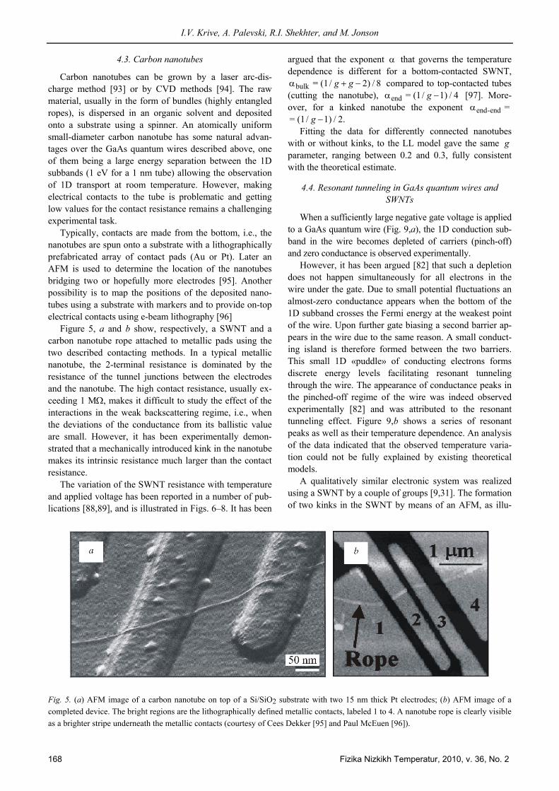
4.3. Carbon nanotubes
Carbon nanotubes can be grown by a laser arc-dis-charge method [93] or by CVD methods [94]. The raw material, usually in the form of bundles (highly entangled ropes), is dispersed in an organic solvent and deposited onto a substrate using a spinner. An atomically uniform small-diameter carbon nanotube has some natural advan-tages over the GaAs quantum wires described above, one of them being a large energy separation between the 1D subbands (1 eV for a 1 nm tube) allowing the observation of 1D transport at room temperature. However, making electrical contacts to the tube is problematic and getting low values for the contact resistance remains a challenging experimental task.
Typically, contacts are made from the bottom, i.e., the nanotubes are spun onto a substrate with a lithographically prefabricated array of contact pads (Au or Pt). Later an AFM is used to determine the location of the nanotubes bridging two or hopefully more electrodes [95]. Another possibility is to map the positions of the deposited nano-tubes using a substrate with markers and to provide on-top electrical contacts using e-beam lithography [96]
Figure 5, a and b show, respectively, a SWNT and a carbon nanotube rope attached to metallic pads using the two described contacting methods. In a typical metallic nanotube, the 2-terminal resistance is dominated by the resistance of the tunnel junctions between the electrodes and the nanotube. The high contact resistance, usually ex-ceeding 1 MΩ, makes it difficult to study the effect of the interactions in the weak backscattering regime, i.e., when the deviations of the conductance from its ballistic value are small. However, it has been experimentally demon-strated that a mechanically introduced kink in the nanotube makes its intrinsic resistance much larger than the contact resistance.
The variation of the SWNT resistance with temperature and applied voltage has been reported in a number of pub-lications [88,89], and is illustrated in Figs. 6–8. It has been
argued that the exponent α that governs the temperature dependence is different for a bottom-contacted SWNT,
bulk = (1/ 2) / 8g gα + − compared to top-contacted tubes (cutting the nanotube), end = (1/ 1) / 4gα − [97]. More-over, for a kinked nanotube the exponent end-end =α= (1/ 1) / 2.g −
Fitting the data for differently connected nanotubes with or without kinks, to the LL model gave the same gparameter, ranging between 0.2 and 0.3, fully consistent with the theoretical estimate.
4.4. Resonant tunneling in GaAs quantum wires and SWNTs
When a sufficiently large negative gate voltage is applied to a GaAs quantum wire (Fig. 9,a), the 1D conduction sub-band in the wire becomes depleted of carriers (pinch-off) and zero conductance is observed experimentally.
However, it has been argued [82] that such a depletion does not happen simultaneously for all electrons in the wire under the gate. Due to small potential fluctuations an almost-zero conductance appears when the bottom of the 1D subband crosses the Fermi energy at the weakest point of the wire. Upon further gate biasing a second barrier ap-pears in the wire due to the same reason. A small conduct-ing island is therefore formed between the two barriers. This small 1D «puddle» of conducting electrons forms discrete energy levels facilitating resonant tunneling through the wire. The appearance of conductance peaks in the pinched-off regime of the wire was indeed observed experimentally [82] and was attributed to the resonant tunneling effect. Figure 9,b shows a series of resonant peaks as well as their temperature dependence. An analysis of the data indicated that the observed temperature varia-tion could not be fully explained by existing theoretical models.
A qualitatively similar electronic system was realized using a SWNT by a couple of groups [9,31]. The formation of two kinks in the SWNT by means of an AFM, as illu-
Fig. 5. (a) AFM image of a carbon nanotube on top of a Si/SiO2 substrate with two 15 nm thick Pt electrodes; (b) AFM image of a completed device. The bright regions are the lithographically defined metallic contacts, labeled 1 to 4. A nanotube rope is clearly visible as a brighter stripe underneath the metallic contacts (courtesy of Cees Dekker [95] and Paul McEuen [96]).

Resonant tunneling of electrons in quantum wires
Fizika Nizkikh Temperatur, 2010, v. 36, No. 2 169
strated in Fig. 10 resulted in a small segment of the nano-tube being limited by two barriers [9].
The observed variation of the conductance peaks versus temperature [9] is shown in Fig. 11. The strong tempe-rature dependence of the peaks was impossible to explain
as a result of sequential or of resonant tunneling, and another theoretical model involving so-called correlated sequential tunneling was invoked to explain the experi-mental data (see Sec. 3.4).
Fig. 6. Conductance G plotted versus temperature T for individual nanotube ropes. (a) Data for ropes that are deposited over pre-definedleads (bulk-contacted); (b) data for ropes that are contacted by evaporating the leads on top of the ropes (end-contacted). The plots showboth the raw data (solid line) and the data corrected for the temperature dependence expected from the Coulomb blockade model(dashed line). The upper inset to (a) shows the power law exponents inferred for a variety of samples. Open circles denote end contactedsamples, and crosses denote bulk-contacted ones (courtesy of Paul McEuen [88]).
1
10
a b
10
110 100T, K
10 100T, K
G,
S�
G,
S�
0 0.2 0.4 0.6 0.8 1.0�
Fig. 7. The differential conductance dI/dV measured at various temperatures. Inset in (a), dI/dV curves taken on a bulk-contacted rope attemperatures T, K: 1.5, 8, 20 and 35. Inset in (b), dI/dV curves taken on an end-contacted rope at temperatures T, K: 20, 40 and 67. In bothinsets, a straight line on the log-log plot is shown as a guide to the eye to indicate power-law behavior (courtesy of Paul McEuen [88]).
a b
T = 8.0 K
T = 35 K
T = 20 K
T = 1.5 K T = 20 K
T = 67 K
T = 40 K
10–1
100
101
10210
0
10–2
10–1
100
101
102
103
eV/kT
V, mV
101
Sca
led
conduct
ance d
I/d
V,
S�
100
101
100
101
102
100
101
V, mV
10–1
100
101
eV/kT
100
Sca
led
conduct
ance d
I/d
V,
S�

I.V. Krive, A. Palevski, R.I. Shekhter, and M. Jonson
170 Fizika Nizkikh Temperatur, 2010, v. 36, No. 2
5. Vibrational effects in resonant electron transport
So far we have considered electron tunneling through a fixed, unmovable quantum dot (QD). However, tunneling of a single electron between nanosized objects is accom-panied by an increase in electrostatic energy which can be comparable to elastic and mechanical energy scales of the system. As a result a significant deformation of the dielectric material which separates the QD from the metallic electrodes can occur if it is mechanically soft. Besides, the tunneling electron can excite vibrational modes of the QD resulting in the appearance of additional (inelastic) channels for electron transport and of polaronic effects. In this section we study the influence of vibrational effects on resonant electron tunneling.
The most evident real systems where all these effects should be pronounced are molecular transistors (see re-views [98,99]). In molecular transistors the role of the central electrode (quantum dot) is played by a single molecule. The interaction of the molecule with the metallic electrodes results, for weak coupling, in a rearrangement and broadening of the molecular energy levels. When the coupling is strong a molecule can provide even perfect transmission through a junction as it was demonstrated in experiments using break-junction devices [100]. In what follows we will assume weak molecule-metal coupling and only consider tunneling transport through molecular junctions. When a molecule bridges a small gap between closely situated metallic electrodes two types of molecular orbitals become significant for electron transport — HOMO (highest occupied molecular orbital) and LUMO (lowest unoccupied molecular orbital) states. For a neutral molecule the Fermi energy of the leads falls into the
LUMO–HOMO energy gap (typically of the order of 1 eV) and the electrical current at low temperatures and bias voltages (V ) is practically blocked unless the gate voltage shifts the LUMO or HOMO states to the «eV-window». Therefore the I–V characteristics of single-molecule transistors can demonstrate resonance features, Coulomb blockade phenomena and conductance oscillations (in large molecules) as a function of gate voltage similar to the analogous effects observed in single-electron transistors formed by laterally confined 2DEGs. The important differences (molecular transistors can function even at room temperatures) are qualitatively explained by the large values of charging energy and level spacing. Although experimental data for molecular junctions strongly vary from molecule to molecule (sometimes by orders of mag-nitude) numerical calculations of their transport properties based on density functional theory are in progress to fit the data (see the recent discussion in Ref. 98).
Fig. 8. Linear-response two-probe conductances G of segments Iand II and across the metal–metal junction of plotted against tem-perature T on a double-logarithmic scale. The data are fitted (sol-id lines) by the power law, ( )G T Tα∼ , which is associated withthe suppression of tunneling density of states in a Luttinger liq-uid. The exponents a for the two straight segments are 0.34 and0.35, respectively. The fit is particularly convincing for the dataacross the kink. An exponent of 2.2 is obtained, which is consis-tent with end-to-end tunneling between two Luttinger liquids(courtesy of Cees Dekker [89]).
Segment ISegment IIAcross the kink
50 100 200 300T, K
10–2
10–1
100
101
G,
S�
Fig. 9. (a) Top view layout of the wire and its contacting scheme. The sample is fabricated using the CEO method. The 1D wire (thick black line) exists along the cleaved surface and overlaps a 2DEG over the entire edge. The metallic gate depletes the 2DEG over a 5 μm wide segment, thereby, forming an isolated 1D wire that is coupled at its ends to the overlapping 2DEG. A further increase in the top gate voltage reduces the wire density conti-nuously to depletion. (b) Conductance of the wire as a function of the top gate voltage. Inset: A zoom-in of the conductance of the wire in the sub-threshold region (courtesy of Ophir Auslaender and Amir Yacoby [82]).

Resonant tunneling of electrons in quantum wires
Fizika Nizkikh Temperatur, 2010, v. 36, No. 2 171
Qualitatively new effects in the transport properties of molecular transistors are associated with vibrational de-grees of freedom of the molecule coupled to the leads. Low-energy vibrational modes result in such new pheno-mena as phonon-assisted electron tunneling [101], polaro-nic effects in electron tunneling (see, e.g., review [99]) and electron shuttling [103].
5.1. Electron transport through a vibrating quantum dot. The model
We now consider the novel effects caused by vibronic modes in electron transport through molecular transistors in the simplest possible theoretical model, which treats the
molecule between the leads as a single-level vibrating quantum dot weakly coupled to leads containing nonin-teracting electrons. This model is too simplified to describe the transport properties of realistic molecular junctions. However, it catches the main features of electron transport in systems with a nanoelectromechanical coupling and would serve as a guide in this novel field of physical research. For a comprehensive review of the field see Ref. 99.
The Hamiltonian of our model (the local Holstein model) is
( ) ( )
= , = ,= ,j j
D tlj L R j L R
H H H H+ +∑ ∑ (36)
where ( ) †= ( )jk j kjl kjkH a aε −μ∑ is the Hamiltonian for
noninteracting electrons with energy kε in the left ( =j L ) and right ( =j R ) leads and jμ is the corresponding chemical potential. The second term,
† † † †0 0= ( ) ,D iH c c b b c c b bε − ε + + ω (37)
is the Hamiltonian of a single-level ( 0ε ) vibrating QD. Here †,c c are standard fermion creation and annihilation operators obeying the canonical commutation relation
†{ , } = 1c c , while †,b b are boson operators and †[ , ] = 1b b ( 0ω is the energy quantum of the boson mode
(vibron)). The second term in Eq. (37) describes a fermion–boson interaction of characteristic strength iε . In our model this interaction originates from the electrostatic coupling of the charge density on the dot to the electrostatic potential produced by the metal electrodes. In what follows we will characterize the strength of the electron–vibron interaction by the dimensionless constant
0= 2 /iλ ε ω . Notice that in our model this coupling constant is a linear function of the driving voltage V (we neglect all nonlinear dependencies induced by polarization effects in a weak electric field /E V d δε , where d
Fig. 10. Fabrication of a room-temperature single-electron transistor within an individual metallic carbon nanotube by manipulationwith an AFM. (a) Nanotube between Au electrodes on top of a Si/SiO2 substrate with a gate-independent resistance of 50 kΩ. (b) Nano-tube after creation of a buckle. The dragging action has resulted in a tube that is bent so strongly that it has buckled. A second draggingaction is performed as indicated by the arrow. (c) Double-buckle nanotube device. (d) Enlarged image of the double-buckle device(courtesy of Cees Dekker [9]).
Fig. 11. Power-law temperature dependence of the conductance,demonstrating correlated sequential tunneling through the nano-tube SET device. Lower data (right-hand scale) show the peakheight Gmax(T) for the conductance, following a power-law func-tion with exponent 0.68. The conductance integrated over thegate voltage range, G*(T) (left-hand scale), also follows a power-law function with exponent 1.66. The inset shows the peak widthw versus T, which displays a linear behavior (courtesy of CeesDekker [9]).
0
0.6
100T, K
w,V
10 1000.1
1
10
100
G,
Sm
ax�
105
104
103
102
10
G*
T, K
� = 1.66
� – 1 = 0.68

I.V. Krive, A. Palevski, R.I. Shekhter, and M. Jonson
172 Fizika Nizkikh Temperatur, 2010, v. 36, No. 2
is the distance between the electrodes and δε is the characteristic level spacing in the molecule),
0
0( ) =
x eVVd
λω
(38)
0 0( = /x Mω is the amplitude of zero-point fluctua-tions of a harmonic oscillator with mass )M . In a general case of inelastic electron tunneling through a molecular junction the strongest coupling between electronic and vibrational degrees of freedom does not have to involve vibrations colinear with the direction of electron tunneling, as was assumed in our model. For a small-amplitude «transverse» vibrational motion we would still have a coupling term in the dot Hamiltonian, Eq. (37), linear in the deviation from the equilibrium position of the dot. However, the corresponding coupling constant would not depend on bias voltage. In what follows we will have in mind an electrostatic coupling model such that shuttle-like transport may dominate the charge transfer through a nano-sized junction. Notice, that in this case the strong coupling regime can be realized (at least theoretically) by applying sufficiently «high» bias voltages. Various aspects of resonant electron transport in the regime of strong electron–vibron interaction is the subject of our considerations in this and the next sections.
The tunneling Hamiltonian ( )jtH in Eq. (36) takes the
form
( ) †ˆ= { ( ) h.c.}.jt j cm kj
kH t X a c +∑ (39)
In the definition Eq. (39) we explicitly took into account the coordinate dependence of the tunneling amplitude
ˆ( cmX is the position operator that corresponds to the cen-ter-of-mass of the dot, †
0ˆ ˆ/ = ( ) / 2cmX x X b b≡ + ).
Since the tunneling probability depends exponentially on the barrier width, it is convenient to model the coordinate dependence of the tunneling amplitude in Eq. (39) by the single-parameter exponential function [103]
0ˆ ˆ( ) = exp( ), = ( , ) = ( , ).j tt X t j X j R Lλ + − (40)
Here 0= /t tx lλ is the dimensionless parameter ( tl is the tunneling length) which along with the coupling constant λ characterizes the electromechanical coupling in our model.
The phenomenon of electron shuttling [103] can be de-scribed, using an «operator language», as the appearance of a time-dependent classical part of the coordinate opera-tor, ˆ = ( )cX x t⟨ ⟩ . It is useful to represent the boson opera-tors in the Hamiltonian, Eq. (37), as a sum of classical and quantum parts (the shift of operators by a c-number is a canonical transformation),
† †ˆ ˆ ˆ ˆ= ( ) , = ( ) , = ( ) ,cb t b b t b X x t x∗α + α + + (41)
where †ˆ ˆˆ( ) = 2Re[ ( )], = ( ) / 2cx t t x b bα + and = 0x⟨ ⟩ by definition. The quantum part of the electron–vibron
interaction in the Hamiltonian, Eq. (37), can be eliminated by a unitary transformation (see, e.g., Ref. 104)
( )† †ˆ ˆˆ ˆ ˆ ˆ= exp( ) , = , = .2iU i pn p b b n c cλ − (42)
This transformation (sometimes called the Lang–Firsov [105] or «small polaron» transformation) is used in a num-ber of theoretical papers dealing with inelastic electron tunneling (see, e.g., the review [99] and references there-in). It allows one to relate the electron–vibron interaction to the tunneling Hamiltonian, which in its turn can be treated perturbatively or by using other approximations.
After unitary transformation the total Hamiltonian takes the form
( ) ( )1 † †
0= , = ,
= = ( ) ,j jp tl
j L R j L RH UHU H t c c b b H− + ε + ω +∑ ∑ (43)
where
20 0( ) = [ ( ) / 2]p ct x tε ε − λ +λ ω (44)
(the term in Eq. (44) proportional to the square of the coupling constant ( 2λ ) is usually called the «polaronic shift»). The transformed tunneling Hamiltonian, Eq. (43), can be expressed as
( ) †0
ˆ= ( h.c.),jt j jkj
kH t a V c +∑ (45)
where 0 0= exp( )j j tt t j− λλ and
ˆˆ = { ( )} , { ( )} = exp{ ( )},j j c j j c t cV T x t Q T x t j x tλ
ˆ ˆ ˆ= exp( ) .j tQ j x i pλ + λ (46)
5.2. Phonon-assisted electron tunneling and polaronic effects
The Hamiltonian described by Eqs. (43), (45), and (46) is the starting point for our theoretical study of vibrational effects in resonant electron tunneling. At first we consider the case when one can neglect the coordinate dependence of the tunneling amplitude ( = 0tλ ). It is physically clear (see the next section) that in this case the equilibrium posi-tion of the quantum dot ( = 0cx ) is stable and there is no electron shuttling phenomenon. Vibrational effects, how-ever, strongly influence the transport properties of molecu-lar junctions and in recent years this problem was theoreti-cally studied in detail (see, e.g., the review [99]).
The most simple and evident effects caused by elect-ron–vibron interactions are: (i) the appearance of inelastic channels for electron transport (phonon-assisted electron tunneling) and (ii) a «polaronic narrowing» (for strong electron–vibron interactions) of the bare width of the dot level. Polaronic effects can also lead to an unusual tem-perature dependence of the conductance.

Resonant tunneling of electrons in quantum wires
Fizika Nizkikh Temperatur, 2010, v. 36, No. 2 173
The electrical current through a vibrating quantum dot coupled to noninteracting electrons in the leads can be cal-culated by using the Meir–Wingreen formula of Eqs. (12), (13), and (14). In our model one can evaluate the average current directly by the equation-of-motion method. The Heisenberg equations of motion for the fermion operators
†( )kj kja a and †( )c c are easy to solve in the so-called «wide band approximation» [101,102] where the density of states in the leads ( = ,j L R ) is assumed to be a constant
jρ (the corresponding partial level widths 2
0 0= 2 | |j j jtΓ πρ are energy independent quantities). When evaluating the averages one needs to know how to decouple the fermion and boson operators. The usual ap-proximation (see, e.g., Ref. 106) is to disregard correla-tions between electrons and vibrons and evaluate boson averages with the Hamiltonian of noninteracting vibrons,
†0=vH b bω , and fermion averages with the fermion part
of the Hamiltonian, Eq. (43) (including the tunneling Ha-miltonian). This decoupling procedure is definitely valid in a perturbation theory where the junction transparency (i.e., the level width 0 0 0= L RΓ Γ +Γ ) is the small parameter, since the electron–vibron interaction enters the Hamilto-nian, Eq. (43), only via the tunneling term. In a number of papers [106–108] (see also Ref. 109 where a self-con-sistent decoupling approximation was suggested) the reso-nant electron tunneling through a vibrating quantum dot was studied in this approach. Although the validity of the decoupling procedure beyond the perturbation region
0 0( , , )T eVΓ ω is not clear, the approach, viewed as a calculational method, allows one to get analytical expres-sions for the whole range of resonant tunneling. Notice that in the limit = 0tλ the boson operator ˆ
jV in Eq. (46) is unitary. The level width, Eq. (11), which in the general case of an x -dependent tunneling amplitude is an operator, coincides with the bare level width 0Γ in the considered limit. This fact allows one to carry out all analytical calcu-lations in the discussed approximation up to the end. In particular, boson averages are reduced to the evaluation of the correlation functions †ˆ ˆ( ) (0)jjQ t Q⟨ ⟩ with the quadratic Hamiltonian of noninteracting vibrons. The quantum dot Green's function in this approach is represented (see, e.g., [106]) as a product of the dot-level Green's function in the single-particle approximation [101,102] and the vibron-induced correlation factor ( )TF t ,
0( ) = ( )exp[ ( / 2) / ] ( ),rv p TG t i t i i t F t− Θ ε + Γ (47)
where the temperature dependent vibron correlation func-tion takes a standard form (see, e.g., Ref. 104)
20
=( ) = exp[ (1 2 )] ( ) exp[ ( / 2 )].T B l
lF t n I z il t i T
∞
−∞−λ + ω +∑
(48)
Here 10= [exp( / ) 1]Bn T −ω − is the Bose–Einstein dis-
tribution function, 22 (1 )B Bz n n≡ λ + , and ( )lI z de-notes the modified Bessel function of the first kind. When evaluating the vibron-induced correlation factor it is as-
sumed that vibrons in the dot are described by the equili-brium distribution function. It means that vibrons are coupled to at heat bath (environment) of temperature T (chosen to be the same as in the leads) and the process of equilibration of their distribution function is rapid
0( /vτ Γ ). This is a plausible assumption in the week-tunneling regime (small ( )L RΓ ) we are dealing with. Non-equilibrated vibrons in a master equation approach were considered in Refs. 110, 111 (see also [112], where the influence of non-equilibrated vibrons on the transport properties of a single-electron transistor was investigated both in the classical and the quantum regime).
The average current through a single-level vibrating quantum dot in the considered approximation takes the form of a sum over inelastic channels of weighted Breit–Wigner contributions [106]
20
=( ) = exp[ (1 2 )] ( )exp( / 2 )B l
l
eJ V n I z l Th
∞
−∞− −λ + − ω ×∑
( )[ ( ) ( )],lBW L Rd T f f
∞
−∞
× ε ε ε − ε∫ (49)
where ( )L Rf are the equilibrium distribution functions of electrons in the leads and
0 02 2
0 0 0( ) = .
( ) ( ) / 4l L RBW
p L RT
lΓ Γ
εε − ε + ω + Γ + Γ
(50)
Positive l-values in Eqs. (49) and (50) correspond to vibron absorption, negative l -values describe processes where l vibron quanta are emitted. This formula was analyzed in Ref. 106 for different regimes of tunnel transport and was questioned in Refs. 112, 113. First of all Eq. (49) in the li-near response limit predicts a suppression of the maximum resonance conductance (which occurs at 0( ) = 0p gVε ) even at = 0T ( 2exp( )G ∝ −λ ). Besides, the low-T linear con-ductance peaks as a function of gate voltage ( gV ) not only on resonance (i.e., at 0( ) = 0p gVε ) but also at the values
( )ngV ( ( )
0( ) = 0,np gV n nε ± ω is an integer) correspond-
ing to the appearance of side-bands. The last claim [106,107] looks very suspicious since at 0T ω and
0eV → only the elastic channel for electron tunneling through the vibrating quantum dot is available. The ques-tionable predictions are artifacts of the approximations (the fermion–boson decoupling procedure and a single-particle approximation for the dot-level Green's function), which were assumed to be valid in low-temperature region
0T Γ . It was shown [112,113] that at low temperatures 0 0( ,T Γ ω ) the maximum (peak) conductance is not
renormalized by vibrational effects and that side-bands do not appear in the gate-voltage dependence of the linear conductance [109,112,114]. Vibrations do influence, even at low temperatures, the shape of the resonance peak by narrowing it. The stronger the electron–vibron interaction, the narrower the «line-shape» [112,114]. This behavior reminds one of resonant tunneling through a symmetric double-barrier in a Luttinger liquid (see Sec. 3.4).

I.V. Krive, A. Palevski, R.I. Shekhter, and M. Jonson
174 Fizika Nizkikh Temperatur, 2010, v. 36, No. 2
The approximations used in the derivation of Eq. (49) (where the decoupling procedure is most sensitive step) is readily justified in the perturbation theory on Γ . Here we consider the temperature behavior of the maximum (peak) conductance at temperatures 0T Γ , when sequential tunneling is the dominating mechanism of electron trans-port through the dot.
For a fixed and rigid (nonfluctuating) QD the resonance conductance scales as 1G T −∝ at 0T Γ (see Sec. 2.2). One can expect that polaronic effects strongly influence electron transport when the tunneling electron is localized for a long time in the dot and therefore can be «dressed» by the vibrational modes. So, it is useful to consider the case when the level width 0Γ is the smallest energy scale in the problem ( 0 0,TΓ ω ). In this limit the spectral function of the dot level is a δ-function and it is easy to get from Eq. (49) the following formula for the maximum conductance [115]
=0 0( ) = ( ) ( / ).G T G T F Tλ λ λ ω (51)
Here =0 ( )G Tλ is the conductance of a single-level quan-tum dot at «high» temperatures (see Eq. (10)) and the scal-ing function ( )F xλ , which has the property that
=0 ( ) = 1F xλ , is represented as a series
2( ) = exp{[ [1 2 ( )]}BF x n xλ −λ + ×
2
2=
exp( / 2) [2 ( )(1 ( ))].
( / 2)coshl B B
l
lx I n x n xlx
∞
−∞
− λ +× ∑ (52)
At low temperatures, 0TΓ ω , one finds that 2( 1) exp( )F xλ −λ . In this region the usual tempera-
ture dependence of the conductance, ( ) /G T Tλ λ∝ Γ , is recovered but with the level width 2= exp( )λΓ Γ −λ re-normalized by zero-point fluctuations of the QD. For strong coupling the renormalized width becomes very nar-row, λΓ Γ , which corresponds to a strongly suppressed probability for electrons to tunnel from bare electronic states in the reservoirs (leads) to polaronic states in the dot. This suppression of linear electron transport is sometimes referred to as a Franck–Condon (or polaronic) blockade [116].
As soon as the temperature becomes of the order of the vibron energy quantum ( 0ω ), thermally excited vibronic modes appear and both the elastic and inelastic channels contribute to the conductance. The contribution of inelastic channels tends to lift the polaronic blockade and the com-petition between elastic and inelastic channels at 0T ≥ ω and 1λ ≥ gives rise to a non-monotonic temperature de-pendence of the conductance [115]. At temperatures in the interval 2
0 0Tω ≤ λ ω (recall that 20λ ω is the pola-
ronic shift and that this quantity defines the polaron energy scale), when the polaronic blockade is already partially lifted, the «high-T» asymptotics of the resonance conduc-tance takes the form [106]
1/2 2
00
0 0( ) exp .
4TG T G
T
−
λ⎛ ⎞⎛ ⎞ λ ωΓ−⎜ ⎟⎜ ⎟ ⎜ ⎟λ ω ω⎝ ⎠ ⎝ ⎠
(53)
At even higher temperatures, 20T λ ω , all polaronic
effects disappear and the conductance scales as / TΓ [115]. The anomalous temperature behavior and 1/ -T scaling of the conductance is a signature of strong polaronic effects in electron transport through a vibrating QD.
The interplay of vibrational and Luttinger liquid effects on electron transport through a vibrating single-level quan-tum dot coupled to Luttinger liquid leads was considered in Ref. 117. There it was shown that in the regime of sequen-tial electron tunneling, for a medium-strong interaction (the corresponding Luttinger liquid correlation parameter
> 1/ 2g ), side-band peaks in the differential conductance dominate over the zero-bias peak (which is suppressed by LL effects).
5.3. Electron shuttling
In previous sections we have discussed the influence of vibrational effects on resonant electron transport while neglecting the coordinate dependence of the electron tunneling amplitude. This is a reasonable approximation for hard potentials or when the strongest coupling between electrons and vibrons are associated with modes unrelated to the direction of electron tunneling. For sufficiently soft potentials (small frequency 0ω in our model) the shift in the position of the dot towards the leads exponentially en-hances the probability of electron tunneling from the near-est electrode. Under certain conditions this results in an instability of the equilibrium position of the QD in the po-tential well between the leads and gives rise to electron shuttling. The phenomenon of electron shuttling was pre-dicted more then 10 years ago [103] and has during the last several years been theoretically investigated for various model systems (see the reviews [11,118,119]) and also observed in experiments [120–122].
A shuttle-like mechanism of electron transfer makes yet another type of resonant electron transport possible, i.e., one where the probability of electron tunneling between the leads is strongly enhanced by the vibrational motion of the quantum dot. In this section we discuss the influence of polaronic effects on electron shuttling — a novel develop-ment of the theory [125]. We derive an equation of motion for the single-electron shuttle in the regime of strong elec-tron–vibron interactions and briefly comment on the influ-ence of polaronic effects on the shuttle instability.
In the process of shuttling the electron is transported from near the source to near the drain electrodes by an os-cillating quantum dot. We model the dot by a harmonic quantum oscillator, Eq. (37). A shuttle instability in this case can be characterized by the appearance of a non-zero expectation value of the coordinate operator ˆ = ( )cX x t⟨ ⟩ , which is possible if the number of vibron excitations is not conserved. In our model, Eq. (36), this is indeed the situa-

Resonant tunneling of electrons in quantum wires
Fizika Nizkikh Temperatur, 2010, v. 36, No. 2 175
tion at hand due to the presence of the electron–vibron interaction and tunneling terms in the Hamiltonian.
In order to consider the shuttle phenomenon we intro-duced the classical (c-number) part ( )tα [ ( )]t∗α of the an-nihilation [creation] operator for vibrons in Eq. (41). This new variable can be interpreted as the amplitude of the vi-bron condensate and its real part describes the instantaneous shift of the oscillator coordinate ( ) = 2Re ( )cx t tα . Now one needs to derive a dynamical equation for this variable (the shuttle equation of motion). For a single-electron shut-tle in the regime of weak electromechanical coupling this classical equation was postulated in Ref. 123 and then re-derived in Ref. 124 by using perturbation theory in the electron tunneling amplitude (weak tunneling).
The Heisenberg equations of motion for the dimensi-onless coordinate ( X ) and momentum ( P ) operators
ˆ ˆ([ , ] =X P i ) can be represented in the form of operator Hamilton equations as
ˆ ˆ ˆ ˆ1 1= , = .ˆ ˆ
dX H dP Hdt dtP X
∂ ∂−
∂ ∂ (54)
In our model, Eq. (43), the Hamiltonian H in Eq. (54) takes the form
( ) ( )2 20ˆ ˆ ˆ ˆ ˆ= ( , ),2
jt
jH X P H X p
ω+ +∑ (55)
where ˆ ˆˆ ˆ= ( ) , = ( )c cX x t x P p t p+ + . The derivative of the tunneling Hamiltonian (defined by Eqs. (45) and (46)) with respect to momentum is proportional to the current opera-tor,
†0
ˆ ˆ= ( h.c.).j j jkjk
iJ t a V c −∑ (56)
It is easy to check the validity of the operator continuity equation ˆ ˆˆ / = L Rdn dt J J+ . With its help one can rewrite Eqs. (54) and (55) in the form of Newton's equation [125]
( )2
202
ˆ ˆ ˆˆ = ,d X n X Fdt
+ λ +ω (57)
where the force operator F is
( ) ( )ˆ
= / , /
ˆ = = ( ) .j jt t tX
j j L RF H j H
− +−∂ λ −∑ ∑ (58)
The nonlinear operator equation defined by Eqs. (57) and (58) is the starting point for our theoretical discussion of a single-electron shuttle in the regime of strong electron–vibron interaction. Since in the shuttle mechanism of elec-tron transport the electron–vibron coupling constant de-pends linearly on the bias voltage, the strong coupling re-gime could be realized at sufficiently «high» voltages.
In order to derive from Eq. (57) the equation of motion for a shuttle (i.e., a closed dynamical equation for the clas-sical coordinate ( )),cx t certain approximations have to be made. We will use (following Ref. 124) perturbation theory in the tunneling amplitude. In this case there are no
problems with the operator character of the level width Γ . In addition the «fermion–boson» decoupling procedure discussed in Sec. 5.2 is justified and all averages can be calculated analytically. The equation for the shuttle coor-dinate can be derived by averaging Eq. (57). It is conve-nient to introduce a new classical variable (transformed coordinate),
1ˆ ˆ( ) = = ( ) , [ ( )] = ,s c cx t UxU x t N N x t n−⟨ ⟩ + λ ⟨ ⟩ (59)
and to derive the equation for this quantity. It takes the form [125]
2
202 ( ) ( ) =s s
d x t x tdt
+ω
2 00
= / , /[ ( )] [ ( )],t
s j sj L R
N x t jH x t− +
λ ω= λω − ∑ (60)
where ( )ˆ= jj tH H⟨ ⟩ . In the limit of weak electromechani-
cal coupling ( 1, 1tλ λ ), when we can omit operator factor ˆ
jQ in the tunneling Hamiltonian, Eq. (45), this equ-ation coincides with the corresponding equation for the classical shuttle [123,124]. Notice that both the average occupation number and the average tunneling Hamiltonian are proportional to the level width 0 0, j jN H∝ Γ ∝ Γ and in perturbation theory one can replace their dependence of
( )cx t with a dependence of ( )sx t in Eq. (60). The shuttle instability in the regime of weak electron–
vibron coupling was considered in Refs. 123, 124, where it was shown that in the absence of mechanical friction the equilibrium time-independent position of QD is unstable at biases 0 0> = 2( )ceV V ε + ω (for resonance tunneling we can let 0 ( ) = 0)gVε and an exponential growth of oscilla-tions occurs 0( ) = exp( )cos( )c ix t x rt tω . At low tempera-tures 0T ω the increment r was found [123,124] to be a linear function of bias voltage 0 tr VΓ λλ ∝∼ . Notice that the increment in this limit is purely classical (it does not depend on ).
In the presence of mechanical friction, which can be taken into account phenomenologically by adding to Eq. (60) a dissipative term proportional to velocity, the incre-ment has to overcome the friction coefficient γ to main-tain electron shuttling. In this case the threshold voltage could be much larger than 0 / eω and we enter the region of strong electron–vibron coupling, 1λ ≥ , where polaronic effects are significant.
How do polaronic effects influence electron shuttling? The shuttle instability is most pronounced at low tempera-tures when at the threshold voltage there is a sharp (step-like) increase of the current signaling the transition to a new regime of electron transport. In the absence of me-chanical friction and when the quantum dot is not pinned by imperfections, the threshold voltage for the resonance condition ( 0 ( ) = 0gVε ) is 02 ω (for a symmetrically bi-ased junction), the coupling to vibrons is weak
0( ) / 1cV x dλ and the polaronic effects are not pro-

I.V. Krive, A. Palevski, R.I. Shekhter, and M. Jonson
176 Fizika Nizkikh Temperatur, 2010, v. 36, No. 2
nounced. They start to influence electron transport at 0 0> ( / )eV d x ω . We showed in the previous section that
at low temperatures strong electron-vibrational mixing results in: (i) a multiplicative renormalization of the effec-tive level width 2
0 0 exp( )Γ → Γ −λ (we consider here the case ( ) tVλ λ ), and (ii) a polaronic shift
20 0 / 2ε → ε −λ . At 0eV ω a large number of inelas-
tic channels contribute to the shuttle instability increment parameter sr . All these effects make the voltage depen-dence of = ( )s sr r V strongly nonlinear.
The interplay between the polaronic (Franck–Condon) blockade, which tends to suppress sr , and the increase in the number of inelastic channels (where each channel en-hances the instability) leads to a non-monotonic behavior of sr as a function of bias voltage with a pronounced max-imum at 2
0 0( / )meV d x ω∼ [125]. Moreover in this re-gion — and at low temperatures 0T ω — the incre-ment ( )sr V oscillates with a period of 0ω and an ampli-tude, which is only a few times smaller the averaged sr [125]. The large «oscillations» of the increment parameter could lead to an unusual behavior of the I–V characteristics for a shuttle-based single-electron transistor. Let us sup-pose that the friction coefficient γ is large enough to damp the shuttle motion at low bias voltages and the shuttle in-stability occurs ( >sr γ ) in the region of large oscillations of the increment. Then a small change of bias voltage (smaller than 0ω ) would transform the system from the shuttle regime of transport (with strongly enhanced tunne-ling probability) to the ordinary regime of tunnel transport (small tunneling probability) and the other way around. In this case one can expect a pronounced negative differential conductance (NDC) in the current–voltage characteristics. The NDC features are spaced by 0ω signaling reentrant transitions to the shuttle regime of electron transport (see also Refs. 111, 116, where NDC in electron transport through a vibrating quantum dot was discussed). Notice that NDC features were observed in the I–V characteristics of suspended carbon nanotubes in the regime of strong electron–vibron coupling [126]. Are these features asso-ciated with a voltage dependence of the electron–vibron coupling or do they have a different origin? This is an open question.
5.4. Electron tunneling through nano-electromechanical systems
The influence of vibrational effects on electron tunne-ling have already been observed in a number of experi-ments: in fullerene-based single-molecular transistors [127,128], in single-molecular metallic junctions [129] including break-junction devices [130], and in suspended quantum dots [131]. In recent years the most promising systems for the study of vibrational effects in electron tunneling spectroscopy appears to be suspended single-wall carbon nanotubes [126,132,133].
In the first experiment on a C60-based molecular tran-sistor [127] characteristic low-energy features in the cur-
rent–voltage characteristics were clearly observed (with the low-energy scale given by 0 5 meVω ). These fea-tures were associated with the quantized motion of the ful-lerene molecule trapped to one of the Au leads by a van der Waals potential. The I–V characteristics measured in Ref. 127 can be explained and fit to theoretical formulas derived both for the shuttle mechanism of electron trans-port [123] and for the purely vibron-assisted tunneling ef-fects [134]. To distinguish between these two different theories, one needs to investigate the current fluctuations (noise). The noise was predicted to be qualitatively differ-ent (as anticipated) for the random vibron-assisted tunne-ling events [107] and for the regular shuttle motion which is synchronized with the electron tunneling [135].
The electron–vibron interaction constant extracted from the experiment by using the theory of Ref. 134 was found to be in the region of medium to strong interaction, 1λ , and (for the best fit) bias- and gate voltage dependent. Al-though the coupling constant obtained from this fit is suffi-ciently strong to reveal polaronic effects, those are not pronounced in the I–V characteristics. In contrast, a differ-ent fit using the shuttle theory achieved a satisfactory agreement between theory and experiment [127] by assum-ing a weak electromechanical coupling [123] where no polaronic effects are expected. Strong polaronic effects (Franck–Condon blockade) were claimed to be observed [126,133] in experiments on suspended carbon nanotubes, where a low-energy quantized phonon mode (the stretching mode of the vibrating nanotube) plays the role of vibron excitations. The electron–vibron coupling constant ( 2λ in our notation) extracted from the experimental data [126] is voltage independent (a physically evident assertion for the nanotube experiments) and does correspond to the regime of strong electron–phonon interactions.
There is one more highly interesting system, namely a carbon nanopeapod, where electromechanical effects could play a significant role in electron transport. A carbon nano-peapod is a hybrid system consisting of a single-wall car-bon nanotube and fullerene molecules encapsulated inside the tube (see, e.g., reviews [136,137]). Carbon peapods were discovered more then 10 years ago [138] and are con-sidered to be a promising system for applications in nano-technology.
Until recently transport experiments on C60-based pea-pods did not show any special features characteristic of nano-electromechanical systems. Furthermore, the trans-port characteristics of empty metallic SWNTs were, as a rule, superior to the analogous quantities measured on car-bon peapods (see, e.g., the review [137] and references therein). This could be explained by technological reasons such as the low quality of peapods used in the early expe-riments. In the process of peapod production the formation of structural defects (for instance, holes on SWNT surface) is dificult to avoid and one can certainly expect strongly defective metallic nanotubes to demonstrate poor conduc-tive properties. Most of the defects are, however, healed when high-quality peapods are produced. For these peapod

Resonant tunneling of electrons in quantum wires
Fizika Nizkikh Temperatur, 2010, v. 36, No. 2 177
systems the influence of the mechanically soft subsystem (encapsulated fullerenes or chains of fullerene molecules) on the conductance properties of metallic SWNT cylinders filled with fullerenes could be unambiguously revealed.
C60 molecules, being electrically neutral objects, cannot directly influence the electrical current flowing along the tube. However, the observation in tunneling experiments [139] of the impact that encapsulated fullerenes have on the electron density of states of a SWNT, suggests a strong hybridization of the conduction electrons with the molecu-lar (LUMO) states of fullerenes. This observation along with the fact that fullerenes and clusters of fullerenes can move easily along the tube axis make carbon nanopeapods promising nano-electromechanical systems. There are claims that electromechanical effects have already been observed in peapods (see, e.g., Ref. 140, where hysteric current–voltage characteristics and the appearance of ran-dom telegraph signal-like current fluctuations are inter-preted as evidence of a shuttle instability in peapods at high bias voltages > 1eV eV). Recently it was also sug-gested [141] that electron backscattering by a vibrating impurity (encapsulated fullerene molecule) could result in a high-temperature excess current. Here we consider the influence of vibrational (polaronic) effects on resonant electron transport through peapod-based quantum dot.
When a peapod bridges the nanogap between the source and drain electrodes the potential barriers at the met-al/SWNT contacts allow one to treat the nanotube as a multilevel quantum dot coupled to the vibrating fullerenes. In the simplest theoretical model we will consider a single side-impurity which represents a 60C molecule (or a clus-ter of fullerenes) confined in a small region inside the tube. The evident transverse confinement results in an energy scale for the transverse vibrational excitations of the order of 10 meV (see, e.g., [142]) for small-diameter peapods ( 1.3d ≥ nm) usually exploited in experiments. The longi-tudinal confinement, produced for instance by two closely situated holes on the nanotube surface (hole repels encap-sulated molecule), could result in far smaller value (by orders of magnitude) of vibrational energy quantum. Since we are interested in low-temperature transport properties we will consider only longitudinal vibrations.
The shift xδ in the position of the scatterer (fullerene) along the tube disturbs all quantized electron energy levels in a metallic SWNT by = ( / )n F nv k x xδε ∂ ∂ δ ( nk is the electron momentum). The Hamiltonian of the quantum dot in this model takes the form [115]
† † † †0 0= ( , )( ) ,QD n n n n n n
n nH c c L l b b c c b bε + ω λ + + ω∑ ∑
(61)
where ( , )n L lλ is the energy- and position-dependent elec-tron–vibron coupling constant ( L is the peapod length, l is the equilibrium position of the scatterer inside the tube). It was shown [115] that 2
nλ strongly fluctuates from level
to level even in the case when the actual level spacings are close to the mean level spacing ( = /L Fv LΔ π ).
It is easy to apply the theory of electron transport through a vibrating quantum dot (see Sec. 5.2) to the con-sidered model. Since the electron–vibron coupling constant strongly differs for different levels n, some levels strongly couple to the vibrations and the resonant conductance through these levels is influenced by polaronic effects (po-laronic narrowing of level width, anomalous temperature behavior). Other levels are decoupled from the vibrational modes and electron tunneling through these levels are de-scribed by the usual Breit–Wigner theory. As was already discussed in Sec. 5.2 the developed theory is valid at tem-peratures nT Γ . It means that to compare theory and experiment on resonant electron tunneling through peapods [143,144], one has to select only very narrow peaks (in a plot of conductance versus gate voltage) broadened by temperature effects. In the experiment Ref. 144 the regime of strong coupling between the dot and the leads was rea-lized (since signatures of Kondo physics were reported) and the theory developed in Ref. 115 cannot be applied to fit the experimental data. A selective choice of peaks in the experiment Ref. 143 and new measurements with weakly coupled tunneling junctions show evidence of vibrational effects in resonant electron transport through peapod-based molecular transistors [145].
6. Conclusion
Resonant tunneling of electrons is a quantum coherent phenomenon, which allows one to probe elementary exci-tations in condensed matter systems with high precision. While the positions of resonant conductance peaks contain information about the energy spectrum, the transmission intensity provides direct information about the wave func-tions of the charge carriers in the conductor under investi-gation (the tunneling matrix elements are determined by the overlap of the wave function of the tunneling electron and the wave function of charge excitations in the region through which the electron tunnels). Both quantities are strongly affected by the electron–electron interaction and by the interaction of electrons with other degrees of free-dom. These interaction effects result in the appearance of new and different energy scales, which determine specific features of the resonant electron transport characteristics. Therefore, it is reasonable to regard electron tunneling in resonant structures as a transducer that could convert one form of energy (e.g., mechanical) to another. In this Re-view we have already discussed the coupling of electrons to nanomechanical (radio frequency) vibrations when studying electron shuttling (see Sec. 5.3).
It is interesting to consider here other opportunities. The coupling of coherent electrons to an external high-frequency electromagnetic field has been shown to result in a number of interesting nonequilibrium phenomena (both in normal [146,147] and in superconducting [148,149] mesoscopic structures) if the microwave photon

I.V. Krive, A. Palevski, R.I. Shekhter, and M. Jonson
178 Fizika Nizkikh Temperatur, 2010, v. 36, No. 2
energy is comparable to the electronic energy-level spac-ing. The mechanical frequencies of nanoelectromechanical devices, on the other hand, can easily be tuned to match the low-energy scales of tunnel structures such as the level width, the applied bias voltage, or the frequency of Rabi oscillations in the populations of energy levels. These two very different scales of energy both have a bearing on re-sonant electron transport and one may speculate that cohe-rent electrons in single-electron tunneling (SET) transistors can be used as microwave-mechanical transducers by si-multaneously coupling them to both an electromagnetic and to nanomechanical degrees of freedom.
Acknowledgments
This work was supported in parts by the Swedish VR and SSF, by the Faculty of Science at the University of Go-thenburg through the «Nanoparticle» Research Platform, and by the Korean WCU programme funded by MEST through KOSEF (R31-2008-000-10057-0). IVK gratefully acknowledges financial support from a joint grant from the Ministries of Education and Science in Israel and Ukraine and from the grant «Effects of electronic, magnetic and elastic properties in strongly inhomogeneous nanostruc-tures» provided by the National Academy of Sciences of Ukraine. IVK thanks the Department of Physics at the Uni-versity of Gothenburg and the School of Physics and As-tronomy at Tel Aviv University for hospitality.
1. G. Gamow, Nature 122, 805 (1928). 2. R.H. Fowler and L.W. Nordheim, Proc. Royal Soc. (London)
A119, 173 (1928). 3. J.W. Gadzuk and E.W. Plummer, Rev. Mod. Phys. 45, 487
(1973). 4. G. Breit and E. Wigner, Phys. Rev. 49, 519 (1936). 5. L.D. Landau and E.M. Lifshits, Quantum Mechanics (Non-
Relativistic Theory), Pergamon Press, Oxford (1977). 6. J. Nygard, D.H. Cobden, M. Bockrath, P.L. McEuen, and
P.E. Lindelof, Appl. Phys. A69, 297 (1999). 7. R. Egger, A. Bachtold, M. Fuhrer, M. Bockrath, D. Cobden,
and P. McEuen, Luttinger Liquid Behavior in Metallic Car-bon Nanotubes, in: Interacting Elektrons in Nanostructures, R. Haug and H. Schoeller (eds.), Springer (2000); cond-mat/0008008, 1 August (2000).
8. C.L. Kane and M.P.A. Fisher, Phys. Rev. B46, 15233 (1992). 9. H.W.Ch. Postma, T. Teepen, Z. Yao, M. Grifoni, and C.
Dekker, Science 293, 76 (2001). 10. Yu.G. Naidyuk and I.K. Yanson, Point-Contact Spectrosco-
py, Springer Series in Solid State Sciences, vol. 145, Springer Science and Business Media Inc. (2005).
11. R.I. Shekhter, Yu. Galperin, L.Y. Gorelik, A. Isacsson, and M. Jonson, J. Phys.: Condens. Matter 15, R441 (2003).
12. R. Landauer, IBM J. Res. Develop. 1, 223 (1957); Philos. Mag. 21, 863 (1970).
13. D.K. Ferry and S.M. Goodnick, Transport in Nanostructures, Cambridge Univ. Press, Cambridge (1997).
14. H. van Houten and C. Beenakker, Physics Today 49, 22 (1996).
15. J. Koch, F. von Oppen, and A.V. Andreev, Phys. Rev. B74, 205438 (2006).
16. M. Büttiker, Phys. Rev. B33, 3020 (1986); IBM J. Res. De-velop. 32, 63 (1988).
17. F.D.M. Haldane, Phys. Rev. Lett. 67, 937 (1991). 18. I.V. Krive and E.R. Mucciolo, Phys. Rev. B60, 1429 (1999). 19. T. Weil and B. Vinter, Appl. Phys. Lett. 50, 1281 (1987). 20. M. Jonson and A. Grincwajg, Appl. Phys. Lett. 51, 1729
(1987). 21. Y. Zohta, Jpn. J. Appl. Phys. 32, L177 (1993). 22. C.W.J. Beenakker, Phys. Rev. B44, 1646 (1991). 23. Single Charge Tunneling: Coulomb Blockade Phenomena in
Nanostructures, H. Grabert and M.H. Devoret (eds.), Plenum, New York (1992).
24. R.I. Shekhter, Zh. Eksp. Teor. Fiz. 63, 1410 (1972) [Sov. Phys. JETP 36, 747 (1972)]; I.O. Kulik and R.I. Shekhter, Zh. Eksp. Teor. Fiz. 68, 623 (1975) [Sov. Phys. JETP 41, 308 (1975)].
25. S. Datta, Electronic Transport in Mesoscopic Systems, Cam-bridge Univ. Press, Cambridge (1995).
26. F. Duan and J. Guojun, Introduction to Condensed Matter Physics, Vol. 1, World Scientific Publishing Co. (1995).
27. L.I. Glazman and M.E. Raikh, Pisma Zh. Eksp. Teor. Fiz. 47, 378 (1988) [JETP Lett. 47, 452 (1988)]; T.K. Ng and P.A. Lee, Phys. Rev. Lett. 61, 1768 (1988).
28. H. Houng and A.-P. Jauho, Quantum Kinetics in Transport and Optics of Semiconductors, Springer-Verlag, Berlin (1996).
29. Y. Meir and N.S. Wingreen, Phys. Rev. Lett. 68, 2512 (1992). 30. A.-P. Jauho, N.S. Wingreen, and Y. Meir, Phys. Rev. B50,
5528 (1994). 31. D. Bozovic, M. Bockrath, J.H. Hafner, C.M. Lieber, H. Park,
and M. Tinkham Appl. Phys. Lett. 78, 3693 (2001). 32. Zh. Yao, C. Dekker and Ph. Avouris, Electron Transport
Trough Single-Wall Carbon Nanotubes, in: Carbon Nano-tubes: Synthesis, Structure, Properties and Applications, M.S. Dresselhaus, G. Dresselhaus, and Ph. Avouris (eds.), Springer (2001).
33. A.O. Gogolin, A.A. Nersesyan, and A.M. Tsvelik, Bosoniza-tion and Strongly Correlated Systems, Cambridge University Press (1998).
34. K. Schönhammer, Luttinger Liquids: The Basic Concepts, in: Interacting Electrons in Low Dimensions, D. Baeriswyl (ed.), Dordrecht: Kluwer Academic Publishers (2005).
35. A. Furusaki, Phys. Rev. B57, 7141 (1998). 36. L.I. Glazman and R.I. Shekhter, J. Phys.: Condens. Matter 1,
5811 (1989). 37. A. Braggio, M. Sassetti, and B. Kramer, Phys. Rev. Lett. 87,
146802 (2001). 38. A. Braggio, M. Grifoni, M. Sassetti, and F. Napoli, Europhys.
Lett. 50, 236 (2000). 39. J.U. Kim, I.V. Krive, and J.M. Kinaret, Phys. Rev. Lett. 90,
176401 (2003). 40. F. Cavaliere, A. Braggio, J.T. Stockburger, M. Sassetti, and
B. Kramer, Phys. Rev. Lett. 93, 036803 (2004). 41. J.U. Kim, J.M. Kinaret, and M.S. Choi, J. Phys.: Condens.
Matter 17, 3815 (2005).

Resonant tunneling of electrons in quantum wires
Fizika Nizkikh Temperatur, 2010, v. 36, No. 2 179
42. J.U. Kim, M.S. Choi, I.V. Krive, and J.M. Kinaret, Fiz. Nizk. Temp. 32, 1522 (2006) [Low Temp. Phys. 32, 1158 (2006)].
43. A. Furusaki and N. Nagaosa, Phys. Rev. B47, 3827 (1993). 44. K.A. Matveev, D. Yue, and L.I. Glazman, Phys. Rev. Lett. 71,
3351 (1993); D. Yue, K.A. Matveev, and L.I. Glazman, Phys. Rev. B49, 1966 (1994).
45. L.I. Glazman, I.M. Ruzin, and B.I. Shklovskii, Phys. Rev. B45, 8454 (1992).
46. A. Komnik and A.O. Gogolin, Phys. Rev. Lett. 90, 246403 (2003).
47. K.A. Matveev, Phys. Rev. B51, 1743 (1995). 48. Yu.V. Nazarov and L.I. Glazman, Phys. Rev. Lett. 91, 126804
(2003). 49. M. Fabrizio and A.O. Gogolin, Phys. Rev. B51, 17827 (1995). 50. M. Thorwart, M. Grifoni, G. Cuniberti, H.W.Ch. Postma, and
C. Dekker, Phys. Rev. Lett. 89, 196402 (2002); M. Thorwart, R. Egger, and M. Grifoni, Phys. Rev. B72, 035330 (2005).
51. S. Hügle and R. Egger, Europhys. Lett. 66, 565 (2004). 52. V. Meden, T. Enss, S. Andergassen, W. Metzner, and K.
Schönhammer, Phys. Rev. B71, 041302(R) (2005); V. Me-den, S. Andergassen, X. Barnabé-Thériault, W. Metzner, and K. Schönhammer, Phys. Rev. B71, 155401 (2005).
53. D. Loss, Phys. Rev. Lett. 69, 343 (1992). 54. A.O. Gogolin and N.V. Prokof'ev, Phys. Rev. B50, 4921
(1994). 55. I.V. Krive, P. Sandström, R.I. Shekhter, S.M. Girvin, and M.
Jonson, Phys. Rev. B52, 16451 (1995). 56. C.M. Canali, W. Stefan, L.Y. Gorelik, R.I. Shekhter, and M.
Jonson, Europhys. Lett. 40, 67 (1997). 57. P. Sandström and I.V. Krive, Ann. Phys. (NY) 257, 18
(1997); I.V. Krive, P. Sandström, R.I. Shekhter, and M. Jon-son, Europhys. Lett. 38, 213 (1997).
58. M. Pletyukhov and V. Gritsev, Phys. Rev. B70, 165316 (2004).
59. A.A. Zvyagin and I.V. Krive, Fiz. Nizk. Temp. 21, 687 (1995) [Low Temp. Phys. 21, 533 (1995)].
60. I.O. Kulik, Pis'ma Zh. Eksp. Teor. Fiz. 11, 407 (1970) [JETP Lett. 11, 275 (1970)].
61. M. Büttiker, Y. Imry, and R. Landauer, Phys. Lett. A96, 365 (1983).
62. H.-F. Cheung, Y. Gefen, E.K. Riedel, and W.-H. Shih, Phys. Rev. B37, 6050 (1988).
63. P. Sandström and I.V. Krive, Phys. Rev. B56, 9255 (1997). 64. A. Müller-Groeling, H.A. Weidenmüller, and C.H. Lewen-
kopf, Europhys. Lett. 22, 193 (1993). 65. L.Y. Gorelik, I.V. Krive, S.I. Kulinich, R.I. Shekhter, and M.
Jonson, Europhys. Lett. 57, 409 (2002). 66. A. Nogaret, J.-C. Portal, H.E. Beere, D.A. Ritchie, and C.
Phillips, Fiz. Nizk. Temp. 34, 1081 (2008) [Low Temp. Phys. 34, 853 (2008)].
67. A. Nogaret, J.-C. Portal, H.E. Beere, D.A. Ritchie, and C. Phillips, J. Phys.: Condens. Matter 21, 025303 (2009).
68. X.G. Wen, Phys. Rev. B41, 12838 (1990). 69. A.M. Chang, Rev. Mod. Phys. 75, 1449 (2003). 70. I.V. Krive, S.I. Kulinich, L.Y. Gorelik, R.I. Shekhter, and M.
Jonson, Phys. Rev. B64, 045114 (2001).
71. H. Bateman and A. Erdelyi, Higher Transcendental Func-tions, Vol.1, McGraw-Hill, New York (1953).
72. R. Egger and H. Grabert, Phys. Rev. Lett. 75, 3505 (1995). 73. D.E. Feldman and Y. Gefen, Phys. Rev. B67, 115337 (2003). 74. B.J. van Wees, H. van Houten, C.W.J. Beenakker, J.G. Wil-
liamson, L.P. Kouwenhoven, D. van der Marel, and C.T. Foxon, Phys. Rev. Lett. 60, 848 (1988).
75. D.A. Wharam, T.J. Thornton, R. Newbury, M. Pepper, H. Ahmed, J.E.F. Frost, D.G. Hasko, D.C. Peacock, D.A. Rit-chie, and G.A.C. Jones, J. Phys. C21, L209 (1988).
76. C. Tarucha, T. Honda, and T. Saku, Solid State Commun. 94, 413 (1995).
77. E. Kapon, D.M. Hwang, and R. Bhat, Phys. Rev. Lett. 63, 430 (1989).
78. L.N. Pfeiffer, H.L. Stormer, K.W. Baldwin, K.W. West, A.R. Goni, A. Pinczuk, R.C. Ashoori, M.M. Dignam, and W. Wegscheider, J. Crys. Growth 127, 849 (1993).
79. A. Yacoby, H.L. Stormer, N.S. Wingreen, K.W. Baldwin, L.N. Pfeiffer, and K.W. West, Phys. Rev. Lett. 77, 4612 (1996).
80. D. Kaufman, Y. Berk, B. Dwir, A. Rudra, A. Palevski, E. Ka-pon, and W.A. de Heer, Phys. Rev. B59, R10433 (1999).
81. E. Levy, A. Tsukernik, M. Karpovski, A. Palevski, B. Dwir, E. Pelucchi, A. Rudra, E. Kapon, and Y. Oreg, Phys. Rev. Lett. 97, 196802 (2006).
82. O. Auslaender, A. Yacoby, R. de Picciotto, K.W. Baldwin, L.N. Pfeiffer, and K.W. West, Phys. Rev. Lett. 84, 1764 (2000).
83. T. Ando, Semicond. Sci. Technol. 15, R13 (2000). 84. W. Liang, M. Bockrath, and H. Park, Phys. Rev. Lett. 88,
126801 (2002). 85. S. Frank, P. Poncharal, Z.L. Wang, and W.A. de Heer,
Science 280, 1744 (1998). 86. R.D. Antonov and A.T. Johnson, Phys. Rev. Lett. 83, 3274
(1999). 87. J. Appenzeller, J. Knoch, M. Radosavljevic, and Ph. Avouris,
Phys. Rev. Lett. 92, 226802 (2004). 88. M. Bockrath, D.H. Cobden, J. Lu, A.G. Rinzler, R.E. Smal-
ley, L. Balents, and P.L. McEuen, Nature 397, 598 (1999). 89. Z. Yao, H.W.Ch. Postma, L. Balents, and C. Dekker, Nature
402, 273 (1999). 90. B. Dwir, D. Kaufman, E. Kapon, and A. Palevski, Europhys.
Lett. 55, 80 (2001). 91. D.L. Maslov, Phys. Rev. B52, R14368 (1995). 92. Y. Oreg and A.M. Finkel'stein, Phys. Rev. B54, R14265
(1996). 93. A. Thess, R. Lee, P. Nikolaev, H. Dai, P. Petit, J. Robert, C.H.
Xu, Y.H. Lee, S.G. Kim, A.G. Rinzler, D.T. Colbert, G.E. Scuseria, D. Tomanek, J.E. Fischer, and R.E. Smalley, Science 273, 483 (1996).
94. J.H. Hafner, M.J. Bronikowski, B.R. Azamian, P. Nikolaev, A.G. Rinzler, D.T. Colbert, K.A. Smith, and R.E. Smalley, Chem. Phys. Lett. 296, 195 (1998).
95. S.J. Tans, M.H. Devoret, H. Dai, A. Thess, R.E. Smalley, L.J. Geeligs, and C. Dekker, Nature 386, 474 (1997).
96. M. Bockrath, D.H. Cobden, P.L. McEuen, N.G. Chopra, A. Zettl, A. Thess, and R.E. Smalley, Science 275, 1922 (1997).

I.V. Krive, A. Palevski, R.I. Shekhter, and M. Jonson
180 Fizika Nizkikh Temperatur, 2010, v. 36, No. 2
97. R. Egger and A.O. Gogolin, Phys. Rev. Lett. 79, 5082 (1997). 98. S.M. Lindsay and M.A. Ratner, Adv. Mater. 19, 23 (2007). 99. M. Galperin, M.A. Ratner, and A. Nitzan, J. Phys.: Cond.
Matter 19, 103201 (2007). 100. R.H.M. Smit, Y. Noat, C. Untiedt, N.D. Lang, M. van He-
mert, J.M. van Ruitenbeek, Nature 419, 906 (2002). 101. L.I. Glazman and R.I. Shekhter, Zh. Eksp. Teor. Fiz. 94, 292
(1988) [Sov. Phys. JETP 67, 163 (1988)]. 102. N.S. Wingreen, K.W. Jacobsen, and J.W. Wilkins, Phys. Rev.
B40, 11834 (1989). 103. L.Y. Gorelik, A. Isacsson, M.V. Voinova, B. Kasemo, R.I.
Shekhter, and M. Jonson, Phys. Rev. Lett. 80, 4526 (1998). 104. G. Mahan, Many-Particle Physics, 2nd edition, Plenum Press,
NY (1990). 105. I.G. Lang and Y.A. Firsov, Sov. Phys. JETP 16, 1301 (1963). 106. U. Lundin and R.H. McKenzie, Phys. Rev. B66, 075303
(2002). 107. J.-X. Zhu and A.V. Balatsky, Phys. Rev. B67, 165326 (2003). 108. A.S. Alexandrov, A.M. Bratkovsky, and R.S. Williams, Phys.
Rev. B67, 075301 (2003). 109. M. Galperin, A. Nitzan, and M.A. Ratner, Phys. Rev. B73,
045314 (2006). 110. D. Boese and H. Schoeller, Europhys. Lett. 54, 668 (2001). 111. K.D. McCarthy, N. Prokof'ev, and M.T. Tuominen, Phys.
Rev. B67, 245415 (2003). 112. A. Mitra, I. Aleiner, and A.J. Millis, Phys. Rev. B69, 245302
(2004). 113. R. Egger and A.O. Gogolin, Phys. Rev. B77, 113405 (2008). 114. K. Flensberg, Phys. Rev. B68, 205323 (2003). 115. I.V. Krive, R. Ferone, R.I. Shekhter, M. Jonson, P. Utko, and
J. Nygård, New J. Phys. 10, 043043 (2008). 116. J. Koch and F. von Oppel, Phys. Rev. Lett. 94, 206804 (2005);
J. Koch, F. von Oppel, and A.V. Andreev, Phys. Rev. B74, 205438 (2006).
117. G.A. Skorobagat'ko and I.V. Krive, Fiz. Nizk. Temp. 34, 1086 (2008) [Low Temp. Phys. 34, 858 (2008)].
118. R.I. Shekhter, R.I. Gorelik, M. Jonson, Y.M. Garpelin, and V.M. Vinokur, J. Comput. Theor. Nanosci. 4, 860 (2007).
119. R.I. Shekhter, F. Santandrea, G. Sonne, L.Y. Gorelik, and M. Jonson, Fiz. Nizk. Temp. 35, 841 (2009) [Low Temp. Phys. 35, 662 (2009)].
120. M.T. Tuominen, R.V. Krotkov, and M.L. Breuer, Phys. Rev. Lett. 83, 3025 (1999).
121. Y. Majima, K. Nagano, and A. Okuda, Jpn J. Appl. Phys. 41, 5381 (2002); K. Nagano, A. Okuda, and Y. Majima, Appl. Phys. Lett. 81, 544 (2002).
122. A.V. Moskalenko, S.N. Gordeev, O.F. Koentjoro, P.R. Raith-by, R.W. French, F. Marken, and S.E. Savel'ev, Giving Elec-trons a Ride: Nanomechanical Electron Shuttles, cond.-mat. 0810.2430v1 (2008).
123. D. Fedorets, L.Y. Gorelik, R.I. Shekhter, and M. Jonson, Eu-rophys. Lett. 58, 99 (2002).
124. D. Fedorets, Phys. Rev. B68, 033106 (2003). 125. G.A. Skorobagat'ko, I.V. Krive, and R.I. Shekhter, Fiz. Nizk.
Temp. 35, 1221 (2009) [Low Temp. Phys. 35, No. 12 (2009)]. 126. S. Sampaz, P. Jarillo-Herrero, Ya.M. Blanter, C. Dekker, and
H.S.J. van der Zant, Phys. Rev. Lett. 96, 026801 (2006).
127. H. Park, J. Park, A.K.L. Lim, E.H. Anderson, A.P. Alivisatos, and P.L. McEuen, Nature 407, 57 (2000).
128. A.N. Pasupathy, J. Park, C. Chang, A.V. Soldatov, S. Lebed-kin, R.C. Bialczak, J.E. Grose, L.A.K. Donev, J.P. Sethna, D.C. Ralph, and P.L. McEuen, Nano Lett. 5, 203 (2005).
129. L.H. Yu, Z.K. Keane, J.W. Ciszek, L. Cheng, M.P. Stewart, J.M. Tour, and D. Natelson, Phys. Rev. Lett. 93, 266802 (2004).
130. R.H. M. Smit, Y. Noat, C. Untiedt, N.D. Lang, M. van He-mert, J.M. van Ruitenbeek, Nature 419, 906 (2002).
131. E.M. Weig, R.H. Blick, T. Brandes, J. Kirschbaum, W. Weg-scheider, M. Bichler, and J.P. Kotthaus, Phys. Rev. Lett. 92, 046804 (2004).
132. A.K. Hüttel, M. Poot, B. Witkamp, and H.S.J. van der Zant, New J. Phys. 10, 095003 (2008).
133. R. Leturcq, C. Stampfer, K. Inderbitzin, L. Durrer, C. Hierold, E. Mariani, M.G. Schultz, F. von Oppen, and K. Ensslin, Na-ture Physics 5, 327 (2009).
134. S. Braig and K. Flensberg, Phys. Rev. B68, 205324 (2003). 135. F. Pistolesi, Phys. Rev. B69, 245409 (2004). 136. M. Monthioux, Carbon 40, 1809 (2002). 137. I.V. Krive, R.I. Shekhter, and M. Jonson, Fiz. Nizk. Temp. 32,
1171 (2006) [Low Temp. Phys. 32, 887 (2006)]. 138. B.W. Smoth, M. Monthioux, and D.E. Luzzi, Nature 396,
323 (1998). 139. D.J. Hornbaker, S.-J. Kahng, S. Misra, B.W. Smith, A.T.
Johnson, E.J. Mele, D.E. Luzzi, and A. Yazdani, Science 295, 828 (2002).
140. H.Y. Yu, Dong Su Lee, Ursula Dettlaff-Weglikowska, Sieg-mar Roth, and Yung Woo Park, Phys. Rev. B78, 155415 (2008).
141. G. Sonne, L.Y. Gorelik, R.I. Shekhter, and M. Jonson, Euro-phys. Lett. 84, 27002 (2008).
142. L.A. Girifalco, M. Hodak, and R.S. Lee, Phys. Rev. B62, 13104 (2000).
143. P. Utko, J. Nygard, M. Monthioux, and L. Noe, Appl. Phys. Lett. 89, 233118 (2006).
144. C.H.L. Quay, J. Cumings, S.J. Gamble, A. Yazdani, H. Ka-taura, and D. Goldhaber-Gordon, Phys. Rev. B76, 073404 (2007).
145. P. Utko et al. (in preparation). 146. A. Grincwajg, L.Y. Gorelik, V.Z. Kleiner, and R.I.
Shekhter, Phys. Rev. B52, 12168 (1955). 147. L.Y. Gorelik, Frank A. Maaø, R.I. Shekhter, and M. Jonson,
Phys. Rev. Lett. 78, 3169 (1997). 148. L.Y. Gorelik, V.S. Shumeiko, R.I. Shekhter, G. Wendin, and
M. Jonson, Phys. Rev. Lett. 75, 1162 (1995). 149. L.Y. Gorelik, N.I. Lundin, V.S. Shumeiko, R.I. Shekhter, and
M. Jonson, Phys. Rev. Lett. 81, 2538 (1998).