r&d and commercialization of improved epi droop · • require high luminance leds for...
TRANSCRIPT
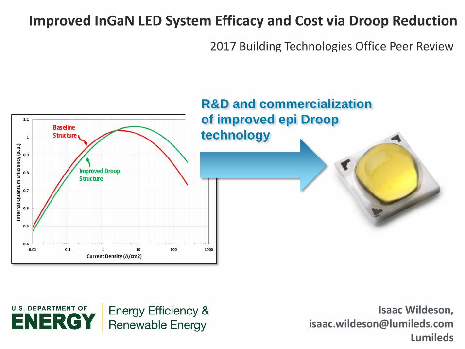
Improved DroopStructure
BaselineStructure
Isaac Wildeson, [email protected]
Lumileds
Improved InGaN LED System Efficacy and Cost via Droop Reduction
2017 Building Technologies Office Peer Review
R&D and commercialization of improved epi Droop technology

2
Project SummaryTimeline:Start date: September 1, 2015Planned end date: August 31, 2017Key Milestones1. Compare defects within moderate and aggressive LED
designs for Droop improvement and determine if categorically new defects emerge; November 30, 2016
2. Demonstrate controllable defect mitigation through optimized growth/design conditions for low Droop structures; February 24, 2017
3. Year 1 EQE gain target over baseline @ 100A/cm2,Tj=85°C; September 26, 2016
4. Year 2 EQE gain target over baseline @ 100A/cm2, Tj=85°C; August 31, 2017
Budget:Total Project $ to Date: • DOE: $807,891• Cost Share: $240,501
Total Project $:• DOE: $1,255,990• Cost Share: $374,000
(excluding National Lab budgets)
Key Partners:
Project Outcome: Improve high current efficiency in InGaN LEDs to reduce energy consumption of directional light sources and enable flexibility in LED system design driving LED adoption in a broader array of lighting applications
Brookhaven National Laboratory
Massachusetts Institute of Technology
Sandia National Laboratories

3
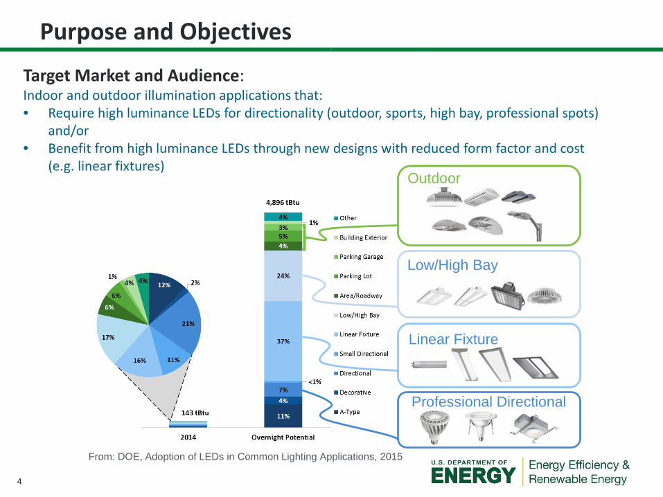
Purpose and Objectives
Problem Statement:
• Reaching the DOE SSL MYPP target of >75% EQE at 100A/cm2, 85C requires significant improvement in efficiency droop – the reduction in efficiency with increased drive current
• Improved high current efficiency and reduction in total system cost are required for increased large-scale adoption of SSL
• This DOE-assisted project is focused on improving LED high current efficiency by using advanced material characterization techniques to understand defects that form in low Droop structures, and inform the epitaxial growth process development
Light output per dollar (LOP/$) can benefit significantly if we can mitigate Droop
High drive current Low drive current
Baseline status
Improved DroopStructure
Improved DroopStructure with material quality degradation
Baseline Structure
Simulated impact of material quality degradation on low Droop structures
“Droop” is the rollover in efficiency at high current
4
Purpose and Objectives
Outdoor
Low/High Bay
Linear Fixture
Professional Directional
From: DOE, Adoption of LEDs in Common Lighting Applications, 2015
Target Market and Audience: Indoor and outdoor illumination applications that:• Require high luminance LEDs for directionality (outdoor, sports, high bay, professional spots)
and/or• Benefit from high luminance LEDs through new designs with reduced form factor and cost
(e.g. linear fixtures)

5
Purpose and Objectives
Impact of Project: Commercialization of two epi generations with significant high current efficiency gains (one at end of each Year 1 and Year 2)Technical understanding on the defect mechanisms that form in low Droop structures and how epitaxial growth can be altered to mitigate these to guide future low Droop epi development The achievements of this project are measured by:
a. Near-term: EQE improvements at 100A/cm2, understanding of defect mechanisms in low Droop structures, commercialization of epi improvements
b. Intermediate-term: utilization of technical understanding for development and commercialization of future high current efficiency improvements, system level design freedom realized with small high luminance sources
c. Long-term: utilization of LEDs with high efficiency at high currents in extended applications that take advantage of efficient small source sizes for significant system level cost reductions

6
Approach
Approach: • Predictive device modeling guides low Droop LED active region designs• MOCVD growth development focused on producing the desired active region designs
while trying to maintain high material quality• Complimentary advanced material characterization techniques (DLOS, TEM/STEM, etc.)
and LED characterization data (PL, lamp EL/EQE, etc.) guide one another and feed back to understand the source of specific defects impacting IQE, and how they are affected by the epitaxial growth conditions
Key Issues: Progress has been made in identifying which defect types are impacting IQE in low Droop structures, but further work is required for determining specific microscopic identities of defects. Continued work focused on correlating controlled MOCVD growth changes with advanced characterization feedback is ongoing to better identify specific microscopic defects.
7
Approach
Distinctive Characteristics: • Project focuses on solving relevant issues in state-of-the-art industry devices• Combines advanced characterization techniques and expertise from Academia
and National Laboratories (typically not present in-house in industry) with industry MOCVD epitaxial growth expertise
• Quick time-to-market commercialization of the developed improvements– Commercialization of Year 1 improvements hitting the market prior to
project completion

8
Progress and Accomplishments
• Certain MOCVD processes evaluated for growth of some candidate low-Droop designs show local fluctuations in quantum well width (WWFs)– Can be intentionally exaggerated by changes in MOCVD processes within test structure
LEDs (as in example cross-section micrograph below) to check correlation with EQE– Device EQE may have some correlation with WWFs, but they are not the dominant
factor of SRH recombination in low Droop structures (EQE plot below)• Critical defects impacting SRH recombination in the low Droop designs studied in this
project have not been visible in TEM/STEM (i.e., no observed differences between LEDs with good and poor SRH recombination)
20 nm
MQW active regionQuantum wells: bright contrastBarriers: dark contrast
Example of WWF

9
Progress and Accomplishments
Barrier Trap A Quantum Well Trap Barrier Trap B Material quality rankLL10 9.3E+15 1.0E+16 4.1E+15 Worst of WorstLL11 3.6E+15 4.9E+15 3.5E+15 Baseline
Point defect concentrations from DLOS
• The same kinds of defects are detected by DLOS in all Lumileds LED designs• DLOS defect concentrations are unusually high in extreme low-droop design LL10 with
poor EQE due to material quality degradation (greater penalty at low current density)• Structural integrity of LL10 appears good in TEM• Subsequent attempt to grow LL10 structure using newly developed MOCVD processes
results in much better LED performance (fewer point defects)— Further improvement required to realize absolute EQE gains with LL10 design

10
Progress and Accomplishments
Low current boost from material quality improvement
• Demonstrated significant gain over production baseline EQE (at 85C, 100A/cm2) and achieved Year 1 performance target
• Cumulative result of both active region design and process improvements
Met Year 1 EQE gain target

11
Market Impact of Accomplishments
Market Impact: The EQE performance improvement resulting from the project’s Year 1 R&D efforts is in process of large scale commercializationThe LED epi wafers containing these improved processes will be manufactured within the Lumileds San Jose, CA facilityThe resulting LEDs will go into multiple illumination products, which will realize the lm/W and lm/$ benefits resulting from the EQE improvement.

12
Project Integration: Experiment planning and result analysis discussions between collaborators take place on regular conference calls, email and during a few face-to-face meetings throughout the project. Within Lumileds, continuous coordination is made between this project’s R&D team and the Lumileds’ Marketing, Product Development and Manufacturing teams to ensure fast time-to-market for developed improvements.
Collaborators: Brookhaven National Laboratory: Eric StachMIT: Silvija Gradecak, Zhibo Zhao, Akshay Singh, Jordan ChesinSandia National Laboratories: Andrew Armstrong
Communications: Results have been communicated in regular reports to the DOE SSL program, annual project peer review meetings, DOE SSL R&D workshops and research conferences (MRS Fall 2016 Symposium and 2017 SPIE Photonics West)
Project Integration and Collaboration

13
Next Steps and Future Plans
• High point defect concentrations detected in DLOS may explain poor experimental EQE of low-Droop structures identified as promising by modeling
— No structural abnormalities in TEM
• Have demonstrated point defect reduction with improved MOCVD process conditions, but need better understanding of microscopic identity of defects to guide further MOCVD process improvement
• Future work involves characterization of test structures grown with specific aim of identifying microscopic origins of point defects detected in DLOS
— Correlate DLOS results to MOCVD process conditions and impurity concentrations measured by independent techniques
-2
-1
0
1
2 LL10 LL11
Opt
ical
cro
ss-s
ectio
n (r.
u.)
Photon energy (eV)
Trap 1
Trap 2
Energy levels of point defects are known from DLOS, but microscopic identities of the defects (impurity, atom vacancy, etc.) are not known
Defect identification would allow more efficient optimization of MOCVD process conditions for growth of low-droop structures

14
REFERENCE SLIDES
15
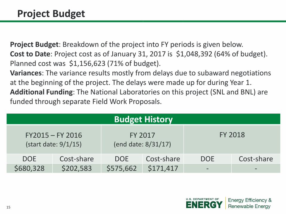
Project Budget: Breakdown of the project into FY periods is given below.Cost to Date: Project cost as of January 31, 2017 is $1,048,392 (64% of budget). Planned cost was $1,156,623 (71% of budget).Variances: The variance results mostly from delays due to subaward negotiations at the beginning of the project. The delays were made up for during Year 1.Additional Funding: The National Laboratories on this project (SNL and BNL) are funded through separate Field Work Proposals.
Budget History
FY2015 – FY 2016(start date: 9/1/15)
FY 2017(end date: 8/31/17)
FY 2018
DOE Cost-share DOE Cost-share DOE Cost-share$680,328 $202,583 $575,662 $171,417 - -
Project Budget

16
Project Plan and Schedule
Incurred a 3-4 month delay waiting for approval of CRADAs with National Laboratories Lumileds/MIT efforts started on schedule, but majority of work delayed until contract approval,
resulting in pushout on some of Year 1 milestone completions Year 2 milestones are now caught up to original schedule