radiometric calibration of a hybrid rcwt...
TRANSCRIPT

Radiometric Calibration of a Hybrid RCWT Imaging Model
Item Type text; Electronic Thesis
Authors Pratap Kadam, Poonam
Publisher The University of Arizona.
Rights Copyright © is held by the author. Digital access to this materialis made possible by the University Libraries, University of Arizona.Further transmission, reproduction or presentation (such aspublic display or performance) of protected items is prohibitedexcept with permission of the author.
Download date 18/06/2018 18:25:42
Link to Item http://hdl.handle.net/10150/339045

RADIOMETRIC CALIBRATION OF A HYBRID RCWTIMAGING MODEL
by
Poonam Pratap Kadam
A Thesis Submitted to the Faculty of the
COLLEGE OF OPTICAL SCIENCES
In Partial Fulfillment of the Requirements
For the Degree of
MASTER OF SCIENCE
In the Graduate College
THE UNIVERSITY OF ARIZONA
2 0 1 4

STATEMENT BY AUTHOR
This thesis has been submitted in partial fulfillment of requirements for an ad-vanced degree at The University of Arizona and is deposited in the University Libraryto be made available to borrowers under the rules of the Library.
Brief quotations from this thesis are allowable without special permission, pro-vided that accurate acknowledgment of the source is made. Requests for permissionfor extended quotation from or reproduction of this manuscript in whole or in partmay be granted by the head of the major department or the Dean of the GraduateCollege when in his or her judgement the proposed use of the material is in the in-terests of scholarship. In all other instances, however, permission must be obtainedfrom the author.
SIGNED: Poonam Pratap Kadam
APPROVAL BY THESIS DIRECTOR
This thesis has been approved on the date shown below:
Dr. Thomas D. MilsterProfessor of
Optical Sciences
12/16/2014
Date
3

ACKNOWLEDGMENTS
First and foremost, I am deeply indebted to my advisor Dr. Tom D. Milster,
for the suggestion of this research topic and his dedicated and consistent support,
guidance, and patience with me throughout this project. I simply could not ask for a
better advisor. I also thank Dr. Yuzuru Takashima and Dr. Young-Sik Kim for their
participation on the committee and for their helpful comments.
My sincere thanks also goes to my fellow graduate students, Priyanka, Wanglei,
Thiago, Akira, Weichuan, Cory, Ben, Tyler, Lee, Melissa and Kaitlyn, for all the
conversations, advice and assistance. I also would like to thank everyone else in our
group for their support. I am extremely fortunate to have had the opportunity to
work with this group.
I am grateful to my friends (too many to list here but you know who you are!)
both near and far for being my family away from home. Thank you for listening,
supporting me and being just a phone call/text away. Special thanks to my two
lovely roommates for all their love, patience and delicious food.
Last, but not least, I would like to thank my family for being the single biggest
motivating force in my life. This work would not be complete without their uncondi-
tional love, encouragement and sacrifices. I would like to dedicate this thesis to my
grandparents. Thank you for having faith in me.
4

TABLE OF CONTENTS
LIST OF FIGURES . . . . . . . . . . . . . . . . . . . . . . . . . . . . . . . . 7
LIST OF TABLES . . . . . . . . . . . . . . . . . . . . . . . . . . . . . . . . . 10
ABSTRACT . . . . . . . . . . . . . . . . . . . . . . . . . . . . . . . . . . . . 11
Chapter 1: Introduction . . . . . . . . . . . . . . . . . . . . . . . . . . . . . . 12
Chapter 2: Background . . . . . . . . . . . . . . . . . . . . . . . . . . . . . . 15
2.1 Literature Survey . . . . . . . . . . . . . . . . . . . . . . . . . . . . . 16
2.2 Hybrid RCWT Calculations . . . . . . . . . . . . . . . . . . . . . . . 24
2.3 Partial Coherence in Imaging . . . . . . . . . . . . . . . . . . . . . . 27
2.4 Noise in Low Light Conditions . . . . . . . . . . . . . . . . . . . . . . 29
Chapter 3: Radiometry of Partially Coherent Sources . . . . . . . . . . . . . 33
Chapter 4: Hybrid RCWT Simulations . . . . . . . . . . . . . . . . . . . . . 36
4.1 Diffraction Efficiencies . . . . . . . . . . . . . . . . . . . . . . . . . . 36
4.2 Coherent Imaging . . . . . . . . . . . . . . . . . . . . . . . . . . . . . 37
4.3 Partially Coherent Imaging . . . . . . . . . . . . . . . . . . . . . . . . 39
Chapter 5: Experimental Setup . . . . . . . . . . . . . . . . . . . . . . . . . . 45
5.1 Experimental Setup . . . . . . . . . . . . . . . . . . . . . . . . . . . . 45
5.2 Camera Calibration . . . . . . . . . . . . . . . . . . . . . . . . . . . . 50
5.2.1 Irradiance of Two-beam Interference . . . . . . . . . . . . . . 52
5.3 Calibration of Optical System . . . . . . . . . . . . . . . . . . . . . . 53
5

Chapter 6: Experimental Results . . . . . . . . . . . . . . . . . . . . . . . . . 57
6.1 Coherent Source . . . . . . . . . . . . . . . . . . . . . . . . . . . . . 57
6.2 Partially Coherent Source . . . . . . . . . . . . . . . . . . . . . . . . 60
Chapter 7: Conclusions and Future Work . . . . . . . . . . . . . . . . . . . . 66
7.1 Conclusions . . . . . . . . . . . . . . . . . . . . . . . . . . . . . . . . 66
7.2 Future Work . . . . . . . . . . . . . . . . . . . . . . . . . . . . . . . . 67
APPENDIX A: MATLAB CODE FOR COHERENT IMAGING MODEL . . 70
APPENDIX B: MATLAB CODE FOR PARTIALLY COHERENT IMAGINGMODEL . . . . . . . . . . . . . . . . . . . . . . . . . . . . . . . . . . . . . 75
REFERENCES . . . . . . . . . . . . . . . . . . . . . . . . . . . . . . . . . . . 81
6

LIST OF FIGURES
1-1 MPU Fin and Flash Memory Potential solutions [2] . . . . . . . . . . 13
2-1 Imaging setup used in [25]. For the illumination, P" is the entrancepupil and the corresponding exit pupil is P. For the imaging path, Pand P’ are the entrance and exit pupil respectively. . . . . . . . . . . 17
2-2 (left) Measured Intensity, (right) Computed Intensity of the grooves ofa Si grating in Totzeck [25]. A relative irradiance scale is used in bothcases. . . . . . . . . . . . . . . . . . . . . . . . . . . . . . . . . . . . . 18
2-3 Schematic of the optical imaging model by Török et al. [24]. Thepink block is the calculation of incident light. The second component(blue) discusses the scattering. The third part (white) talks about thecollection. The final element of the model (green) calculates the image. 19
2-4 Image of the pattern ’ ICL’ obtained as the angle of linearly polarisedincident illumination. Central part of ’I’ has a width of 𝜆/2 [24]. . . . 20
2-5 Schematic of the optical imaging system components in Çapoğlu et al.[5]: illumination, scattering, collection, and refocusing . . . . . . . . . 21
2-6 Comparison of FDTD-synthesized and measured bright-field grayscalemicroscope images and pixel spectra for an isolated polystyrene latexbead. Top: 2.1-𝜇m bead; bottom: 4.3-𝜇m bead in Çapoğlu et al. [5]. . 23
2-7 SIL microscope in Yang et al. [28]. . . . . . . . . . . . . . . . . . . . 24
2-8 Normalized irradiance distributions of native polarization at the imageplane. Quartz grating on a quartz substrate and chrome grating on aquartz substrate, duty ratio is 1:1 and substrate is quartz, n𝑄𝑍 = 1.546and n𝐶𝑅 = 2.314 + i3.136 at 550nm, and grating height is 100nm in [28]. 25
2-9 Angle definition for RCWT. 𝜃 is the angle of incidence with respect to zaxis. 𝜑 is the rotational angle about the z axis. 𝜓𝑖𝑛𝑐 is the polarizationangle [27] . . . . . . . . . . . . . . . . . . . . . . . . . . . . . . . . . 26
7

2-10 Abbe theory adapted to the high NA microscope. The light is diffractedfrom the object to form a pattern in the rear focal plane of the lens.Each point in this plane acts as a secondary coherent source whichinterfere with each other to form an image in the image plane [28]. . . 28
2-11 Visibility as a function of spatial frequency for a partially coherentcase 𝜎𝑐. For low spatial frequencies, the image exhibits coherent-likebehavior with three-beam imaging characteristics [12]. . . . . . . . . . 29
2-12 A wafer inspection tool operating at high scan speeds. The imaging ismodeled in RCWT . . . . . . . . . . . . . . . . . . . . . . . . . . . . 32
3-1 Equally spaced sampling of the source at the entrance pupil of thecondenser. Each grid sampling point represents one RCWT calculationwith a plane wave that illuminates the grating at different angles. . . 34
3-2 Radiant flux transfer for an ideal lossless system. A𝑠𝑟𝑐 is the area ofthe source, Ω𝑠𝑟𝑐 and Ω𝑖𝑚𝑔 are the solid angles subtended at the objectand image, respectively, D𝑅𝐿 is the diameter of the relay lens, and 𝑧𝑠𝑟𝑐and 𝑧𝑖𝑚𝑔 are the distances of the source and image from the relay lens. 35
4-1 Schematic of the grating for RCWT simulation. A linearly polarizedplane wave of wavelength 632.8 nm illuminates the grating from theair interface. The grating is a Ronchi ruling with d = 25 𝜇m, DC/d =53% and h = 80 nm. . . . . . . . . . . . . . . . . . . . . . . . . . . . 37
4-2 Reflected diffraction efficiency of the m = 0, ±1 orders. . . . . . . . . 38
4-3 Transmitted diffraction efficiency of the m = 0, ±1 orders. . . . . . . 39
4-4 Radiometrically scaled two-beam irradiance distribution . . . . . . . . 40
4-5 Radiometrically scaled three-beam irradiance distribution . . . . . . . 41
4-6 Radiometrically scaled irradiance distribution modeled in the hybridRCWT calculator. . . . . . . . . . . . . . . . . . . . . . . . . . . . . 42
4-7 Photons/second incident per pixel on the detector . . . . . . . . . . . 43
4-8 SNR for integration time of 1 ms . . . . . . . . . . . . . . . . . . . . 43
4-9 SNR for integration time of 1 𝜇s . . . . . . . . . . . . . . . . . . . . . 44
5-1 The purple and green lines indicate the illumination and image raypaths of the Köhler illumination system. The red lines represent theobject and image conjugate planes. . . . . . . . . . . . . . . . . . . . 46
5-2 Test bench setup for radiometric measurements. . . . . . . . . . . . . 48
5-3 Measurement of pitch and duty cycle under Vecco. . . . . . . . . . . . 49
8

5-4 Calibration constant vs exposure time for the DCC1545M monochromecamera. . . . . . . . . . . . . . . . . . . . . . . . . . . . . . . . . . . 52
5-5 Mach Zender setup to verify the camera calibration constant. . . . . . 54
5-6 Irradiance images captured by the Mach Zender testbench. . . . . . . 55
5-7 Comparison of irradiance obtained from experiment and theory acrossthe same set of points of the image. I1 and I2 are the irradiances of thebeam path 1 and 2, respectively. I𝑒𝑞𝑛 is the max irradiance obtainedfrom Eq. (4.12). I𝑖𝑚𝑔 is the irradiance of the two-beam interferenceimage. . . . . . . . . . . . . . . . . . . . . . . . . . . . . . . . . . . . 56
6-1 Two-beam interference fringe pattern for coherent imaging case. . . . 59
6-2 Three-beam interference fringe pattern for coherent imaging case. . . 60
6-3 Irradiance distribution for two-beam interference. . . . . . . . . . . . 61
6-4 Irradiance distribution for three-beam interference. . . . . . . . . . . 62
6-5 Image of the illumination beam for the coherent imaging case. Theirradiance of the illuminating beam is obtained using the camera cali-bration method. From this image, the incident E field is calculated tobe 410 V/m. . . . . . . . . . . . . . . . . . . . . . . . . . . . . . . . . 62
6-6 Fringe patterns for a partially coherent imaging cases. . . . . . . . . . 63
6-7 Line profile across image plane. . . . . . . . . . . . . . . . . . . . . . 64
7-1 Image quality evaluation using NILS and MEEF with a normalized scale. 69
9

LIST OF TABLES
5.1 Symbols used in the estimation of the camera response . . . . . . . . 50
5.2 Camera parameters that are constant for a given a exposure time . . 53
5.3 Power measurements and transmission constants . . . . . . . . . . . . 54
6.1 Power measurements and diffraction efficiency calculations for trans-mitted and reflected orders. . . . . . . . . . . . . . . . . . . . . . . . 58
6.2 Comparison of results obtained from experiment and simulations . . . 65
7.1 Comparison of results obtained from experiment and simulations afterforcing the diffraction efficiencies to match the experimental results. . 67
10

ABSTRACT
The applications of low-light imaging are widespread in areas such as biomedical
imaging, remote sensing, ratiometric imaging, lithography, etc. The goal of this work
is to develop a radiometrically scaled hybrid RCWT calculator to count the photons
detected for such applications. The rigorous computation of different imaging models
are discussed. An approach to calibrate the radiometry of the hybrid RCWT model
for partially coherent illumination is presented. The diffraction from the object is
evaluated rigorously using the hybrid RCWT model. A test bench is set up to validate
the radiometrically scaled simulations. In all the cases considered, simulation and
experiment agree within a 40% difference.
11

CHAPTER 1
Introduction
The semiconductor industry is driven by speed, reliability, and economy. The world-
wide semiconductor sales for 2013 reached $305.6 billion. The market is forecasted
to be US$350 billion for 2016 [1]. The dimensions of critical features have been con-
stantly scaled down to enhance functionality at lower costs. As reported by Gordon
Moore in [18], the industry has been able to double the number of transistors every
18 months. As shown in Fig. 1-1, The International Technology Roadmap for Semi-
conductors (ITRS) predicts that the flash memory will reach 15 nm by 2015. Larger
wafers increase the productivity by enabling more chips to be fabricated on it. Wafer
sizes are expected to reach 450 mm by 2017. Due to the shrinking critical dimensions,
defects that were overlooked in the previous generations now need to be considered.
Wafer inspection tools are now required to have the resolution and speed to capture
these nano-scale defects. Jota and Milster [9] have proposed an EUVL inspection
tool using a source at Lyman-alpha of Hydrogen at 121.6 nm that has shown to have
significant improvement in inspection resolution compared to ArF (193 nm) and KrF
(248 nm). Due to increased wafer size, inspection tools also need to have faster scan
rates for higher efficiency and productivity. These higher scan rates reduce the time
available to capture photons. At low light conditions, the photon noise, which is
directly proportional to the photons captured, becomes the dominant noise source.
For increased defect sensitivity, the wafer inspection tool must have adequate signal-
to-noise (SNR). Hence, the scan rate is adjusted for sufficient photon count. Other
applications that are SNR sensitive include biomedical imaging, dawn to dusk/night
12

time remote sensing, ratiometric imaging, lithography, etc. Li et al. [11] discuss ra-
diance simulation and measurement at the entrance pupil during satellite run time.
In medical imaging, high light intensities are avoided while working with live cells to
prevent tissue damage.The strong dependence of the roughness of printed lines on the
photons incident per pixel has been examined by Wintz et al. [26]. Hence, there is a
need to rigorously estimate the photons incident on the imaging sensor.
Figure 1-1: MPU Fin and Flash Memory Potential solutions [2]
Classical optical imaging systems have relied on the modelling of the electromag-
netic propagation by ray tracing. Geometrical optics modelling fails with use of micro
or nano structured elements, truncation of fields by apertures, etc. In such cases, a
combination of wave optical modelling and geometrical modelling gives reliable re-
sults. The availability of high-speed computers and the need for improved accuracy
for scientific applications has increased interest in implementing exact solutions to
13

Maxwell’s equations for the rigorous numerical modelling of these systems. Rigorous
numerical electromagnetic methods have been used for numerous important scien-
tific and industrial applications. Examples include integrated circuit inspection [19],
photolithography [6] and bio-photonics [7].
This thesis is primarily focused on the use of a hybrid Rigorous Coupled Wave
Theory (RCWT) model to predict the number of photons captured at the image
plane. The RCWT calculator is a part of the OptiScan software packaged developed
by Milster group. It is used to rigorously model diffraction grating structures. The
history of rigorous coupled wave theory can be traced to Tamir’s work in [22],[21]
and[20]. Moharam and Gaylord used RCWT to model diffraction in dielectric planar
grating diffraction problem [14], surface-relief gratings [13] and metallic gratings [3;
15; 16]. The hybrid RCWT model has been used by Yang et al. [28, 29], Jota et al. [8]
and Zhang et al. [31, 32]. However, these works do not consider the actual power levels
of the source and calculate the relative irradiance values in the image under partially
coherent illumination. The thesis proposed here calibrates the hybrid RCWT model
to accurately predict image irradiance if the source properties are known.
Chapter 2 in this thesis gives a brief background of the methods used to model
electromagnetic propagation through imaging systems. It also discusses partial co-
herence in imaging and noise in low light conditions. The algorithm for imaging using
RCWT is reviewed, and in chapter 3 an appropriate approach to radiometry in partial
coherence is presented. Chapter 4 describes the test bench setup and calculates the
constants required to scale the imaging model. In chapter 5, the hybrid RCWT calcu-
lator is radiometrically scaled, and electromagnetic propagation through an imaging
system is modelled for coherent and partially coherent sources. The results of the ex-
periment are presented and compared to the modeling results in chapter 6. Chapter
7 lists conclusions and future work that can be carried out in this area.
14

CHAPTER 2
Background
Scalar diffraction is valid only when the diffracting objects are large compared to
the wavelength. Scalar diffraction assumes that the exact boundary field distribution
is unknown and makes assumptions about its values. For example, commonly used
diffraction theories for fields diffracted by a slit in an opaque screen assume the fields
inside the opening are the same as the incident fields and are zero elsewhere on the
screen. This assumption is true for an ideal screen, but they are not solutions to
Maxwell’s equations for real slit materials. The magnitude of this error increases as
the width of the slit approaches the wavelength of incident light. Interaction of light
with nano structures yields polarization dependencies, lateral scattered fields, and
excited surface waves. Scalar diffraction theory from an ideal slit cannot account for
these cases.
A practical solution is to rigorously solve Maxwell’s equations by using numer-
ical methods. Various methods exist, such as finite-difference time-domain method
(FDTD), method of moments (MoM), finite-element method (FEM), rigorous coupled
wave theory (RCWA), etc. Vector diffraction theory is used to model anti reflection
structures, polarization gratings, resonant waveguide gratings, high NA lenses, etc. A
comparative study of RCWA, FDTD and FEM is given by Berger et al. [4]. As each
technique has its disadvantages, the numerical method to be used should be chosen
according to the application.
In section 2.1, methods that rigorously simulate imaging from diffractive struc-
15
tures are reviewed. In section 2.2, the hybrid calculations used in this work is dis-
cussed. In section 2.3, partial coherence in imaging is outlined with respect to Köhler
illumination. Finally, section 2.4 reviews noise in low-light conditions.
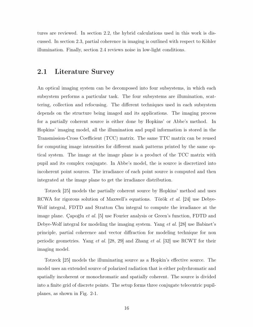
2.1 Literature Survey
An optical imaging system can be decomposed into four subsystems, in which each
subsystem performs a particular task. The four subsystems are illumination, scat-
tering, collection and refocusing. The different techniques used in each subsystem
depends on the structure being imaged and its applications. The imaging process
for a partially coherent source is either done by Hopkins’ or Abbe’s method. In
Hopkins’ imaging model, all the illumination and pupil information is stored in the
Transmission-Cross Coefficient (TCC) matrix. The same TTC matrix can be reused
for computing image intensities for different mask patterns printed by the same op-
tical system. The image at the image plane is a product of the TCC matrix with
pupil and its complex conjugate. In Abbe’s model, the is source is discretized into
incoherent point sources. The irradiance of each point source is computed and then
integrated at the image plane to get the irradiance distribution.
Totzeck [25] models the partially coherent source by Hopkins’ method and uses
RCWA for rigorous solution of Maxwell’s equations. Török et al. [24] use Debye-
Wolf integral, FDTD and Stratton Chu integral to compute the irradiance at the
image plane. Çapoğlu et al. [5] use Fourier analysis or Green’s function, FDTD and
Debye-Wolf integral for modeling the imaging system. Yang et al. [28] use Babinet’s
principle, partial coherence and vector diffraction for modeling technique for non
periodic geometries. Yang et al. [28, 29] and Zhang et al. [32] use RCWT for their
imaging model.
Totzeck [25] models the illuminating source as a Hopkin’s effective source. The
model uses an extended source of polarized radiation that is either polychromatic and
spatially incoherent or monochromatic and spatially coherent. The source is divided
into a finite grid of discrete points. The setup forms three conjugate telecentric pupil-
planes, as shown in Fig. 2-1.
16

Figure 2-1: Imaging setup used in [25]. For the illumination, P" is the entrance pupil
and the corresponding exit pupil is P. For the imaging path, P and P’ are the entrance
and exit pupil respectively.
A rigorous solution of Maxwell’s equations is used when the scattering object is
small when compared to the wavelength. Rigorous Coupled Wave Analysis [RCWA]
is used for the rigorous computations of diffraction fields. The object is assumed to
be periodic. The direction cosines of the diffracted orders are obtained from Floquet
condition. The grating region is divided into layers with the same dielectric constants.
Dielectric constant and fields are expanded as Fourier series for each film.
The diffraction orders obtained from RCWA are coupled together. The enhanced
transmittance matrix approach is used for the projection of the field vectors. The
enhanced transmittance matrix technique is useful in avoiding numerical instabilities
while computing tangential fields. The diffracted orders are propagated and then
filtered at the stop. Only those orders that are less than the illumination NA are
17

allowed to pass through the stop.
The diffracted orders within the imaging NA are summed together. The energy of
the electric field is normalized on the object and image side. The polarization of the
electric field on the image side is converted to global polarization from local polariza-
tion. The irradiance from all source points is summed incoherently to calculate the
total image irradiance at the image plane. The image on the left of Fig. 2-2 shows the
irradiance obtained in measurement from the setup. The image on the right shows
the modeled irradiance distribution.
Figure 2-2: (left) Measured Intensity, (right) Computed Intensity of the grooves of a
Si grating in Totzeck [25]. A relative irradiance scale is used in both cases.
Török et al. [24] uses pairs of lenses in a 4f configuration in the optical setup. The
object is placed at the front focal plane of the first lens. The image field is at the
back focal plane of the second plane. The aperture stop is the common focal plane of
the lens. This system is telecentric from the object and image side. In a homogenous
image space, the electric field is represented as a superposition of plane waves. Con-
siderable spherical aberration occurs when light is focused onto a medium that has a
refractive index different from that of the propagating medium. For a homogeneous
medium, this is solved by the superposition of the refracted plane waves which obeys
Fresnel refraction [23]. From vectorial refraction, a relation between the unit vectors
along a ray in each medium is obtained. The electric field vector is calculated similar
to the homogeneous medium calculation. The aberration introduced by a stratified
media is derived by calculating the aberration by individual layers [23]. The focused
18

field is calculated by the Debye-Wolf integral. The electric field vector is calculated
by the Jones matrix technique. Fig. 2-3 shows the subcomponents of the imaging
system.
Figure 2-3: Schematic of the optical imaging model by Török et al. [24]. The pink
block is the calculation of incident light. The second component (blue) discusses the
scattering. The third part (white) talks about the collection. The final element of
the model (green) calculates the image.
The FDTD method is used to rigorously solve Maxwell’s equations. FDTD eval-
uates how the incident light interacts linearly with the specimen. The electric and
magnetic fields are updated in time using a leap-frog procedure. For each plane
wave incident on the grating, the scattered near fields are calculated using FDTD.
The FDTD is a stable method that does not suffer from matrix inversion problems.
The total-field/scattered-field technique is used to introduce the illumination into the
FDTD grid. The TF/SF formulation is based on the linearity of Maxwell’s equations.
It assumes that the total electric and magnetic fields can be decomposed as the sum
of the incident and scattered fields. The incident fields are assumed to be known at
all time steps. The scattered fields are obtained from the interaction of the incident
fields with the material. The region surrounding the scattering object is divided into
19

two distinct zones which are separated by a virtual surface that generates the incident
wave. The inner region assumes that the Yee algorithm operates on the total field
components. The outer region assumes that the Yee algorithm operates only on the
scattered field components. The FDTD domain is terminated by a boundary condi-
tion. A perfectly matched layer (PML) is a virtual layer surrounding the scattering
region with a low coefficient of reflection.
To avoid high computer memory usage, the scattered field is computed very close
to the scattering object using FDTD. The scattered field is calculated rigorously using
a dense grid. The FDTD method requires at least 20 cells per wavelength. A near-to-
far field transformation is used to resample the data rigorously to a lesser dense grid.
Once the near field is known, the Stratton Chu integral is evaluated to calculate the
fields at any point in space outside the volume containing all sources and sinks.
For a homogeneous medium, Török et al. [24] uses the Stratton Chu integral
to find the geometrical optics approximation of the scattered field on the Gaussian
reference sphere. The Debye-Wolf equation is then used to compute the field at the
image plane. For a stratified medium, 𝑚-theory is used to calculate the geometrical
optics approximation. A wide field image of a pattern etched in gold in show in Fig.
2-4. A wavelength of 𝜆 = 405nm is used along with a 100x, .85 NA objective. It is
observed that the horizontal portion of ’L’ is barely visible due to its sub-wavelength
size.
Figure 2-4: Image of the pattern ’ ICL’ obtained as the angle of linearly polarised
incident illumination. Central part of ’I’ has a width of 𝜆/2 [24].
Çapoğlu et al. [5] uses Kohler illumination to illuminate the experimental system.
20

The light source is imaged onto an aperture stop placed at the front focal length of
a condenser lens. The aperture stop acts as a secondary source which is partially co-
herent. Each point source from the stop creates a collimated beam which illuminates
the object. Köhler illumination is hence an incoherent summation of plane waves.
Fig. 2-5 shows the subcomponents of the imaging system.
Figure 2-5: Schematic of the optical imaging system components in Çapoğlu et al.
[5]: illumination, scattering, collection, and refocusing
The FDTD method is used to solve Maxwell’s equations rigorously. The TF/SF
introduces the plane wave onto the grid. The scattered field is now propagated to the
image plane. The objective collects the scattered light that falls within its entrance
pupil. The system is an object side telecentric system. An object side telecentric
system is one in which the entrance pupil is at infinity. In the far field, the wavefront
at the EP is independent of the radial factor. The strength factor of the ray is
calculated at various points in the observation direction. The far field is calculated
21

from the near using Fourier analysis or Green’s function. If the field is known on a
laterally infinite plane between the object and the entrance pupil, then the strength
factor can be calculated by using the spatial Fourier transform of the near field around
the object. The Green’s function formalism is used for a non-periodic scatterer. The
scattering object is assumed to be located within a closed virtual surface. The fields
at the surface are converted to currents using surface equivalence theorem. These
currents are calculated assuming that the interior is removed. This hence gives the
same far field as originally produced by the scattering object. Due to the far field
approximation, the surface integrals only depend on the observation angles, and r
dependence is factored out.
If the image field is homogeneous, then the vector field is given by the Debye-Wolf
integral. For a stratified medium, the Fresnel refraction is also taken into account as
discussed in the illumination of [6]. Aberrations in the refocusing is considered by the
addition of the phase factor in the Debye-Wolf integral. The spectra of the polystyrene
latex beads obtained from the physical experiment using an objective is compared
to the numerical simulations using FDTD between 486 nm and 589 nm in Fig. 2-
6. The top and bottom row plots are for a 2.1 𝜇m and 4.3 𝜇m bead, respectively.
The plots in the left and center columns show the numerically modelled FDTD and
measured bright-field images, respectively. The plots in the right column compare
the measured and simulated spectra. An optimum focusing depth was chosen for the
numerical modelling of the images since the focal plane position in measurements
were not known.
Yang et al. [28] developed a modelling technique for non periodic geometries using
Babinet’s principle, partial coherence and vector diffraction. A polarized light source
is incident on the object through a high NA objective lens. The illumination and
diffraction occur in high NA, while the components after the stop are operated with
low NA. Hence, the system is evaluated rigorously in illumination and diffraction
and modelled with scalar diffraction before and after the stop. The illumination
and imaging paths are shown in Fig. 2-7. The irradiance from each point source
is calculated and then added together incoherently at the image plane. Babinet’s
principle is compared to the RCWT results in Fig. 2-8.
22

Figure 2-6: Comparison of FDTD-synthesized and measured bright-field grayscale
microscope images and pixel spectra for an isolated polystyrene latex bead. Top:
2.1-𝜇m bead; bottom: 4.3-𝜇m bead in Çapoğlu et al. [5].
Zhang et al. [32] used the setup in Fig. 2-7 for imaging Blu-Ray disk samples.
Third order aberrations by the cover layer of BD are calculated by tracing marginal
and chief rays. This imaging system is rigorously simulated using RCWT that predicts
the experimental image contrast accurately. Yang et al. [29] developed a high NA
imaging model to study the dependencies of contrast versus source polarization angles
for induced and native polarization images. Zhang et al. [31] used RCWT to model
image profile for various gratings with different monopole locations and polarization
states.
23

Figure 2-7: SIL microscope in Yang et al. [28].
2.2 Hybrid RCWT Calculations
For this thesis, simulations use the OptiScan RCWT calculator. Zhang [30] includes
a complete description of the RCWT calculator. It is a very popular computational
method for periodic structures. It can be extended to non-periodic structures by using
a PML [10]. Yang [27] has verified the RCWT calculator and its imaging techniques
by comparing the results to [17] and [25], respectively.
Rigorous coupled wave theory is one of the most commonly used techniques for
rigorously modelling periodic structures. Its accuracy depends on the number of
harmonics that are retained in the calculation. The grating is periodic in the x
direction with a base period d and uniform in the y direction. It is infinite in both
the x and y directions. In the z direction, it is divided into regions based on the index
variation. Fig 2-9 shows the angles used in the calculation.
A plane wave incident on the object due to focussing by an objective lens is given
by
24

Figure 2-8: Normalized irradiance distributions of native polarization at the image
plane. Quartz grating on a quartz substrate and chrome grating on a quartz substrate,
duty ratio is 1:1 and substrate is quartz, n𝑄𝑍 = 1.546 and n𝐶𝑅 = 2.314 + i3.136 at
550nm, and grating height is 100nm in [28].
U𝑖𝑙𝑙(r) = A𝑖𝑙𝑙(k)exp(𝑖k.r), (2.1)
where propagation vector k = 2𝜋𝑛(𝛼x + 𝛽y + 𝛾z )/𝜆, 𝛼, 𝛽 and 𝛾 are the direction
cosines in the x, y and z directions, 𝜆 is the vacuum wavelength and n is the refractive
index of the medium. Direction cosines are defined as 𝛼 = sin𝜃cos𝜑, 𝛽 = sin𝜃sin𝜑 and
𝛾 = (1- 𝛼2-𝛽2)1/2. p and s are defined with 𝜓𝑖𝑛𝑐 = 0𝑜 and 𝜓𝑖𝑛𝑐 = 90𝑜, respectively.
A𝑖𝑙𝑙(k) =1√
𝛼2 + 𝛽2
⎛⎝−𝛽 𝛼
𝛼 𝛽
⎞⎠A𝑠𝑟𝑐(k)
⎛⎝cos𝜓𝑠𝑟𝑐
sin𝜓𝑠𝑟𝑐
⎞⎠ , (2.2)
where A𝑠𝑟𝑐(k) is the complex amplitude of the plane wave. 𝜙𝑠𝑟𝑐 represents the polar-
ization angle of the plane wave incident on the objective.
The dielectric constant, the electric and magnetic fields are expressed as a Fourier
25

Figure 2-9: Angle definition for RCWT. 𝜃 is the angle of incidence with respect to z
axis. 𝜑 is the rotational angle about the z axis. 𝜓𝑖𝑛𝑐 is the polarization angle [27]
series. Due to the periodicity of the grating, the Floquet condition is applied to
the fields. When a single plane wave U𝑖𝑙𝑙 is incident on the grating, the normalized
reflectance and transmittance with respect to s and p polarization are calculated by
RCWT for all the diffraction orders and stored in U𝑅,𝑚. The direction cosine of
diffracted order m from the Floquet condition is given by
𝑛𝛼𝑚 = 𝑛𝛼−𝑚(𝜆/𝑑). (2.3)
The total reflected field U𝑅(r) is the sum of the diffracted orders given by,
U𝑅(r) =∑𝑚
U𝑅,𝑚exp[𝑖k(𝛼𝑚x + 𝛽y + 𝛾𝑚z )], (2.4)
26

where 𝛾𝑚 =√
1 − 𝛼2𝑚 − 𝛽2.
The diffracted orders are spatially filtered at the stop and recombined to form an
image at the image plane that is described as
U𝑖𝑚𝑎𝑔𝑒(𝑟′) =
∑𝑚
U𝑚,𝑖𝑚𝑎𝑔𝑒exp(𝑖k𝑖𝑚𝑎𝑔𝑒.r’), (2.5)
and
k𝑖𝑚𝑎𝑔𝑒 =2𝑛
𝜆(𝛼𝑚+ 𝛽𝑦 −
√𝑚2
𝑇 − 𝛼2𝑚 − 𝛽2). (2.6)
While U𝑚,𝑅 is described in local s and p polarization, it needs to be converted
to global polarization with respect to x and y for U𝑚,𝑖𝑚𝑎𝑔𝑒. The illumination electric
field and diffracted orders are normalized for energy conservation. Taking these factors
into account and assuming that the image is a long conjugate without significant z
component,
⎛⎝𝑈𝑚,𝑖𝑚𝑎𝑔𝑒,𝑥
𝑈𝑚,𝑖𝑚𝑎𝑔𝑒,𝑦
⎞⎠ =𝑅𝑒[
√𝛾𝑚/𝛾]√
𝛼2 + 𝛽2
⎛⎝−𝛽 𝛼
𝛼 𝛽
⎞⎠⎛⎝𝑈𝑅,𝑚,𝑠
𝑈𝑅,𝑚,𝑝
⎞⎠ . (2.7)
The irradiance from all the point sources are summed incoherently to calculate
the image,which is given by
I𝑖𝑚𝑎𝑔𝑒(r′) = 𝐶𝑖
∑𝛼,𝛽
|U𝑖𝑚𝑎𝑔𝑒(r′)|2, (2.8)
where C 𝑖 is a constant that is determined in this work as a function of the partial
coherence and sampling of the illumination of the objective lens.
2.3 Partial Coherence in Imaging
When an incoherent light source has a finite spatial extent, each point illuminates the
object incoherently. The size of the light source determines the range of angles illumi-
nating the object. This is known as partial coherence. Partially coherent illumination
is most commonly obtained by the Kohler illumination technique. The optical scheme
27

of a high NA microscope based on the Abbe theory of imaging is shown in Fig. 2-10.
The image fromed at the image plane can be visualized as an incoherent summation
of all the intensities of the individual point sources. The degree of partial coherence
is a measure of how much of the entrance pupil is filled up by the illuminating beam.
It is defined as
𝜎𝑐 =𝐷𝑠
𝐷𝐸𝑝
, (2.9)
where D𝑠 and D𝐸𝑝 are diameters of the image of the source on the entrance pupil
and of the entrance pupil, respectively. Fig. 2-11 shows the visbility as a function of
the spatial frequency for a partially coherent case of 𝜎𝑐 = 0.35.
Figure 2-10: Abbe theory adapted to the high NA microscope. The light is diffracted
from the object to form a pattern in the rear focal plane of the lens. Each point in
this plane acts as a secondary coherent source which interfere with each other to form
an image in the image plane [28].
The visibility of the image is,
𝑉 =𝐼𝑚𝑎𝑥 − 𝐼𝑚𝑖𝑛
𝐼𝑚𝑎𝑥 + 𝐼𝑚𝑖𝑛
, (2.10)
where I𝑚𝑎𝑥, I𝑚𝑖𝑛 are the maximum and minimum irradiance at the image, respec-
tively.
At low spatial frequencies, the first orders overlap completely at the aperture stop
and transmit through it. Hence, the visibility is 1 and continues to be until the first
orders reach the edge of the aperture, which is where
28

𝜂𝑒𝑑𝑔𝑒 = (1 − 𝜎𝑐)𝑁𝐴/𝜆. (2.11)
At this spatial frequency, the image contrast decreases. The visibility is given by
the ratio of the overlap area of the first orders in the pupil to the area of the zero
order. It continues to decrease until the first orders fall just outside the aperture,
where
𝜂𝑚𝑎𝑥 = (1 + 𝜎𝑐)𝑁𝐴/𝜆. (2.12)
Beyond 𝜂𝑚𝑎𝑥, the visibility is zero as only the zero order is transmitted through
the stop.
Figure 2-11: Visibility as a function of spatial frequency for a partially coherent
case 𝜎𝑐. For low spatial frequencies, the image exhibits coherent-like behavior with
three-beam imaging characteristics [12].
2.4 Noise in Low Light Conditions
Light is a collection of photons propagating through space. Each photon contains a
certain amount of energy. The photon energy depends on the carrier frequency as
𝑄 = .𝑤 =ℎ
𝑇=ℎ𝑐
𝜆, (2.13)
29

where ℎ = 6.626e−34 Js denotes the Planks constant and c = 2.99e8 m/s is the speed
of light.
𝑄 =19.865e−17
𝜆 [nm]𝐽/𝑝ℎ𝑜𝑡𝑜𝑛. (2.14)
The same expression in eV reads,
𝑄[𝑒𝑉 ] =1.239𝑒𝑉
𝜆 [𝜇m]. (2.15)
The number of photons N per Joule is
𝑁
𝑄=
𝜆 [nm]19.865e−17
𝑝ℎ𝑜𝑡𝑜𝑛𝑠/𝐽. (2.16)
Since 1 J/s corresponds to a radiant flux of 1W, the number of photons per second
from a source with power W is,
𝑁
𝜑= 5.034𝑒15𝑊𝜆[nm] 𝑝ℎ𝑜𝑡𝑜𝑛𝑠/𝑠. (2.17)
In terms of the irradiance, the number of photons per pixel is given by
𝑁
𝜑= 5.034𝑒15𝐼𝐴𝜆[nm] 𝑝ℎ𝑜𝑡𝑜𝑛𝑠/𝑠, (2.18)
where I is the irradiance per pixel and A is the area of one pixel.
The probability that the incident photon is converted to a photo-electron depends
on the quantum efficiency of the detector. The photo-electrons are accumulated in
potential wells. The image readout is completed by counting these photo-electrons.
Noisy images at low light conditions can be explained by the quantum nature of
light. Noise is defined as the uncertainty in a signal due to random fluctuations.
The number of photons emitted by the source per unit time is given by the Poisson
distribution. The probability of observing n photons is,
𝑃 (𝑛|𝑛) = 𝑒−𝑛𝑛𝑛
𝑛!, (2.19)
where 𝑛 is the mean number of photons arriving per unit time. The standard deviation
of a poisson distribution is equal to the square root of the mean
30

𝜎𝑛 =√𝑛. (2.20)
The signal-to-noise is hence given by
𝑆𝑁𝑅𝑝𝑜𝑖𝑠𝑠𝑜𝑛 =𝑛
𝜎𝑛=
√𝑛. (2.21)
The SNR of the image increases with an increasing number of photons per pixel.
The SNR of the image can be increased by increasing the intensity of incident light
or by increasing the exposure time. For a detector with with quantum efficiency Q,
and integration time t, the SNR is
𝑆𝑁𝑅𝑝𝑜𝑖𝑠𝑠𝑜𝑛 =√𝑄𝑡𝑛. (2.22)
Wafer inspection tools are critical in detecting defects that may occur during an
IC fabrication. While the critical dimensions have shrunk, the area of the wafers has
increased. The key to maintaining a high throughput is to capture these defects over
the entire area of the wafer in the least possible time. Hence, there is a need for high
scan rates for inspection tools as shown in Fig. 2-12. However, increasing the speed
of the scan reduces the SNR, because there is less light (fewer photons) per pixel for
each object feature. Therefore, the RCWT must be calibrated to estimate the true
power in the image.
31

Figure 2-12: A wafer inspection tool operating at high scan speeds. The imaging is
modeled in RCWT
32

CHAPTER 3
Radiometry of Partially Coherent
Sources
Partial coherence is a crucial aspect of lithography and microscopy. Different partial
coherence values represented by 𝜎𝑐 are used to print different sized features across a
semiconductor chip. 𝜎𝑐 also affects the depth of focus and image contrast of the image.
A novel approach to the radiometric measurement of partially coherent illumination
is proposed here.
The light source is imaged onto the entrance pupil of the condenser by a field lens.
The degree of partial coherence is a measure of how much the entrance pupil of the
system is filled by the image of the source. For modeling the system in RCWT, the
beam at the entrance pupil is divided into a discrete number of point sources N𝐸𝑃 ,
as shown in Fig. 3-1. The quantity N𝐸𝑃 is the number of point sources that fall
within the imaging NA. Every point source illuminates the grating with a collimated
beam from a different direction. Each point source is modeled as a plane wave with
direction cosines 𝛼 = sin𝜃cos𝜑 and 𝛽 = sin𝜃sin𝜑.
The equally spaced point sources at the entrance pupil give rise to equally spaced
direction cosines at the rear focal plane of the condenser. The total power of the
illuminating beam at the entrance pupil is assumed to be 𝜑𝑡𝑜𝑡𝑎𝑙. The power of each
point source is approximately
𝜑𝑠𝑟𝑐 =𝜑𝑡𝑜𝑡𝑎𝑙
𝑁𝐸𝑃
. (3.1)
33

Figure 3-1: Equally spaced sampling of the source at the entrance pupil of the con-
denser. Each grid sampling point represents one RCWT calculation with a plane
wave that illuminates the grating at different angles.
The area of illumination on the object for each sampling grid point is assumed to be
the same as with coherent beam illumination (𝜎𝑐 = 0). The irradiance at the object
for each grid point is
𝐼𝑠𝑟𝑐 =𝜑𝑡𝑜𝑡𝑎𝑙
𝑁𝐸𝑃𝐴𝑐𝑜ℎ
, (3.2)
where A𝑐𝑜ℎ is the area of the coherent beam at the object. Once the irradiance of
each point source is known, the electric field amplitude of each grid is given by
𝐸𝑠𝑟𝑐 =
√2𝜑𝑡𝑜𝑡𝑎𝑙
𝑁𝐸𝑃𝐴𝑐𝑜ℎ𝑐𝜖0(3.3)
where c is the speed of light in vacuum and 𝜖0 is the vacuum permittivity. Using
E 𝑠𝑟𝑐, the irradiance of each point source from RCWT is scaled appropriately and
then summed incoherently at the image plane.
Fig. 3-2 shows a simple image forming system for radiant flux transfer. The relay
lens forms an image of the light source at the entrance pupil of the objective. The
diameter of the relay lens D𝑅𝐿 determines the solid angle at the object and image.
The solid angle subtended at the object and image is
34

Figure 3-2: Radiant flux transfer for an ideal lossless system. A𝑠𝑟𝑐 is the area of
the source, Ω𝑠𝑟𝑐 and Ω𝑖𝑚𝑔 are the solid angles subtended at the object and image,
respectively, D𝑅𝐿 is the diameter of the relay lens, and 𝑧𝑠𝑟𝑐 and 𝑧𝑖𝑚𝑔 are the distances
of the source and image from the relay lens.
Ω𝑠𝑟𝑐 =𝜋𝐷2
𝑅𝐿
4𝑧2𝑠𝑟𝑐, (3.4)
and
Ω𝑖𝑚𝑔 =𝜋𝐷2
𝑅𝐿
4𝑧2𝑖𝑚𝑔
, (3.5)
respectively. If L is the radiance of the object, then the radiant flux at the input
is
𝜑𝑠𝑟𝑐 = 𝐿𝐴𝑠𝑟𝑐Ω𝑠𝑟𝑐, (3.6)
where 𝐴𝑠𝑟𝑐 is the area of the source. Assuming that there are no losses between the
source and the image, the image radiant flux is
𝜑𝑖𝑚𝑔 = 𝜑𝑠𝑟𝑐 = 𝐿𝐴𝑠𝑟𝑐Ω𝑠𝑟𝑐. (3.7)
As 𝜑𝑖𝑚𝑔 = 𝜑𝑡𝑜𝑡𝑎𝑙, Eq. 3.3 can be written as
𝐸𝑠𝑟𝑐 =
√2𝐿𝐴𝑠𝑟𝑐Ω𝑠𝑟𝑐
𝑁𝐸𝑃𝐴𝑐𝑜ℎ𝑐𝜖0. (3.8)
35

CHAPTER 4
Hybrid RCWT Simulations
This chapter discusses the results obtained from the hybrid RCWT calculator. First,
the diffraction efficiencies of the transmitted and reflected diffracted orders are com-
puted. Then the irradiance distributions for the 𝜎𝑐 = 0, 0.39, 0.52 and 0.65 are
modeled.
4.1 Diffraction Efficiencies
The RCWT calculator is used to calculate the diffraction efficiencies of the plane waves
diffracted by the Ronchi ruling. Fig. 4-1 shows a schematic of the grating period used
in the calculation. The grating has a pitch d of 25 𝜇m, duty cycle DC/d = 53% and
height h of 80 nm. The grating is illuminated by a plane wave of wavelength 632.8
nm and polarization at near normal incidence from the air interface. The complex
reflection and transmission amplitude coefficients are used to calculate the diffraction
efficiencies. Diffraction efficiency is the fraction of the input light diffracted into that
particular order. The reflected and transmitted diffraction efficiencies for near normal
incidence obtained using RCWT are shown in Fig. 4-2 and Fig. 4-3, respectively.
36

Figure 4-1: Schematic of the grating for RCWT simulation. A linearly polarized
plane wave of wavelength 632.8 nm illuminates the grating from the air interface.
The grating is a Ronchi ruling with d = 25 𝜇m, DC/d = 53% and h = 80 nm.
4.2 Coherent Imaging
The computed complex reflection amplitude coefficients are used to calculate the im-
age of the grating for 𝜎𝑐 = 0 as described in the previous chapters. A large number of
orders are needed for accurate simulations when modeling metal gratings. Generally,
m = 2NA𝑖𝑚𝑔𝜆/d orders are used. In this case, 80 orders are taken into account while
performing the calculation. The reflected diffracted orders are propagated, filtered at
the pupil plane and then interfere to form an image. RCWT computes the normalized
irradiance distribution of the image using an electric field of 1 V/m for the amplitude
of the normally incident plane wave illuminating the object. But, as measured from
the test bench, the average electric field incident on the grating is E = 410 V/m.
The irradiance at the image plane is scaled by constants C𝑐𝑎𝑚, C𝑇𝐶 and the system
magnification m𝑇 . The irradiance at the image plane is
37

Figure 4-2: Reflected diffraction efficiency of the m = 0, ±1 orders.
𝐼𝑡 =1
2𝑚2𝑇
𝑐𝜖0𝐶𝑐𝑎𝑚𝐶𝑇𝐶𝐸2𝐼𝑐, (4.1)
where c is the speed of light in vacuum, 𝜖0 is the vacuum permittivity, m𝑇 is the
transverse magnification, I 𝑐 is the irradiance computed for an E field of 1 V/m and
I 𝑟 is the true irradiance of the image.
Figures 4-4 and 4-5 show the radiometrically scaled irradiance plots for two and
three-beam interference, respectively.
For the two-beam interference, the DC component is blocked from getting to the
CCD. Hence, the cosine image is centered about the x-axis. The absolute value of
the energy field gives double the frequency of the original cosine image. This effect is
not observed in a two-beam interference with the 0 and one of the first orders. The
three-beam irradiance pattern shows a clear drop in visibility.
38

Figure 4-3: Transmitted diffraction efficiency of the m = 0, ±1 orders.
4.3 Partially Coherent Imaging
The approach mentioned in Chap. 3 is used to obtain the real irradiance distibution
at the image plane for 𝜎𝑐 = 0.39, 0.52 and 0.65. The image irradiance due to each
sample point of the source is
𝐼𝑖𝑚𝑔,𝑠𝑟𝑐 = 𝐸2𝑠𝑟𝑐𝐼𝑐, (4.2)
where E𝑠𝑟𝑐 is obtained from Eq. 3.8, and I𝑐 is the irradiance calculated from RCWT
for each point source. The irradiance is then summed incoherently and scaled as
𝐼𝑡 =1
2𝑚2𝑇
𝑐𝜖0𝐶𝑐𝑎𝑚𝐶𝑇𝐶
∑𝑁𝐸𝑃
∑𝑚
𝐼𝑖𝑚𝑔,𝑠𝑟𝑐, (4.3)
where c is the speed of light in vacuum, 𝜖0 is the vacuum permittivity, m𝑇 is the
transverse magnification, m is the order, 𝑁𝐸𝑃 I𝑖𝑚𝑔,𝑠𝑟𝑐 is the irradiance computed for
each point source and I𝑟 is the true irradiance of the image. The plots of the true
irradiance distributions for 𝜎𝑐 values of 0.39, 0.52 and 0.65 are shown in Fig. 4-6.
39

Figure 4-4: Radiometrically scaled two-beam irradiance distribution
From Eq. (2.18), the number of photons per pixel per second for 𝜎𝑐 = 0.39 is
shown in Fig. 4-7
The DCC1545M monochrome camera has a quantum efficiency Q of 50% at 632.8
nm. For integration times of 1 ms and 1 𝜇s, Figures 4-8 and 4-9 show the line profile
of the SNR.
40

Figure 4-5: Radiometrically scaled three-beam irradiance distribution
41

(a) 𝜎𝑐 = 0.65
(b) 𝜎𝑐 = 0.52
(c) 𝜎𝑐 = 0.39
Figure 4-6: Radiometrically scaled irradiance distribution modeled in the hybrid
RCWT calculator.
42

Figure 4-7: Photons/second incident per pixel on the detector
Figure 4-8: SNR for integration time of 1 ms
43

Figure 4-9: SNR for integration time of 1 𝜇s
44

CHAPTER 5
Experimental Setup
This chapter discusses the setup used for the coherent and partially coherent case in
the experiment. A technique to map the pixel values to true irradiance measurements
is explained. Finally, a constant to account for the losses of the system is calculated.
5.1 Experimental Setup
The illumination technique used to satisfy the Abbe imaging requirements is the
Köhler illumination, as shown in Fig. 5-1. In this technique, each point in the light
source is imaged by the auxiliary lens to the condenser aperture plane. The condenser
aperture is the front focal length of the condenser lens, hence collimated beam is
sent through the object plane. The beam in the condenser aperture is treated as a
collection of individual point sources. The spatial coherence of the beam is varied
by changing the fill of the beam at the aperture. If the diameter of the beam at
the aperture is very small, the illumination is treated as a single point source which
illuminates the object with a single plane wave. This forms a coherent imaging
system. When the diameter of the illumination spot at the aperture increases, the
spatial coherence decreases. This is due to the object being illuminated by multiple
plane waves. The system is spatially incoherent when the plane waves fill up the NA
of the objective. Since the illumination on the object is an incoherent summation of
plane waves, it is independent of the fluctuations in the source intensity.
45

Figure 5-1: The purple and green lines indicate the illumination and image ray paths
of the Köhler illumination system. The red lines represent the object and image
conjugate planes.
The incident plane waves are diffracted by the object, and the diffraction pattern
is formed at the rear focal plane of the objective. The zero order beam travels parallel
to the optical axis and is focussed at the rear focus. The other orders are focussed
on either side of the optical axis. The spacing of the higher orders depends on the
pitch of the grating object and the wavelength of the light used. These focussed
spots are the Fourier transform of the image. The diffracted beams now interfere and
form an image at the image plane of the objective. At least two diffracted orders are
required to interfere to form an image. The NA of the imaging lens determines the
quality of the image formed. The larger the NA, the greater number of orders are
combined. The bright and dark pattern at the image place is due to the constructive
and destructive interference of the diffracted orders.
The source is a randomly polarized He-Ne laser with a wavelength of 632.8 nm
46

that is adjusted for height and angle to align it parallel to the optical bench. The
test bench setup is shown in Fig. 5-2. The light emitted by the He-Ne laser is fo-
cussed onto a rotating diffuser by an objective lens (10X, 0.25NA). After transmitting
through the diffuser, the light is scattered into many spots with each one acting as
a quasimonochromatic point source. Due to the rotation of the diffuser, these point
sources move and change randomly. The intensity of light hence appears to be uni-
formly distributed. As the distance between the objective and the rotating ground
glass is increased, the size of the laser beam on the diffuser is increased,which in turn
increases the random phase fluctuations resulting in the area of the plate illuminated
by the laser forming an extended, quasi-monochromatic, incoherent source.The par-
tial coherence 𝜎𝑐 can be varied by changing the distance between the objective and
the rotating ground glass diffuser. A smaller laser spot produces lower 𝜎𝑐.
An iris is placed after the diffuser to control the size and power of the beam
through the system. The beam is then passed through a polarizer to convert the ran-
domly polarized beam to linear polarization. Lens L1 is used to collimate the beam.
Achromatic doublet lenses are used throughout the imaging system, since they have
significantly better optical performance than simple lenses. When operating at infinite
conjugates, the spherical aberration and coma is minimized. The correct orientation
of the achromat is to have the curved surface face the infinite conjugate. The colli-
mated beam is now incident on a 50:50 beamsplitter. The transmitted beam forms
the illumination path of the optical system. The entrance pupil of the illumination
path is at the front focal plane of the condenser lens that is imaged to the rear focal
plane of objective lens L2. The condenser lens is a microscope objective (10X, 0.27
NA), which illuminates the object with a collimated beam. The object is a precision
Ronchi ruling glass slide with 40 lines/mm. The diffracted orders enter the imaging
path. The imaging path forms a 4-f system with lens L1 and the objective before
the beam splitter. On reflection from the beamsplitter, the beam enters another 4-f
optical system formed by lenses L2 and L3. The rear focal plane of L2 coincides with
front focal plane of lens L3. The beam block at the pupil plane, which is conjugate
to the microscope objective stop, filters the diffracted orders to allow transmission
of the m= -1, 0 and +1 orders. For two-beam imaging, the zero order is blocked.
The orders interfere to form an image of the object on a CMOS camera at the image
47

Figure 5-2: Test bench setup for radiometric measurements.
plane.
The grating object is characterized by the Wyko NT9800 interferometer by Veeco
Instruments Inc. It is a non-contact surface profiler working on the principle of white
light interferometry. The object is a chrome grating on a soda lime substrate.The
grating has a d = 25 𝜇m, DC/d = 53% and h = 80 nm as shown in Fig. 5-3. The
achromats in the setup are chosen according to the magnification required at the
image plane. The focal lengths of lens 1, 2 and 3 are 170 mm, 330 mm and 450 mm,
respectively. The magnification of the objective is given by
48

Figure 5-3: Measurement of pitch and duty cycle under Vecco.
𝑀𝑜 =tube length focal length(𝐹𝑡)
objective focal length(𝐹𝑜𝑏𝑗). (5.1)
With a tube length of 160 mm, the objective focal length is 16 mm. The magnification
of the image at the CCD is given by
𝑀𝑡 = 𝑀𝑎 ×𝑀𝑏. (5.2)
Due to the configurations of the illuminating and imaging paths, the magnifications
are
𝑀𝑎 = −𝑓3𝑓2
= 1.37, (5.3)
and
𝑀𝑏 = − 𝑓1𝑓𝑜𝑏𝑗
= 10.63. (5.4)
Hence, the magnification at the imaging plane is 1.37×10.63 = 14.5.
49

5.2 Camera Calibration
A critical step in the measurement of irradiance is the radiometric calibration of the
camera used to capture the images. A constant camera response is required to map
the irradiance to pixel values for specific camera settings. The DCC1545M is an 8
bit monochrome camera with a pixel array of 1280H x 1024V. The size of each pixel
is 5.2 𝜇m x 5.2 𝜇m. An S122C power head and a PM200 handheld power console
are used to make the power measurements. The setup described in Fig. 5-2 is used
to calibrate the camera. An iris is placed just before the image plane. The iris is
sized to prevent overfilling of both the power meter and the CMOS camera. Since the
active sensor area of the power meter is smaller than the camera sensor area, the iris
is sized smaller than the power meter. At the pupil plane, the beam block is designed
to allow only one order to pass through at a time. At the image plane, the camera
and power meter are alternated to capture and measure the diffracted order that is
passed through. The images of the various diffracted orders are captured at the same
exposure parameters. The mathematical formulas given below follows the notation
given in Table 5.1.
Symbol Description
grey level value of pixel at 𝑖, 𝑗𝑞𝑖,𝑗 𝑞 ∈ [0,255] for an 8 bit camera
𝑖, 𝑗 pixel index
𝑃𝑚𝑒𝑡𝑒𝑟 Power in 𝑊 detected by power meter
𝐼𝑖,𝑗 Irradiance in 𝑊/𝑚2 at pixel 𝑖, 𝑗
Table 5.1: Symbols used in the estimation of the camera response
It is desired to find a camera constant C 𝑐𝑎𝑚 such that
𝐼𝑖,𝑗 =𝑞𝑖,𝑗𝐶𝑐𝑎𝑚
. (5.5)
It is known that,
50

∑𝑖,𝑗
𝑞𝑖𝑗∑𝑖,𝑗
𝑞𝑖,𝑗= 1. (5.6)
Multiplying both sides by P𝑚𝑒𝑡𝑒𝑟
𝑃𝑚𝑒𝑡𝑒𝑟 ×∑𝑖,𝑗
𝑞𝑖𝑗∑𝑖,𝑗
𝑞𝑖,𝑗= 𝑃𝑚𝑒𝑡𝑒𝑟 × 1, (5.7)
and ∑𝑖,𝑗
𝐼𝑖,𝑗 × area of pixel = 𝑃𝑚𝑒𝑡𝑒𝑟. (5.8)
Equating Eq. (5.7) and (5.8),
∑𝑖,𝑗
𝐼𝑖,𝑗 × area of pixel =∑𝑖,𝑗
𝑃𝑚𝑒𝑡𝑒𝑟 ×𝑞𝑖𝑗∑
𝑖,𝑗
𝑞𝑖,𝑗. (5.9)
Cancelling summation on both sides and rearranging results in
𝐼𝑖,𝑗 =𝑃𝑚𝑒𝑡𝑒𝑟
area of pixel× 𝑞𝑖𝑗∑
𝑖,𝑗
𝑞𝑖,𝑗. (5.10)
The calibration constant is then
𝐶𝑐𝑎𝑚 =
∑𝑞𝑖𝑗 × area of pixel
𝑃𝑚𝑒𝑡𝑒𝑟
. (5.11)
The irradiance per pixel is given by,
𝐼𝑖,𝑗 =𝑞𝑖,𝑗𝐶𝑐𝑎𝑚
. (5.12)
The calibration constant 𝐶𝑐𝑎𝑚 is calculated for 50 images captured at a particular
exposure time and then averaged out. At 7.009 ms, the calibration constant is 8.336
𝑚2/𝑊 . This procedure is repeated for various sets of images captured at different
exposure times. The calibration constants obtained from these images are plotted
51

Figure 5-4: Calibration constant vs exposure time for the DCC1545M monochrome
camera.
in Fig. 5-4. As seen in the plot, the calibration constants obtained closely follow a
linear trend.
While capturing images with the CCD, care should be taken to ensure that the
images are not saturated. The saturation can be handled by reducing the exposure
time. All the other parameters of the CCD are kept constant and is shown in Table.
5.2. Neutral density filters can also be used to prevent the oversaturation of the CCD.
5.2.1 Irradiance of Two-beam Interference
A simple Mach Zender test bench is setup to compare the intensity of the fringe pat-
tern at the image plane to the intensity of the irradiance calculated by the individual
beam irradiances. This check is done to verify if the calibration yields the correct
irradiance values. A schematic of the setup is shown in Fig 5-5. Figures 5-6a and 5-6b
show images of the individual beam paths; Fig 5-6c shows the fringe pattern obtained
at image plane. The three images are calibrated by the procedure mentioned above
to give the irradiance. Irradiances of the two beams are used to obtain the irradiance
at the image plane due to two beam interference using the equation
52

Camera Parameters Value
Pixel clock 25 MHz
Frame rate 10 fps
Gain 1
𝛾 1
Table 5.2: Camera parameters that are constant for a given a exposure time
𝐼 = 𝐼1 + 𝐼2 + 2√𝐼1𝐼2. (5.13)
A comparison between the measured and computed irradiances are plotted in Fig
5-7. It is seen that peaks of the irradiance obtained from the fringe pattern are
matched well with the irradiance obtained from Eq. 5.13.
5.3 Calibration of Optical System
The system transmission is calibrated to account for losses though the lenses and other
optical components. This step is necessary to calculate the diffraction efficiency of
reflected orders at the pupil plane. To calibrate the system, the grating is replaced
by a mirror. The reflectivity of the mirror R is measured to be 93.8%. The beam
power illuminating the mirror 𝜑𝑡𝑜𝑡𝑎𝑙 is measured. This is followed by a measurement
of the beam power reflected by the mirror 𝜑𝑝𝑢𝑝𝑖𝑙 at the pupil plane. The calibration
constant C 𝑇𝐶 required to account for the transmission through the lenses is
𝐶𝑇𝐶 =𝜑𝑝𝑢𝑝𝑖𝑙𝐶𝑙𝑒𝑛
𝑅𝜑𝑡𝑜𝑡𝑎𝑙
, (5.14)
where C𝑙𝑒𝑛 is the transmission through the last lens. Table 5.3 gives the values of the
power measurements and the calculated constants.
53

Figure 5-5: Mach Zender setup to verify the camera calibration constant.
Power measurements/Constants
Value
Reflectivity of mirror 93%
𝜑𝑡𝑜𝑡𝑎𝑙 (𝜇W) 144.01
𝜑𝑝𝑢𝑝𝑖𝑙 (𝜇W) 54.33
C 𝑇𝐶 0.37
Table 5.3: Power measurements and transmission constants
54

(a) Irradiance of beam path 1 (b) Irradiance of beam path 2
(c) Fringe pattern obtained from the
interference of beam path 1 and 2.
Figure 5-6: Irradiance images captured by the Mach Zender testbench.
55

Figure 5-7: Comparison of irradiance obtained from experiment and theory across
the same set of points of the image. I1 and I2 are the irradiances of the beam path 1
and 2, respectively. I𝑒𝑞𝑛 is the max irradiance obtained from Eq. (4.12). I𝑖𝑚𝑔 is the
irradiance of the two-beam interference image.
56

CHAPTER 6
Experimental Results
This chapter presents the experimental results obtained from the test bench. The
diffraction efficiencies of the diffracted orders are measured and compared to the
simulation results. The comparison between the experiments and simulations are
done for the imaging model for 𝜎𝑐 = 0, 0.39, 0.52 and 0.65.
6.1 Coherent Source
For the coherent imaging 𝜎𝑐 ≈ 0, the laser is focussed onto the rotating ground glass
diffuser by the objective. The grating is taken out of the setup to measure the power
𝜑𝑡𝑜𝑡𝑎𝑙 exiting the condenser objective. 𝜑𝑡𝑜𝑡𝑎𝑙 is scaled by the optical transmission
constant to give the power at the pupil plane 𝜑𝑝𝑢𝑝𝑖𝑙. The grating is replaced, and
the power of the transmitted and reflected diffraction orders are measured behind the
grating and at the pupil plane.
Table. 6.1 shows the powers measured in the reflected and transmitted orders. Us-
ing the transmission constants, the diffraction efficiencies are calculated. The diffrac-
tion efficiency is calculated as the fraction of incident light that is diffracted into a
particular order. The diffraction efficiencies of the transmitted and reflected orders
is calculated with respect to the power incident on the grating and the power at the
pupil plane, respectively.
57

Description Power
Power incident on the grating P1(𝜇W) 286.75
Power at the pupil plane P2(𝜇W) 107.44
Power of transmitted orders Power of reflected orders
Power of 0 order (𝜇W) 82.28 Power of 0 order (𝜇W) 10.03
Power of +1 order (𝜇W) 25.18 Power of +1 order (𝜇W) 9.23
Power of -1 order (𝜇W) 25.08 Power of -1 order (𝜇W) 9.47
DE of transmitted orders DE of reflected orders
0 order 28.18 ±0.7% 0 order 7.98 ±1%
+1 order 8.67 ±0.2% +1 order 8.85 ±1.2%
-1 order 8.63 ±0.2% -1 order 8.45 ±0.7%
Table 6.1: Power measurements and diffraction efficiency calculations for transmitted
and reflected orders.
The diffraction efficiency of the reflected and transmitted orders obtained from
a 𝜎𝑐 = 0 experiment and simulations are compared. In transmission, the diffraction
efficiencies of the 0 and ±1 orders obtained from the experiments are almost the same
as the simulation results. But in reflection, there is a discrepancy in the simulation
and experimental results. The numerical modelling predicts a diffraction efficiency
of 5.1% and 15.9% for the ±1 and 0 orders, respectively. From the experiment, the
diffraction efficiencies are measured to be 7.98 ± 1%, 8.85 ± 1.2% and 8.45 ± 0.7%
for the 0, +1 and -1 orders.
At the pupil plane, all the orders except m = 0 and ±1 are filtered out. For
58

two-beam interference, only the ±1 orders are allowed to propagate beyond the pupil
plane. Fig. 6-1 shows the fringe pattern formed due to two-beam interference. Fig.
6-2 shows the three-beam interference fringes due to m = 0 and ±1 diffracted orders.
Figure 6-1: Two-beam interference fringe pattern for coherent imaging case.
Non-uniformity in the irradiance distribution can be observed in Fig. 6-3. To
remedy this issue, various images of the fringes are captured across the area of the
beam. The peaks of the lines profiles across these images are averaged out using the
findpeaks function in MATLAB. The average value and standard deviation of the
two-beam interference peak irradiance is 0.10 ± 0.02 W/m2. This is comparable to
the peak irradiance of 0.08 W/m2 modeled with the RCWT calculator with an error
of 20 ± 20%. A similar procedure is conducted for three-beam interference and the
irradiance profile is shown in Fig. 6-4. The average value and standard deviation of
the peak irradiance are 0.21 ± 0.01 W/m2. The measured peak irradiance is a very
good match to the simulated irradiance of .215 W/m2. The error between the two
measurements is 2.6 ± 4.7%. As the number of pixels and size of each pixel of the
CCD is known, the pitch of the grating measured from Fig. 6-4 is 180.9 𝜇m. The
ratio of this measured pitch to physical grating pitch is identical to the magnification
factor calculated.
59

Figure 6-2: Three-beam interference fringe pattern for coherent imaging case.
The grating is now replaced by the CCD to image the incident beam. The irradi-
ance of the illuminating beam is calculated from Fig. 6-5 using the camera calibration
method. The irradiance of a beam is
𝐼 =1
2𝑐𝜖𝑜|𝐸|2, (6.1)
where c is the speed of light in vacuum, 𝜖0 is the vacuum permittivity and E is
complex amplitude of the electric field.
The average irradiance of the plane wave is measured to be 223.26 W/m2 from the
illumination image captured. Hence, the average electric field incident on the grating
is 410 V/m.
6.2 Partially Coherent Source
The partial coherence 𝜎𝑐 of the system is varied by changing the size of the source on
the ground glass. 𝜎𝑐 is used to manipulate the spread of the diffracted orders. Using
60

Figure 6-3: Irradiance distribution for two-beam interference.
the radiometric concepts in Chap. 3, irradiance measurements are made for images
captured at 𝜎𝑐 values of 0.39, 0.52 and 0.65. For each case, the condenser objective is
removed and the power at the entrance pupil is noted. Fig. 6-6 displays the images
captured by the CCD for different 𝜎𝑐 values. The average irradiance distribution
across the image profile is plotted in Fig. 6-7.
As the area of the fringe pattern at the image plane is quite large, there is a
non-uniformity in the irradiance of the fringes. Hence, many images are captured
and average irradiance value is calculated in MATLAB. The average and standard
deviation of the peak irradiance for 𝜎𝑐 = 0.65 is 0.18 ± 0.008 W/m2, respectively.
This is comparable to the simulation results with an error of 26.83 ± 4.6%. The
average and standard deviation of the irradiance for 𝜎𝑐 = 0.52 is 0.19 ± 0.016 W/m2
that is comparable to the simulation results with an error of 20.9 ± 8.6%. The average
and standard deviation of the irradiance for 𝜎𝑐 = 0.39 is 0.25 ± 0.011 W/m2 that
is comparable to the simulation results with an error of 23.16 ± 4.5%. Table 6.2
summarizes the experimental and modeling results.
61

Figure 6-4: Irradiance distribution for three-beam interference.
Figure 6-5: Image of the illumination beam for the coherent imaging case. The
irradiance of the illuminating beam is obtained using the camera calibration method.
From this image, the incident E field is calculated to be 410 V/m.
62

(a) 𝜎𝑐 = 0.65
(b) 𝜎𝑐 = 0.52
(c) 𝜎𝑐 = 0.39
Figure 6-6: Fringe patterns for a partially coherent imaging cases.
63

(a) 𝜎𝑐 = 0.65
(b) 𝜎𝑐 = 0.52
(c) 𝜎𝑐 = 0.39
Figure 6-7: Line profile across image plane.
64

Description Experiment Simulation Error %
Transmitted diffraction efficiencies
+1 8.67 ± 0.2% 9.3% 7.26 ± 2.31%
0 28.18 ± 0.7% 27.5% 2.41 ± 2.48%
-1 8.63 ± 0.2% 9.3% 7.76 ± 2.32%
Reflected diffraction efficiencies
+1 8.85 ± 1.2% 5.1% 42.37 ± 13.56%
0 7.98 ± 1% 15.9% 99.25 ± 17.66%
-1 8.45 ± 0.7% 5.1% 39.64 ± 8.91%
Peak Irradiance of coherent (𝜎𝑐 ≈ 0) imaging model
Two-beam 0.10 ± 0.02 W/m2 0.08 W/m2 20 ± 20%
Three-beam 0.21 ± 0.01 W/m2 0.215 W/m2 2.38 ± 4.7%
Peak Irradiance of incoherent imaging model
𝜎𝑐 = 0.39 0.25 ± 0.011 W/m2 0.192 W/m2 23.19 ± 4.4%
𝜎𝑐 = 0.52 0.19 ± 0.016 W/m2 0.15 W/m2 21.05 ± 8.6%
𝜎𝑐 = 0.65 0.18 ± 0.008 W/m2 0.132 W/m2 26.66 ± 4.5%
Table 6.2: Comparison of results obtained from experiment and simulations .
65

CHAPTER 7
Conclusions and Future Work
7.1 Conclusions
The coherence properties of an illumination source are of great importance as it affects
the image resolution, contrast and depth of focus. This work was directed to the study
of radiometry in partially coherent illumination. A literature survey of the existing
optical imaging systems is presented. A brief description of the imaging model using
Rigorous Couple Wave Theory (RCWT) is given. An approach to the radiometric
calibration of a partially coherent beam is presented. RCWT is used to rigorously
solve the diffraction from the grating. The illumination at the entrance pupil is
discretized into point sources. Using Abbe’s imaging technique, the irradiance from
each point source is computed and then summed up in the image plane. A test bench
is set up to validate the numerical modeling. Köhler illumination is used to achieve
Abbe imaging. Certain calibration constants are calculated, which are used to scale
the modeling results. The RCWT results are appropriately scaled by the calibration
constants. The results from the experiment are compared to the radiometrically
scaled hybrid RCWT model.
The transmitted diffraction efficiencies from the experiment are in agreement with
the results obtained from the numerical modelling. But there is an inconsistency in the
reflected diffraction efficiencies. The 0 order DE is almost half of what is predicted
by the modelling, while the ±1 orders have diffraction efficiencies almost twice as
66

much as the simulated values. For the two beam imaging case, the difference in the
irradiance of the simulation and experiment is 40%. The irradiance of the three-
beam interference experiment is in good agreement with simulations. The difference
between the experiment and simulation for 𝜎𝑐 = 0.39, 0.52 and 0.65 is within 30%.
Overall, the simulation and experiment show an agreement within a 40% magnitude
of error that demonstrates the use of this system for low-light imaging applications.
7.2 Future Work
The accuracy of the radiometric calibration can be improved by the following two
techniques. In almost all the cases, the simulation results underestimated the irradi-
ance. This could be attributed to the fact that the reflected zero order was measured
lower than the simulation result. To verify this, the diffraction efficiencies in the
RCWT calculator are manually changed to match the diffraction efficiencies mea-
sured from the experiment. The results obtained for the imaging is shown in Table
7.1. The difference in the errors decreases considerably.
Description Experiment Simulation Error %
𝜎𝑐 = 0 (three beam) 0.21 ± 0.01 W/m2 0.212 W/m2 0.09 ± 4.76%
𝜎𝑐 = 0.39 0.25 ± 0.01 W/m2 0.222 W/m2 11.2 ± 4.02%
Table 7.1: Comparison of results obtained from experiment and simulations after
forcing the diffraction efficiencies to match the experimental results.
For the partially coherent imaging model, the illuminating beam is assumed to
be of uniform intensity. The beam at the entrance pupil is discretized into point
sources, where each point source is modeled as a plane wave illuminating the grating.
Taking into account the non-uniformity of the beam, the power of the point sources
can be weighted appropriately. This will further decrease the difference between the
experimental and simulation results.
67

The radiometrically scaled hybrid RCWT calculator can be used in a variety of
low-light imaging applications. One such application is the EUVL mask inspection
tool proposed by Jota and Milster [9]. The imaging system is modeled in RCWT
for partially coherent illumination. Image quality is evaluated by image contrast,
Mask Error Enhancement Factor (MEEF) and Normalized Image Log-Slope (NILS).
A high quality image has a high NILS and a ’V’ profile MEEF as shown in 7-1a
and 7-1b, respectively. The signal to noise ratio needs to be high enough to detect
the signal generated by defects. The SNR is proportional to the photons captured
by the detector which in turn depends on the speed of the tool. Fewer photons are
captured when then the tool moves fast. Hence, the scanning speed of the EUVL
tool is limited by photon flux. But the normalized values in the 7-1 do not give
any information about the SNR of the inspection image. Using the hybrid RCWT
calculator, the number of photons required to capture an image with good SNR image
can be computed. The speed of the inspection tool can be set accordingly.
68

(a) NILS for dipole at 𝜎𝑐
= 0.8, 256 nm mask pitch.
(b) Inspection MEEF for TM, CD-
10%, 0.8 NA, mask pitch = 112 nm.
Figure 7-1: Image quality evaluation using NILS and MEEF with a normalized scale.
69

APPENDIX A
MATLAB Code for Coherent Imaging
Model
%%working
clc;
clear all;
%%
nm = 1e-9; %nanometer
um = 1e-6; %micrometer
mag = -14.5; %Transverse magnification
Ndata_x = 256; % plotting number of data points over a period
E = 410; % E field in V/m
Efieldsq = E*E;
c = 3e8; %speed of light
epsilon = 8.854e-12 %vacuum permittivity
const = .5*c*epsilon; %
tns = .37; % Optical transmission constant
%%
Air = 1.0000; %Refractive index of air
Soda = 1.5216; %Refractive index of air
Cr = 3.1351+3.3101i; %Refractive index of Cr at 632.8 nm
lambda = 632.8*nm;
n_incident = Air; %Refractive index of incident medium
n_substrate = Soda; %Refractive index of substrate
70

n_grating1 = Cr; %Refractive index of grating1
n_grating2 = Air; %Refractive index of grating2
grating_h = 80*nm; %Grating height
period = 25*um; %Grating period 25 um
duty_cycle = [0.25 0.78 1];
%%
%Loading grating paramters
Grating.n1 = n_incident;
Grating.n2 = n_substrate;
Grating.ng1 = n_grating1;
Grating.ng2 = n_grating2;
Grating.h = grating_h;
Grating.d = period;
Grating.cperd = duty_cycle;
%Range in imaging plane
x = linspace(-abs(mag)*n_incident*1*period,abs(mag)*...
n_incident*1*period,Ndata_x+1);
x = x(1:end-1);
%%
pol_angle = 90; % TE polarization
theta = 0; % incident angle
%theta = 0/180*pi;; % incident angle in radians
polarizer_angle = pol_angle/180*pi;
%Amplitude of incident plane wave
Uincident = [ cos(polarizer_angle);
sin(polarizer_angle)];
%Grating Equation
base_alpha = lambda/period;
%Ideally 2*NA_img/base_alpha is OK for max_m but larger number is
%required to improve accuracy
max_m = 80;
%%
%Incident direction cosines
alpha = n_incident*sind(theta); %n*sin(theta)*cos(phi) % why n?
beta = 0;
sigma = sqrt(alpha^2+beta^2);
71

n1 = conj(n_incident); %% look at it again
gamma = sqrt(n_incident.^2 - sigma.^2); %check
theta = acos(real(gamma/n1));
phi = atan2(beta,alpha);
thetain = theta*180/pi;
phiin = phi/pi*180;
%Polarization projection angles for psi input to Conical program
if sigma == 0,
UUsp = [ Uincident(2);
Uincident(1)];
else
TTT = 1/sigma*[ -beta alpha;
alpha beta];
UUsp = TTT*Uincident;
end
%Calculate psi angle with ratio of Us and Up
psiin = atan2(UUsp(1),UUsp(2))/pi*180;
%ConicalRCWT
[Rs,Rp,Ts,Tp] = ConicalRCWT(Grating,max_m,phiin,psiin,thetain,lambda)
m = max_m; % no of orders taken into consideration
Ux = zeros(length(x),1);
Uy = zeros(length(x),1);
Uz = zeros(length(x),1);
Irtot = zeros(length(x),1);
for orders = [1,0,-1],
%Floquet condition
aa = alpha - base_alpha*orders; %OPD for each order w.r.t. incident, 0th order
%gamma of diffracted plane wave
gamma_i = sqrt(n1^2-(aa.^2+beta^2));
%Normalised for energy conservation
C1 = sqrt(real(gamma_i/gamma));
C2 = C1/(n1*1i);
%Calculate the direction of cosines in imag plane
if aa==0 && beta == 0,
O1 = [ C2*Rp(m);
C1*Rs(m),
0];
72

ai = aa/real(n1)/mag;
else
ai = aa/real(n1)/mag;
bi = beta/real(n1)/mag;
si = sqrt(ai^2+bi^2);
ri = sqrt(1-si^2);
%illumination and source polarisation comparision. For highNA
%Transform matrix in imaging system.
t11 = 1-ai^2/(1+ri);
t12 = -ai*bi/(1+ri);
t21 = t12;
t22 = 1-bi^2/(1+ri);
t31 = -ai;
t32 = -bi;
T = [ t11, t12;
t21, t22;
t31, t32];
%converstion matrix from s and p to x and y at the stop
e11 = beta/sqrt(aa^2+beta^2);
e21 = aa/sqrt(aa^2+beta^2);
e12 = e21;
e22 = e11;
E = [ -e11, e12;
e21, e22];
%amplitude of electric field at the stop
Pupil = E* [ C1*Rs(m);
C2*Rp(m)
];
%amplitude of electric field in the image plane
O1 = T*Pupil;
%O2 = Pupil;
end
%Phase of plane wave
Phase = exp(1j*2*pi*(ai*x)/lambda);
%Coherent Sum
Ux = Ux + O1(1).*Phase';
Uy = Uy + O1(2).*Phase';
73

Uz = Uz + O1(3).*Phase';
% end
m = m + 1;
end
%Incoherent sum among different point sources.
Irtot = Irtot + [abs(Ux).^2 + abs(Uy).^2 + ...
abs(Uz).^2];
%Plotting
Irtot1 = Irtot/mag/mag*Efieldsq*const*tns;
figure(56);
V =(max(Irtot)-min(Irtot))/(max(Irtot)+min(Irtot));
plot(x/um,Irtot1,'r');
ylabel('Irradiance')
xlabel('x[um]');
74

APPENDIX B
MATLAB Code for Partially
Coherent Imaging Model
clc;
clear all;
tic;
%%
nm = 1e-9; %nanometer
um = 1e-6; %micrometer
Ndata_x = 256; % plotting number of data points over a period
c = 3e8; %speed of light
epsilon = 8.854e-12 %vacuum permittivity
const = .5*c*epsilon; %
%%
%Enter inputs
mag = -14.5; %Transverse magnification
tns = .37; %Transmission constant of the system
ds = 6; %DIameter of source image at the stop
Air = 1.0000; %Refractive index of air
Soda = 1.5216; %Refractive index of air
Cr = 3.1351+3.3101i; %Refractive index of Cr at 632.8 nm
lambda = 632.8*nm; %Wavelength
lambdan = 632.8; %Wavelength in nm
n_incident = Air; %Refractive index of incident medium
75

n_substrate = Soda; %Refractive index of substrate
n_grating1 = Cr; %Refractive index of grating1
n_grating2 = Air; %Refractive index of grating2
grating_h = 80*nm; %Grating height
period = 25*um; %Grating period 25 um
duty_cycle = [0.25 0.78 1]; %Grating duty cycle
dNA = 0.025; %Delta illumination NA
NA_img = 0.27; %Imaging NA
dp = 15.5; %Diameter of stop
sigma = ds/dp; %Coherence factor
NA_ill = NA_img*sigma; %Illumination NA
ND = 9.654*6.03; % Neutral density factor
Power = 8.27*um; % Power at EP of objective with ND
Power = Power*ND; % Power at EP of objective without ND
Asrc = 2.7652*um; % Area of coherent point source
x = linspace(-abs(mag)*n_incident*1*period,abs(mag)*n_incident*1*period,Ndata_x+1);
x = x(1:end-1);
areap = 5.2*um; %area of pixel of the detector
Q = .5; %Quantum efficiency of the detector
t1 = 1e-3; %Detector integration time t1
t2 = 1e-6; %Detector integration time t2
%%
%Loading grating parameters
Grating.n1 = n_incident;
Grating.n2 = n_substrate;
Grating.ng1 = n_grating1;
Grating.ng2 = n_grating2;
Grating.h = grating_h;
Grating.d = period;
Grating.cperd = duty_cycle;
%%
a = -1.1*NA_img:dNA:1.1*NA_img;
[AA,BB] = meshgrid(a);
RR = sqrt(AA.^2+BB.^2);
%Prepare light source
JJ = double(RR <= NA_ill);
%obtain the array of index within illumination NA
JJindex = find(JJ>0);
Jlen = length(JJindex);
76

%%
% E field for each point source
Psrc = Power/Jlen;
Isrc = Psrc/Asrc;
E = sqrt((2*Isrc)/(c*epsilon));
Efieldsq = E*E;
%%
pol_angle = 90 % 90 and 0 for TE and TM illuminations respectivley
polarizer_angle = pol_angle/180*pi; % Convert deg to rad
%Amplitude of incident plane wave
Uincident = [ cos(polarizer_angle);
sin(polarizer_angle)];
%Grating Equation
base_alpha = lambda/period;
%Ideally 2*NA_img/base_alpha is OK for max_m but larger number is
%required to improve accuracy especially for metal grating.
%max_m = floor(5*2*NA_img/base_alpha);
max_m = 80;
Irtot = zeros(length(x),1);
%%
for ii = 1:length(JJindex),
%Incident direction cosines
alpha = AA(JJindex(ii));
beta = BB(JJindex(ii));
sigma = sqrt(alpha^2+beta^2);
gamma = sqrt(n_incident.^2 - sigma.^2);
theta = acos(gamma/n_incident);
phi = atan2(beta,alpha);
thetain = theta*180/pi;
phiin = phi/pi*180;
%Polarization projection angles for psi input to Conical program
if sigma == 0,
UUsp = [ Uincident(2);
Uincident(1)];
else
TTT = 1/sigma*[ -beta alpha;
alpha beta];
UUsp = TTT*Uincident;
end
77

%Calculate psi angle with ratio of Us and Up
psiin = atan2(UUsp(1),UUsp(2))/pi*180;
%ConicalRCWT
[Rs,Rp,Ts,Tp] = ConicalRCWT(Grating,max_m,phiin,psiin,thetain,lambda);
m = 1;
Ux = zeros(length(x),1);
Uy = zeros(length(x),1);
Uz = zeros(length(x),1);
for orders = -max_m:max_m,
%Floquet condition
aa = alpha - base_alpha*orders;
%Calculate the electric field
% if diffracted plane waves are within imaging NA
if sqrt(aa^2+beta^2) <= NA_img,
n1 = conj(n_incident);
%gamma of diffracted plane wave
gamma_i = sqrt(n1^2-(aa.^2+beta^2));
R = [ Rs(m) 0;
0 Rp(m)];
if aa==0 && beta == 0,
O1 = [ Rp(m)/(n_incident*1j);
Rs(m);
0];
ai = aa/real(n1)/mag;
else
%Calculate the direction of cosines in imag plane
ai = aa/real(n1)/mag;
bi = beta/real(n1)/mag;
si = sqrt(ai^2+bi^2);
ri = sqrt(1-si^2);
t11 = 1-ai^2/(1+ri);
t12 = -ai*bi/(1+ri);
t21 = t12;
t22 = 1-bi^2/(1+ri);
t31 = ai;
t32 = bi;
%Transform matrix in imaging system.
%if mag >>1, T becomes unit matrix
T = [ t11, t12;
78

t21, t22;
t31, t32];
e11 = beta/sqrt(aa^2+beta^2);
e21 = aa/sqrt(aa^2+beta^2);
e12 = e21;
e22 = e11;
%converstion matrix from s and p to x and y
% at the stop
E = [ -e11, e12;
e21, e22];
%Coefficients considerting energy conservation and
% magnetic field normalization
C1 = sqrt(real(gamma_i/gamma));
C2 = C1/(n1*1j);
%amplitude of electric field at the stop
Pupil = E* [ C1*Rs(m);
C2*Rp(m)];
%amplitude of electric field in the image plane
O1 = T*Pupil;
end
%Plane wave without amplitude
%Phase = exp(1j*2*pi*(ai*xx)/lambda);
Phase = exp(1j*2*pi*(ai*x)/lambda);
%Coherent sume from the same point source
Ux = Ux + O1(1).*Phase';
Uy = Uy + O1(2).*Phase';
Uz = Uz + O1(3).*Phase';
end
m = m + 1;
end
%Incoherent sum among different point sources.
Irtot = Irtot + [abs(Ux).^2 + abs(Uy).^2 + ...
abs(Uz).^2]*Efieldsq;
end
%Plotting
%% Plotting irradiance curves
figure(55);
Irtot1 = Irtot/mag/mag*const*tns;
V =(max(Irtot)-min(Irtot))/(max(Irtot)+min(Irtot))
79

plot(x/um,Irtot1,'r');
ylabel('Irradiance')
xlabel('x[um]');
%%
%Plotting photons/sec/pixel curves
figure(57);
photon = 5.034e15*Irtot1*(areap)^2*lambdan;
plot(x/um,photon,'b');
ylabel('photons/pixel/second')
xlabel('x[um]');
%%
%Plotting SNR
figure(58);
plot(x/um,sqrt(photon*Q*t1),'r');
ylabel('SNR')
xlabel('x[um]');
figure(59);
plot(x/um,sqrt(photon*Q*t2),'c');
ylabel('SNR')
xlabel('x[um]');
toc;
80

REFERENCES
[1] Wsts semiconductor market forecast spring 2014. http://www.wsts.org/PRESS/
Recent-News-Release.
[2] Semiconductor industry association, ’international technology roadmap for semi-
conductors (itrs).’. http://www.itrs.net.
[3] WE Baird, MG Moharam, and TK Gaylord. Diffraction characteristics of planar
absorption gratings. Applied Physics B, 32(1):15–20, 1983.
[4] R. Berger, J. Kauffmann, N. Kerwien, H.J. Tiziani, and W. Os-
ten. Rigorous diffraction simulation: A comparison of rcwa, fdtd and
fem (risom). http://www.uni-stuttgart.de/ito/pdf/jahresberichte/pdf_
jahresbericht_03_04/ITO-04_research_hms.pdf.
[5] İlker R Çapoğlu, Craig A White, Jeremy D Rogers, Hariharan Subramanian,
Allen Taflove, and Vadim Backman. Numerical simulation of partially coher-
ent broadband optical imaging using the finite-difference time-domain method.
Optics letters, 36(9):1596–1598, 2011.
[6] Daniel C Cole, Eytan Barouch, Edward W Conrad, and Michael Yeung. Using
advanced simulation to aid microlithography development. Proceedings of the
IEEE, 89(8):1194–1215, 2001.
[7] Joseph L Hollmann, Andrew K Dunn, and Charles A DiMarzio. Computational
microscopy in embryo imaging. Optics letters, 29(19):2267–2269, 2004.
[8] Thiago Jota, Youngsik Kim, Dolaphine Kwok, Tom Milster, and Dakota S
81

Luepke. Development of optical microscopy with a 121.6 nm source. In Frontiers
in Optics, pages JW3A–15. Optical Society of America, 2014.
[9] Thiago S Jota and Tom D Milster. Euvl mask inspection at hydrogen lyman
alpha. In SPIE Photomask Technology, pages 85221V–85221V. International
Society for Optics and Photonics, 2012.
[10] Philippe Lalanne and Eric Silberstein. Fourier-modal methods applied to waveg-
uide computational problems. Optics Letters, 25(15):1092–1094, 2000.
[11] Haoyang Li, Pengmei Xu, and Yu Wang. Analysis and simulation of remote
sensor radiance under dawn-dusk illumination conditions. In ISPDI 2013-
Fifth International Symposium on Photoelectronic Detection and Imaging, pages
89120K–89120K. International Society for Optics and Photonics, 2013.
[12] Thomas D. Milster. Coherence and fringe localization. OPTI 505R class notes,
2014.
[13] MG Moharam and Thomas K Gaylord. Diffraction analysis of dielectric surface-
relief gratings. JOSA, 72(10):1385–1392, 1982.
[14] MG Moharam and TK Gaylord. Rigorous coupled-wave analysis of planar-
grating diffraction. JOSA, 71(7):811–818, 1981.
[15] MG Moharam and TK Gaylord. Rigorous coupled-wave analysis of grating
diffraction-e-mode polarization and losses. JOSA, 73(4):451–455, 1983.
[16] MG Moharam and TK Gaylord. Rigorous coupled-wave analysis of metallic
surface-relief gratings. JOSA a, 3(11):1780–1787, 1986.
[17] MG Moharam, Eric B Grann, Drew A Pommet, and TK Gaylord. Formulation
for stable and efficient implementation of the rigorous coupled-wave analysis of
binary gratings. JOSA A, 12(5):1068–1076, 1995.
[18] Gordon E Moore et al. Cramming more components onto integrated circuits.
[19] Andrew R Neureuther. Simulation of optical lithography and inspection. Micro-
electronic Engineering, 17(1):377–384, 1992.
82

[20] T Tamir. Scattering of electromagnetic waves by a sinusoidally stratified half-
space: Ii. diffraction aspects at the rayleigh and bragg wavelengths. Canadian
Journal of Physics, 44(10):2461–2494, 1966.
[21] T Tamir and HC Wang. Scattering of electromagnetic waves by a sinusoidally
stratified half-space: I. formal solution and analytic approximations. Canadian
Journal of Physics, 44(9):2073–2094, 1966.
[22] T Tamir, HC Wang, and AA Oliner. Wave propagation in sinusoidally stratified
dielectric media. Microwave Theory and Techniques, IEEE Transactions on, 12
(3):323–335, 1964.
[23] P Török, P Varga, Z Laczik, and GR Booker. Electromagnetic diffraction of light
focused through a planar interface between materials of mismatched refractive
indices: an integral representation. JOSA A, 12(2):325–332, 1995.
[24] P Török, PRT Munro, and Em E Kriezis. High numerical aperture vectorial
imaging in coherent optical microscopes. Optics express, 16(2):507–523, 2008.
[25] M Totzeck. Numerical simulation of high-na quantitative polarization microscopy
and corresponding near-fields. Optik-International Journal for Light and Electron
Optics, 112(9):399–406, 2001.
[26] Daniel T Wintz, Sungmin Huh, Kenneth A Goldberg, and Iacopo Mochi. Photon
flux requirements for extreme ultraviolet reticle imaging in the 22-and 16-nm
nodes. Journal of Micro/Nanolithography, MEMS, and MOEMS, 9(4):041205–
041205, 2010.
[27] Seung-Hune Yang. A study on high NA and evanescent imaging with polarized
illumination. 2009.
[28] Seung-Hune Yang, Tom Milster, Jong Rak Park, and Jun Zhang. High-numerical-
aperture image simulation using babinet’s principle. JOSA A, 27(5):1012–1023,
2010.
[29] Seung-Hune Yang, Tom Milster, Jun Zhang, and Tao Chen. Characteristics of
evanescent polarization imaging. Journal of Modern Optics, 57(9):783–797, 2010.
83

[30] Jun Zhang. Hyper-na optical systems and applications in sample measurement.
2010.
[31] Jun Zhang, Yongsik Kim, Seung-Hune Yang, and Tom D Milster. Illumination
artifacts in hyper-na vector imaging. JOSA A, 27(10):2272–2284, 2010.
[32] Jun Zhang, Seung-Hune Yang, Youngsik Kim, Tom D Milster, and Jong Rak
Park. Microscope system for blu-ray disc samples. Applied optics, 49(36):6878–
6887, 2010.
84