fundamental characterization of chemical mechanical and conditioning method...
TRANSCRIPT

Fundamental Characterization of ChemicalMechanical Planarization Relating to
Slurry Dispensing and Conditioning Method
Item Type text; Electronic Dissertation
Authors Han, Ruochen
Publisher The University of Arizona.
Rights Copyright © is held by the author. Digital access to this materialis made possible by the University Libraries, University of Arizona.Further transmission, reproduction or presentation (such aspublic display or performance) of protected items is prohibitedexcept with permission of the author.
Download date 02/06/2018 04:25:40
Link to Item http://hdl.handle.net/10150/625663

FUNDAMENTAL CHARACTERIZATION OF CHEMICAL MECHANICAL
PLANARIZATION RELATING TO SLURRY DISPENSING
AND CONDITIONING METHOD
by
Ruochen Han
__________________________ Copyright © Ruochen Han 2017
A Dissertation Submitted to the Faculty of the
DEPARTMENT OF CHEMICAL AND ENVIRONMENTAL ENGINEERING
In Partial Fulfillment of the Requirements
For the Degree of
DOCTOR OF PHILOSOPHY
WITH A MAJOR IN CHEMICAL ENGINEERING
In the Graduate College
THE UNIVERSITY OF ARIZONA
2017

2
THE UNIVERSITY OF ARIZONA
GRADUATE COLLEGE
As members of the Dissertation Committee, we certify that we have read the dissertation
prepared by Ruochen Han, titled Fundamental Characterization of Chemical Mechanical
Planarization Relating to Slurry Dispensing and Conditioning Method and recommend that
it be accepted as fulfilling the dissertation requirement for the Degree of Doctor of
Philosophy.
_______________________________________________________________________ Date: (Aug 16th, 2017)
Ara Philipossian (ChEE)
_______________________________________________________________________ Date: (Aug 16th, 2017)
Farhang Shadman (ChEE)
_______________________________________________________________________ Date: (Aug 16th, 2017)
Srini Raghavan (ChEE - major and MSE - minor)
Final approval and acceptance of this dissertation is contingent upon the candidate’s
submission of the final copies of the dissertation to the Graduate College.
I hereby certify that I have read this dissertation prepared under my direction and
recommend that it be accepted as fulfilling the dissertation requirement.
________________________________________________ Date: (Aug 16th, 2017)
Dissertation Director: Ara Philipossian

3
STATEMENT BY AUTHOR
This dissertation has been submitted in partial fulfillment of the requirements for
an advanced degree at the University of Arizona and is deposited in the University Library
to be made available to borrowers under rules of the Library.
Brief quotations from this dissertation are allowable without special permission,
provided that an accurate acknowledgement of the source is made. Requests for
permission for extended quotation from or reproduction of this manuscript in whole or in
part may be granted by the head of the major department or the Dean of the Graduate
College when in his or her judgment the proposed use of the material is in the interests of
scholarship. In all other instances, however, permission must be obtained from the author.
SIGNED: Ruochen Han

4
Acknowledgements
First and foremost, I would like to express my sincere gratitude to my advisor, Dr.
Ara Philipossian, for his great guidance, patience, and for providing the numerous
opportunities for experiencing professional and personal growth during the entire duration
of my study. His exceptional supervision has made it possible for me to complete the
research and to reach this highlight of my life. I am very proud of having him as my advisor!
I would like to thank my committee members Dr. Farhang Shadman, Dr. Kimberly
Ogden and Dr. Srini Raghavan for their time, effort, strong feedback and valuable
comments in regards to my research. Many thanks also go to Dr. Eduardo Saez, Dr. James
Farrell, and Dr. Supapan Seraphin for their excellent teaching. My thanks also go to all of
the department staff members for their kind assistance.
I would like to thank Dr. Leonard Borucki for intellectual discussions and for his
insightful comments in regards to my study. I am grateful to Dr. Yasa Sampurno for
invaluable suggestions and help during my entire study. I would also like to thank my past
and present lab members Dr. Yun Zhuang, Dr. Changhong Wu, Dr. Yan Mu, Sian Theng
and Calliandra Stuffle for their help and friendship. I also would like to thank my manager
Dr. Whonchee Lee and the technology group for their great advising during my internship
at Micron Technology. The knowledge that I gained Micron Technology perfectly
complemented my graduate studies.
I also acknowledge all my colleagues and friends for their help and support. I will
never forget my wonderful life here at the University of Arizona. Last, but not least, special

5
appreciation and gratitude is given to my parents Ping Sun and Yi Han, and my wife, Yan
Mu for their deepest love, understanding and support. I cannot imagine completing my
study without their precious support and love throughout my Ph.D. study.

6
TABLE OF CONTENTS
LIST OF FIGURES FOR CHAPTER 1, 2, 3 ……………………………….……………10
LIST OF TABLES FOR CHAPTER 1, 2, 3 …………………………………..…………13
NOMENCLATURE ……………………………………………………………………..14
ABSTRACT ...…………………………………………………………………………...15
Chapter 1. Introduction ................................................................................................. 18
1.1. Introduction to CMP ................................................................................... 19
1.2. Applications of CMP .................................................................................. 21
1.2.1. STI CMP .......................................................................................... 23
1.2.2. RMG CMP ....................................................................................... 25
1.2.3. ILD CMP .......................................................................................... 27
1.2.4. Copper CMP ..................................................................................... 28
1.3. Cost of Ownership and the Environmental Impact of CMP ....................... 30
1.4. Research Motivations and Goals ................................................................ 31
1.5. Explanation of Dissertation Format ............................................................ 35
Chapter 2. Experimental Apparati ................................................................................ 38

7
2.1. APD-800 Polisher and Tribometer ............................................................. 39
2.1.1. Control Panel .................................................................................... 41
2.1.2. Polishing Platen System and Downforce Measurement .................. 42
2.1.3. Wafer Carrier System and Shear Force Measurement ..................... 43
2.1.4. Pad Conditioning System ................................................................. 46
2.1.5. Data Acquisition Program ................................................................ 47
2.1.6. Tool Specifications ........................................................................... 48
2.2. Laser Scanning Confocal Microscopy ........................................................ 50
2.2.1. Confocal Microscopy Working Principles ....................................... 51
2.2.2. Contact Area Analysis ...................................................................... 53
2.2.3. Topography Analysis ....................................................................... 54
2.3. Film Thickness Analytical Tools ................................................................ 56
2.3.1. Reflectometer ................................................................................... 56
2.3.2. Sheet Resistance Measurement System ........................................... 57
Chapter 3. General Theory ........................................................................................... 59
3.1. Silicon Dioxide Removal Mechanism ........................................................ 60

8
3.2. Silicon Nitride Removal Mechanism .......................................................... 63
3.3. Copper Removal Mechanism ...................................................................... 64
3.4. Material Removal Models in CMP ............................................................. 65
3.4.1. Preston’s Equation ............................................................................ 65
3.4.2. Modified Preston’s Equation ............................................................ 66
3.4.3. Langmuir-Hinshelwood Removal Model ......................................... 67
3.5. Tribology in CMP ....................................................................................... 69
3.5.1. Frictional Force and COF ................................................................. 69
3.5.2. The Sommerfeld Number ................................................................. 71
3.5.3. Lubrication Mechanisms in CMP .................................................... 72
Chapter 4. Method for Ultra-Rapid Determination of the Lubrication Mechanism in
CMP ............................................................................................................ 75
Chapter 5. Application of the Stribeck+ Curve in Silicon Dioxide CMP .................... 82
Chapter 6. Effect of Pad Surface Micro-Texture on Tribological, Thermal and Kinetic
Characterizations during Copper CMP ....................................................... 87
Chapter 7. Effect of Various Slurry Injection System Configurations on Removal Rates
of Silicon Dioxide Using a Ceria-Based CMP Slurry ................................ 94

9
Chapter 8. Effect of Conditioning and Slurry Application Method on Silicon Dioxide
Removal Rates Using a Ceria-Based CMP Slurry.................................... 101
Chapter 9. References ................................................................................................. 108
10
LIST OF FIGURES FOR CHAPTER 1, 2, 3
Figure 1.1: A schematic representation of CMP [7]. ........................................................ 20
Figure 1.2: CMP applications in advanced logic technology [8]...................................... 22
Figure 1.3: The increase in the number of CMP steps with technology nodes [8]. .......... 22
Figure 1.4: A schematic representation of the STI process. Note that the dielectric material
denoted by “D” may be pure or other forms of SiO2 [20]. ............................. 24
Figure 1.5: A schematic of RMG CMP [23]..................................................................... 26
Figure 1.6: A schematic of ILD CMP. .............................................................................. 28
Figure 1.7: A schematic of copper CMP [34]. .................................................................. 30
Figure 2.1: The APD-800 polisher and tribometer. .......................................................... 39
Figure 2.2: The front panel of the APD-800. ................................................................... 41
Figure 2.3: The polishing platen system of the APD-800. ............................................... 43
Figure 2.4: Wafer carrier system of the APD-800. ........................................................... 44
Figure 2.5: Shear force measurement system of the APD-800. ........................................ 45
Figure 2.6: An example of shear force (red curve) and downforce (green curve)
measurement. ............................................................................................... 46

11
Figure 2.7: The pad conditioning system of the APD-800. .............................................. 47
Figure 2.8: Data acquisition program for APD-800. ........................................................ 48
Figure 2.9: Zeiss LSM 510 META laser confocal microscopy [38]. ............................... 50
Figure 2.10: Confocal microscopy working principle [38]. ............................................. 51
Figure 2.11: Illustration of light reflection and refraction at the pad-wafer interface [43].
..................................................................................................................... 53
Figure 2.12: An example of a reflection image collected at the pad-wafer contact region
using the laser confocal microscopy. .......................................................... 54
Figure 2.13: An example of topography image using the laser confocal microscopy. ..... 55
Figure 2.14: Example of a plot of pad surface height probability density function (PDF).
..................................................................................................................... 55
Figure 2.15: SENTECH FTP reflectometer. ..................................................................... 57
Figure 2.16: AIT CMT-SR5000 sheet resistance measurement system. .......................... 58
Figure 2.17: Four-point probe sheet resistance measurement [46]. .................................. 58
Figure 3.1: Illustration of the interaction between ceria and silicon dioxide during polishing:
(a) model proposed by Cook [51]; (b) model proposed by Hoshino et al. [57];
(c) model proposed by Srinivasan et al. [20] in which Ce3+ species stabilized
by an oxygen vacancy are the active species.................................................. 62

12
Figure 3.2: An example of application of the Preston model in ILD CMP [66]. ............. 66
Figure 3.3: Schematic representation of three-body abrasions in CMP [72]. ................... 70
Figure 3.4: The generic Stribeck curve based on the Sommerfeld number [82]. ............. 73
13
LIST OF TABLES FOR CHAPTER 1, 2, 3
Table 2.1 The APD-800 hardware components and their functions. ................................ 40
Table 2.2 Components and functions of the APD-800 front panel................................... 42
Table 2.3 The APD-800 component specifications (APD-800 operations manual). ........ 48

14
NOMENCLATURE
A = Arrhenius pre-exponential factor
𝛼 = A dimensionless parameter used to scale the wafer pressure
B = A constant in copper removal model proposed by Luo et al.
β = Fitting parameter used in removal rate modeling
COF = Coefficient of friction
COFi = Instantaneous coefficient of friction
𝐶𝑂𝐹̅̅ ̅̅ ̅̅ = Average coefficient of friction
C = Slurry reactant molar concentration
cp = Empirical proportionality constant
Fdown = Downforce
Fshear = Shear force
E = Slurry activation energy
e = Fitting parameter used in removal rate modeling
h = Metal film thickness
I = Electrical current
kb = Boltzmann’s constant
Kp = Preston’s constant
k1 = Chemical rate constant
k2 = Mechanical rate constant
l = Length of the cross-sectional area
L = Abraded passivation layer
L = Passivation layer formed due to chemical reaction
Mw = Molecular weight
P = Polishing pressure
R = Oxidizing agent (in most cases, hydrogen peroxide)
Ra = Pad surface roughness
RR = Removal rate
RS = Sheet resistance
S = Wafer surface film
SO = Sommerfeld number
T = Wafer surface reaction temperature
Tp = Average pad surface temperature
U = Relative pad-wafer velocity
V = Voltage
w = Width of the cross-sectional area
λ = Pad surface abruptness
µ = Slurry viscosity
µk = Coefficient of friction (identical to COF described above)
ρ = Density
Ω = Electrical resistance

15
ABSTRACT
The first part of our study introduces a new method for rapidly generating an
“improved” Stribeck curve (i.e. Stribeck+ curve) that, compared to traditional Stribeck
curves, shows a more complete tribological picture of the chemical mechanical
planarization (CMP) process. The method significantly reduces the consumables and time
required to obtain the curve compared to traditional means. Results of the Stribeck+ curve
are consistent with individual tests using several different consumables combinations. All
copper CMP Stribeck+ examples clearly indicate the lubrication mechanism and transitions
thereof between different polishing conditions. Variability in COF as well as a much wider
range in U/P are also explored.
In the second part of our study, the Stribeck+ curve is successfully applied to silicon
dioxide CMP processes to characterize the tribology of such processes under different
process conditions and consumables. Results show our Stribeck+ curve methodology to be
capable of rapidly determining and differentiating the tribological mechanism among all
cases studied. The Stribeck+ curve helps indicate process stability as shown by the spread
of the COF vertical clusters. The Stribeck+ curve also confirms a previously known effect
that the greater the ratio of pad’s up-features to the total pad area, the greater the probability
of wafer hydroplaning.
As the third part of our study, we investigate the effect of different pad surface
micro-textures on the tribological, thermal and kinetic attributes during copper CMP.
Different micro-textures are generated by two different chemical vapor deposited (CVD)
diamond-coated conditioner discs (i.e. Disc A and Disc B). Results show that while pad

16
temperature and removal rate increase with polishing pressure and sliding velocity on both
discs, Disc B generates consistently lower removal rates and COF than Disc A. To
fundamentally elucidate the cause(s) of such differences, pad surface contact area and
topography are analyzed using laser confocal microscopy. The comparison of the pad
surface micro-texture analysis indicates that Disc A causes a pad surface with a smaller
abruptness (λ) and much more solid contact area which results in a higher removal rate. In
contrast, Disc B generates less contact areas and COF. A two-step modified Langmuir–
Hinshelwood model is employed to simulate copper removal rates as well as chemical and
mechanical rate constants. The simulated chemical to mechanical constant ratios indicate
that Disc A produces a more mechanically limited process under all conditions tested.
In the fourth part of our study, the position of a slurry injection system (SIS) is
optimized to achieve a more cost-effective and environmentally benign CMP process using
a widely-adopted ceria-based “reverse slurry”. Here, SIS is configured with different
angles in order to investigate slurry dilution characteristics caused by residual pad rinsing
with ultrapure water (UPW) that is known to affect silicon dioxide removal. UPW dilution
effect on removal rate, coefficient of friction and pad surface temperature is explained by
maintaining a constant dilution ratio for each of the SIS configuration tests. Results indicate
that SIS negative rotation angles increase the actual slurry dilution ratio on top of the
polishing pad. This generates more Ce3+ which boosts removal rates. Application of
negatively rotated SIS allows significantly lower slurry flow rates and/or shorter polishing
times leading to more environmental friendly semiconductor manufacturing processes.
Finally, it is confirmed that variations in SIS configuration has no impact on silicon dioxide
to silicon nitride removal rate selectivity.

17
In the fifth and final part of our study, the silicon dioxide removal rate using a
“reverse” ceria-based slurry is investigated under four different combinations of
conditioning modes and slurry application methods. In a “reverse” slurry, addition of water
acts to promote material removal. Overall, the process using ex-situ conditioning with the
SIS results in the highest removal rate, while the process using in-situ conditioning with
the conventional point application (PA) generates the lowest removal rate. This study
explains the differences in silicon dioxide removal rate based on the variations of the actual
slurry dilution ratio on the pad associated with conditioning and slurry application methods.
Frictional analysis and Stribeck+ curves are employed to elucidate the tribological
characteristics. Results show that the conditioning modes and the slurry application
methods vary the extent of the polishing vibrations. Silicon dioxide removal rate is found
to linearly correlate with the extent of COF fluctuation. The work underscores the
importance of optimum slurry flow dynamics and injection geometry to obtain a more cost-
effective and environmentally benign CMP process.

18
Chapter 1. Introduction
19
1.1. Introduction to CMP
Chemical mechanical planarization (CMP) has been widely used in integrated
circuit (IC) manufacturing to achieve both local and global planarization [1-3]. During
CMP, a patterned wafer is pressed face down against rotating pad (mostly made of
polyurethane) with slurry being delivered near the center of the pad. The slurry typically
contains abrasive nano-particles, oxidizing agents and other chemical additives. Both the
wafer carrier and the platen are rotated in the same direction but at slightly different
rotational velocities [2]. The polishing pad usually has grooves as well as micro-pores on
its surface to aid in slurry transportation to and from the pad-wafer interface [4-6]. When
the wafer makes physical contact with the pad surface, the chemicals in the slurry along
with the abrasive nano-particles and pad asperities provide the chemical and mechanical
action necessary for material removal that causes local and global surface planarization.
Figure 1.1 shows a schematic of a typical polisher setup for CMP applications [7].
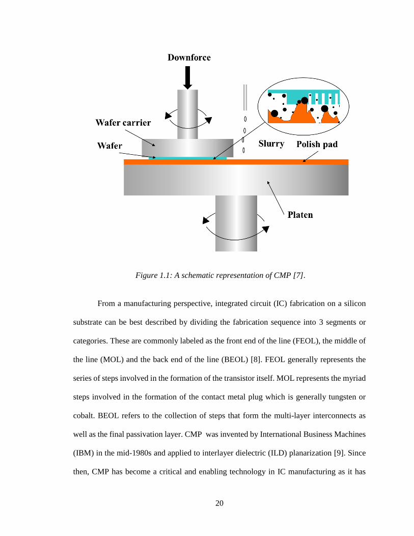
20
Figure 1.1: A schematic representation of CMP [7].
From a manufacturing perspective, integrated circuit (IC) fabrication on a silicon
substrate can be best described by dividing the fabrication sequence into 3 segments or
categories. These are commonly labeled as the front end of the line (FEOL), the middle of
the line (MOL) and the back end of the line (BEOL) [8]. FEOL generally represents the
series of steps involved in the formation of the transistor itself. MOL represents the myriad
steps involved in the formation of the contact metal plug which is generally tungsten or
cobalt. BEOL refers to the collection of steps that form the multi-layer interconnects as
well as the final passivation layer. CMP was invented by International Business Machines
(IBM) in the mid-1980s and applied to interlayer dielectric (ILD) planarization [9]. Since
then, CMP has become a critical and enabling technology in IC manufacturing as it has

21
brought about many benefits such as: (a) improved photolithography and dry etch yields;
(b) excellent conformality and step coverage; (c) minimal wafer-level defects; (d) minimal
line shorts and minimal undesired contacts and electro-migration effects; (e) reduced
contact resistance and inhomogeneous metallization layer thicknesses; and (f) improved
mechanical strength needed for stacking of multi-layer metal layers [3]. At the 0.8 μm
technology node, ILD CMP enabled complex multilayer metal interconnection in both
logic and memory devices [2]. Later on, the 0.35 μm technology node was developed with
the introduction of shallow trench isolation (STI) CMP [10] as well as polysilicon CMP
[11] in FEOL processes. The application of tungsten CMP in the MOL and BEOL
processes enabled manufacturing below the 0.18 μm node. Copper metallization
technology in BEOL (also known as dual-damascene) was then introduced to replace
aluminum interconnects which provided superior conductivity and chip manufacturability
[12, 13].
1.2. Applications of CMP
As mentioned above, applications of CMP in semiconductor manufacturing can be
found in all three segments (i.e. FEOL, MOL and BEOL) of the process flow as shown in
Figure 1.2 [1]. As the industry started moving towards more advanced technology nodes,
innovations such as fin formation and replacement metal gate (RMG) technology have
been introduced. These innovations resulted in dramatic increases in the number of CMP
steps in FEOL and MOL [8] such that, today, the total number of CMP processes in
advanced semiconductor manufacturing has increased to at least 25 steps (Figure 1.3). In
this section, we will briefly describe the STI, RMG, ILD and copper CMP steps.

22
Figure 1.2: CMP applications in advanced logic technology [8].
Figure 1.3: The increase in the number of CMP steps with technology nodes [8].

23
1.2.1. STI CMP
STI technology was first introduced at the 0.25 μm node as it gradually replaced
the traditional local oxidation of silicon (LOCOS) structures to provide dielectric isolation
between transistors [14]. The flow of the STI process starts with a thin thermal silicon
dioxide growth process followed by silicon nitride deposition. Both layers in the isolation
area are then etched (via reactive ion etching) to form the trench. Thereafter, using chemical
vapor deposition (CVD), silicon dioxide is deposited over the trench [8, 15-18]. After the
CVD step, STI CMP is used to completely remove excess silicon dioxide present on top of
the active area. This CMP step is preferred to stop on the silicon nitride layer and not
planarize any further [3, 19]. At the end, the silicon nitride layer is stripped off by dry
etching and the active silicon region is exposed which allows the construction of the
transistor gate.
There are two steps involved in STI CMP. The first step is to planarize the bulk
silicon dioxide overhang down to a thickness of about 500 to 1000 Å. In this step, silica-
based slurries, that are at a lower cost compared to more advanced slurries, are typically
used and polishing downforce is generally maximized to ensure high removal rates. The
performance requirement for the first polishing step is to achieve good global planarity of
the remaining silicon dioxide film with minimal number of surface defects (i.e. scratches).
A second CMP step is then used to remove the remaining silicon dioxide film and expose
the active silicon nitride layer with minimal loss of the silicon nitride as well as minimal
dishing of the silicon dioxide layer present in the trench. The removal rate selectivity of
the silicon dioxide layer compared to the silicon nitride layer is very important in reducing

24
over-polishing or silicon nitride erosion in this step. As such, high silicon dioxide removal
rate needs to be maintained while the silicon nitride removal rate needs to be minimized in
the second STI CMP step.
Figure 1.4: A schematic representation of the STI process. Note that the dielectric
material denoted by “D” may be pure or other forms of SiO2 [20].

25
To accomplish this, ceria slurries are commonly selected because of their inherently
high silicon dioxide removal rates and outstanding selectivity against silicon nitride [8].
The key performance metric of the second STI CMP step is the complete removal of all
the silicon dioxide material that is on top of the silicon nitride. Any remaining silicon
dioxide film on the active silicon nitride areas will act as a mask during silicon nitride
stripping which can lead to incomplete silicon nitride striping. This will cause the transistor
to fail [21, 22]. Furthermore, non-uniform silicon nitride loss will result in a non-uniform
step height between the silicon dioxide and the active silicon region. Any non-uniform step
height generated in the STI region can cause a non-uniform transistor gate level, which will
lead to incomplete contact on the gate at the MOL segment of the process [8].
1.2.2. RMG CMP
Replacement metal gate (RMG) CMP is a relatively new application. High-k metal
gate (HKMG) integration using an RMG approach was initially developed by Intel and
implemented in the 45nm technology node in 2007 [23]. Figure 1.5 shows the schematic
of the RMG technique. The dummy polysilicon gate is first created before the growth of
the real metal gate. Then, silicon nitride and contact etch stop layers are deposited. The
dielectric that is deposited on the top of the silicon nitride film is removed by CMP until
the silicon nitride film on the top of the dummy gate is exposed. After this step, the dummy
poly gate is etched out and a blanket gate trench is formed. Metal gate (i.e. aluminum or
tungsten electrodes) is deposited last [8, 24-26]. As shown in Figure 1.5, RMG technology
involves two steps: (1) Poly opening CMP (POC) before dummy polysilicon etching, and
(2) Metal gate CMP after metal deposition [1].

26
Figure 1.5: A schematic of RMG CMP [23].

27
The goal of the first POC process is to remove the dielectric and expose the silicon
nitride film. The critical performance requirement here is to minimize silicon nitride loss.
Therefore, a slurry with high removal rate selectivity on silicon dioxide over silicon nitride
is necessary. The typical silicon dioxide-to-silicon nitride removal rate selectivity,
expressed in terms of a ratio, that is required in the POC process is more than 50:1 [8]. In
the second metal gate CMP step, the process margin is critical in overcoming the
topography created during the first POC process. Any excessive over-polishing in either
step can cause thin gates with high gate resistance [27]. Other major concerns for RMG
CMP are metal dishing and erosion, metal gate height uniformity control and wafer-level
defects [23]. Generally speaking, these two RMG CMP steps have very narrow process
margins. As such, an extremely precise process control is necessary in order to have high
yields. Since the dimension of the gate is very small, the yield of the metal gate device
highly depends on CMP-induced defects [27, 28].
1.2.3. ILD CMP
ILD CMP is the most conventional CMP process in semiconductor manufacturing.
A schematic of ILD CMP that isolates the FEOL transistor region from BEOL
metallization is shown in Figure 1.6. In MOL and BEOL, the major goal of ILD CMP is
to provide a planar surface between the increasing numbers of metal layers. After ILD
CMP, the planarized dielectric surface is etched out to create the metal trench as well as
the via. The via is then filled with the metal layer, which is planarized by a subsequent
metal CMP step. ILD CMP should stop with accurate final target thickness of the dielectric
and the surface finish should be nearly defect-free with the required film thickness non-

28
uniformity. Any defects remaining on the surface will cause an incomplete etching during
the following steps. Therefore, the major development work in ILD CMP has focused on
the improvement of consistent material removal rate and uniformity.
Figure 1.6: A schematic of ILD CMP.
1.2.4. Copper CMP
Copper interconnects were first introduced to IC manufacturing in 1997 due to
copper’s lower resistivity, and became the industry standard soon thereafter. Copper CMP
continues to be a rapidly growing segment in modern semiconductor device manufacturing

29
[29, 30]. In the dual damascene process, trenches in the ILD layer are created through
etching. Then, a TaN/Ta barrier layer is deposited by means of physical vapor deposition
(PVD). The barrier layer plays an important role in promoting film adhesion as well as
preventing the diffusion of copper and oxygen, therefore, enhancing the mechanical and
electrical reliability of the interconnect structure. Later, the PVD TaN/Ta barrier
technology was replaced by CVD cobalt or ruthenium liners as the technology node
migrated to 22 nm [31]. Subsequently, copper is filled into the trenches by electroplating
[32, 33]. The excessive copper is then removed by CMP, which typically involves two
steps as shown in Figure 1.7. The first step is the removal of bulk copper with a hard stop
on the barrier layer. The second step is the removal of the exposed barrier layer without
causing any significant copper dishing or dielectric erosion.
The shrinking of the technology node and the innovations in materials bring many
challenges to copper CMP [8]. An example is the introduction of the new low-k dielectric
materials which tend to be highly porous with low mechanical strength. Therefore,
mechanical damage is easily created in low-k dielectric materials during copper CMP. In
order to reduce wafer-level defects and dielectric film collapse and delamination, precise
polishing process design and control are critical. Generally, copper CMP performance
metrics include removal rates, removal selectivity to the barrier, global and local planarity,
surface topography, dishing and erosion, and wafer-level defects [1].

30
Figure 1.7: A schematic of copper CMP [34].
1.3. Cost of Ownership and the Environmental Impact of CMP
CMP is one of the most expensive modules in today’s semiconductor
manufacturing due to its high cost of ownership (CoO) and relatively low polisher
throughput and tool availability. Consumables generally include slurry, pad, conditioning
disc, post-CMP cleaning solution, retaining ring and PVA brush. Presently, the slurry and
the pad comprise about 49 and 33 percent of the total consumables CoO, respectively, with

31
the conditioning disc coming in at 9 percent [35]. As such, slurry use reduction continues
to be the primary goal for IC manufactures who strive to reduce CoO. Similar to other
semiconductor manufacturing processes, Environmental Health and Safety (EHS)
concerns are also critical in the CMP module. Off-the-shelf slurries often contain hazardous
nano-particles and chemicalsSpent slurries also contain heavy metal such as copper,
tungsten, indium, arsenic and gallium which, if not treated properly, can pollute waterways,
harm human and animal life and damage the environment. Post-CMP cleaning solutions
often contain tetramethylammonium hydroxide (TMAH) which is classified as a toxic
material [36]. Therefore, optimizing the CMP process and reducing consumables usage
will always positively impact EHS.
Over the past 16 years, it has been a focal point of our research team to perform
fundamental studies in an effort to develop novel CMP materials, equipment and process
that reduce the EHS impact of the CMP module in IC manufacturing. As detailed below,
the motivation and goals of this study is also in line with the overall EHS goals of our field
of research.
1.4. Research Motivations and Goals
The primary motivation of this dissertation is to understand several fundamental
aspects of CMP and apply the findings to develop novel, EHS-friendly CMP processes. In
this dissertation we report on five independent, yet overall cohesive, studies. The
motivations and the goals of each study are described below:

32
• Method for Ultra-Rapid Determination of the Lubrication Mechanism in CMP
(Chapter 4): In CMP, Stribeck curves are normally constructed by plotting average
COF against the average Sommerfeld number. Consequently, traditional Stribeck
curves fail to provide a full explanation of the lubrication phenomena simply
because COF and polishing downforce can fluctuate significantly due to the
inherent stick-slip phenomena and the transient instabilities caused by polishing
kinematics and consumables. This study introduces a new method for rapidly
generating an “improved” Stribeck curve (which we have coined as the Stribeck+
curve) that shows a more complete tribological picture of the process. The method
significantly reduces the consumables and time required to obtain the curve
compared to traditional means. Results of the Stribeck+ curve are consistent with
individual tests using several different consumables combinations. All copper CMP
Stribeck+ examples clearly indicate the lubrication mechanism and transitions
thereof between different polishing conditions. Variability in COF as well as a
much wider range in U/P are also explored.
• Application of the Stribeck+ Curve in Silicon Dioxide CMP (Chapter 5): The
Stribeck+ curve is successfully applied to silicon dioxide CMP to characterize the
tribology of such processes under different process conditions and consumables.
Results show that the Stribeck+ curve is capable of rapidly determining and
differentiating the tribological mechanism among all cases studied in this
manuscript. The Stribeck+ curve is also shown to be a measure of process stability
as seen by the spread of the COF vertical clusters. The Stribeck+ curve also

33
confirms a previously known effect that the greater the ratio of the up-features of
the pad to the total pad area, the greater the probability of wafer hydroplaning. This
work underscores the importance of a new method for determining an “improved”
Stribeck curve while dramatically reducing the amount of consumables and time
required to obtain the curve through traditional means.
• Effect of Pad Surface Micro-Texture on Tribological, Thermal and Kinetic
Characterizations during Copper CMP (Chapter 6): During CMP, a polishing pad
directly contacts the wafer and transports the slurry into the wafer-pad interface.
The micro-texture (i.e. the combination of asperity heights, densities and radii of
curvature) of the polishing pad plays an important role in holding the slurry which
could then affect removal rate, uniformity and wafer-level defect counts. The
objective of this study is to investigate the effect of pad surface micro-texture on
the tribological, thermal and kinetic attributes in copper CMP. Two substantially
different CVD conditioning discs are employed to generate and study two different
pad surface micro-textures (i.e. contact area, pad surface height probability density
function and pad surface abruptness). For each disc, several 300-mm copper wafers
are polished and then removal rate, COF and pad surface temperature are measured.
Pad surface micro-texture in terms of pad contact area and topography are analyzed
via a laser confocal microscopy. The modified two-step Langmuir-Hinshelwood
removal model is used to simulate removal rate along with chemical and
mechanical rate constants, and to improve the understanding of chemical and
mechanical aspects of the process and help optimize polishing conditions.

34
• Effect of Various Slurry Injection System Configurations on Removal Rates of
Silicon Dioxide Using a Ceria-Based CMP Slurry (Chapter 7): Conventional
center-point application methods lead to low slurry utilization efficiency and poor
performance. To reduce slurry usage while maintaining an acceptable process
performance (i.e. removal rate, selectivity, planarity and wafer-level defects), a
novel slurry injection system (SIS) has been introduced and continuously improved
upon. In the STI process, in certain ceria slurry formulations, addition of water acts
to reduce removal rate (what the industry calls “direct slurries”) while with certain
other formulations (“reverse slurries”) adding water promotes material removal.
Our study here aims to optimize the position of the SIS on the polisher in order to
obtain a more cost-effective and environmentally benign CMP process using a
widely-adopted ceria based “reverse slurry”. Here, we configure the SIS at various
angles (or orientations) in order to investigate slurry dilution characteristics that
affect silicon dioxide removal rates. UPW dilution effect on removal rate, COF and
pad surface temperature, caused by residual rinsing, is also explained by
maintaining a constant dilution ratio for each of the SIS configuration tests. That
way, any mixing and dilution effects can be attributed to, and explained by,
differences in the position of the SIS only. Removal rate as a function of slurry flow
rate and polishing time is also studied to provide a better understanding of water
dilution effects over time. Finally, silicon dioxide to silicon nitride removal rate
selectivity tests are done to ensure proper final recommendations.

35
• Effect of Conditioning and Slurry Application Method on Silicon Dioxide Removal
Rates Using a Ceria-Based CMP (Chapter 8): In CMP, conditioning is done in in-
situ (i.e. conditioning while polishing) or ex-situ (i.e. conditioning before polishing)
modes. The constant sweeping of the conditioner may change the slurry flow
pattern and the amount and location of the residual rinse water, the impacts of
conditioning will be amplified when a “reverse” slurry is used. Our study aims to
investigate silicon dioxide removal rate with a “reverse” ceria slurry when four
different combinations of conditioning and slurry application methods are used.
These various combinations will be discussed in detail in the experimental section.
The frictional analysis and Stribeck+ curves are employed to fundamentally
elucidate the impact of the conditioning method on the tribological characteristics.
The systematic study of slurry, conditioning and removal rate is explored with
respect to COF fluctuations and stick-slip phenomena. Finally, the removal rate is
correlated to the extent of process vibration which helps provide a better
understanding of “reverse” ceria slurry removal characteristics.
1.5. Explanation of Dissertation Format
This dissertation has been prepared in accordance with the format prescribed by the
University of Arizona Graduate College Manual for Electronic Theses and Dissertation
and is consistent with the formatting requirements of the Department of Chemical and
Environmental Engineering. This work consists of 9 chapters including 5 manuscripts
(each presented in the dissertation as a separate chapter). The contributions to each
manuscript are summarized below.

36
Chapter 4. Method for Ultra-Rapid Determination of the Lubrication Mechanism in
CMP
The experiments were performed by the author, Dr. Yasa Sampurno, Dr. Yun
Zhuang and Siannie Theng. Fransisca Sudargho developed the LabView software which
allowed the collection of data generated during the experiments. Experimental data
analyses were conducted by the author with help from Dr. Yasa Sampurno and Dr. Ara
Philipossian. The manuscript was written by the author and edited by Dr. Ara Philipossian
and Dr. Yasa Sampurno. Multiple correspondences with the archival journal editors that
resulted in the publication of the manuscript were led by the author.
Chapter 5. Application of the Stribeck+ Curve in Silicon Dioxide CMP
The experiments were performed by the author, Dr. Yasa Sampurno, Dr. Yun
Zhuang and Siannie Theng. Fransisca Sudargho developed the LabView software which
allowed the collection of data generated during the experiments. Experimental data
analyses were conducted by the author with helping from Dr. Yasa Sampurno and Dr. Ara
Philipossian. The manuscript was written by the author and edited by Dr. Ara Philipossian
and Dr. Yasa Sampurno. Multiple correspondences with the archival journal editors that
resulted in the publication of the manuscript were led by the author.
Chapter 6. Effect of Pad Surface Micro-Texture on Tribological, Thermal and
Kinetic Characterizations during Copper CMP
The experiments were performed by the author and Dr. Yan Mu. Experimental data
analyses were conducted by the author with help from Dr. Yasa Sampurno and Dr. Yun

37
Zhuang. The manuscript was written by the author and edited by Dr. Ara Philipossian and
Dr. Yasa Sampurno. Multiple correspondences with the archival journal editors that
resulted in the publication of the manuscript were led by the author.
Chapter 7. Effect of Various Slurry Injection System Configurations on Removal
Rates of Silicon Dioxide Using a Ceria-Based CMP Slurry
The experiments were performed by the author, Matthew Bahr and Morgan
Skillman with advice from Dr. Yasa Sampurno. The SIS was designed by Dr. Leonard
Borucki. Experimental data analyses were conducted by the author with help from Dr. Yasa
Sampurno. The manuscript was written by the author and edited by Dr. Ara Philipossian
and Dr. Yasa Sampurno. Multiple correspondences with the archival journal editors that
resulted in the publication of the manuscript were led by the author.
Chapter 8. Effect of Conditioning and Slurry Application Method on Silicon Dioxide
Removal Rates Using a Ceria-Based CMP Slurry
The experiments were performed by the author and Matthew Bahr with advice from
Dr. Yasa Sampurno. The SIS was designed by Dr. Leonard Borucki. Experimental data
analyses were conducted by the author with help from Dr. Yasa Sampurno. The manuscript
was written by the author and edited by Dr. Ara Philipossian and Dr. Yasa Sampurno.
Multiple correspondences with the archival journal editors that resulted in the publication
of the manuscript were led by the author.

38
Chapter 2. Experimental Apparati

39
2.1. APD-800 Polisher and Tribometer
The Araca APD-800 is a single-platen polisher and tribometer designed specifically
for 200 and 300 mm wafer CMP applications. The polisher can also accurately measure
shear force and downforce in real-time during polishing. Shear force data are acquired and
analyzed to elucidate the tribological characteristics of a given CMP process. The main
hardware components of the APD-800 are shown in Figure 2.1 and their functions are
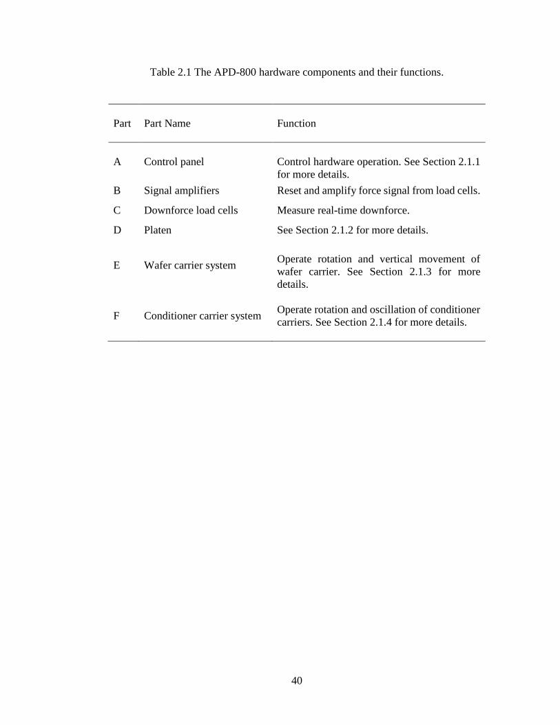
listed in Table 2.1.
Figure 2.1: The APD-800 polisher and tribometer.
40
Table 2.1 The APD-800 hardware components and their functions.
Part Part Name
Function
A Control panel
Control hardware operation. See Section 2.1.1
for more details.
B Signal amplifiers Reset and amplify force signal from load cells.
C Downforce load cells Measure real-time downforce.
D Platen See Section 2.1.2 for more details.
E Wafer carrier system
Operate rotation and vertical movement of
wafer carrier. See Section 2.1.3 for more
details.
F Conditioner carrier system
Operate rotation and oscillation of conditioner
carriers. See Section 2.1.4 for more details.

41
2.1.1. Control Panel
Figure 2.2 shows the APD-800 front panel. Components and their functions are
listed in Table 2.2.
Figure 2.2: The front panel of the APD-800.

42
Table 2.2 Components and functions of the APD-800 front panel.
Part Component
Function
A
Control panel
Control hardware operation.
B ON switch Turn on APD-800.
C OFF switch Turn off APD-800.
D Emergency stop switch
Stop polisher operations immediately in case of
emergency.
E Auto run STOP switch
Stop polishing sequence for automatic run set-
up; reset tool after alarm deactivation.
F Auto run START switch
Start polishing sequence for automatic run set-
up.
G Manual/auto run switch
Switch run mode between “Manual” and “Auto”.
H Shear force conditioner and
amplifier
Reset and amplify shear force signal from load
cell.
I USB connector
Connect APD-800 to the PC for data acquisition.
J Downforce conditioner and
amplifier
Reset and amplify downforce signal from load
cell.
2.1.2. Polishing Platen System and Downforce Measurement
The polishing platen (Figure 2.3) provides two basic functions: First, it serves as a
base for installing the polishing pad, and second, it rotates the pad counter-clockwise
during wafer polishing. The platen surface is made of ceramic, which is chosen to minimize
corrosion from the chemicals in the slurry. To measure the actual downforce during

43
polishing, four load cells are installed at the bottom of the platen assembly (one at each
corner as shown in Figure 2.3). The downforce is reported as the summation of forces from
those four load cells through a proprietary algorithm.
Figure 2.3: The polishing platen system of the APD-800.
2.1.3. Wafer Carrier System and Shear Force Measurement
The wafer carrier system exerts an exact amount of downforce to the backside of
wafer against the pad. Figure 2.4 shows the wafer carrier system of the APD-800. It
consists of vacuum pressure lines, carrier head motor, pressure chamber, and carrier head.
There are two separate vacuum-pressure lines installed inside the wafer carrier system. One
line is used to apply pressure to the carrier head, which applies downforce to the wafer
during polishing. The other line is to provide vacuum to hold the polycarbonate wafer

44
template attached to the carrier head. The template is equipped with a retaining ring and
backing film assembly. The retaining ring prevents the wafer from slipping out while the
wetted backing film assembly is used to securely hold the wafer via capillary forces.
Figure 2.4: Wafer carrier system of the APD-800.
To measure the shear force between the wafer and the pad, a sliding table is
employed in the wafer carrier system. The sliding table (Figure 2.5) consists of a bottom
plate held stationary by its attachment to the polisher frame, and an upper plate is movable.
During polishing, the upper plate slides with respect to the bottom plate in only one
direction (i.e. the y direction). Therefore, the shear force is reported by the Fy load cell.

45
Figure 2.5: Shear force measurement system of the APD-800.
During polishing, the load cell converts the frictional force into a voltage signal.
The voltage signal is then transmitted to the data acquisition system. Figure 2.6 shows the
shear force and the downforce measured during polishing. In the figure, the red curve
represents the shear force and the green curve represents the downforce, respectively.

46
Figure 2.6: An example of shear force (red curve) and downforce (green curve)
measurement.
2.1.4. Pad Conditioning System
Pad conditioning in CMP is aimed to maintain pad surface micro-texture and a
consistent polishing performance. As shown in Figure 2.7, in the APD-800, the rotary
motor and the hydraulic piston are designed for the rotation and vertical movement of the
conditioner, respectively. In addition, a pressure line is used to apply pressure to the
conditioner through the pressure chamber. During conditioning, the pad conditioner
sweeps over the pad across its radius. The sweep schedule can be divided into 10 different
zones with programmable lengths that way disc dwell time can be customized by the user
for each zone to ensure proper and even contact with the pad.

47
Figure 2.7: The pad conditioning system of the APD-800.
2.1.5. Data Acquisition Program
The data acquisition program for the APD-800 is written in LabView®. Figure 2.8
shows one of the panels to which the operator may access. During polishing, shear force,
downforce, pad temperature, slurry flow rate, platen/wafer/conditioner rotation rates,
conditioner position and oscillation, as well as motor current are recorded.
.

48
Figure 2.8: Data acquisition program for APD-800.
2.1.6. Tool Specifications
The APD-800 and major component specifications are listed in Table 2.3.
Table 2.3 The APD-800 component specifications (APD-800 operations manual).
Description
Manufacturers Fujikoshi Machinery Corporation and Araca
Incorporated
Wafer Size 300-mm (or smaller)
Wafer Carrier
Downforce control = Pneumatic
Pressure = 0.6 to 8.0 PSI (1.4 to 8.0 PSI for 200-mm)
Rotation rate = 15 to 200 RPM
Platen
Φ = 800 mm
Rotation rate = 20 to 180 RPM
Material = SUS410
Built-in heat exchanger (requires external coolant)

49
Conditioner
Φ = 108 mm
Rotation rate = 12 to 120 RPM
Stroke length = 320 mm
Sweep velocity = 0 to 500 mm/s through ten
independently controlled zones
Downforce = 3.3 to 13.2 lb
Scheme = ex-situ or in-situ
Chemical Delivery Systems
Three computer-controlled, 20-liter, chemical-resistant,
removable tanks with impeller mixers, roller pumps and
level sensors.
Flow rate = 10 to 450 ml/min
Pad Water Rinse Deliciated high flow rate water rinse injector
Flow rate up to 3,000 ml/min
Force Sensors Shear force (1 sensor) and downforce (4 multiplexed
sensors)
Temperature Sensor Adjustable single-point pad surface IR detector
Data Capture vs. Time
(capture frequency up to
2,300 Hz; display frequency
= 1 Hz)
Platen rotational velocity
Carrier rotational velocity
Conditioner rotational velocity, position, oscillation
speed and motor current
Tanks 1, 2 and 3 chemical flow rates
Shear force and downforce
Coefficient of friction (COF)
Pad surface temperature
Basic Data Analysis Average and variance of the entire (or subset of the)
polishing period for all parameters being captured
Advanced Data Analysis and
Correlation
Shear force and downforce Fast Fourier Transform
(FFT)
COF vs. Sommerfeld number
COF vs. pad temperature
Control, Monitoring and
Analysis
Programmable touch-screen controller for polisher
operation
Notebook computer for process monitoring and data
analysis
Width × Length × Height
100 × 140 × 203 cm (polisher)
80 × 38 × 190 cm (electrical cabinet)
50 × 150 × 81 cm (three chemical delivery systems)
CDA Minimum pressure = 72 PSI (500,000 Pa)
Flow rate = 550 liter per minute
Platen Coolant Water Maximum pressure = 43 PSI (300,000 Pa)
Flow rate = 15 liters per minute

50
2.2. Laser Scanning Confocal Microscopy
Confocal microscopy is an imaging technique that allows spatial filtering to
exclusively collect the light from a single focal plane in specimen. Confocal microscopy is
capable of scanning through the specimen to construct the combined 3D image. Confocal
microscopy offers many advantages over conventional optical microscopy such as
adjustable depth of field (DOF), the elimination of image information of the out-of-focus
plane, and the ability to collect stack optical slides from the specimen. As a result, the
popularity of confocal microscopy has increased tremendously when it comes to research
in the fields of life sciences, semiconductor industry and material sciences [37]. In Chapter
6, the pad surface micro-texture (i.e. contact area and pad topography) will be analyzed
using a Zeiss LSM 510 META laser confocal microscopy (shown in Figure 2.9).
Figure 2.9: Zeiss LSM 510 META laser confocal microscopy [38].
51
2.2.1. Confocal Microscopy Working Principles
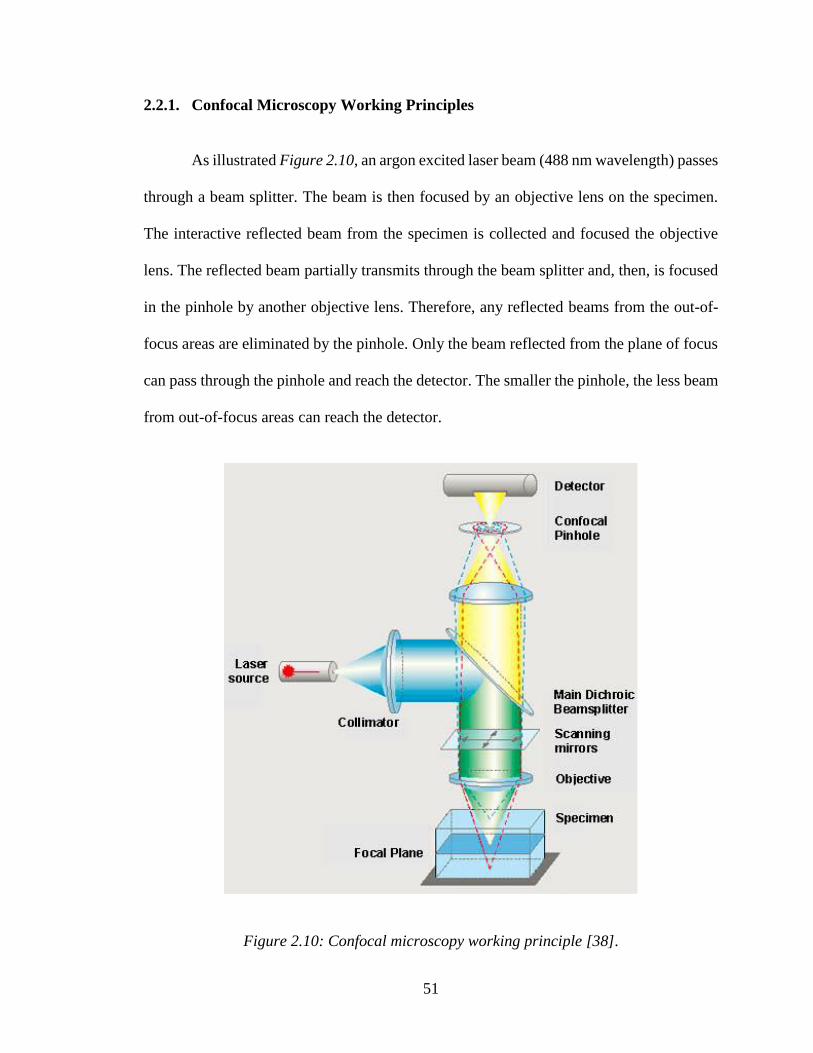
As illustrated Figure 2.10, an argon excited laser beam (488 nm wavelength) passes
through a beam splitter. The beam is then focused by an objective lens on the specimen.
The interactive reflected beam from the specimen is collected and focused the objective
lens. The reflected beam partially transmits through the beam splitter and, then, is focused
in the pinhole by another objective lens. Therefore, any reflected beams from the out-of-
focus areas are eliminated by the pinhole. Only the beam reflected from the plane of focus
can pass through the pinhole and reach the detector. The smaller the pinhole, the less beam
from out-of-focus areas can reach the detector.
Figure 2.10: Confocal microscopy working principle [38].

52
A photomultiplier tube (PMT) detects the light intensity and transforms the optical
signals into electrical signals which are then analyzed by a computer. The laser beam scans
the specimens by moving the scanning mirrors in x and y directions so that the detector
builds up the 2D image pixel by pixel. Raising and lowering objective lens, the laser beam
can scan another plane of interest. Based on the stack of 2D image, a high-resolution 3D
image is finally achieved [39, 40].
In this dissertation, a custom-made pad sample holder (designed and constructed
by our research group) with a sapphire window will be used to measure the contact
information between pad-wafer interface. The sapphire window works as a “wafer” to
simulate the pad-wafer because the sapphire material is transparent and has an index of
refraction similar to that of polyurethane (i.e. the pad material) [41]. The top surface of the
pad specimen is placed against the sapphire window and different known pressures are
applied to the sapphire-pad stack to simulate pressures encountered during actual polishing.
The pad sample is illuminated by the laser source through a high-numerical-aperture
objective. The reflected light from the sample will be projected onto an optically conjugate
situated pinhole. Figure 2.11 illustrates the light reflection and refraction path at the
sapphire window-pad interface. According to the Snell’s Law [42], at the contact points,
light incident on a contact region is therefore not reflected back. Such a setup ensures that
only in-focus reflected lights are detected by detector.

53
Figure 2.11: Illustration of light reflection and refraction at the pad-wafer interface [43].
2.2.2. Contact Area Analysis
Figure 2.12 shows an example of a reflected image collected at the pad-wafer
contact region using the confocal microscopy. The areas with an even gray color are located
substantially below the sapphire interface. Contact areas are represented by black spots.
Constructive and destructive interferences in the near-contact areas produce “zebra stripes”
which are associated with relatively flat areas of the pad. Based on Liao’s work [44], solid
contact areas correspond to clear pore structures and large flat near-contact areas
correspond to fractured and collapsed pore walls. Based on the contact image, contact area
percentage is then calculated by dividing the measured contact area over the total analyzed
pad surface area.

54
Figure 2.12: An example of a reflection image collected at the pad-wafer contact region using
the laser confocal microscopy.
2.2.3. Topography Analysis
Figure 2.13 shows an example of pad topographic images collected by the laser
confocal microscopy. In the topographic image, the blue color areas refer to relatively
lower levels of the pad surface thus corresponding to the pore structure of the pad, while
the red color areas refer to relatively higher levels of the pad surface which correspond to
pad asperities.
Based on the high-resolution pad surface topography images, the pad surface height
probability density function can be established for each disc as shown in Figure 2.14. The
right side of the curve (𝑧 > 0 µ𝑚) corresponds to the upper part of pad surface including
pad asperities that contact the wafer during polishing.

55
Figure 2.13: An example of topography image using the laser confocal microscopy.
Figure 2.14: Example of a plot of pad surface height probability density function (PDF).
When the asperity summits have exponentially distributed heights, the right-hand
tail of the curve will be linear on a logarithmic plot, and can be characterized by a decay
56
length which is designated as 𝜆. This (i.e. 𝜆) is referred to as pad surface abruptness and
defined as the distance over which the right-hand tail of the surface height probability
density drops by a factor of 𝑒. Detailed descriptions of the abruptness analysis can be found
elsewhere [43, 45]. Generally speaking, a pad surface having a higher value of 𝜆 indicates
a larger range of surface heights and, therefore, the surface appears to be less smooth. When
𝜆 is small, there is a small range of surface heights and the surface is considered to be
somewhat smooth. Chapter 6 will describe how the confocal analysis results related to the
polishing performance.
2.3. Film Thickness Analytical Tools
In this dissertation, wafer film thickness is measured on multiple points on the
surface before and after the polishing to determine the material removal rate. Thickness of
metal film and non-conductive film is measured by an Advanced Instrument Technology
(AIT) CMT-SR5000 sheet resistance measurement system and a SENTECH Film
Thickness Probe (FTP) reflectometer, respectively.
2.3.1. Reflectometer
FTP reflectometer (Figure 2.15) is able to measure the spectral reflectance of
substrates, single films and layer stacks. A light beam with certain wavelength
perpendicular to the thin film is used as source. The reflected light beam from the bottom
and the top interfaces of the thin film will interfere either constructively or destructively
due to the phase shift. As such, a unique reflectance spectrum is formed. The reflectance
spectrum is a function of the film thickness, refractive index and extinction coefficient of

57
the film and the substrate. To determine film thickness, the software generates a predicated
reflectance spectrum by fitting the real measured spectrum. The optimized fitting results
(i.e. film thickness) will be reported until the predicted spectrum matches the measured one
in certain tolerance.
Figure 2.15: SENTECH FTP reflectometer.
2.3.2. Sheet Resistance Measurement System
The pre-and post-thickness of all monitor wafers with metal films will be measured
by the CMT-SR5000 tool as shown in Figure 2.16. The film thickness is determined by
measuring the sheet resistance:
𝑅𝑠 =𝛺
ℎ×
𝑙
𝑤 Equation 2.1
where 𝑅𝑠 is sheet resistance, 𝛺 is the electrical resistance of the measured film material, ℎ
is the metal film thickness, 𝑙 is the length of the cross-sectional area and 𝑤 is the width of

58
the cross-sectional area. For a square slab, 𝑙 = 𝑤 and then the metal film thickness can be
calculated. The sheet resistance of the thin film can be realized using “four-point probe”.
Figure 2.16: AIT CMT-SR5000 sheet resistance measurement system.
The schematic working principle of a four-point probe is shown in Figure 2.17. A
current is passed through the outside two probes and induces a voltage in the inner two
voltage probes. If the spacing between the probe points is constant, and the conducting film
thickness is less than 40% of the spacing, based on Maxwell’s field equations, the sheet
resistance is given by [46]:
𝑅𝑠 =𝜋
𝑙𝑛2
𝑉
𝐼= 4.53
𝑉
𝐼 Equation 2.2
Figure 2.17: Four-point probe sheet resistance measurement [46].

59
Chapter 3. General Theory

60
3.1. Silicon Dioxide Removal Mechanism
The process of hydrolysis of SiO2 is fundamental to silicon dioxide CMP. In the
past, most silicon dioxide removal mechanisms were proposed by studying glass polishing.
Silvernail et al. [47] indicated the necessity for the presence of water during glass polishing.
Later, Iler [48] proposed the reaction mechanism between water and the Si-O-Si structure
on the surface of SiO2. Izumitani [49] showed that soft hydrated SiO2 layers could be easily
removed by a slurry that contained abrasive particles. Tomozawa et al. [50] further studied
the formation of the hydrated SiO2 layer and identified the presence of a 100 Å thick
hydrated layer on the surface of SiO2. Based on the above mentioned studies, Cook
proceeded to develop what is now considered as a widely accepted and comprehensive
SiO2 removal mechanism [51]. In brief, Cook postulated the following: The hydrolysis
reaction first occurs on silicon dioxide surfaces to form surface silanol groups (Si-OH).
This is followed by the formation of Si(OH)4 which is caused by the dissolution of silica
[48]. Compared to the SiO2 film, Si(OH)4 is said to be more fragile, thus it can be easily
scrubbed off by the slurry abrasives particles that are stuck within the pad asperities, and
to some extent, by the pad asperities themselves. Cook further indicated that the hydrolysis
process is controlled by pH such that at pH values in excess of 9, there is a catalytic effect
on the formation of hydroxyl groups to boost the silicon dioxide removal rate. The reaction
that occurs is described as:
From the optical lens polishing technology, it is well known that silicon dioxide
can also be removed by using slurries that contain metal oxide abrasives such as cerium
(SiO2)x + 2H2O → (SiO2)x−1 + Si(OH)4 Equation 3.1
61
oxide, zirconium oxide, titanium oxide and thorium oxide. In STI CMP, slurries using
cerium dioxide (a.k.a. ceria) abrasive nanoparticles are gaining widespread acceptance due
to their superior removal rate when it comes to silicon dioxide as compared to silicon
nitride [52-54]. In layman’s terms, this is referred to oxide-to-nitride removal rate
selectivity. Cook [51] indicated that most metal oxide based abrasives possess a great
affinity for the SiO2, which helps in SiO2 bond breaking. When water exists, the surface of
SiO2 is mostly terminated with -Si-OH group. According to Cook’s mechanism [51], the
active -Si-O- sites on the SiO2 surface react with the Ce-OH (from the cerium oxide
abrasive) to form Ce-O-Si bonds and subsequently release Si(OH)4 into the solution. The
proposed reaction is:
−Ce − OH + Si − O− ↔ −Si − O − Ce− + OH− Equation 3.2
Since the Ce-O-Si structure is stronger than the Si-O-Si structure, SiO2 is removed by both
chemical and mechanical actions (Figure 3.1a) [51]. This suggests that SiO2 is removed
one molecule at a time, in the form of Si(OH)4.
A similar removal mechanism by Kelsall [55] suggested that the Ce3+ on the surface
of ceria abrasives reacts with the hydrated silicon dioxide surface. Sabia and Stevens [56]
proposed that the removal of silicon dioxide is due to the reaction between the ceria
abrasives and the wafer surface, promoted by the presence of Ce3+ on the abrasive surface.
Later, Hoshino et al. [57], proposed a different model that silicon dioxide is removed in
the form of lumps (Figure 3.1b) rather than in the form of single molecules of Si(OH)4 as
proposed by Cook [51]. Their results were supported by analyzing the spent slurry
(containing the removed material) using Fourier transform infra-red spectroscopy and

62
inductively coupled plasma atomic emission spectroscopy. In another study, Veera Dandu
et al. [58] indicated that Ce3+ (and not Ce4+) present on the ceria abrasives improves the
removal of silicon dioxide (Figure 3.1c). This hypothesis was supported by UV-visible
spectroscopy data as well as thermogravimetric analysis. Results showed that the blocking
of the active Ce3+ surface sites by the additives caused the reduction of silicon dioxide
removal rate.
Figure 3.1: Illustration of the interaction between ceria and silicon dioxide during
polishing: (a) model proposed by Cook [51]; (b) model proposed by Hoshino et al. [57];
(c) model proposed by Srinivasan et al. [20] in which Ce3+ species stabilized by an
oxygen vacancy are the active species.

63
3.2. Silicon Nitride Removal Mechanism
The hardness of silicon nitride is higher than that of silica and ceria abrasive nano-
particles. In the presence of water, air or simply moisture, the silicon nitride surface can be
easily oxidized forming silicon dioxide species [59]. The overall oxidation reactions can
be written as:
Si3N4 + 3O2 → 3SiO2 + 2N2 Equation 3.3
Si3N4 + 6H2O → 3SiO2 + 4NH3 Equation 3.4
In silicon nitride CMP, the silicon nitride layer is not removed directly. Rather, its
uppermost layer, which, as described below, are some sort of a chemically modified silicon
dioxide film, are removed. Hu et al. [60] proposed a sequence of hydrolysis reactions that
convert the silicon nitride surface to Si-O-Si structures and NH3 (dissolved in ammonia in
form of NH4OH). The chemically modified silicon nitride surface layer may be further
hydrated in the presence of water as shown in Equation 3.5. Si(OH)4 is then removed by
mechanical scrubbing [60].
≡ Si − O − Si ≡ + H2O → Si(OH)4 Equation 3.5
When the oxidation of silicon nitride is inhibited, the nitride removal may be
suppressed. In such a condition, mechanical removal due to slurry abrasive nano-particles
or pad asperities should be limited, since ceria abrasives are softer than the silicon nitride
film. Indeed, proline and other amino acids, when added to ceria slurries, can preferentially
adsorb on the surface of the silicon nitride preventing its oxidation to form silicon dioxide.
As such, the suppress the rate of silicon nitride removal [61].

64
3.3. Copper Removal Mechanism
The fundamental mechanism of copper CMP is based on the sequential oxidation
and dissolution of copper. Copper reacts in oxidizer-containing environments to form a
weak oxide layer that has a structure consisting of Cu2O and CuO/Cu(OH)2 [62]:
2Cu + H2O → Cu2O + 2H+ + 2e− Equation 3.6
Cu2O + H2O → 2CuO + 2H+ + 2𝑒− Equation 3.7
Cu2O + 3H2O → 2Cu(OH)2 + 2H+ + 2𝑒− Equation 3.8
Due to the presence of an inhibitor and a complexing agent, reactions occurring on the
copper surface can be quite complicated. Krishnan et al. indicated that Cu2O tends to
complex with benzotriazole (BTA) leading to the formation of a layer of CuI-BTA
molecules. Such a passivating layer can help prevent further corrosion of the Cu surface
[1]. Meanwhile, the water-soluble chelating agent (i.e. glycine) reacts with the free Cu2+
and/or Cu(OH)2/CuO to generate Cu2+-glycine complex [63]. Mechanical removal
mechanism also plays an important role in copper CMP. The pad and particles in the slurry
are capable of scrubbing the wafer surface. Nguyen et al. [64] indicated that the static etch
rate of copper is very low while copper removal rate is significantly higher during CMP.
Such results reinforce the theory that the passivation layer formed on the copper surface is
mostly removed by the abrasive nano-particles and the polishing pad.

65
3.4. Material Removal Models in CMP
3.4.1. Preston’s Equation
The Preston’s equation was first developed in 1927 for modelling glass polishing
[65]. In spite of it being decades old, Preston’s model has been widely used to correlate
removal rate to applied downward pressure and velocity in CMP:
𝑅𝑅 = 𝐾𝑝 × 𝑃 × 𝑈 Equation 3.9
Where 𝑅𝑅 is the material removal rate, 𝑃 is the polishing pressure, 𝑈 is the sliding velocity,
and 𝐾𝑝 is a coefficient that depends on the particular film being polished, as well as the
properties of the pad and the slurry. Although 𝐾𝑝 integrates within itself some of the
chemical contributions of CMP, the Preston’s equation is still mainly focused on
mechanical removal, with no direct inclusion of chemical effects. Therefore, Preston’s
equation is more accurate in cases where the chemical effect (or effects) of planarization is
(or are) relatively small (i.e. in ILD CMP applications). Figure 3.2 shows an example of
how removal rate is can be described using Preston’s equation for ILD CMP.

66
Figure 3.2: An example of application of the Preston model in ILD CMP [66].
3.4.2. Modified Preston’s Equation
Zhang et al. introduced an alternative removal model (Equation 3.10) by taking into
account both electrostatic particle adhesion and plastic deformation [67]. This model
considered the externally applied frictional force and the van der Waals forces between
slurry particles and the wafer surface responsible for material removal.
𝑅𝑅 = 𝐾 × (𝑃𝑈)1 2⁄ Equation 3.10
Since Preston’s equation is limited in cases where the chemical effect is strong (i.e.
copper CMP), the modified Preston’s equation as developed by Luo et al. [68] took on the
following form:

67
𝑅𝑅 = 𝐾𝑝𝑃𝑈 + 𝐵𝑈 + 𝑅𝑐 Equation 3.11
where 𝑅𝑐 and 𝐵 are constants. The term 𝐵𝑈 indicates a stronger velocity effect than the
pressure. The term Rc accounts for the chemical dissolution during polishing and depends
on the slurry composition [68].
3.4.3. Langmuir-Hinshelwood Removal Model
A far more fundamental model, the modified two-step Langmuir-Hinshelwood
model, has been successfully used to study the kinetic attributes of the CMP process. In
this model, an active reactant R in the slurry reacts with the film on the wafer surface (𝑀)
at a chemical react rate 𝑘1 to form a passivation layer L. For silicon dioxide or silicon
nitride CMP, R is simply water at a high pH value, while for copper or tungsten CMP, R
is, in most cases, water-diluted hydrogen peroxide.
𝑀 + 𝑅𝑘1→ 𝐿 Equation 3.12
This passivation layer L is then removed by pad scrubbing with a mechanical rate 𝑘2.
𝐿𝑘2→ 𝐿 Equation 3.13
Both of reactions can be assumed to pseudo 1st order reaction. Hence, the units of 𝑘1 and
𝑘2 are the same (will be discussed below). In this continuous process, the local removal
rate can be summarized as:
𝑅𝑅 =𝑀𝑤
𝜌
𝑘1𝑘2𝐶
𝑘2 + 𝑘1𝐶 Equation 3.14

68
where 𝑀𝑤 and ρ are the wafer surface material molecular weight and density, respectively.
𝐶 is the slurry reactant molar concentration. Since slurry utilization efficiency is very low,
𝐶 can be treated as a constant. Hence, 𝑘1𝐶 was renamed as 𝑘1 without loss of generality.
As such, 𝑘1 and 𝑘2 have the same units 𝑚𝑜𝑙/(𝑚2 ∙ 𝑠). The basic removal rate model hence
becomes:
𝑅𝑅 =𝑀𝑤
𝜌
𝑘1𝑘2
𝑘2 + 𝑘1 Equation 3.15
The chemical rate 𝑘1 can be calculated by Arrhenius equation:
𝑘1 = 𝐴exp(−𝐸
𝑘𝑏𝑇) Equation 3.16
where 𝐴 is an Arrhenius exponential factor and 𝐸 is the slurry activation energy of the rate-
limiting chemical step (i.e. the oxidation step in copper CMP). 𝐸 can be calculated by
plotting the natural log of the removal rate vs. the inverse of the mean pad temperature [45].
𝑘𝑏 is Boltzmann’s constant (i.e. 8.62×10⁻⁵ eV/K). 𝑇 is the wafer surface reaction
temperature which can be calculated by:
𝑇 = 𝑇𝑝 +𝛽
𝑈1 2⁄ +𝑒𝜇𝑘𝑃𝑈 Equation 3.17
where 𝑇𝑝 is the average pad temperature, 𝑈 is sliding velocity, 𝑃 is polishing pressure, 𝜇𝑘
is COF, 𝑒 and 𝛽 are fitting parameters. The mechanical rate 𝑘2 is proportional to the
frictional power density as suggested in Preston’s equation [65]:
𝑘2 = 𝑐𝑝𝜇𝑘𝑃𝑈 Equation 3.18

69
where 𝑐𝑝 is a proportionality constant.
It needs to be noted that ratio of simulated 𝑘1 to 𝑘2 (i.e. 𝑘1/𝑘2) is, at times, more
important than the individual value of 𝑘1 and 𝑘2 itself as the value of 𝑘1/𝑘2 can indicate
the controlling removal mechanism. In general, if the value of 𝑘1/𝑘2 is less than 1, the
polishing mechanism is, therefore, a chemically limited process. On the other hand, when
the value of 𝑘1/𝑘2 is greater than 1, the polishing process becomes mechanically limited.
3.5. Tribology in CMP
In a CMP system, surfaces of the wafer and the pad, together with the slurry
between them constitute a tribological system where two or more moving bodies come in
contact with one another, and as a result, begin to wear. Detailed tribological studies are
essential in understanding the fundamentals of CMP and in determining wear mechanisms
as well as end-of-life estimates for contacting bodies such as pads and diamond
conditioning discs.
3.5.1. Frictional Force and COF
A three-body interaction involving a wafer, a pad and slurry abrasive nano-particles
(Figure 3.3) results in two types of force: shear force (Fshear) and downforce (Fdown).
Consistent with the traditional definition of frictional force, the force from the down
pressure against the wafer is called downforce and the tangential force which applies shear
stress on the surface of the wafer is called shear force. Coefficient of friction (COF) is
defined as the ratio of the shear force (Fshear) to the downforce (Fdown) [69]:

70
COF = Fshear
Fdown Equation 3.19
COF is often related to the tribological attributes as well as material removal rates for CMP
processes [43, 44, 70, 71].
Figure 3.3: Schematic representation of three-body abrasions in CMP [72].
Accurate measurement of frictional force is a prerequisite to calculating COF and
therefore the understanding of the tribological phenomena during a CMP process. In this
dissertation, frictional force data are collected at a certain frequency (i.e. 1,000 Hz).
Therefore, the tribological attributes of a certain CMP process can be presented either by
the average or the instantaneous COF as a function of polish time. Average COF values
are calculated using Equation 3.20 where COFi refers to the instantaneous COF [73]:
COF̅̅ ̅̅ ̅ =1
n∑ COFi
n
i=1
Equation 3.20
In our system, the raw shear force data obtained as a function of time is separated
into two components [74]. One is the mean shear force of the system, 𝐹. The other one is

71
the fluctuating component of the mean shear force (i.e. variance of shear force), 𝑓(𝑡),
where,
𝐹(𝑡) = 𝐹 + 𝑓(𝑡) Equation 3.21
The fluctuating component 𝑓(𝑡) is mostly the result of stick-slip phenomena which
occur when pad asperities first get physically attached to the rotating wafer surface, and
only after the local shear force exceeds a certain amount, the asperities abruptly detach and
slip away from the wafer surface. Depending on the specific pad micro-texture (i.e.,
individual asperity height, density and radius of curvature), such phenomena can take place
at certain identifiable frequencies which can be analyzed from the raw shear force data [74,
75].
3.5.2. The Sommerfeld Number
The Sommerfeld number is dimensionless and it consists of a grouping of CMP
specific parameters described as [70]:
𝑆𝑜 =𝜇𝑈
𝑃𝑅𝑎 Equation 3.22
where 𝜇 is the slurry viscosity, 𝑈 is the pad-wafer relative sliding velocity, 𝑃 is the
polishing pressure from applied downforce against the pad, and 𝑅𝑎 is the pad surface
roughness. 𝑈 is determined by polisher platen diameter and relative angular velocity.
To determine the Sommerfeld number, each of the CMP specific parameters need
to be known. For a given slurry, 𝜇 is provided by the manufacturer or can be measured
through rheological experiments. Pressure 𝑃 is calculated by dividing the downforce

72
pressure by the wafer-pad contact area. Since pads with different groove designs may lead
to different land areas (i.e. wafer-pad contact area), the same applied downforce may result
in different polishing pressures. As a result, a dimensionless parameter 𝛼 which is equal to
the area of the up-features divided by the area of a flat pad, is introduced to accurately scale
the pressure for different pads [69].
3.5.3. Lubrication Mechanisms in CMP
Many researchers have studied the lubrication mechanism(s) in the pad-slurry-
wafer interface by experimentally obtaining the COF and constructing so called “Stribeck
curves” that show how COF changes with various groupings of CMP-relevant parameters
such as slurry viscosity, relative pad-wafer velocity, slurry film thickness and wafer
pressure [69, 76-79]. The most descriptive type of such Stribeck curves is the log-log plot
of the COF vs. the Sommerfeld number [80, 81] which has successfully provided
information on the extent of interactions among the wafer, pad and slurry abrasive particles
where three major lubrication mechanisms can be distinguished [69, 77-79].
Based on Ludema’s definition [82], there are three types of lubrication mechanisms
as depicted in Figure 3.4. In boundary lubrication, all solid bodies are in intimate contact
with each other. Boundary lubrication occurs at lower Sommerfeld numbers where the
Stribeck curve is relatively flat. Because of the intimate three-body contact presents in this
region, the values of COF are relative large. Partial lubrication mechanism typically
happens around intermediate values of the Sommerfeld number. Here, the three solid
bodies are not in intimate contact each other and the slurry film layer, with the same
thickness as the pad surface roughness, develops and partially separates the wafer and the

73
pad. As the lubrication mechanism transits from boundary lubrication to partial lubrication,
the slope of the Stribeck curve changes from a roughly flat line (i.e. almost zero) to a large
negative number (i.e. a rapidly decreasing line). Hydrodynamic lubrication occurs at larger
values of the Sommerfeld number, where smaller values of removal rate and COF are
typical. Here, a very thick slurry film in the wafer-pad interface often leads to wafer
hydroplaning during high sliding velocity CMP process.
Figure 3.4: The generic Stribeck curve based on the Sommerfeld number [82].
74
The study of Stribeck curve has also helped screen and identify certain consumables
by examining how they mechanically interact with each other which has ultimately led to
optimizing polishing parameters, increasing pad life and avoiding unstable polishing
conditions [69, 83]. In CMP, Stribeck curves have historically relied solely on the
determination of shear force and the subsequent calculation of the COF by dividing the
measured shear force (both mean and standard deviation) by the downforce. The latter has
always assumed to be constant and essentially calculated from the pressure set-point
programmed in the polisher’s micro-controller.
In Chapter 4, we will show that the traditional Stribeck curve fails to provide a full
explanation of the lubrication phenomena where fluctuations in the measured downforce
can indeed be dramatic and may be even more important than downforce values themselves.
Similarly, Stribeck curves provide no information about the relative standard deviation
(RSD) of COF. Fluctuations in COF are at times more important than their mean values.
Meanwhile, since the Sommerfeld number lumps 𝑈 (i.e. sliding velocity) and 𝑃 (i.e.
polishing pressure) together, it is often unclear as to which of these two parameters
contribute most to the tribological behavior. A new method for determining an “improved”
Stribeck curve (which here we refer to as the “Stribeck+ curve”) will be introduced.

75
Chapter 4. Method for Ultra-Rapid Determination of the Lubrication
Mechanism in CMP
P32 ECS Journal of Solid State Science and Technology, 6 (1) P32-P37 (2017)2162-8769/2017/6(1)/P32/6/$33.00 © The Electrochemical Society
Method for Ultra Rapid Determination of the LubricationMechanism in Chemical Mechanical PlanarizationRuochen Han,a,z Yasa Sampurno,a,b Siannie Theng,b Fransisca Sudargho,a,b Yun Zhuang,a,b
and Ara Philipossiana,b
aDepartment of Chemical and Environmental Engineering, University of Arizona, Tucson, Arizona 85721, USAbAraca, Inc., Tucson, Arizona 85718, USA
In chemical mechanical planarization (CMP), Stribeck curves are normally constructed by plotting average coefficient of frictions(COF) against the average Sommerfeld number. Consequently, traditional Stribeck curves fail to provide a full explanation of thelubrication phenomena simply because COF and polishing downforce can fluctuate significantly due to stick-slip phenomena andtransient instabilities caused by polishing kinematics and consumables. This study introduces a new method for rapidly generatingan “improved” Stribeck curve (i.e. Stribeck+ curve) that shows a more complete tribological picture of the process. The methodsignificantly reduces the consumables and time required to obtain the curve compared to traditional means. Results of the Stribeck+curve are consistent with individual tests using several different consumables combinations. All copper CMP Stribeck+ examplesclearly indicate the lubrication mechanism and transitions thereof between different polishing conditions. Variability in COF as wellas a much wider range in v/P are also explored.© 2016 The Electrochemical Society. [DOI: 10.1149/2.0111701jss] All rights reserved.
Manuscript submitted October 13, 2016; revised manuscript received November 28, 2016. Published December 16, 2016.
Chemical mechanical planarization (CMP) has proved to be criti-cal in achieving both local and global surface planarity during high-volume manufacturing of integrated circuits (IC). CMP significantlysimplifies the task of building multilayer IC devices while enablingunprecedented device yields and also meeting the ever stringent depthof focus requirements of photolithography.During CMP, a chemically rich slurry containing abrasive nanopar-
ticles is first delivered to the pad surface and allowed to form a thinfilm across the entire surface of the rotating polishing pad. A pat-terned wafer, having some gross topography, is then pressed facedown against the pad (which itself contains many surface asperitiesas well as deep grooves). Over time, a combination of chemical andmechanical effects removes the “up-features” on the wafer surfacethereby resulting in local and global planarization of the workpiece.During polishing, the pad surface wears down while its grooves assistin directing the spent slurry along with worn pad fragments (due to in-situ diamond disc conditioning of the pad) and reaction by-productsaway from the pad-slurry-wafer interface. This allows fresh slurry toenter the interface region and continue the polishing action.Based on the above simplified description, it becomes clear that
detailed tribological studies are essential in understanding the fun-damentals of CMP and in determining wear mechanisms as well asend-of-life estimates for contacting bodies such as pads and diamondconditioning discs. Many researchers have studied the lubricationmechanism(s) in the pad-slurry-wafer interface by experimentally ob-taining the coefficient of friction (COF) and constructing so called“Stribeck curves” that show how COF changes with various group-ings of CMP-relevant parameters such as slurry viscosity, relativepad-wafer velocity, slurry film thickness and wafer pressure.1–5 Themost descriptive type of such Stribeck curves is the log-log plot ofthe COF vs. the Sommerfeld number6–8 which has successfully pro-vided information on the extent of interactions among the wafer, padand slurry abrasive particles where three major lubrication mecha-nisms can be distinguished.2–5 The study of such a curve has alsohelped screen and identify certain consumables by examining howthey mechanically interact with each other which has ultimately ledto optimizing polishing parameters, increasing pad life and avoidingunstable polishing conditions.9,10
In CMP, Stribeck curves have historically relied solely on the de-termination of shear force and the subsequent calculation of the COFby dividing the measured shear force (both mean and standard devia-tion) by the downforce. The latter has always assumed to be constantand essentially calculated from the pressure set-point programmedin the polisher’s micro-controller. In this paper, we will show that
zE-mail: [email protected]
this approach fails to provide a full explanation of the lubricationphenomena where fluctuations in the measured downforce can in-deed be dramatic and may be even more important than down forcevalues themselves. Similarly, Stribeck curves provide no informationabout the relative standard deviation (RSD) of COF. Fluctuations inCOF are at times more important than their mean values. Meanwhile,since the Sommerfeld number lumps v (i.e. sliding velocity) and P(i.e. polishing pressure) together, it is often unclear as to which ofthese two parameters contribute most to the tribological behavior.Further, we will present a new method for determining an “improved”Stribeck curve (which here we refer to as the “Stribeck+ curve”) thatshows a better picture of what may be going on, tribologically, in thepad-slurry-wafer interface while dramatically reducing the amountof consumables and time required to obtain the curve through tradi-tional means (e.g. polishing of many wafers at various fixed values ofpressure and sliding velocity).Our “improved” method (Stribeck+ curve), contrary to the tradi-
tional approach, does not assume downforce to be constant throughoutthe polishing process. Instead, it involves the instantaneous measure-ment of downforce along with shear force causing the COF to beinstantaneously calculated and recorded. In some extreme cases, theCOF data clusters can stretch out in the direction of the x-axis indi-cating that v/P can change by as much as 2X due to instantaneouschanges in real-time pressure. These strong COF fluctuations indicateinstabilities caused by constructive in-phase vibrations resulting frommaking certain choices in carrier head and platen rotational velocities,as well as pad and slurry types. Moreover, as our newmethod involvesamultitude of gradual changes (e.g. continuous time-dependent ramp-ups and ramp-downs) in the polishing pressure and sliding velocitywithin a given 130-sec run, a certain continuity in the Stribeck curve isachieved which will shed new light on various lubrication phenomenainvolved in CMP.
Theory
A popular CMP-relevant form of the Stribeck curve is the log-logplot of the COF vs. the Sommerfeld number. The latter is a dimen-sionless grouping of CMP specific parameters as described in Eq. 1:
So = μ.U
P.δe f f. [1]
In such a curve, COF is averaged over the entire polish time withits standard deviation data reported for each polish event. In Eq. 1,μ is the slurry viscosity, U is the relative pad-wafer sliding velocity,P is the wafer pressure and δe f f is the effective fluid film thicknessin the pad-slurry-wafer interface. Knowing the shape of the Stribeck
) unless CC License in place (see abstract). ecsdl.org/site/terms_use address. Redistribution subject to ECS terms of use (see 150.135.210.139Downloaded on 2016-12-19 to IP

ECS Journal of Solid State Science and Technology, 6 (1) P32-P37 (2017) P33
Figure 1. Generic representation of a Stribeck curve based on the Sommerfeldnumber.
curve over a wide range of the Sommerfeld numbers can be highlybeneficial in CMP because the shape gives direct evidence regardingthe extent of 3-body contact between the wafer, the pad, and the slurryabrasive particles.5
Based on a generic Stribeck curve (Figure 1) and Ludema’sdefinition,11 three major types of contact can be depicted: the firsttype of contact is referred to as “boundary lubrication” where all solidbodies are assumed to be in intimate contact with one another. Thisregime generally occurs at low values of the Sommerfeld number withthe curve taking on a relatively flat shape. Because of close three-bodycontact events, values of COF are relatively high. If material removalis assumed to be predominantly due to mechanical contact, then theCOF values will likely affect material removal rates in this regime.The second type of contact occurs at intermediate values of the Som-merfeld number. This regime is typically referred to as “partial lu-brication” or “mixed lubrication” where the wafer and the pad arenot in intimate contact with one another. The slurry film layer, withthe same thickness as the pad surface roughness, develops and par-tially separates the wafer from the pad. As the lubrication mechanismtransitions from “boundary lubrication” to “partial lubrication”, theslope of the Stribeck curve changes from roughly zero (i.e. a flat line)to a large negative value (i.e. a rapidly descending line). Given thelog-log nature of the plot, a negative slope represents sizeable dropsin COF which eventually reaches a minimum as the wafer and the padcompletely separate from one another by the slurry film. Finally, the“elasto-hydrodynamic lubrication” regime emerges at higher valuesof the Sommerfeld number, where smaller values of removal rate andCOF are typically observed. Here, the pad and wafer become furtherseparated as the slurry film is relatively thick and continues to grow. Atvery high values of the Sommerfeld number, the slope of the Stribeckcurve tends to become zero, or slightly positive or even slightly neg-ative depending on the size and concentration of abrasive particles inthe slurry, the nature of the chemical reactions on the wafer surfaceand other complications that may result from film turbulence.In our study, as a first order of approximation, for a certain pad
and slurry system, we have assumed the parameters δe f f and μ areconstant. The former assumption is supported by direct film thicknessmeasurements performed by our team in collaboration with TuftsUniversity using novel optical methods.12,13 These studies show δe f f
Table I. Experimental conditions for each step of the single-waferpolishing run.
Copper CMP Pressure Sliding Velocity v/PStep (P, PSI) (v, m/s) (m/(Pa.s))
1 P3 = 2.5 v1 = 0.6 3.48E-052 P2 = 1.7 v1 = 0.6 5.12E-053 P3 = 2.5 v2 = 1.0 5.80E-054 P2 = 1.7 v2 = 1.0 8.53E-055 P1 = 1.0 v1 = 0.6 8.70E-056 P3 = 2.5 v3 = 1.5 8.70E-057 P2 = 1.7 v3 = 1.5 1.28E-048 P1 = 1.0 v2 = 1.0 1.45E-049 P1 = 1.0 v3 = 1.5 2.18E-04
to be roughly equivalent to the Ra value of the pad surface. The latterassumption is based on the fact that most slurries have low solidsconcentrations and the shear stresses involved in CMP are not highenough to alter the Newtonian behavior of the slurry.14–16 Regardless,it is important to note that even if these parameters were allowedto change as a function of velocity and pressure, the Stribeck curvewould only shift to the left or the right (and not up or down) thus notaffecting our interpretation of the tribological mechanisms involved.
Experimental
All tests were performed on an Araca APD-800 polisher and tri-bometer. This polisher is equipped with proprietary force transducerssuitable for acquiring real-time shear force and downforce at highfrequencies.17 Attached to the carrier head is an interface templatewith a retaining ring and backing film assembly. The retaining ringprevents the wafer from slipping out while the wetted backing film as-sembly is used to securely hold thewafer via capillary forces. The backside of the interface template is fitted onto the carrier head using theexisting vacuum conditions in the head. All input and output param-eters associated with the polishing process are automated, controlledandmonitored via a dedicated computer running on a proprietary Lab-View software developed specifically for our purposes. The computeralso synchronizes the friction table to the polishing process so that thereal-time shear force and downforce data can be obtained at 1,000 Hzacquisition frequency and reported as instantaneous COF.18
Prior to polishing and data acquisition, each pad is broken in for30 minutes with deionized water. The pad break-in is performed usinga A165 (by 3M) diamond disc at a load of 26.7 N, a rotation rate of95 RPM and a sweep frequency of 10 times per minute. The break-in process is followed by polishing 5 dummy wafers to confirm theconsistency and steady-state conditions re: our COF measurements.The above recipe is also used for the in-situ conditioning during theexperiments that follow to ensure adequate regeneration of the padasperities.In this study, we tested both thermoplastic (CMC D100) and ther-
moset (Dow IC1000) pads. The copper slurries employed includedCMC 600Y-75 (by Cabot Microelectronics) and PL-7103 (by Fu-jimi). A constant slurry flowrate of 300 ml per min was used in allcases.As mentioned previously, our new method involved making only
one 130-sec polishing run (with a single copper wafer) with a multi-tude of gradual yet continuous changes (e.g. time-dependent ramp-upsand ramp-downs) in polishing pressure and sliding velocity. Duringeach 130-sec run, downforce and shear force were instantaneouslymeasured at 1,000 Hz and recorded for Stribeck curve extraction.Table I shows the polishing conditions for each step of our
300mmblanket copper wafer polishing process, while Figure 2 showsan example of the forces and the resulting COF that are measured andrecorded during a copper wafer polishing event. Each step takes anaverage 1.5 seconds to reach the intended polishing conditions (i.e.ramps-up and ramps-down) and additional 13 seconds at the intendedpolishing conditions.
) unless CC License in place (see abstract). ecsdl.org/site/terms_use address. Redistribution subject to ECS terms of use (see 150.135.210.139Downloaded on 2016-12-19 to IP

P34 ECS Journal of Solid State Science and Technology, 6 (1) P32-P37 (2017)
Figure 2. Shear force (top, red curve), downforce (top, green curve) and COF (bottom) as a function of time obtained by running a single copper wafer throughthe 9-step CMP process.
As mentioned earlier, μ and δe f f can be assumed to be constantacross the range of pressures and velocities used in our experiments.As such, our Stribeck curve can be simplified by replacing the Som-merfeld number with the ratio of the sliding velocity to the polishingpressure.19 Now, if we plot the log of instantaneous COF vs. the logof v/P in the previously mentioned example, a Stribeck+ curve canbe generated (Figure 3).It must be noted that, in order to examine the consistency of replac-
ing the traditional Stribeck curve by the Stribeck+ curve, in this studywe also performed individual polish tests (with at least 1 wafer ateach corresponding step) with the pressure and velocity kept constantthroughout the 1-min polishing process.
Results and Discussion
Figure 4 shows the traditional Stribeck curve corresponding tocopper polishing with the D100 pad and the 600Y-75 slurry. The9 data points represent average COF values each obtained by 60-secindividual polishes performed at 3 pressures (1.0, 1.7 and 2.5 PSI) and3 velocities (0.6, 1.0 and 1.5 m/s). Results show that the traditionalStribeck curve starts off in “boundary lubrication” with an averageCOF of about 0.63, and then begins to transition very slightly into“mixed lubrication” half way through where average COF drops toaround 0.40. Figure 4 also shows the relative standard deviation (RSD)
Figure 3. Example of the Stribeck+ curve generated by polishing a singlecopper wafer.
in COF which ranges from 7.5 to 22.8 percent based on the 60,000data points measured during each run. For a given isobar, RSD isproportional to v/P and hence the Sommerfeld number.Since v and P are lumped together, the Stribeck curve is unable
to provide polishing parameter sensitivity analysis. To clarify theextent of the individual contribution of pressure and velocity, Lim-Ashby plots20,21 of COF and its RSD corresponding to copper CMPusing the D100 pad and the 600Y-75 slurry are shown in Figure5. Throughout the left figure, pressure seems to dominate COF asevidenced by the near-vertical contours. Examination of the rightfigure indicates that pressure, and also to some extent, velocity, areimportant in determining the extent of the RSD in COF throughoutthe entire range of parameters tested.Figure 6 shows the Stribeck+ curve corresponding to the same
conditions of Figure 4. For purposes of comparison, the 9 data pointsof Figure 4 (open circles) are superimposed on the 130,000 datapoints (dots) obtained by running a single wafer through multiplepressures and velocities (with ramp-ups or ramp-downs in betweeneach condition). It becomes clear that, with a single run, Figure 6is able to capture all the trends and information shown in Figure 4.Figure 6 also provides additional valuable information as follows:
� The Stribeck+ curve, being continuous, indicates that anoma-lous tribological behavior does not exist in between polishing condi-tions.
� With downforce also measured in real-time, data clusters stretchout in the direction of the x-axis indicating that v/P can change by asmuch as 2X due to instantaneous changes in real-time pressure. Thisalso allows a much wider range in v/P to be explored.
Large COF clusters throughout the second half of the curve attimes exceeds values of 1.0 causing significant asymmetry between themean values (open circles) and the actual data (dots). This asymmetryflattens the overall shape of the curve thus suggesting that the systemis most likely entirely in “boundary lubrication”.Byway of another example, Figure 7 shows the traditional Stribeck
curve corresponding to copper polishing with an entirely differentpad (IC1000 K-groove) and the 600Y-75 slurry. Again, the 9 datapoints represent average COF values each obtained through 60-secindividual polishes performed at the same conditions as in Figure4. The traditional Stribeck curve starts off in “boundary lubrication”with an average COF of about 0.54, and immediately transitions to“mixed lubrication” with average COF reaching a minimum value of
) unless CC License in place (see abstract). ecsdl.org/site/terms_use address. Redistribution subject to ECS terms of use (see 150.135.210.139Downloaded on 2016-12-19 to IP

ECS Journal of Solid State Science and Technology, 6 (1) P32-P37 (2017) P35
Figure 4. Traditional Stribeck curve (left) and Relative Standard Deviation in COF vs. velocity (right) corresponding to copper CMP using the D100 pad and the600Y-75 slurry.
Figure 5. Lim-Ashby plot of COF (left) and Relative Standard Deviation in COF (right) corresponding to copper CMP using the D100 pad and the 600Y-75slurry.
only about 0.03 at the highest value of v/P. RSD in COF ranges from9 to 81 percent based on the 60,000 data points measured for each run,and again, for a given isobar, RSD is proportional to the Sommerfeldnumber.Lim-Ashby plots20,21 of COF and RSD in COF corresponding to
copper CMP using the IC1000 K-groove pad and the 600Y-75 slurryare shown in Figure 8. Based on both figures, pressure and velocityseems to contribute equally to COF and RSD in COF throughoutthe entire range of parameters tested. Overall, compared to Figure 5
Figure 6. Traditional (open circles) vs. Stribeck+ curve (dots) correspondingto copper CMP using the D100 pad and the 600Y-75 slurry.
(D100 pad and the 600Y-75 slurry), COF and its RSD in Figure 8show much larger variations as a result of the different pad employedin these tests.Figure 9 shows the Stribeck+ curve corresponding to the condi-
tions of Figure 7 with the 9 data points (open circles) superimposedon the 130,000 data points (dots) obtained by running a single waferthrough multiple pressures and velocities (with ramp-ups or ramp-downs in between each condition). Here again, with a single run, weare able to capture all the trends and information shown in Figure7 and also obtain the additional valuable information as discussedearlier.Having demonstrated the utility of the Stribeck+ curve for rapidly
determining the tribological mechanism of a particular CMP process,we now move to present two other examples of this new approach.Figures 10 and 11 show the Stribeck+ curves for a copper CMPprocess using the D100 pad (Figure 10) or the IC1000 K-groovepad (Figure 11) in combination with the PL-7103 (by Fujimi) slurry.Comparing Figure 10 to Figure 6, changing the slurry while keepingthe D100 does not seems to affect the overall tribology of the system.In contrast, when comparing Figure 11 to Figure 9, changing the slurrywhile keeping the IC1000 K-groove causes:
� A delay in the onset of transition from “boundary lubrication”to “mixed lubrication”
� Severe vibrations in the z-direction (e.g. up and down motionof the platen and/or the head) at low value of v/P as evident from thelarge slanted oval cluster seen in Figure 11. The sliding velocity, v, isrelatively constant. Since actual downforce is measured in real-time,
) unless CC License in place (see abstract). ecsdl.org/site/terms_use address. Redistribution subject to ECS terms of use (see 150.135.210.139Downloaded on 2016-12-19 to IP

P36 ECS Journal of Solid State Science and Technology, 6 (1) P32-P37 (2017)
Figure 7. Traditional Stribeck curve (left) and Relative Standard Deviation in COF vs. velocity (right) corresponding to copper CMP using the IC1000 K-groovepad and the 600Y-75 slurry.
Figure 8. Lim-Ashby plot of COF (left) and Relative Standard Deviation in COF (right) corresponding to copper CMP using the IC1000 K-groove pad and the600Y-75 slurry.
data clusters stretch out in the direction of the x-axis indicating thatthe actual wafer polishing pressure, P, changes by as much as 2X dueto vibrations in the z-direction at low value of v/P of Figure 11.
In all cases, the D100 pad seems to result in more robust process(tribologically speaking) as compared to the IC1000 K-groove pad.The reasons behind this improved performance are currently not clearbut we suspect the differences in concentric groove pitch and overalldimensions, the micro-texture of the pad (in either how the surface
Figure 9. Traditional (open circles) vs. Stribeck+ curve (dots) correspondingto copper CMP using the IC1000 K-groove pad and the 600Y-75 slurry.
interacts with the conditioning disc or the nature of the chemicalsand by-products forming on its surface), as well as the method ofmanufacturing to be the culprit.
Conclusions
Detailed tribological studies are essential in understanding thefundamentals of chemical mechanical planarization (CMP) and in de-termining the lubrication mechanisms among pad, slurry and wafer. In
Figure 10. Stribeck+ curve corresponding to copper CMP using the D100pad and the PL-7103 slurry.
) unless CC License in place (see abstract). ecsdl.org/site/terms_use address. Redistribution subject to ECS terms of use (see 150.135.210.139Downloaded on 2016-12-19 to IP

ECS Journal of Solid State Science and Technology, 6 (1) P32-P37 (2017) P37
Figure 11. Stribeck+ curve corresponding to copper CMP using the IC1000K-groove pad and the PL-7103 slurry.
this study, a new method for rapid CMP process tribological charac-terization using Stribeck+ curve is introduced. Unlike the traditionalStribeck curve (i.e. constructed by plotting average COF against theaverage Sommerfeld numbers of several individual polishing runs),the Stribeck+ curve plots the actual transient COF and the Sommer-feld numbers acquired in real-time during a single polishing run witha multitude of gradual yet continuous changes (e.g. time-dependentramp-ups and ramp-downs) in polishing pressure and sliding velocity.Stribeck+ curve significantly reduces the consumables and time usageto obtain the tribological characterizations when compares to tradi-tional Stribeck curve. The results of Stribeck+ curve are consistentwith individual examination tests using different consumable setups.Stribeck+ curve provides a full explanation of the lubrication phe-nomena since it incorporates actual fluctuation in COF and polishingdownforce associated with stick-slip phenomena. In all copper CMPexamples, Stribeck+ curve clearly differentiates lubrication mech-
anism, transitions between different polishing conditions. In somecases, the COF data cluster stretch out indicating that v/P can changeby as much as 2X due to instantaneous changes in real-time pressure.This work also underscores the benefit of quick and reliable methodfor IC manufacturers to screen certain choices in carrier head andplaten rotational velocities, as well as pad and slurry types causinginstabilities during CMP process.
References
1. B. Mullany and G. Byrne, J. Mater. Process. Technol., 132, 28 (2003).2. H. Liang and G. H. Xu, Scripta Mater., 46, 343 (2002).3. Z. Li, K. Ina, P. Lefevre, I. Koshiyama, and A. Philipossian, J. Electrochem. Soc.,
152, G299 (2005).4. H. Liang, Tribol. Int., 38, 235 (2005).5. A. Philipossian and S. Olsen, Jpn. J. Appl. Phys., 42, 637 (2003).6. M. D. Hersey, Theory of Lubrication 2nd ed, John Wiley & Sons, Inc., New York(1938).
7. M. D. Hersey, Theory and Research in Lubrication, John Wiley & Sons, Inc., NewYork (1966).
8. X. Lu, M. M. Khonsari, and E. R. Gelinck, J. Tribol., 128, 789 (2006).9. E. Estragnat, G. Tang, H. Liang, S. Jahanmir, P Pei, and J. M. Martin, J. Electron.
Mater., 33, 334 (2004).10. A. Philipossian and S. Olsen, J. Electrochem. Soc., 151, G436 (2004).11. K. C. Ludema, Friction, Wear, Lubrication: A Textbook in Tribology, CRC press,
Boca Raton (1996).12. J. Lu, C. Rogers, V. P. Manno, A. Philipossian, S. Anjur, and M. Moinpour,
J. Electron. Mater., 151, G241 (2004).13. T. Sun, L. Borucki,Y. Zhuang,Y. Sampurno, F. Sudargho,X.Wei, andA. Philipossian,
Jpn. J. Appl. Phys., 49, 026501 (2010).14. J. Xin, W. Cai, and J. A. Tichy. Wear, 268, 837 (2010).15. C. F. Higgs, S. H. Ng, L. Borucki, I. Yoon, and S. Danyluk, (2005). J. Electrochem.
Soc., 152, G193 (2005).16. G. Srivastava and C. F. Higgs, ECS J Solid State SC, 4, 5088 (2015).17. http://aracainc.com/wp-content/uploads/2015/10/APD800-brochure.pdf.18. A. Philipossian and E. Mitchell, J. Electrochem. Soc., 150, G854 (2003).19. Y. Jiao, X. Liao, C. Wu, S. Theng, Y. Zhuang, Y. Sampurno, and A. Philipossian,
J. Electrochem. Soc., 159, H255 (2012).20. S. C. Lim, M. F. Ashby, and J. H. Brunton, Acta Metall., 35, 1343 (1987).21. S. C. Lim and M. F. Ashby, Acta Metall., 35, 1 (1987).
) unless CC License in place (see abstract). ecsdl.org/site/terms_use address. Redistribution subject to ECS terms of use (see 150.135.210.139Downloaded on 2016-12-19 to IP

82
Chapter 5. Application of the Stribeck+ Curve in Silicon Dioxide CMP

ECS Journal of Solid State Science and Technology, 6 (4) P161-P164 (2017) P1612162-8769/2017/6(4)/P161/4/$37.00 © The Electrochemical Society
Application of the Stribeck+ Curve in Silicon Dioxide ChemicalMechanical PlanarizationRuochen Han,a,z Yasa Sampurno,a,b Siannie Theng,b Fransisca Sudargho,a,b Yun Zhuang,a,b
and Ara Philipossiana,b
aDepartment of Chemical and Environmental Engineering, University of Arizona, Tucson, Arizona 85721, USAbAraca, Inc., Tucson, Arizona 85718, USA
The Stribeck+ curve was successfully applied to silicon dioxide chemical mechanical planarization processes to characterize thetribology of such processes under different process conditions and consumables. Results showed that the Stribeck+ curve was capableof rapidly determining and differentiating the tribological mechanism among all cases studied in this manuscript. The Stribeck+curve could indicate process stability as shown by the spread of the COF vertical clusters. The Stribeck+ curve also confirmeda previously known effect that the greater the ratio of pad’s up-features to the total pad area, the greater the probability of waferhydroplaning. This work underscore the importance of a new method for determining an “improved” Stribeck curve (referred as the“Stribeck+ curve”) while dramatically reducing the amount of consumables and time required to obtain the curve through traditionalmeans.© 2017 The Electrochemical Society. [DOI: 10.1149/2.0241704jss] All rights reserved.
Manuscript submitted November 29, 2016; revised manuscript received January 24, 2017. Published February 23, 2017.
For the past several decades, chemical mechanical planarization(CMP) has proved to be critical in achieving both local and global sur-face planarity during high-volumemanufacturing of integrated circuits(IC). CMP significantly simplifies the task of building multilayer ICdevices while enabling unprecedented device yields and also meetingthe ever-stringent depth of focus requirements of photolithography.During CMP, a chemically rich slurry containing abrasive nanopar-ticles is first delivered to the pad surface and allowed to form a thinfilm across the entire surface of the rotating polishing pad. A pat-terned wafer, having some gross topography, is then pressed facedown against the pad (which itself contains many surface asperitiesas well as deep grooves). Over time, a combination of chemical andmechanical effects removes the “up-features” on the wafer surfacethereby resulting in local and global planarization of the workpiece.One of the more effective methods for understanding CMP funda-
mentals, especially when it comes to the mechanical effects involved,is through tribological studies.1 Though most tribological applica-tions aim to minimize friction and wear (e.g. by using lubricationtechniques), CMP promotes the use of frictional forces to remove acertain amount of material while keeping the consumables wear undercontrol. Over the past several decades, many have studied the lubrica-tion mechanisms in CMP by experimentally obtaining the coefficientof friction (COF) and then by constructing “Stribeck curves” that showhow COF changes with various groupings of CMP-relevant parame-ters such as slurry viscosity, relative pad-wafer velocity, slurry filmthickness and wafer pressure.1–6 The most descriptive type of suchStribeck curves is the log-log plot of the COF vs. the Sommerfeldnumber7–9 which has successfully provided information on the ex-tent of interactions among the wafer, pad and slurry abrasive particleswhere three major lubrication mechanisms can be distinguished.6,10
However, it must be noted that such Stribeck curves fail to providea complete explanation of the lubrication phenomena where fluctua-tions in the measured shear force and downforce (i.e. relative standarddeviation) can indeed be dramatic and may be even more importantthan the average values of shear force and downforce themselves. Ina previous work,11 focusing on copper CMP, we have introduced anew method for determining an “improved” Stribeck curve (whichhere we refer to as the “Stribeck+ curve”) that shows a better pictureof what may be going on, tribologically, in the pad-slurry-wafer in-terface while dramatically reducing the amount of consumables andtime required to obtain the curve through traditional means (e.g. pol-ishing of many wafers at various fixed values of pressure and slidingvelocity). The key point that we have emphasized in our previouswork is that the Stribeck+ curve does not assume shear force anddownforce to be constant throughout the polishing process. Instead,
zE-mail: [email protected]
it involves the instantaneous measurement of downforce along withshear force resulting in an instantaneous calculation and recordingof the COF. Moreover, as a Stribeck+ curve involves a multitude ofgradual changes (e.g. continuous time-dependent ramp-ups and ramp-downs) in the polishing pressure and sliding velocity within a given130-sec run, a certain continuity in the Stribeck+ curve is achieved.Based on the above descriptions, we believe it will be highly ben-
eficial to determine whether the Stribeck+ curve can be extended tosilicon dioxide CMP applications in an effort to better understand thetribology within a given set of consumables under different condi-tions. These include systems with thermoplastic and thermoset padsas well as slurries containing fumed and colloidal silica particles.
Experimental Apparatus and Procedure
All tests were performed on an Araca APD-800 polisher and tri-bometer equipped with proprietary force transducers suitable for ac-quiring real-time shear force and downforce at high frequencies.12
Attached to the carrier head is an interface template with a retain-ing ring and backing film assembly. The retaining ring prevents thewafer from slipping out while the wetted backing film assembly isused to securely hold the wafer via capillary forces. The back side ofthe interface template is fitted onto the carrier head using the existingvacuum conditions within the head. All input and output parametersassociated with the polishing process are automated, controlled andmonitored via a dedicated computer running on a proprietary Lab-View software developed specifically for our purposes. The computeralso synchronizes the friction table to the polishing process so that thereal-time shear force and downforce data can be obtained at 1,000 Hzacquisition frequency and reported as instantaneous COF.13
Prior to polishing and data acquisition, each pad is broken in for30 minutes with deionized water. The pad break-in is performed usinga A165 (by 3M) diamond disc at a load of 26.7 N, a rotation rate of95 RPM and a sweep frequency of 10 times per minute. The break-in process is followed by polishing 5 dummy wafers to confirm theconsistency and steady-state conditions re: our COF measurements.The above recipe is also used for the in-situ conditioning during theexperiments that follow to ensure adequate regeneration of the padasperities.In this study, we will test both thermoplastic (CMC D100) and
thermoset (Dow IC1000) pads with differing groove designs. Thesilicon dioxide slurries employed included PL-4217 (by Fujimi) andKlebosol 1508–30 (by Dow). A constant slurry flowrate of 300 ml permin was used in all cases. During each 130-sec run, the actual wafer-platen rotation rates, downforce and shear force were instantaneouslymeasured at 1,000 Hz and recorded for extracting the Sribeck+ curve.
) unless CC License in place (see abstract). ecsdl.org/site/terms_use address. Redistribution subject to ECS terms of use (see 150.135.210.129Downloaded on 2017-02-24 to IP

P162 ECS Journal of Solid State Science and Technology, 6 (4) P161-P164 (2017)
Table I. Experimental conditions for each step of single-waferpolishing run.
Step Pressure (P, PSI) Sliding Velocity (v, m/s) v/P (m/(Pa.s))
1 P3 = 6.0 v1 = 0.6 1.45E-052 P2 = 4.0 v2 = 0.6 2.18E-053 P3 = 6.0 v3 = 1.0 2.42E-054 P2 = 4.0 v1 = 1.0 3.63E-055 P3 = 6.0 v2 = 1.5 3.63E-056 P1 = 2.0 v3 = 0.6 4.35E-057 P2 = 4.0 v1 = 1.5 5.44E-058 P1 = 2.0 v2 = 1.0 7.25E-059 P1 = 2.0 v3 = 1.5 1.45E-04
The Stribeck+ curve method associated with tribological analysis hasbeen described by our team in detail elsewhere.11
Table I shows the polishing conditions for each step of our 300mmblanket oxide wafer polishing process. Figure 1 shows an example ofthe forces and the resultingCOF that aremeasured and recorded duringa silicon dioxide wafer polishing event. Each step takes an average 1.5seconds to reach the intended polishing conditions (i.e. ramps-up andramps-down) and additional 13 seconds at each intended polishingcondition.
Results and Discussion
Figure 2a shows the Stribeck+ curves when the D100 pad is usedwith the PL-4217 slurry. A total of 130,000 data points are obtained byrunning a single wafer through all combinations of 3 pressures (2.0,4.0 and 6.0 PSI) and 3 velocities (0.6, 1.0 and 1.5 m/s). The relativeflat overall shape of the Stribeck+ curve suggests that the system ismost likely in “boundary lubrication”. Furthermore, the Stribeck+curve, being continuous, indicates that anomalous tribological behav-iors do not exist in between each polishing condition.With shear forceand down force measured in real-time, data clusters stretch out onlyin the direction of the y-axis indicating that v/P remains similar foreach individual polishing condition suggesting that such clusters withvertical shapes are proportional to the extent of shear force fluctua-
Figure 2. Stribeck+ curves of silicon dioxide CMP using the D100 pad incombination with (a) the PL-4217 slurry and (b) the Klebosol 1508–30 slurry.
tion. Such small COF fluctuations indicate that the whole system isrelatively stable under all polishing conditions.Figure 2b shows the Stribeck+ curve using the D100 pad with
the Klebosol slurry, which is entirely different from PL-4217 slurryin terms of formulation. The Stribeck+ curve is generated from a130-sec polishing at same conditions as in Figure 2a. The relatively
Figure 1. (a) Shear force (red curve) and downforce (green curve), (b) COF as a function of time obtained by running a single oxide wafer through the 9-stepCMP process.
) unless CC License in place (see abstract). ecsdl.org/site/terms_use address. Redistribution subject to ECS terms of use (see 150.135.210.129Downloaded on 2017-02-24 to IP

ECS Journal of Solid State Science and Technology, 6 (4) P161-P164 (2017) P163
flat overall shape of the curve suggests that the system is most likelyin “boundary lubrication”.Until recently, many research groups have reported that the slurry
chemistry14,15 abrasive particles,16,17 polishing pad,6 slurry flow rate18
and process temperature19 affect average COF and, consequently, thetraditional Stribeck curve. However, those studies have failed to elab-orate fluctuations associated with COF or shear force for variouspolishing conditions. Comparing the two cases in Figure 2, it appearsas though keeping the pad constant and changing the slurry from PL-4217 to Klebosol does not affect the overall lubrication mechanismof the system. In both slurries, the Stribeck+ curves start off with anaverage COF of about 0.35 and immediately transition to a lower COFwith average values reaching 0.27 at the highest value of v/P. How-ever, further inspection of the Stribeck+ curves shows differencesin shear force fluctuations between the two slurries. It must be notedthat, during polishing, pad-wafer sliding velocity, v, is found to be rela-tively constant at a given rotation rate. However, the actual downforceexerted on the wafer may fluctuate depending on the amount of vi-bration in the z-direction.11 Fluctuations in polishing down force willdirectly correspond to fluctuations in the actual polishing pressure, P.Figure 2 shows only vertical clusters on both slurries, indicating thatthe actual v/P varies slightly in each step. In this case, therefore, thevertical spread of COF clusters is generally proportional to the extentof shear force fluctuations. Stribeck+ curves in Figure 2 show that theKlebosol slurry results in higher shear force fluctuations compared toPL-4217 especially at low v/P conditions. In a separate study, Sam-purno et al.20 showed that force fluctuation correlates with the extentof vibration during CMP process. Generally speaking, higher forcefluctuations correspond to more severe polishing vibrations (i.e. a lessstable polishing process).20 Therefore, Figure 2 indicates that the pol-ishing process using the Klebosol slurry is less stable than PL-4217especially at low v/P conditions.Han et al.11 recently discussed the application of Stribeck+ in
copper CMP on the same CMCD100 pad. Results showed that copperCMP generally had higher COF values compared to oxide CMP (i.e.0.60 vs. 0.35) based on the particular combination of consumablestested in both studies. In contrast to oxide CMP (i.e. its Stribeck+curves dominated with vertical COF clusters), the Stribeck+ curvesfor copper CMP show several large slanted COF clusters that indicatethe presence of strong vibrations in the z-direction.11 Such vibrationscause the actual wafer polishing pressure, P, to change by as much as2X at the high value of v/P. Furthermore, the COF cluster stretchesout asymmetrically. The Stribeck+ curve method can highlight thedifferences in the tribological behavior between copper and oxideCMP that, otherwise, the traditional Stribeck curve cannot resolve.It is important to note that the outcomes discussed above should notbe generalized for all copper and oxide CMP applications. Everyconsumable such as pad and slurry is manufactured using differentsets of chemistries that are expected to result in a unique tribologicalbehavior. In this paper, the main objective is to highlight the functionof Stribeck+ method in showcasing tribological behavior on a givencombination of CMP consumables in oxide CMP application.Having applied the Stribeck+ curve for rapid determination of the
tribological mechanism of a typical silicon dioxide CMP process, wenowmove on to comparing the effect of the different pads used in suchprocesses. Figure 3 shows Stribeck+ curves for a silicon dioxide CMPprocess using the PL-4217 slurry in combination with the IC1000 K-groove pad and the IC1020 M-groove pad. With the M-groove pad,the overall shape of the Stribeck+ curve is relatively flat with COFvalues maintained at about 0.35. This suggests that the system is mostlikely in “boundary lubrication”. In contrast, the Stribeck+ curve onthe K-groove pad starts off in “boundary lubrication” with an averageCOF of about 0.40 and transitions sharply to “mixed lubrication” atthe highest value of v/P with average COF reaching a minimum valueof only about 0.15. Liang et al.14 also reported a shift in tribologicalbehavior during copper CMP from “boundary” into “mixed lubrica-tion” using a traditional Stribeck curve. Liang et al.14 indicated thatat low values of v/P, mechanical friction was more pronounced in“boundary lubrication” regime due to the contact-polishing mode. In
Figure 3. Stribeck+ curves of silicon dioxide CMP using the PL-4217 slurryin combinationwith (a) the IC1000K-groove pad and (b) the IC1020M-groovepad.
“mixed lubrication” mode (at high values of v/P), the copper CMPremoval mechanism was dominated by the surface chemical reactionswith the decreasing friction.14 In terms of data cluster shapes, thetwo systems are about the same, except the K-groove pad generatesstrong COF fluctuations at high values of v/P indicating that it is moreunstable than the M-groove at these values.20
Generally, for given pad and slurry, groove dimensions directlydetermine the slurry film thickness as well as the contact area. Thelatter two are closely related to wafer hydroplaning.14 In this case,both the K-groove and the M-groove pad belong to the IC familyof products therefore they share many of the same chemical andphysical properties including the concentric shape (although not thedimensions) of the grooves. Since groove dimensions are the onlydifference between the two types of pads, the sudden drop off in theCOF at high v/P values may be a result of groove dimensions asdescribed in Table II and Figure 4. Since different pad groove designsresult in different surface areas (the maximum being that of an un-grooved pad), each pad will exert a different pressure on the waferthat is being polished even when the down force is kept constant. Thisdifference in the actual pressure can be calculated and adjusted simplyby taking into account the ratio of the land area for a grooved pad tothat of an un-grooved pad. Our team has previously defined this ratioas “α”.6
Per this definition, α represents the total land area percentage fora given pad. Given the fact that the K-groove pad has a significantlylarger α than the M-groove pad (i.e. 0.930 vs. 0.864), we consider that
Table II. Pad groove dimension comparison.
Groove Width Land Width Groove Depth(mm) (mm) (mm) α
IC1000 K-groove 0.1 1.4 0.30 0.930IC1020 M-groove 0.4 2.6 0.55 0.864D100 0.5 2.5 0.75 0.831
) unless CC License in place (see abstract). ecsdl.org/site/terms_use address. Redistribution subject to ECS terms of use (see 150.135.210.129Downloaded on 2017-02-24 to IP

P164 ECS Journal of Solid State Science and Technology, 6 (4) P161-P164 (2017)
Figure 4. Schematic of pad groove dimensions in the centrifugal direction.
“mixed lubrication” and, possibly, hydroplaning (as seen in Figure 3a)at high values of v/P for the K-groove pad is due to this difference inα. Such a correlation has already been reported by Rosales-Yeomanset al.21 where “mixed lubrication” was only achieved using an un-grooved pad (i.e. α = 1).In an un-grooved pad, during polishing, slurry flow along the land
area alone develops enough pressure against the wafer that typicallyexceeds the polishing pressure.22,23 This is especially true when thedownforce is kept at a low value (i.e. at high values of v/P). As such,the wafer rides elevated relative to the micro-texture of the pad thusreducing the contact area to nearly zero, causing hydroplaning. Ourresults show that the Stribeck+ approach is capable of differentiatingamong pads with different groove dimensions thus allowing one toselect the optimum design for certain applications requiring wideoperating ranges.Figures 2a and 3 compares Stribeck+ curves of oxide CMP using
PL-4217 slurry on the D100, the IC1000 K-groove and the IC1020M-groove pads. Results show that the D100 pad generally has lowerCOF value than both IC pads by as much as 0.1. In addition, the D100pad shows shorter vertical spread (of the COF clusters) comparedto both IC pads. It indicates that the D100 pad seems to result in amore stable tribological process compared to the IC1000 K-grooveand IC1020 M-groove pads. Further observation indicates that boththe D100 and IC1020 M-groove pads share similar overall shape ofthe Stribeck+ curves. Both curves are relatively flat throughout thev/P values suggesting that both systems are maintained in “boundarylubrication”. It is important to note both D100 and IC1020 M-groovepads have similarly low α values of 0.831 and 0.864, respectively.In a separate copper CMP study, Han et al. reported similar resultswhere the D100 pad was constantly in “boundary lubrication” modeat all tested v/P values and IC1000 K-groove pad transitioned from“boundary lubrication” into “mixed lubrication” mode at high valueof v/P.11
We believe that the Stribeck+ curve can be used by IC manufac-turers to screen potential consumables and select certain carrier headand platen rotational velocities, as well as pad and slurry combinationsthat can achieve more stable processes during CMP. Furthermore, we
believe that the Stribeck+ approach can be used by slurry and padmanufacturers to optimize their slurry formulation and pad designswithin a given set of process and consumable parameters.
Conclusions
The Stribeck+ curve has been applied successfully to silicon diox-ide CMP processes where we managed to characterize the tribologyof such processes under several different conditions using consum-ables including thermoplastic and thermoset pads as well as slurriescontaining fumed and colloidal silica particles. Results showed thatthe Stribeck+ curve was capable of rapidly determining and differ-entiating the tribological mechanisms among all cases studied. TheStribeck+ curve also confirmed a previously known effect that thegreater the ratio of pad’s up-features to the total pad area, the greaterthe probability of wafer hydroplaning. This work highlighted that the“Stribeck+ curve method can show a better understanding tribologi-cally in the pad-slurry-wafer interface while dramatically reducing theamount of consumables and time required to obtain the curve throughtraditional means.
References
1. T. Kasai and B. Bhushan, J. Phys.: Condens. Matter., 20, 225011 (2008).2. B. Mullany and G. Byrne, J. Mater. Process. Technol., 132, 28 (2003).3. Z. Li, K. Ina, P. Lefevre, I. Koshiyama, and A. Philipossian, J. Electrochem. Soc.,
152, G299 (2005).4. H. Liang, Tribol. Int., 38, 235 (2005).5. J. G. Choi, Y. N. Prasad, I. K. Kim, I. G. Kim, W. J. Kim, A. A. Busnaina, andJ. G. Park, J. Electrochem. Soc., 157, H186 (2010).
6. A. Philipossian and S. Olsen, Jpn. J. Appl. Phys., 42, 6371 (2003).7. M. D. Hersey, Theory of Lubrication, 2nd ed., Wiley, New York (1938).8. M. D. Hersey, Theory and Research in Lubrication, Wiley, New York (1966).9. X. Lu, M. M. Khonsari, and E. R. Gelinck, J. Tribol., 128, 789 (2006).10. K. C. Ludema, Friction, Wear, Lubrication: A Textbook in Tribology, CRC press,
Boca Raton (1996).11. R. Han, Y. Sampurno, S. Theng, F. Sudargho, Y. Zhuang, and A. Philipossian, ECS
J. Solid State Sci. Technol., 6, 32 (2017).12. http://aracainc.com/wp-content/uploads/2015/10/APD800-brochure.pdf.13. A. Philipossian and E. Mitchell, J. Electrochem. Soc., 150, G854 (2003).14. H. Liang and G. H. Xu, Scripta Mater., 46, 343 (2002).15. D. Huang, S. V. Babu, L. Wang, and T. Moser, ECS Trans., 33, 23 (2010).16. Z. Zhang, W. Liu, and Z. Song,Microelectron. Eng., 87, 2168 (2010).17. Z. Li, K. Ina, P. Lefevre, I. Koshiyama, and A. Philipossian, J. Electrochem. Soc.,
152, G299 (2005).18. S. Mudhivarthi, N. Gitis, S. Kuiry, M. Vinogradov, and A. Kumar,. J. Electrochem.
Soc., 153, G372 (2006).19. S. Mudhivarthi, P. B. Zantye, A. Kumar, A. Kumar, M. Beerbom, and R. Schlaf,
Electrochem. Solid-State Let., 8, G241 (2005).20. Y. Sampurno, F. Sudargho, Y. Zhuang, M. Goldstein, and A. Philipossian, Thin Solid
Films, 516, 7667 (2008).21. D. Rosales-Yeomans, D. DeNardis, L. Borucki, and A. Philipossian, J. Electrochem.
Soc., 155, H797 (2008).22. G. P. Muldowney and D. P. Tselepidakis, in CMP-MIC Conference Proceedings,
Marina del Rey, CA (2004).23. K. Qin, B. Moudgil, and C. W. Park, Thin Solid Films, 446, 277 (2004).
) unless CC License in place (see abstract). ecsdl.org/site/terms_use address. Redistribution subject to ECS terms of use (see 150.135.210.129Downloaded on 2017-02-24 to IP

87
Chapter 6. Effect of Pad Surface Micro-Texture on Tribological,
Thermal and Kinetic Characterizations during Copper CMP
ECS Journal of Solid State Science and Technology, 6 (4) P201-P206 (2017) P2012162-8769/2017/6(4)/P201/6/$37.00 © The Electrochemical Society
Effect of Pad Surface Micro-Texture on Tribological, Thermal andKinetic Characterizations during Copper Chemical MechanicalPlanarizationRuochen Han,a,∗,z Yan Mu,a Yasa Sampurno,a,b Yun Zhuang,a,b and Ara Philipossiana,b
aDepartment of Chemical and Environmental Engineering, University of Arizona, Tucson, Arizona 85721, USAbAraca Inc., Tucson, Arizona 85718, USA
This study investigated the effect of different pad surface micro-textures on the tribological, thermal and kinetic attributes duringcopper chemical mechanical planarization (CMP). Different micro-textures were generated by two different chemical vapor deposited(CVD) diamond-coated conditioner discs (i.e. Disc A and Disc B). Results showed that while pad temperature and removal rateincreasedwith polishing pressure and sliding velocity on both discs, DiscB generated consistently lower removal rates and coefficientsof friction (COF) than Disc A. To fundamentally elucidate the cause(s) of such differences, pad surface contact area and topographywere analyzed using laser confocal microscopy. The comparison of the pad surface micro-texture analysis indicated that Disc Agenerated a surface having a smaller abruptness (λ) and much more solid contact area which resulted in a higher removal rate.In contrast, Disc B generated less contact areas and COF. A two-step modified Langmuir–Hinshelwood model was employed tosimulate copper removal rates as well as chemical and mechanical rate constants. The simulated chemical to mechanical constantratios indicated that Disc A produced a more mechanically limited process under all of the polishing conditions tested.© 2017 The Electrochemical Society. [DOI: 10.1149/2.0021705jss] All rights reserved.
Manuscript submitted December 28, 2016; revised manuscript received February 23, 2017. Published March 7, 2017.
Chemical mechanical planarization (CMP) has become the onlyaccepted global planarization technology suitable for high volumemanufacturing environment due to its fast material removal rate (RR)and superior wafer surface quality.1 During CMP, a polishing paddirectly contacts the wafer and transports the slurry into the wafer-padinterface. The micro-texture (i.e. the combination of asperity heights,densities and radii of curvature) of the polishing pad plays an importantrole in holding the slurry which could then affect RR, uniformity andwafer-level defect count.2,3 As these pad features come in contactwith slurry abrasive particles and the wafer, they collapse after acertain amount of polishing time. To regenerate the micro-texture andprevent decay in RR, a disc embedded with diamonds (i.e. diamonddisc conditioner) is typically used under an applied down-force.Recently, laser confocal microcopy has been used to measure pad
surface contact area and topography to investigate the relationshipbetween pad micro-texture and polishing performance.4–6 Lee et al.4
indicated that pads with sharper asperities caused higher pressures tobe exerted on the wafer, resulting in higher RRs during oxide CMP.Park et al.5 investigated the pad surface topography distribution and itseffect on RR uniformity using two different types of conditioners (i.e.a discwith randomly distributed diamonds and another with uniformlydistributed ones) in an interlayer dielectric (ILD) CMP process. Thepad conditioned with the uniformly distributed diamonds gave a morestable polishing performance as compared to the one conditionedwith the randomly distributed one. Sun et al.6 indicated that a moreaggressive conditioner produces a higher ILD RR while at the sametime resulting in a pad surface with fewer contacting summits and asmaller contact area. Mu et al.7 found that a larger amount of solidcontact area resulted in a higher tungsten RR and higher coefficientof friction (COF) during tungsten CMP.In previous work,8 a modified two-step Langmuir-Hinshelwood
removal model was used successfully to simulate RR which improvedour understanding of chemical and mechanical aspects of the processand help optimize polishing conditions. Jiao et al.9 studied the effect ofpad micro-texture on the tribological, thermal, and kinetic attributesduring copper CMP. The simulated copper RRs agreed very wellwith experimental data as the model successfully captured the non-Prestonian behavior of the process. Mu et al.10 reported kinetic andthermal simulation results of Ti CMP at different polishing conditions.The results showed a shift from chemically tomechanically-controlledremoval mechanism when polishing temperature increased.
∗Electrochemical Society Student Member.zE-mail: [email protected]
Chemical vapor deposited (CVD) diamond-coated conditionerdisc, fabricated by depositing a diamond film on a ceramic or Si3N4substrate, has been developed and widely recognized as the next gen-eration of pad conditioners to overcome many limitations of conven-tional diamond disc.11 However, to date, no publicly available workhas reported the effect of CVD disc on pad surface micro-textureand the resulting tribological, thermal, and kinetic attributes duringcopper CMP. The objective of this study is to investigate the effectof pad surface micro-texture on the tribological, thermal and kineticattributes in copper CMP. Two substantially different CVD condition-ing discs are employed to generate and study two different pad surfacemicro-textures (i.e. contact area, pad surface height probability densityfunction and pad surface abruptness). For each disc, several 300-mmcopper wafers are polished and then RR, COF and pad surface temper-ature are measured. Pad surface micro-texture in terms of pad contactarea and topography are analyzed via laser confocal microscopy. Themodified two-step Langmuir-Hinshelwood removal model is used tosimulate RR along with chemical and mechanical rate constants, andto improve the understanding of chemical and mechanical aspects ofthe process and help optimize polishing conditions. It is important tonote that the purpose for selecting these two discs was not to comparethe performance of the discs themselves or to suggest that we favorone over the other. Instead, the sole reason for our selection was tobe able to produce two substantially different pad micro-textures byusing two substantially different discs.
Experimental
All polishing tests were performed on an Araca APD-800 polisherand tribometer. The system has the ability to acquire, in real-time,polishing down-force and shear force (both at 1,000 Hz) thus allow-ing the exact measurement of the pad-slurry-wafer COF.12 Blanket300-mm copper wafers were polished on an Epic D100 concentricallygrooved pad (manufactured by Cabot Microelectronics Corporation).Each wafer was polished for 60 seconds with PlanerLite 7105 slurry(manufactured by Fujimi) mixed to its recommended ratio with hy-drogen peroxide. Slurry flow rate was kept constant at 250 ml/min.Six combinations of polishing pressures and sliding velocities wereused as listed in Table I.Two commercially available, and widely adopted in high volume
IC manufacturing, CVD conditioning discs were employed. Figure 1shows top-down photographs and SEM micrograph of each disc usedin this study referred to as Disc A and Disc B. The main differencesbetween the two discs were the active diamond coated surface shapesand patterns, as well as the density of the tiles that housed the CVD
) unless CC License in place (see abstract). ecsdl.org/site/terms_use address. Redistribution subject to ECS terms of use (see 150.135.210.197Downloaded on 2017-03-08 to IP

P202 ECS Journal of Solid State Science and Technology, 6 (4) P201-P206 (2017)
Table I. Experimental conditions.
Pressure (PSI) Sliding Velocity (m/s)
1.5 1.01.8 1.22.1 1.42.3 1.62.4 1.82.5 2.0
coated protrusions. The SEMmicrographs in Figure 1 clearly show themorphology and structure of the CVD-coated protrusions of the twodiscs. Disc A showed regular 3-D micro-replicated ceramic structurescoated with CVD diamond pattern. The diamond film was locatedatop each “element” to contact the pad. A total of 5 elements weremounted on the ceramic substrate. Different from Disc A, pad contactwith Disc B was achieved by the edges of elevated spiral curveson a ceramic substrate with its full surface coated with the CVDdiamond film. Each disc was used to condition the pad at a constantdown-force of 27 N. In each case, the disc rotated at 95 RPM witha sweeping frequency of 10 times per minute across the pad surface.The disc, pad and wafer rotated in a counter clock-wise fashion. Foreach disc, the pad was initially broken-in for 1 hour with ultra-purewater. Based on our prior experience, 10 dummy copper wafers werethen polished for a total of 10 minutes to ensure that a stable padsurface had been achieved prior polishing copper monitor wafers. ACMT-SR5000 Sheet Resistance/ResistivityMeasurement Systemwasused tomeasure copper film thickness before and after wafer polishingin order to calculate the average RR.For each disc, a pad sample was extracted after the completion of
monitor wafers polishing. The pad surface topographieswere acquiredusing a Zeiss LSM 510 Meta laser confocal microscope. For each padsample, a series of 10 contiguous, non-overlapping images were takenfrom left to right on one pad land area (i.e. the region between twoadjacent grooves). Each image size was 450 × 450 μm2. Pad surfaceheight probability density functions (PDFs)were constructed based onthe measured topographic images, and pad surface abruptness (λ) wasextracted. The methods associated with pad contact area analysis andtopography measurements by our research group have been describedin detail elsewhere.6,13
To acquire pad contact images, a sample holder with a sapphirewindow was used to apply a known pressure on the back side of padsamples. The pressure was determined by dividing the applied load(measured using a miniature load cell) by the area of the sapphire
window.13 Ten pad surface contact images were taken in approxi-mately the same location as those used for topography measurementsby applying a contact pressure of 2 PSI. Each topographic image sizewas 450× 450μm2. Contact area was then extracted from the contactimages and the contact area percentage was calculated by dividing themeasured contact area over the total analyzed pad surface area.
Results and Discussion
Polishing results.—Figure 2 summarizes the average values ofcopper RRs, COF and pad surface temperature for all polishing con-ditions. Under all the polishing conditions, the standard deviationsof RRs, COF and temperature are less than 5%. As the pad-slurry-wafer COF values do not vary significantly, the lubrication mecha-nism can essentially be assumed to be the same for each applica-tion; in this case, boundary lubrication is the dominant tribologicalmechanism.10,14 When it comes to COF and RR, both pads demon-strate similar general trends. It is evident that Disc A generates higherCOF than Disc B at all polishing conditions. Furthermore, except atthe lowest P × V value where Disc B has marginally higher RRs thanDisc A, Disc A generally also generates higher RRs than to Disc B.This indicates that pad surface micro-texture differences, and the waythey alter the COF of the process, are key in determining the kinet-ics of the process. Moreover, the result shows that RR climbs withincreasing product of pressure and velocity for both discs.Figure 3 correlates the RR as a function of COF × P × V for both
discs.14 For the range of parameters tested, Figure 3 indicates thatboth discs follow a similar trend on RRs. This indicates that materialremoval may initially be thought as being purely mechanical astemperature or chemical effects are not yet included in our analysis.However, since the straight fitted line results in y-intercept that isabout 1,800 Å/min (i.e. much higher than the static etch rate ofcopper), other factors such as temperature must be also considered.In accordance with Figure 2, pad surface temperature consistently
increases with P × V for both discs. It must be noted that the P × Vvalue is equivalent to the mechanical power exerted by the polishingsystem, therefore, increasing values of P × V, coupled with the factthat COF values remain somewhat constant, indicate an increasingfrictional force between the wafer and the pad thus leading to higherfrictional heat generated between pad and wafer.15 We will analyzethis further and resolve the effect of temperature in our simulationwork later on in this paper.
Pad surface micro-texture analysis.—Figures 4 and 5 show ex-amples of reflected images collected at the pad-wafer contact region
Figure 1. Top-down photographs (left) and SEM micrographs (center and right) of Disc A (top) and Disc B (bottom).
) unless CC License in place (see abstract). ecsdl.org/site/terms_use address. Redistribution subject to ECS terms of use (see 150.135.210.197Downloaded on 2017-03-08 to IP

ECS Journal of Solid State Science and Technology, 6 (4) P201-P206 (2017) P203
Figure 2. RR (top), COF (middle) and average pad surface temperature (bot-tom) comparison between Disc A and Disc B.
using the laser confocal microscope for the Disc A and Disc B, re-spectively. In these images, areas with an even gray color are locatedsubstantially below the sapphire interface. The black spots are the con-tact areas as predicted by the interface reflection-refraction theory.6
Constructive and destructive interferences in the near-contact areasproduce “zebra stripes” which are associated with relatively flat areasof the pad.It must be noted that in this study, the conditioning disc is the only
polishing parameter that has been changed. Therefore, it is hypoth-
Figure 3. 1st order correlation between RR and COF × P × V.
Figure 4. Pad surface contact area image for pad sample conditioned by DiscA (left) and details of the contact area (right).
esized that the type of disc used in the conditioning process affectspad surface micro-texture thus leading to the observed differences inCOF and RR. Table I summarizes pad contact area percentage as wellas the abruptness parameter, λ, of the samples conditioned by Disc Aand Disc B. It is important to note that the measured contact area per-centages are relatively small. Such small contact area percentages arecomparable to several research results published by our group.7,13,16
Based on the pad contact area results, it is evidence that the pad sur-face conditioned by Disc A generates significantly more pad-wafercontact during polishing. Such results are in a good agreement withthe fact that Disc A generates higher values of COF and RR comparedto Disc B.Based on the pad surface topography images, pad surface height
probability density function (PDF) is extracted as shown in Figure6.6,13 The right side of the PDF (i.e. z > 0 μm) corresponds to upperpart of pad surface including pad asperities that contact wafer duringpolishing. When the asperity summits have exponentially distributedheights, the right hand tail of the PDF will be linear on a logarithmicplot, and can be characterized by a decay length. This is referred topad surface abruptness (λ) and defined as the distance over whichthe right hand tail of the surface height probability density drops bya factor of e. Detailed descriptions of the abruptness analysis canbe found elsewhere.13,17 Generally speaking, a pad surface with ahigher λ indicates a larger range of surface heights and, therefore, thesurface appears to be less smooth. When λ is small, there is a smallrange of surface heights and the surface is considered to be somewhatsmooth.7 As shown in Table II, the results indicate that the pad samplesconditioned by Discs A and B have different λ values of 3.13 and 5.46micron. The smaller λ for the pad sample conditioned by Disc Asuggests a narrower surface height distribution and a smoother padsurface.6 Figure 7 provides illustration of pad-wafer contact. As shownin Figure 7 (top), the asperities or peaks on pad surface conditioned byDisc A uniformly support the wafer and therefore, more solid contactareas are generated. In contrast, the pad samples conditioned by DiscB have a higher λwhich means a wider surface height distribution and
Figure 5. Pad surface contact area image for pad sample conditioned by DiscB (left) and details of the contact area (right).
) unless CC License in place (see abstract). ecsdl.org/site/terms_use address. Redistribution subject to ECS terms of use (see 150.135.210.197Downloaded on 2017-03-08 to IP
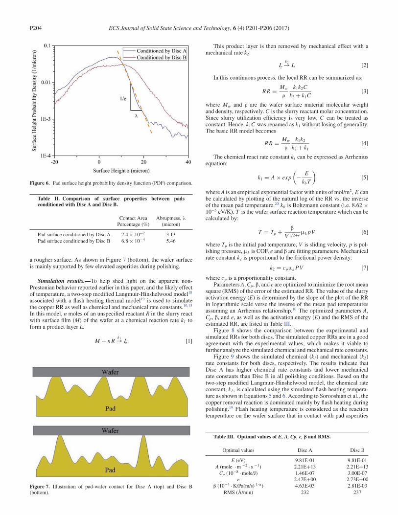
P204 ECS Journal of Solid State Science and Technology, 6 (4) P201-P206 (2017)
Figure 6. Pad surface height probability density function (PDF) comparison.
Table II. Comparison of surface properties between padsconditioned with Disc A and Disc B.
Contact Area Abruptness, λPercentage (%) (micron)
Pad surface conditioned by Disc A 2.4× 10⁻² 3.13Pad surface conditioned by Disc B 6.8× 10⁻⁴ 5.46
a rougher surface. As shown in Figure 7 (bottom), the wafer surfaceis mainly supported by few elevated asperities during polishing.
Simulation results.—To help shed light on the apparent non-Prestonian behavior reported earlier in this paper, and the likely effectof temperature, a two-step modified Langmuir-Hinshelwood model18
associated with a flash heating thermal model19 is used to simulatethe copper RR as well as chemical and mechanical rate constants.10,15
In this model, n moles of an unspecified reactant R in the slurry reactwith surface film (M) of the wafer at a chemical reaction rate k1 toform a product layer L.
M + n Rk1→ L− [1]
Figure 7. Illustration of pad-wafer contact for Disc A (top) and Disc B(bottom).
This product layer is then removed by mechanical effect with amechanical rate k2.
L−k2→ L [2]
In this continuous process, the local RR can be summarized as:
R R = Mw
ρ
k1k2C
k2 + k1C[3]
where Mw and ρ are the wafer surface material molecular weightand density, respectively. C is the slurry reactant molar concentration.Since slurry utilization efficiency is very low, C can be treated asconstant. Hence, k1C was renamed as k1 without losing of generality.The basic RR model becomes
R R = Mw
ρ
k1k2k2 + k1
[4]
The chemical react rate constant k1 can be expressed as Arrheniusequation:
k1 = A × exp
(− E
kbT
)[5]
whereA is an empirical exponential factor with units of mol/m2, E canbe calculated by plotting of the natural log of the RR vs. the inverseof the mean pad temperature.20 kb is Boltzmann constant (i.e. 8.62 ×10⁻⁵ eV/K). T is the wafer surface reaction temperature which can becalculated by:
T = Tp + β
V 1/2+eμk pV [6]
where Tp is the initial pad temperature, V is sliding velocity, p is pol-ishing pressure, μk is COF, e and β are fitting parameters. Mechanicalrate constant k2 is proportional to the frictional power density:
k2 = cpμk PV [7]
where cp is a proportionality constant.Parameters A,Cp, β, and e are optimized to minimize the root mean
square (RMS) of the error of the estimated RR. The value of the slurryactivation energy (E) is determined by the slope of the plot of the RRin logarithmic scale verse the inverse of the mean pad temperaturesassuming an Arrhenius relationship.10 The optimized parameters A,Cp, β, and e, as well as the activation energy (E) and the RMS of theestimated RR, are listed in Table III.Figure 8 shows the comparison between the experimental and
simulated RRs for both discs. The simulated copper RRs are in a goodagreement with the experimental values, which makes it viable tofurther analyze the simulated chemical and mechanical rate constants.Figure 9 shows the simulated chemical (k1) and mechanical (k2)
rate constants for both discs, respectively. The results indicate thatDisc A has higher chemical rate constants and lower mechanicalrate constants than Disc B in all polishing conditions. Based on thetwo-step modified Langmuir-Hinshelwood model, the chemical rateconstant, k1, is calculated using the simulated flash heating tempera-ture as shown in Equations 5 and 6. According to Sorooshian et al., thecopper removal reaction is dominated mainly by flash heating duringpolishing.19 Flash heating temperature is considered as the reactiontemperature on the wafer surface that in contact with pad asperities
Table III. Optimal values of E, A, Cp, e, β and RMS.
Optimal values Disc A Disc B
E (eV) 9.81E-01 9.81E-01A (mole ·m −2 · s −1) 2.21E+13 2.21E+13
Cp (10−8 ·mole/J) 1.46E-07 3.00E-07e 2.47E+00 2.73E+00
β (10−4 ·K/Pa(m/s) 1-α) 4.63E-03 2.81E-03RMS (Å/min) 232 237
) unless CC License in place (see abstract). ecsdl.org/site/terms_use address. Redistribution subject to ECS terms of use (see 150.135.210.197Downloaded on 2017-03-08 to IP

ECS Journal of Solid State Science and Technology, 6 (4) P201-P206 (2017) P205
Figure 8. Comparison of experimental and simulated copper RR for Disc A(top) and Disc B (bottom).
during polishing.19 As a result, the flash heating temperature is ex-pected to be affected by the pad asperities that generated differentlyby the two discs. Figure 10 shows that Disc A has significantly highersimulated flash heating temperature than Disc B. Consequently, DiscA results in higher simulated chemical rate constant, k1, than DiscB. It must be noted the ratio of simulated k1 to k2 (i.e. k1/k2) is, attimes, more important than the individual value of k1 and k2 itself asthe value of k1/k2 can indicate the controlling removal mechanism. Ingeneral, if the value of k1/k2 is less than 1, the polishing mechanismis, therefore, a chemically limited process. On the other hand, whenthe value of k1/k2 is greater than 1, the polishing process becomesmechanically limited. Furthermore, when the value of k1/k2 is equalto 1, the polishing process is considered chemically and mechanicallybalanced. Figure 11 shows the ratios of the simulated chemical rateto simulated mechanical rate constants (k1/k2). For Disc A, while thesimulated k1/k2 values reduces with the increase of P×V, the polishingprocess stays at mechanically limited process at all of the polishingconditions tested in this study. In addition, the polishing process isstrongly mechanically limited at low P×V conditions. For Disc B, thepolishing process is mechanically limited at low P×V conditions. Athigh P×V conditions, the polishing process becomes chemically andmechanically balanced. In general, Disc A induces a more mechani-cally limited polishing process than Disc B.
Figure 9. Simulated chemical rate constant k1 (top) and mechanical rate con-stant k2 (bottom) for Disc A and Disc B.
Figure 10. Simulated wafer surface reaction temperatures for Disc A andDisc B.
Conclusions
In this study, the effect of different pad surface micro-textures onthe tribological, thermal and kinetic attributes during copper chemi-cal mechanical planarization (CMP) was investigated. The differentmicro-textures were generated by two different chemical vapor de-posited (CVD) diamond-coated conditioner discs (i.e. Disc A andDisc B). Disc A generated significantly higher values of coefficientof friction (COF) and removal rate compared to Disc B. Pad sampleswere taken after wafer polishing and pad surface contact area andtopography were analyzed using laser confocal microscopy. Resultsshowed that Disc A generated a surface with smaller abruptness (λ)and a narrow surface height distribution which indicated that surfaceasperities were more uniform, therefore leading to larger solid con-tact area. In contrast, Disc B generated a pad surface with higherabruptness and less contact areas. A two-step modified Langmuir–Hinshelwood model was employed to simulate copper removal ratesas well as chemical and mechanical rate constants. The simulatedchemical rate to mechanical rate constant ratios indicated that Disc Aproduced a more mechanically limited process than Disc B in all pol-ishing conditions tested in this study. The polishing using Disc B was
Figure 11. Simulated k1/k2 for Disc A and Disc B.
) unless CC License in place (see abstract). ecsdl.org/site/terms_use address. Redistribution subject to ECS terms of use (see 150.135.210.197Downloaded on 2017-03-08 to IP

P206 ECS Journal of Solid State Science and Technology, 6 (4) P201-P206 (2017)
leaning toward mechanically limited process at low P×V conditionsand it became chemically and mechanically balanced at high P×Vconditions.
References
1. M. Krishnan, J. W. Nalaskowski, and L. M. Cook, Chem. Rev., 110, 178 (2010).2. D. Stein, D. Hetherington, M. Dugger, and T. Stout, J. Electron. Mater., 25, 1623(1996).
3. Z. Stavreva, D. Zeidler, M. Plotner, and K. Drescher, Appl. Surf. Sci., 108, 39(1997).
4. C. Lee, H. Lee, M. Jeong, and H. Jeong, Int. J. Precis. Eng. Man., 12, 917(2011).
5. K. Park and H. Jeong, J. Electrochem. Soc., 155, H595 (2008).6. T. Sun, L. Borucki, Y. Zhuang, Y. Sampurno, F. Sudargho, X. Wei, S. Anjur, andA. Philipossian, Jpn. J. Appl. Phys., 49, 026501 (2010).
7. Y. Mu, R. Han, Y. Sampurno, Y. Zhuang, and A. Philipossian, ECS J. Solid State Sci.Technol., 5, 345 (2016).
8. L. Borucki, H. Lee, Y. Zhuang, N. Nikita, R. Kikuma, and A. Philipossian, Jpn. J.Appl. Phys., 48, 115502 (2009).
9. Y. Jiao, Y. Sampurno, Y. Zhuang, X.Wei, A. Meled, and A. Philipossian, Jpn. J. Appl.Phys., 50, 05EC02 (2011).
10. Y. Mu, Y. Jiao, Y. Sampurno, Y. Zhuang, S. Theng, and A. Philipossian, Jpn. J. Appl.Phys., 54, 076502 (2015).
11. Y. C. Kim and S. J. L. Kang, Int. J. Mach. Tool. Manu. 51, 565 (2011).12. http://www.aracainc.com/media/pubs/Polisher_and_Tribometer_300mm.pdf.13. T. Sun, Y. Zhuang, L. Borucki, and A. Philipossian, Jpn. J. Appl. Phys., 49, 046501
(2010).14. A. Philipossian and S. Olsen, Jpn. J. Appl. Phys., 42, 6371 (2003).15. Y. Jiao, X. Liao, C. Wu, S. Theng, Y. Zhuang, Y. Sampurno, M. Goldstein, and
A. Philipossian, J. Electrochem. Soc., 159, H255 (2012).16. X. Liao, Y. Zhuang, L. J. Borucki, S. Theng,X.Wei, T.Ashizawa, andA. Philipossian,
Electrochem. Solid-State Lett., 14, H201 (2011).17. T. Sun, L. Borucki, Y. Zhuang, and A. Philipossian, Microelectron. Eng. 87, 553
(2010).18. L. Borucki, H. Lee, Y. Zhuang, N. Nikita, R. Kikuma, and A. Philipossian, Jpn. J.
Appl. Phys., 48, 115502 (2009).19. J. Sorooshian, L. Borucki, R. Timon, D. Stein, D. Hetherington, and A. Philipossian,
J. Tribol., 127, 639 (2005).20. J. Sorooshian, D. DeNardis, L. Charns, Z. Li, F. Shadman, D. Boning,
D. Hetherington, and A. Philipossian, J. Electrochem. Soc. 151, G85 (2004).
) unless CC License in place (see abstract). ecsdl.org/site/terms_use address. Redistribution subject to ECS terms of use (see 150.135.210.197Downloaded on 2017-03-08 to IP

94
Chapter 7. Effect of Various Slurry Injection System Configurations on
Removal Rates of Silicon Dioxide Using a Ceria-Based CMP Slurry

ECS Journal of Solid State Science and Technology, 6 (7) P449-P454 (2017) P4492162-8769/2017/6(7)/P449/6/$37.00 © The Electrochemical Society
Effect of Various Slurry Injection System Configurations onRemoval Rates of Silicon Dioxide Using a Ceria-Based ChemicalMechanical Planarization SlurryRuochen Han,a,∗,z Yasa Sampurno,a,b Matthew Bahr,a Morgan Skillman,a Leonard Borucki,band Ara Philipossiana,b
aDepartment of Chemical and Environmental Engineering, University of Arizona, Tucson, Arizona 85721, USAbAraca Inc., Tucson, Arizona 85718, USA
In this work, the position of the novel slurry injection system (SIS)was optimized to achieve amore cost-effective and environmentallybenign chemical mechanical planarization process using a widely-adopted ceria-based “reverse slurry”. SIS was configured withdifferent angles in order to investigate slurry dilution characteristics caused by residual pad rinsing with ultrapure water (UPW) thataffected silicon dioxide removal rates. UPW dilution effect on removal rate, coefficient of friction and pad surface temperature wasexplained by maintaining a constant dilution ratio for each of the SIS configuration tests. Results indicated that the negative rotationangle of the SIS increased the actual slurry dilution ratio on top of the polishing pad. This generated more Ce3+ which boosted theremoval rate. Application of negatively rotated SIS allowed significantly lower slurry flow rate and/or shorter polishing time leadingto achieve a more environmental friendly semiconductor manufacturing process. Finally, it was confirmed that variations in SISconfiguration had no impact on silicon dioxide to silicon nitride removal rate selectivity.© 2017 The Electrochemical Society. [DOI: 10.1149/2.0311707jss] All rights reserved.
Manuscript submitted April 17, 2017; revised manuscript received May 25, 2017. Published June 6, 2017.
Chemical mechanical planarization (CMP) has been widely usedto achieve both local and global surface planarization suitable for highvolume manufacturing of integrated circuits. CMP’s popularity is dueto its robust ability to provide local and global planarization whileall the time achieving high material removal rates and superior sur-face quality. During CMP, the wafer is pressed face down against arotating polishing pad. During this contact period, a slurry that con-tains abrasive nanoparticles and myriad chemicals, is delivered to thepad surface near its center. Such conventional center-point applica-tion methods (referred to as “Point Application” or “PA” in this study)lead to low slurry utilization efficiency and poor performance. Previ-ous studies that have used a standard slurry applicator have indicatedthat more than 95% of the fresh slurry tends to spin directly off the padsurface without ever entering the pad-wafer interface due to inefficientbow wave formation and inherent centrifugal forces.1,2 Moreover, itis noteworthy to mention that slurry may cost up to 50% of the totalcost of ownership (COO) in a CMP module.2,3 This is partly due tohigh slurry prices in general as well as the above-mentioned inherentlow slurry utilization efficiency. Furthermore, spent slurry that con-tains reaction by-products and pad debris (due to pad conditioningand wear) is continuously generated during polishing. Since polish-ing by-products and debris cause micro-scratches and other defects,4
large amounts of ultrapure water (UPW) are used to rinse the padbetween wafer polishes causing an appreciable amount of UPW toremain on the pad and inside the grooves. Consequently, during thesubsequent wafer polishing process, the fresh slurry is further dilutedby the residual rinse water. This is an issue since most commerciallyavailable CMP slurries result in lower removal rates when they are fur-ther diluted with water. As a result, higher slurry flowrates have to beemployed to compensate for this dilution effect. This goes against thegeneral wish of integrated circuit manufacturers who strive to improveslurry utilization efficiencywithout sacrificing polishing performance.To reduce slurry usage while maintaining an acceptable process
performance (i.e. removal rate, selectivity, planarity and wafer-leveldefects), a novel slurry injection system (SIS) has been introduced1
and continuously improved upon.5–7 By blocking the spent slurryas well as the residual rinse water from re-entering the pad-waferinterface, SIS is able to shorten the mean residence time and lower thedispersion number6 thereby improving slurry utilization efficiency ascompared to the PA method.In shallow trench isolation (STI) CMP processes, slurries using
cerium dioxide (ceria) abrasive nanoparticles are gaining widespread
∗Electrochemical Society Student Member.zE-mail: [email protected]
acceptance due to their superior ability to increase silicon dioxideover silicon nitride removal rate selectivity and also silicon dioxideremoval rate.8–10 It is important to note that in certain ceria slurryformulations, addition of UPW acts to reduce removal rate (what theindustry calls “direct slurries”) while with certain other formulations(“reverse slurries”) adding water promotes material removal.11,12 Wewill discuss these two types of slurries and the theory behind them indetail later on in this study.Our study aims to optimize the position of the SIS on the polisher
in order to obtain a more cost-effective and environmentally benignCMP process using a widely-adopted ceria-based “reverse slurry”.Here, we configure the SIS at various different angles in order toinvestigate slurry dilution characteristics that affect silicon dioxideremoval rates. These various SIS configurations will be discussed indetail in the Experimental section. UPW dilution effect on removalrate, coefficient of friction (COF) and pad surface temperature, causedby residual rinsing, is also studied by maintaining a constant dilutionratio for each of the SIS configuration tests. That way, any mixing anddilution effects can be attributed to, and explained by, differences inthe position of the SIS only. Removal rate as a function of slurry flowrate and polishing time is also studied to provide a better understandingof water dilution effects over time. Finally, silicon dioxide to siliconnitride removal rate selectivity tests are done to ensure proper finalrecommendations.
Experimental Apparatus and Procedure
In this study, the standard PA method as well as the SIS were usedto introduce slurry onto the pad surface. Figure 1 shows the top viewof a polisher’s platen equipped with the standard PA method (left) aswell as with the SIS (right). The SIS is generally rectangular in shapeand it gets connected to the injector mount using two rods. The mountis then used to secure the entire assembly to the polisher. A singleslurry inlet port is located on the top of the injector body which alignsto a bottom slurry outlet underneath the body at its trailing edge. Freshslurry is introduced through the slurry line that runs from the slurrystorage tank to the inlet and then flows out through the outlet into achannel that is precision machined at the bottom of the injector body.This helps to evenly spread the fresh slurry during polishing. As theSIS rests stably on the pad surface, its leading edge plays an importantrole in directing the spent slurry and the residual rinse water on top ofthe polishing pad during the process. In recent publications, the SISwas configured to block the spent slurry and the residual rinse waterfrom re-entering the pad-wafer interface by directing them toward
) unless CC License in place (see abstract). ecsdl.org/site/terms_use address. Redistribution subject to ECS terms of use (see 150.135.165.47Downloaded on 2017-06-07 to IP

P450 ECS Journal of Solid State Science and Technology, 6 (7) P449-P454 (2017)
Figure 1. Top views of a polisher with point application (left), and the novelslurry injection system (right).
edge of the pad and then on to the drain. General details regarding theSIS can be found elsewhere.13,14
Figure 2 shows the design of the Model X4 SIS injector body(manufactured by Araca) employed in this work. The leading edge ofthe injector body incorporates several “notches”, basically smoothlycurved inner edges of equal size, that are evenly spaced along theleading edge of the injector. During polishing, these “notches” allowthe spent slurry to stay on pad for a slightly longer time thus makingit possible for more of the spent slurry to re-enter the pad-waferinterface.6
All polishing tests were performed on an Araca APD-800X pol-isher. The system is equipped with force transducers suitable foracquiring downforce and shear force in real-time at 1,000 Hz thusallowing the accurate reporting of the instantaneous pad-slurry-waferCOF.15 An interface template with a retaining ring and wetted back-ing film assembly was fitted onto the carrier head using the existingvacuum available through the head. The wafer was securely held by awetted backing film via capillary forces. All input and output param-eters (except for material removal rate) associated with the polishingprocess were automated, controlled and acquired via a proprietarysoftware (written in LabView) developed specifically for our pur-poses.Prior to polishing and data acquisition, an IC1000 k-groove con-
centric pad (manufactured byDow)was broken-in for 60minutes withUPW. The pad break-in was performed using a A165 (by 3M) dia-mond disc conditioner with a rotation speed of 95 RPM and a sweepfrequency of 10 times per minute at a load of 44.5 N. The diamonddisc, pad, and wafer rotation were all counter clockwise. The break-inprocess was followed by polishing several dummy wafers to confirmwhether the pad had reached steady-state condition by monitoring theCOF and determining whether it had stopped changing over time.The above break-in recipe was also used for subsequent in-situ con-
Figure 2. Bottom view of the SIS used in this work (reproduced from Ref. 6).
ditioning (i.e. during the polishing experiments) to ensure sufficientregeneration of the pad micro-texture. Before and after polishing, areflectometer (by SENTECH Instruments GmbH) was used to mea-sure the silicon dioxide film thickness which allowed the calculationof the removal rate for each 300 mm in diameter monitor wafer foreach test.A widely popular ceria-based CMP slurry was used. For all SIS
angle studies, we used the manufacturer’s recommended mixing ratioof 1 part slurry to 2 parts of UPW and maintained the flowrate at 100ml/min. In subsequent flowrate studies, we systematically adoptedset-points of 100, 175 and 250 ml/min. Total polish times in mostcases was 20 s except for when we chose to study how removal ratechanged with total polish time. In those cases, polishing times wereset to 5, 10, 20, 30, 45 or 60 s. Each wafer was polished at a fixedpolishing pressure of 6 PSI and a fixed sliding velocity of 1.8 m/s. Anumber of repeat runs were performed for most conditions to ensureconsistency.In order to alter the slurry flow on the pad surface (i.e. the extent
of fresh slurry that would get mixed with residual used slurry nearthe pad-wafer interface), SIS was installed and configured at variousangles with respect to thewafer. In its most common configuration, thebody of the SIS was rotated slightly in a counterclockwise directionrelative to the platen’s radial passing through the center of the injectorbody’s leading edge. This was done to direct residual slurry (that alsocontained some rinse water) off of the pad and toward the edge, thusreducing the residence time.Figure 3 shows an enlarged schematic of how we have defined the
SIS rotation angle. When the leading edge is overlapping with thediameter, the SIS is in its neutral position (i.e. 0◦). On a counterclock-wise polisher (i.e. in the case of our APD-800X polisher), the angleis defined negative when the injector is rotated clockwise relative tothe diameter. Likewise, the rotation angle becomes positive when theinjector is rotated counterclockwise relative to the diameter.
Results and Discussion
Figure 4 summarizes how silicon dioxide removal rate changeswhen the position of the SIS is changed from one extreme to another(i.e. from −10◦ to +12◦). For purposes of comparison it must benoted that the removal rate associated with the PA slurry dispensemethod is 1,707 Å/min (not shown in Figure 4). During this SISrotation angle test, pad rinsing using UPW is performed in betweenpolishes. Previous study based on real-time videography in the frontof the retaining ring16 shown that the position of the SIS dramaticallyaffects the fluid dynamics of the fresh as well as the spent slurry andresidual rinse water on top of the pad during polishing. The changesare such that when SIS is configured with a positive rotation angle,it tends to block and direct the spent slurry and residual rinse waterto the edge and off the pad. In contrast, when SIS is configured witha negative angle, it tends to retain and direct the spent slurry andresidual rinse water toward the center of the pad and to the retainingring. Figure 4 shows that the configuration of the SIS has a strongimpact on removal rate. The results can be separated into three zonesas delineated in Figure 4. For Zone-I (i.e. from−10◦ to−6◦), removalrates are high and they hover around 2,500 Å/min (far greater thanthe 1,707 Å/min measured for PA). At such negative angles changingthe rotation angle from −10◦ to −6◦, coupled with the “notches”incorporated in the SIS injector bottom design, does not significantlyalter the characteristics of slurry mixing among the freshly injectedslurry, spent slurry and residual rinse water. This has been discussed indetail in a previous study by our research team,16 although in that studya different SIS bottom design was used. In contrast, in Zone-II (i.e.from−6◦ to 0◦), silicon dioxide removal rate drops significantly fromapprox. 2,500 to 1,750 Å/min. Here, as the rotation angle becomesless and less negative, the ability of the SIS to retain spent slurryand residual rinse water decreases dramatically. At 0◦, removal ratebecomes similar to that of the PA method (i.e. 1,740 compared to1,707 Å/min illustrating the SIS has absolutely no advantage over the
) unless CC License in place (see abstract). ecsdl.org/site/terms_use address. Redistribution subject to ECS terms of use (see 150.135.165.47Downloaded on 2017-06-07 to IP

ECS Journal of Solid State Science and Technology, 6 (7) P449-P454 (2017) P451
Figure 3. Schematic of SIS rotation angle: (top) neutral (0◦), (center) positive(+8◦) and (bottom) negative (−8◦).
PA method when it comes to removal rate. In Zone-III (i.e. from 0◦
to 12◦), removal rate decreases further from 1,740 to 1,425 Å/min. Atsuch positive angles, the leading edge of the SIS directs the residualrinsewater and used slurry off of the pad and the freshly injected slurrymixes onlyminimallywith the spent slurry and the residual rinsewater.These series of observations alone are sufficient to conclude that theslurry being used here is indeed a “reverse slurry” where removal ratedrops as the water content of the system is reduced. It should be notedthat in our previous studies with typical silica based “direct slurries”SIS units configured with a positive angle enhanced material removalrates.1,6
To further explore the root cause behind the shape of the removalrate curve for various SIS positions, a series of experiments wereconducted. First, the slurry dilution ratio on the pad was controlledduring polishing without having to actually dilute the slurry withUPW in the pre-mix tank. In typical CMP processes widely used inhigh volume manufacturing, pad rinsing using UPW is performed inbetween polishes. During subsequent polishing, therefore, the residualrinse water on the pad will unavoidably mix with the freshly injectedslurry causing an effectively higher slurry dilution ratio. In the first set
Figure 4. Silicon dioxide removal rate as a function of SIS rotation angle. Forcomparison purposes, the removal rate associated with the PA slurry dispensemethod is 1,707 Å/min.
of experiments, residual pad rinse water was removed from the top ofthe pad (henceforth refer as to the “pad drying process”) prior to thesubsequent wafer polishing. During the “pad drying process”, the padwas continuously rotated at 100 RPM and manually dried by blowingcompressed air on the top of its surface. The air flow swept the padsurface from the center to the edge of the pad thrice prior to eachsubsequent wafer polishing. As such, the pad surface as well as thegrooves reached an equal degree of dryness for each case. This step isnecessary for our controlled slurry dilution study. As a result, residualrinse water was mostly removed from the grooves and the land areasthereby suppressing any chance of slurry dilution due to mixing withresidual rinse water. Following the “pad drying process” and prior towafer polishing, the pad was “primed” using the same 1:2 slurry-to-UPW ratio that was going to be used for polishing. Slurry flow ratekept was constant at 100 ml/min. The SIS having a configuration of−6◦ angle was then employed. As shown in Figure 5, removal ratewas relatively low at 1,125 Å/min, a significant reduction comparedto the 2,500 Å/min obtained at −6◦ with the standard pad rinsingprocedure (Figure 4). Higher dilution ratios were next investigated
Figure 5. Silicon dioxide removal rate as a function of slurry dilution ratio incombination with the SIS at −6◦ and a “pad drying process”.
) unless CC License in place (see abstract). ecsdl.org/site/terms_use address. Redistribution subject to ECS terms of use (see 150.135.165.47Downloaded on 2017-06-07 to IP

P452 ECS Journal of Solid State Science and Technology, 6 (7) P449-P454 (2017)
Figure 6. COF (left) and average pad temperature at the trailing edge of the retaining ring (right) as a function of slurry dilution ratio in combination with the SISat −6◦ and a “pad drying process”.
whereby, each time, the pad was first dried, then primed with slurryand finally used to polish wafers using dilution ratios of 1:5, 1:6, 1:7.5,1:10, 1:15 and 1:20 at point-of-use (POU). This method ensured thatthe same dilution ratio was used during any given polish process withno chance of any residual water participating in the process. As shownin Figure 5, removal rate first increases dramatically as dilution ratiois increases from 1:2 to 1:10 where it reaches a value of 3,100 Å/min.Increasing the dilution further to 1:15 causes the rate to level off (orincrease so slightly to 3,240 Å/min). Finally, diluting the slurry furtherto 1:20 cause a 10 percent drop in removal rate to about 2,800 Å/min.When taken together, Figures 4 and 5 clearly indicate that it is indeedwater dilution to a certain level that causes the removal rate to increasegiven our particular “reverse slurry”.11,12 Most importantly, results ofFigure 5 indicate that polishing with the SIS configured at−6◦ with astarting ratio of 1:2 and a standard rinsing process (as shown in Figure4) behaved as though the wafer was being polished with an effectivedilution ratio of 1:6.According to Wang et al., as water content is increased, more
reactive Ce3+ species are formed on the surface of the abrasive nano-particle which tend to boost silicon dioxide removal rate.11 BesidesWang’s, several other models have been reported that explain theremoval mechanism of ceria slurry in achieving high silicon dioxideremoval rates.17–19 Cook’s proposed removal mechanism is based onthe fact that the hydration layer around the ceria nano-particle surfacehas Ce-OH sites.17 The active -Si-O- sites on oxide surface reactwith the Ce-OH to form Ce-O-Si bonds, which are stronger than the-Si-O- structures on the oxide surface. The reaction products are thenremoved bymechanical friction caused by the pad as well as the activeceria nano-particles. Furthermore, according to several studies,11,18,19
the Ce3+ species that forms on the abrasive particle is highly reactivewhich bonds with -Si-O- structures. On the other hand, Manivannanet al. indicated that Ce4+ (i.e. from CeO2) does not react stronglywith the -Si-O- structures. Thus, Ce3+ is the species that plays acritical role in the “chemical” action in CMP. Furthermore, in aqueoussolutions, Ce(OH)3 is more thermionically stable than CeO2 as ittends to give off oxygen and reduce to the trivalent state.20 Withdilution, CeO2 gets more readily altered to Ce(OH)3 on the abrasivesurface.11 As a result, more Ce3+ ions are generated that break the-Si-O- structures which subsequently act to increase silicon dioxideremoval rates. Such a mechanism is consistent with the results ofour slurry dilution experiment. That is, when the slurry is at a 1:2dilution ratio, Ce3+ is maintained at a low level and removal rate islow. As the slurry gets diluted from 1:2 to 1:15, the concentration ofCe3+ species increases and results in higher removal rates at the samepolishing conditions (i.e. pressure and sliding velocity). Eventually,
further slurry dilution no longer generates more Ce3+ species whichleads to a net reduction in Ce3+ concentration. This causes removalrate to drop. Based on the above elaboration, the angle rotation ofSIS alters the actual slurry dilution ratio on top of the polishing thatchange the concentration of Ce3+, therefore, affecting silicon dioxideremoval rate.So, the initial rising trend in removal rate can be attributed to
an ever-increasing concentration of Ce3+ species with the additionof water up to a ratio of 1:7.5. Beyond this ratio, it is believed thatmechanical (and some other chemical) effects come into play that par-tially offset the benefits of the chemical binding of the Ce3+ specieswith silicon dioxide. These mechanical effects are due to a reductionin the frictional forces when excessive amounts of water are used.Reduced friction acts to reduce removal rate in two ways: First, at aconstant polishing pressure, it lowers the shear force thereby reducingthe contribution of the “mechanical” component in CMP.21–23 Sec-ond, the reduced COF causes process temperature to drop (since lessfriction translates to less energy dissipation in the form of heat) andreduces the contribution of the “chemical” component in CMP.22,24,25
This is because the chemical rate constant in ceria-based CMP pro-cesses is exponentially dependent on temperature (i.e. via the Arrhe-nius relationship) and has been shown by our research team to have anappreciable apparent activation energy of about 0.43 eV.26 Figures 6and show the trends in COF (left) and average pad surface temperature(right), respectively, for the dilution conditions reported in Figure 5.It is clear that increasing the extent of water dilution beyond 1:7.5clearly reduces COF and the average pad surface temperature whichsupports our explanation above.Figure 7 shows the change in silicon dioxide removal rate as a
function of flow rate for both the SIS (configured at a −6◦ angle)and the PA dispense methods using a standard pad rinsing proce-dure. The manufacturer suggested dilution ratio of 1:2 were usedin this set of experiments. In the case of PA, removal rate starts at1,545 Å/min at slurry flow rate of 100 ml/min and then drops lin-early to 1,182 and 813 Å/min when flow rate is increased to 175 and250 ml/min, respectively. In the case of SIS, removal rate starts at2,403 Å/min at slurry flow rate 100 ml/min. As flow rate is increasedto 175 and 250 ml/min, removal rates decrease to 2,046 Å/min and1,845 Å/min, respectively. The fact that in both cases, rates decreasewith increasing flow is consistent with the removal mechanism basedon the Ce3+ species concentration discussed earlier since the higherthe flow rate the less the extent of dilution by the residual water andspent slurry. We can therefore conclude that by using the SIS dispensemethod configured at −6◦ angle, one can get removal rates that areconsistently higher than the PA method at all slurry flow rates.
) unless CC License in place (see abstract). ecsdl.org/site/terms_use address. Redistribution subject to ECS terms of use (see 150.135.165.47Downloaded on 2017-06-07 to IP

ECS Journal of Solid State Science and Technology, 6 (7) P449-P454 (2017) P453
Figure 7. Silicon dioxide removal rate as a function of slurry flow rate.
Higher slurry dilution and longer mean residence time of the ceria-based slurry during CMP may induce defects. In this case, furtheroptimization of the post-CMP cleaning process may be necessary tominimize wafer-level defects.27 In the meantime, according to Arminiet al.28 and Song et al.,29 small and relatively narrow-sized dispersedceria abrasives can help reducing the defectswithout sacrificing silicondioxide removal rate and its selectivity over silicon nitride. In general,additional information is needed regarding tribology and chemicalreactivity of the ceria-based slurry to accurately correlate wafer-leveldefects with slurry dilution and mean residence time. Such dedicatedresearch topics are beyond the scope of this study.The COO and the environmental, health, and safety (EHS) ram-
ifications of Figure 7 are huge as the results suggest that, regardlessof flow rate, SIS can boost removal rates by more than 50 percent.This suggests that, in principle, IC makers can reduce slurry usage by50 percent simply because the higher removal rate will allow them tocut their polishing times proportionately. What’s more, in cases wherewafer throughput of a polisher is removal rate limited (i.e. as opposedto being limited to wafer handling, rinsing or post-CMP cleaning) a50 percent drop in polish time can significantly boost wafer through-put and CMP module efficiency while reducing the COO associatedwith consumables and also avoid certain future capital expenditures asmore wafers may be processed without having to buy more polishersin the future. Lastly, since many slurries (including the ceria-based
Table I. Removal rate comparison between silicon oxide andsilicon nitride.
Silicon dioxide Silicon nitrideRR (Å/min) RR (Å/min)
SIS 100 ml/min 1,508 20PA 250 ml/min 826 20
ones) tend to contain hazardous chemicals, reducing their usage willsignificantly reduce EHS issues.Figure 8 (left) shows the total amount of silicon dioxide removal
as a function of polishing time for both the SIS (configured at −6◦)and the PA dispense methods using a standard pad rinsing procedure.In these tests, blanket silicon dioxide wafers were polished for var-ious times, namely 5, 10, 20, 30, 45 or 60 s using a standard 1:2dilution slurry at 100 ml/min. Results show that the amount removedincreases significantly only during the first 20 s of polishing afterwhich it becomes an asymptote for both dispense methods. To bet-ter understand this data, Figure 8 (right) is constructed which showsthe average removal rate for each segment of the polishing time. Forexample, the removal rate data shown at 15 s in Figure 8 (right) iscalculated by, first, subtracting the total amount removed at 20 s fromthat removed at 10 s (based on Figure 8 left) and then dividing theremoval difference by the time difference (i.e. 10 s). Figure 8 (right)clearly shows removal rates for both the SIS and the PA dispensemethods drop exponentially with longer polish times such that af-ter 35 s, removal rates become nearly zero. This is due to the factthat with the standard pad rinsing procedure, there exists an appre-ciable amount residual water on the pad surface which significantlydilutes the freshly dispensed slurry during the early seconds of thepolishing time thus causing high initial removal rates which begin todiminish as the amount of residual rinse water and spent slurry onthe pad reduces gradually due to pad-wafer rotation and centrifugalforces that guide the fluid toward the edge of the pad and finallyto drainage. During the second half of the polishing process (i.e.from 35 to 60 s), the freshly dispensed slurry becomes minimallydiluted as most of the residual rinse water has already spun off ofthe pad thus lowering the chemical reaction rate and hence materialremoval.Most ceria-based slurries are known for their superior selectivity
when it comes to the amount of silicon dioxide removed as com-pared to the amount of silicon nitride removed during STI CMPprocesses.8 To study the impact of dilution effects on silicon nitrideremoval rate and selectivity as compared to silicon dioxide, removalrates on blanket silicon dioxide and silicon nitride layers are com-pared (Table I). In the case of SIS at −6◦, the removal rates for
Figure 8. Amount of silicon dioxide removed as a function of polish time (left) and corresponding average removal rate in in each time segment (right).
) unless CC License in place (see abstract). ecsdl.org/site/terms_use address. Redistribution subject to ECS terms of use (see 150.135.165.47Downloaded on 2017-06-07 to IP
P454 ECS Journal of Solid State Science and Technology, 6 (7) P449-P454 (2017)
SiO2 and Si3N4 are 1,508 and 20 Å/min, respectively at 100 ml/min.For the PA dispense method at 250 ml/min, the rates are 826 and20 Å/min, respectively. For both dispense methods Si3N4 rates arefound to remain constant at a low value of 20 Å/min suggesting thatSIS does not alter the desired high-selectivity value of the process.An anionic acrylic polymer based additive is commonly formulatedin ceria-based slurries to prevent contact between the ceria particlesand the surface of the nitride film.30 Since the polishing pressure andsliding velocity are the same, the mechanical contribution to Si3N4removal remains the same for both methods. In a separate study, Oh etal. reported that removal rate of nitride film is governed bymechanicalfactors once the passivation layer of the polymer absorbed on the ni-tride film surface is formed.9 Data of Table I suggest that using the SISdoes not affect the removal rate mechanism of the silicon nitride film.
Conclusions
In this work, our group optimized the position of the novel slurryinjection system (SIS) on the polisher to achieve a more cost-effectiveand environmentally benign chemical mechanical planarization pro-cess using a widely-adopted ceria-based “reverse slurry”. Various SISpositions, achieved by changing its rotation angles, were tested inorder to investigate slurry dilution characteristics caused by residualultrapure water (UPW) from pad rinsing that affect silicon dioxide re-moval rates. The rotation angles were found to correlate well with sil-icon dioxide removal rates. The−6◦ configuration yielded the highestremoval rates for all configurations at an approximate of 2,500 Å/min.The negative angle rotation of SIS increased the actual slurry dilutionratio on top of the polishing pad and generated more Ce3+, therefore,boosting silicon dioxide removal rate. In a separate experiment using−6◦ configuration, silicon dioxide removal rates were found to in-crease with dilution up to a slurry to UPW ratio of 1:15. Beyond thisratio, the removal rate curve leveled off due to excess water reducingthe COF and pad surface temperature. Application of negatively ro-tated SIS allowed significantly lower slurry flow rate and/or shorterpolishing time without sacrificing polishing performance, leading toa more environmental friendly semiconductor manufacturing pro-cess. In addition, it was confirmed that variations in SIS configu-ration had no impact on silicon dioxide to silicon nitride removal rateselectivity.
References
1. A. Meled, Y. Zhuang, Y. A. Sampurno, S. Theng, Y. Jiao, L. Borucki, andA. Philipossian, Jpn. J. Appl. Phys., 50, 05EC01 (2011).
2. A. Philipossian and E. Mitchell, Jpn. J. Appl. Phys., 42, 7259 (2003).3. K. Holland, A. Hurst, and H. Pinder,Micro, 20, 26 (2002).4. J. M. Steigerwald, Proc. of IEDM, 1 (2008).5. A. Philipossian, L. Borucki, Y. Sampurno, and Y. Zhuang, Solid State Phenomena,
219, 143 (2015).6. Y. Mu, R. Han, Y. Sampurno, Y. Zhuang, L. Borucki, and A. Philipossian, ECS J.
Solid State Sci. Technol., 5, 155 (2016).7. C. Wu, Y. Sampurno, X. Liao, Y. Zhuang, L. Borucki, S. Theng, and A. Philipossian,
ECS J. Solid State Sci. Technol., 4, 272 (2015).8. R. Manivannan and S. Ramanathan,Microelectron. Eng., 85, 1748 (2008).9. M. H. Oh, J. S. Nho, S. B. Cho, J. S. Lee, and R. K. Singh, Powder Technol, 206, 239(2011).
10. I. Y. Yoon, J. Y. Jeong, Y. B. Park, D. W. Lee, H. H. Ryu, andW. G. Lee,Electrochem.Solid-State Lett., 5, G19 (2002).
11. L. Wang, K. Zhang, Z. Song, and S. Feng, Appl. Surf. Sci., 253, 4951 (2007).12. S. V. Babu, Advances in Chemical Mechanical Planarization (CMP), Woodhead
Publishing, Cambridge, UK (2016).13. L. Borucki, A. Philipossian, Y. Sampurno, and S. Theng, U.S. Pat. 8197306
(2012).14. L. Borucki, Y. Sampurno, and A. Philipossian, U.S. Pat. 8845395 (2014).15. http://aracainc.com/wp-content/uploads/2015/10/APD800-brochure.pdf16. M. Bahr, Y. Sampurno, R. Han, and A. Philipossian,Micromachines, 8, 170 (2007).17. L. M. Cook, J. Non-Cryst. Solids, 120, 152 (1990).18. R. Manivannan and S. Ramanathan, Appl. Surf. Sci., 255, 3764 (2009).19. P. V. Dandu, B. C. Peethala, and S. V. Babu, J. Electrochem. Soc., 157, H869
(2010).20. M. Pourbaix, Altas of Electrochemical Equilibria in Aqueous Solutions (first English
ed.), Pergamon Press Ltd., London (1966).21. Y. Sampurno, F. Sudargho, Y. Zhuang, T. Ashizawa, H. Morishima, and
A. Philipossian, Electrochem. Solid-State Lett., 12, H191 (2009).22. H. J. Kim, H. Y. Kim, H. D. Jeong, E. S. Lee, and Y. J. Shin, J. Mater. Process. Tech.,
130, 334 (2002).23. L. Borucki, A. Philipossian, and Y. Zhuang, Trans. Electr. Electron. Mater., 8, 79
(2007).24. N. Kim, Y. Seo, and W. Lee, Microelectron. Eng., 83, 362 (2006).25. Z. Li, L. Borucki, I. Koshiyama, and A. Philipossian, J. Electrochem. Soc., 151, G482
(2004).26. Y. Zhuang, L. Borucki, E. Dien, M. Ennahali, G. Michel, B. Laborie, M. Keswani,
D. Rosales-Yeomans, H. Lee, and Ara Philipossian, Trans. Electr. Electron. Mater.,8, 53 (2007).
27. R. Srinivasan, P. V. Dandu, and S. V. Babu, ECS J. Solid State Sci. Technol., 4, P5029(2015).
28. S. Armini, C. M. Whelan, K. Maex, J. L. Hernandez, and M. Moinpour, J. Elec-trochem. Soc., 155, H653 (2008).
29. S. A. Song and S. B. Park, J. Electrochem. Soc., 158, K170 (2011).30. Y. H. Kim, S. K. Kim, N. S. Kim, J. G. Park, and U. Paik, Ultramicroscopy, 108,
1292 (2008).
) unless CC License in place (see abstract). ecsdl.org/site/terms_use address. Redistribution subject to ECS terms of use (see 150.135.165.47Downloaded on 2017-06-07 to IP

101
Chapter 8. Effect of Conditioning and Slurry Application Method on
Silicon Dioxide Removal Rates Using a Ceria-Based CMP Slurry

ECS Journal of Solid State Science and Technology, 6 (7) P477-P482 (2017) P4772162-8769/2017/6(7)/P477/6/$37.00 © The Electrochemical Society
Effect of Conditioning and Slurry Application Method on SiliconDioxide Removal Rates Using a Ceria-Based Chemical MechanicalPlanarization SlurryRuochen Han,a,∗,z Yasa Sampurno,a,b Matthew Bahr,a Leonard Borucki,band Ara Philipossiana,b
aDepartment of Chemical and Environmental Engineering, University of Arizona, Tucson, Arizona 85721, USAbAraca Inc., Tucson, Arizona 85718, USA
In this study, the silicon dioxide removal rate using a “reverse” ceria-based slurry was investigated under four different combinationsof conditioning modes and slurry application methods. In a “reverse” slurry, addition of water acts to promote material removal.Overall, the process using ex-situ conditioning with the slurry injection system (SIS) resulted the highest removal rate, while theprocess using in-situ conditioning with the conventional point application (PA) generated lowest removal rate. This study is aimedto explain the differences in silicon dioxide removal rate based on the variations of the actual slurry dilution ratio on top of thepad associated with conditioning and slurry application methods. The frictional analysis and Stribeck+ curves were employed toelucidate the tribological characteristics. The results showed that the conditioning modes and the slurry application methods variedthe extent of the polishing vibrations. The silicon dioxide removal rate was found to linearly correlate with the extent of COFfluctuation. This work also underscored the importance of optimum slurry flow dynamics and injection geometry for obtaining amore cost-effective and environmentally benign chemical mechanical planarization process.© 2017 The Electrochemical Society. [DOI: 10.1149/2.0371707jss] All rights reserved.
Manuscript submitted April 28, 2017; revised manuscript received June 2, 2017. Published June 14, 2017.
For the past several decades, chemical mechanical planarization(CMP) has been widely used in integrated circuit (IC) fabrication toachieve both local and global surface planarity. CMP significantly sim-plifies the task of fabricating multilayer IC devices while meeting theever-stringent depth of focus requirements of photolithography. CMPenables unprecedented device yields, while reducing overall cost andincreasingwafer throughput.DuringCMP, a patternedwafer is pressedface down against a rotating pad (typicallymade of polyurethane) withthe slurry being delivered near the center of the pad. As the polishingpad is continuously pressed, its asperities tend to collapse. This neces-sitates a conditioning process via a rotating diamond disc. Typically,conditioning is done in in-situ (i.e. conditioning while polishing) orex-situ (i.e. conditioning before polishing) modes. In each case, therotating conditioning disc is pressed onto the pad with a certain down-force and move with a certain sweeping frequency that allows dwelltime control.One of the more effective ways to further improving the CMP
process is to employ methods that reduce the module’s cost of own-ership (COO). Studies have shown that the slurry may comprise upto 50% of the total COO.1,2 Several studies have pointed out thatthe conventional point application of the slurry onto the center ofthe pad (here referred to as PA) leads to very low slurry utilizationefficiency and poor performance.1–3 Furthermore, spent slurry thatcontains reaction by-products and pad shavings and debris (due topad conditioning and wear) is continuously generated during polish-ing. As such, large amounts of ultrapure water (UPW) are used to rinsethe pad between wafer polishes to mitigate the micro-scratches andother defects caused by these by-products and debris.4 Consequently,during the subsequent wafer polishing process, the fresh slurry is fur-ther diluted by an appreciable amount of UPW that has remained onthe surface of the pad and inside the grooves. Such rinsing leads tohigher COO since most commercially available CMP slurries result inlower removal rates when they are further diluted with water. Higherslurry flowrates have to be used to compensate for this dilution effect.This goes against the general wish of integrated circuit manufacturerswho strive to improve slurry utilization efficiency without sacrificingpolish performance.To help alleviate some of the issues discussed above, a novel
slurry injection system (here referred to as SIS) is introduced whichhas been shown to reduce slurry usage without sacrificing polishingperformance.5 By blocking the spent slurry as well as the residual
∗Electrochemical Society Student Member.zE-mail: [email protected]
rinse ultrapure water (UPW) from re-entering the pad-wafer inter-face, SIS is capable of improving the slurry utilization efficiency ascomparing to the PA method.3,5–8 Mu et al.9 proved that the SIS iscapable of shortening slurry mean residence time while lowering thedispersion number, therefore providing a theoretical explanation ofthe mechanism of the SIS.In shallow trench isolation (STI) CMP processes, slurries using
cerium dioxide (ceria) abrasive nanoparticles are gaining widespreadacceptance due to their superior ability to increase the silicon diox-ide over silicon nitride removal rate selectivity, while separately in-creasing the silicon dioxide removal rate.10–12 In certain ceria slurryformulations, addition of UPW acts to reduce removal rate (what theindustry calls “direct slurries”) while with certain other formulations(“reverse slurries”) adding water promotes material removal.13,14 Inour previous work,15 the position of the SIS was optimized to achievea more cost-effective and environmentally benign CMP process usinga ceria-based “reverse slurry”. However, it is important to note that allthe experiments in the previous work were done using in-situ condi-tioning. Since the constant sweeping of the conditioner may changethe slurry flow pattern and the amount of residual rinsing UPW, theimpacts of conditioning will be amplified when a “reverse” slurry isused. As such, we believe it will be highly beneficial to investigate theimpact of the conditioning mode in an effort to better understand andoptimize the CMP process when such a slurry is used.Our study aims to investigate silicon dioxide removal rate with a
“reverse” ceria slurry when four different combinations of condition-ing and slurry application methods are used. These various combi-nations will be discussed in detail in the Experimental section. Thefrictional analysis and Stribeck+ curves are employed to fundamen-tally elucidate the impact of the conditioning method on the tribolog-ical characteristics. The systematic study of slurry, conditioning andremoval rate is explored with respect to COF fluctuations and stick-slip phenomena. Finally, the removal rate is correlated to the extentof process vibration which helps provide a better understanding of“reverse” ceria slurry removal characteristics.
Experimental Apparatus and Procedure
Figure 1 shows the top view of a polisher’s platen with the stan-dard PA method (left) and the SIS (right). The SIS has a rectangularshape design which connects to the injector mount using two rods.The injector mount is then used to secure the entire assembly to thepolisher. A single slurry inlet port is located on the top of the injector’sbody which aligns to a bottom slurry outlet underneath the body (at
) unless CC License in place (see abstract). ecsdl.org/site/terms_use address. Redistribution subject to ECS terms of use (see 150.135.165.42Downloaded on 2017-06-15 to IP

P478 ECS Journal of Solid State Science and Technology, 6 (7) P477-P482 (2017)
Figure 1. Top views of a polisher with point application (left), and the novelslurry injection system (right).
the trailing edge). Fresh slurry is introduced through the slurry linefrom the slurry storage tank to the inlet and then flows out through theoutlet into a precision-machined channel at the bottom of the injec-tor’s body. The channel helps to evenly spread the fresh slurry duringpolishing. The bottom segment contains several “notches”. These aresmoothly curved inner edges of equal size that are evenly spacedalong the leading edge of the injector.9 The SIS body is rotated to−6◦. The definition of this rotation angle has been described in detailelsewhere.15
This particular configuration is adopted in order to direct residualslurry (that also contains some rinse water) off of the pad and towardthe edge, thus reducing residence time. With the SIS placed on thepad surface, spent slurry and residual UPW during wafer polishingare somewhat retained and prevented from re-entering the pad-waferinterface time and time again. Details on the SIS and its principle ofoperation are reported elsewhere.16,17
All polishing tests were performed on an Araca APD-800X pol-isher and tribometer. The system is equipped with force transducerssuitable for acquiring real-time downforce and shear force at 1,000Hz thus allowing the accurate report of the instantaneous pad-slurry-wafer coefficient of friction (COF).18 APD-800X also indicates thelocation of the conditioner as a function of polishing time. An interfacetemplate with a retaining ring and wetted backing film assembly isfitted onto the carrier head using the existing vacuum of the head. Thewafer is securely hold by a wetted backing film via capillary force.All input and output parameters (except removal rate) associated withthe polishing process are automated, controlled and acquired via aLabView software developed specifically for our purposes.Four combinations of conditioning and slurry application methods
were examined in this work as follows: (a) in-situ conditioning withPA, (b) ex-situ conditioning with PA, (c) in-situ conditioning withSIS, and, (d) ex-situ conditioning with SIS. Prior to polishing and dataacquisition, a IC1000 k-groove concentric pad (manufactured byDow)was broken in for 30 minutes with UPW. It must be noted that severalother groups of researchers have reported similar 30-min break-inconditioning times where a stable pad micro-texture was achievedand the process yielded consistent removal rates.19–21 Pad break-inwas performed with a A165 (by 3M) diamond disc conditioner havinga rotational velocity of 95 RPM and a sweep frequency of 10 times perminute at a load of 44.5N. The diamond disc, pad, andwafer all rotatedcounter-clockwise. The break-in process was followed by polishingseveral dummy wafers to confirm that the pad had reached steady-
state (i.e. when COF measurements no longer changed appreciablywith wafer polishing). The above break-in recipe was also used forin-situ or ex-situ conditioning modes during each polishing to ensuresufficient regeneration of the pad micro-texture. In ex-situ cases, thepad was conditioned for 20s between each run.A widely popular ceria-based CMP slurry was used. For all the
studies, we used the manufacturer’s recommended mixing ratio of1 part slurry to 2 parts of UPW and maintained the flowrate at 100ml/min. Each wafer was polished at a fixed polishing pressure of 6 PSIand a sliding velocity of 1.8 m/s. Several repeat runs were performedto ensure consistency. The polishing pad was rinsed consistentlybetween each run. Before and after each polishing run, the waferswere rinsed, dried and measured using a reflectometer (by SENTECHInstruments GmbH) for determining average removal rates.
Results and Discussion
Table I shows the manner in which conditioning and applicationmethods affect silicon dioxide removal rate. Regardless of the condi-tioningmethod, SIS significantly improves removal rates as comparedto the PA method. The results are consistent with our previous obser-vations where the SIS positioned at a negative rotation angle led tohigher silicon dioxide removal rates compared to the PA method.15
Focusing now on the conditioning methods used, one can clearly seethat ex-situ conditioning consistently improves removal rates com-pared to in-situ conditioning. We do not believe this to be due toany differences in pad micro-texture because, in previous studies, wehad always obtained consistent values for COF and variance of shearforce indicating a stable pad surface micro-texture.22 Besides, it hasbeen shown previously that stable pad micro-texture should have no,or very limited, impact on changes in removal rates.19 However, theremoval rate results in Table I are inconsistent with the typical un-derstanding (i.e. conditioning has no significant impact on removalrate when pad surface micro-texture is stable), indicating that condi-tioning may cause other complications when it comes “reverse” ceriaslurries.In Table I, neither the changes in average COF nor the changes
in pad temperature are sufficient to explain the dramatic differencesin silicon dioxide removal rates. Such results are quite different fromone’s conventional understanding of silicon dioxide CMP where COF(and to some extent, process temperature) is used as an indicator ofremoval rate.23 According to Wang et al.13 and our previous work,15
the dilution ratio of the same “reverse” ceria slurry has a significanteffect on silicon dioxide removal rate. As such, the results in Table Isuggest that the continuous sweeping movement of the disc coupledwith its spinning during the polish process may reduce dilution ascompared to ex-situ conditioning. Numerous observations by our teamhas indicated that at the beginning of polishing, residual rinse water isleft on top of the polishing pad. Then, as slurry is applied near the padcenter, it gets diluted by this residual rinse water. Sampurno et al. hasreported that when a spinning conditioner disc sweeping from the padcenter to the pad edge, it draws fluid and sends it radially outwardsand discharge it from the edge of the pad to drainage.24 This loss ofrinse water and diluted slurry causes an overall lower dilution ratioand decreases removal rates in our “reverse” slurry. Even though thenegatively rotated SIS tends to retain and direct the spent slurry andresidual rinse water toward the center of the pad and to the retainingring, the loss caused by the conditioner’s sweeping and spinning actioncannot be enough mitigated.
Table I. Results for reverse cerium slurry polishing silicon dioxide wafers with four different combinations of conditioning mode and slurryapplication method.
Conditioning Mode with Slurry Application Method In-situ with PA Ex-situ with PA In-situ with SIS Ex-situ with SIS
Removal Rate (Å/min) 1,869 2,445 2,673 2,862Average COF 0.599 0.659 0.616 0.647
Average Pad Temperature (◦C) 48.19 49.75 48.22 48.56
) unless CC License in place (see abstract). ecsdl.org/site/terms_use address. Redistribution subject to ECS terms of use (see 150.135.165.42Downloaded on 2017-06-15 to IP

ECS Journal of Solid State Science and Technology, 6 (7) P477-P482 (2017) P479
Figure 2. COF (top), shear force (bottom, red curve) and downforce (bottom, green curve) as a function of time in combination with in-situ conditioning and PA.
As average COF is an insufficient measure for capturing the tri-bological characteristics arising from the polishing process, frictionalanalyses are employed to further understand the tribological charac-teristics associated with the conditioning method. Figure 2 shows theinstantaneous COF (top) and frictional force (bottom) vs. time forin-situ conditioning coupled with PA. In Figure 2 (top), gross COFfluctuations are observed at the beginning of polishing followed by arapid signal stabilization. As COF is the ratio of shear force to appliednormal downforce, the fluctuations in Figure 2 (top) are essentially de-termined by the fluctuations in the measured forces (Figure 2 bottom)that correspond to intrinsic vibrations of the process as well as thesystem’s stick-slip phenomena taking place among the 3 bodies (i.e.pad, wafer and slurry abrasive particles).25 The vibration represents acoupling between the lateral and vertical displacement or tilt of thecarrier head and the wafer surface.26
Figure 3 shows the instantaneous COF (top) and frictional force(bottom) this time using ex-situ conditioning with PA. Every otherparameter is kept exactly the same as those in Figure 2. In contrast,several discrete but periodically distributed COF clusters are observedwhere the total vibration time is much longer than the in-situ case.Between each cluster, there is a short “stable” period. After about8 seconds, the amplitude becomes gradually smaller and after about12 seconds all signals reach steady-state. Comparing to the in-situcase (Figure 2), these results suggest that the vibration occurs whenthere is sufficient amount of slurry and residual water mixing withlittle fluid loss to the outer edges of the pad. As there is little fluidloss caused by conditioner, vibrations tend to last much longer whenex-situ conditioning is used.Stribeck+ curves27 for the in-situ and the ex-situ condition-
ing cases are shown in Figure 4 which help one gain a deeper
Figure 3. COF (top), shear force (bottom, red curve) and downforce (bottom, green curve) as a function of time in combination with ex-situ conditioning and PA.
) unless CC License in place (see abstract). ecsdl.org/site/terms_use address. Redistribution subject to ECS terms of use (see 150.135.165.42Downloaded on 2017-06-15 to IP

P480 ECS Journal of Solid State Science and Technology, 6 (7) P477-P482 (2017)
Figure 4. Stribeck+ curves corresponding to silicon dioxide CMP using PA with: (left) in-situ conditioning of Figure 2, (right) ex-situ conditioning of Figure 3.
understanding of the fluctuations and clusters seen in Figures 2 and3. Different from traditional Stribeck curves (i.e. plots of COF versusthe Sommerfeld number), Stribeck+ curves allow the instantaneousmeasurement of downforce and shear force throughout the polish-ing process resulting in an instantaneous calculation and recording ofthe COF. Thus, Stribeck+ curves are capable of giving a better pic-ture of what may be going on, tribologically, in the pad-slurry-waferinterface.27
Both cases show similarly large slanted COF clusters of 20,000data points, but with different extents and amplitudes. Such shapesindicate the presence of strong up-and-down vibrations in the platenand/or the polishing head.27 Since we know the sliding velocity to bequite constant at all times, these slants must be due to gross changes(i.e. up to 2X) in downforce. As for sideways vibrations, by definition,both shear force and downforce are contributing factors. In the caseof ex-situ conditioning (Figure 4, right) COF shows a similar spread(i.e. amplitude) but the cluster density clearly shows that vibrationslinger for long periods of time. Plotting the data this way offers an
excellent way of visualizing myriad vibration modes in CMP havingdifferent process parameters.Furthermore, CMP processes using a “reverse” ceria slurry show
a completely different tribological behavior as compared to processeswith standard silica-based slurries where only vertical COF clusterswere observed by our team.28 This indicates that, for silica-basedslurries, the actual v/P (i.e. downforce) varies only slightly while forceria slurries, downforce fluctuations are roughly equivalent (or evengreater than) shear force fluctuations. As such, one may need to beconscious of the negative impact ceria-based slurries may have on padwear and wafer-level defects.Figures 5 and 6 show the instantaneous COF (top) and frictional
force (bottom) as a function of time using the SIS with in-situ andex-situ conditioningmodes, respectively. All other parameters are keptexactly the same as those in Figures 2 and 3. Although periodic vibra-tions with similar COF amplitudes are again present, it is clear thatthe force signatures associated with both SIS processes are differentfrom their PA counterparts in several ways.
Figure 5. COF (top), shear force (bottom, red curve) and downforce (bottom, green curve) as a function of time in combination with in-situ conditioning and theSIS.
) unless CC License in place (see abstract). ecsdl.org/site/terms_use address. Redistribution subject to ECS terms of use (see 150.135.165.42Downloaded on 2017-06-15 to IP

ECS Journal of Solid State Science and Technology, 6 (7) P477-P482 (2017) P481
Figure 6. COF (top), shear force (bottom, red curve) and downforce (bottom, green curve) as a function of time in combination with ex-situ conditioning and theSIS.
First, in in-situ mode, COF fluctuations linger for a longer time(i.e. 8 or so seconds instead of 3). Second, in ex-situ mode, COFfluctuations linger for a shorter time (i.e. 9 or so seconds instead of11), but no intermediate regions of stability can be seen in betweenthe periodic COF bursts. Results shown in Figures 5 and 6 clearlyindicate that the negatively rotated SIS is effective in retaining anddirecting the spent slurry and residual rinse water toward the centerof the pad, resulting in sufficient mixing of slurry with residual water,and with little fluid loss to the outer edges of the pad. As a result,vibration occurs quite consistently during the first 8–9 s of polishingin both SIS cases. Such an observation is in good agreement withthe PA method in combination with ex-situ conditioning as explainedusing Figure 3 where vibrations occur when there is sufficient mixingbetween slurry and residual rinse water. Similarly, compared to in-situ conditioning, ex-situ conditioning in conjunction with the SISalso creates stronger and slightly longer vibrations as there is no fluidloss caused by not having a conditioner. Even though the negatively
rotated SIS is capable of retaining the spent slurry and residual rinsewater, the loss caused by the conditioner’s sweeping and spinningaction is unavoidable. Stribeck+ curves for the in-situ and the ex-situconditioning cases using SIS are shown in Figure 7. As expected,the cluster density on both SIS cases clearly shows that vibrationslinger for long periods of time. Such cluster densities are similar tothe Stribeck+ curve of the PA method with ex-situ conditioning asshown in Figure 4 (right).Figure 8 shows the correlation between silicon dioxide removal
rate and relative standard deviation (RSD) of COF for each combina-tion of conditioning mode and slurry application methods. Values foreach case are computed from 20,000 available data points from thecorresponding Stribeck+ curves.Such a correlation is consistent with Carter et al.’s work where
a correlation between shaft vibration intensity and blanket silicondioxide removal rate using a ceria-based slurry was reported.26 In ourcase however, we think the main reason for the observed near-perfect
Figure 7. Stribeck+ curves corresponding to silicon dioxide CMP using SIS: (left) for in-situ conditioning reported in Figure 5, (right) for ex-situ conditioningin Figure 6.
) unless CC License in place (see abstract). ecsdl.org/site/terms_use address. Redistribution subject to ECS terms of use (see 150.135.165.42Downloaded on 2017-06-15 to IP

P482 ECS Journal of Solid State Science and Technology, 6 (7) P477-P482 (2017)
Figure 8. Correlation between silicon dioxide removal rate and relative stan-dard deviation of COF for each combination of conditioning mode and slurryapplication method (IS and ES refer to in-situ and ex-situ conditioning,respectively).
correlation is due to the differences in the way the 4 combinations ofslurry application and conditioning methods affect slurry and residualrinse water mixing and the eventual fluid loss through the edges ofthe pad. We cannot directly observe and quantify these effects, butwe know that they manifest themselves in differences in the RSDof COF and the extent of stick-slip present in the process, the latterhaving been shown to directly affect material removal rates.25 Stickinghappens when abrasive particles get embedded in the softened layerpresent on the surface of the substrate surface, which cause materialto wear off thus causing the subsequent slipping effect and a greaterdegree of vibration.25,26
Conclusions
In this work, the silicon dioxide removal rate using a “reverse”ceria-based slurry was investigated under four different combinationsof conditioning modes (i.e. in-situ vs. ex-situ) and slurry applica-tion methods (i.e. conventional point application vs. slurry injectionsystem). Regardless of the conditioning method, the slurry injectionsystem (SIS) significantly improved removal rates as compared tothe conventional point application (PA) method. Furthermore, ex-situconditioning method consistently increased removal rates comparedto in-situ conditioning method. Overall, the process using ex-situ con-ditioning with SIS resulted the highest removal rate, while the processusing in-situ conditioning with PA generated lowest removal rate. Ina reverse slurry, addition of water acts to promotes material removal.
In this study, the differences in silicon dioxide removal rate can bewell explained based on the variations of the actual slurry dilutionratio on top of the pad associated with conditioning and slurry appli-cation methods. The negatively rotated SIS was capable of retainingresidual rinse water and therefore, SIS promoted higher actual slurrydilution. On the other hand, the conditioner’s sweeping and spinningaction during in-situ conditioning delivered residual rinse water ra-dially outwards, discharged it from the outer edge of the pad andtherefore, it reduced the actual slurry dilution. The frictional analy-sis and Stribeck+ curves were employed to elucidate the tribologicalcharacteristics. The results showed that the conditioning modes andthe slurry application methods varied the extent of the polishing vibra-tions. The silicon dioxide removal rate was found to linearly correlatewith the extent of COF fluctuation.
References
1. A. Philipossian and E. Mitchell, Jpn. J. Appl. Phys., 42, 7259 (2003).2. K. Holland, A. Hurst, and H. Pinder,Micro, 20, 26 (2002).3. A. Meled, Y. Zhuang, Y. A. Sampurno, S. Theng, Y. Jiao, L. Borucki, andA. Philipossian, Jpn. J. Appl. Phys., 50, 05EC01 (2011).
4. J. M. Steigerwald, Proc. of IEDM, 1 (2008).5. A. Philipossian, L. Borucki, Y. Sampurno, and Y. Zhuang, Solid State Phenomena,
219, 143 (2015).6. Y. Zhuang, Y. Sampurno, C. Wu, B. Wu, Y. Mu, L. Borucki, A. Philipossian, andR. Yang, ECS Trans, 60, P625 (2014).
7. C. Wu, Y. Sampurno, X. Liao, Y. Zhuang, L. Borucki, S. Theng, and A. Philipossian,ECS J. Solid State Sci. Technol., 4, P272 (2015).
8. C. Wu, PhD Dissertation, University of Arizona, Tucson, AZ (2015).9. Y. Mu, R. Han, Y. Sampurno, Y. Zhuang, L. Borucki, and A. Philipossian, ECS J.
Solid State Sci. Technol., 5, 155 (2016).10. R. Manivannan and S. Ramanathan,Microelectron. Eng., 85, 1748 (2008).11. M. H. Oh, J. S. Nho, S. B. Cho, J. S. Lee, and R. K. Singh, Powder Technol, 206, 239
(2011).12. I. Y. Yoon, J. Y. Jeong, Y. B. Park, D. W. Lee, H. H. Ryu, andW. G. Lee,Electrochem.
Solid-State Lett., 5, G19 (2002).13. L. Wang, K. Zhang, Z. Song, and S. Feng, Appl. Surf. Sci., 253, 4951 (2007).14. S. V. Babu, Advances in Chemical Mechanical Planarization (CMP), Woodhead
Publishing, Cambridge, UK (2016).15. R. Han, Y. Sampurno, M. Bahr, M. Skillman, L. Borucki, and A. Philipossian, ECS
J. Solid State Sci. Technol., 6, 449 (2017).16. L. Borucki, A. Philipossian, Y. Sampurno, and S. Theng, U. S. Pat, 8197306 (2012).17. L. Borucki, Y. Sampurno, and A. Philipossian, U. S. Pat, 8845395 (2014).18. http://aracainc.com/wp-content/uploads/2015/10/APD800-brochure.pdf19. K. H. Park, H. J. Kim, O. M. Chang, and H. D. Jeong, J. Mater. Process. Technol.,
187, 73 (2007).20. H. D. Jeong, K. H. Park, and K. K. Cho, CIRP Ann. Manuf. Technol., 56, 357 (2007).21. B. Vasilev, S. Bott, R. Rzehak, and J. W. Bartha,Microelectron. Eng., 111, 21 (2013).22. R. Han, Y. Sampurno, and A. Philipossian, Tribol. Lett., 62, 18 (2016).23. A. Philipossian and S. Olsen, Jpn. J. Appl. Phys., 42, 6371 (2003).24. Y. Sampurno, L. Borucki, Y. Zhuang, D. Boning, and A. Philipossian, J. Elec-
trochem.Soc., 152, G537 (2005).25. Y. Sampurno, F. Sudargho, Y. Zhuang, M. Goldstein, and A. Philipossian, Thin Solid
Films, 516, 7667 (2008).26. P. W. Carter and T. Werts, J. Electrochem.Soc., 154, H60 (2007).27. R. Han, Y. Sampurno, S. Theng, F. Sudargho, Y. Zhuang, and A. Philipossian, ECS
J. Solid State Sci. Technol., 6, 32 (2017).28. R. Han, Y. Sampurno, S. Theng, F. Sudargho, Y. Zhuang, and A. Philipossian, ECS
J. Solid State Sci. Technol., 6, 161 (2017).
) unless CC License in place (see abstract). ecsdl.org/site/terms_use address. Redistribution subject to ECS terms of use (see 150.135.165.42Downloaded on 2017-06-15 to IP

108
Chapter 9. References

109
1. M. Krishnan, J. W. Nalaskowski and L. M. Cook, Chemical Reviews, 110, 178
(2010).
2. Y. Li, Microelectronic applications of chemical mechanical planarization, John
Wiley & Sons (2007).
3. P. B. Zantye, A. Kumar and A. K. Sikder, Materials Science and Engineering: R:
Reports, 45, 89 (2004).
4. D. Castillo-Mejia, J. Kelchner and S. Beaudoin, Journal of The Electrochemical
Society, 151, G271 (2004).
5. Y.-C. Kao, C.-C. Yu and S.-H. Shen, Microelectronic Engineering, 65, 61 (2003).
6. S.-D. Kim, I.-S. Hwang and K.-S. Choi, Journal of The Electrochemical Society,
150, G450 (2003).
7. L. Si, D. Guo, J. Luo, X. Lu and G. Xie, Journal of Applied Physics, 109, 084335
(2011).
8. S. V. Babu, Advances in Chemical Mechanical Planarization (CMP), Woodhead
Publishing (2016).
9. G. Banerjee and R. L. Rhoades, ECS Transactions, 13, 1 (2008).
10. B. Davarik, C. W. Koburger, R. Schulz, J. D. Warnock, T. Furukawa, M. Jost, Y.
Taur, W. G. Schwittek, J. K. DeBrosse, M. L. Kerbaugh and J. L. Mauer, in
International Technical Digest on Electron Devices Meeting, p. 61 (1989).
11. K. Jeong Deog, S. Dae Won, H. Dong Won, K. Jin Woong, P. Nae Hak and H.
Sang Beom, in VLSI and CAD, 1999. ICVC '99. 6th International Conference on,
p. 214 (1999).
12. D. Edelstein, J. Heidenreich, R. Goldblatt, W. Cote, C. Uzoh, N. Lustig, P. Roper,
T. McDevitt, W. Motsiff, A. Simon, J. Dukovic, R. Wachnik, H. Rathore, R. Schulz,
L. Su, S. Luce and J. Slattery, in International Electron Devices Meeting. IEDM
Technical Digest, p. 773 (1997).
13. R. D. Goldblatt, B. Agarwala, M. B. Anand, E. P. Barth, G. A. Biery, Z. G. Chen,
S. Cohen, J. B. Connolly, A. Cowley, T. Dalton, S. K. Das, C. R. Davis, A. Deutsch,
C. DeWan, D. C. Edelstein, P. A. Emmi, C. G. Faltermeier, J. A. Fitzsimmons, J.
Hedrick, J. E. Heidenreich, C. K. Hu, J. P. Hummel, P. Jones, E. Kaltalioglu, B. E.
Kastenmeier, M. Krishnan, W. F. Landers, E. Liniger, J. Liu, N. E. Lustig, S.
Malhotra, D. K. Manger, V. McGahay, R. Mih, H. A. Nye, S. Purushothaman, H.
A. Rathore, S. C. Seo, T. M. Shaw, A. H. Simon, T. A. Spooner, M. Stetter, R. A.
110
Wachnik and J. G. Ryan, in Proceedings of the IEEE 2000 International
Interconnect Technology Conference, p. 261 (2000).
14. K. Blumenstock, J. Theisen, P. Pan, J. Dulak, A. Ticknor and T. Sandwick, Journal
of Vacuum Science & Technology B: Microelectronics and Nanometer Structures
Processing, Measurement, and Phenomena, 12, 54 (1994).
15. A. Bryant, W. Hansch and T. Mii, in Proceedings of 1994 IEEE International
Electron Devices Meeting, p. 671 (1994).
16. S. Nag, A. Chatterjee, K. Taylor, I. Ali, S. O. Brien, S. Aur, J. D. Luttmer and I. C.
Chen, in International Electron Devices Meeting. Technical Digest, p. 841 (1996).
17. M. Nandakumar, A. Chatterjee, S. Sridhar, K. Joyner, M. Rodder and I. C. Chen,
in International Electron Devices Meeting 1998. Technical Digest (Cat.
No.98CH36217), p. 133 (1998).
18. A. Chatterjee, I. Ali, K. Joyner, D. Mercer, J. Kuehne, M. Mason, A. Esquivel, D.
Rogers, S. O’Brien, P. Mei, S. Murtaza, S. P. Kwok, K. Taylor, S. Nag, G. Hames,
M. Hanratty, H. Marchman, S. Ashburn and I.-C. Chen, Journal of Vacuum Science
& Technology B: Microelectronics and Nanometer Structures Processing,
Measurement, and Phenomena, 15, 1936 (1997).
19. B. Park, Y. Kim, H. Kim, H. Jeong and D. Dornfeld, ECS Transactions, 19, 51
(2009).
20. R. Srinivasan, P. V. Dandu and S. V. Babu, ECS Journal of Solid State Science and
Technology, 4, P5029 (2015).
21. J. T. Pan, D. Ouma, P. Li, D. Boning, F. Redecker, J. Chung and J. Whitby, in VLSI
Multilevel Interconnect Conference, p. 467 (1998).
22. J. Schlueter, Semiconductor international, 22, 123 (1999).
23. Y. H. Hsien, H. K. Hsu, T. C. Tsai, W. Lin, R. P. Huang, C. H. Chen, C. L. Yang
and J. Y. Wu, Microelectronic Engineering, 92, 19 (2012).
24. J. Kavalieros, J. Brask, M. Doczy, C. Barns, M. Metz, S. Datta, R. Chau, M. Prince,
A. Miller and M. Buehler, Facilitating removal of sacrificial layers to form
replacement metal gates, U.S. Patent No. 10/925,458, (2004).
25. C. E. Barns, M. Prince, M. L. Doczy, J. K. Brask and J. Kavalieros, Facilitating
removal of sacrificial layers via implantation to form replacement metal gates, U.S.
Patent No. 7,422,936, (2008).

111
26. M. L. Doczy, J. K. Brask, J. Kavalieros, C. Barns, M. V. Metz, S. Datta and R. S.
Chau, Multilayer metal gate electrode, U.S. Patent No. 7,126,199, (2006).
27. J. M. Steigerwald, in 2008 IEEE International Electron Devices Meeting, p. 1
(2008).
28. K. Mistry, C. Allen, C. Auth, B. Beattie, D. Bergstrom, M. Bost, M. Brazier, M.
Buehler, A. Cappellani, R. Chau, C. H. Choi, G. Ding, K. Fischer, T. Ghani, R.
Grover, W. Han, D. Hanken, M. Hattendorf, J. He, J. Hicks, R. Huessner, D. Ingerly,
P. Jain, R. James, L. Jong, S. Joshi, C. Kenyon, K. Kuhn, K. Lee, H. Liu, J. Maiz,
B. McIntyre, P. Moon, J. Neirynck, S. Pae, C. Parker, D. Parsons, C. Prasad, L.
Pipes, M. Prince, P. Ranade, T. Reynolds, J. Sandford, L. Shifren, J. Sebastian, J.
Seiple, D. Simon, S. Sivakumar, P. Smith, C. Thomas, T. Troeger, P. Vandervoorn,
S. Williams and K. Zawadzki, in 2007 IEEE International Electron Devices
Meeting, p. 247 (2007).
29. K.-H. Bu and B. M. Moudgil, Journal of The Electrochemical Society, 154, H631
(2007).
30. J. M. Steigerwald, S. P. Murarka and R. J. Gutmann, Chemical mechanical
planarization of microelectronic materials, John Wiley & Sons (2008).
31. P. Ma, Q. Luo, A. Sundarrajan, J. Lu, J. Aubuchon, J. Tseng, N. Kumar, M. Okazaki,
Y. Wang, Y. Wang, Y. Chen, M. Naik, I. Emesh and M. Narasimhan, in 2009 IEEE
International Interconnect Technology Conference, p. 38 (2009).
32. P. H. Holloway and G. E. McGuire, Handbook of compound semiconductors:
growth, processing, characterization, and devices, Elsevier (1996).
33. K. Holloway, P. M. Fryer, C. C. Jr., J. M. E. Harper, P. J. Bailey and K. H. Kelleher,
Journal of Applied Physics, 71, 5433 (1992).
34. C. L. Borst, V. Korthuis, G. B. Shinn, J. D. Luttmer, R. J. Gutmann and W. N. Gill,
Thin Solid Films, 385, 281 (2001).
35. http://techcet.com/wp-content/uploads/2014/10/TECHCETCMPUGBerninFrance
R2rev1101014BRoberts.pdf
36. Ching-luan Su, Zhi-Wei Dai, Chi-Wei Lin, Yen-Sheng Liu and L.-W. Liu.,
Polymer-Plastics Technology and Engineering, 52, 90 (2013).
37. T. Suzuki, K. Fujikura, T. Higashiyama and K. Takata, Journal of Histochemistry
& Cytochemistry, 45, 49 (1997).
38. https://bio.umass.edu/microscopy/Guided_Tour_for_LSM_510_and_META.pdf.

112
39. J. B. Pawley and R. B. Masters, Optical Engineering, 35, 2765 (1996).
40. M. Minsky, Scanning, 10, 128 (1988).
41. C. L. Elmufdi and G. P. Muldowney, MRS Proceedings, 914 (2006).
42. R. W. Ditchburn, Light, Blackie and Son, London (1963).
43. T. Sun, L. Borucki, Y. Zhuang and A. Philipossian, Microelectronic Engineering,
87, 553 (2010).
44. X. Liao, Y. Zhuang, L. J. Borucki, S. Theng, X. Wei, T. Ashizawa and A.
Philipossian, Electrochemical and Solid-State Letters, 14, H201 (2011).
45. J. Sorooshian, D. DeNardis, L. Charns, Z. Li, F. Shadman, D. Boning, D.
Hetherington and A. Philipossian, Journal of The Electrochemical Society, 151,
G85 (2004).
46. S. Wolf, Microchip manufacturing, Lattice press Sunset Beach, CA (2004).
47. W. Silvernail and N. Goetzinger, The Glass Industry, 52, 130 (1971).
48. R. K. Iler, The chemistry of silica: solubility, polymerization, colloid and surface
pro perties, and biochemistry, Wiley (1979).
49. T. S. Izumitani, Optical Glass, American Inst. of Physics (1986).
50. M. Tomozawa, K. Yang, H. Li and S. P. Murarka, MRS Proceedings, 337 (1994).
51. L. M. Cook, Journal of Non-Crystalline Solids, 120, 152 (1990).
52. R. Manivannan and S. Ramanathan, Microelectronic Engineering, 85, 1748 (2008).
53. M.-H. Oh, J.-S. Nho, S.-B. Cho, J.-S. Lee and R. K. Singh, Powder Technology,
206, 239 (2011).
54. I. Y. Yoon, J. Y. Jeong, Y. B. Park, D. W. Lee, H. H. Ryu and W. G. Lee
Electrochemical and Solid-State Letters, 5, G19 (2002).
55. A. Kelsall, Glass Technology, 39, 6 (1998).
56. R. Sabia and H. J. Stevens, Machining Science and Technology, 4, 235 (2000).
57. T. Hoshino, Y. Kurata, Y. Terasaki and K. Susa, Journal of Non-Crystalline Solids,
283, 129 (2001).

113
58. P. R. V. Dandu, B. C. Peethala and S. V. Babu, Journal of The Electrochemical
Society, 157, H869 (2010).
59. M. Rühle, Advanced Materials, 9, 195 (1997).
60. Y. Z. Hu, R. J. Gutmann and T. P. Chow, Journal of The Electrochemical Society,
145, 3919 (1998).
61. W. G. America and S. V. Babu, Electrochemical and Solid-State Letters, 7, G327
(2004).
62. T. Du, D. Tamboli, V. Desai and S. Seal, Journal of The Electrochemical Society,
151, G230 (2004).
63. G. Xu, H. Liang, J. Zhao and Y. Li, Journal of The Electrochemical Society, 151,
G688 (2004).
64. V. Nguyen, H. VanKranenburg and P. Woerlee, Microelectronic Engineering, 50,
403 (2000).
65. F. Preston, Journal of the Society of Glass Technology, 11, 214 (1927).
66. A. Philipossian and E. Mitchell, Japanese Journal of Applied Physics, 42, 7259
(2003).
67. F. Zhang and A. Busnaina, Electrochemical and Solid-State Letters, 1, 184 (1998).
68. Q. Luo, S. Ramarajan and S. V. Babu, Thin Solid Films, 335, 160 (1998).
69. A. Philipossian and S. Olsen, Japanese Journal of Applied Physics, 42, 6371 (2003).
70. Y. Jiao, Y. A. Sampurno, Y. Zhuang, X. Wei, A. Meled and A. Philipossian,
Japanese Journal of Applied Physics, 50, 05EC02 (2011).
71. X. Wei, Y. Zhuang, Y. Sampurno, F. Sudargho, C. Wargo, L. Borucki and A.
Philipossian, Electrochemical and Solid-State Letters, 13, H391 (2010).
72. D. DeNardis, Evaluation and modeling of alternative copper and inter-layer
dielectric chemical mechanical planarization technologies, University of Arizona
(2006).
73. C. Rogers, J. Coppeta, L. Racz, A. Philipossian, F. B. Kaufman and D. Bramono,
Journal of Electronic Materials, 27, 1082 (1998).
74. Y. Sampurno, F. Sudargho, Y. Zhuang, M. Goldstein and A. Philipossian, Thin
Solid Films, 516, 7667 (2008).

114
75. R. Han, Y. Sampurno and A. Philipossian, Tribology Letters, 62, 18 (2016).
76. B. Mullany and G. Byrne, Journal of Materials Processing Technology, 132, 28
(2003).
77. H. Liang and G. Helen Xu, Scripta Materialia, 46, 343 (2002).
78. Z. Li, K. Ina, P. Lefevre, I. Koshiyama and A. Philipossian, Journal of The
Electrochemical Society, 152, G299 (2005).
79. H. Liang, Tribology International, 38, 235 (2005).
80. M. D. Hersey, Theory and Research in Lubrication: Foundation for Future
Developments, John Wiley & Sons (1966).
81. X. Lu, M. M. Khonsari and E. R. Gelinck, Journal of Tribology, 128, 789 (2006).
82. K. C. Ludema, Friction, wear, lubrication: a textbook in tribology, CRC press
(1996).
83. E. Estragnat, G. Tang, H. Liang, S. Jahanmir, P. Pei and J. M. Martin, Journal of
Electronic Materials, 33, 334 (2004).