r-string dacee247/fa04/fa04/lectures/l15_f04.pdf · • dac architecture has significant impact on...
TRANSCRIPT
EECS 247 Lecture 15: Data Converters © 2004 H.K. Page 1
EE247Lecture 15
D/A Converters • D/A architecture examples
– Unit element– Binary weighted
• Static performance– Component matching– Architectures
• Unit element• Binary weighted• Segmented
– Dynamic element matching• Dynamic performance
– Glitches• DAC Examples
EECS 247 Lecture 15: Data Converters © 2004 H.K. Page 2
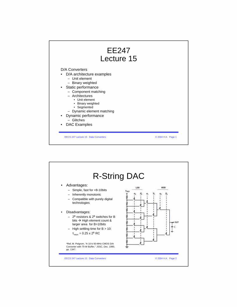
R-String DAC• Advantages:
– Simple, fast for <8-10bits– Inherently monotonic– Compatible with purely digital
technologies
• Disadvantages:– 2B resistors & 2B switches for B
bits à High element count & larger area for B>10bits
– High settling time for B > 10:τmax = 0.25 x 2B RC
*Ref: M. Pelgrom, “A 10-b 50-MHz CMOS D/A Converter with 75-W Buffer,” JSSC, Dec. 1990, pp. 1347.
C

EECS 247 Lecture 15: Data Converters © 2004 H.K. Page 3
R-String DACIncluding Interpolation
Resistor string DACResistor string interpolator increases resolution w/o drastic increase in complexitye.g. 6bit DACà 3+3
Considerations:Interpolation string loading of main R stringLarge R values à less loading but lower speedCan use buffers
Vout
EECS 247 Lecture 15: Data Converters © 2004 H.K. Page 4
R-String DACIncluding Interpolation
Use buffers à Issues: offset & speed

EECS 247 Lecture 15: Data Converters © 2004 H.K. Page 5
Static DAC INL / DNL Errors
• Component matching• Systematic errors
– Contact resistance– Edge effects in capacitor arrays– Process gradient– Finite current source output resistance
• Random errors– Lithography– Often Gaussian distribution (central limit theorem)
*Ref: C. Conroy et al, “Statistical Design Techniques for D/A Converters,” JSSC Aug. 1989, pp. 1118-28.
EECS 247 Lecture 15: Data Converters © 2004 H.K. Page 6
Gaussian Distribution
-3 -2 -1 0 1 2 30
0.05
0.1
0.15
0.2
0.25
0.3
0.35
0.4
x /σ
Pro
babi
lity
dens
ity p
(x)
( )2
2
x
2
2 2
1p( x ) e
2
where standard deviat ion : E( X )
µ
σ
πσ
σ µ
−−
=
= −
EECS 247 Lecture 15: Data Converters © 2004 H.K. Page 7
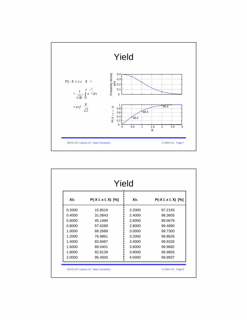
Yield
( )2xX
2
X
P X x X
1e dx
2
Xerf
2
π
+ −
−
− ≤ ≤ + =
=
=
∫ 0
0.1
0.2
0.3
0.4
Pro
babi
lity
dens
ity
p(x)
0 0.5 1 1.5 2 2.5 30
0.20.40.60.8
1
X
38.3
68.3
95.4
P(-
X ≤
x ≤
+X
)
EECS 247 Lecture 15: Data Converters © 2004 H.K. Page 8
Yield
X/σ P(-X ≤ x ≤ X) [%]
0.2000 15.85190.4000 31.08430.6000 45.14940.8000 57.62891.0000 68.26891.2000 76.98611.4000 83.84871.6000 89.04011.8000 92.81392.0000 95.4500
X/σ P(-X ≤ x ≤ X) [%]
2.2000 97.21932.4000 98.36052.6000 99.06782.8000 99.48903.0000 99.73003.2000 99.86263.4000 99.93263.6000 99.96823.8000 99.98554.0000 99.9937

EECS 247 Lecture 15: Data Converters © 2004 H.K. Page 9
Example
• Measurements show that the offset voltage of a batch of operational amplifiers follows a Gaussian distribution with σ = 2mV and µ = 0.
• Fraction of opamps with |Vos| < X = 6mV:– X/σ = 3 à 99.73 % yield (we’d still test before
shipping!)
• Fraction of opamps with |Vos| < X = 400µV:– X/σ = 0.2 à 15.85 % yield
EECS 247 Lecture 15: Data Converters © 2004 H.K. Page 10
Component Mismatch
R
R
∆
10000
100
200
300
400
No.
of r
esis
tors
1004 1008 1012996992988R[ ]Ω
Example: Two side-by-sideResistors
E.g. Let us assume in this example 1000 Rs measured & 68.5% within +-4OHM or +-0.4% of averageà 1σ for resistorsà 0.4%
Large # of devices measured & curved à typically if sample size large shape is Gaussian
EECS 247 Lecture 15: Data Converters © 2004 H.K. Page 11
Component Mismatch
1 2
1 2
2dR
R
R RR
2
dR R R
1
Areaσ
+=
= −
∝
R
R
∆
00
0.05
0.1
0.15
0.2
0.25
0.3
0.35
0.4
Pro
babi
lity
dens
ity p
(x)
σ 2σ 3σ−σ−2σ−3σdR
R
Two side-by-sideResistors
For typical technologies & geometries1σ for resistorsà 0.02 το 5%
In the case of resistors σ is a function of area
EECS 247 Lecture 15: Data Converters © 2004 H.K. Page 12
DNL Unit Element DAC
i i refR I∆ =
DNL of unit element DAC is independent of resolution!
E.g. Resistor string DAC:
Iref
i
i
nom ref
i i ref
nomi
i nom nom nom
nom nom i
DNL dRR
R I
R I
DNL
R R dR dR
R R R
σ σ
∆ =
∆ =
∆ − ∆=
∆
−= = ≈
=

EECS 247 Lecture 15: Data Converters © 2004 H.K. Page 13
DNL Unit Element DAC
Example:If σdR/R = 0.4%, what DNL spec goes into the datasheet so that 99.9% of all converters meet the spec?
Answer:From table: for 99.9% à X/σ = 3.3σDNL = σdR/R = 0.4%3.3 σDNL = 1.3%
àDNL= +/- 0.013 LSBDNL of unit element DAC is independent of resolution!
E.g. Resistor string DAC:
i
i
DNL dR
R
σ σ=
EECS 247 Lecture 15: Data Converters © 2004 H.K. Page 14
DAC INL Analysis
B
A
N=2B-1n
n
N
Output/[Lsb]
Input/[Lsb]
E
Ideal VarianceA n nσε
2
B N-n (N-n)σε2
E = A-n r =n/N= A-r(A+B)= A (1-r) -B.rà Variance of E:
σE2 =(1-r)2 .σΑ
2 + r 2 .σB2
=N.r .(1-r).σε2
àMaximum @ r =0.5, n=N/2àMax INL @ midscale

EECS 247 Lecture 15: Data Converters © 2004 H.K. Page 15
DAC INL
• Error is maximum at mid-scale (N/2):
• INL depends on DAC resolution and element matching σε
• While σDNL = σε
Ref: Kuboki et al, TCAS, 6/1982
2 2E
2E
BINL
B
n1n
Nd
To find max. variance: 0dn
n N / 2
12 1
2 with N 2 1
ε
ε
σ σ
σ
σ σ
−= ×
=
→ =
= −
= −
EECS 247 Lecture 15: Data Converters © 2004 H.K. Page 16
Untrimmed DAC INL
Example:
σINL = 0.1 LSB
σε = 1% B = 8.6σε = 0.5% B = 10.6σε = 0.2% B = 13.3σε = 0.1% B = 15.3
+≅
−≅
ε
ε
σσ
σσ
INL
BINL
B 2log22
1221

EECS 247 Lecture 15: Data Converters © 2004 H.K. Page 17
Simulation Example
σε = 1%B = 12
σINL = 0.3 LSB(midscale)
500 1000 1500 2000 2500 3000 3500 4000-1
0
1
2
bin
DN
L [i
n LS
B]
DNL and INL of 12 Bit converter (from converter decision thresholds)
-0.04 / +0.03 LSB, avg=6.7e-005, std.dev=0.01, range=0.069
500 1000 1500 2000 2500 3000 3500 4000-1
0
1
2
bin
INL
[in
LSB
] -0.2 / +0.8 LSB, avg=0.22, std.dev=0.21, range=0.99
EECS 247 Lecture 15: Data Converters © 2004 H.K. Page 18
Binary Weighted DAC
• INL same as for unit element DAC
• DNL depends on transition– Example:
0 to 1àσDNL2 = σ(dΙ/Ι)
2
1 to 2 àσDNL2 = 3σ(dΙ/Ι)
2
• Consider MSB transition: 0111 … à 1000 …
4 Iref Iref
Iout
2Iref2B-1 Iref
……………

EECS 247 Lecture 15: Data Converters © 2004 H.K. Page 19
MOS Device Matching
d1 d 2d
d d1 d 2
d d
WthLd
WGS thLd
I II
2
dI I I
I I
d dVdIV VI
+=
−=
= + −
Id1 Id2
•Current matching depends on:-Device ratio matching
à larger area less mismatch effect-Threshold voltage matching
à Larger gate-overdrive less threshold voltage mismatch effect
EECS 247 Lecture 15: Data Converters © 2004 H.K. Page 20
Current-Switched DACs in CMOS
WthLd
WGS thLd
d dVdIV VI
= + −
Iout
Iref
……
Switch Array
•Advantages:Can be very fastSmall area for <9-10bits
•Disadvantages:Matching depends on Vth matching & device W/L matching
256 128 64 ………..…..1
Example: 8bit Binary Weighted

EECS 247 Lecture 15: Data Converters © 2004 H.K. Page 21
DNL of Binary Weighted DAC
( ) ( )
DNLmaxB
INL DNLmax max
2 B 1 2 B 1 2DNL
B 2
B / 2
1 12 1
2 2
2 1 2
0111... 1000...
2
2
ε
ε ε
ε
ε
σ σ σ
σ
σ σ
σ σ σ
− −
=
≅ − ≅
= − +
≅
1442443 14243
• Worst-case transition occurs at mid-scale:
• Example:B = 12, σε = 1%àσDNL = 0.64 LSBàσINL = 0.32 LSB
2 4 6 8 10 12 140
5
10
15
DAC input code
σ DN
L2 / σ ε
2
EECS 247 Lecture 15: Data Converters © 2004 H.K. Page 22
Simulation Example
σε = 1%B = 12
σDNL = 0.6 LSB(midscale)
MSB transitions clearly visible
500 1000 1500 2000 2500 3000 3500 4000-1
0
1
2
bin
DN
L [i
n LS
B]
DNL and INL of 12 Bit converter (from converter decision thresholds)
-0.9 / +0.4 LSB, avg=-7.5e-005, std.dev=0.039, range=1.3
500 1000 1500 2000 2500 3000 3500 4000-1
0
1
2
bin
INL
[in
LSB
] -0.7 / +0.7 LSB, avg=3.3e-014, std.dev=0.33, range=1.3

EECS 247 Lecture 15: Data Converters © 2004 H.K. Page 23
“Another” Random Run …
Now (by chance) worst DNL is mid-scale.
Statistical result!500 1000 1500 2000 2500 3000 3500 4000
-2
-1
0
1
2
bin
DN
L [i
n LS
B]
DNL and INL of 12 Bit converter (from converter decision thresholds)
-1 / +0.1 LSB, avg=-9.3e-005, std.dev=0.035, range=1.4
500 1000 1500 2000 2500 3000 3500 4000-1
0
1
2
bin
INL
[in
LSB
] -0.8 / +0.8 LSB, avg=-1.1e-013, std.dev=0.37, range=1.6
EECS 247 Lecture 15: Data Converters © 2004 H.K. Page 24
Unit Element vs Binary Weighted
Unit Element DAC Binary Weighted DAC
B
INL
DNL
S
B
2
2 12
=
≅
=−
ε
ε
σσ
σσ
BS
B
B
INL
INLDNL
=
≅
=≅−
ε
ε
σσ
σσσ12
2
2
22
Number of switched elements:
Significant difference in performance and complexity!

EECS 247 Lecture 15: Data Converters © 2004 H.K. Page 25
Unit Element vs Binary WeightedExample: B=10
Unit Element DAC Binary Weighted DAC
B2
DNL1
INL
B
2 16
S 2 1024
ε
ε ε
σ σσ σ σ−
=≅ =
= =Number of switched elements:
Significant difference in performance and complexity!
B2
B2
DNL1
INL
2 322 16
S B 10
ε ε
ε ε
σ σ σσ σ σ−
≅ =≅ =
= =
EECS 247 Lecture 15: Data Converters © 2004 H.K. Page 26
DAC INL/DNL Summary
• DAC architecture has significant impact on DNL
• INL is independent of DAC architecture and requires element matching commensurate with overall DAC precision
• Results are for uncorrelated random element variations
• Systematic errors and correlations are usually also important
Ref: Kuboki, S.; Kato, K.; Miyakawa, N.; Matsubara, K. Nonlinearity analysis of resistor string A/D converters. IEEE Transactions on Circuits and Systems, vol.CAS-29, (no.6), June 1982. p.383-9.

EECS 247 Lecture 15: Data Converters © 2004 H.K. Page 27
Segmented DAC• Objective:
compromise between unit element and binary weighted DAC
• Approach:B1 MSB bits à unit elementsB2 = B-B1 LSB bits à binary weighted
• INL: unaffected• DNL: worst case occurs when LSB DAC turns off and one more MSB
DAC element turns on: same as binary weighted DAC with B2+1 bits• Number of switched elements: (2B1-1) + B2
Unit Element Binary Weighted
VAnalog
MSB (B1 bits) (B2)LSB
… …
EECS 247 Lecture 15: Data Converters © 2004 H.K. Page 28
ComparisonExample:
B = 12, B1 = 5, B2 = 7B1 = 6, B2 = 6
σε = 1%
( )B 122
B2
DNL INL
1INL
B12
2 2
2
S 2 1 B
ε
ε
σ σ σ
σ σ
+
−
≅ =
≅
= − +
409512
31+763+6
0.010.640.160.113
0.320.320.320.32
Unit element (10+0)Binary weighted(0+10)Segmented 5+7Segmented 6+6
# s.e.σDNL[LSB]σINL[LSB]DAC Architecture
MSB LSB

EECS 247 Lecture 15: Data Converters © 2004 H.K. Page 29
Dynamic DAC Error: Glitch
• Consider binary weighted DAC transition 011 à 100
• DAC output depends on timing
• Plot shows situation where– LSB/MSBs on time– LSB early, MSB late– LSB late, MSB early
1 1.5 2 2.5 30
5
10
idea
l
1 1.5 2 2.5 30
5
10
early
1 1.5 2 2.5 30
5
10
Timela
te
EECS 247 Lecture 15: Data Converters © 2004 H.K. Page 30
Glitch Energy
• Glitch energy (worst case): ~dt x 2B-1
• LSB energy: ~T
• Need dt x 2B-1 << T or dt << 2-B+1 T
• Examples:
<< 488<< 1.5<< 2
121610
120
1000
dt [ps]Bfs [MHz]
EECS 247 Lecture 15: Data Converters © 2004 H.K. Page 31
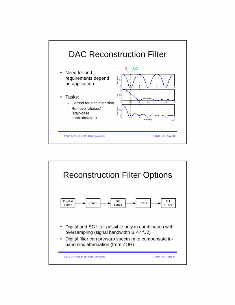
DAC Reconstruction Filter
• Need for and requirements depend on application
• Tasks:– Correct for sinc distortion– Remove “aliases”
(stair-case approximation)
0 0.5 1 1.5 2 2.5 3
x 106
0
0.5
1
DA
C In
put
0 0.5 1 1.5 2 2.5 3
x 106
0
0.5
1
sinc
0 0.5 1 1.5 2 2.5 3
x 106
0
0.5
1
DA
C O
utpu
tFrequency
B fs/2
EECS 247 Lecture 15: Data Converters © 2004 H.K. Page 32
Reconstruction Filter Options
• Digital and SC filter possible only in combination with oversampling (signal bandwidth B << fs/2)
• Digital filter can prewarp spectrum to compensate in-band sinc attenuation (from ZOH)
DigitalF ilter
DAC SCFilter
ZOH CTFilter

EECS 247 Lecture 15: Data Converters © 2004 H.K. Page 33
Sample DAC Implementations
• Untrimmed segmented– T. Miki et al, “An 80-MHz 8-bit CMOS D/A Converter,” JSSC
December 1986, pp. 983.– A. Van den Bosch et al, “A 1-GSample/s Nyquist Current-Steering
CMOS D/A Converter,” JSSC March 2001, pp. 315.• Current copiers:
– D. W. J. Groeneveld et al, “A Self-Calibration Techique for Monolithic High-Resolution D/A Converters,” JSSC December 1989, pp. 1517.
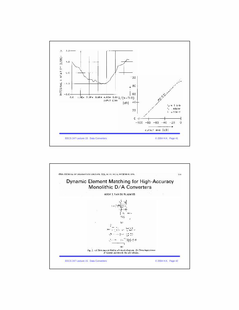
• Dynamic element matching:– R. J. van de Plassche, “Dynamic Element Matching for High-
Accuracy Monolithic D/A Converters,” JSSC December 1976, pp. 795.
EECS 247 Lecture 15: Data Converters © 2004 H.K. Page 34

EECS 247 Lecture 15: Data Converters © 2004 H.K. Page 35
EECS 247 Lecture 15: Data Converters © 2004 H.K. Page 36
Current-Switched DACs in CMOS( )
( )
( )
( )
M 1
M 2 M 1
M 3 M 1
M 4 M 1
M 2
M 1
M 1
M 1
M 1
M 1
M 1
M 1
M 1
2GS th1
GS GS
GS GS
GS GS2
2GS th2 1
GS th
1m
GS th2
m2 1 1 m
2m
3 1 1 m
m4 1
V VI kV V 3RIV V 5RIV V 6RI
3RI1V VI k I
V V2I
gV V
3RgI I I 1 3Rg12
3RgI I I 1 5Rg12
3RgI I 12
−== −= −= −
−−= = − =
−
→ = ≈ −−
→ = ≈ −−
→ = −
( )M 1
2
1 mI 1 6Rg≈ −
Iout
•Assumption: RI is small compared to transistor gate overdriveà Desirable to have gm small
Example: 4 unit element current sources
VDD
I1 I2 I3 I4
3RI 2RI RI
M1 M2 M3 M4

EECS 247 Lecture 15: Data Converters © 2004 H.K. Page 37
Current-Switched DACs in CMOSIout
•Assumption: RI is small compared to xtor gate overdriveà Desirable to have gm small
Example: 4 unit element current sources
VDD
I1 I2 I3 I4
2RI RI
M1 M2 M3 M4
I
I/2 I/2
EECS 247 Lecture 15: Data Converters © 2004 H.K. Page 38

EECS 247 Lecture 15: Data Converters © 2004 H.K. Page 39
EECS 247 Lecture 15: Data Converters © 2004 H.K. Page 40
I
I/2 I/2
Current Divider
EECS 247 Lecture 15: Data Converters © 2004 H.K. Page 41
EECS 247 Lecture 15: Data Converters © 2004 H.K. Page 42

EECS 247 Lecture 15: Data Converters © 2004 H.K. Page 43
EECS 247 Lecture 15: Data Converters © 2004 H.K. Page 44
Dynamic Element Matching
/ 2 error ∆1
I1
( )( )12
1)1(2
121)1(
1
1
1
∆−=
∆+=
o
o
II
II ( )( )12
1)2(2
121)2(
1
1
1
∆+=
∆−=
o
o
II
II
During Φ1 During Φ2
( ) ( )
2
211
2
211
)2(2
)1(2
2
o
o
I
I
III
=
∆++∆−=
+=
I2
fclk
Io
Io/2Io/2
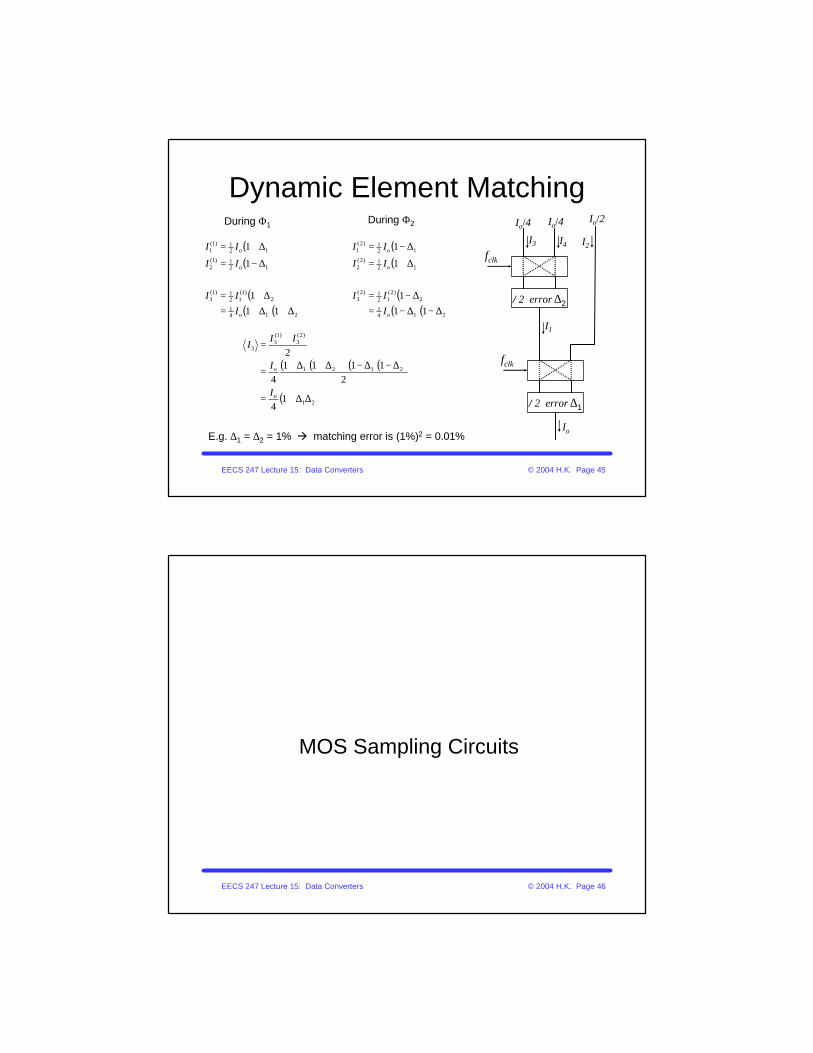
EECS 247 Lecture 15: Data Converters © 2004 H.K. Page 45
Dynamic Element Matching
( )( )
( )( )( )214
1
2)1(
121)1(
3
121)1(
2
121)1(
1
11
1
1
1
∆+∆+=∆+=
∆−=
∆+=
o
o
o
I
II
II
II ( )( )
( )( )( )214
1
2)2(
121)2(
3
121)2(
2
121)2(
1
11
1
1
1
∆−∆−=∆−=
∆+=
∆−=
o
o
o
I
II
II
II
During Φ1 During Φ2
( )( ) ( )( )
( )21
2121
)2(3
)1(3
3
14
21111
4
2
∆∆+=
∆−∆−+∆+∆+=
+=
o
o
I
I
III
E.g. ∆1 = ∆2 = 1% à matching error is (1%)2 = 0.01%
/ 2 error ∆1
I1
I2
fclk
Io
Io/2
/ 2 error ∆2
I3 I4
fclk
Io/4Io/4
EECS 247 Lecture 15: Data Converters © 2004 H.K. Page 46
MOS Sampling Circuits

EECS 247 Lecture 15: Data Converters © 2004 H.K. Page 47
Re-Cap
• How can we build circuits that "sample"
Analog Post processing
D/AConversion
DSP
A/D Conversion
Analog Preprocessing
Analog Input
Analog Output
000...001...
110
Anti-AliasingFilter
Sampling+Quantization
"Bits to Staircase"
Reconstruction Filter
EECS 247 Lecture 15: Data Converters © 2004 H.K. Page 48
Ideal Sampling
• In an ideal world, zero resistance sampling switches would close for the briefest instant to sample a continuous voltage vIN onto the capacitor C
• Not realizable!
vIN vOUT
CS1
φ1
φ1
T=1/fS

EECS 247 Lecture 15: Data Converters © 2004 H.K. Page 49
Ideal T/H Sampling
vIN vOUT
CS1
φ1
• Vout tracks input when switch is closed• Grab exact value of Vin when switch opens• "Track and Hold" (T/H)
φ1
T=1/fS
EECS 247 Lecture 15: Data Converters © 2004 H.K. Page 50
Ideal T/H Sampling
ContinuousTime
T/H signal(SD Signal)
Clock
DT Signal
time

EECS 247 Lecture 15: Data Converters © 2004 H.K. Page 51
Practical Sampling
vIN vOUT
CM1
φ1
• kT/C noise• Finite Rswà limited bandwidth• Rsw = f(Vin) à distortion• Switch charge injection (EE240)• Clock jitter
EECS 247 Lecture 15: Data Converters © 2004 H.K. Page 52
kT/C Noise
In high resolution ADCs kT/C noise usually dominates overall error (power dissipation considerations).
2
2
1212
12
−≥
∆≤
FS
B
B
B
VTkC
CTk
0.003 pF0.8 pF13 pF
206 pF52,800 pF
812141620
Cmin (VFS = 1V)B
EECS 247 Lecture 15: Data Converters © 2004 H.K. Page 53
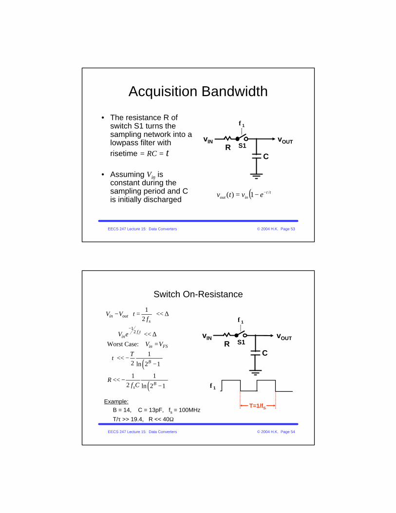
Acquisition Bandwidth
• The resistance R of switch S1 turns the sampling network into a lowpass filter with risetime = RC = τ
• Assuming Vin is constant during the sampling period and C is initially discharged
vIN vOUT
CS1
φ1
R
( )τ/1)( tinout evtv −−=
EECS 247 Lecture 15: Data Converters © 2004 H.K. Page 54
Switch On-Resistance
Example:B = 14, C = 13pF, fs = 100MHz
T/τ >> 19.4, R << 40Ω
vIN vOUT
CS1
φ1
φ1
T=1/fS
R
( )
( )
12
12
Worst Case:
12 ln 2 1
1 12 ln 2 1
s
in outs
fin
in FS
B
Bs
V V tf
V e
V V
T
Rf C
τ
τ
−
− = << ∆
<< ∆=
<< −−
<< −−

EECS 247 Lecture 15: Data Converters © 2004 H.K. Page 55
Switch On-Resistance
( ) ( )
( )
( )( )
0
1,
2
1 1
1 for
1
DS
D triodeDSD triode ox GS TH DS
ON DS V
ON
ox GS th ox DD th in
o
ox DD th
oON
in
DD th
dIW VI C V V V
L R dV
RW W
C V V C V V VL L
RW
C V VL
RR
VV V
µ
µ µ
µ
→
= − − ≅
= =− − −
=−
=−
−
EECS 247 Lecture 15: Data Converters © 2004 H.K. Page 56
Sampling Distortion
in
DD th
outT V
12 V V
in
v
v 1 e τ
− − −
= −
10bit ADC & T/τ = 10VDD – Vth = 2V VFS = 1V

EECS 247 Lecture 15: Data Converters © 2004 H.K. Page 57
Sampling Distortion
10bit ADC T/τ = 20VDD – Vth = 2V VFS = 1V
• SFDR is very sensitive to sampling distortion
• Solutions:• Overdesignà Larger
switchesà increased switch
charge injection• Complementary switch• Maximize VDD/VFSà decreased dynamic range
• Constant VGS ? f(Vin)à …