a 8-bit hybrid architecture current-steering dac · · 2016-04-23volume: 02 issue: 04 ... 1...
TRANSCRIPT

International Research Journal of Engineering and Technology (IRJET) e-ISSN: 2395 -0056
Volume: 02 Issue: 04 | July-2015 www.irjet.net p-ISSN: 2395-0072
© 2015, IRJET ISO 9001:2008 Certified Journal Page 2010
A 8-Bit Hybrid Architecture Current-Steering DAC
Mr. Ganesha H.S.1, Dr. Rekha Bhandarkar2, Ms. Vijayalatha Devadiga3
1 Student, Electronics and communication, N.M.A.M. Institute of Technology, Karnataka, India 2 Professor, Electronics and communication, N.M.A.M. Institute of Technology, , Karnataka, India
3 Assistant Professor, Electronics and communication, Srinivas school of Engineering, Karnataka, India ---------------------------------------------------------------------***---------------------------------------------------------------------
Abstract - Digital to Analog converter (DAC) helps in bridging the digital domain with the everyday analog world. In many telecommunication and Digital Signal Processing circuit’s high resolution and high speed DACs are important building blocks. One of the major applications of DACs is in digital imaging systems like High Definition Television (HDTV). Such applications require high speed, low cost and high resolution data converters. With the above view, an attempt has been made to develop a speed and cost effective of current-steering DAC. There is always a trade-off between precision and cost or area. The proposed hybrid DAC architecture provides a better balance on both precision and cost/area of the implementation. The proposed project presents an 8- bit DAC using hybrid architecture with a switched current matrix, controlled by the six most significant bits, and a conventional 2 bit binary weighted current source controlled by the two least significant bits. The proposed DAC’s sub-blocks is designed using Cadence Virtuoso, 180 nm technology at an operating voltage of 1.8 volts.
Key Words: DAC, Current Matrix, Hybrid Architecture
1. INTRODUCTION
In most of the electronic systems, the input and output signals are analog in nature and uses analog processing devices like amplifiers as input and output devices. Hence, in digital domain, the modification has to be carried out on the input signals and output signals, before and after processing. The need to convert the analog signals into digital signals at the input side, and converting them back into analog signals after processing is significant in real time applications. The circuits that convert analog signals to digital signals are known as Analog to Digital Converters (ADCs) and the circuits that convert digital signal to analog signals are called Digital to Analog Converters (DACs).
The electronics market is emerged to design and produce the products with low power consumption, high speed and portability feature. For high speed data conversion
applications the current-steering DACs are best suitable. Different types of architectures can be used for the implementation of the current-steering DAC. Through a standard design methodology and considering the trade-offs among performance parameters, designers have to optimize each building block to ensure the required performance of the DAC. In trying to arrive at a solution for these problems the proposed hybrid DAC, combines merits of the thermometer current-steering DAC concept for the MSBs and the binary weighted DAC concept for the LSBs. The proposed hybrid DAC architecture is expected to provide a better balance on DAC performance parameter.
1.1 PROBLEM STATEMENT Binary weighted current steering architecture is suitable for high speed and area efficient DAC design. Thermometer coded current steering architecture is suitable for fast and high precision DAC design, but this is at the expense of higher cost in terms of the number of current sources required.
The recent real time applications require high speed, low cost and high resolution data converter. But, there is always a trade-off between precision and cost/area. The proposed hybrid DAC architecture is expected to provide a better balance on both precision and cost/area of the implementation.
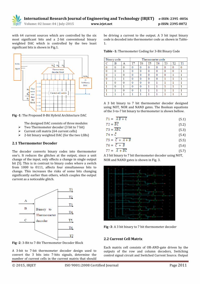
2. The proposed hybrid DAC The proposed hybrid DAC consist of thermometer coded and binary weighted current steered DAC. In this 8-bits input data is divided in two 3-bit chunks [(B7, B6, B5), (B4, B3, B2)] and one 2-bit chunk (B1, B0). The Six MSBs [(B7, B6, B5), (B4, B3, B2)] are connected to the thermometer decoder DAC. The upper chunk (B7, B6, B5) is connected to the thermometer row decoder block and the lower chunk (B4, B3, B2) are connected to the thermometer column decoder block. The two LSBs (one 2-bit chunk i.e., (B1, B0)) are connected to the binary weighted DAC.
Current matrix controlled by the thermometer decoder outputs and a conventional 2-bit current source controlled by the two LSBs. Hybrid DAC which uses a current-matrix
International Research Journal of Engineering and Technology (IRJET) e-ISSN: 2395 -0056
Volume: 02 Issue: 04 | July-2015 www.irjet.net p-ISSN: 2395-0072
© 2015, IRJET ISO 9001:2008 Certified Journal Page 2011
with 64 current sources which are controlled by the six most significant bits and a 2-bit conventional binary weighted DAC which is controlled by the two least significant bits is shown in Fig.1.
Fig -1: The Proposed 8-Bit Hybrid Architecture DAC
The designed DAC consists of three modules Two Thermometer decoder (3 bit to 7 bit) Current cell matrix (64 current cells) 2-bit binary weighted DAC (for the two LSBs)
2.1 Thermometer Decoder
The decoder converts binary codes into thermometer one’s. It reduces the glitches at the output, since a unit change of the input, only effects a change in single output bit [5]. This is in contrast to binary codes where a switch from 1000 to 0111, affects four simultaneous bits to change. This increases the risks of some bits changing significantly earlier than others, which couples the output current as a noticeable glitch.
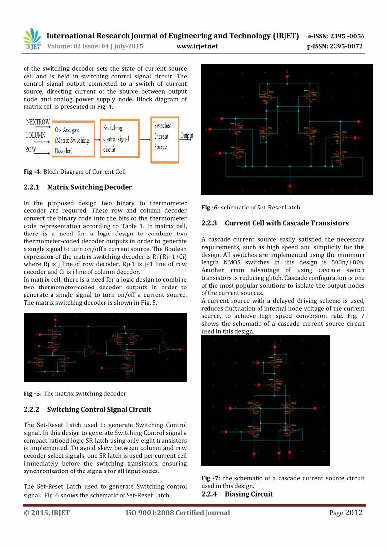
Fig -2: 3-Bit to 7-Bit Thermometer Decoder Block
A 3-bit to 7-bit thermometer decoder design used to convert the 3 bits into 7-bits signals, determine the number of current cells in the current matrix that should
be driving a current to the output. A 3 bit input binary code is decoded into thermometer code as shown in Table-1. Table -1: Thermometer Coding for 3-Bit Binary Code
A 3 bit binary to 7 bit thermometer decoder designed using NOT, NOR and NAND gates. The Boolean equations of the 3-to-7 bit binary to thermometer is shown bellow.
(5.1)
(5.2)
(5.3)
(5.4)
(5.5)
(5.6)
(5.7)
A 3 bit binary to 7 bit thermometer decoder using NOT,
NOR and NAND gates is shown in Fig. 3.
Fig -3: A 3 bit binary to 7 bit thermometer decoder
2.2 Current Cell Matrix Each matrix cell consists of OR-AND-gate driven by the outputs of the row and column decoders, Switching control signal circuit and Switched Current Source. Output
International Research Journal of Engineering and Technology (IRJET) e-ISSN: 2395 -0056
Volume: 02 Issue: 04 | July-2015 www.irjet.net p-ISSN: 2395-0072
© 2015, IRJET ISO 9001:2008 Certified Journal Page 2012
of the switching decoder sets the state of current source cell and is held in switching control signal circuit. The control signal output connected to a switch of current source, directing current of the source between output node and analog power supply node. Block diagram of matrix cell is presented in Fig. 4.
Fig -4: Block Diagram of Current Cell
2.2.1 Matrix Switching Decoder In the proposed design two binary to thermometer decoder are required. These row and column decoder convert the binary code into the bits of the thermometer code representation according to Table 1. In matrix cell, there is a need for a logic design to combine two thermometer-coded decoder outputs in order to generate a single signal to turn on/off a current source. The Boolean expression of the matrix switching decoder is Rj (Rj+1+Ci) where Rj is j line of row decoder, Rj+1 is j+1 line of row decoder and Ci is i line of column decoder. In matrix cell, there is a need for a logic design to combine two thermometer-coded decoder outputs in order to generate a single signal to turn on/off a current source. The matrix switching decoder is shown in Fig. 5.
Fig -5: The matrix switching decoder
2.2.2 Switching Control Signal Circuit The Set-Reset Latch used to generate Switching Control signal. In this design to generate Switching Control signal a compact ratioed logic SR latch using only eight transistors is implemented. To avoid skew between column and row decoder select signals, one SR latch is used per current cell immediately before the switching transistors, ensuring synchronization of the signals for all input codes. The Set-Reset Latch used to generate Switching control
signal. Fig. 6 shows the schematic of Set-Reset Latch.
Fig -6: schematic of Set-Reset Latch
2.2.3 Current Cell with Cascade Transistors A cascade current source easily satisfied the necessary requirements, such as high speed and simplicity for this design. All switches are implemented using the minimum length NMOS switches in this design is 500n/180n. Another main advantage of using cascade switch transistors is reducing glitch. Cascade configuration is one of the most popular solutions to isolate the output nodes of the current sources. A current source with a delayed driving scheme is used, reduces fluctuation of internal node voltage of the current source, to achieve high speed conversion rate. Fig. 7 shows the schematic of a cascade current source circuit used in this design.
Fig -7: the schematic of a cascade current source circuit used in this design.
2.2.4 Biasing Circuit

International Research Journal of Engineering and Technology (IRJET) e-ISSN: 2395 -0056
Volume: 02 Issue: 04 | July-2015 www.irjet.net p-ISSN: 2395-0072
© 2015, IRJET ISO 9001:2008 Certified Journal Page 2013
The biasing circuit is consisting of two transistors, which provide two biasing voltages for all of the current sources. The output current of each current cell is adjusted by changing the biasing voltages. The biasing circuits, as shown in Fig. 8, provide two biasing voltages for all of the current sources.
Fig -8: The biasing circuit
2.3 2-Bit Binary DAC Use of conventional binary weighted designs significantly reduces the layout area of DAC [1] [2], but have less precision. In this design the binary weighted architecture is used for the two LSBs.
3. SIMULATION RESULTS
Fig. 9 shows 8 input signals, Six MSBs signals applied to thermometer decoder DAC and two LSBs applied to binary weighted DAC, one output converted signal for digital value of the Proposed 8-Bit Hybrid Architecture DAC.
Fig -9: The Proposed 8-Bit Hybrid Architecture DAC Fig. 10 shows 8 input signals, Six MSBs signals applied to
thermometer decoder DAC and two LSBs applied to binary
weighted DAC, one output converted signal for digital
value of the Proposed 8-Bit Hybrid Architecture DAC.
Fig -10: Simulation Result of Proposed 8-Bit Hybrid Architecture DAC. Since, it is 8 bit DAC, the step output of the DAC should be 2N steps that means equal to 256 steps. Here in order to find INL and DNL around 15 trials are taken. Non Ideal transfer curve is shown in Fig. 11. The INL and DNL values are calculated and simulation graph for the same is drawn using MS-Excel. Fig. 12 shows the output of Integral non linearity and Fig. 13 shows the output of Differential non linearity along with its theoretical and practical values which has been calculated.
Fig -11: Non Ideal transfer curve
Fig -12: The output of Integral non linearity

International Research Journal of Engineering and Technology (IRJET) e-ISSN: 2395 -0056
Volume: 02 Issue: 04 | July-2015 www.irjet.net p-ISSN: 2395-0072
© 2015, IRJET ISO 9001:2008 Certified Journal Page 2014
Integral Non-Linearity can be calculated using the following formulae: INL= output value for input code n – output value of the reference line at that point For 8-BIT Digital to Analog Converter Integral non- linearity is identified as the + 0.006 to – 0.005. DNL = Actual increment height of transition n - Ideal incremental height For 8-Bit Digital to Analog Converter differential non- linearity is identified as the + 0.006 to – 0.006.
Fig -13: The output of Differential non linearity
4. CONCLUSIONS Different types of architectures can be used for
the implementation of the DAC. Some applications requires balanced speed, cost and resolution data converter. The current steering DAC is suitable for high speed application. The current steering DAC is implemented using thermometer decoder concept to avoid glitch and differential nonlinearity, but more expensive in terms of number of current sources. The binary weighted current steering DAC architecture provides high speed, less area but more glitch and differential nonlinearity.
By considering advantages of both thermometers current steering DAC and binary weighted current steering DAC an 8-bit hybrid current steering DAC is designed. The thermometer coded architecture is used for the six MSBs so it reduces glitches, maintains the monotonic variation and precision. The binary weighed architecture is used for the last two LSBs therefore number of current cells reduced from 256 to 66 cells therefore reduces the area. The Hybrid DAC architecture provides a better balance on DAC performance parameter.
REFERENCES [1] Xu Wu, Pieter Palmers, Michiel S. J. Steyaert, “A 130
nm CMOS 6-bit Full Nyquist3 GS/s DAC”, IEEE Journal on Solid-State Circuits, vol. 43, no. 11, pp.2396-2403, 2007.
[2] Gupta, S. Saxena, V., Campbell, K.A. Baker, R.J., “W-2W Current Steering DAC for Programming Phase Change Memory”,IEEE Workshop on Microelectronics and Electron Devices, vol.14, no. 33, pp.132-136, 2009.
[3] Pieter Palmers, Michiel S. J. Steyaert, “A 10–Bit 1.6-GS/s 27-mW Current-Steering D/A Converter With 550-MHz 54-dB SFDR Bandwidth in 130-nm CMOS”, IEEE Transactions on Circuits and Systems, vol. 57, no. 11, pp.2870-2879, 2010.
[4] I. Myderrizi and A. Zeki “Current-Steering Digital-to-Analog Converters: Functional Specifications, Design Basics, and Behavioural Modelling”, IEEE Antennas and Propagation Magazine, vol. 52, no.4, 2010.
[5] Wei-Sheng Cheng, Min-Han Hsieh, Shuo-Hong Hung, Szu-Yao Hung and Charlie Chung-Ping Chen“A 10-bit Current-Steering DAC for HomePlug AV2 Powerline Communication System in 90nm CMOS”, Circuits and Systems (ISCAS),IEEE International Symposium, pp. 2034-2037,2013.
[6] Astria Nur Irfansyah,Torsten Lehmann, Julian Jenkins, Tara Julia Hamilton, “Design Strategy for Enhanced Output Impedance Current-steering DAC in Sigma-Delta Converters”, Circuits and Systems (MWSCAS), IEEE 56th International Midwest Symposium , pp. 289-292, 2013.
[7] Ms.Anuradha S. Kherde1 Prof.P.R.Gumble“A Review of Various Trends of Digital To-Analog Converter with Performance Characteristics and Behavioural Parameters”, International Journal of Advanced Research in Computer Science and Software Engineering, Vol. 3, Issue 4, pp.508-512, April 2013.
[8] David A. Johns, Ken Martin, “Analog Integrated Circuits Design”, Second Edition, John Wiley & Sons, 1997.