printed circuit transmission sline transitions air force systems command griffiss air force base,...
TRANSCRIPT

RADC-TR-85-24 1In-House ReportDecember 1965 >
C PRINTED CIRCUIT TRANSMISSIONSLINE TRANSITIONS
Frank E. Kozak, CIC, USAFDaniel T. McGrath, Capt, USAF
APPROVED FOR PUBLIC RELESE; DISTRIBUTION UNLIMITED
ROME AIR DEVELOPMENT CENTERAir Force Systems Command
Griffiss Air Force Base, NY 13441-5700

This report has been reviewed by the RADC Public Affairs Office (PA) andis releasable to the National Technical Information Service (NTIS). At NTISit will be releasable to the general public, including foreign nations.
RADC-TR-85-241 has been reviewed and is approved for publication.
* APPROVED:
PAUL H. CARR, Acting ChiefAntennas & RF Components BranchElectromagnetic Sciences Division
mV
APPROVED: /f ,,f ( 1 . ( -
ALLAN C. SCHELLChief, Electromagnetic Sciences Division
FOR THE COMMANDER:5.
JOHN A. RITZPlans Office
.7, If your address has changed or if you wish to be removed from the RADC
,' mailing list, or if the addressee is no longer employed by your organization,please notify RADC (EEAA) Griffiss AFB NY 13441-5700. This will assist us in
• " maintaining a current mailing list.
Do not return copies of this report unless contractual obligations or notices
¢ on a specific document requires that it be returned.
.\I'

UnclassifiedSECURITY CLASSIFICATION OF THIS PAGE
REPORT DOCUMENTATION PAGEto REPORT SECURITY CLASSIFICATION 1b RESTRICTIVE MARKINGS
Unclassified_______________________2. SECURITY CLASSIFICATION AUTHORITY 3 DISTRIUUTION/AVAI LABILITY OF REPORT
2b DECLASIFCATIN/DWNGRDINSCHEULEApproved for public release;2b DCLASIFIATIO/OONGRAINGSCHEULEDistribution unlimited.
Pf PRFORMING ORGANIZATION REPORT NUMBERIS) S. MONITORING ORGANIZATION REPORT NUMBERIS)
RADC-TR-85-2416a, NAME OF PERFORMING ORGANIZATION ~bOFFICE SYMBOL I& IVAME OF MONITORING ORGANIZATION
Rome Air Deve lopme nt l flt pplieableo
6c. ADDRESS (City. Slott and ?IP C.Ide) 7b. Aor RESS ICIly. Stale gald ZIP CodelHanscom AF13Massachusetts 0173 1
goNM O VONQ4PONSORIP4(G Sb. OFFICE SYMBOL 9. PROCUREMENT INSTRUMENT IDENTIFICATION NUMBERORGANIZATION Rome Air it opplieablui
Deeomn ent EA ____________________
9c ADDRESS W~ily, Stott ad ZIP Code) 10 SOURCE Of FUNDING NOS.Hanscom AFB PROGRAM PROJECT TASK WORK UNITMassachusetts 01731 ELEMENT NO. NO. NO. NO.
11 TITLE UnIcludecurt lC"iiuti.Io Printed Circuit 62702F 4600 14 02Transmission Line Transitions12. PERSONAL AUTHORISI
Frank E. Kozak, CIC, USAF and Daniel T. McGrath, Capt. USAF13a. TYPE or REPORT 13b TIME COVERED 14 DATE OF REPORT IYr. Mo. Day) l5. PAGE COUNT
-'In -house IFROM TO I 1985 December 30If. SUPPLEMENTARY NOTATION
17COSATI CODES 18 SUBJECT TERMS IContiIIue onl reverse if flcel ary Land idetntIfy by black number)FR GROUP SUB GR Microstrip antennas Printed circuit antennas
03I Conformal antennasI Transmission lines
19 ASTRACT (ConinuIIe onl reverse if nCcessary anld Identity by block Inlbero
Three types of printed circuit transmission linee were investigatedexperimentally: microstrip; stripline; and grounded coplanar waveguide.Formu!as for characteristic impedance were verified by measurements of lineson low -dielectric -constant substrates.
Several designs of transitions from coaxial cable to microstripline were tested.The best of these was a uniform microstriplitie with a flare at the connector end. Atransition from coax into coplanar waveguide. and onic from stripline into microstrip.had high reflection coefficients. Transitions from coax to stripline, and fromcoplanar waveguide to microstrip, had low reflection coefficients.
20 DISTRIBUTION/AVAILABILITY OF ABSTRACT 21 ABSTRACT SECURITY CLASSIFICATION
* NCLASSIFIED/UNLIMITED C]SAME AS APT D TIC USERS C1 Unclassified2&NAME OF RESPONSIBLE INDIVIDUAL 221, TELEPHONE NUMBER 22c OFFICE SVMSOL
finclude Arta Code)Daniel T. McCrath, Capt, USAF' (617) 861-403 6 RADC/EEAADFOM17,3AREDITION OF I JAN 73 IS OBSOLETE Unlssfed
SECURITY CLASSIFICATION OF THIS PAGE

Preface
This report is a summary of work performed at Rome Air Development Center's
Electromagnetic Sciences Division. Cadet Frank Kozak's participation was made
possible by the United States Air Force Academy's (USAFA) Summer Research
Program. Capt Daniel Martin was the liaison for the USAFA Department of
Electrical !:nginc-ering. Capt Daniel McGrath (RADC/EEA) was the sponsor and
co-investigator.
IpI..

Contents
1. INTRODUCTION 1
2. BACKGROUND 2
3. DESIGN FORMULAS4
3. 1 Microstrip 43.2 Stripline 63.3 Coplanar Waveguide 63.4 Grounded Coplanar Waveguide 9
4. EXPERIMENTS9
4.1 Procedures 94.2 Multiple Reflections and Reference Plane Extension 104.3 Measurements 14
4. 3. 1 Mitered Microstrip 144. 3.2 Stripline to Microstrip 14
4.3.3 Coplanar Waveguide to Microstrip 174.4 Microstrip Dispersion 17
5. CONC LI)SIONS 19
APPENDIX A: Reflection From Two Discontinuities 21
I]V

Illustrations
1. Printed Circuit Array Antenna 2
2. Microstrip Patch Antenna and Wilkinson Power Divider 33. Transmission Line Geometry and Field Structure: (a) Stripline,
(b) Microstrip, and (c) Coplanar Waveguide 44. Characteristic Impedance of Microstrip 55. Characteristic Impedance of Stripline 76. Characteristic Impedance of Coplanar Waveguide, h >>(W+2S) 87. Characteristic Impedance of Grounded Coplanar Waveguide 108. Constant-Impedance Transition From CPW to Microstrip 119. Test Fixture 11
10. Reflection From Two Discontinuities: (a) Measured Return Loss,(b) Schematic Representation, and (c) Actual Circuit 12
11. Impedance Plot of Stripline Reflection Coefficient: (a) Uncorrectedand (b) With Reference Plane Extension 13
12. Mitered Microstrip Geometry 14
13. Measured Reflection Coefficient of Mitered Microstrip Lines 1514. Stripline Reflection Coefficient 16
15. Stripline to Microstrip Transition 1616. Measured Reflection Coefficient, Stripline-Microstrip Transition 1717. Measured Reflection Coefficient, CPW-Microstrip Transition 1818. Calculated and Measured Effective Dielectric Constant for
50Q Microstrip Line on Rexolite 20A 1. A Transmission Line Circuit With Two Discontinuities in Series 22A2. Polar Plot of Measured Reflection Coefficient vs Frequency:
(a) Reference Plane at Measurement Plane and (b) ReferencePlane at First Discontinuity 23
9 V i

Printed Circuit Transmission Line Transitions
1. INTRODUCTION
Printed circuit transmission lines are quasi-TEM waveguiding structures
used to carry radio frequency signals over short distances. The particular applica-
tion of those structures that we are most interested in are power divider networks
and array antennas. Their advantages over other types of transmissioi lines arebest realized when the entire antenna is constructed as a printed circuit, similar
to that shown in Figure 1. The savings in cost, ease of fabrication, weight, and
small size outweigh the disadvantage of higher loss relative to coaxial cable or
rectangular waveguide.
The purposes of this research project were: (1) verify published formulas for
design of printed circuit transmission lines and (2) test several desigIs of trans-
sitions from coax to microstripline. In particular, we proposed three ww's of
improving the transition from coax to microstrip: (1) taper or miter the e:,d of themicrostripline 'o keep its corners away from the flange of the coaxial launchei(2) transition first into a short section of stripline, and then transition from strip -
line to microstrip; and (3) launch into a short section of coplanar waveguide with a
(onstant-impedance transition to microstrip.
(Received for publication 6 December 1985)

Figure 1. Printed Circuit Array Antenna
(Courtesy Ball Aerospace)
2. BACKGROUND
Two major sources of loss in microstrip antennas and circuits are (1) radiationand reflection from discontinuities and (2) dissipation in the conductors and in thedielectrics. There are formulas for calculating the dissipative losses, but there islittle published information on the losses due to discontinuities, in particular thetransitions from coaxial cable into microstrip. Such transitions are inevitable inour microstrip research because we can only test the properties of an antenna or
microwave device using a network analyzer or a receiver, both of which havecoaxial test ports. Two examples are shown in Figure 2. The rectangular micro-
strip patch antenna and the reactive power divider both have SMA coaxial connectors.In some of our earlier experiments with such devices, we could not accurately
2

measure the characteristics of the devic,-s themselves, because of strong reflections
from the coax-to-microstrip transitions at the board edges.
Figure 2. Microstrip Patch Antennaand Wilkinson Power Divider
The three types of printed circuit transmission lines of interest to this project
are shown in Figure 3. Stripline is a flat conductor suspended between two ground
planes by dielectric slabs. Microstrip is a similar conductor over a single ground
plane. Coplanar waveguide is a single conductor inside a slot in the ground plane
3n top of the dielectric slab. The figure also shows the structure of the electric
and magnetic fields of the transmission media.
a1

(b
4,4-
w
h(
H
t W _$ _ ". -- - '
____ ___ __ _ ___ ____ ___ ____ ___ ___ (c)
Figure 3. Transmission Line Geometry and Field Structure: (a) Stripline.(b) Microstrip, and (c) Coplanar Waveguide
3. DESIGN FOKMULAS
3.1 Microatrip
The characteristic impedance of a microstripline of width W, on a substrateof thickness h and dielectric constant t r and foil thickness t is [1:621:
4

In 8h + 0. 025 We--HS=
Z° "-oL [ W e W e 4W. IW + 1.393+ 0.687 In +1.44] W 1
IF--eo
where i/ is the impedance of free space, 376. 7 '. We is the effective line width,
which accounts for fringing of the fields near the strip edge, as well as for the foilthickness:
W a W + 1.25t Nr (2a)e
1 # In (4, W/t) W/h 5 0. 5/h62 1 (2b)
1 + In (2h/0 W /h > 0.5/ir
The effective dielectric constant for DC frequency is Feo (sometimes denoted Ere):Cor trh
tE- 1 + r 14 10 + E - th (3)
Figure 4 shows how the characteristic impedance varies with the microstrtpline'swidth for two different dielectrics, Rexolite and epoxy-fiberglas, with relativedielectric constants, er, of 2. 54 and 4. 4, respectively.
I 'o ---- Roxolito% I0
- Epoxy
C06 %
00
S- -50 •
o0 .0 .t0 .15 .20 .25
Line Width (Inches)Figure 4. Characteristic Impedance of Microstrip

3.2 Stripine
The following formula gives the characteristic impedance of a stripline ofwidth W and thickness t, suspended an equal distance b/2 between two ground planes
(1:571:
= 4(b - 0 (4b)
Ir T~ W~~l1
i e
We W + x I - 0. 5 In 2+ W0. 96x(4
x = t/b (4d)
m = 6(-x)/(3- x). (4e)
W in Eq. (4c) is an effective line width that accounts for the fringing of fields inethe vicinity of the line as illustrated in Figure 3a. Characteristic impedance vsstripline width is graphed in Figure 5 for Rexolite and epoxy.
3.3 Coplanar Waveguide
As originaliv proposed, coplanar waveguide (CPW) was two parallel slots ontop or a semi -infinite dielectric slab. Later, formulas were developed for theCPW on a substrate of finite thickness, h. In the following, K(k) and K'(k) representthe complete elliptic integrals of first and second kind. First, we calculate aneffective dielectric constant, eff: 2
1. Wen, C. P. (1969) Coplanar waveguide: a surface strip transmissio,. linesuitable for non-reciprocal gyromagnetic device application. IEEE Trans.Microwave Theory Tech., MTT-17:1087-1090.
2. Kitazawa, T. (1976) A coplanar waveguide with thick metal coating,1l'EE, Trans. Microwave Theory Tech., MTT-24:604-608.
.66
+ ef 1,r I 1 I K(k) K (k I (5a)eff 2 -MU~ KrT1
= sin h(-,I W /4h) (b
k W/(W+2S).
250
E.Co0-- ROzoNte
2001 - 1O
C
CLE
Lineb/ Widh /Ince*
Anaurt terai o llpter100:5J (cFigue 5 Chractrisic mpeanceof trilin
onsantiaswe e a .compenste vlus for ImpWdande ofk:iln
An a(*~ cuaeapoiainfr h ai felpi itgasi :71
I % .
I/itln(2 + , jk1)/l- /-k'] 0!-5 -50. 707
K~k)/ l~k) (57
I TrI n (2 2 rk- I -jk)0. 07 !- k
2a

6 =1. 25t/ i +In(47rW/t)]
Se S,6 ;We-W+ 6 ; ke -- We/(W e +2S)
e(e rr -5)'eft "err s K(k) (d)
30 K' (k e ) (eo° _____7 - (5e)
Figure 6 shows the characteristic impedance of a coplanar waveguide vs the ratio
of slot width to conductor width for several dielectric materials with h >>W+ 2S.
200
C
- 100
00t 50
10.
so--I
A/B'
~Itr , 6. (hara('teristic Impedance of Coplanar Waveguide on aI hi k" Substrat, (h x> v +2S). A- W/2, B= S -W- /2.
8

UA Guwa -AC.1*mwrWsaii
The difficulty with CPW is that previous formulas only applied to semi-infinite
dielectrics, or finite-thickness dielectrics suspended in free space. Only recently
have Rowe and Lao3 derived expressions for a coplanar waveguide on top of a
grounded dielectric. Their expression gives the characteristic impedance in the
generi form of a microstripline impedance in parallel with a CPW impedance:
Zo . [ 5a + I I]' (6a)
q - W/h[(W+2S)/W -1] 13.6- 2 exp[-(er+ )/41 . (6b)
Zm and Zc are, respectively, the microstrip and CPW impedances from Eqs. (1)
and (5e). Figure 7 shows three contours of constant impedance for a CPW on
grounded Rexolite dielectric I/16-in. thick. Note that as the slot width grows
large, the center conductor width approaches the width of a microstripline on the
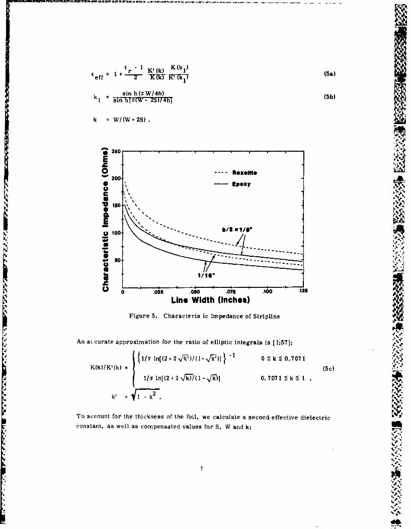
same substrate. Figure 8 shows a conctant impedance transition from CPW to
microstrip: at every point the combination of slot width and center conductor width
yields 50il. This was one of our experimental transitions-the center conductor
width at the narrow end is the same as that of 50 n coax.
4. EXPERIMENTS
4.1 Procedure.
The artwork for the circuits was drawn to 200 percent actual size on the
Calcomp plotter with a liquid ink pen. The photographic negative used in photo-
etching was shot to actual size. The artwork included the outline and hole pattern
for the test fixture, to make sure the circuit was aligned properly.
Figure 9 shows a microstripline mounted in the aluminum test fixture. The
SMA jack-tab connectors are mounted with screws on either end of the fixture,
with the tab soldered to the transmission line. Nylon screws are used to hold the
substrate flush with the aluminum fixture, which forms the ground plane.
All measurements were made using an HP8408 automatic network analver.
3. Rowe, D. A., and Lao, B. Y. (1983) Numerical analysis of shielded coplanarwaveguide, IEEE Trans. Microwave Theory Tech., MTT-31:911-915.
9

t er a2.4
soC
Ti
.02
.01 , ------
Slot Width, S (inch**)
FigLre 7. Characteristic Impedance of Grounded Coplanar WaveguideI4.2 Multiple Reflections and Reference P'lane Extension
typical measurement of return loss is shown in Figure 10a. The periodicity
is the effect of two mismatches in series, illustrated schematically in Figure l0b.flgure 10c relates that to the actual circuit being measured: Zand Z. are the
1 2discontinuities between the stripline an I the coaxial connectorq. The second
connector is terminated with a 50SI matched load, and we assuni-, that it has 7ero
reflection coefficient.
10
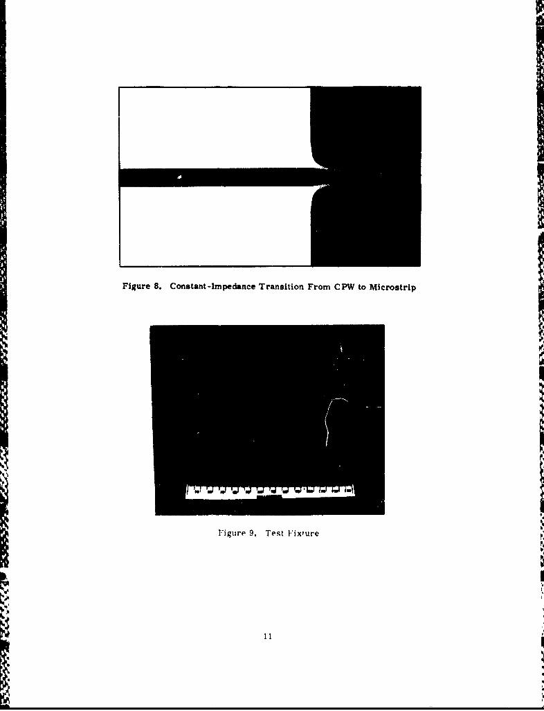
Figure 8. Constant -Impedance Transition From CPW to Microstrip
1--iure . Tet Vitur

m0m
Pro3 eeeo LOU.) As Ag As
(a)(b)
SAIM 00Ae atm P*.,M M o~
(a)
Figure 10. F eflection From Two DiscontinAities: (a) Measured ReturnLoss, (b) ScIematic Representation, and 4) Actual Circuit
The network analyzer injects a current I into the circuit and measures the
returning current Ir . The reflection coefficient is Pm• Iralip which is a sum of
all reflections in the circuit. We want to isolate p,. the reflection coefficient of
the first transition. Appendix A shows that the total reflection coefficient is:
Proa e'J2PI I p I + P2 I1-P2 1 2 e2a12 eJ2j 2 i2 ] (7)
(assuming the first section of coaxial line is lossless). The ineasured data from
Figure 10a is plotted in polar form in Figure IIa. Figure lIb shows the same data
with a phase correction of +20,1 " The result of that phase correction is that the
measured data describes a circle about some central point on the polar plot, as
shown in Figure 1lb. That point is the vector p,. The phase correction essentially
moved the reference plane to the position of the first discontinuity.
This reference plane extension technique allows us to clobarly identify p, in
both magnitude and phase. Figure 1 lb is a measurement made on a stripline thatwas too narrow due to overreduction during photographing, and also a slight over-etching.The resulting line width of 0.073 in. corresponds to an impedance of 56. 5A. The
venter of the best fit circle in Figure I lb has a resistance component of 1. 15 X 500,or 57. 5 Q.
12

1
'k. to j--S " *40
LI-4-
It.
CIS
0. 114,
13:

43 Muwmsns
4.3.1 MITERED MICROSTRIP
The mitered microstrip is a line of uniform width, except that near each con-nector, it is angled away from the connector's flange. as illustrated in Figure 12.
We tested several versions, each with a different angle of miter, a. The measuredreflection coefficients are shown in Figure 13. The 150 -mitered microstrip yields
the lowest reflection coefficient over the frequency range from 8 to 18 GHz. Evi-
dently, the slight miter of 150. just enough to get the corners of the line awayfrom the flange, reduces the stray inductance at the junction without changing Zo .
As the microstrip is mitered further, the characteristic impedance of the linenear the connection grows larger, resulting in a mismatch between it and the 50nconnector. We conclude that the best design of mitered microstrip transition is
the 150 taper, although we do not know if this will hold true for other dielectrics
and substrate thicknesses.
CoaxialComaeoter Flange
Miorostrip
Figure 12. Mitered MicrostripGeometry
4.3.2 STRIPLINE TO MICROSTRIP
We expected to have no problem in matching a 50S stripline to the SMAconnector because their dimensions are so similar. As Figure 14 shows, thereflection coefficient measured from the uniform stripline was slightly lower than
the best microstrip case (15° miter).
14

A
04e'
C 05la* o I*,i
-3
C* Q'Ar~
C/
0
8 10 12 14 16 I
Frequency (GHz)
' Figure 13. Measured Reflection Coefficient of MiteredMicrostrip Lines
The stripline-to-microstrip transition is shown in Figure 15. At the edge
of the fixture, the coax connector launches into a s~ction of 50SI stripline formed
by a narrow conductor covered by a rectangular piece of cooper-clad material.
The right side of the circuit is shown with the cover piece remroved. The transi-
tion is simply an abrupt truncation of the top ground plane of the stripline at the
point where the conductor widens to the width of 50SI microstripline. The results,
shown in Figure 16 were rather disappointing. It is evident that the transition from
the stripline to the microstrip introduces a very strong reflection. At some fre-
quencies. it appears that the circuit is radiating from those discontinuities, or
from the combination of the two discontinuities.
15

IA
i A U*Io.rn SripileeO
0 160 Mltored Ulorestrip
M41
C
0
S.2-
C0 0
00
8 0 12 14 1 ;
Frequency (GHz)
Figure 14. Stripline Reflection Coefficient
Figure 15. Stripline to Microstip Transition
16

E04
C
\
= 2
O .C40 00 0
0 0 \ II
S 1 12 14 16 Is
Frequency (GHz)
Figure 16. Measured Reflection CoefficientIStripline -Microstri p Transition
4.3.3 COPLANAR WAVEGUIDE TO MICROSTRIP
Figure 17 shows the mea,;ured reflection coefficient vs frequency fox' the
CPW-microstrip transition of Figure 8, compared with tha 150 -mitered micro-
strip. Although the CPW reflection coefficient is somewhat higher, the measured
data show only the two mismatches at each end of the circuit. We conclude that
the transition from CPW to microstrip can work properly, but there is a strong
reflection from the CPW-coax junction.
4.4 Ntirrostrip Dispersion **
NiCrostripline is a dispersive transmission medium because the velocity ofpropagation along the line varies with frequency. The reason this is so is that the
air' above the substrate, Effectively, the dielectric constant will appear to be
something in between that of air and that or the substrate's E r- As frequency
changes. so does the structure of the fringing fields, resulting in a change in
* 17I %I

A
00C
.2 0\/\0 / \
0
CI*'0 .1 1 2 Is
0 0
F Mz
gC
efetv dilcrccntn.Gpae4l4gietefloigepeso o h
U0
effective dielectric constant. Gupta etic awe givle the foloig exprengfthe
A g =A [ Eef~ 1:63 1:
gO
e2
Eeff~ (f = r ( r - eo)I[l+G(flfp)2 (8a)
where ce is as given in Eq. (3) and:
eoII
G =1 ?5760 +0.004 Z. (8b)
f (GHz) =15.F66 Z / h(mls) n(8c)p0
4. Gupta, K. C., Garg, R., and Chadha 4 R. (1981) Computer-Aided Design ofMicrowave Circuits, Artech House. Dedham, Masshuset ls.
18

For our parameters of W = 0. 17174 in.. h = 0.0625 in. = 62.5 mils, t = 0.0014 in.
(1 oz. copper clad), cr = 2.54 and Zo = 501, Eq. (8c) reduces to:
eff(f) = 2.54 - 0.417/[1 + 1.066(f/fp) 2 ] (9)
f = 12.528 GHzp
Figure 18 shows the Ceff(f) calculated from Eq. (8a) and the measured effective
dielectric constant, which was reduced from measured insertion phase data as
follows. The electrical length of the line is
Ie (10)e
where c is the speed of light and A0 is the change in insertion phase due to a change
Af in frequency. Knowing that the physical length cf the line is 1p 6. 000 in., we
calculate Eeff from:
-f (e/Ip)2 (11)eff
eff e p
The measured and calculated c eff in Figure 18 disagree by about 10 percent.
We believe the discrepancy is an inaccuracy in the formula for the effective dielectricconstant for DC, given by Eq. (3), since the shape of the two curves match quite
well, but seem to be offset.
5. CONCLUSIONS
Three types of printed circuit transmission lines have been investigated for
possible use in constructing transitions to coax cable from microstrip. The best
transition we found wasthe simplest: the microstrip with a tapered end, or 15, miter.
The stripline-to-microstrip transition had much higher reflection than even the
non-mitered microstrip, and hence does not offer any hope of a better transition.
The CPNV-microstrip transition seems to work properly, but the CPW itself is a
poor match to the coaxial connector.
19
b-S
'-S

I)
5 2.6 ,
Er
C
CALCULATEDC0
-MEiASURED
I I I I I I2 6 10 14 Is
Frequency (GHz)
Figure 18. Calculated and MeasuredEffective Dielectric Constant for 509Microstrip Line on Rexolite
In the course of these investigations, we have verified the design formulas
for characteristic impedance of the microstrip, stripline and grounded coplanar
waveguide. On the other hand. we have noted a disagreement with the published
theory of effective dielectric constant of microstrip, and some further experimenta-
tion with other substrate materials will be needed to resolve the dispute.
20

;Reflection From Two Discontinuities
When measuring'the reflection coefficient of acircuitwith two discontinuities,
suchas our printed-circuittransmissionflines, two phasors result. The situation
-is illustrated in Figure Al. The two discontinultiem are the ti-ansitions §frofn -the
coaxial test connectors to thetransmission line.. The second conhectbris ti'-
4minated with a matched load, so we assume'that there is no third reflection.
The measured reflection coefficient is Pi = I /, where I. is thecurrent intor1
the circuit and I is the total current reflected back out oftthe circuit, as observedr
by the network analyzer. Allowing for attenuation in the first length-of line (coax)
the-current into the first connection is:
1 exp[-jj3 l I ] exp[mal1] (AI)
Of the current that reaches the first connection, Ir I is reflected back toward the
source, which sees it phase shifted by twice the length of the first line section; and
tI goes on to the second connection:
I rl = I i e x p [ - ,12 l1 exp[-2alylI (A2a)
Iti = Iilll o1 ) • (A2b)
21

121
:Figur6 Al. A Transmission. Line-Circuit-'With twoDiscniutes-nSr,
Ir-2is the-, current -returning to the-first connector after traversig the 'test
'circuitandrefl1dti ng~fr6m-the -second&'c6nnectorv
I Iti 6kp[-;j?~ 2 0% t2~2 LI WA)
An amounit- 1(1#rl) mfakes itthroukh the first coniedtor on its wav'back.tathe generator. with th6 result that the, total, fe fle ctioni 'def ficient, ob~e rV6d is:
-2 r21 e 1 2 IiCa1 2 eJ (A4)2e (PI 'P2 -p 1 e ej j32 12
The combination of, thesetIwo phasors presents a problem in attenoting toeduce- the measured reflection data. 'A hepolar plot of Figure AMa shows,, As
we change freqiuenicy, 'both vectors are rotating (iince d;. is changink)aind theresultant conveys little information. On the. other hand, if'we know. I. then we can-remove the effect of the first, phasor simply by-adding 2g3~l, to the measured phase.
Neglecting the minor attenuation introduced'by the first connector,, E4, (A4)veduces to:
P p1 + ' pIP2 I ) 1 12 e 2 '' e-~3l (A 5)
Now, the measured data plotted in polar form is Figure AMb The phase repre-senting the second discontinuity is rotating about p,, which is fixed. We can thenaccurately determine both the magnitude and phase of p, by fitting a circle to the
measured data.
22

(a)
Figure A2. Polar Plot of Measured Reflection Coefficient vs Frequency:(a) Reference Plane at Measurement Plane and (b) Reference Plane atFirst Discontinuity
The physical length of the SMA coaxial connector (female, or "jack"), from
the flange to the very top is 0.375 inch. The coax region is recessed 0. 075 in.
below the top. The dielectric material is Tetrafluoroethylene with a dielectric
constant of about 2. 1. Thus, its electrical length is approximately 0. 435 inch.
23