power amplifier - rfic · p-15: a 2.4-ghz 0.18-um cmos self-biased cascode power amplifier two...
TRANSCRIPT

Power AmplifierLiterature Survey
SUCHITAV KHADANGA
RFIC TECHNOLOGIES, BANGALORE, INDIA
http://www.rficdesign.com

P-1: Design of a 2.4GHz Power Amplifier
Switch type power amplifier is the most important characteristic of high efficiency.
The efficiency of the switch amplifier in turn depends on the gate driving signal.
To achieve a suitable gate signal two pseudo E class drivers are implemented.
Limited DC RF choke inductance is used.
Due to large inductances in this circuit a bond wire is used for testing.
Supplies high power combined with proper working of power stage at the respective states.
Consists of Class F-amplifier, inverter and Class E drivers.

Technical Details P-1
SPECIFICATIONS VALUE
•Technology •TSMC 180nm
•Supply Voltage •1V
•Saturate Output Power •5-8dBm
•Frequency Operation •2.4GHz
•Input power •-10dBm
•PAE •19%
•S11 •<-23dB
•S22 •<-9dB
•Topology •Differential
•Year of Publication •2013

P-2: A Digitally Modulated Class-E Polar Amplifier in 90 nmCMOS
Class E amplifier with Digital impedance amplitude modulation.
Suitable for moderate PAPR(Peak-to-average-power-ratio) modulation schemes (π/4 DQPSK).
Digitally tuneable matching circuit used to perform AM and hence non-linearity is reduced.
Peaks of both current and voltage do not overlap, minimizes power dissipation.
Π-type network is chosen as it covers entire Smith chart.
Net die area reduction.
Increase in Bandwidth as phase and amplitude take different paths.
Passive network simple in construction.

Technical Details P-2
• Technology
• Supply Voltage
• Output Power
• Small Signal Gain
• Frequency operation
• Efficiency
• EVM
• Die-Area
• Topology
• Year of Publication
• CMOS 90nm
• 1.2V
• 9dBm
• 11dB
• 2.4GHz
• 30%
• 2.6%
• 0.924 mm2
• Single Ended
• 2012

Circuit (a) suffers from high power consumption, large output swings at drain of M2, bias current must be high.
Stacking of circuits (b) is done to mitigate drawbacks of (a).
Advantageous as it reduces power consumption and also protects M2 from excessive drain-gate voltage.
Dual band PA.
Cascoding with power stage and driver to increase linearity.
P-3: A Low-Power 2.4GHz Transmitter/Receiver CMOS IC

Technical Details P-3
SPECIFICATIONS
• Technology
• Supply Voltage
• Output Power
• Frequency Operation
• Output Power consumption
• Bias current
• Load impedance
• Die-Area
• Topology
• Year of Publication
VALUE
• CMOS 0.25µm
• 2.5V
• 0dBm
• 2.4GHz
• 16mW
• 3mA
• 50Ω
• 1.83mm X 2mm
• Single Ended
• 2003

P-4: Optimised high-efficiency Class E radio frequency poweramplifier for wide bandwidth and high harmonics suppression
Switch Mode Class-E PA Single ended
Wide Bandwidth
Combine Parallel Circuit Load
High-Order Harmonic Suppression (single reactance compensation technique with harmonic trap at load)
Inductive at fundamental frequencies and Capacitive at harmonic frequencies
Combining power technique (high eff and PAE)
Less Area and Less Cost
Stability and Robustness has been verified

Technical Details P-4
SPECIFICATIONS
• Technology
• Supply Voltage
• Output Power
• Frequency Operation
• Efficiency
• Second Harmonic
• Stability (10:1 VSWR)
• Robustness (10:1 VSWR)
• Drain Efficiency
• Topology
• Year of Publication
VALUE
• LDMOS
• 7.2V
• 6.5-7W
• 136-174MHz
• >60%
• 84dBc
• Stable
• NO degradation
• 71%
• Single Ended
• 2013

P-5:A 2.4 GHz 0.18-μm CMOS Class E Single-Ended PowerAmplifier without Spiral Inductors
Class-E PA Single ended.
Bond Wire-High Q-Less area-Increased performance.
Cascode with self-biasing to overcome device stress.
Two Stages: Driver stage (Class-A)
Power stage (Class-E)
Output power changes approximately proportional to Vdd²,
No Baluns-reduce chip area

Technical Details P-5
SPECIFICATIONS
• Technology
• Supply Voltage
• Output Power
• Frequency Operation
• PAE
• Chip Sizes
• Topology
• Year of Publication
VALUE
• TSMC CMOS 0.18µm
• 3.3V
• 19.2dBm
• 2.35-2.45GHz
• 27.8%
• 0.37mm2
• Single-Ended
• 2010

P-6: Design of Efficient Class-E Power Amplifiers forShort-Distance Communications
Class-E with π-matching.
Pre-driver and power stage to boost the power.
PE and PAE nearly the same.

Technical Details P-6
SPECIFICATIONS
• Technology
• Supply Voltage
• Output Power
• Frequency Operation
• Maximum Overall Efficiency
• Power Gain
• Output Impedance
• Second Harmonic
• Third Harmonic
• Chip area
• Topology
• Year of Publication
VALUE
• CMOS 0.13µm
• 0.45-0.8V
• 3.2-5.7dBm
• 2.4GHz(2.2-2.5GHz)
• 55%
• 20dB
• 50Ω
• -25.5dBc
• -41dBc
• 0.5mm2
• Single Ended
• 2012

P-7: A Dual-Band CMOS Power Amplifier at 1.8 GHz and2.6 GHz for LTE Applications
Dual band-PA (1.8 & 2.6GHz)
Two stage cascade structure
Driver stage
Power stage
The driver stage uses a RC and resistive feedback-increased BW
The power stage employs diode linearizer-linearity
Cascade structure-low breakdown voltage-good input-output isolation-high power gain
RC-stability of power stage-improve linearity

Technical Details P-7
SPECIFICATIONS
• Technology
• Supply Voltage
• Output Power
• Frequency Operation
• PAE
• Power Gain
• Output Impedance
• Input return loss
• Output return loss
• Power Consumption
• Topology
• Year of Publication
VALUE
• TSMC CMOS 0.18µm
• 3.3V
• 24.6/23.4dBm
• 1.8/2.6GHz
• 34.6/40.5%
• 22/20.2dB
• 50Ω
• <-18dB
• <-8dB
• 211mW
• Single Ended
• 2012

P-8: A Broadband Injection-Locking Class-E Power Amplifier
Two stage Injection locking Class-E PA
PA-oscillator-output voltage tuned to input frequency
High PAE and Power Gain
GMSK and 64QAM
Two stage cascade structure
Driver stage
Power stage
Negative resistance concept to compensate the losses
Auxiliary generator is used for stability analysis
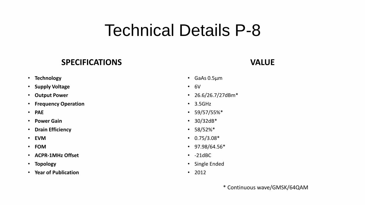
Technical Details P-8
SPECIFICATIONS
• Technology
• Supply Voltage
• Output Power
• Frequency Operation
• PAE
• Power Gain
• Drain Efficiency
• EVM
• FOM
• ACPR-1MHz Offset
• Topology
• Year of Publication
VALUE
• GaAs 0.5µm
• 6V
• 26.6/26.7/27dBm*
• 3.5GHz
• 59/57/55%*
• 30/32dB*
• 58/52%*
• 0.75/3.08*
• 97.98/64.56*
• -21dBC
• Single Ended
• 2012
* Continuous wave/GMSK/64QAM

P-9: A 60 GHz Drain-Source Neutralized Wideband Linear Power Amplifier in 28 nm CMOS
Drain-Source Neutralization-stability of PA-wideband, by low-k transformer
Three stage cascade structure using transformers
Pre-Driver stage
Two Cascode Power stage
Power Combiner
Employ DAT for higher output power
Q-current is halved for same output power by using cascode

Technical Details P-9
SPECIFICATIONS
• Technology
• Supply Voltage
• Saturated Output Power
• P1-db
• Frequency Operation
• PAE
• Power Gain
• Bandwidth
• Power Consumption
• Chip Area(core/total)
• Topology
• Year of Publication
VALUE
• CMOS 0.028µm
• 1.8-2.1V
• 16.5dBm
• 11.7dBm (62GHz with 6.3% PAE)
• 60GHz
• 12.6%
• 24.4dB
• 11GHz
• 211mW
• 0.122/0.64mm2
• Differential
• 2014
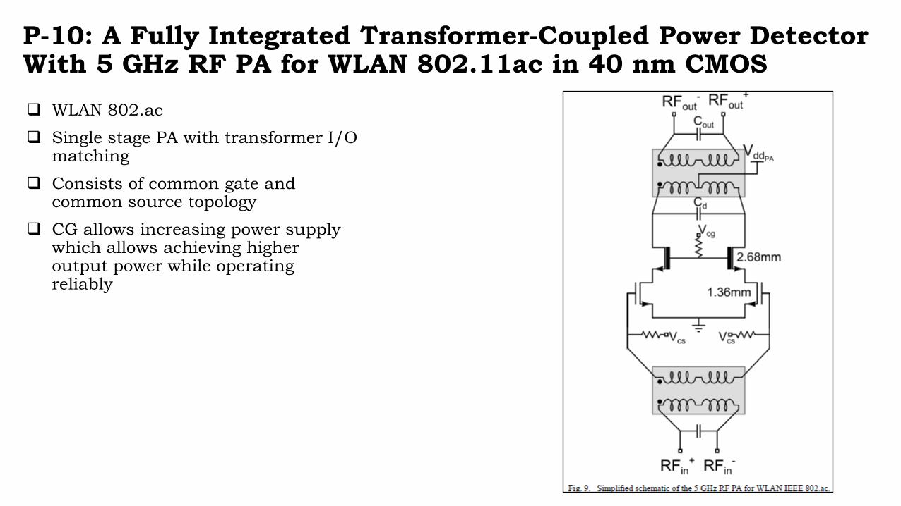
P-10: A Fully Integrated Transformer-Coupled Power Detector With 5 GHz RF PA for WLAN 802.11ac in 40 nm CMOS
WLAN 802.ac
Single stage PA with transformer I/O matching
Consists of common gate and common source topology
CG allows increasing power supply which allows achieving higher output power while operating reliably

Technical Details P-10
SPECIFICATIONS
• Technology
• Supply Voltage
• Saturated Output Power
• Output Power
• Frequency Operation
• PAE
• Power Gain
• Output Impedance
• Peak Drain Efficiency
• Topology
• Year of Publication
VALUE
• TSMC CMOS 0.040µm
• 2.5V
• 22.9dBm
• 24dBm
• 4.5-5.5GHz
• 38.8%
• 10dB
• 50Ω
• 40.8%
• Differential
• 2015

P-11: A CMOS High Efficiency +22 dBm Linear PowerAmplifier
Parallel A&B PA
Improves dynamic range and powerefficiency
Increase P1dB by 3dB and reducespower consumption by 50% in thelinear operation range
Class A amplifier is the primarycontributor for gain at the low signallevels, however class B at the highsignal levels.
Shunt inductors Lin are used to
match the inputs, and the inductors
RFC are used as RF chokes to
prevent coupling of the RF signal to
the power supplies and inductors Lo
is used to match the output port.
Fig:-Conceptual block diagram of parallel A&B amplifier

Technical Details P-11
SPECIFICATIONS
• Technology
• Output Power
• PAE
• Linear Power Gain
• P1dB
• Year of Publication
VALUE
• CMOS
• 22dBm
• >40%
• 12dB
• 20.5dBm
• 2003

P-12: Design of CMOS Class-E Power Amplifier for WLAN andBluetooth Applications
Class-E PA with modified driver
Better output power at minimum input power levels
Negative capacitance to reduce parasitic capacitance without external circuitry
Better power gain at cost of extra hardware
Fig:- single ended
class E PA
Fig:-Parallel PA

Technical Details P-12
SPECIFICATIONS
• Technology
• Supply Voltage
• Gain
• Frequency Operation
• PAE
• Topology
• Year of Publication
VALUE
• UMC CMOS
• 1.8V
• 20dBm
• 2.4GHz
• 40%
• Single ended
• 2012

P-13: Low-Power RF Transceiver for IEEE 802.15.4 (ZigBee)Standard Applications
Two stage PA
Low power
Consists of class A pre-amplifier that drives the high efficient class C amplifier.
Class C amplifier has been designed with conduction angle of 150 degrees, which allowed to achieve good tradeoff between efficiency and gain.
The PA can provide an output power up to of 6 dBm when it is driven with an input power of -15 dBmsupplied by the class-A driver stage.

Technical Details P-13
SPECIFICATIONS
• Technology
• Supply Voltage
• Output Power
• Saturated output power
• Power Consumption
• Topology
• Year of Publication
VALUE
• BiCMOS
• 1.8V
• 6dBm
• 8dBm
• 16mW
• Single Ended
• 2006

P-14: A Highly Linear and Efficient CMOS RF Power Amplifier With a 2-D Circuit Synthesis Technique
Class A tanh cascode cell(TCC) amplifier
Linearization with 2DCST over wide range
Doesn't require inverse circuit for amplitude correction
TCC is used to realize class AB amplifier having tanh-like current voltage characteristic
The total current is the linear sum of cell currents
Linearity can be synthesized by appropriate sizing and scaling of the current-voltage transfer characteristic of individual cell
Fig:-TCC CMOS RF PA
Fig:- TCC amplifier

Technical Details P-14
SPECIFICATIONS
• Technology
• Output Power
• Efficiency
• Topology
• Year of Publication
VALUE
• CMOS
• 24.9dBm
• 41.6%
• Single Ended
• 2012

P-15: A 2.4-GHz 0.18-um CMOS Self-Biased Cascode Power Amplifier
Two stage self biased cascode PA
Equivalent total gain is of three stages
Self biased cascoding reduces maximum drain-gate voltage across each transistor.
Input and Output matching are designed to be off- chip to increase matching flexibility and avoid excessive power loss of on- chip inductors
Traces on the PCB are used as transmission lines as a part of input, inter-stage and output matching networks(TL1-TL7)
A two step matching network is used to transform load to optimum load, composed of TL4-TL7 and parallel capacitors C3 & C4 , which short circuit the second and third harmonics to ground
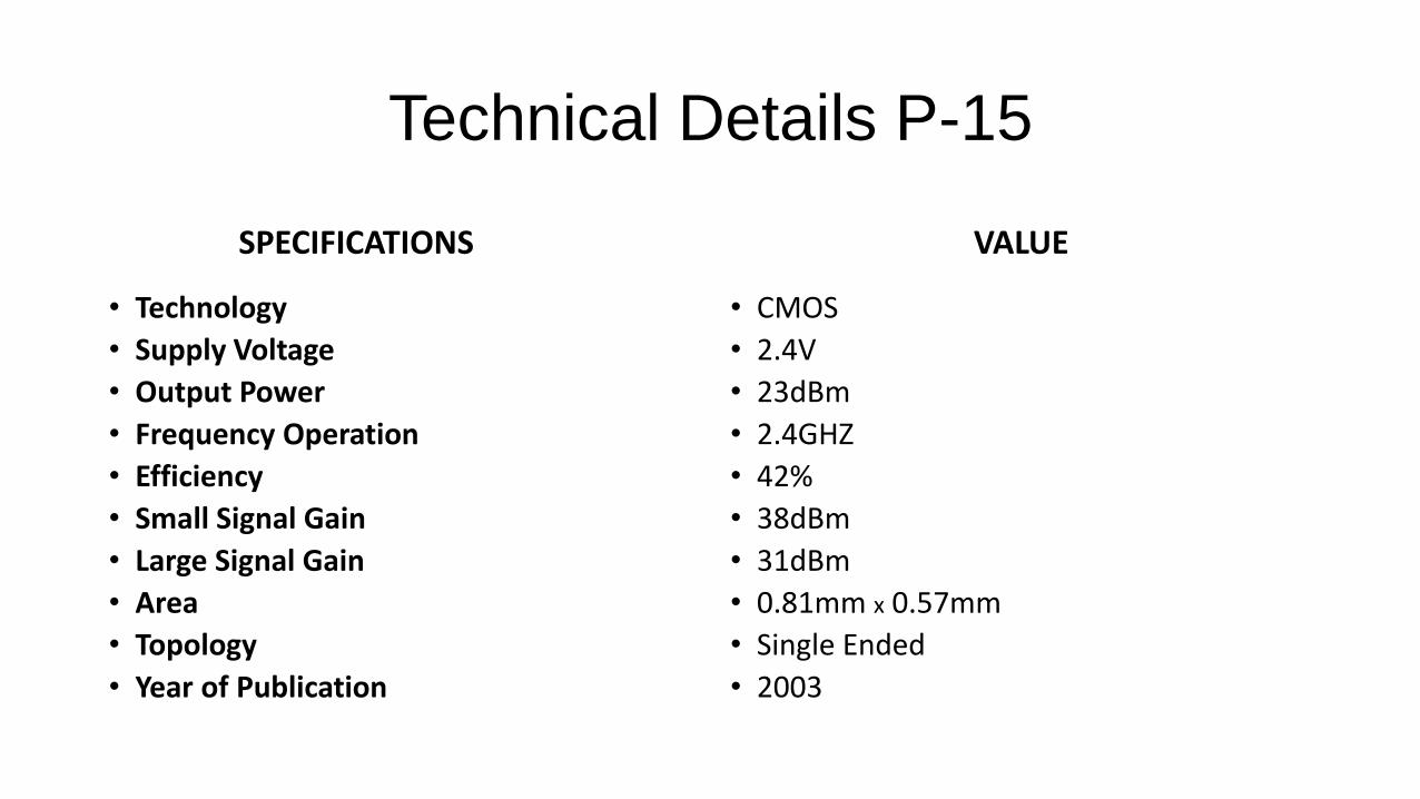
Technical Details P-15
SPECIFICATIONS
• Technology
• Supply Voltage
• Output Power
• Frequency Operation
• Efficiency
• Small Signal Gain
• Large Signal Gain
• Area
• Topology
• Year of Publication
VALUE
• CMOS
• 2.4V
• 23dBm
• 2.4GHZ
• 42%
• 38dBm
• 31dBm
• 0.81mm x 0.57mm
• Single Ended
• 2003