fast-settling low-power two-stage self-biased cmos ... fileself-biased cmos amplifier using...
TRANSCRIPT
Fast-Settling Low-Power Two-Stage Self-Biased CMOS Amplifier Using
Feedforward-Regulated Cascode Devices
Edinei Santin, Michael Figueiredo, Rui Santos-Tavares, João Goes, and Luís Oliveira
Department of Electrical EngineeringUniversidade Nova de Lisboa, Portugal
2
Outline
Introduction and MotivationProposed Amplifier
Description and Analysis
Circuit Design and OptimizationSimulation ResultsConclusions
3
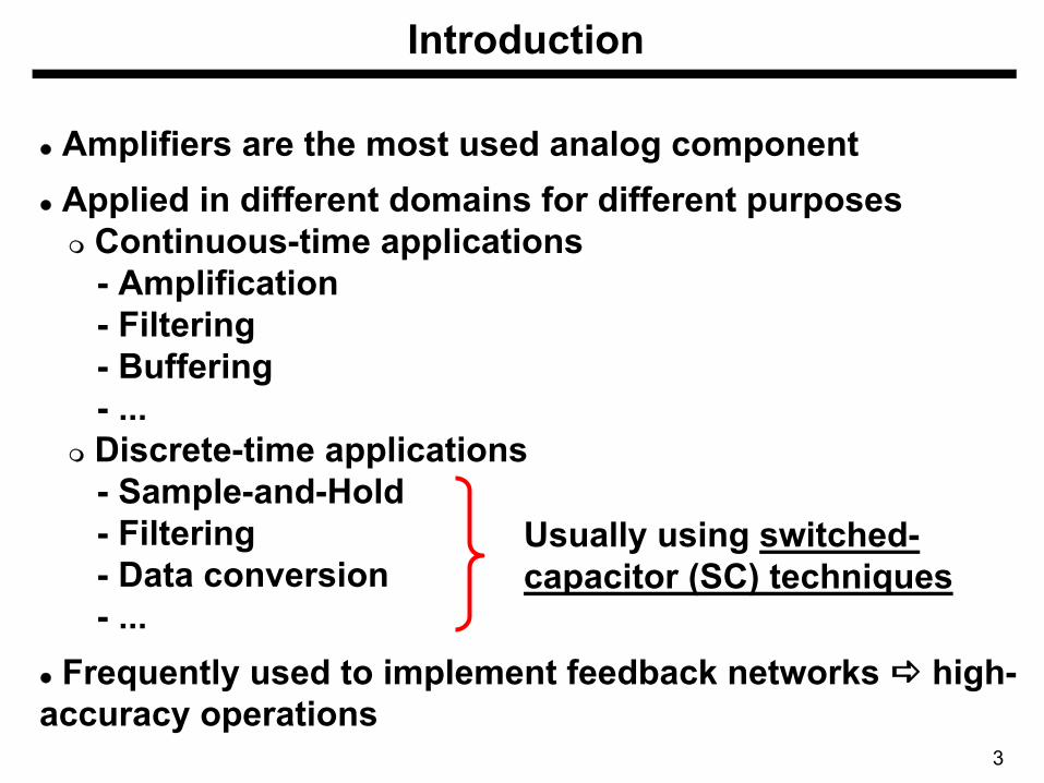
Introduction
Amplifiers are the most used analog componentApplied in different domains for different purposes
Continuous-time applications- Amplification- Filtering- Buffering- ...Discrete-time applications- Sample-and-Hold- Filtering- Data conversion- ...
Frequently used to implement feedback networks high-accuracy operations
Usually using switched-capacitor (SC) techniques
4
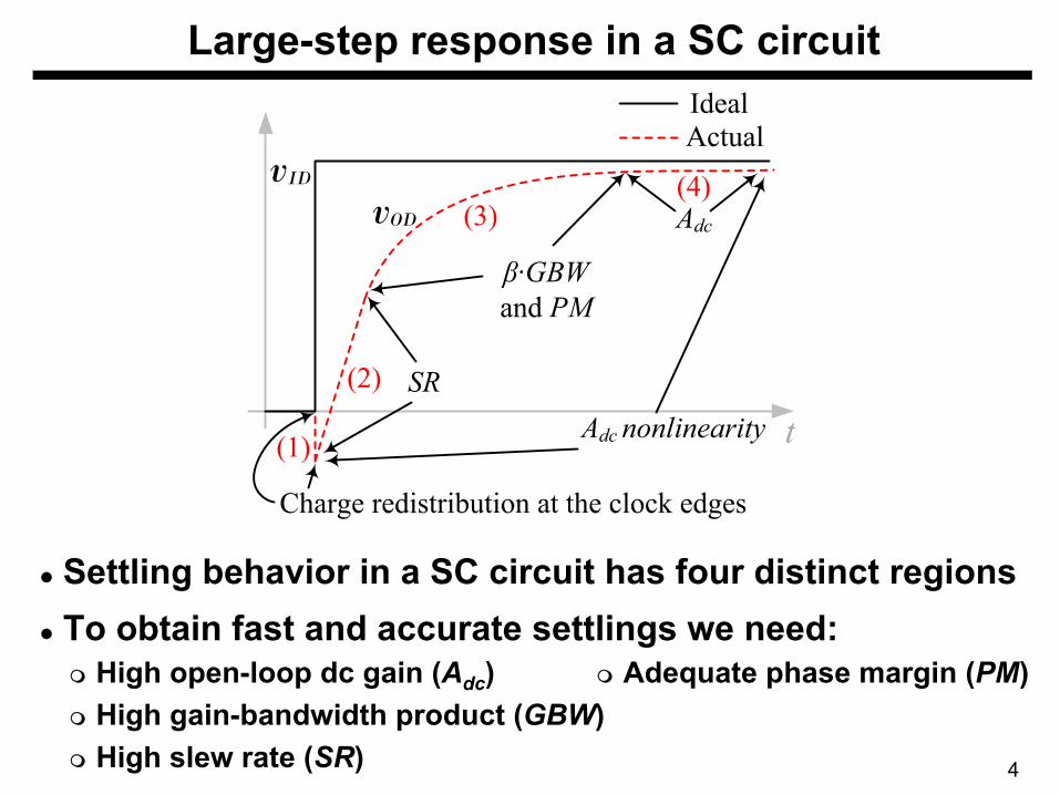
Large-step response in a SC circuit
Settling behavior in a SC circuit has four distinct regionsTo obtain fast and accurate settlings we need:
High open-loop dc gain (Adc)High gain-bandwidth product (GBW)High slew rate (SR)
Adequate phase margin (PM)
SR
β·GBWPM
Adc
Adc nonlinearity
vODvID
t
5
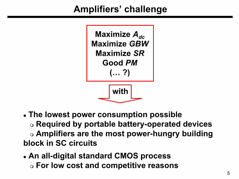
Amplifiers’ challenge
The lowest power consumption possibleRequired by portable battery-operated devicesAmplifiers are the most power-hungry building
block in SC circuitsAn all-digital standard CMOS process
For low cost and competitive reasons
Maximize AdcMaximize GBWMaximize SR
Good PM(… ?)
with
6
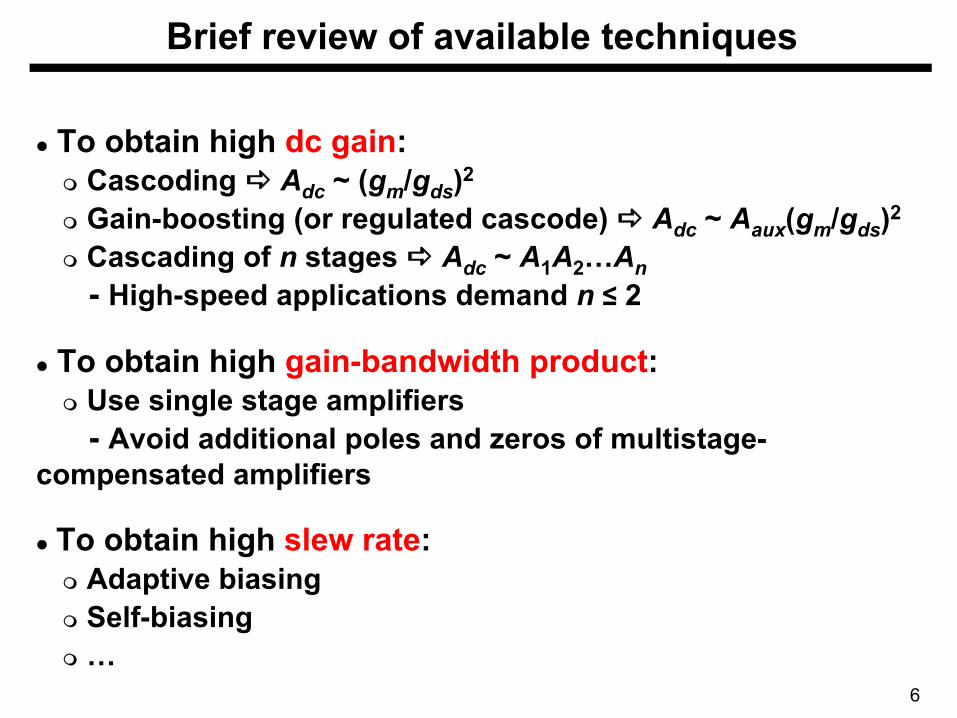
Brief review of available techniques
To obtain high dc gain:Cascoding Adc ~ (gm/gds)2
Gain-boosting (or regulated cascode) Adc ~ Aaux(gm/gds)2
Cascading of n stages Adc ~ A1A2…An- High-speed applications demand n ≤ 2
To obtain high gain-bandwidth product:Use single stage amplifiers- Avoid additional poles and zeros of multistage-
compensated amplifiers
To obtain high slew rate:Adaptive biasingSelf-biasing…
7
Outline
Introduction and MotivationProposed Amplifier
Description and Analysis
Circuit Design and OptimizationSimulation ResultsConclusions
8
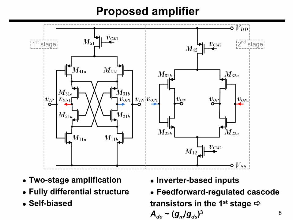
Proposed amplifier
Two-stage amplificationFully differential structureSelf-biased
Inverter-based inputsFeedforward-regulated cascode
transistors in the 1st stage Adc ~ (gm/gds)3
vIN
M11a
vIP vOP1vON1
M11b
M21a M21b
M31a M31b
M41a M41b
M51vCM1
VDD
M22b
vOP1 vON1vOPvON
M22a
M32b M32a
M42
VSS
M12vCM2
vCM21st stage 2nd stage
9
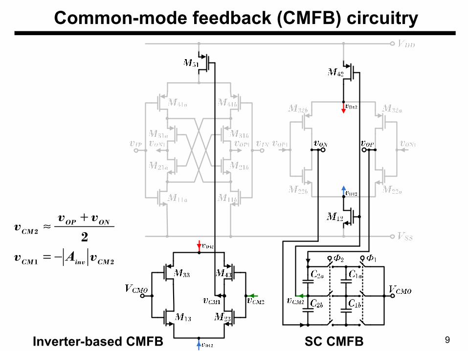
Common-mode feedback (CMFB) circuitry
Inverter-based CMFB SC CMFB
21
2 2
CMinvCM
ONOPCM
vAv
vvv
−=
+≈

10
Amplifier’s compensation (I)
Miller compensation 2 real poles
Small-signal differential-mode half circuit
Case IPoleZero
11
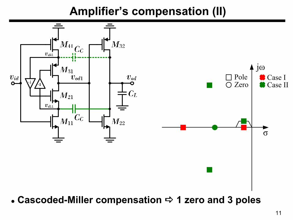
Amplifier’s compensation (II)
Cascoded-Miller compensation 1 zero and 3 poles
Case ICase II
PoleZero
12
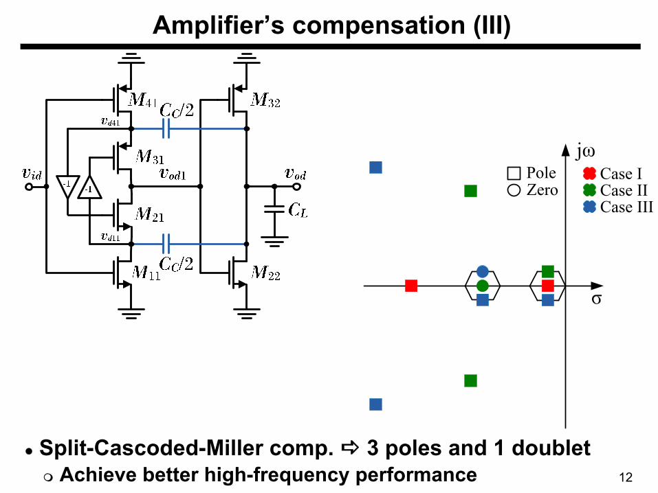
Amplifier’s compensation (III)
Split-Cascoded-Miller comp. 3 poles and 1 doubletAchieve better high-frequency performance
Case ICase IICase III
PoleZero
13
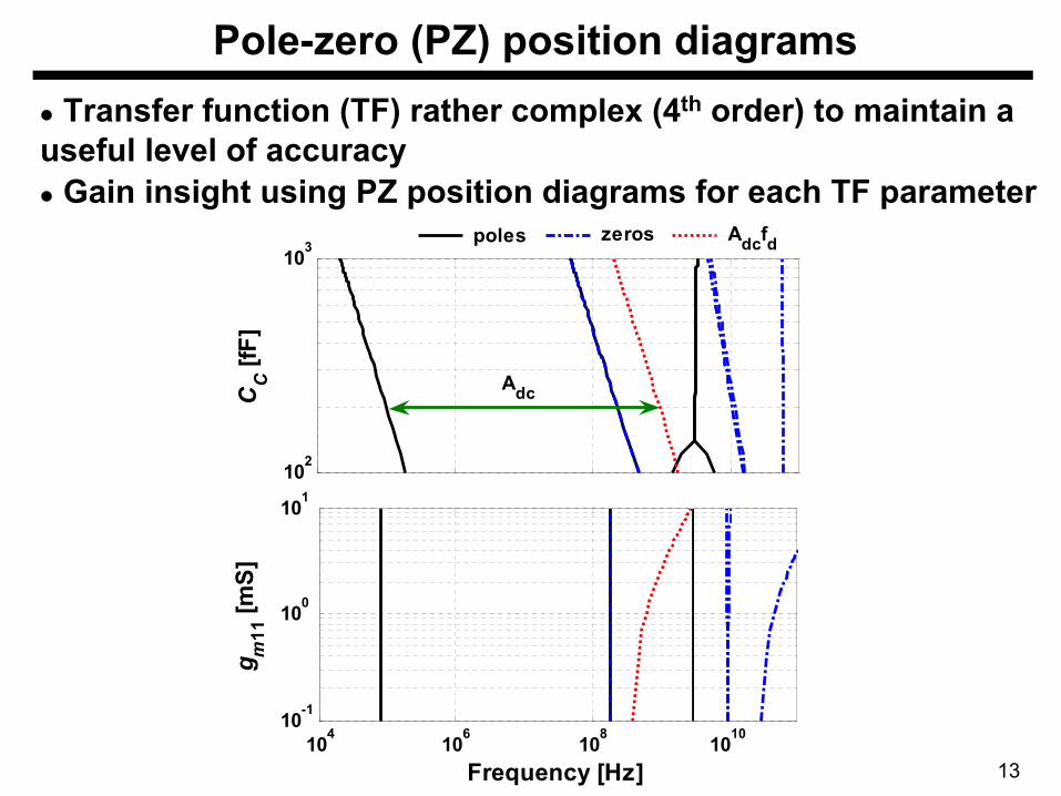
Pole-zero (PZ) position diagramsTransfer function (TF) rather complex (4th order) to maintain a
useful level of accuracyGain insight using PZ position diagrams for each TF parameter
102
103C
C [f
F]
104 106 108 101010-1
100
101
Frequency [Hz]
g m11
[mS]
poles zeros Adcfd
Adc
14
Outline
Introduction and MotivationProposed Amplifier
Description and Analysis
Circuit Design and OptimizationSimulation ResultsConclusions
15
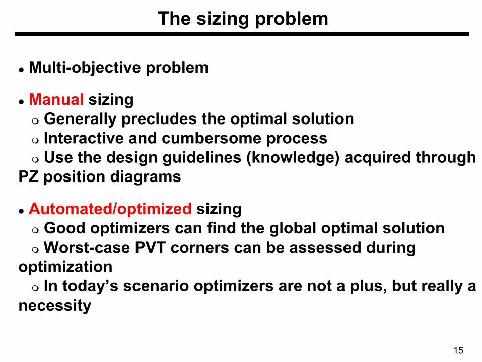
The sizing problem
Multi-objective problem
Manual sizingGenerally precludes the optimal solutionInteractive and cumbersome processUse the design guidelines (knowledge) acquired through
PZ position diagrams
Automated/optimized sizingGood optimizers can find the global optimal solutionWorst-case PVT corners can be assessed during
optimizationIn today’s scenario optimizers are not a plus, but really a
necessity
16
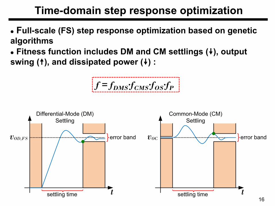
Time-domain step response optimization
Full-scale (FS) step response optimization based on genetic algorithms
Fitness function includes DM and CM settlings ( ), output swing ( ), and dissipated power ( ) :
vOD,FS
t
error band
settling time
vOC
t
error band
settling time
Differential-Mode (DM)Settling
Common-Mode (CM)Settling
f = fDMS·fCMS·fOS·fP
17
Outline
Introduction and MotivationProposed Amplifier
Description and Analysis
Circuit Design and OptimizationSimulation ResultsConclusions
18
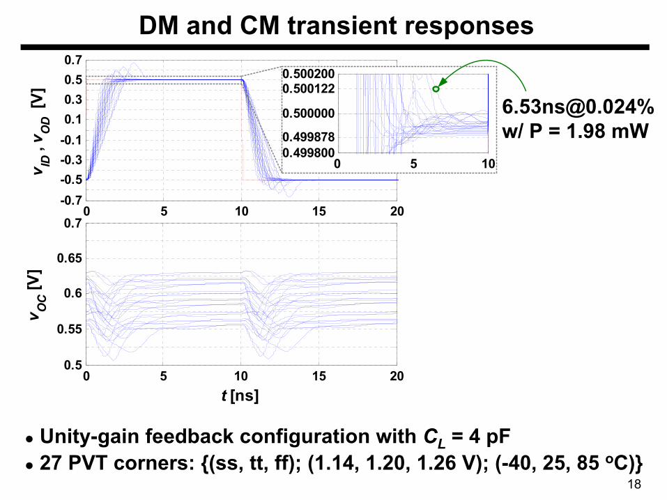
DM and CM transient responses
Unity-gain feedback configuration with CL = 4 pF27 PVT corners: {(ss, tt, ff); (1.14, 1.20, 1.26 V); (-40, 25, 85 oC)}
0 5 10 15 20-0.7-0.5-0.3-0.10.10.30.50.7
t [ns]
v ID ,
v OD
[V]
0 5 100.4998000.499878
0.500000
0.5001220.500200
0 5 10 15 200.5
0.55
0.6
0.65
0.7
t [ns]
v OC
[V]
[email protected]%w/ P = 1.98 mW
19
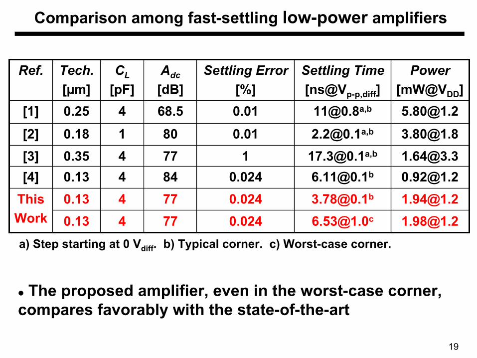
Comparison among fast-settling low-power amplifiers
The proposed amplifier, even in the worst-case corner, compares favorably with the state-of-the-art
[email protected]@[email protected]@0.1b0.0247740.13This
Work
[email protected]@0.1b0.0248440.13[4][email protected]@0.1a,b17740.35[3][email protected]@0.1a,b0.018010.18[2][email protected]@0.8a,b0.0168.540.25[1]
Power[mW@VDD]
Settling Time[ns@Vp-p,diff]
Settling Error[%]
Adc
[dB]CL
[pF]Tech.[µm]
Ref.
a) Step starting at 0 Vdiff. b) Typical corner. c) Worst-case corner.
20
Outline
Introduction and MotivationProposed Amplifier
Description and Analysis
Circuit Design and OptimizationSimulation ResultsConclusions
21
Conclusions
A fast-settling and low-power amplifier for switched-capacitor applications is proposed
The amplifier achieves outstanding performance by combining:
Self-biasingTwo-stage amplification with feedforward-regulated
cascode transistors in the first stageInverter-based fully differential structureOptimized compensation schemeTime-domain step response optimization for sizing

22
Acknowledgment
Portuguese Foundation for Science and Technology for funding

23
Thank you for your attention!
24
References
[1] M. Yavari and O. Shoaei, “Very Low-Voltage, Low-Power and Fast-Settling OTA for Switched-Capacitor Applications,” Proc. Int. Conf. Microelectronics, 2002.
[2] M. M. Ahmadi, “A New Modeling and Optimization of Gain-Boosted Cascode Amplifier for High-Speed and Low-Voltage Applications,”IEEE Trans. Circuits Syst. II, 2006.
[3] F. A. Amoroso et al., “Design Considerations for Fast-Settling Two-Stage Miller-Compensated Operational Amplifiers,” Proc. IEEE Int. Conf. Electronics, Circuits, and Systems, 2009.
[4] M. Figueiredo et al., “Two-Stage Fully-Differential Inverter-based Self-Biased CMOS Amplifier with High Efficiency,” Proc. IEEE Int. Symp. Circuits Syst., 2010.
25
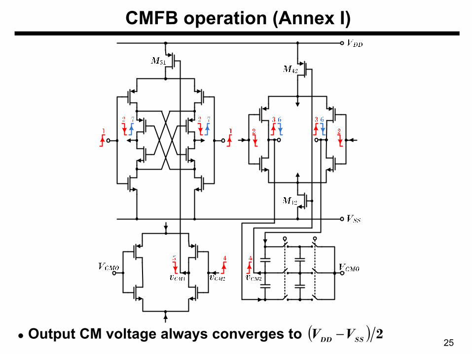
CMFB operation (Annex I)
Output CM voltage always converges to ( ) 2SSDD VV −