phase vi final submission - stevens institute of … · footstep and piezo strips. ... at the ultra...
TRANSCRIPT

ME 424 ENGINEERING DESIGN VIII
PHASE VI – FINAL SUBMISSION
PIEZOELECTRIC-BASED APPLICATION DEVELOPMENT
A SENIOR REPORT
GROUP 11: JIM WATERMAN ERIC MCCORMICK SCOTT HAMILTON SHINGO MATSUBARA DAVID MANNING
ADVISOR Frank Fisher
STEVENS INSTITUTE OF TECHNOLOGY Castle Point on Hudson
Hoboken, NJ 07030
May 1, 2008

Abstract The following report contains official documentation for Mechanical Engineering Senior Design Group 11, Piezoelectric-based Energy Harvesting. Contained within this report is a comprehensive design and analysis of a new product: a piezoelectric based energy scavenging floor tile that harvests energy from foot strikes and sends wireless signals for building surveillance purposes. The design will utilize ZigBee wireless transmission for communication between the tile and a remote computer. The tile will work in two different ways. During times in which security monitoring is not needed and people will be walking on the floor continuously, the tile will harvest the energy created by the piezoelectric strips. When being used as a security sensor, any step on the tile will create energy that is sent to a microprocessor and the microprocessor will send a short message to the remote computer noting that there was movement in the floor. This report includes the development, implementation, and tests conducted in the design of the prototype of the floor tile. The group was successfully able to harvest enough energy using piezoelectric materials in the floor tile to power a microprocessor and send a signal.
Executive Summary Piezoelectric Energy Harvesting is an emerging technology with many new and exciting applications. This project was undertaken using a particularly innovative technological breakthrough in this field from a company called Advanced Cerametrics (ACI) out of Lambertville, NJ. They have developed flexible piezo composites that generate nearly ten times the power of traditional ceramic piezos through the use of PZT fibers that exhibit the piezoelectric effect. This project utilizes the direct piezo effect, which converts mechanical to electrical energy, aptly entitled Energy Harvesting. Armed with this technology a design team of five mechanical and four electrical engineers took on the challenge of developing a unique application using this emerging technology. Several concepts were considered including a medical device, a game or toy, a sensing/monitoring application, a buoy light or ocean/wave application, or a sports device. However, after significant deliberation, a design comparison matrix, and the consultation of ACI, all of these applications were eliminated due to complexity and/or unfeasibility. The team considered it a better approach to take on a smaller scope and develop a complete and working prototype than to take on too much and develop a disjointed project. As such, the final chosen application was chosen as an energy scavenging floor tile system. With the plethora of wasted impact energy and the relatively simplistic design scope of a floor system, our Stevens advisors and our company sponsor ACI were supportive of our choice. As a corollary objective we decided to use the harvested energy for a useful purpose, namely, to serve as a
2

surveillance device that outputs wireless signals exclusively from its natively generated energy source. The initial conceptual approach involved a floor tile mounted on a foam subfloor, as explained in Section 2 of this report. The idea was that the piezoelectric strips would be hard mounted inside the tile, and that the whole tile would displace on the foam subfloor. Point masses were mounted on the piezo strips. As the tile displaced a differential inertia was exerted on the strips because of the point masses, causing the strips to vibrate and hence for energy to be generated. However, testing revealed that only negligible amounts of energy was generated in this manner. There simply was not enough energy transfer between the footstep and piezo strips. Additionally, the large point masses required caused the strips to vibrate at very low frequencies. Since the piezo strips generate max power at their resonant frequency, this was undesirable. As such, the team took on a new approach as explained in Section 3 of this report. In order to maximize energy transfer, a spring loaded actuation system was designed to physically actuate the strips in lieu of a foam subfloor. The physical actuation eliminates the frequency issue by vibrating the strips at their natural frequency. The system also allowed the strip to be vibrated twice per footstep, once on the down stroke and once on the upstroke. The superior advantage of this system was immediately apparent as voltage output from the strips was orders of magnitude better. Concurrent to this development were several changes in the system’s electrical components. The first attempt at creating an energy harvesting circuit involved the use of a transformer, a homemade rectifier using four diodes, some resistors and a 1F capacitor. Several iterations of this circuit were attempted, but only with minimally favorable results. At best, the most favorable homemade circuit was 5% efficient, thus nullifying most of the energy generated through foot strikes on the tile. At the ultra low power levels of the piezo strips the circuit components were simply not applicable. As such, through the consultation of ACI, a commercially available Energy Harvesting Circuit model EH301 was purchased from a company called Advanced Linear Devices. A PCB with a footprint of an AA battery, it offered a much more elegant and simple means of storing energy. The device was specially designed to handle a variety of input voltage spikes and both store and retain small amounts of energy with great efficiency. Testing with a singular piezoelectric strip revealed an efficiency of roughly 90%, orders of magnitude better than home grown attempts. The electrical system of this project is summarized in Section 4 of this report. After several iterations of the actuation system to optimize its performance, the mechanical and electrical systems were integrated and testing was performed. The Testing and Results are more completely documented in Section 5 of this
3

report. Four piezoelectric strips were mounted in the floor tile and connected to the Energy Harvesting Circuit to maximize energy output. A multimeter was used to measure the voltage stored in the capacitor bank of the energy harvesting circuit. Several test variables were used and iterated upon in order to optimize the energy generating capability. The results revealed that only 20 footsteps were required to generate 8.3mJ of useful power. An ultra low power Zigbee wireless system was used with an energy requirement of approximately 1.44mJ per wireless signal. Therefore in just 20 footsteps the floor tile generated enough power to send 5 wireless signals. Having shown the system’s energy generating feasibility, the main issue of this project involved directing this energy to send a wireless signal. The approach was to power a microcontroller with the Energy Harvesting Circuit output. Then, the microcontroller would execute a program to create the correct output signal (USART) to power the Zigbee transmitter. This signal was regulated to the correct voltage using a voltage divider to power the Zigbee wireless transmitter. The powering of the microcontroller was successfully demonstrated, as was the performance of the wireless transmitter. However, due to time constraints, the linkage between the two was unable to be achieved, as is explained in Section 4 of this report. Except for this small electrical issue, the project achieved its desired result. The application performance has the promise of serving many other uses in addition to its surveillance application. These including motion monitoring throughout buildings, the location monitoring of vehicles, light proximity sensors or any other application that requires energy input on the order of 8.3mJ or below. Several suggestions to improve the design of this system, as well as a more complete list of alternate uses and recommendations for piezoelectric development are summarized in Section 6 of this report.
4

Acknowledgements Mechanical Engineering Design Team: Jim Waterman, Eric McCormick, Scott Hamilton, David Manning, Shingo Matsubara Electrical Engineering Design Team: Neil Patel, Michael Ivey, Mark Vizthum, Arturo Dizon Advisors: Professor of Mechanical Engineering Frank Fisher Professor of Electrical Engineering Bruce McNair Stevens Institute of Technology Machine Shop George and Bruce Advanced Cerametrics Company: Bud Cass - Advanced Cerametrics Co. President Farhad Mohammadi – Advanced Cerametrics Co. R&D Director Dr. Kim – Advanced Cerametrics Electrical Expert Traditional ceramic piezoelectric materials are very brittle, and have low electrical energy outputs per unit strain. Materials research and technology improvements have changed the perspective entirely, and the application of piezoelectrics to a multitude of new applications is becoming an achievable possibility in light of these technological breakthroughs. Some examples include active smart sporting goods, next generation aircraft, automobiles, motorcycles, wireless sensors, acoustical equipment, sports gear, industrial equipment, infrastructure, apparel and more. A company by the name of Advanced Cerametrics (ACI) in Lambertville, NJ, is a pioneer in this technology breakthrough. ACI’s flexible PZT composite materials generate ten times the amount of power from mechanical energy as other forms of piezo materials, and life in the range of millions of cycles. A working relationship with Advanced Cerametrics was established throughout the duration of this project, and they served as a valued consultant and material supplier for its duration. Additional information about the company and the PZT material can be found at www.advancedcerametrics.com, including several other innovative and exciting uses of this emerging technology.
5

Table of Contents ABSTRACT ........................................................................................................................................ 2 EXECUTIVE SUMMARY ........................................................................................................................ 2 ACKNOWLEDGEMENTS ....................................................................................................................... 5 PROJECT OBJECTIVES ....................................................................................................................... 9 SECTION 1: PROJECT BACKGROUND .................................................................................................. 9
SECTION 1.1: PROJECT OVERVIEW ................................................................................................ 9 SECTION 1.2: MATERIAL BACKGROUND .......................................................................................... 9 SECTION 1.3: INITIAL APPLICATION IDEAS ..................................................................................... 11 SECTION 1.4: FINAL APPLICATION CHOICE ................................................................................... 12
SECTION 2: INITIAL FLOOR TILE CONCEPT ........................................................................................ 14 SECTION 2.1: FLOOR TILE INSPIRATION ........................................................................................ 14 SECTION 2.2: INITIAL FLOOR TILE CONCEPTS AND DESIGN CONSIDERATIONS ................................. 15
SECTION 2.2.1: STRUCTURAL ANALYSIS ................................................................................... 16 SECTION 2.2.2: INITIAL SUBFLOOR DESIGN .............................................................................. 16 SECTION 2.2.3: ELECTRO-MECHANICAL MODELING .................................................................. 16 SECTION 2.2.4: SYSTEMS PERSPECTIVE OF INITIAL CONCEPT ................................................... 17
SECTION 2.3: INITIAL DESIGN SPECIFICATIONS .............................................................................. 18 SECTION 3: TILE DEVELOPMENT ....................................................................................................... 19
SECTION 3.1: DESIGN EVOLUTION ............................................................................................... 19 SECTION 3.2: ACTUATION SYSTEM .............................................................................................. 20
SECTION 3.2.1: SUBASSEMBLIES ....................................................................................................... 22 SECTION 3.2.2: SPRING SELECTION .................................................................................................. 23
SECTION 3.3: OBSTACLES AND CHANGES MADE ........................................................................... 23 SECTION 3.3.1: SUBFLOOR DEVELOPMENT....................................................................................... 23 SECTION 3.3.2: USING MAGNETS AS POINT MASSES ....................................................................... 24 SECTION 3.3.3: UNEVEN DISPLACEMENT OF THE TILE ..................................................................... 24
SECTION 3.4: PROTOTYPE BUILDING ..................................................................................................... 24
SECTION 4: ELECTRICAL SYSTEM ..................................................................................................... 26 SECTION 4.1: HOW THE ELECTRICAL SYSTEM WORKS .................................................................. 27 SECTION 4.2: TESTING OF ELECTRICAL SYSTEM ........................................................................... 29 SECTION 4.3: PERFORMANCE OF ELECTRICAL/WIRELESS SYSTEM ................................................ 29
SECTION 4.3.1: WIRELESS RESULTS ................................................................................................. 30 SECTION 4.4: ELECTRICAL PERFORMANCE SUMMARY ................................................................... 31
SECTION 5: TESTING AND RESULTS .................................................................................................. 32 SECTION 5.1: TEST RESULTS ...................................................................................................... 33 SECTION 5.2: SUMMARY OF TEST RESULTS ................................................................................. 35 SECTION 5.3: WIRELESS TRANSMISSION CAPABILITY .................................................................... 36
SECTION 6: PROJECT CONCLUSIONS ................................................................................................ 37 SECTION 6.1: SUGGESTIONS FOR IMPROVEMENT ......................................................................... 37 SECTION 6.2: ALTERNATE USES AND APPLICATIONS ..................................................................... 39 SECTION 6.3: RECOMMENDATIONS .............................................................................................. 39 SECTION 6.4: CONCLUSION ......................................................................................................... 40
REFERENCES ................................................................................................................................... 41 APPENDICES .................................................................................................................................... 43
6

APPENDIX 1A: DETAILS OF INITIAL FIVE INNOVATIVE IDEAS ............................................................ 43 APPENDIX 1B: DESIGN COMPARISON MATRIX FOR INITIAL APPLICATIONS ...................................... 48 APPENDIX 1C: PZT FIBER-BASED PIEZOELECTRIC MATERIAL DETAILS .......................................... 49 APPENDIX 2A: ELECTRO-MECHANICAL MODELING......................................................................... 50 APPENDIX 2B: INITIAL DESIGN SPECIFICATIONS ............................................................................ 53 APPENDIX 2C: FINITE ELEMENT ANALYSIS OF FLOOR TILE ............................................................. 54 APPENDIX 2D: STATE OF THE ART ................................................................................................ 56 APPENDIX 3A: SPRING SPECIFICATIONS ....................................................................................... 57 APPENDIX 3B: MECHANICAL COMPONENTS BILL OF MATERIALS ..................................................... 58 APPENDIX 3C: FULL PAGE MODEL OF FINAL DESIGN ..................................................................... 59 APPENDIX 4A: FULL CIRCUIT DIAGRAM ......................................................................................... 60 APPENDIX 4B: ELECTRICAL PARTS/DATA SHEETS/REFERENCES .................................................... 61 APPENDIX 5A: DETAILED TEST RESULTS ...................................................................................... 62
GANTT CHARTS ............................................................................................................................... 63 PHASES I – III .............................................................................................................................. 63 PHASES IV – VI ........................................................................................................................... 64
NUGGET CHARTS ............................................................................................................................. 66 PHASE I NUGGET CHART ............................................................................................................. 67 PHASE II NUGGET CHART ............................................................................................................ 68 PHASE III NUGGET CHART ........................................................................................................... 69 PHASE IV NUGGET CHART ........................................................................................................... 70 PHASE VI NUGGET CHART ........................................................................................................... 71
7

Table of Figures FIGURE 1. DIRECT AND INDIRECT PIEZO EFFECT ................................................................................. 9 FIGURE 2. PIEZOELECTRIC FIBER COMPOSITE STRIP ......................................................................... 10 FIGURE 3. CROSS SECTION OF PZT FIBERS ...................................................................................... 10 FIGURE 4. INSPIRATION FOR TILE CONCEPT ...................................................................................... 14 FIGURE 5. PRINCIPLE OF OPERATION ................................................................................................ 15 FIGURE 6. INITIAL TILE CONCEPT ...................................................................................................... 15 FIGURE 7. FEM ANALYSIS ................................................................................................................ 16 FIGURE 8. FOAM SUBFLOOR FIRMNESS ............................................................................................. 16 FIGURE 9. SYSTEMS PERSPECTIVE ................................................................................................... 18 FIGURE 10. INITIAL TILE DESIGN ....................................................................................................... 19 FIGURE 11. SECOND STAGE TILE DESIGN ......................................................................................... 19 FIGURE 12. FINAL TILE DESIGN ........................................................................................................ 20 FIGURE 13. FINAL SYSTEM DESIGN ................................................................................................... 20 FIGURE 14. ACTUATION SYSTEM ...................................................................................................... 21 FIGURE 15. HOW THE SYSTEM WORKS ............................................................................................. 21 FIGURE 16. STATIONARY ACTUATION BAR ......................................................................................... 22 FIGURE 17. SPRING LOADED SYSTEM ............................................................................................... 22 FIGURE 18. STRIP MOUNTING BLOCK ................................................................................................ 22 FIGURE 19. FINAL PROTOTYPE ......................................................................................................... 25 FIGURE 20. ELECTRICAL SYSTEMS DIAGRAM..................................................................................... 26 FIGURE 21. PLACEMENT OF ELECTRICAL SYSTEMS IN TILE ................................................................ 26 FIGURE 22. ENERGY HARVESTING CIRCUIT SCHEMATIC ..................................................................... 28 FIGURE 23. DIAGRAM OF MICROPROCESSOR & LED OUTPUT ............................................................ 30 FIGURE 24. TERMINAL GUI............................................................................................................... 31 FIGURE 25. MISSING DESIGN OBJECTIVE .......................................................................................... 31 FIGURE 26. TEST SCHEMATIC ........................................................................................................... 32 FIGURE 27. ILLUSTRATION OF TEST SETUP ....................................................................................... 32 FIGURE 28. STORED VOLTAGE VS. # OF STEPS .................................................................................. 33 FIGURE 29. STORED ENERGY VS. # OF STEPS ................................................................................... 34 FIGURE 30. CAPACITOR LEAKAGE RATE OF ENERGY HARVESTING CIRCUIT ........................................ 35 TABLE 1. SUMMARY OF TEST RESULTS ............................................................................................. 35 TABLE 2. SYSTEM WIRELESS TRANSMISSION CAPABILITY .................................................................. 36 TABLE 3. SUGGESTED IMPLEMENTATION TECHNIQUES FOR FUTURE PROJECTS .................................... 38 FIGURE 31. SAMPLE DANCE PAD ...................................................................................................... 39
8

Project Objectives • Utilize the unique properties of PZT (lead zirconate titanate) fiber-
based piezoelectric materials developed by Advanced Cerametrics Company to design and develop a floor tile that harvests energy from a foot strike.
• Use the harvested energy as the sole source of power to transmit wireless signals for building surveillance.
Section 1: Project Background
Section 1.1: Project Overview Piezoelectric materials create electrical charge when mechanically stressed. The converse effect is also true for these materials, meaning application of an electrical force can cause mechanical movement. The below diagram summarizes this unique material property.
Figure 1. Direct and Indirect Piezo Effect
The purpose of this project is to find a truly unique application for piezoelectric material, and therefore it is different than most senior design projects. Thus, the approach is different. Typical Project: examines the solution to a given problem by evaluating several concepts This Project: takes a new form of technology (the piezoelectric material) and examines applications in order to pick the most suitable application to solve current problems
Section 1.2: Material Background The material properties described above offer three very unique ways to develop a new and exciting commercial application: 1) Signal Generation – electrical energy output of the material in
response to strain is proportional, can be used as a sensor
2) Energy Harvesting – trickle charge a battery, capacitor, or other energy storage device from repeated strains and/or oscillation
3) Geometry Manipulation – feed varying voltages into material to create strains/oscillations
9

Traditional ceramic piezoelectric materials are very brittle, and have low electrical energy outputs per unit strain. Materials research and technology improvements have changed the perspective entirely, and the application of piezoelectrics to a multitude of new applications is becoming an achievable possibility in light of these technological breakthroughs. Some examples include active smart sporting goods, next generation aircraft, automobiles, motorcycles, wireless sensors, acoustical equipment, sports gear, industrial equipment, infrastructure, apparel and more. A company by the name of Advanced Cerametrics (ACI) in Lambertville, NJ, is a pioneer in this technology breakthrough. They produce a composite material with an aluminum substrate, and PZT piezoelectric fibers spun into the material. ACI’s composite materials generate ten times the amount of power from mechanical energy as other flexible forms of piezo materials, and life in the range of billions of cycles. • Advanced Cerametrics Inc. flexible PZT composite piezo strips • Features:
o 10X more power than ceramic piezos o Eliminate battery replacement o Tested to over 1 billion cycles with virtually no output degradation. o Convert up to 70% of energy from ambient vibration to electrical power o Most efficient transducer material available today; piezoelectric active
fibers
Figure 2. Piezoelectric Fiber Composite Strip
The bending of the piezo fibers create dipole moments in the material. This creates a pdifference which is carried away by a center electrode in the form of an AC wave.
otential
Their piezoelectric material promises a functional amount of power, that is useful and practical, no longer a negligible amount like piezoelectric materials of the past. Harvested mechanical energy can be tapped to provide extreme life span power in areas previously thought impossible. Think of one day powering a
cell phone without batteries, simply from the movement of the phone, and the exciting nature of this material is immediately evident. The barriers imposed by
Figure 3. Cross Section of PZT Fibers
10

traditional ceramic piezoelectrics like brittleness, low cycle life, and minute power output are things of the past with these new flexible composites, and a new frontier of product development is now possible. A working relationship with Advanced Cerametrics has been established, and throughout the semester, they have functioned as a partner, consultant and material supplier for the duration of this project. For additional information about the material see Appendix 1C.
Section 1.3: Initial Application Ideas Five different conceptual designs, completely different in nature, were investigated by the team, and a feasibility study was conducted on each concept in order to choose the most suitable application with current knowledge and research. The five concepts initially investigated were as follows:
1. Medical Device 2. Game or Toy 3. Sensing/Monitoring Application 4. Buoy Light or Ocean/Wave Application 5. Sports Device
These ideas are explained briefly in the following. For more detailed description of each idea, see Appendix 1A - Details of Initial Five Innovative Ideas.
1. Medical Device – Auto-Stiffening Knee Brace
One application we considered within the medical device field was to develop an auto-stiffening knee brace. This concept would sense the over-extension of the knee using the piezoelectric material and provide additional support when needed to stabilize the patient. As it currently stands, most knee braces only provide lateral support. This application would place the piezoelectric material on the brace joint, and send signals to a microprocessor. The amount of bend on the material, as well as the frequency of the material oscillation will allow for logic-based programming in the microprocessor to auto-stiffen the brace. 2. Game or Toy Application Another application is a game or toy for younger children. The use of electronics in children’s toys is very common. These electronics can include flashing LED’s or sounds that come from the game. Often, such features require a battery to charge the electronic system, and in a game that includes a significant amount of motion from its players, it may be possible to run the game solely using piezoelectric energy.
3. Sensing/Monitoring Application
11

This idea involves using the piezoelectric material as a door sensor for transportation modes such as trains and buses. Piezoelectric sensing is ideal to replace the current detection system designs by placing the strip of piezoelectric fibers along the edge of the door or inside the rubber cushion. When an object is caught in between doors, the piezo sensor is bent and the voltage created can be used as a signal that indicates that something is jammed. A piezoelectric sensor which can create voltage in response to small mechanical strain will be more sensitive to detect small objects and as a result, it will be much safer for people going through doors. 4. Buoy Light or Ocean/Wave Application - Self Sustained
Navigation/Sensing Buoy System This concept involves designing a self sustained navigation or sensing buoy to utilize the immense amount of power that exists in the constant movement of our oceans. Instead of charging a battery during daylight hours we would like to design a system that is generating power constantly, effectively eliminating the need for batteries. We believe this to be possible by starting the design from the ground up. Utilizing low-power, high output LEDs and designing an extremely efficient sensing circuit.
5. Sports Device – Golf Club Training Aid
This product would incorporate a piezoelectric material into a golf club, in order to effectively create a swing training aid. As the sport of golf continues to flourish in recent years among all age groups, there is an ongoing market for golf accessories and training aids. This product will allow the golfer to modify their swing from a slice to a fade, and anywhere in between. This club will be able to be used on the driving range hitting real balls, or in any open area without a golf ball while shadow training. After all the ideas were developed and presented, by creating a design comparison matrix, the group was able to judge each of the applications in different fields to see which would be most beneficial. See Appendix 1B - Design Comparison Matrix for Different Applications for the detail of formation and evaluation of matrix.
Section 1.4: Final Application Choice By looking at the final results, the group could see that the knee brace scored the highest rating based on this system. Since the knee brace scored the highest, we moved forward with that as our desired product. However, as we moved further and after extensive research, we found that this idea was not feasible after a trip to Advanced Cerametrics based on the following criteria:
-Functional specification too difficult -Scope too large
12

-Need advanced medical knowledge -Solution looking for a problem, not a problem looking for a solution Therefore, our group decided to scrap the original idea of an auto-stiffening knee brace, and decided to pursue a more feasible project of an Energy Scavenging Surveillance Floor Tile that utilizes the unique properties of PZT developed by Advanced Cerametrics. The idea of the floor tile came into our minds after seeing a demonstration of a wireless temperature sensor exclusively powered by PZT strips inside, and it was thought that a surveillance floor tile which harvests energy and sends wireless signals by its own could be designed using similar mechanisms. More details of our inspiration are explained in Section 2.1.
13

Section 2: Initial Floor Tile Concept
Once the group realized that there were insufficient resources and schedule to fully develop a working knee brace product by design day the group switched gears to begin designing and developing the Self-Sufficient Wireless Surveillance Floor Tile Concept. Section 2 highlights the beginning stages of the floor tile. This section will start with how the floor tile idea was conceived, continue with the original conceptual designs, and end with analysis of the preliminary design.
Section 2.1: Floor Tile Inspiration In the middle of the semester the group took a trip down to the piezoelectric material supplier, Advanced Cerametrics. While in a meeting with the owner of the company the group saw two working piezoelectric energy harvesting concepts seen below.
The Harvestor Power Module on the left is a simple device that can be used to energize low-power electronics. Just by tapping the box on a table the device is able to power a trip computer for a bicycle. The Fiber-Powered Wireless Sensor on the right is also a very simple device that was demonstrated for the group. By holding the piezoelectric strip in hand and swinging it back and forth the device is able to send wireless signals of temperature readings to a laptop computer.
The Harvestor Power Module on the left is a simple device that can be used to energize low-power electronics. Just by tapping the box on a table the device is able to power a trip computer for a bicycle. The Fiber-Powered Wireless Sensor on the right is also a very simple device that was demonstrated for the group. By holding the piezoelectric strip in hand and swinging it back and forth the device is able to send wireless signals of temperature readings to a laptop computer. By combining these two concepts the group came up with the idea for the Energy Scavenging Surveillance Floor Tile. The group would mount multiple By combining these two concepts the group came up with the idea for the Energy Scavenging Surveillance Floor Tile. The group would mount multiple
HHaarrvveessttoorr PPoowweerr MMoodduullee lleeccttrriiccaall eenneerrggyy ssttoorraaggee iinn
ccaappaacciittoorr Onboard e Onboard eOnboard e
HHaarrvveessttoorr PPoowweerr MMoodduullee lleeccttrriiccaall eenneerrggyy ssttoorraaggee iinn
ccaappaacciittoorr Onboard e
+
Piezoelectric Strips
Capacitive Storage Circuit
FFiibbeerr--PPoowweerreedd WWiirreelleessss SSeennssoorr Wireless Temperature sensor
powered exclusively by fiber strips
Wireless Temperature sensorpowered exclusively by fiberstrips
igure 4. Inspiration for Tile Concept F
14

piezoelectric strips in a floor tile that would be triggered by a footstep. The power produced would be used to send a wireless signal to a computer alerting security of a breach. Development of the knee brace concept was stopped due to complexities that made the feasibility of successfully developing the device in the time given questionable. The group was much more optimistic about the Energy Scavenging Floor Tile, because it involved piecing together concepts that were observed as being feasible and using those concepts in a unique application.
Section 2.2: Initial Floor Tile Concepts and Design Considerations In order to be able begin the design of the floor tile concept the group decided on the following project objectives.
Invisible Fence for building security Sends wireless transmission upon foot strike Completely self-powered Modular (can implement one or several tiles) State of the art: others have tried creating such systems with little
success (see Appendix 2D for State of the Art)
Figure 5. Principle of Operation
Once the objectives were set, brainstorming began on the best way to execute the design objectives. It was decided to create an individual hollow tile system that was completely self-sufficient. All components of the tile would be contained in the floor tile so that it implementation of a multiple floor tile system would be easy making the tile extremely modular. To house all of the electrical components and allow the
15 Figure 6. Initial Tile Concept
piezoelectric strips ample room to vibrate the group came up with design to the left. With general design of the tile decided on, the group went on to develop the material and dimensional specifications of the tile through a structural analysis.
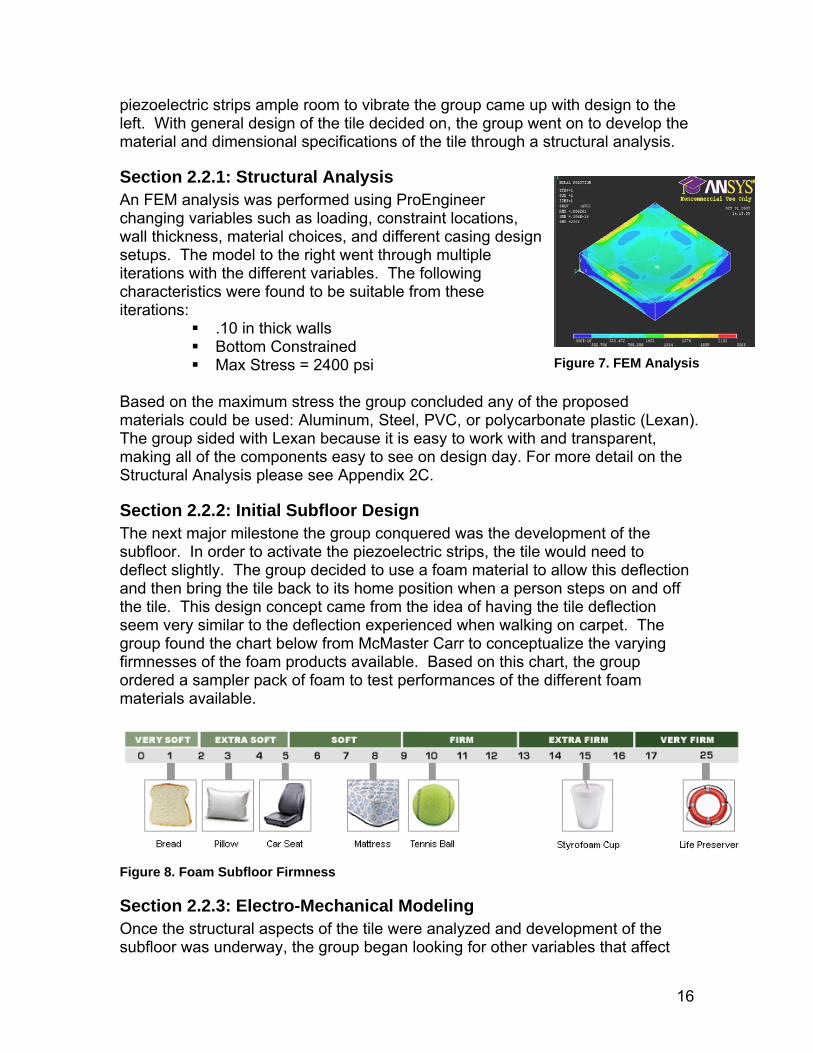
Section 2.2.1: Structural Analysis An FEM analysis was performed using ProEngineer changing variables such as loading, constraint locations, wall thickness, material choices, and different casing dsetups. The model to the right went through multipleiterations with the different variables. The followingcharacteristics were found to be suitable from these iterations:
esign
.10 in thick walls Bottom Constrained Max Stress = 2400 psi
Figure 7. FEM Analysis
Based on the maximum stress the group concluded any of the proposed materials could be used: Aluminum, Steel, PVC, or polycarbonate plastic (Lexan). The group sided with Lexan because it is easy to work with and transparent, making all of the components easy to see on design day. For more detail on the Structural Analysis please see Appendix 2C.
Section 2.2.2: Initial Subfloor Design The next major milestone the group conquered was the development of the subfloor. In order to activate the piezoelectric strips, the tile would need to deflect slightly. The group decided to use a foam material to allow this deflection and then bring the tile back to its home position when a person steps on and off the tile. This design concept came from the idea of having the tile deflection seem very similar to the deflection experienced when walking on carpet. The group found the chart below from McMaster Carr to conceptualize the varying firmnesses of the foam products available. Based on this chart, the group ordered a sampler pack of foam to test performances of the different foam materials available.
Figure 8. Foam Subfloor Firmness
Section 2.2.3: Electro-Mechanical Modeling Once the structural aspects of the tile were analyzed and development of the subfloor was underway, the group began looking for other variables that affect
16

the performance of the floor tile. It was realized early on that piezoelectric material is extremely sensitive, and that the electrical performance characteristics are dependent on the frequency of the vibrations. The group performed extensive mechanical and electrical modeling which can be found in Appendix 2A: Electro-Mechanical Modeling.
Section 2.2.4: Systems Perspective of Initial Concept The graphic below displays the breakdown of our complete system into sub-systems. For our application there are four distinct sub-systems. Each of these sub-systems was analyzed as an individual unit with their own design specifications. For each of the systems the group developed analytical models to determine specifications, which were then used as guidelines for developing the finalized model. As you can see on the graphic the four systems are the floor tile, the sub-floor, the piezoelectric composite strips, and lastly the circuitry and wireless transmission. The electrical system will be described in detail in Section 4 of this report. All of these sub-systems combine to make our modular, self powered, floor tile that transmits wireless signals upon impact.
17
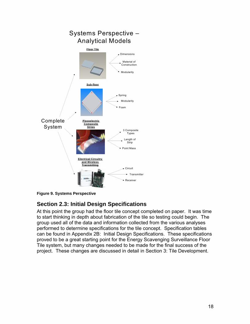
Complete System
Floor Tile
Sub-floor
Piezoelectric Composite
Strips
Electrical Circuitry and Wireless Transmitting
Circuit
Transmitter
Receiver
3 Composite Types
Length of Strip
Point Mass
Spring
Foam
Dimensions
Material of Construction
Modularity
Modularity
Systems Perspective – Analytical Models
Figure 9. Systems Perspective
Section 2.3: Initial Design Specifications At this point the group had the floor tile concept completed on paper. It was time to start thinking in depth about fabrication of the tile so testing could begin. The group used all of the data and information collected from the various analyses performed to determine specifications for the tile concept. Specification tables can be found in Appendix 2B: Initial Design Specifications. These specifications proved to be a great starting point for the Energy Scavenging Surveillance Floor Tile system, but many changes needed to be made for the final success of the project. These changes are discussed in detail in Section 3: Tile Development.
18

Section 3: Tile Development As the project proceeded, the tile went through various changes and improvements. This section discusses many of the obstacles and advancements the group faced as the project developed. The key points that will be outlined in this section are the evolution of the tile design, the obstacles faced, the newly designed strip actuation system and the prototype building phase.
Section 3.1: Design Evolution The design of the tile went through several stages as our understanding of how the tile would work developed. There were many variables to the design which were not incorporated at the initial level of our development. Below, you can see the various stages that the design went through with the key changes made at each step in the project.
The initial design incorporated the key components that needed to be included in the tile. The consisted of the four piezoelectric strips attached to a circuitry system. The shelled exterior of the tile was also developed in this stage. The design in this phase included the strips being clamped between the tile halves to limit the number of parts.
Figure 10. Initial Tile Design
The next stage in our design incorporated several changes that can also be seen in the final design. The major addition in this stage was having a new way to clamp the strips within the tile. Rather than having them between the tile halves, there would be a mounting block placed in the tile that could be used to clamp the strips independently of the tile. The other aspect that was added in this stage was using L-brackets to construct the walls of the tile. This was done to add more stability to the
exterior of the tile and eliminate the need for an adhesive which was the original idea for tile construction.
Figure 11. Second Stage Tile Design
19
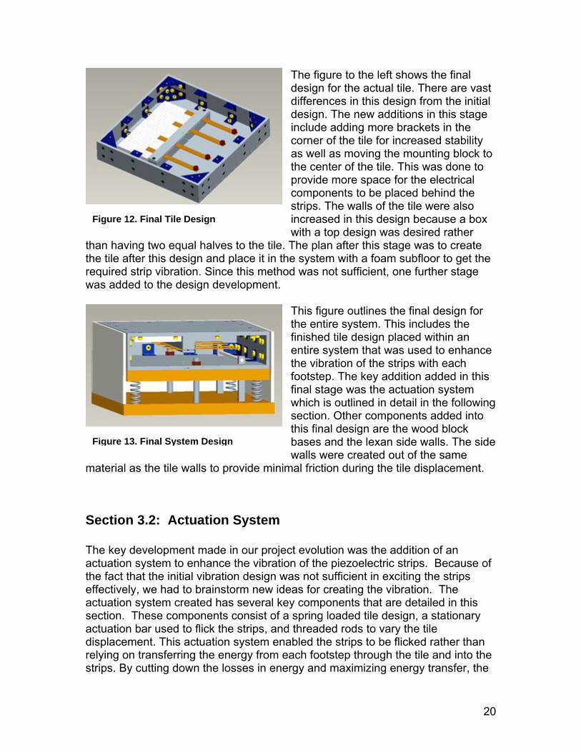
The figure to the left shows the final design for the actual tile. There are vast differences in this design from the initial design. The new additions in this stage include adding more brackets in the corner of the tile for increased stability as well as moving the mounting block to the center of the tile. This was done to provide more space for the electrical components to be placed behind the strips. The walls of the tile were also increased in this design because a box with a top design was desired rather
than having two equal halves to the tile. The plan after this stage was to create the tile after this design and place it in the system with a foam subfloor to get the required strip vibration. Since this method was not sufficient, one further stage was added to the design development.
Figure 12. Final Tile Design
ollowing
de
ement.
Section 3.2: Actuation System
he key development made in our project evolution was the addition of an se of
his
her than
This figure outlines the final design for the entire system. This includes the finished tile design placed within an entire system that was used to enhance the vibration of the strips with each footstep. The key addition added in this final stage was the actuation system which is outlined in detail in the fsection. Other components added intothis final design are the wood block bases and the lexan side walls. The siwalls were created out of the same
material as the tile walls to provide minimal friction during the tile displac
Figure 13. Final System Design
Tactuation system to enhance the vibration of the piezoelectric strips. Becauthe fact that the initial vibration design was not sufficient in exciting the strips effectively, we had to brainstorm new ideas for creating the vibration. The actuation system created has several key components that are detailed in tsection. These components consist of a spring loaded tile design, a stationary actuation bar used to flick the strips, and threaded rods to vary the tile displacement. This actuation system enabled the strips to be flicked ratrelying on transferring the energy from each footstep through the tile and into thestrips. By cutting down the losses in energy and maximizing energy transfer, the
20

group was able to achieve a much better strip vibration that could generate a functional amount of power.
Springs (4X)
Actuation Bar Assembly(Stationary)
PZT StripsAluminum Mounting
Block
Threaded Rod (4X)- controls height/spring
pre-load
LexanSidewalls
(reduce friction)
Energy Harvesting
Circuit
¾” Wood Board (2X)Allowable
Displacement (0<do<1.5”)
do
Figure 14. Actuation System
he actuation system with each of its major components can be seen in the
r
Tfigure above. For a full scale picture see Appendix 3C. As stated above, by creating this system, we were able to sufficiently actuate each of the strips fomaximum power output. A description of how the system works, along with an outline of several of its subassemblies can be seen below.
Figure 15. How the System Works
21

22
Section 3.2.1: Subassemblies
The first component that can be seen in this figure is the stationary actuation bar. The posts of this bar were designed to go through the tile and the spring system to the bottom of the system. This would enable this component to be completely stationary while the tile moved vertically past it. By keeping the bar stationary, it would allow for a significant flick in the strips as they passed the bar and were deflected. The end of the bar that the strips contact was changed a few times to
before the strip was released in passing. The
returned once it passed the actuation bar. The design of this part of the system enabled a small vibration of the strips on the
wt
he
e
f
a
ric ck
Figure 16. Stationary Actuation Bar
optimize the deflection receivedfinal design of the bar had a smooth, rounded edge on top and a sharper edge on the bottom to make sure the strip
way down followed by a full vibration That was done to increase the amoun
hen the tile returned to its initial position. of power generated from each footstep.
This component of the actuation systemis the spring load assembly. This is tportion that is responsible for the displacement of the tile with each footstep. The key components that canbe seen in the figure are the wood basboards which contain slots for the 4 springs to be housed. The selection othe springs was made based on the minimal force that would be exerted insingle footstep. More details of this
selection and sizing can be found in the section on spring choice. The design of this component allows for a maximum 1.5” displacement in the tile which can be adjusted to limit the movement from a single footstep while still sufficiently actuating the strips.
Figure 17. Spring Loaded System
This final subassembly is crucial to the performance of our strips. As you can see, it includes the four piezoelectstrips placed onto an aluminum bloand clamped down by having a small aluminum strip screwed into the bottom block. The block design provides several advantages over other options that the group had for strip mounting.
Figure 18. Strip Mounting Block

First, it enables us to place the strips anywhere in the tile, rather than constricus to just along the sides. Also, the back ends of the piezoelectric strips where the wires come out of are able to extend from the back of the mounting block. This provides us with ample space in front for the strip vibration and in the bfor the housing of ele
ting
ack ctrical components.
in e nlse ns in ent springs to use. To be safe, we used a enly distributed throughout the springs.
This would translate to a 25 pound force this amount of force displace the tile the necessary 1.5” for full displacement. We
s can
o
estrian would not notice the movement of the tile. The ilar to that of a carpet and
cement. However, several roblems were run into with this method. Once the tile was completed, we tested
Section 3.2.2: Spring Selection The selection of the springs to be used performance of our tile. We needed to fiweight of our tile at its free length, but aeven a small applied force. This was dudisplace with the footstep of any humanfront of us, we looked into several differweight of about a 100 pound person, ev
the actuation system was crucial in thd a spring that could support the full o compress a sufficient amount with to the fact that the tile would need to being. With the design consideratio
on each spring. Our goal was to have
also wanted the free length of the spring to be the 3 inches needed to have thetile flush with the top surface. The final spring selection with its specificationbe seen in Appendix 3A.
Section 3.3: Obstacles and Changes Made As is the case with any project, our tile system ran into many obstacles along our path. At several points in the design and building of our system we realized that our initial plans for the tile would not work in effectively achieving the output power we needed. Throughout the course of the project, changes were made thelp improve the effectiveness of our system. This section will detail many of the areas which required further development as our project progressed through its timeline.
Section 3.3.1: Subfloor Development The initial idea for our tile displacement was to place a subfloor under the constructed tile, made of a foam pad. This would allow the displacement to be small enough that the pedreasoning behind this design was to make the floor simreceive vibration in the strips from that small tile displapits abilities using several different subfloors. From this testing, we discovered that the tile we had created was too rigid and that the energy from each footstep was not being translated into the piezoelectric strips. The power outputs achievedfrom these tests were minimal, and an alternate idea was decided upon. This was the major cause for the newly designed actuation system that was detailed in the previous section.
23

Section 3.3.2: Using Magnets as Point Masses
ts were able to increase the vibration amplitude while keeping the frequency well within the range of maximum power output.
ection 3.3.3: Uneven Displacement of the Tile
r.
m e
nt
testing and for displaying omponents on design day. It is easily assembled and disassembled as well as
d
ponents and materials used the
mounting of the piezoelectric strips could easily be integrated into the molding of sideration would be to have the two
As a way to enhance vibration in our strips, the group decided to put point masses at the end of each of the strips. Initially, the idea was to find a dense mass that would be small in size but high in weight to increase the amplitude of the strip vibration as much as possible. However, the group soon realized that by doing this, we were significantly reducing the frequency of vibration which is key in acquiring optimal power output. After this conclusion, the group decided that the actuation of the strips was sufficient without and point mass on the strips. After testing several times without any mass, the group decided we still needed to optimize the vibration slightly. The final design includes two magnets placedtowards the end of the strips. These are placed on each side of the strip and attached using heat shrink tubing. Through testing, the group was able to conclude that the magne
S With the initial design of the actuation system, we were sometimes receiving uneven displacement from each footstep. Unless the tile was stepped on directlyin its center, certain sides of the tile would depress more than others. The main cause for this was because there was a 1/8” gap included on each side of the tileto eliminate any possibility of galling from the plastics rubbing against each otheThe solution decided upon was to place a gap closer on each side of the systeto ensure the tile would move only directly up and down. There was also a smallamount of grease placed between the two plastics to ensure smooth travel. Oncthis change was made, the force on the tile would cause an equal displacemeregardless of which part was stepped on.
Section 3.4: Prototype Building The design of the prototype tile is ideal for optimization cbeing transparent. However, a production version would definitely be designeand constructed differently. The inner workings of the system would remain very similar although optimized even further to reduce unit cost. The main differenceswould be in the material and construction method used in producing the tile structure. The group chose Lexan for the prototype for its transparency and suitable strength, but a production model would most likely be made of high strength injection-molded plastic or stamped out of metal. The tile could be molded in two separate halves that could be assembled using press-fit fittings. This would prove to be material efficient as well as much labor intensive than theprototype. To decrease the number of com
the bottom half of the tile. One other con
24

25
e
tile
p had a large amount of work to do in a small mount of time. While the tile was fully constructed, the exterior box and the
ed, king
halves easily separable. This would support maintenance and repair of the floor tiles in the field when necessary. When building the prototype, the group discovered several other areas that could make future building of such a tile much easier. The major area for improvement would be to reduce the number of screw holes necessary for thtile construction. In our current design, we included numerous L-brackets to ensure proper support for the tile. However, with each of these supports, the required countersunk holes and screwing processes which take up sufficienttime during manufacturing. To reduce this, the group would limit the number of L-brackets necessary to still make the tile completely stable. For our design day prototype, the group wanted to make a fully usable system incorporating our tile design as well as our actuation system. Because of the fact that the actuation system was not incorporated until only a few weeks before senior design day, the grouaspring loaded system would need to be developed. As the prototype developwe were able to make changes as we saw them necessary to make a worprototype for our final testing. A picture of the final prototype in use can be seenin the figure below.
Figure 19. Final Prototype

Section 4: Electrical System
Figure 20. Electrical Systems Diagram
Figure 21. Placement of Electrical Systems in Tile
*See Appendix 4A for a Full Circuit Diagram, Appendix 4B for data sheets and electrical parts list
Energy Harvesting Circuit
Input from Piezo Strips
Output
Rectifiers
26

Section 4.1: How the Electrical System Works This section will provide detailed design and functionality specifications of the main electrical components of this project. Shown above in Figure 20 is an Electrical Systems Diagram illustrating the overall concept. The major components include:
1) Four piezoelectric strips mounted in the floor tile – output AC voltage 2) Full wave bridge rectifiers – to rectify each AC output to DC 3) ALD EH301 Energy Harvesting Circuit – to store energy 4) PIC16F877a Microprocessor – powered by energy harvesting circuit,
programmed to wake up Zigbee Transmitter 5) Zigbee Transmitter – to send signals 6) Zigbee Receiver – to receive signals 7) PC Terminal with Graphical User Interface (GUI) to provide a “WARNING”
alert The first component is the oscillating piezoelectric strips mounted inside the spring actuated floor tile. To increase output voltage 4 piezoelectric strips were incorporated into the final prototype. The strips output AC voltage, which is not
here exists the potential for the strips to be tructive interference of the AC waves
if connected together, with the potential for major losses in power. Therefore, the output from each strip was passed through individual rectifiers on a protoboard mounted in the tile and connected in parallel to the energy harvesting PCB. Due to using the energy harvesting PCB, impedance matching was no longer a concern. According to our sponsor Advanced Cerametrics, the energy harvesting PCB addresses the impedance matching issue. The second major component is the energy harvesting circuitry. The group used an energy harvesting PCB (EH301) developed by Advanced Linear Devices (ALD). A data sheet is provided in Appendix 4B for additional information about
commercially available product was discovered after mpts of creating a homemade circuit. The low power output and
variability of the input voltage spikes make it very difficult to store and retain power. Previous attempts were nullified by power losses in circuit components and fast capacitive discharge rates that exceeded input power, renegligible net captured energy. The EH301 Energy Harvesting Circuit solves these issues. It is able to take electrical charge packets that arrive in a wide range of voltages, currents and timing waveforms and is able to accommodate such conditions with exceptional efficiency and effectiveness. The circuit is able to store these small energy packets in a 1000uF capacitor, retain this energy and condition the voltage using
operates in the 3.1 to 5.2 V to
characteristics:
easy to combine the four outputs. Tvibrating out of phase, which can cause des
the product. Thisunsuccessful atte
several
sulting in
regulators to power useful output. The EH301power the PIC16F877a Microprocessor chosen. The circuit has the following
27

1) Energy Efficiency – circuit is roughly 90% efficient in order to maximize net
on - to store the captured energy for as long as possible
ut rocessor)
captured energy Net captured energy = energy available – energy EH circuit consumes
2) Energy Retenti
with minimal leakage or loss the outp3) Energy Management - condition the stored energy to provide
ropnecessary for the desired application (in this case the mic4) Useful Energy Output of 8.3mJ (1000uF capacitor b/t 3.1 and 5.2V)
Figure 22. Energy Harvesting Circuit Schematic
The third component is the microprocessor. The group used a PIC16F877a microcontroller obtained from the Stevens Engineering Design 1 Lab, which haan operating voltage between 3.3 and 5 Volts. The microprocessor is powered from the output discharge of the capacitor in the energy harvesting circuitry. Power and a USART signal are then provided to the ZigBee transmitter. This program runs in a loop until the capacitor is drained beyond the necessary lto power the microprocessor. Fo
s
evel r more information on the microprocessor, see
e attached data sheet in Appendix 4B.
ves a
is
th The fourth and final electrical component is the ZigBee transmitter. The transmitter is powered to 3.3 volts from the microprocessor, which receives its power from the Energy Harvesting Circuit. At that time, the transmitter receiUSART signal from the microprocessor and it transmits a warning signal to a receiver terminal. The power supplied from the microprocessor is 5 volts. Thisreduced to 3.3 volts using a voltage divider where R1 = 3K and R2 = 5K.
28

Section 4.2: Testing of Electrical System The most critical test was verifying the performance of the energy harvesting circuitry. The test setup rene gy
d he e
ea unt of flicks is recorded again. This test was most significant, because it enabled us to determine the output energy available to power the microprocessor. The microprocessor was tested to verify the USART signal was being sent properly. To do this, the microprocessor was powered with a power supply, and the programmed output pin was connected to an oscilloscope. The oscilloscope was then adjusted to adequately view the signal. This test was crucial to determine of the proper USART signal was being sent to the ZigBee Transmitter. Also, to determine of the pins were set correctly, a resistor was placed in series with an LED running to ground. This was a simple test to verify the outputs. The test for the ZigBee transmitter was the least complex. The ZigBee was powered with a power supply to 3.3 volts. The microprocessor sends the USART signal, and the output at the receiver terminal was watched. If a packet is received, the transmission was successful.
Section 4.3: Performance of Electrical/Wireless System
ry too much from the planned
. mV t
equired one piezoelectric strip, a bridge rectifier, and the harvesting device from ALD. The positive and negative outputs of ther
strip were connected to the positive and negative input of the bridge rectifier, anthen the energy harvesting PCB. A multimeter was connected to the output of tcapacitor on the PCB (positive lead) and ground of the PCB (negative lead). Thstrip was then flicked until the capacitor reached 5.2 volts and discharges to 3.1
he level of voltage increase was noted as the capacitor charges after volts. Tc flick. After the discharge, the process was then repeated and the amoh
The capabilities of the final design did not vaoutcomes. The final prototype was able to charge a 5.3 volt capacitor from 3.1 volts to 5.2 volts in approximately 20 steps on the tile, as will be elaborated uponmore fully in Section 5 of this report. To test this, the energy harvester’s V+ pin, which measures the voltage on the capacitor, was measured using a multimeterWhile stepping on the tile, we were able to observe an average charge of 100per step. The microprocessor was programmed to turn on an LED, and when iturns on, it would denote exactly when the harvester reached 5.2 volts. Figure 23 shows the breadboard circuit and the LED connected to the microprocessor.
29
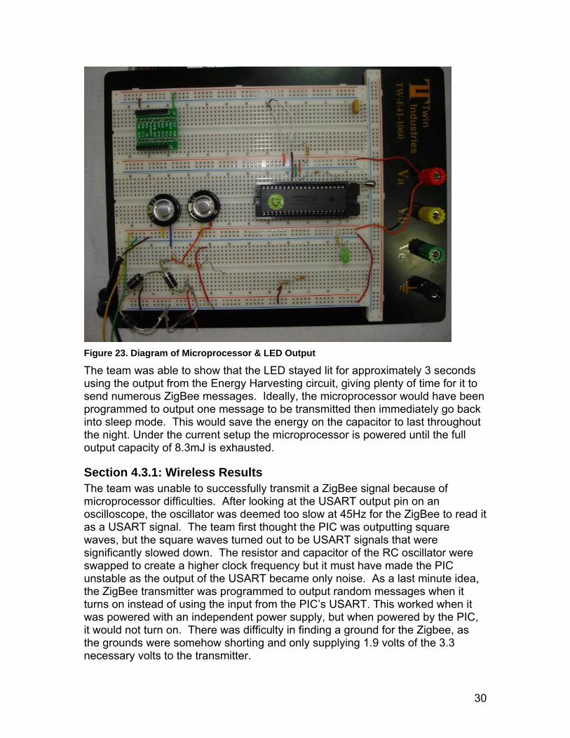
Figure 23. Diagram of Microprocessor & LED Output
The team was able to show that the LED stayed lit for approximately 3 seconds using the output from the Energy Harvesting circuit, giving plenty of time for it to send numerous ZigBee messages. Ideally, the microprocessor would have been programmed to output one message to be transmitted then immediatelyinto sleep mode. This would save the energy on the capacitor to last th
go back roughout
ull
swapped to create a higher clock frequency but it must have made the PIC unstable as the output of the USART became only noise. As a last minute idea, the ZigBee transmitter was programmed to output random messages when it turns on instead of using the input from the PIC’s USART. This worked when it was powered with an independent power supply, but when powered by the PIC, it would not turn on. There was difficulty in finding a ground for the Zigbee, as the grounds were somehow shorting and only supplying 1.9 volts of the 3.3 necessary volts to the transmitter.
the night. Under the current setup the microprocessor is powered until the foutput capacity of 8.3mJ is exhausted.
Section 4.3.1: Wireless Results The team was unable to successfully transmit a ZigBee signal because of microprocessor difficulties. After looking at the USART output pin on an oscilloscope, the oscillator was deemed too slow at 45Hz for the ZigBee to read it as a USART signal. The team first thought the PIC was outputting square waves, but the square waves turned out to be USART signals that were significantly slowed down. The resistor and capacitor of the RC oscillator were
30

In testing the Zigbee, a GUI was designed so when the receiver received any packets of data from the transmitter, it would change to a red screen with “WARNING” written across it (Figure 24).
Figure 24. Terminal GUI
This was used as an easy way to distinguish if the receiver was receiving data. The transmitter was supplied 3.3V from a power supply and had the USART output of the PIC to the Din pin. Using this configuration, we would troubleshoot the USART signal to try to understand why it would not work correctly. An LED
tatus of the transmitter as on or
ful ran through its programmed logic by r approximately 3 seconds. The Zigbee
al
was also connected to the ON pin to show the soff, and another LED connected to the transmitter that would be lit when the transmitter was communicating with the receiver. The receiver was connected toa laptop via the supplied Maxstream board.
Section 4.4: Electrical Performance Summary In all, the group was able to harvest energy in a new and unique application. TheEnergy Harvesting Circuit was connected to the microprocessor, and it was shown that the microprocessor successlighting up an LED on its output pin foworked independently of the microprocessor using a power supply, but wasunable to be successfully implemented into the design. Since the electrical system development was performed concurrently on a different project team, the integration of the two systems was slightly incomplete. The only missing link was the powering of the Zigbee transmitter by the microprocessor. With additiontime, this problem could be eradicated.
Figure 25. Missing Design Objective
The only design objective that was incomplete was the link between the microprocessor and Zigbee transmitter.
31
Section 5: Testing and Results
Setup Actuation System
Measure # of Judge relative feasibility of the test condition
footstrikes to charge circuit
Test Variables• # of PZT strips
• # of magnets
• Location of triggering mechanism
• Spring pre-load
• Weight of test subject
Multimeter
Choose Final Configuration
voltage data allows for the
ilable – energy
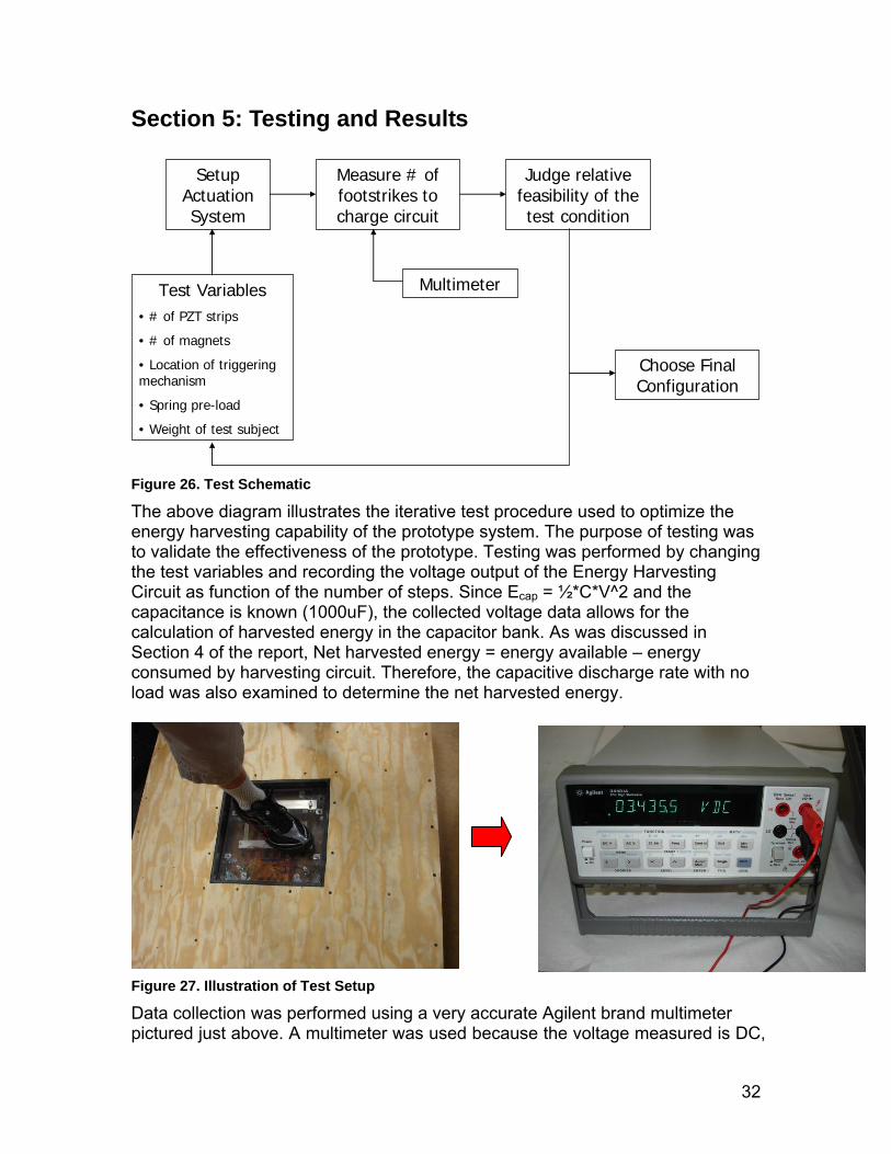
Figure 26. Test Schematic The above diagram illustrates the iterative test procedure used to optimize the energy harvesting capability of the prototype system. The purpose of testing wasto validate the effectiveness of the prototype. Testing was performed by changingthe test variables and recording the voltage output of the Energy Harvesting Circuit as function of the number of steps. Since Ecap = ½*C*V^2 and the capacitance is known (1000uF), the collectedcalculation of harvested energy in the capacitor bank. As was discussed in Section 4 of the report, Net harvested energy = energy avaconsumed by harvesting circuit. Therefore, the capacitive discharge rate with no load was also examined to determine the net harvested energy.
Figure 27. Illustration of Test Setup Data collection was performed using a very accurate Agilent brand multimeter
was used because the voltage measured is DC, pictured just above. A multimeter
32
measured across the leads of the 1000uF caarvesting Circuit.
pacitor in the EH301 Energy
Section 5.1: Test Results *For actual test result data see Appendix 5A. The following test conditions were run:
• No point mass, 1 piezo strip • No point mass, 4 piezo strips • 1 magnet, 1 piezo strips • 1 magnet, 4 piezo strips • 2 magnets, 1 piezo strip • 2 magnets, 4 piezo strips
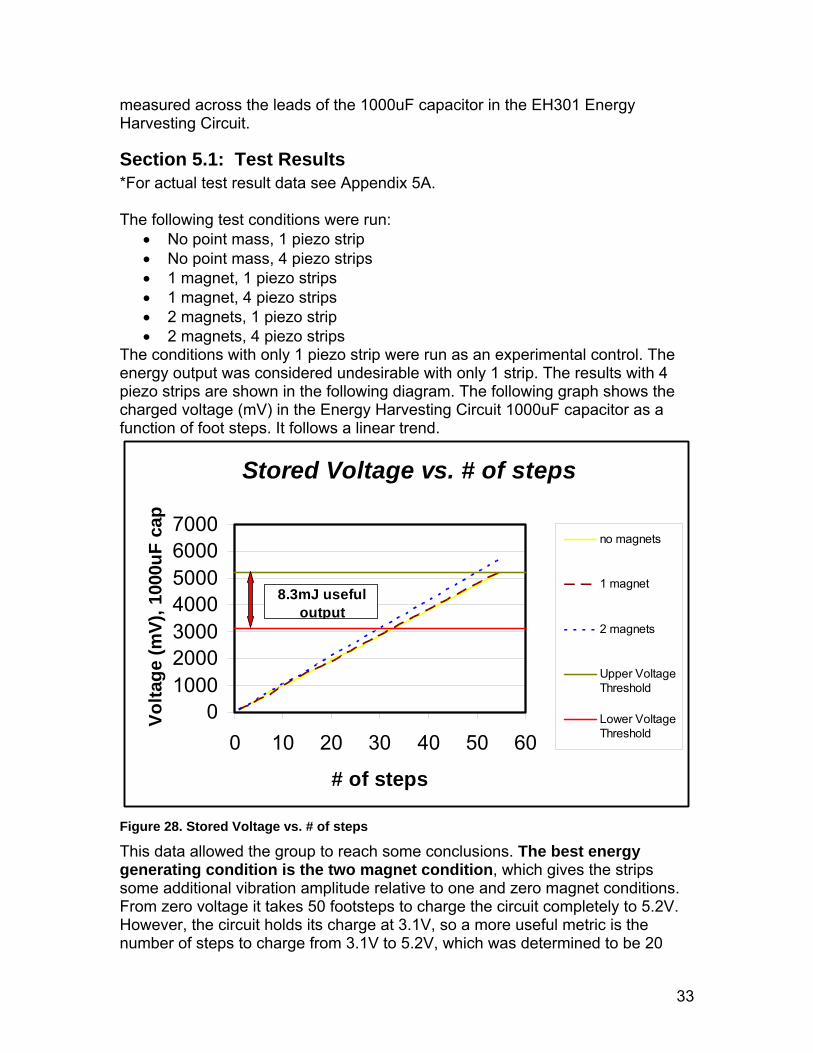
The conditions with only 1 piezo strip were run as an experimental control. The energy output was considered undesirable with only 1 strip. The results with 4 piezo strips are shown in the following diagram. The following graph shows the charged voltage (mV) in the Energy Harvesting Circuit 1000uF capacitor as a function of foot steps. It follows a linear trend.
H
Stored Voltage vs. # of steps
30004000500060007000
mV)
, 100
0uF
cap
010002000
0 10 20 30 40 50 60
# of steps
Volta
ge (
no magnets
1 magnet
2 magnets
Upper VoltageThreshold
Lower VoltageThreshold
8.3mJ useful output
Figure 28. Stored Voltage vs. # of steps
This data allowed the group to reach some conclusions. The best energy generating condition is the two magnet condition, which gives the strips
tive to one and zero magnet conditions. tsteps to charge the circuit completely to 5.2V.
some additional vibration amplitude relaFrom zero voltage it takes 50 fooHowever, the circuit holds its charge at 3.1V, so a more useful metric is the number of steps to charge from 3.1V to 5.2V, which was determined to be 20
33
footsteps. Therefore, this data supports that 8.3mJ of useful output cagenerated in just 2
n be 0 footsteps on the floor tile!
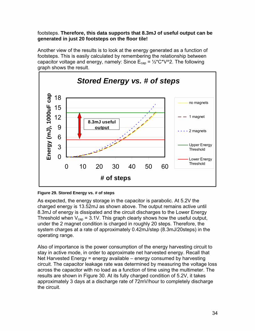
ok at the energy generated as a function of
ering the relationship between apacitor voltage and energy, namely: Since Ecap = ½*C*V^2. The following
Another view of the results is to lofootsteps. This is easily calculated by remembcgraph shows the result.
Stored Energy vs. # of steps
03
0 10 20 30 40 50 60
# of steps
Ener
gy (
18cap
no magnets
69
12
mJ)
, 100
0u
15F
1 magnet
2 magnets
Upper EnergyThreshold
Lower EnergyThreshold
8.3mJ useful output
Figure 29. Stored Energy vs. # of steps
As expected, the energy storage in the capacitor is parabolic. At 5.2V the charged energy is 13.52mJ as shown above. The output remains active until 8.3mJ of energy is dissipated and the circuit discharges to the Lower Energy Threshold when Vcap = 3.1V. This graph clearly shows how the useful output, under the 2 magnet condition is charged in roughly 20 steps. Therefore, the system charges at a rate of approximately 0.42mJ/step (8.3mJ/20steps) in the operating range. Also of importance is the power consumption of the energy harvesting circuit to stay in active mode, in order to approximate net harvested energy. Recall that
ilable – energy consumed by harvesting
he
Net Harvested Energy = energy avacircuit. The capacitor leakage rate was determined by measuring the voltage loss across the capacitor with no load as a function of time using the multimeter. Tresults are shown in Figure 30. At its fully charged condition of 5.2V, it takes approximately 3 days at a discharge rate of 72mV/hour to completely discharge the circuit.
34

Since the discharge rate is known, the equilibrium rate of steps/hour can be determined that matches input energy to lost energy. It was shown that energy is
arvested at 0.42mJ/step in the operating range, which is approximately ng
tem wn with no load. This result shows that the energy loss
has a negligible effect on net energy transfer and that the circuit energy retention rate is extremely good.
hequivalent to 100mV/step charged in the 1000uF capacitor. Solving the followiequation: [100mV/step * X steps/hour = 72 mV/hour] yields a result of 0.72 steps/hour. So as long as the tile is stepped on at least once per hour the syswill not discharge on its o
Capacitor Leakage Rate (no load)
01000
20003000
40005000
6000
0 1 2 3
Upper VoltageThreshold
Days
Volta
ge (m
V) Leakage/dayEnergy Harvesting Circuit holds charge for 3 days!
Leakage Rate =72mV/hour
Figure 30. Capacitor Leakage Rate of Energy Harvesting Circuit
Section 5.2: Summary of Test Results The following table summarizes the test results of the system with four piezoelectric strips with 2 magnets mounted on each strip. Steps to charge circuit from 0-5.2V 50 Steps to charge circuit in operating range (3.1-5.2V) for 8.3mJ useful power
20
Stored Energy/step in 3.1-5.2V range 0.42mJ/step Capacitive Discharge with no load 72mV/hr (in 1000uF capacitor) Footstep rate for zero net energy transfer 0.72 footstep/hr Table 1. Summary of Test Results
35

Section 5.3: Wireless Transmission Capability Although the full wireless functionality of the system was not fully recognized (as explained in Section 4.3), the power requirements for several wireless signals were successfully generated by the system. Useful Energy Output 8.3mJ Energy Required/Wireless Transmission 1.44mJ Wireless Transmission Capability 5.76 signals Table 2. System Wireless Transmission Capability
The above table shows that given the 8.3mJ output capability of the EH301 Energy Harvesting Circuit, 5 wireless signals can be sent with a 1.44mJ per signal power requirement. Therefore, 20 footsteps generate enough power to send 5 wireless signals.
36

Section 6: Project Conclusions This section of the report will act as a culmination of all the lessons learned while ompleting this Senior Design process. Also included in this section will be any
mendations of the group's specific application for this al proto ld act as a great
sign groups desiring a similar application.
ment for
was able to prove that they could harvest power
ould be enough to power both a logic controller and a wireless transmitter that
could be used for surveillance purposes. After completing the designed prototype the group had an opportunity to look at the project as a whole and compile a punch list of changes that could have been made if the timeline allowed for it. These suggestions would be a great starting point for future design teams if they chose to pursue a similar application using the same technology. In order to get a full understanding of the need for change within the prototype the group thought it was fit to populate a list of downfalls that the prototype had, along with possible solutions for each issue. The results of this assessment can be seen below.
Problem or Flaw Suggested Solution or Improvement
cimprovements or recomtechnology. This proof of design conceptu type woustepping stone for future senior de
Section 6.1: Suggestions for ImproveAs a whole the group felt that they achieved the objectives that they set forththemselves at the beginning of this design process. Using the piezo strips
eveloped by ACI the groupdfrom the mechanical forces created when taking a step across an average floor ile. In addition, the group was able to prove that the amount of energy harvestedtw
A displacement of 1.5 inches would be noticeable while casually walking
across a network of floor tiles.
A complicated mechanical mechanism could be used to translate a much
smaller vertical displacement into a large displacement of the PZT
composite strips.
One tile would be avoidable by any intruder.
The tile should be installed in a network that would allow for each tile to be dropped into place and become
instantly fully functional.
37
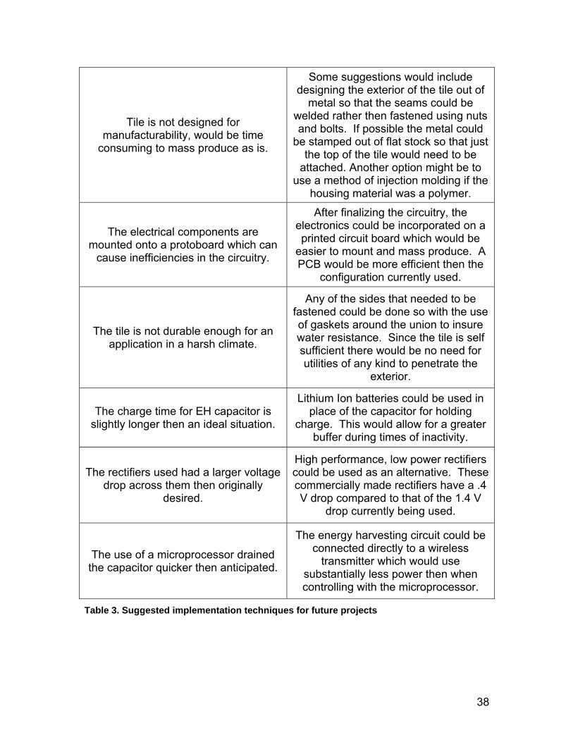
Some suggestions would incdes
Tile is not designed for manufacturability, would be time
consuming to mass produce as is.
welded rather then fastened using nuts and bolts. If possible the metal could
be stamped out of flat stock so that the top of the tile would need to
attached. Another option might be t
lude igning the exterior of the tile out of
metal so that the seams could be
just be
o use a method of injection molding if the
aterial was a polymer. housing m
The electrical components are mounted onto a protoboard which can
cause inefficiencies in the circuitry.
After finalizing the circuitry, the electronics could be incorporatedprinted circuit board which would b
easier to mount and mass produce. APCB would be more efficient then the
configuration currently used.
on a e
The tile is not durable enough for an application in a harsh climate.
fastened could be done so with the useof gaskets around the union to insure water resistance. Since the tile is self sufficient there would be no need forutilities of any kind to penetrate the
Any of the sides that needed to be
exterior.
The charge time for EH capacitor is slightly longer then an ideal situation.
Lithium Ion batteries could be used inplace of the capacitor for holding
charge. This would allow for a greater
buffer during times of inactivity.
The rectifiers used had a larger voltage could be us
V drop across them then originally
desired.
High performance, low power rectifiers ed as an alternative. These
commercially made rectifiers have a .4 drop compared to that of the 1.4 V
drop currently being used.
The use of a microprocessor drained the capacitor quicker then anticipated.
The energ could be
substantially less power then when co .
y harvesting circuitconnected directly to a wireless
transmitter which would use
ntrolling with the microprocessor
Table 3. Suggested implementation techniques for future projects
38

Section 6.2: Alternate Uses and A When taking a step back and looking at thup with a few applications using similar coactivities with repetitive foot striking. Somwe
• Light up gaming application using tof the user to power LEDs embeddfabric of the dance pad.
• Location monitoring of: equip
conlight timing based on traffic flow.
• Dance floors in bars or clubs that wouusing the power of the people's mo
• An application within the sole of a say
Section 6.3: Recommendations As stated previously the group felt that this project would be a great stepping sto appthis in mind the group thought that some ot pthe group would pass on are:
a
nitude• When using these ACI developed PZT
understand the relationship between both frequency and ampliturespect to the voltage generated.
atchi y need be ibra
• In the case of using a discontinuous forced vibration, an actuation system is essential to get optimal performance. Discontinuous, translated
d transmission of mechanical to electrical energy without the use of such an actuation system.
pplications
e project as a whole the group came ncepts. This included numerous e of the ideas that group thought of
he footsteps ed into the
re:
o Cars or other industrialo Pedestrian traffic o Animals
• Traffic light sensors to aid in the
ment
trol of traffic
ld light up vements throughout the room. hoe that might help to power small walking. personal electronics from everyd
ne for a future group working on an
wo semesters would be helpful in this ty
lication using the same material. With f the lessons learned during the last e of situation. Some suggestions that
• Due to the nature of this material, along with it, it is highly suggestedtaking on a project of this mag
nd the unknown specifications that go to have ample electrical support when
. composites it is important to
de with
• The group found that frequency mdiscontinuous vibration. The onlif there was a continuous forced v
ng was not needed in the case offor frequency matching would
tion.
Figure 31. Sample Dance Pad
vibrations within a structure will not correspond to goo
39

Section 6.4: Conclusion he group began this project with the following two objectives in mind: T
• Utilize the unique properties of PZT (lead zirconate titanate) fiber-
based piezoelectric materials developed by Advanced Cerametrics Company to design and develop a floor tile that harvests energy from a foot strike.
of power to transmit
ish the goals that they set forth for themselves at constructed during the spring
se mechanical forces created while walk seful electrical energy. Using energy
able to demonstrate that ac
f-ss to be very fulfilling and
ry steps to designing and testing a ce and believed that it would help them
roughout all of their future endeavors in the engineering field.
• Use the harvested energy as the sole sourcewireless signals for building surveillance.
lThe group was able to accomp
the start o if th s design process. A prototype was use the wasted mester whose purpose was to
into a uing and convert themharvesting circuitry and a logic controller the group was the 8.3 mJ of useful power harvested in the 1000 μF cap itor would be enough to send out five wireless signals during off hours. The final prototype proved to be a self-sufficient system that could be independently placed in the field and used for surveillance purposes during ofhours. In addition, the group found the design procehelped them to understand all the necessaprototype. The group valued the experienth
40

References Articles:
iber Technology at Advanced Cerametrics.” F.Mohammadi, H. kim, “FJerryRuddle and, R. B. Cass. 9 Oct 2007.
“C ices for Recharging atteries.” Henry A. Sodano and Daniel J. Inman. Virginia Polytechnic Institute
rain, Inc.
uency
l. 86, No. 10. Websites: Supplier of Piezoelectric Material: Advanced Cerametrics Company: www.advancedcerametrics.com
omparison of Piezoelectric Energy Harvesting Dev
Band State University. “Modules Will Harvest Energy For Remote-Sensor Networks.” David Morrison. Ed. Power Electronics Technology. “Strain Energy Harvesting for Wireless Sensor Networks.” D.L. Churchill, M.J. Hamel,C.P. Townsend, S.W. Arms.© 2003 MicroSt “A vibration energy harvesting device with bi-directional resonance freqtenability. “Vinod R. Challa, M.G. Prasad, Yong Shi and Frank T. Fisher.Department of Mechanical Engineering, Stevens Institute of Technology “Advanced Cerametrics Harvests Clean Energy.” Jerry Ruddle, Richard Cass and Farhad Mohammadi. American Ceramic Society Bulletin, Vo
Supplier of Energy Harvesting Circuit: Advanced Linear Devices: www.aldinc.com Supplier of Mechanical Materials: McMaster Carr: www.mcmaster.com Supplier of Electrical Materials: Mouser: www.mouser.com DigiKey: www.digikey.com “Power from the People” http://www.wired.com/culture/lifestyle/commentary/imomus/2006/08/71582 Google Patent Search: http://www.google.com/patents Japan Industrial Property Digital Library: http://www.ipdl.inpit.go.jp
41

42
Piezoelectricity: http://en.wikipedia.org/wiki/Piezoelectricity ://en.wikipedia.org/wiki/Strain_gaugeStrain Gauge, http
m/Nd/2006106570.htmlFloor generation in Tokyo train station, http://www.narinari.co
s Griot: http://www.mgkk.comCVI Melle 9a_nr.htmlBoeing New Release, http://www.boeing.com/ids/news/2007/q2/07052
Practice Range, http://www.practicerange.com/detail.aspx?ID=654 ump USA, J http://www.jumpusa.com/golf_training.html
PJCA, http://www.free-golf-swing-tips.com/golf-slice-fix.html Evision, http://www.evisiongolf.com/support/swing.html

Appendices
Appendix 1A: Details of Initial Five Innovative Ideas
the over-eeded to stabilize ide lateral support.
f the brace joint, and send signals to a microprocessor. The amount of bend on the material, as well as the frequency of the material oscillation will allow for logic-based programming into the microprocessor.
Another subsystem will be installed to dampen/prevent motion should conditions become unsafe for the patient. This is essentially an active damping system, actively controlled by the microcontroller. This concept could also use the bending of the material as an energy harvesting device, possibly to recharge the batteries which power the microprocessor to create a self-sustaining device that will always work. If the batteries in such a system were to fail, the logic from the microprocessor would disappear, and the device’s active damping system would fail. Constantly re-charging these batteries could serve as a fail safe to ensure the system always works as it was designed. 2. Game or Toy Application
One application that our group has looked into using piezoelectric energy for is a game or toy for younger children. The use of electronics in children’s toys is very common in order to prove the aesthetics of the game and make it more exciting for the children playing them. These electronics can include flashing LED’s or sounds that come from the game. Often, such a feature would require a battery to charge the electronic system. However, in a game that includes a significant amount of motion from its players, it may be possible to run the game solely using piezoelectric energy. This is useful for several reasons. First, it will be helpful for marketing to parents because they won’t have to spend the extra money on batteries for the product. Also, it could help in the reduction of battery usage which has proven harmful to the environment. Since batteries are hard to dispose of properly, they create a significant amount of harm to the environment, making such a game environment friendly. The idea we have thought of for the game would be similar to that of the current game called Hungry, Hungry Hippos. In such a game, up to four players will be repeatedly tapping a small lever responsible for applying a motion to the piezoelectric material. The energy would then be used to power an electronic scoreboard or sounds that come out of the game board. With that as the targeted goal for the piezoelectric material, there is a variety of game ideas that can be branched from such an activity. Clearly, the best option would be to make a game that maximizes the use of the levers to obtain the most energy possible from the piezoelectric material. One way to do this is to make it so that
1. Medical Device – Auto-Stiffening Knee Brace ric material is One application within the medical device field for piezoelect
ould senseto develop an auto-stiffening knee brace. This concept wextension of the knee, and provide additional support when n
y provthe patient. As it currently stands, most knee braces onlThis application would place the piezoelectric material o
43

each time you press your lever, you have a piece that extends towards the center . The object would be to get your piece to the center of the
nclude an obstacle of some sort to inhibit the players from
hno
.
o
o f
rs
the closing doors. wev currently utilized are not sensitive enough to ect
ing
of the game boardgame board first, but ijust blindly pressing their levers as fast as possible.
refined, the idea of the While the object of the actual game could still be tec logy being used would probably stay the same. By eliminating the use of batteries, the group could create a product which is very marketable on the toy market. However, there could be some issues with such a use of the technologyAt this time, we are unsure of the exact power output we would be able to acquire from such an application and whether or not it will be enough to power the game board. Since most of the information we have tells us that the energy is in the range of milliwatts, we would need to be able to acquire it quickly and store it for usage. Also, the electronics we use for the game would not be able tbe high powered, but probably LED type lights that require small amounts of energy. If such an application is chosen, there are many areas we would need tcomplete further research on, but overall, the product would be useful because oits marketability. 3. Sensing/Monitoring Application
One application of piezoelectric material proposed here is the piezoelectricdoor sensor for transportation modes such as trains and buses. Automatic dootoday that are powered by motors or compressed air often have some kind of
etection system, in case an object is caught betweendHo er, the mechanisms that aredet small objects such as fingers, the tip of an umbrella or things that can be compressed to a thin size such as backpacks and handbags. There have been accidents when a train has started moving, while the leg of the baby stroller was stuck between doors as well as a time that a child got caught in automatic revolving door. The consequence can clearly be fatal. Piezoelectric sensing is ideal to replace the current design of detection system by placing the strip of piezoelectric fiber along the edge of the door or inside the rubber cushion. When an object is caught in between doors, the piezo sensor is bent and voltage created can be used as a signal that indicates that something is jammed. A control unit can then reduce the force to make it easier to pull the object out or can stop the movement of the closing door until the object clears. A piezoelectric sensor which can create voltage in response to small mechanical strain will be more sensitive to detect small objects and as a result, it will be much safer for people going through doors. In the following paragraphs, several other door sensors that are currently used are described for comparison with piezoelectric sensor. First, the most widely used design for detecting obstacle, is to use an infrared beam. Door unitsrecognize the object or person when the IR beam emitted vertically or horizontally is intercepted. This mechanism is often used in European trains where the train does not get very crowded. However, this cannot be used for congested trains where people are standing very close to the door or overflowbecause the IR beam will remain intercepted and the door will never be closed.
44

The area of detection is limited, depending on the number of IR sensors, and it is still possible that the person or object slips out through the detection. It is advantageous in the way that it can sense the obstacle before the door hits the person or object. second design takes advantage of the electric motor that powers the doin which the load on the motor or torque applied is increased because of an obstacle in between the doors. The motor has to deliver more torque to close thdoor if there is something that blocks the movement of the door. A control unit then reduces the torque or stops flowing electricity to make it easier for theobstacle to be pulled out. This mechanism is useful in the case of a crowded tradescribed earlier where the door has to be kept closing no matter what is getting caught, and does not need extra devices for detection. A drawback of this mechanism is that if an obstacle is too small, the door closes almost completely leaving only a tiny space and it cannot detect an object as the motor is stoppeAlso, the door continues to close slightly after detection because of inertia and there is some delay in responding. The third de
A or
e
in
d.
sign is similar to the second design, but this method utilizes a ressure sensor mounted in the rubber along the edge of door. This mechanism
change in electrical resistance in respon
dge of
e
en in goes
1 ,
he object is pulled away a few seconds after the
door.
pis the same as a strain gauge which measures
se to the deformation. This design is highly sensitive to a small load, and it is relatively cheap. However, unlike a piezoelectric sensor that is self powered and creates voltage by itself that can be used as signal, it still needs an outsidepower source to operate. Comparison of alternatives mentioned above issummarized in a matrix in Appendix 1B.
As it can be seen from the comparison matrix, piezoelectric sensor ranks the highest except for the detection before touching or catching the object. To use a piezoelectric sensor on the door, it is expected that an axial piezo sensor is placed in the rubber as a protection and placed along the ethe door, as it is done with a pressure sensor. In the case of a plug door wherethe door opens to the outside of the body, a piezo sensor can be placed on thother side as well to detect human fingers getting caught when the door is opening. The picture of the door showing the location of a robber can be sethe appendix. When the object is caught, voltage of the piezoelectric sensor up. At that moment, a control unit recognizes the object being caught. Unlike thepressure sensor with a strain gauge inside in which electric resistance is kept high as long as the object is stuck, piezoelectric material loses voltage in about second, so it may not know when the object is pulled out. To solve this problema control unit recognizes that tlast voltage ramp is measured because if something is stuck, it is natural that the person would keep moving the object or hand until it is pulled away from the This would create a voltage as long as it stays in between the doors.
45

4. Buoy Light or Ocean/Wave Application - Self Sustained
Navigation/Sensing Buoy System There is a multitude of buoys in the ocean. Most of these buoys are for
navigation or some sort of sensing application. All buoys have one thing incommon, that is, they require navigation lighting as well as some sort of system in order to power the navigation lighting on all the buoys in the ocean. Some of these systems are powered by batteries that, once dead must, be replaced. Other buoys utilize solar panel which
recharges a battery during the daylight r
y
ieve this to be possible by starting the design
ss
lf club, in order to effectively create a swing training aid. As the sport of golf continuous to flourish in recent years among all age groups, there is an ongoing market for golf accessories and training aids. This product will allow the golfer to modify their swing from a slice to a fade, and anywhere in between. This club will be able to
hours, and then at night the charged battery powers the navigation lighting. Aftemany cycles of charging and discharging these batteries will eventually need replacing.
The group's concept for designing a self sustained navigation or sensing buoy is to utilize the immense amount of power that exists in the constant movement of our oceans. Instead of charging a battery during daylight hours wewould like to design a system that is generating power constantly, effectiveleliminating the need for batteries. We bel
from the ground up. Utilizing low-power, high output LEDs and designing an extremely efficient sensing circuit.
Once the circuit has been designed and the power requirements are known, we would like to build the system's power generator using Lead Zirconate Titante (PZT) piezoelectric material. One idea is to design a mass-spring systemwhere the piezoelectric material acts as the spring; this system takes advantageof power generated when the material is under axial oscillation from the mapulling on the piezoelectric material.
Another power generation system idea is to design a triggering device to deflect the piezoelectric material generating power from straining the material. This system would have an internal mechanism that would travel up and downwithin the buoy. This mechanism would have triggers that would deflect the piezeoelectric material as the buoy travels up and down on the waves.
5. Sports Device – Golf Club Training Aid
This product would incorporate a piezoelectric material into a go
46

be used on the driving range hitting real balls, or in any open area without a golf ball while shadow training.
The difference between a good and bad swing in golf is all in the approach to the ball. The player's back and fore swing can be a deciding factor in whether the ball comes off with the intended trajectory and spin on the ball. The path that the club head takes as it approaches the ball dictates the action on the ball after impact. When the head of the club travels inside or outside the ball this reates a spin on the ball, resulting in either a slice or a fade. c
This golf club will be an improvement to a golf aid that is already on the
market. The design of the existing product on the market incorporates a hinged mechanism onto the shaft of the golf club. This is designed so the golfer is onable to swin
ly g the shaft of the club in parallel with the hinged mechanism without
the hinre
ge failing, and the club bending. This can be seen below. The problem with this product is that in can be much heavier than a regular club, therefoaltering the golfer's swing. Also due to material properties, this product can only be manufactured using a steel shaft, even though almost every golfer uses fiberglass shafted drivers and woods. Existing Products:
While maintaining the same design criteria, our product would improve on
some of the constraints that the existing product has. Our product will use piezoelectric fibers as a sensing element, thus sending a signal correspondinthe strain on the fibers. This product would incorporate piezoelectric fib
g to ers along
the shaft of the golf club in order to recognize the stress and strain that the club ated by the head of the club
will result in a flex on the shaft in the direction of the path of the swing. The shaft of the
conceptual model of this product can be viewed below.
is exposed to in multiple planes. The moment cre
club will be used as a reference, z-plane, and the flex of the club will be recognized in the x and y planes. This resulting strain will be analyzed by a microprocessor to access which direction the club is being swung in. The logic of the microprocessor will then display, based on direction of strain, whether the path of the club will create a slice or a fade, or some degree of either. A
47

Conceptual Model:
ate a tions.
Attribute Importance Knee Brace Game/Toy Sensing/Monitoring
Buoy Light
Sports Device
Appendix 1B: Design Comparison Matrix for Initial Applications Each field was decided on by the group based on what areas are common to anypiezoelectric project we may choose. These fields were then given a specific importance rating from 1-5 based on the impact that characteristic would have onour final project. Then, by rating each of the applications in the given fields, also from 1-5, we were able to multiply through the importance factors and calcul
eighted average for each of the applicaw
Feasibility 5 4 2 5 2 4 Energy Generated vs
Required 4 4 3 4 1 4 Budget Achievability 3 4 2 4 3 3
Impact on Field 2 3 2 2 1 3 Marketabil 4 ity 4 5 4 2 2
Manuf 3 5 acturability 3 3 3 4 Originali 4 ty/Practicality 5 4 3 2 2
4.08 Weighted Average 4.12 2.88 3.48 2.08
*Note: Although none of the Initial Concepts above were chosen as the final application, this chart shows the way in which we honed in on an application.
48
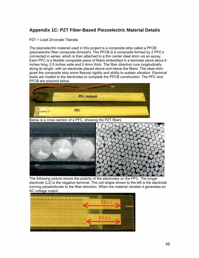
Appendix 1C: PZT Fiber-Based Piezoelectric Material Details PZT = Lead Zirconate Titanate The piezoelectric material used in this project is a composite strip called a PFCB (piezoelectric fiber composite bimorph). The PFCB is a composite formed by 2 PFC’s connected in series, which is then attached to a thin center steel shim via an epoxy. Each PFC is a flexible composite piece of fibers embedded in a laminate piece about 6 inches long, 0.5 inches wide and 0.4mm thick. The fiber direction runs longitudinally along its length, with an electrode placed above and below the fibers. The steel shim gives the composite strip some flexural rigidity and ability to sustain vibration. Electrical leads are riveted to the electrodes to complete the PFCB construction. The PFC and PFCB are pictured below.
Below is a cross section of a PFC, showing the PZT fibers.
The following picture s s the pola of the el rodes on the PFC. The longer
the ne tive termin The coil shape shown to the left is the electrodrunning perpendic er-direction. When the material vibrates it generates an AC voltage output
how rity ectelectrode (L2) is ga al. e
ular to the fib.
49

Appendix 2A: Electro-Mechanical Modeling
iezoelectric material develops electrical energy from mechanical input energy in e schematic below:
Pthe form of vibrations. See th
To generate electrical energy the piezoelectric material must be stimulated byeither constant input mechanical vibrations or an impulse that will cause the material to vibrate on its own. During this oscillation the material goes through repeated up and down displacement. The beam displacement causes changein mechanical stress in th
s e material which generates an output voltage.
Before the group was able to start power calculations, the mechanical vibrations of the system needed to characterized. Given the shape and material properties of the piezoelectric material the group treated the system as a vibrating cantilever beam. With the current floor tile design the material will be excited by the input force of a foot strike. When an individual steps on the tile, it will displace slightly. This small displacement will be enough to force the material to begin oscillating.
ver beam thes ease.
To begin modeling the behavior of the vibrating cantilever, the amplitude of the oscillations needed to be analyzed. The group calculated the stiffness coefficient, damping ratio, undamped natural frequency and damped natural frequency using the equations in the appendices. From the equation below the group was able to then characterize the amplitude of the tip of the beam on a time interval (t), given an initial displacement (Xo). Since the power output of the piezoelectric material is dependent on changing
litu e
(beam with a point mass). Analysis of the spring stiffness characteristics can be found in the material selection section of the mechanical model. When experimenting with applying a point mass to the piezoelectric material, the group made two observations: the lower the frequency of the vibration the longer the duration of the vibrations; and the lower the frequency the larger the amplitude of the vibration over the time interval. Using the frequency equations in the appendices the group was able to generate the graph below.
Because of natural damping effects inherent in a cantileoscillations will become smaller and smaller until they eventually c
e
)cos()2/(0 teXA d
tm ωζ ××= −
stress in the beam it is in the best interest of the group to maximize the ampand duration of the vibrations. These parameters are dependent on the dampingratio, which is dependent on spring stiffness and dimensions of the beam, and mass of the system
d
50

Natural Frequency vs. Mass
70.0
80.0
0.0
10.0
20.0
30.0
0 0.005 0.01 0.015 0.02 0.025 0.03
Mass (kg)
Nat
ural
Fr
40.0
50.0
60.0
eaqu
ency
(Hz)
Length 1 -> .15mLength 2 -> .18 mLength 3 -> .22 m
This graph demonstrates two relationships: as the point mass increases the natural frequency decreases; and as the length of the beam increases the natural frequency decreases. Increasing the length of the beam both changes the dimension of the beam (affecting the damping ratio) and increases the length between the mounting point of the beam and the location of the point mass. This confirmed the group’s initial conceptions that the beam should be as long aphysical dimension of the tile allow and that the point mass should be place
s the d on
the end of the beam. Next the group decided to explore the relationship between the mass of the point mass and amplitude of the vibrations. For this analysis we used the longest piece of material available from our supplier and varied the magnitude of the point mass at the end. The amplitude equation above was used to generate this following graph.
Beam Deflection vs. Time (point mass)
-0.03
Time (sec)
-0.02
-0.01
0
0.01
0.02
0.03
0.04
0 0.5 1 1.5 2 2.5 3
Tip
Def
lect
ion
(m)
Mass -> 0.0015Mass -> 0.011Mass -> 0.025
51
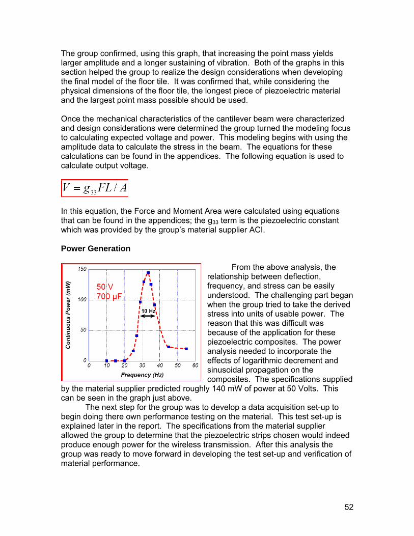
The group confirmed, using this graph, that increasing the point mass yields larger amplitude and a longer sustaining of vibration. Both of the graphs in this section helped the group to realize the design considerations when developing the final model of the floor tile. It was confirmed that, while considering the physical dimensions of the floor tile, the longest piece of piezoelectric material and the largest point mass possible should be used. Once the mechanical characteristics of the cantilever beam were characterized and design considerations were determined the group turned the modeling focus to calculating expected voltage and power. This modeling begins with using the amplitude data to calculate the stress in the beam. The equations for these calculations can be found in the appendices. The following equation is used to calculate output voltage.
In this equation, the Force and Moment Area were calculated using equations that can be found in the appendices; the g33 term is the piezoelectric constawhich was provided by the group’s material supplier ACI. Power Generation
nt
From the above analysis, the relationship between deflection,
gan ed
reason that this was difficult was because of the application for these piezoelectric composites. The power analysis needed to incorporate the effects of logarithmic decrement and sinusoidal propagation on the composites. The specifications supplied
by the material supplier predicted roughly 140 mW of power at 50 Volts. This can be seen in the graph just above. The next step for the group was to develop a data acquisition set-up to begin doing there own performance testing on the material. This test set-up is explained later in the report. The specifications from the material supplier allowed the group to determine that the piezoelectric strips chosen would indeed produce enough power for the wireless transmission. After this analysis the group was ready to move forward in developing the test set-up and verification of material performance.
frequency, and stress can be easily understood. The challenging part bewhen the group tried to take the derivstress into units of usable power. The
52

Appendix 2B: Initial Design Specifications
W e ig h t 2 .1 lbC o m p le te A s s e m b ly
D e s ig n S p e c if ic a t io n s
sL e n g th 1 f t
1 f tH e ig h t 2 inM a te r ia l o f C o n s tru c t io n L e x a nM a te r ia l T h ic k n e s s .1 in
d th 1 f t1 in
M o d u la r ity Y e s
L e n g thP o in t M a s sP o in t M a s s L o c a tio n
R e q u ire d P o w e r fo r T ra n s m itt io n S ta n d b y P o w e r
W id th 1 f tH e ig h t 3 in
L e n g th 1 f tW id th
M a te r ia l o f C o n s tru c t io n W o o d /F o a m ? !?L e n g th 1 f tW iH e ig h t
5 in.0 2 5 g
@ 4 .5 in
4 5 m W @ 3 .3 V1 m W
P ie z o e le c tr ic C o m p o s i
F lo o r T ile
S u b F lo o r
te S tr ip s
n s m it t io nE le c tr ic a l / W ire le s s T ra
53
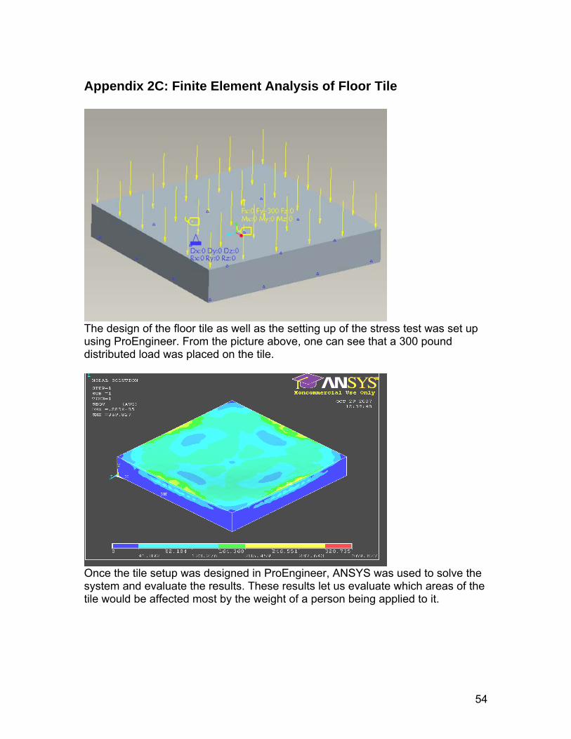
Appendix 2C: Finite Element Analysis of Floor Tile
The design of the floor tile as well as the setting up of the stress test was set up using ProEngineer. From the picture above, one can see that a 300 pound distributed load was placed on the tile.
Once the tile setup was designed in ProEngineer, ANSYS was used to solve the system and evaluate the results. These results let us evaluate which areas of the tile would be affected most by the weight of a person being applied to it.
54
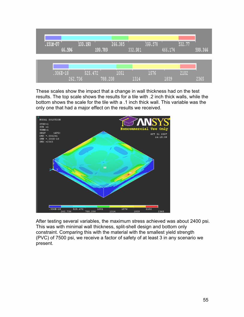
These scales show the impact that a change in wall thickness had on the test results. The top scale shows the results for a tile with .2 inch thick walls, while the bottom shows the scale for the tile with a .1 inch thick wall. This variable was the only one that had a major effect on the results we received.
After testing several variables, the maximum stress achieved was about 2400 psi. This was with minimal wall thickness, split-shell design and bottom only constraint. Comparing this with the material with the smallest yield strength (PVC) of 7500 psi, we receive a factor of safety of at least 3 in any scenario we present.
55

56
Appendix 2D: State of the Art The group used Google patent search to try to find piezoelectric floor tiles that have
een patented. The search returned no existing US patents for any form of power enerating or energy scavenging floor or floor components with piezoelectrics. It is
known that the piezoelectric concept and piezoelectric materials have been used for several years so the group decided to then expand the search to include prior research and prototyping of an energy scavenging floor utilizing piezoelectrics. What was found is that there are a number of universities and institutions that have experimented with using arious piezoelectric materials to produce prototype models of energy scavenging floor
The East Japan Railway company has installed ticket gates that use piezoelectric material to harness pressure and vibration caused by the foot traffic of passengers to power the gates themselves. This project has been successful in producing enough power to energize the ticket gates, but at this point they have not proven that it is cost effective to use this same technology elsewhere in the station to power lights or other electrical power draws.
MIT Sensate Floor
MIT has done a lot of development with piezoelectric materials. The floor tile in the picture is designed to sense the pressure of a person’s foot to track people movement. Most of MIT’s projects utilize piezoelectric polymers, this project included. MIT’s projects also use the sensing capabilities of
piezoelectrics, not the power generation characteristics. This Sensate Floor is similar to ours in that it tracks people movement, but it does not send the signal wirelessly, nor is it self-powering.
of PZT fiber-based composite materials produced by ACI. This material is able to generate ten times the amount of power of materials used in previous systems giving us a much higher potential for success. ACI is in the process of building a high production facility for manufacturing PZT fiber-based piezoelectrics which should greatly reduce the cost of this material, increasing the cost-effectiveness of the project. At this point in the project the group has also fully recognized that special attention needs to be paid to choosing the right application to utilize the low power characteristics of the material. This is why the group has chosen to use ultra-low power wireless transmission for our application.
bg
vsurfaces and floor mats. A small collection of these research projects can be found below.
East Japan Railway Company
These projects above prove that it is possible to convert previously-wasted mechanical energy from the movement of individuals into electrical energy through the use of piezoelectrics. However, these prior endeavors have had very limited success withregards to an appreciable amount of power generated and cost-effectiveness of theenergy harvesting system. A major advantage our project has over priors is the utilization

Appendix 3A: Spring Specifications
57

Appendix 3B: Mechanical Components Bill of Materials
Description Quantity Price
2 ft x 4 ft Lexan Plastic 1 $57.50
1 ft x 1 ft Lexan plastic 2 $23.22
Foam Selector Pack 1 $41.25
Corner Brackets 50 $17.00
Steel Nuts 100 $1.51
Steel Washers 100 $2.02
Epoxy Repair Cement 1 $11.41
Machine Screws 100 $8.06
Flexible Magnet Disks 20 $7.56
Ceramic Disc Magnets 20 $1.72
6" Heat Shrink Tubing 1 $2.52
Piezoelectric Strips 4 $240.00
7/8" Springs 4 $9.13
Quick Recovery Foam 1 $14.69
Polyurethane Foam 5 $19.30
Metal Shim Stock Assortment 1 $43.36
Aluminum Shim Stock 1 $4.25
Total $504.50
58

Appendix 3C: Full Pa M n ige odel of Fi al Des gn
Springs (4X)
Actuatio r Assem(Station
n Bablyary)
PZT St sripLexa
Sideweduce fr n)
nalls ictio
Aluminum Mounting
Block (r
Threaded Rod (4X)- controls height/spring
pre-load
Energy Harvesting
Circuit
¾” Woodard X)
Bo(2Allowable
Displacement (0<do<1.5”)
do
59

Appendix 4A: Full Circuit Diagram
The top row shows the four piezoelectric strips which are passed through individual rectifiers. The bottom left shows the combination of the piezoelectric outputs fed into the Energy Harvesting Module The output of the Energy Harvesting Module is fed into a PIC16F877a microcontroller in the 3.1 – 5.2V Range The microcontroller creates a USART signal reduced to 3.3V using resistors and fed into XBee transmitter The XBee receiver receives the data packet from the transmitter and outputs a “warning” sign using GUI on computer
60

Appendix 4B: Electrical Parts/Data Sheets/References Datasheet for PIC16F877A Microcontroller: http://ww1.microchip.com/downloads/en/DeviceDoc/30292c.pdf Datasheet for EH301 Energy Harvesting Module: http://www.aldinc.com/pdf/EH300ds.pdf Brochure for EH301 Energy Harvesting Module: http://www.aldinc.com/pdf/EH300Brochure.pdf Based on the final prototype the team has concluded the following electrical parts list necessary to completely build a working prototype. The cost of piematerials was graciously donated by the material supplier Advanced Cerametrics.
zoelectric
Electrical Parts List Reference: 1 www.advancedcerametrics.com/pages/energy_harvesting_components/http:// 2 www.radioshack.com/product/index.jsp?productId=2062581&cphttp:// 3 search.digikey.com/scripts/DkSearch/dksus.dll?Detail?name=923252-NDhttp:// 4 www.mpja.com/prodinfo.asp?number=4447+TEhttp:// 5 mouser.com/Search/ProductDetail.aspx?qs=NoieiqYAh1CVRGGWkhttp://www. RFRmg%3d%3d 6 microcontrollershop.com/product_info.php?cPath=112_184&products_id=http:// 992 7 www.radioshack.com/product/index.jsp?productId=2062324&cphttp:// 8 www.radioshack.com/product/index.jsp?productId=2062324&cphttp:// 9 www.digi.com/products/wireless/zigbee-mesh/xbee-series2-module.jsphttp://
61

62
Step
180 199 210
590 569 640
997 990 1080
1440 1490 154016 1550 1560 164017 1640 1650 178018 1710 1710 189019 1820 1800 198020 1950 1890 211021 2050 1980 221022 2110 2080 232023 2210 2220 239024 2260 2300 250025 2370 2400 261026 2430 2470 271027 2577 2590 281728 2671 2686 292129 2766 2782 302630 2860 2878 313031 2955 2973 323432 3049 3069 333833 3143 3165 3443
3238 3261 35473332 3356 3651
47 4466 4505 490248 4561 4601 500649 4655 4697 511050 4749 4793 521451 4844 4888 531952 4938 4984 542353 5033 5080 552754 5127 5176 563155 5222 5271 5736
mV/Step 94.47 95.76 104.23
4 Piezoelectric Strips
Appendix 5A: Detailed Test Results
no magnets 1 magnet 2 magnets1 97 94 12623 286 265 2954 405 370 3825 455 466 53367 725 630 7728 813 720 8529 926 872 942
1011 1080 1110 115012 1160 1220 123013 1240 1290 135014 1340 1390 142015
343536 3427 3452 375537 3521 3548 385938 3616 3644 396439 3710 3739 406840 3805 3835 417241 3899 3931 427642 3994 4027 438143 4088 4122 448544 4183 4218 458945 4277 4314 469346 4372 4410 4798
Voltage in 1000uF Cap (mV) Stepgnet 2 magnets
0.004 0.0082 0.016 0.020 0.0223 0.041 0.035 0.0444 0.082 0.068 0.0735 0.104 0.109 0.1426 0.174 0.162 0.2057 0.263 0.198 0.2988 0.330 0.259 0.3639 0.429 0.380 0.444
10 0.497 0.490 0.583
15 1.037 1.110 1.18616 1.201 1.217 1.34517 1.345 1.361 1.58418 1.462 1.462 1.78619 1.656 1.620 1.96020 1.901 1.786 2.22621 2.101 1.960 2.44222 2.226 2.163 2.69123 2.442 2.464 2.85624 2.554 2.645 3.12525 2.808 2.880 3.40626 2.952 3.050 3.67227 3.320 3.355 3.96828 3.567 3.607 4.26729 3.824 3.869 4.57730 4.090 4.140 4.89831 4.365 4.420 5.23032 4.648 4.709 5.57233 4.941 5.008 92634 5.242 5.316 29035 5.553 5.632 6.66536 5.872 5.958 7.051
293 7.448.638 7.856
91 8.27454 8.704
10.0577 8.896 10.530
9.305 11.0149.722 11.508
47 9.973 10.149 12.01448 10.399 10.585 12.53049 10.835 11.030 13.05750 11.279 11.485 13.59551 11.732 11.948 14.14452 12.194 12.421 14.70453 12.665 12.903 15.27554 13.145 13.394 15.85655 13.634 13.894 16.449
mJ/Step 0.248 0.253 0.299
4 Piezoelectric StripsEnergy in 1000uF Cap (mJ)
no magnets 1 ma1 0.005
11 0.583 0.616 0.66112 0.673 0.744 0.75613 0.769 0.832 0.91114 0.898 0.966 1.008
5.6.
37 6.200 6.37 638 6.5
39 6.883 6.940 7.238 7.341 7.602 7.726 9.144
9.59542 7.975 8.10757 8.49743 8.3
44 8.7445 9.14746 9.556

Gantt Charts
Phases I – III
63

Phases IV – VI One of the most iWithout a well th
mportant aspects of this project will be to have an effective and well defined project management plan. ought out plan for all aspects of the project it will become hard to complete all of the tasks in a timely and
fficient manner. There are many tasks throughout this project that will be dependent on other tasks in the project. Since this is the case, it is very important to hold true to the schedule for each task within this plan. If these tasks are not ompleted in the scheduled time frame it will create a domino effect that will holdup the project as a whole. In order to
define this schedule, the group used MS Project to create a Gantt chart that outlines each task that is required for completion of this stage of the project. This chart acts as an outline for the entire semester's work that is due for completion. In order to hold true to this schedule, one group member will act as a project manager, and thus delegate tasks and follow up upon completion to ensure good utilization of both time and resources. The Gantt Chart for the spring semester can be seen below.
Phase IV
e
c
ID Task Name Duration Start Finish
1 Phase IV 24 days Mon 1/21/08 Thu 2/21/082 Choose Components 3 days Mon 1/21/08 Wed 1/23/083 Place Order 1 day Wed 1/23/08 Wed 1/23/084 Finalize Design Drawings 3 days Wed 1/23/08 Fri 1/25/085 Build Initial Prototype in Machine Shop 5 days Mon 1/28/08 Fri 2/1/086 Develop Test Setup 15 days Mon 1/21/08 Fri 2/8/087 Updated Nugget Chart 1 day Tue 2/12/08 Tue 2/12/088 Write Written Report 1 5 days Fri 2/8/08 Thu 2/14/089 Prepare and Deliver Oral Report 1 5 days Fri 2/15/08 Thu 2/21/08
1/23
2/122/14
2/21
F S S M T W T F S S M T W T F S S M T W T F S S M T W T F S S M T W T F S S MJan 20, '08 Jan 27, '08 Feb 3, '08 Feb 10, '08 Feb 17, '08 Feb 24,
During phase IV of the design process the group progressed greatly. Within this time period, from the New Year until the present numerous key tasks were completed. The group was able to finalize the design, select components, order parts, and create fabrication drawings for the machinist. The group then spent numerous days in the machine shop to help the machinist fabricate the necessary parts needed for the complete manufacturing of the product. After the stage one prototype was built the group began to develop a testing setup for the prototype. Lastly, the group was able to update their Nugget Chart, write the progress report 1, and finally prepare for the progress presentation.
64

Phase V ID Task Name Duration Start Finish
10 Phase V 30 days Mon 2/18/08 Thu 3/27/0811 Develop Test Variables 2 days Fri 2/22/08 Mon 2/25/0812 Testing Period 1 4 days Tue 2/26/08 Fri 2/29/0813 Re-design cycle 1 3 days Sat 3/1/08 Tue 3/4/0814 Build Improved Prototype 2.5 days Wed 3/5/08 Fri 3/7/0815 Integrate Electrical Components 15 days Mon 2/18/08 Thu 3/6/0816 Aid Electrical Team with Electrical Design 10 days Tue 2/26/08 Fri 3/7/0817 Place Final Orders 1 day Sat 3/1/08 Sat 3/1/0818 Testing Period 2 5 days Tue 3/11/08 Mon 3/17/0819 Redesign Cycle 2 4 days Tue 3/18/08 Fri 3/21/0820 Design Website and upload E-Poster 2 days Thu 3/6/08 Fri 3/7/0821 Update Nugget Chart 1 day Wed 3/19/08 Wed 3/19/0822 Prepare and Deliver Oral Report 2 4 days Mon 3/24/08 Thu 3/27/08
3/1
3/193/27
F S S M T W T F S S M T W T F S S M T W T F S S M T W T F S S M T W T F S S M T W T F S S MFeb 17, '08 Feb 24, '08 Mar 2, '08 Mar 9, '08 Mar 16, '08 Mar 23, '08 Mar 30,
neral overview of these tasks can be seen in the above Gantt Chart. Some of these e multiple testing and redesigning periods, as this project will be an ongoing design process. Also, the group
plans to begin to work more in collaboration with the electrical engineering team in order to assist them in any development of specifications or sizing of components that might be needed. In addition, the group will require input from the EE team to efficiently select a pressure sensor for the monitoring application of the product. Phase VI
Looking ahead to phase V, the group was able to set realistic goals for milestone accomplishments to be completed during this phase of the project. Most of these tasks can be found in the section of the report which outlines the technical emphasis for this phase V. A getasks includ
ID Task Name Duration Start Finish
23 Phase VI 32 days Fri 3/28/08 Mon 5/12/0824 Testing Period 3 (Final Test) 11 days Fri 3/28/08 Fri 4/11/0825 Finalize Specifications 1 day Fri 4/11/08 Fri 4/11/0826 Assemble Final Prototype 5 days Mon 4/14/08 Fri 4/18/0827 Tw eak Prototype for Senior Design Day 2 days Mon 4/21/08 Tue 4/22/0828 Poster for Design Project Exhibition 5 days Mon 4/14/08 Fri 4/18/0829 Senior Design Day 1 day Wed 4/23/08 Wed 4/23/0830 Upload Project onto ME website 1 day Mon 4/28/08 Mon 4/28/0831 Share Prototype w ith Advanced Cerametric 5 days Thu 4/24/08 Wed 4/30/0832 Update Nugget Chart 1 day Wed 4/30/08 Wed 4/30/0833 Prepare and Deliver Final Report 4 days Mon 4/28/08 Thu 5/1/0834 Prepare and Deliver Final Presentation 5 days Fri 5/2/08 Thu 5/8/0835 Return Prototype to Senior Design Lab 1 day Mon 5/12/08 Mon 5/12/08
4/114/18
4/234/28
4/305/1
5/85/12
T W T F S S M T W T F S S M T W T F S S M T W T F S S M T W T F S S M T W T F S S M T W T F S S M T W'08 Mar 30, '08 Apr 6, '08 Apr 13, '08 Apr 20, '08 Apr 27, '08 May 4, '08 May 11, '08
Phase VI tasks will be dependent on the progress made during the previous phases, thus some of these tasks may hange over time, but the main goals and tasks will remain the same. c
65

Nugget Charts The following charts summarize the progress obtained during the six phases of project development which consist of the following: Phase I: Conceptual Design Phase II: Technical Analysis Phase III: Engineering Design
hase IV: Prototyping PPhase V: Experiment Design Phase VI: Performance Testing
66

Phase I Nugget Chart
o design and develop a unique commercial pplication.
• Project Objectives • Conceptual Designs and Highlights
2. Game or Toy 3. Sensing/Monitoring Application 4. Buoy Light or Ocean/Wave Application 5. Sports Device
Utilize the unique properties of PZT fiber-based piezoelectric materials t
1. Medical Device
a
• Why This Project and State-of-the-art and the use of advanced, fiber-
oelectric materials, proving the worthiness of this concept in new product markets. In general, many products in the current market:
• use piezoelectric transducers, not PZT fiber based materials
• do not utilize energy harvesting characteristics of piezoelectrics
• require energy input (e.g. internal battery) • do nothing with waste energy
• Drawing and Illustration of Promising Concepts Concept 1
This project is intended to expbased piez
• Key Issues/Problems to Solve 1. Acquire an analog to digital data acquisition system 2. Use Labview to determine the consistency of electrical
output, and also fatigue characteristics 3. Determine functional specification for auto-stiffening and
auto-powered knee brace 4. Determine a means of attaching material to knee brace 5. Look into damping / range limiting assembly
Piezoelectric strips -Sensing -Energy Harvesting
67
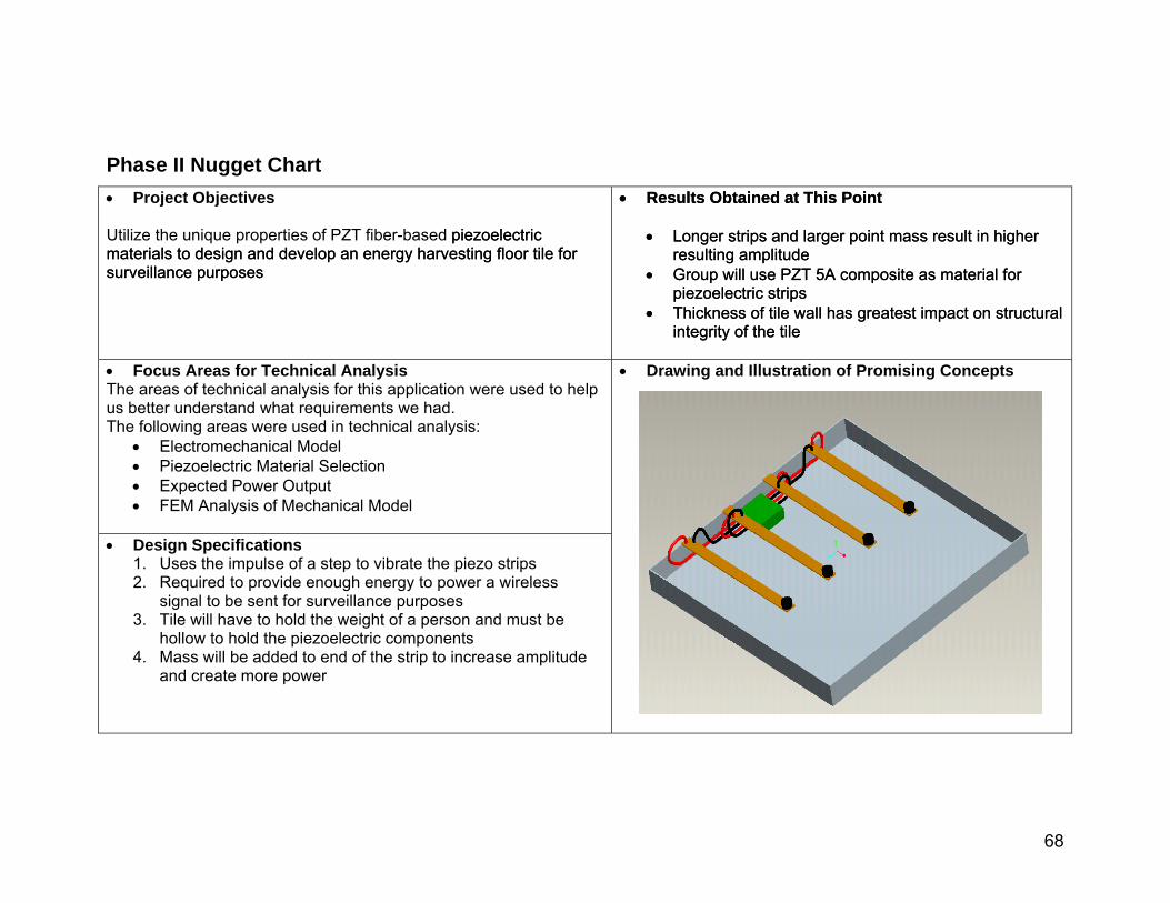
Phase II Nugget Chart • Project Objectives Utilize the unique properties of PZT fiber-based piezoelectric materials to design and develop an energy harvesting floor surveillance p
piezoelectric materials to design and develop an energy harvesting floor surveillance p
tile for urposes
higher
al for tile for
urposes
higher
al for
• Results Obtained at This Point • Results Obtained at This Point
• Longer strips and l• Longer strips and larger point mass rude
• Group will use PZT 5A composite as
arger point mass rude
• Group will use PZT 5A composite as
esult in
materipiezoelectric strips
esult in
materipiezoelectric strips
resulting amplitresulting amplit
• Thickness of tile • Thickness of tile wall has greatest impact on structural integrity of the tile
wall has greatest impact on structural integrity of the tile
• Focus Areas for Technical Analysis The areas of technical analysis for this application were used to helus better understand what requirements we had. The following areas were used in technical analysis:
• Electromechanical Model
p
• Piezoelectric Material Selection • Expected Power Output
FEM Analys• is of Mechanical Model
• Drawing and Illustration of Promising Concepts
• strips
Design Specifications 1. Uses the impulse of a step to vibrate the piezo 2. Required to provide enough ener
signal to be sent for surveillance purgy to power a wireless
poses f a person and must be
hollow to hold the piezoelectric components 4. Mass will be added to end of the strip to increase amplitude
3. Tile will have to hold the weight o
and create more power
68

Phase III Nugget Chart
y
erametrics Company to design and develop a floor tile that harvests energy from a foot strike.
the sole source of power to surveillance.
• Project Objectives
• Utilize the unique properties of PZT (lead zirconatetitanate) fiber-based piezoelectric materials developed bAdvanced C
• Use the harvested energy as transmit wireless signals for building
• Major Results Obtained this Semester
• Strategic Partnerships with ACI and EE Team Finalized Design, F
• EM Analysis, and ManufacturiAssembly Plan for floor tile concept Comp
ng
• letion of an A/D data acquisition system with interface to Labview via DAQ Card
• Finalized Design of Testing Apparatus
• From Technical Analysis to Engineering Design • Design Specifications were derived from the Technical
Analysis in Phase II for the entire system: o Floor Tile, Subfloor, Piez
Circuit, Wireless Transmoeleission
erative specifications will be finalize during
ctrics Strips, Electrical
design process, these design • Through testing and an itPhase IV
• Drawing and Illustration of Final Design
• Prototype Plan and Purchase Requisition 1. Purchase budgeted items from industrial suppliers (McM2
a
3
ster)
6. Program wireless controller using Zigbee Development Kit 7. Purchase wireless transmitter and receiver 8. Finalize energy harvesting circuitry
. Custom fabricate parts in machine shop. Co-assemble floor tile prototype and testing apparatus. .
4. Perform extensive testing on prototype according to test variables.
5. Optimize the current design based on testing results in an iterative design process.
69

Phase IV Nugget Chart • Project Objectives
• Utilize the unique properties of PZT (lead zirconate titanate) fiber-based piezoelectric materials developed by Advanced Cerametrics Company to design and develop a floor tile that harvests energy from a foot strike.
• Use the harvested energy as the sole source of power to transmit wireless signals for building surveillance.
•
• i• u
Pol• Com
Major Results Obtained this Semester • Protototype tile has been fabricated
P ezoelectric Strip Fabrication process developed S bfloor materials limited to Silicone, EVA,
yurethane pletion of an A/D data acquisition system with
in erface to Labview via DAQ Card t• eT st and Data Processing Plan developed
• •From Engineering Design to Prototype Development Perform extensive testing on prototype according to test
variables. • Optimize the current design based on testing results in a
iter v
n ati e design process. gr m wireless controller using Zigbee Development Kit • Pro a
• Finalize energy harvesting circuitry
•
Drawing and Illustration of Final Design/Prototype
• ro.
Express
P1
totype Testing / Optimization Generate Voltage vs. Time graph in Labview Signal
2. Export data to Excel for post-processing 3. Calculate the logarithmic decrement 4. Multiply the Voltage values by 8.33 to back-calculate
actual voltage (because of voltage divider network. 5. Calculate energy per footstrike 6. Calculate # footstrikes to charge capacitive network
(values not yet determined but is estimated to be roughly 0.25 to 0.5 Farad)
7. Judge the feasibility of the test condition
70

71
Phase VI Nugget Chart
ee lPiezoelectric SurvPiezoelectric Surv illance Floor Tileil ance Floor Tile
Springs (4X)
Actuation Bar Assembly(Stationary)
PZT StripsAluminum Mounting
ockBl
Thre ed Rod ad(4X)- controls height/spring
e-lpr oad
LexanSidewalls
(reduce friction)
E rgy esting
neHar
C uitvirc
¾” Wood Board (2X)Allowable
cement Displa(0<d <1.5”)o
do
Stored Voltage vs. # of steps
01000200030004000500060007000
0 10 20 30 40 50 60
# of steps
Volta
ge (m
V), 1
000u
F ca
p
no magnets
1 magnet
2 magnets
Upper VoltageThreshold
Lower VoltageThreshold
8.3mJ useful ener gy