performance of a mohos-type memory using hfo nanoparticles ... molina/5_2013e... · performance of...
TRANSCRIPT

Performance of a MOHOS-type Memory Using HfO2 nanoparticles as Charge Trapping Layer and Ultra-Thin Tunneling Oxide Thickness
Joel Molina1*, Carlos Zuniga1, Edmundo A. Gutierrez1, Wilfrido Calleja1, Pedro Rosales1, Francisco J. Hidalga1 and Alfonso Torres1
1 National Institute of Astrophysics, Optics and Electronics, Electronics Department. Tonantzintla, Puebla 72000. Mexico. * Corresponding author: Fax: 52-222-2470517, E-mail: [email protected]
In this work, we use HfO2 nanoparticles (np-HfO2, embedded in a spin-on glass SOG oxide matrix) as charge trapping layer (CTL) in Metal/Oxide/High-κ/Oxide/Silicon (MOHOS)-type non-volatile memory structures. By depositing the same CTL on an ultra-thin layer of chemical oxide (SiOx ≤ 2 nm), a distinctive trade-off is observed in both writing/erasing and data retention time characteristics when different thicknesses are used for the tunneling oxide. Specifically, better writing/erasing times are obtained while the data retention characteristics worsen when the tunneling oxide thickness decreases to less than 2 nm. The best memory performance is obtained for a CTL (∼120nm, based on np-HfO2) deposited on a tunneling oxide of 1.5nm < SiOx < 2nm. Key words: MOHOS memory, tunneling oxide, HfO2 nanoparticles, high-k, charge trapping
1. INTRODUCTION After replacing the floating gate (polysilicon-based) by a nitride-based trapping layer in flash memories, great improvements have been obtained in terms of enhanced data endurance and moderate scaling for these memory devices [1-2]. On the other hand, by using ultra-thin tunneling oxides in SONOS (Silicon-Oxide- Nitride-Oxide-Silicon) memories, efficient scaling down for these devices is restrained because of the high levels of gate leakage current that result in poor data retention times. To reduce leakage currents from tunneling back to the substrate, thicker tunneling oxide thickness are needed for the memory structures but this limits an efficient programming (writing/erasing) since lower charge densities are trapped at the defect-based energy levels of their active layers. In order to compensate both programming and data retention time problems, we propose a memory structure in which the CTL is based on HfO2 nanoparticles deposited on ultra-thin chemical oxides of variable thickness. By using np-HfO2, we can increase the dielectric constant of the CTL as well as the concentration of their defect-based energy levels available for charge trapping (np-HfO2 present a high contact surface area compared to a thin film of the same material). Because of the high dielectric constant for this CTL, higher charge densities Qinj can be injected from the substrate using the same electric fields (enhancing programming characteristics) while giving some space to increase the tunneling oxide thickness and therefore, enhance the data retention times simultaneously. 2. EXPERIMENTAL For all experiments, we have used silicate-type SOG materials (from Filmtronics, Corp., 15A), N-type silicon wafers (100) with resistivity of 5–10 Ω·cm, and np-HfO2 (99.9% purity from American Elements) having granular diameter of 98nm (average, measured by Dynamic-Light Scaterring after sonication). Standard RCA cleaning was applied to all wafers and then dipped in HF solutions so that HF-last surfaces were obtained. The oxide stack
fabrication was realized sequentially thus obtaining 1) an ultra-thin direct-tunneling chemical oxide SiOx, 2) a high-k CTL based on np-HfO2 and 3) a thick blocking SOG-based oxide SiO2. The tunneling oxide was formed by immersion of the HF-last silicon wafers (Si-H) into H2O2 at 75°C by 4, 16 and 32 min so that three different SiOx thicknesses were obtained, see figure 1.
Fig. 1.- Tunnneling oxide SiOx thickness vs. immersion time in hot H2O2. SiOx ≤ 2nm (after ellipsometry measurements) can be used for the MOHOS memory. A CTL based on np-HfO2 was obtained by preparing a np-HfO2:H2O:CH3COOH:SOG solution in which the concentration ratio of np-HfO2 to SOG was 30 wt% (300 mg/mL). The solute concentration was measured with an analytical balance AG285 from Mettler-Toledo. These np-HfO2 were then hydrolyzed in the SOG solutions by using water bath treatments (baine marie, 80°C, 2 h) in order to obtain homogeneous solution mixtures. The final np-HfO2:SOG solutions were then directly applied on the wafers' surfaces and spinned at 7000 rpm by 20 sec. After np-HfO2:SOG application, all films were initially baked at 200°C (10 min in N2 ambient) in order to evaporate most of the organic solvents. A second thermal treatment of 1000°C (30 min in N2) was also
569
Trans. Mat. Res. Soc. Japan 38[4] 569-572 (2013)
performed within a quartz furnace so that better film densification and solvent removal could be obtained after this final curing process. The blocking oxide SiO2 was also formed by direct deposition of a silicate SOG solution on the wafer surface and spinned at 7000 rpm by 20 sec. This last dielectric film was also baked at 200°C (10 min in N2) and 1000°C (30 min in N2) so that the former oxide films are covered with this thicker blocking oxide. The thicknesses for all oxide films were measured with a Gaertner ellipsometer L117 and a Tencor alpha-step equipment. The average thickness for the blocking and trapping oxide layers is 130 and 120 nm respectively. For electrical C–V and I–V characterization, all oxide films were metalized with 1 μm of aluminum by evaporation and unless otherwise stated, a gate capacitor area of 13.34e–4 cm2 was used for all MOHOS devices. Following metallization, a last thermal treatment (450°C in forming gas ambient, 5% H2 + 95% N2) was applied to all samples. All films' chemical compositional analysis was obtained by Fourier-Transform InfraRed (FTIR) spectroscopy in absorbance mode with a Bruker Vector-22 system. Finally, C–V and I–V measurements were done by using a Keihtley Model 82-DOS Simultaneous C–V system and an HP 4156B Semiconductor Parameter Analyzer respectively. 3. RESULTS AND DISCUSSION Figure 2 shows the FTIR spectrum of an HfO2/SiOx/ Si stacked structure after thermal treatment. We notice the characteristic absorption peaks for some common Si-O and Hf-O chemical bonds, thus confirming proper inclusion of the np-HfO2 in the CTL. These two Hf-O chemical bonds are detected at 752 cm-1 and 515 cm-1 and whose peak intensity increase directly with the concentration of np-HfO2 [3-4].
Fig. 2.- FTIR spectrum (absorbance mode) for the CTL based on np-HfO2. Besides the typical absorbance peaks for Si-O bonds, two distinctive absorbance peaks related to Hf-O chemical bonds are also detected [3-4]. Figure 3 shows the full I-V characteristics for a MOHOS structure (having a SiOx= 2nm) and we notice that a wide conduction window is formed after reaching the breakdown voltage of Vbkd ~3V. Since all MOHOS devices reach almost the same Vbkd, we took care to inject enough electronic charge using a gate voltage Vg just below Vbkd. Considering this large conductivity window between the low/high conduction states of about 5 orders of magnitude, we think there is plenty of room
to inject large densities of electronic charge Qinj at the CTL in order to properly modulate Vfb/Vth in memory devices without needing to overstress the stacked oxide using any Hot-Carrier Injection (HCI) mechanism. After breakdown, the electronic conduction properties of the memory device are quite similar to those of a metal/ semiconductor rectifying contact, which makes sense if one considers the existence of a conductive filamentary path connecting both the silicon substrate to the aluminum metal gate. Figure 4 shows that after injecting a small density of negative charge during an initial writing procedure (electrons being injected from the substrate into the CTL by a Fowler-Nordheim injection mechanism), its flat-band voltage shifts by ΔVfb~ 0.25V (the figure shows all fresh, writing and erasing conditions). The erasing procedure shifts back the Vfb close to its original state. On the other hand, it is important to notice that both writing/erasing conditions were applied on this memory without using any HCI mechanism, but only a relatively small electric field, quite important to enhance the reliability of the device.
Fig. 3.- I-V characteristics for a MOHOS memory. After dielectric breakdown, a wide memory window can be observed between the low-high current levels (arrows 1-2). This memory window is used for charge injection from the substrate into the CTL just before breakdown.
Fig. 4.- C-V characteristics for a MOHOS memory. After an initial charge injection procedure (writing), a ΔVfb∼0.25V is obtained compared to its fresh condition. Figures 5(a-b) show the memory performance in terms on ΔVfb vs. programming time (writing/erasing conditions) at Vg= ±2V and using different SiOx thicknesses. Higher ΔVfb is obtained for writing/erasing conditions in structures having the thinner SiOx as
570 Performance of a MOHOS-type Memory Using HfO2 nanoparticles as Charge Trapping Layer and Ultra-Thin Tunneling Oxide Thickness
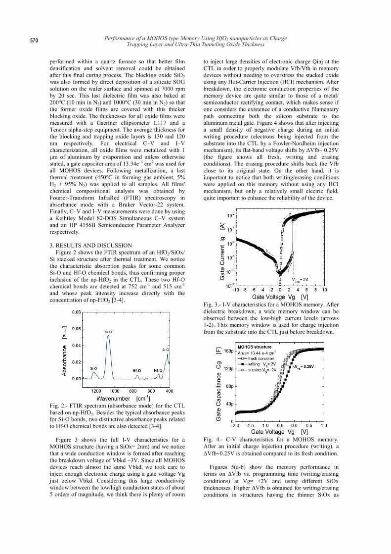
expected. Charge was injected into the trapping layer using a Fowler-Nordheim (F-N) conduction mechanism and without using any hot-carrier injection mechanism, thus promoting an enhanced reliability for these memory devices. Also, it is worth noticing that the erasing condition does not recover completely the Vfb originally shifted. It is possible that the existence of deep-trap levels for carriers in the trapping layer may cause an incomplete recovery of Vfb. This parasitic effect is observed for all samples in the erasing condition and worsens for thicker SiOx. If present, these deep-trap levels for injected carriers would make more difficult to annihilate the initially trapped electrons within the CTL or to excite these trapped electrons back to the conduction band. The later is also observed when the MOHOS structures are annealed at low temperatures [5].
Fig. 5.- (a) Writing characteristics using ΔVfb vs. writing time. Larger ΔVfb is obtained for the MOHOS memories having the thinnest tunneling SiOx oxide. (b) Erasing characteristics using ΔVfb vs. erasing time. MOHOS memories with the thinnest SiOx (thickness of 1.2 nm) are erased more effectively. On the other hand, given that the writing/erasing speed operations are usually flat-band/threshold voltage (Vfb/Vth) shift vs time plots and that they are measured in terms of the applied gate voltage, having thinner oxide stacks (including all blocking/trapping/tunneling oxides) would increase the current density being injected to the trapping layer and thus, a lower operating voltage would be needed to shift Vfb/Vth in any particular direction. This effect could be mistakenly interpreted as a higher efficiency of the high-k layer to trap charge since lower operating gate voltages are needed. By integrating the injected gate current density Jg with time,
we are able to quantize the effective density of charge being injected at the memory device:
𝑄𝑄𝑄𝑄𝑄𝑄𝑄𝑄 = ∫ 𝐽𝐽𝐽𝐽 𝑑𝑑𝑑𝑑𝑡𝑡0 (1)
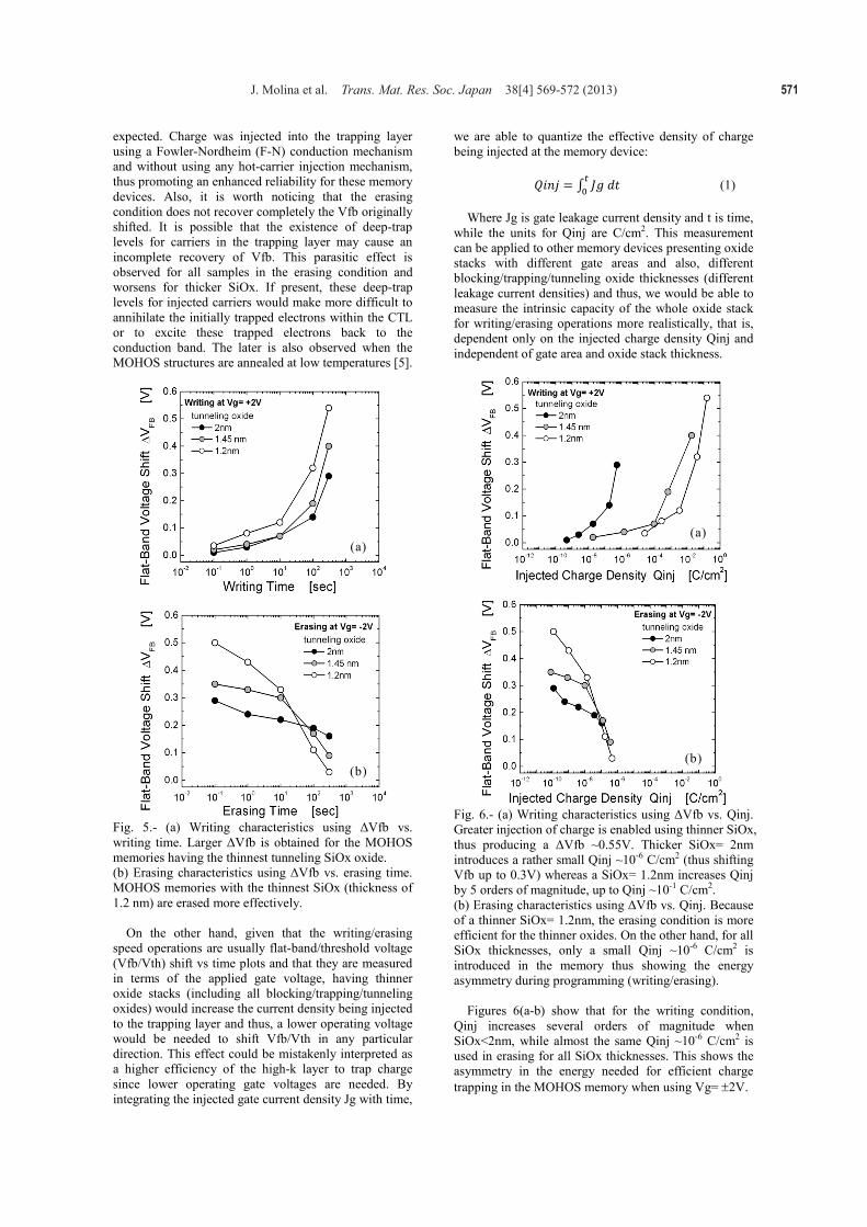
Where Jg is gate leakage current density and t is time, while the units for Qinj are C/cm2. This measurement can be applied to other memory devices presenting oxide stacks with different gate areas and also, different blocking/trapping/tunneling oxide thicknesses (different leakage current densities) and thus, we would be able to measure the intrinsic capacity of the whole oxide stack for writing/erasing operations more realistically, that is, dependent only on the injected charge density Qinj and independent of gate area and oxide stack thickness.
Fig. 6.- (a) Writing characteristics using ΔVfb vs. Qinj. Greater injection of charge is enabled using thinner SiOx, thus producing a ΔVfb ~0.55V. Thicker SiOx= 2nm introduces a rather small Qinj ~10-6 C/cm2 (thus shifting Vfb up to 0.3V) whereas a SiOx= 1.2nm increases Qinj by 5 orders of magnitude, up to Qinj ~10-1 C/cm2. (b) Erasing characteristics using ΔVfb vs. Qinj. Because of a thinner SiOx= 1.2nm, the erasing condition is more efficient for the thinner oxides. On the other hand, for all SiOx thicknesses, only a small Qinj ~10-6 C/cm2 is introduced in the memory thus showing the energy asymmetry during programming (writing/erasing). Figures 6(a-b) show that for the writing condition, Qinj increases several orders of magnitude when SiOx<2nm, while almost the same Qinj ~10-6 C/cm2 is used in erasing for all SiOx thicknesses. This shows the asymmetry in the energy needed for efficient charge trapping in the MOHOS memory when using Vg= ±2V.
(a)
(b)
(a)
(b)
571J. Molina et al. Trans. Mat. Res. Soc. Japan 38[4] 569-572 (2013)

The conduction and valence band off-sets of the silicon substrate with respect to the tunneling oxide SiOx, the CTL based on np-HfO2 and the thicker blocking oxide SiO2 are well characterized [6-7] and they present the following idealized energy band diagram, see figure 7.
Fig. 7.- Idealized energy band diagram for the MOHOS memory structure (showing an uniform HfO2 film in the CTL for clarity purposes). The energy conduction and valence band-offsets are also shown for reference [6-7]. The previous energy diagram is important because, whether using the measurement scheme of figures 5(a-b) or figures 6(a-b), the programming operations for this memory device would follow the same physical mechanisms for electron/hole trapping. During writing conditions, electrons accumulate at the substrate's surface and they gain enough energy from the applied gate voltage Vg enabling them to cross the tunneling oxide's energy barrier with energies well below 3.1eV (the tunneling oxide is thin enough and electrons can tunnel directly) and be trapped at the np-HfO2 trapping layer, thus shifting Vfb to positive values. During erasing conditions, a negative gate voltage inverts the silicon surface thus increasing the hole density and because of the electric field, these holes are trapped at the np-HfO2 layer (where they could annihilate some already trapped electrons), thus shifting Vfb to negative values. The former process would occur after the holes are able to tunnel through the thin tunneling oxide and also have enough energy, well below 3.1eV (valence band offset), to be trapped at the np-HfO2 trapping layer. Figure 8 shows the data retention time for the MOHOS memory using different tunneling oxide SiOx thicknesses. The writing condition used was Vg= +2V for the longest time as shown in figure 5(a). Similarly to the programming conditions (writing/erasing), the data retention time was measured right after charge injection in order to avoid any possible discharge of the trapped carriers via the electric circuit that is used during measurement. We notice that almost 80% of the charge is retained using thicker SiOx while the charge decays almost linearly with time for thinner SiOx. The best trade-off for better programming (both writing/erasing conditions) and enhanced data retention time, is found for a tunneling oxide thickness of 1.5nm<SiOx<2nm. By comparing figures 5(a-b) and figure 8, we can notice the intrinsic trade-off between programming time (writing/ erasing condition) and data retention time when using different tunneling oxide SiOx thicknesses. Finally, even though the programming times are rather slow in our
MOHOS-type memories, we have shown that after injecting very small charge densities Qinj≤ 10−2 C/cm2 into the gate oxides (without using any HCI mechanism), proper modulation of Vfb can be achieved so that the final reliability of these devices is expected to increase.
Fig. 8.- Data retention time characteristics for the MOHOS memory after initial charge trapping (writing condition). For the thinner SiOx thicknesses, trapped carriers are able to tunnel back to the silicon substrate having almost a linear decay with time. For a SiOx= 2nm, charge is retained at 80% of its original ΔVfb. 4. CONCLUSIONS By using a simple and low-cost spin-coating method for the charge trapping layer (based on np-HfO2) of a novel MOHOS memory device, wide current memory windows have been obtained in MOHOS memories and their charge-trapping characteristics (programming and data retention times) are strongly correlated to the tunneling SiOx thickness. The best trade-off for the whole memory performance is obtained for a CTL (based on np-HfO2) deposited on a tunneling oxide of 1.5nm < SiOx < 2nm in thickness and whose memory operation can be done without using HCI mechanism.
ACKNOWLEDGMENTS This work was fully supported by the National Council of Science and Technology (CONACyT- Mexico).
REFERENCES [1] F.R. Libsch, M.H. White, in: W.D. Brown, J.E. Brewer (Eds.), IEEE Press Series on Microelectronic Systems, 1997, pp. 309–357. [2] J. Bu, M.H. White, Solid-State Electron. 45 (1) (1995) 113–120. [3] Frank M, Sayan S, Dormann S, Emge TJ, Wielunski LS, Garfunkel E, Chabal YJ (2004) Mater Sci Eng B 109, pp. 6-10. [4] J. Molina, A.L. Munoz, W. Calleja, P. Rosales and A. Torres, J. Mater. Sci. (2012) 47:2248–2255. [5] J. Molina, R. Ortega, W. Calleja, P. Rosales, C. Zuniga and A. Torres, (2012) Mater Sci Eng B 177, pp. 1501-1508. [6] Y.N. Tan, W.K. Chim, B.J. Cho, W.K. Choi, IEEE Trans. Electron Dev. 51 (7) (2004) 1143–1147. [7] H.C. You, T.H. Hsu, F.H. Ko, J.W. Huang, W.L. Yang, T.F. Lei, IEEE Electron Dev. Lett. 27 (8) (2006) 653–655.
572
(Received February 22, 2013; Accepted August 9, 2013)
Performance of a MOHOS-type Memory Using HfO2 nanoparticles as Charge Trapping Layer and Ultra-Thin Tunneling Oxide Thickness