philips technical revie technical review dealing with technical problems relating to the products,...
TRANSCRIPT
· VOLUME 22, 1960/61, No. 7 pp. 217-244 Published 5th April 1961
Philips Technical ReviewDEALING WITH TECHNICAL PROBLEMS
RELATING TO THE PRODUCTS, PROCESSES AND INVESTIGATIONS OFTHE PHILIPS INDUSTRIES
PROPERTIES AND APPLICATIONS OF INDIUM ANTIMONIDE
by R. E. J. KING*) and B. E. BARTLETT*).
The increasing demand for photoconductive cells which extend their sensitivity range intothe far infra-red, has led to the construction of two new photocells based on crystals of indiumantimonide.
In this article the preparatien of InSb crystals and the construction and performance ofphotocells based on InSb are described. Mention is also made of the use of InSb in Hall gener-ators. These and other devices will be discussed in a forthcoming article in this journal.
In recent years a search has becn made for semi-conductors to supplement silicon and germaniumfor use in electronic applications. Since no otherelements appear particularly useful, interest hasbeen focussed on compounds. Most work has beendone on compounds of elements from group IIIand V of the periodic table, such as GaAs, GaP,InSb, etc. Of these compounds, indium antimonidehas been studied most intensively 1), because itsproperties make it particularly suitable for a numberof applications. In addition, the problems involvedin the preparation of InSb are more tractable thanthose encountered with other, similar, compounds.Photocells, Hall generators and other devices basedon InSb are already being manufactured by anumber of factories, amongst others the Mullarddivision at Southampton.
Properties of !nSb
Optical and electrical properties
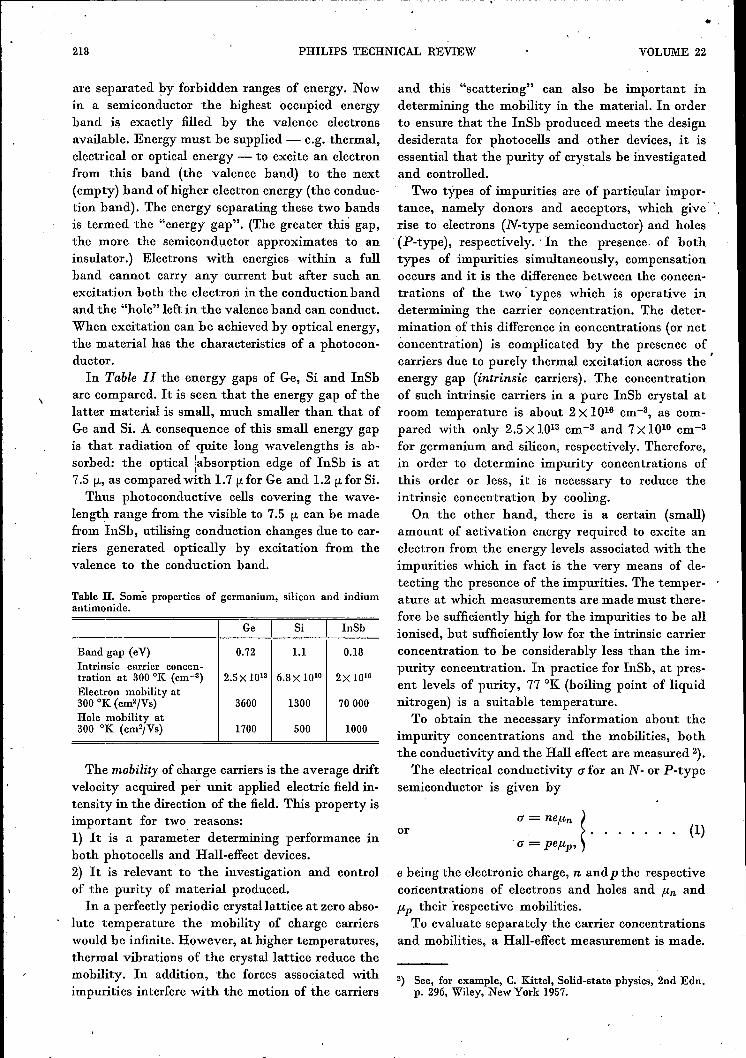
In Table I is shown part of the periodic table ofthe elements. The elements within the columns ofthe table have roughly similar chemical propertiesbecause they have the same number of outer shellvalency electrons.
*) Mullard Radio Valve Co., Southampton Works.1) A. N. Blum, N. P. Mokrovski and A. R. Regel, J. tech.
Phys. (Moscow) 21, 237, 1951; H. Welker, Z. Naturf. 7a,744, 1952 and 8a, 248, 1953; R. Gremmelmaier and O.Madelung, Z. Naturf. 8a, 333, 1953; H. Weiss, Z. Naturf.8a, 463, 1953.
546.682.'86
The elements in column IVA, with the exceptionof lead, are found to be semiconductors and crystal-lise in the diamond configuration by forming fourtetrahedral bonds. InSb forms the same type of
Table J. Groups lIla, IVaand Va of the periodictable of elements.
IIIA KA JZ'A
B C N5 6 7
Al Si P13 14 15
Ga Ge As
31 32 33
In Sn Sb49 50 51
Tl Pb Bi
81 82 834114
structure utilising the three valence electrons ofindium and the five of antimony to give the fourbonds. Consequently the electrical and optical prop-erties of the material are qualitatively similarto those of germanium and silicon. However, themagnitudes of the important parameters underlyingthe physical properties of the bulk material are dif-ferent.Two important quantities which affect the optical
and electrical properties of the material are the 'energy gap and the mobility of the charge carriers.These will now be considered.In solids there are bands of permissible energies
for electrons in contrast to the discrete electron ener-gy leeels permissible in separate atoms. These bands
•218 PHILIPS TECHNICAL REVIEW VOLUME 22
are separated by forbidden ranges of energy. Nowin a semieonduetor the highest occupied energyband is exactly filled by the valence electronsavailable. Energy must be supplied - e.g. thermal,electrical or optical energy - to excite an electronfrom this band (the valence band) to the next(empty) band of higher electron energy (the conduc-tion band). The energy separating these two bandsis termed the "energy gap". (The greater this gap,the more the semiconductor approximates to aninsulator.) Eleetrons with energies within a fullband cannot carry any current but after such anexcitation both the electron in the conduction bandand the "hole" left in the valenee band can conduct.When excitation can be achieved by optical energy,the material has the characteristics of a photocon-ductor.In Table IJ the energy gaps of Ge, Si and InSb
are compared. It is seen that the energy gap of thelatter material is small, much smaller than that ofGe and Si. A consequence of this small energy gapis that radiation of quite long wavelengths is ab-sorbed: the optical !absorption edge of InSb is at7.5 !L, as compared with 1.7 !L for Ge and 1.2 !L for Si.Thus photoconductive cells covering the wave-
length range from the visible to 7.5 !L can be madefrom InSb, utilising conduction changes due to car-riers generated optically by excitation from thevalence to the conduction band.
Table 11. Some properties of germanium, silicon and indiumantimonide.
Ge Si InSb
Band gap (eV) 0.72 1.1 0.18Intrinsic carrier concen-tration at 300 "K (cm-3) 2.5X 10¹³ 6.8 X 10¹⁰ 2X 10¹⁶Electron mobilityat300 OK (cm2JVs) 3600 1300 70000Hole mobility at300 OK (cm2/Vs) 1700 500 1000
The mobility of charge carriers is the average driftvelocity acquired per unit applied electric field in-tensity in the direction of the field. This property isimportant for two, reasons:1) It is a parameter determining performance inboth photocells and Hall-effect devices.2) It is relevant to the investigation and controlof the purity of material produced.In a perfectly periodic crystallattice at zero abso-
lute temperature the mobility of charge carrierswould be infinite. However, at higher temperatures,thermal vibrations of the crystallattice reduce themobility. In addition, the forces associated withimpurities interfere with the motion of the carriers
and this "scattering" can also be important indetermining the mobility in the material. In orderto ensure that the InSb produced meets the designdesiderata for photocells and other devices, it isessential that the purity of crystals be investigatedand controlled.Two types of impurities are of particular impor-
tance, namely donors and acceptors, which giverise to electrons (N-type semiconductor) and holes(P-type), respectively .. In the presence. of bothtypes of impurities simultaneously, compensationoccurs and it is the difference between the concen-trations of the two' types which is operative indetermining the carrier concentration. The deter-mination of this difference in concentrations (or netconcentration) is complicated by the presence ofcarriers due to purely thermal excitation across theenergy gap (intrinsic carriers). The concentrationof such intrinsic carriers in a pure InSb crystal atroom temperature is about 2 X 1016 cm-3, as com-pared with only 2.5 X 1013 cm-3 and 7 X 1010 cm-3
for germanium and silicon, respectively. Therefore,in order to determine impurity concentrations ofthis order or less, it is necessary to reduce theintrinsic concentration by cooling.
On the other hand, there is a certain (small)amount of activation energy required to excite anelectron from the energy levels associated with theimpurities which in fact is the very means of de-tecting the presence of the impurities. The temper-ature at which measurements are made must there-fore be sufficiently high for the impurities to he allionised, but sufficiently low for the intrinsic carrierconcentration to be considerably less than the im-purity concentration. In practice for Inêb, at pres-ent levels of purity, 77 OK (boiling point of liquidnitrogen) is a suitable temperature.
To obtain the necessary information about theimpurity concentrations and the mobilities, boththe conductivity and the Hall effect are measured 2).
The electrical conductivity 0' for an N- or P-typesemiconductor is given by
or0' = nefln ~.
, 0' = peflp' ~(1)
e being the electronic charge, nand p the respectiveconcentrations of electrons and holes and fln andflp their respective mobilities.
To evaluate separately the carrier concentrationsand mobilities, a Hall-effect measurement is made.
2) See, for example, C. Kittel, Solid-state physics, 2nd Edn.p. 296, Wiley, NewYork 1957.
1960/61,No. '7 PROPERTIES AND APPLICATIONS OF INDIUM ANTIMONIDE
The Hall effect may be illustrated with the aidof fig. 1.H a current I is passed along a rectangular speci-
men and a magnetic field B is applied at right-angles
I~
Fig. 1. The Hall effect. B is the induction of the appliedmagnetic field, I the current through the specimen of thick-ness d. Al and A2 are the Hall-voltage contacts.
to the direction of current flow, then a potentialdifference is established in a direction perpendicu-lar to both the field and the current directions, Ifcontacts are made on the specimen at Al and A2
this potential difference known as the Hall voltage,can be measured. The open-circuit Hall voltageVHois given by the equation,
RHIBVHo=-d-'
where d is the thickness of the specimen in the di-rection of the magnetic field. For a particular tem-perature RH is a constant of the material and isknown as the Hall coefficient. The above equationassumes that the ratio of length to breadth of thespecimen is considerable greater than unity.
For an N- or P-type semiconductor, the Hallcoefficient is:
or
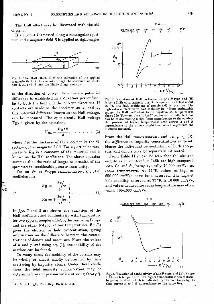
In figs. 2 and 3 are shown the variation of theHall coefficient and conductivity with temporaturefor two typical samples ofInSb, the one being P-typeand the other N-type, at low temperatures. Eq. (3)gives the electron or hole concentration, givinginformation on the difference between the concen-trations of donors and acceptors. From the valuesof nand p and using eq. (1), the mobility of thecarriers can be found.In many cases, the mobility of the carriers may
be wholly or almost wholly determined by theirscattering by impurity atoms. Under these condi-tions the total impurity concentration may bedetermined by comparison with scattering theory 3).
3) R. B. Dingle, Phil. Mag. 46, 831, 1955:
T-oo 1000500 300 200 150 120 100 BOoK~~~~~~~r--T~~----~
102~~~~~-*~~~~~~~~~o I 2 3 4 5 6 7 8 9 10 11 12
-IOYr,°K)
+ A
»=:':
219
4110
Fig. 2. Variation of Hall coefficient of (A) P-type and (B)N-type InSb with temperature. At temperatures below about160oK the Hall coefficient of sample (A) is positive. Thehigh ratio of electron to hole mobility in indium antimonidecauses the Hall coefficient to be negative at temperaturesabove 160OK when it is a "mixed" conductor i.e. both electrdnsand holes are making a significant contribution to the conduc-tion process. At higher temperatures both curves A and Bapproximate to the same straight line, which represents theintrinsic material.
(2)From the Hall measurements, and using eq. (3),the difference in impurity concentrations is found.Hence the individual concentration of both accep-tors and donors may be separately estimated.
From Table II it can be seen that the electronmobilities encountered in InSb are high comparedwith Ge and Si, being typically 70 000 cm2fVs atroom temperature. At 77 0l( values as high as650000 cm2fVs have been observed. The highesthole mobility observed at 77 0l( is 10000 cm2fVs,and values deduced for room temperature may oftenreach 700-1000 cm2fVs.
T_
oo 1000 500 300 200 150 120 100 80 "«
(3)
103_Q-I -Icm
A
100 I 2 3 4 5 6 7 8 9 10 n U- 103/fOK) 4111
Fig. 3. Variation of conductivity of (A) P-type and (B) N-typeInSb with temperature. For higher temperatures the materialbecomes intrinsic which is indicated by the fact (as in fig. 2)that curves A and B approximate to the same line.

220 PHILlPS TECHNICAL REVIEW VOLUME 22
A consequence of thèse high mobilities is thatInSb displays large magnetoresistance effects 4).A further consequence is that the power efficiencyof Hall generators made from InSb is high com-pared with similar devices manufactured from Geor Si.
Recombination and trapping
Non-equilibrium carrier concentrations in thebulk of semiconductor materials can be achievedby injection of carriers at contacts or by irradiationof the material with light of such a wavelengthor wavelengths that valence electrons can be excitedinto the conduction band (leaving holes in the va-lence band) after acquiring energy from a photon-electron interaction. The first-mentioned process- injection at contacts - is made use of in diodesand transistors. The second process is made use of, asstated earlier, in photoconductors (photo-resistors).After these processes the bulk of the material
remains electrically neutral (no space charge is builtup). When the process of injection or radiation isstopped, the concentrations return to equilibriumin a time which is in general long compared withthe space-charge relaxation time when electricalforces accelerate the process of returning to equi-librium. The time for return to equilibrium is relatedto the lifetime of the charge carrier, i.e. the timethat an electron remains in the conduction band,or a hole in the valence band, after excitation, andis, in general, determined by the probabilities ofrecombination and trapping. The first is the processof returning of an electron to the valence band byrecombining with a hole. The second is the processof being "trapped" by a trapping centre and thusbecoming immobile. As with transistors, the oper-ation of photo-resistors depends on the existenceof a finite lifetime of excess injected carriers in thematerial. The signal obtained from a photoconduc-tive cell of given geometry is directly proportionalto this lifetime.
In InSb, in contrast to Ge and Si, it is not atpresent possible to obtain non-equilibrium carrierconcentrations in the bulk material, at room tem-perature or higher temperatures, by injection ofcarriers at contacts. To obtain injection it is neces-sary that a potential barrier is present at the contactto prevent the flow of one type of carrier into orout of the material. Consequently, it is not possibleat present to make transistors or diodes from InSbfor operation at room-temperature and above.The room-temperature lifetime of excess carriers
4) H. P. R. Frederikse and W. R. Hosler, Phys, Rev. 108,1136, 1957.
in InSb is not governed by traps and recombinationcentres, as in Ge or Si, and it tis, at present, un-certain whether the recombining electron loses itsenergy in the form of radiation (radiative recom-bination) or by the Auger effect 5) in which it losesits energy to another electron in the conduction band(see fig. 4). At 300 OK, typical lifetime values forInSb are about 5X 10⁻⁸ sec.
At lower temperatures other mechanisms deter-mine the recombination 6). In particular, the pres-
i~.
4112
Fig. 4. Recombination processes.a) Radiative recombination. An electron in the conductionband recombines directly with a hole in the valence band,accompanied by the emission of a photon.b) Recombination via a trap. An electron is "trapped" in anenergy level in the forbidden zone, and after some time re-combines again with a hole in the valenee band.e) Auger effect. An eleetron in the conduction band falls backto the valence band and the energy which comes free is trans-ferred to another conduction electron, lifting the latter to ahigher energy level in the conduction band.
ence of traps in the bulk or on the surface is im-portant. These mechanisms can be studied by meas-urements of the photoconductive and photomag-neto-electric type.
Preparatien of !nSb
As InSb is a compound, its preparatien differssomewhat from the preparation of the elementalsemiconductors. It has the advantage that the twoconstituent elements may he purified before thecompound is prepared and impurities difficult toremove from the compound may he removed fromthe elements themselves, but there is the possibilitythat non-stoichiometry (excess of one of the ele-ments in the compound) will occur. In fact, there isno evidence for the solubility of significant amountsof either excess In or excess Sb in solid InSb, al-though it is not certain whether this is still true forvery low concentrations of the order of 1014 cm-3•
For the efficient production of reproducible de-vices from InSb, there are three requirements to bemet in the material production process. These are:1) high degrees ofpurity, 2) single crystals and 3) uni-formity of material over useful working volumes.
5) A. R. Beattie and P. T. Landsberg, Proc. Roy. Soc.A 249,16, 1959.
6) D. W. Goodwin, Report of the meeting on semiconductors,Physical Society and British Thomson-Houston Ltd.(Rugby, April 1956), p. 137.

1960/61, No. 7 PROPERTIES AND APPLICATIONS OF INDIUM ANTIMONIDE 221
The fulfilment of the fust of these requirementsensures that the high mobilities realisable in InSbcan be utilised in devices such as the Hall generator.Also doping the material to levels set by designconsiderations for photocells can be readily accom-plished if pure starting material is employed.
Single crystals are necessary if thin foils or fila-ments are to be prepared by anodic etching (poly-crystalline material is preferentially etched at grainboundaries) and uniformity is essential for the at-tainment of uniform photoconductive responsealong a filament of InSb.To meet the above-mentioned requirements, the
preparation of InSb, as with Ge and Si, is carriedout in two stages: the production of high puritypolycrystalline ingots and the growth of uniformsingle crystals from this material. For the purifica-tion, use is made of the principle of zone refiningdeveloped by Pfann 7). In this process a moltenzonc is repeatedly passed in the same directionalong a bar of the material to be purified. Impuritiestend to be either more soluble in the solid than inthe melt or vice versa and are swept to the one orthe other end of the bar. The property of differingsolubility in the solid and melt can be put on aquantitative basis by defining the distributioncoefficient for a given impurity:
concentration of impurity in the solidk -o - concentration of impurity in the melt
for thermodynamic equilibrium conditions betweenthe solid and melt at the molten zone. If ko is lessthan 1, impurities concentrate in the molten zoneand are swept to the end of the bar which freezeslast, while if ko is greater than 1 they tend to remainin the solid and the molten zone contains less im-purities than the starting material. In this case,the end which freezes last contains the purestmaterial. Zone refining is impossible if ko is unity.
Polycrystalline ingot preparation
The starting materials for the preparation arecommercial high purity indium and antimony, eachcontaining about one part per million of impurities.Experiment has shown that, for the production ofindium antimonide of the highest purity, the com-mercially pure antimony must be purified furtherby zone refining in a hydrogen atmosphere beforethe compound is prepared. During this zone refining,impurities (probably S or Se) which are not readilyzoned out of InSb, are removed.
As regards the indium, zinc and cadmium are
7) W. G. Pfann, J. Metals 4,347,1952. See also J. Goorissen,Philips tech. Rev. 21, 185, 1959/60 (No. 7).
present in the commercially pure metal and mustbe removed as they are acceptors in InSb 8). Bothhave ko's so near to 1 in InSb that zone re-fining is inefficient, but fortunatly they both havesufficiently high vapour pressures to allow them tobe removed by evaporation. Most of the zinc andcadmium is removed by baking the indium undervacuum at 800 oe in the crucible in which thecompound is prepared. The chemically equivalentquantity of antimony, correct to about 1%, is thenadded. The crucible is sealed off under vacuum andthe contents fused together at 750 oe for some hours.After freezing, the compound is further purifiedby giving the ingot thirty zone passes through aneddy-current heater. During this process, not onlyare a large number of impurities concentrated at thetwo ends of the bar but also Zn and Cd are con-densed on the upper part of the crucible whichremains relatively cool.
Hall measurements show that 65% of the ingothas a difference of donor and acceptor impurityconcentrations approximately equal to 1014 cm-3•The remaining impurity has not been identified.Harman 9) has suggested that it is tellurium origi-nating in the indium but this has not been con-firmed.
Preparation of single crystals
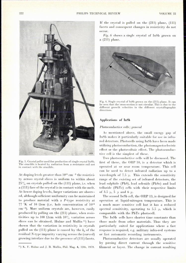
Single crystals are pulled by the Czochralskimethod 10), in which a rotating seed crystal isslowly withdrawn from a melt of the material.A typical crystal puller is shown in fig. 5. Crystalsare grown under vacuum at a rate of 2.5 cm/hourand a rotation rate of 120 rpm. It has been observedthat donor concentrations are markedly lower undervacuum than when pulling in a gaseous ambient.During pulling there is a relatively large loss ofantimony (about 0.1%), but the solubility of in-dium in indium antimonide is evidently sufficientlylow that the stoichiometry of the crystal is notappreciably affected. Undoped crystals, which areN-type, due to residual impurities, have an electronconcentration of approximately 1014 cm-3 and canhave mobilities up to 650000 cm2jVs at 77 OK
as mentioned earlier.Germanium is an acceptor in InSb and is used
for doping in preference to Zn and Cd, which arevolatile in vacuum. It has a ko of 0.02, givingan acceptor concentration varying by a factor of 2during the pulling of the first 50% of the melt.
8) J. B. Mullin, J. Electronics and Control 4, 358, 1958.9) T. C. Harrnan, J. Elcctrochem. Soc. 103, 128, 1956.10) J. Czochralski, Z. phys. Chem. 92, 219, 1917. See also
B. Okkerse, Philips tech. Rev. 21, 340, 1959/60 (No. 11).
222 PHILIPS TECHNICAL REVIEW VOLUME 22
Fig. 5. Crystal puller used for production of single crystal InSb.The crucible is heated by radiation from a resistance coil notin contact with the crucible.
At doping levels greater than 1015 cm+'' the resistivi-ty across crystal slices is uniform to within about25% on crystals pulled on the (111) plane, i.e. whena (Ill) face ofthe crystal is in contact with the melt.At lower doping levels, larger variations are observ-ed, although sufficient uniformity can be maintainedto produce material with a P-type resistivity at77 OK of 10 Dcm (i.e. hole concentration of 1014
cm-3). More uniform crystals are, however, easilyproduced by pulling on the (211) plane, when resis-tivities up to 100 Dcm with 10% variation acrossslices can be obtained. Hulme and Mullin 11) haveshown that the variation in resistivity in crystalspulled on the (111) plane is caused by the ko of theresidual N-type impurity varying across the (curved)growing interface due to the presence of (111) facets.
11) K. F. Hulme and ]. B. Mullin, Phil. Mag. 4, 1286, 1959.
If the crystal is pulled on the (211) plane, (111)facets and consequent changes in resistivity do notoccur.
Fig. 6 shows a single cryst al of InSb grown ona (211) plane.
Fig. 6. Single crystal of InSb grown on the (211) plane. It canbe seen that the cross-section is not circular. This is due to thedifferent growth velocities in the different crystallographicdirections.
Applications of InSh
Photoconductive cells; general
As mentioned above, the small energy gap ofInSb makes it particularly suitable for use in infra-red detectors. Photocells using InSb have been madeutilising photoconduction, the photomagnetoelectriceffect or the photovoltaic effect. The photoconduc-tive cell is the simplest of these.Two photoconductive cells will be discussed. The
first of these, the ORP 10, is a detector which isoperated at or near room temperature. This cellcan be used to detect infrared radiation up to awavelength of 7.5 fL. This extends the sensitivityrange of the existing set of infrared detectors, thelead sulphide (PbS), lead selenide (PbSe) and leadtelluride (PbTe) cells with their respective limitsof 3.5 fL, 5 fL and 6 [1-.
The second InSb cell, the ORP 13, is designed foroperation at liquid-nitrogen temperature. This isa much more sensitive cell but it has a reducedspectral sensitivity, operating to 5.5 fL, which iscomparable with the PbTe photocell.
The IrrSh cells have shorter time constants thanthose made from other materials. Thus they areparticularly suited for applications where a fastresponse is required, e.g. military infra-red systemsor fast automatic recording instruments.
Photoconductive detectors are usually operatedby passing direct current through the sensitivefilament or layer. The change in current resulting

1960/61, No. 7 PROPERTIES AND APPLICATIONS OF INDIUM ANTIMONIDE 223
from the increase in conductance during illuminationis then amplified and measured. In order to facili-tate amplification, the incident radiation is usuallychopped at a suitable frequency, often near 1 kcjs.When the performances of detectors at a given
wavelength and in a particular system are compared,there are two cell characteristics which are impor-tant. These determine the overall signal-to-noiseratio of the two cases, (a) system noise large com-pared with cell noise, and (b) system noise smallcompared with cell noise.For case (a) the performance is determined by the
responsivity, defined as the detector output voltageper unit incident signal power.In case (b) the noise equivalent power (N.E.P.)
is important. This is sometimes termed minimumdetectable energy. The N.E.P. is the incident radia-tion power for which the signal equals the cell noise.The N.E.P. is referred to a particular bandwidth,usually 1 cis.
The ORP 10 detector
This infra-red photocell is illustrated in fig. 7.It consists of a 10 fL thick strip of InSb attached to acopper mount drilled to facilitate mounting on aheat sink. The sensitive area is a rectangle 6 mm X
0.5 mm. The dark resistance of the cell is 100 Q,which is suitable for use with transistor amplifiers.
If, at room temperature, I photons per unit areaper second are incident on a filament of InSb ofwidth b and resistance R, the steady electric field inthe filament being E, then the open-circuit signalvoltage Vs is given by
Vs cc I e (/hn + /hp) rERb,
Fig. 7. The Mullard photoconductive cell ORP 10. The InSbelement is visible on the edge of the drilled copper block.The leads to the InSb run though the copper block whichthus serves as a heat sink during the soldering of connections.
where r is the lifetime of the charge carriers. If thclifetime in the material was independent of thecarrier concentration the signal could be increasedby increasing the resistivity, e.g. by doping thematerial with acceptors. However, it has been foundthat there is a decrease in lifetime which tends tooffset any increase in resistance obtained by doping.
Doping with acceptors increases the resistivity, which isgiven by the equation e = tneu, + pe/lp)-l when both elec-trons and holes part.icipate in the conduction process. Otherconditions which hold are np = n;2 and p - n = nA, where n;
is the intrinsic carrier concentration and nA the acceptorconcentration. With the aid of these relationships it can beshown that .Qmax occurs when
_ ,(!',,-/lp\nA - n, !_~I
I !'n /lp
and not for nA = 0, i.e. intrinsic material.
The noise is found to be always lcss than twicethe Johnson noise whose voltage is denoted Vn.'Now
v IV (/hn + /hp) rs n oe /
fa(5)
(4)
for a given power dissipation in the filament. Thisquantity decreases with increased doping: intrinsicor near intrinsic material is thcrefore used for thecell.In Table IJ I, the characteristics of this cell are
compared with those of other photoconductive cells.The ORP 10 detector possesses the following spe-
cial features:1) Rapid measurements can be made of radiationswith wavelengths up to 7.5 fL. In this wavelengthrange the cell therefore supplants thermal bolo-meter detectors, which are rather slow.2) The cell is particularly suitable for spectrometerapplications. The form of the InSb element - anarrow strip - and its mounting permit an arrayto be used and simultaneous observation of severalbands seems feasible. Observations for extendedperiods of time may be made without complicatedcooling arrangements. The wide wavelengthrange, which includes the main atmospheric ab-sorption bands, permits the study of fundamentalabsorption bands of many chemical groups withoutthe use of thermal bolometer detectors. The latterare not conveniently incorporated into automaticequipment.3) The cell is sensitive to the thermal radiationfrom bodies at relatively low temperatures, e.g.the radiation from 1 cm? of a black body at40 oe can be easily measured at a range of 40 cm.

224 PHILIPS TECHNICAL REVIEW VOLUME 22
Table ITI. Comparison between some photoconductive cells.
Cell Type Effective Spectral Peak Time Dark I Sensitivity, noise and figure of meritcategory No. sensitive range response constant resistance
I Noise equiv-area Radiation Sensitivity Figurealent power of meritper unit D*
bandwidth(mm") (I.L) (fL) (usec) (H:!) (10-9 W) (cmjfLW)
ITungstenlamp at 3mAjlumen 0.055 110002700 oK
PbS 61 SV 36 0.3 - 3.5 1.8 - 2.8 75 1000.4000
1IBlack body
1
radiation 180 fLVjfLW 5 120at 200°C
PhSe 161 RV I 6I1.0 - 5.0
I2.0 - 4.31 <1.0 115 - 100 1IMO~lOchrom- 15 fLVjfLW I <8.5
I>29
atic at 4 fL
1 1
Monochrom-I 0.3 fLVjfLW I <4.I
>43atic at 6 fL
InSb ORP 10 3 0.6 - 7.5 5.0 - 7.2 <1.0 0.1 Black bodyradiation 0.36 fLVjfLW <10 >17
Iat 200°C
I I
Monochrom- \ 14 mVjfLW \ <0.02 >9000InSh atic at 4 fL
1
liquid- ORP 13 3.5 0.6 - 5.5 4.5 - 5.0 <10 20 - 40 Black bodynitrogen Icooled
I I
radiation 2.4 mVjfLW <0.12 >1500at 200°C
D* = (NEP)-Ix (area) t and is a figure of merit for photocells when used for detecting low-level radiation 12). D*, unlike NEP,is independent of photocell sensitive area and represents a sound basis for comparison of photocells of different area.
The ORP 13 cooled photoconducting cell
Detectors with the same light-sensitive area asthe ORPIO have been developed for operation atliquid nitrogen temperature, see figs. 8 and 9.
Fig. 8. The Mullard cooled InSh cell ORP 13, in its metalhousing.
12) R. C. ]ones, Proc. Inst. Radio Engrs. 47, 14-95, 1959.
s_
4\13
6
2
5
4
Fig. 9. Construction of the cooled InSb cell. The InSh element1 is cooled by filling the Dewar flask 2 with liquid nitrogen.A demountable mirror 3 facilitates the measurement of hori-zontally incident radiation. A sapphire window 4 is sealed tothe Dewar flask just in front of the InSb strip. The Dewar ishoused in a metal tube 5 containing a resilient filling 6. Theleads 7 of the cell pass through glass-metal seals in theDewar flask.
The values of the parameters in equation (4)are modified at this temperature. P-type material isused because the hole mobility is much less thanthe electron mobility - this gives high resistivity,
1960/61, No. 7 PROPE;RTIES AND APPLICATIONS OF INDIUM ANTIMONIDE 225
about 30 times the room temperature value, andtherefore high cell resistance and large signals. Theprocess determining the lifetime of excess holes andelectrons is electron trapping. The signal voltage Vsis given by
Vs oe I e !-lp Op RE b ,
where Op is the hole lifetime.
At this temperature the resistivity would be decreased bydoping because there are a negligible number of intrinsiccarriers present. The product Jtp -Cp would also be decreased bydoping. The purest possible P-type material is therefore used.
In this cell the noise appears to be semiconductor"fluctuation noise" (fluctuations in the recombina-tion process). Using P-type material of resistivityat 77 "K of up to 10 Dcm the characteristics givenin Table III are obtained.
After the cell has been exposed to visible radiationwhile cooled, a quasi-permanent change in the darkresistance takes place. The original resistance valuemay be re-attained by allowing the cell to warmto room temperature and then cooling it once more.
Owing to its great sensitivity this cooled detectoris a useful addition to the present range of photo-conductive cells.
Hall generators
Indium antimonide has been quite widely used asthe basis of Hall generators. These are devices inwhich the output signal is proportional to the prod-uct of two currents, either of which may be steadyor variable. One of the currents is passed througha plate of the material (as in the measurement ofthe Hall effect, see page 219) and the other is fedinto the winding of an electromagnet producing the
(6)
magnetic field on the plate. The output voltagefrom the Hall probes is then proportional to theproduct of the two currents. A load may be insertedbetween the Hall probes and power drawn in theoutput circuit.Many applications and refinements of these de-
vices have been described in the literature. Consid-erations concerning this type of device will formthe subject of a forthcoming article in this journal.
The large magnetoresistance effect in InSb haslikewise led to a number of applications, includingdisplacement gauges and tiny measuring probes forhigh intensity magnetic fields. In these devices adisc geometry is often used for the InSb element;this arrangement gives a large change in resistancewhen a magnetic field is applied. The magnetoresis-tance effect is proportional to the square of the car-rier mobility, thus InSb is particularly suitable forsuch applications.
Summary. Indium antimonide is a compound with semico n-ducting properties. The small energy gap makes it a goodphotoconductor. This has led to the construction of photo-conductive cells with either long-wavelength response (theMullard ORP 10 to 7.5 (.L) or high sensitivity (the MullardORP 13, cooled with liquid nitrogen, with a sensitivity of 14mV/(.LWat4 (.L). Moreover the lifetime ofthe free charge carriersis very short, so that InSb cells are very fast: the time constantof the ORP 10 is <1 (.Lsec,that of the ORP 13 is <10 (.Lsec.The electron mobility is observed to be very high (650 000
cm2/Vs at 77 OK), making InSb also particularly suited foruse in Hall generators. The large magnetoresistance effect inInSb has likewise led to a number of applications, includingdisplacement gauges and tiny measuring probes for high in-tensity magnetic fields.Very pure single crystals of InSb are prepared from pre-
viously purified indium and antimony. The compound isfurther purified by zone melting, after which single crystals areformed by pulling from the melt on the (211) plane. Dopingwith Ge (for example) gives P-type material, while withoutdoping it is N-type because of residual impurities.