pci express 3.0 and 4.0 test tim fairfield fae challenges: tim … · 2015-04-22 · pci express...
TRANSCRIPT

PCI Express 3.0 and 4.0 Test Challenges: Link Equalization Testing 8Gbps vs 16Gbps Rx Testing
Tim Fairfield
FAE
Mark Roberts
FAE
Revised
April 8, 2015

Page
Agenda
– PCI-SIG Spec Development: Gen3/Gen4
– What is Dynamic Link Equalization
– PCI Express PHY Test Requirements (Link EQ)
– Rx Jitter Calibration
– Live Demo of PCIE Link EQ Test
– PCIE Gen4 Test Challenges
– Summary
PCIe 3/4 Test
Challenges 2

Page
22-Apr-15
Sequential Development of PCIe Specs and Scope
Base Specification
• Contains all the
system knowledge
• Can directly be
applied to Chip
Test:
Card Electromechanical (CEM) Spec
• Applies to Add-In Cards and
Mother Boards
• Mitigates card manufacturer’s
need to study the base
specification
• Increases reproducibility through
PCI-SIG supplied test tools CBB
and CLB (compliance base and
load board)
Phy Test Specification
• Defines compliance
tests of CEM spec in
detail
PCIe 3/4 Test
Challenges
3

Page
22-Apr-15
4
Gen4 Features and Specifications
Revision 4.0 3.0 2.0 1.1
Signal
Speed
16Gbps
8Gbps
5Gbps
2.5Gbps
8Gbps
5Gbps
2.5Gbps 5Gbps
2.5Gbps 2.5Gbps
Encoding 16G, 8G: 128b/130b
<8G: 8b/10b
8G: 128b/130b
<8G: 8b/10b 8b/10b 8b/10b
Equalization
16G,8G:
Tx: Pre1, Post1
Rx: CTLE+DFE
<8G: Tx Post 1
5G: -3.5/ -6dB
2.5G: -3.5dB
8G:
Tx: Pre1, Post1
Rx: CTLE+DFE
<8G: Tx Post 1
5G: -3.5/ -6dB
2.5G: -3.5dB
Tx: Post 1
5G: -3.5/ -
6dB
2.5G: -
3.5dB
Tx: Post 1
-3.5dB
PCIe 4.0 Adds 16GB/s Support

Page
22-Apr-15
PCIe 4.0 Outlook and Test Challenges
• New data rate will be added 16GT/s
• Requires an output stages capable of providing pre-shoot and de-emphasis with fast enough rise-times.
• Link Equalization protocol will be similar to Gen 3
• TxEQ P0-P10
• RxEQ CTLE + 2tap DFE
• Max Channel Length (shorter) – more needs for Re-timers and Re-drivers
• RX clocking architectures: CC, DC and IR
• CC Common RefClock synchronous RX and TX
• DC Data Clocked synchronous or asynchronous RX and TX
• IR Independent RefClock asynchronous RX and TX
• SKP OS filtering is required!
• RX testing procedure will be standardized for all data rates 2.5GT/s, 5GT/s, 8GT/s and 16GT/s
PCIe 3/4 Test
Challenges
5

Page
Agenda
– PCI-SIG Spec Development: Gen3/Gen4
– What is Dynamic Link Equalization
– PCI Express PHY Test Requirements (Link EQ)
– Rx Jitter Calibration
– Live Demo of PCIE Link EQ Test
– PCIE Gen4 Test Challenges
– Summary
PCIe 3/4 Test
Challenges 6

Page
22-Apr-15
What do we mean by a “Dynamic Channel” ?
PCIe 3/4 Test
Challenges
7

Page
22-Apr-15
8
Why Test Receivers?
2.5Gbps
5Gbps
8Gbps
16 Gbps
TX
RX

Page
22-Apr-15
Tx/Rx Link for PCIe 3.0
PCIe 3/4 Test
Challenges
9
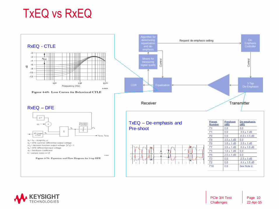
Block Diagram of Transmitter and Receiver Architecture
3-Tap
De-Emphasis Equalization CDR
Receiver Transmitter
Means for
measuring
signal quality
Algorithm for
determining
equalization
and de-
emphasis
De-
Emphasis
Controller
Request de-emphasis setting
Contr
ol
Contr
ol
Page
22-Apr-15
TxEQ vs RxEQ
PCIe 3/4 Test
Challenges
10
u
RxEQ - CTLE
RxEQ – DFE
TxEQ – De-emphasis and
Pre-shoot

Page
22-Apr-15
Dynamic Equalization
PCIe 3/4 Test
Challenges
11
Root Complex and End Point will negotiate the optimized EQ Setting

Page
22-Apr-15
Dynamic Link Equalization Handshake
PCIe 3/4 Test
Challenges
12
The four phases of the Link Equalization Protocol
Recovery.RcvrCfg
Recovery.Equalization
Add-in Card System Board
System Board tells the Add-in Card
which initial preset to use after the
speed change will have been done.
Link partners settle on 8GT/s speed.
Exchange FS/LF values.
Add-in Card sets up the de-
emphasis of the System Board’s
transmitter.
System Board sets up the de-
emphasis of the Add-in Card’s
transmitter.

Page
22-Apr-15
Dynamic Link Equalization Loopback
PCIe 3/4 Test
Challenges
13
The Link Training Status State Machine

Page
Agenda
– PCI-SIG Spec Development: Gen3/Gen4
– What is Dynamic Link Equalization
– PCI Express PHY Test Requirements (Link EQ)
– Rx Jitter Calibration
– Live Demo of PCIE Link EQ Test
– PCIE Gen4 Test Challenges
– Summary
PCIe 3/4 Test
Challenges 14

Page
22-Apr-15
Tx/Rx Link Equalization Testing for PCIe 3.0
PCIe 3/4 Test
Challenges
15
According to PCI Express Electrical PHY Test Specification
Test Number Test Name
2.3 Add-in Card Transmitter Initial Tx EQ Test for
8.0GT/s
2.4 Add-in Card Transmitter Link Equalization Response
Test for 8GT/s
2.7 System Board Transmitter Link Equalization
Response Test for 8GT/s
2.10 Add-in Card Receiver Link Equalization Test for
8GT/s
2.11 System Board Receiver Link Equalization Test for
8GT/s

Page
22-Apr-15
Tx/Rx Link Equalization Testing for PCIe 3.0
PCIe 3/4 Test
Challenges
16
Tests 2.3, 2.4, and 2.7 focus on the transmitter
3-Tap
De-Emphasis Equalization CDR
Receiver Transmitter
Means for
measuring
signal quality
Algorithm for
determining
equalization
and de-
emphasis
De-
Emphasis
Controller
Request de-emphasis setting
Contr
ol
Contr
ol
The PCIe 3.0 Receiver Link Equalization
Tests specified in 2.3 and 2.4 and 2.7
provide insight to TxEQ issues and corner
case situations
• Requires the DUT to negotiate using
both Presets and Cursors values
• Determines if DUT responds to
Preset/Cursor requests in the
specified amount of time
• Troubleshoot the issues between
protocol communication vs PHY layer
performance

Page
22-Apr-15
Tx/Rx Link Equalization Testing for PCIe 3.0
PCIe 3/4 Test
Challenges
17
Tests 2.10 and 2.11 focus on the receiver
3-Tap
De-Emphasis Equalization CDR
Receiver Transmitter
Means for
measuring
signal quality
Algorithm for
determining
equalization
and de-
emphasis
De-
Emphasis
Controller
Request de-emphasis setting
Contr
ol
Contr
ol
The PCIe 3.0 Receiver Link Equalization Tests
specified in 2.10 and 2.11 are the most
important test of a DUT, they:
• Determine the DUT’s ability to request
appropriate amounts of transmitter
equalization
• Determine the DUT’s ability to
internally apply the appropriate amount
of receiver equalization
• Determine the quality of the DUT’s
algorithm for optimizing the link quality
• Determine the DUT’s ability to optimize
TxEQ and RxEQ in a short period of
time

Page
Agenda
– PCI-SIG Spec Development: Gen3/Gen4
– What is Dynamic Link Equalization
– PCI Express PHY Test Requirements (Link EQ)
– Rx Jitter Calibration
– Live Demo of PCIE Link EQ Test
– PCIE Gen4 Test Challenges
– Summary
PCIe 3/4 Test
Challenges 18

Page
22-Apr-15
CEM Rx Jitter Tolerance Spec
PCIe 3/4 Test
Challenges
19
According to PCI Express Electrical PHY Test Specification
Parameter Min Max Unit SigTest
Technology Template
Vpp 800 mV N/A N/A
RJ (Random Jitter) 1.5 1.7 ps RMS PCI_3_0_RX_CAL PCIE_3_8GB_Rx_Sj_CAL
SJ (Sinusoidal Jitter)
@ 100 MHz
12.5 13.5 ps PP PCI_3_0_RX_CAL PCIE_3_8GB_Rx_Sj_CAL
Differential Mode
Sinusoidal
Interference at 2.1 GHz
14 16 mV PP N/A N/A
VRX-EH-8G Eye Height AIC:
41 to 46
System:
45 to 50
mV PCI_3_0_RX_CAL AIC: PCIE_3_8GB_RX
CARD_CAL_MULTI_CTLE_DFE_EMBED01
System: PCIE_3_8GB_RX
SYS_CAL_MULTI_CTLE_DFE_
EMBED01
TRX-EW-8G Eye Width AIC:
39.25 to
41.25
System:
43 to 45
ps PCI_3_0_RX_CAL AIC: PCIE_3_8GB_RX
CARD_CAL_MULTI_CTLE_DFE_EMBED01
System: PCIE_3_8GB_RX
SYS_CAL_MULTI_CTLE_DFE_
EMBED01

Page
22-Apr-15
20
Calibrating Stressed Eye: PCIe 3.0 @8 GB/s
20
8 GT/s PRBS Generator
Combiner Test EquipmentCalibration ChannelReplica Channel
Fixed TX EQ
TP1 TP2
Post Processing Scripts:Rx pkg modelBehaviorial CTLE/DFEBehavioral CDR
TP2P
Rj Source
Sj Source
Diff Interfer
ence
CM Interfer
ence
EW Adjust EH Adjust
25 mV / .3 UI at E-12 BER

Page
22-Apr-15
21
Techniques For Calibrating Stressed Eye: 16GT/s
16 GT/s PRBS Generator
Combiner Test EquipmentReplica Channel
CEM Connector
Fixed TX EQ
TP1 TP2
Post Processing Scripts:Rx pkg modelBehaviorial CTLE/DFEBehavioral CDR
TP2P
Rj Source
Sj Source
Diff Interfer
ence
CM Interfer
ence
Calibration ChannelEH or EW Adjust
Small EW Adjust
Small EH Adjust
25 mV / .3 UI at E-12 BER

Page
22-Apr-15
Setup
PCIe 3/4 Test
Challenges
22
Build in Jitter Sources:
- 8 Tap De-emphasis
- SJ
- RJ
- DMI
- CMI (Base Spec)
- Clock Multiplier
- ISI Channel Emulation
- Error Detector Equalization

Page
22-Apr-15
RX Calibration from MOI
PCIe 3/4 Test
Challenges
23
Keysight - PCIe Gen 3.0 CEM RX Test MOI – SIG (excerpt)

Page
22-Apr-15
Calibration Can be done Manually
PCIe 3/4 Test
Challenges
24
MOI is 92 Pages can take up to 8 hours!

Page
22-Apr-15
or…
PCIe 3/4 Test
Challenges
25
Page
22-Apr-15
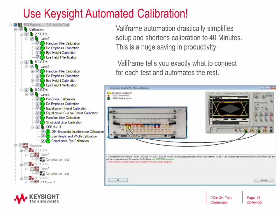
Use Keysight Automated Calibration!
PCIe 3/4 Test
Challenges
26
Valiframe automation drastically simplifies
setup and shortens calibration to 40 Minutes.
This is a huge saving in productivity
Valiframe tells you exactly what to connect
for each test and automates the rest.

Page
22-Apr-15
Presets and Amplitude
PCIe 3/4 Test
Challenges
27
Automated by ValiFrame Software

Page
22-Apr-15
SJ and RJ
PCIe 3/4 Test
Challenges
28
Automated by ValiFrame Software
0
0.75
1.5
2.25
3
3.75
4.5
5.25
6
6.75
7.5
0 1 2 3 4 5
Measure
d R
andom
Jitt
er
[ps]
Set Random Jitter [ps]
L0_Cal_8GTps_RJ
for PCI Express 3.0 Add-In Card
MeasuredRandom Jitter
0
7.5
15
22.5
30
37.5
45
52.5
60
67.5
75
0 10 20 30 40 50
Measure
d S
J [ps]
Set SJ [ps]
L0_Cal_8GTps_SJ
for PCI Express 3.0 Add-In Card
SJ (5 MHz)
SJ (100 MHz)

Page
22-Apr-15
DMI and Eye
PCIe 3/4 Test
Challenges
29
04080
120160200240280320360400
0 80 160 240 320 400
Measure
d D
M I
nte
rfere
nce [
mV
]
Set DM Interference [mV]
L0_Cal_8GTps_CBB3_DM_SI for PCI Express 3.0 Add-In Card
Measured DMSI Amplitude
07.515
22.530
37.545
52.560
67.575
15 19 23 27 31 35
Measure
Eye W
idth
[ps]
DM Interference [mV]
L0_Cal_8GTps_CBB3_Eye_Width
for PCI Express 3.0 Add-In Card
Eye Width(0.5ps RJ)
Eye Width(2.5ps RJ)
0
7.5
15
22.5
30
37.5
45
52.5
60
67.5
75
15 19 23 27 31 35
Measure
d E
ye H
eig
ht
[mV
]
DM Interference [mV]
L0_Cal_8GTps_CBB3_Eye_Height for PCI Express 3.0 Add-In Card
Eye Height(0.5ps RJ)
Eye Height(2.5ps RJ)

Page
22-Apr-15
Set up BERT to generate compliance pattern with P7 activated:
1. Adjust DM-SI to meet specified EH
2. Adjust RJ to meet specified EW
3. Re-check EH and if necessary re-adjust DM-SI once
4. Record the final calibration values RJcal and DM-SIcal for later usage
Final Calibrated Eye
PCIe 3/4 Test
Challenges
30

Page
22-Apr-15
Quick Demo of Automated Calibration
– "C:\Program Files (x86)\BitifEye\ValiFrame\PCI-Express3"
PCIe 3/4 Test
Challenges
31

Page
Agenda
– PCI-SIG Spec Development: Gen3/Gen4
– What is Dynamic Link Equalization
– PCI Express PHY Test Requirements (Link EQ)
– Rx Jitter Calibration
– Live Demo of PCIE Link EQ Test
– PCIE Gen4 Test Challenges
– Summary
PCIe 3/4 Test
Challenges 32

Page
22-Apr-15
Tx/Rx Link Equalization Testing for PCIe 3.0
PCIe 3/4 Test
Challenges
33
According to PCI Express Electrical PHY Test Specification
Test Number Test Name
2.3 Add-in Card Transmitter Initial Tx EQ Test for
8.0GT/s
2.4 Add-in Card Transmitter Link Equalization Response
Test for 8GT/s
2.7 System Board Transmitter Link Equalization
Response Test for 8GT/s
2.10 Add-in Card Receiver Link Equalization Test for
8GT/s
2.11 System Board Receiver Link Equalization Test for
8GT/s

Page
22-Apr-15
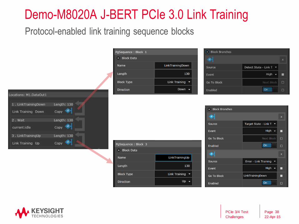
Live Demo of Add in Card Link EQ Test
M8020 J-Bert
LTSSM Capture
Link Training
Logic Enabled Sequencer
Protocol-enabled link training sequence blocks
PCIe 3/4 Test
Challenges
34

Page
22-Apr-15
Demo-M8020A J-BERT LTSSM Capture
PCIe 3/4 Test
Challenges
35
Link training logging: LTSSM state transitions

Page
22-Apr-15
Demo-PCIe 3.0 Receiver Link Equalization Testing
PCIe 3/4 Test
Challenges
36
Example of AIC tests
– Measurements made with M8020A J-
BERT and PCI-SIG interface boards
• Full calibrations were performed
• Integrated de-emphasis and
sinusoidal interference give us a
very clean lab bench (ignore all
the mess in the background, it’s
not necessary for the test!)

Page
22-Apr-15
Demo-M8020A J-BERT PCIe 3.0 Link Training
PCIe 3/4 Test
Challenges
37
Logic-enabled sequencer
Page
22-Apr-15
Demo-M8020A J-BERT PCIe 3.0 Link Training
PCIe 3/4 Test
Challenges
38
Protocol-enabled link training sequence blocks

Page
22-Apr-15
Demo-M8020A J-BERT PCIe 3.0 Link Training
PCIe 3/4 Test
Challenges
39
Link training logging: Link Equalization settings

Page
22-Apr-15
Demo-Different DUT LTSSM Examples
PCIe 3/4 Test
Challenges
40
Link training logging: Link Equalization settings
Accept PresetNumber PreCursor DataCursor PostCursor
True P7 - - -
True - 0 24 0
True - 0 23 1
True - 0 22 2
True - 0 21 3
True - 0 20 4
True - 0 19 5
True - 0 18 6
True - 0 17 7
True - 0 16 8
True - 1 23 0
True - 1 22 1
True - 1 21 2
True - 1 20 3
True - 1 19 4
True - 1 18 5
True - 1 17 6
True - 1 16 7
True - 2 22 0
True - 2 21 1
True - 2 20 2
True - 2 19 3
True - 2 18 4
True - 2 17 5
True - 2 16 6

Page
22-Apr-15
Demo-Different DUT LTSSM Examples
PCIe 3/4 Test
Challenges
41
Link training logging: Link Equalization settings
Accept PresetNumber PreCursor DataCursor PostCursor
True - 3 21 0
True - 3 20 1
True - 3 19 2
True - 3 18 3
True - 3 17 4
True - 3 16 5
True - 4 20 0
True - 4 19 1
True - 4 18 2
True - 4 17 3
True - 4 16 4
True - 5 19 0
True - 5 18 1
True - 5 17 2
True - 5 16 3
True - 6 18 0
True - 6 17 1
True - 6 16 2
True - 4 17 3

Page
22-Apr-15
END of Live Demo
PCIe 3/4 Test
Challenges
42
Next –wrap up

Page
Agenda
– PCI-SIG Spec Development: Gen3/Gen4
– What is Dynamic Link Equalization
– PCI Express PHY Test Requirements (Link EQ)
– Rx Jitter Calibration
– Live Demo of PCIE Link EQ Test
– PCIE Gen4 Test Challenges
– Summary
PCIe 3/4 Test
Challenges 43

Page
22-Apr-15
Integration at 16Gbps
PCIe 3/4 Test
Challenges
44
>16Gbps BERT
Jitter and De-emphasis
Link Equalization

Page
22-Apr-15
New Test Challenges:
PCIe 3/4 Test
Challenges
45
Error Detector equalization
(CTLE 16G) to overcome long
DUT channels
ISI Channel Emulation

Page
Agenda
– PCI-SIG Spec Development: Gen3/Gen4
– What is Dynamic Link Equalization
– PCI Express PHY Test Requirements (Link EQ)
– Rx Jitter Calibration
– Live Demo of PCIE Link EQ Test
– PCIE Gen4 Test Challenges
– Summary
PCIe 3/4 Test
Challenges 46

Page
22-Apr-15
Summary: PCIe 3.0 Receiver Link Equalization Testing
PCIe 3/4 Test
Challenges
The M8020A J-BERT delivers insight to your DUT’s behavior
– Link Equalization Testing is critical to ensure device interoperability
• Dynamic Equalization is necessary for different combinations of upstream and downstream devices
• PCI-SIG requires Link Equalization Testing for certification
– The M8020A J-BERT delivers insight to your DUT’s behavior
• Time-stamped LTSSM state transition logs allow analysis of state machine transition and identification of problems
- Example: I didn’t know my DUT was spending so much time in Recovery.RcvrCfg!
• Link Equalization request logs allow analysis of DUT algorithm
- Example: I didn’t know my DUT was only asking for preshoot!
• Link Equalization settings allow deeper characterization
- Example: I had no idea my DUT result changes so much based on suggested starting Preset!
47

Page
22-Apr-15
PCIe 3/4 Test
Challenges
48
Thank you!