on teaching fast adder designs: revisiting ladner & fischerguy/papers/ppc_adder_tutorial.pdf ·...
TRANSCRIPT
On teaching fast adder designs: revisiting Ladner & Fischer∗
Guy Even †
February 1, 2006
Abstract
We present a self-contained and detailed description of the parallel-prefix adder of Ladnerand Fischer. Very little background is assumed in digital hardware design. The goal is tounderstand the rational behind the design of this adder and view the parallel-prefix adderas an outcome of a general method.
∗This essay is from the book: Shimon Even Festschrift, edited by Goldreich, Rosenberg, and Selman, LNCS
3895, pp. 313-347,2006 . c©Springer-Verlag Belin Heidelberg 2006.†Department of Electrical-Engineering, Tel-Aviv University, Israel. E-mail:[email protected]
CONTENTS 1
Contents
1 Introduction 21.1 On teaching hardware . . . . . . . . . . . . . . . . . . . . . . . . . . . . . . . . . 21.2 A brief summary . . . . . . . . . . . . . . . . . . . . . . . . . . . . . . . . . . . . 31.3 Confusing terminology (a note for experts) . . . . . . . . . . . . . . . . . . . . . 31.4 Questions . . . . . . . . . . . . . . . . . . . . . . . . . . . . . . . . . . . . . . . . 41.5 Organization . . . . . . . . . . . . . . . . . . . . . . . . . . . . . . . . . . . . . . 4
2 Preliminaries 42.1 Digital operation . . . . . . . . . . . . . . . . . . . . . . . . . . . . . . . . . . . . 42.2 Building blocks . . . . . . . . . . . . . . . . . . . . . . . . . . . . . . . . . . . . . 52.3 Combinational circuits . . . . . . . . . . . . . . . . . . . . . . . . . . . . . . . . . 62.4 Synchronous circuits . . . . . . . . . . . . . . . . . . . . . . . . . . . . . . . . . . 82.5 Finite state machines . . . . . . . . . . . . . . . . . . . . . . . . . . . . . . . . . . 92.6 Cost and Delay . . . . . . . . . . . . . . . . . . . . . . . . . . . . . . . . . . . . . 92.7 Notation . . . . . . . . . . . . . . . . . . . . . . . . . . . . . . . . . . . . . . . . . 102.8 Representation of numbers . . . . . . . . . . . . . . . . . . . . . . . . . . . . . . . 11
3 Definition of a binary adder 113.1 Importance of specification . . . . . . . . . . . . . . . . . . . . . . . . . . . . . . 113.2 Combinational adder . . . . . . . . . . . . . . . . . . . . . . . . . . . . . . . . . . 123.3 Bit-serial adder . . . . . . . . . . . . . . . . . . . . . . . . . . . . . . . . . . . . . 13
4 Trivial designs 134.1 A bit-serial adder . . . . . . . . . . . . . . . . . . . . . . . . . . . . . . . . . . . . 134.2 Ripple-carry adder . . . . . . . . . . . . . . . . . . . . . . . . . . . . . . . . . . . 144.3 Cost and Delay . . . . . . . . . . . . . . . . . . . . . . . . . . . . . . . . . . . . . 17
5 Lower bounds 17
6 The adder of Ladner and Fischer 186.1 Motivation . . . . . . . . . . . . . . . . . . . . . . . . . . . . . . . . . . . . . . . 186.2 Associativity of composition . . . . . . . . . . . . . . . . . . . . . . . . . . . . . . 206.3 The parallel prefix problem . . . . . . . . . . . . . . . . . . . . . . . . . . . . . . 226.4 The parallel prefix circuit . . . . . . . . . . . . . . . . . . . . . . . . . . . . . . . 226.5 Correctness . . . . . . . . . . . . . . . . . . . . . . . . . . . . . . . . . . . . . . . 246.6 Delay and cost analysis . . . . . . . . . . . . . . . . . . . . . . . . . . . . . . . . 246.7 The parallel-prefix adder . . . . . . . . . . . . . . . . . . . . . . . . . . . . . . . . 25
7 Further topics 267.1 The carry-in bit . . . . . . . . . . . . . . . . . . . . . . . . . . . . . . . . . . . . . 267.2 Compound adder . . . . . . . . . . . . . . . . . . . . . . . . . . . . . . . . . . . . 277.3 Fanout . . . . . . . . . . . . . . . . . . . . . . . . . . . . . . . . . . . . . . . . . . 277.4 Tradeoffs between cost and delay . . . . . . . . . . . . . . . . . . . . . . . . . . . 287.5 VLSI area . . . . . . . . . . . . . . . . . . . . . . . . . . . . . . . . . . . . . . . . 28
8 An opinionated history of adder designs 29
1 INTRODUCTION 2
9 Discussion 30
1 Introduction
This essay is about how to teach adder designs for undergraduate Computer Science (CS) andElectrical Engineering (EE) students. For the past eight years I have been teaching the secondhardware course in Tel-Aviv University’s EE school. Although the goal is to teach how to builda simple computer from basic gates, the part I enjoy teaching the most is about addition. Atfirst I thought I felt so comfortable with teaching about adders because it is a well defined, verybasic question, and the solutions are elegant and can be proved rigorously without exhaustingthe students. After a few years, I was able to summarize all these nice properties simply bysaying that this is the most algorithmic topic in my course. Teaching has helped me realize thatappreciation of algorithms is not straightforward; I was lucky to have been influenced by myfather. In fact, while writing this essay, I constantly asked myself how he would have presentedthis topic.When writing this essay I had three types of readers in mind.
• Lecturers of undergraduate CS hardware courses. Typically, CS students have a goodbackground in discrete math, data structures, algorithms, and finite automata. However,CS students often lack enthusiasm for hardware, and the only concrete machine theyare comfortable with is a Turing machine. To make teaching easier, I added a ratherlong preliminaries section that defines the hardware model and presents some hardwareterminology. Even combinational gates and flip-flops are briefly described.
• Lecturers of undergraduate EE hardware students. In contrast to CS students, EE stu-dents are often enthusiastic about hardware (including devices, components, and commer-cial products), but are usually indifferent to formal specification, proofs, and asymptoticbounds. These students are eager to learn about the latest buzzwords in VLSI and mi-croprocessors. My challenge, when I teach about adders, is to convince the students thatlearning about an old and solved topic is useful.
• General curious readers (especially students). Course material is often presented in theshortest possible way that is still clear enough to follow. I am not aware of a text thattells a story that sacrifices conciseness for insight about hardware design. I hope thatthis essay could provide such insight to students interested in learning more about whathappens “behind the screen”.
1.1 On teaching hardware
Most hardware textbooks avoid abstractions, definitions, and formal claims and proofs (Mullerand Paul [MullerPaul00] is an exception). Since I regard hardware design as a subbranch ofalgorithms, I think it is a disadvantage not to follow the format of algorithm books. I tried tofollow this rule when I prepared lecture notes for my course [Even04]. However, in this essay Iam lax in following this rule. First, I assumed that the readers could easily fill in the missingformalities. Second, my impression of my father’s teaching was that he preferred clarity overformality. On the other hand, I tried to present the development of a fast adder in a systematicfashion and avoid ad-hoc solutions. In particular, a distinction is made between concepts and

1 INTRODUCTION 3
representation (e.g., we interpret the celebrated “generate-carry” and “propagate-carry” bits asa representation of functions, and introduce them rather late in a specific design in Sec. 6.7).
I believe the communication skills of most computer engineers would greatly benefit if theyacquired a richer language. Perhaps one should start by modeling circuits by graphs andusing graph terminology (e.g., out-degree vs. fanout, depth vs. delay). I decided to stickto hardware terminology since I suspect that people with a background in graphs are moreflexible. Nevertheless, whenever possible, I tried to use graphs to model circuits (e.g., netlists,communication graphs).
1.2 A brief summary
This essay mainly deals with the presentation of one of the parallel-prefix adders of Ladner andFischer [LadnerFischer80]. This adder was popularized by Brent and Kung [BrentKung82] whopresented a regular layout for it as well as a reduction of its fanout. In fact, it is often referredto as the “Brent-Kung” adder. Our focus is on a detailed and self-contained explanation of thisadder.
The presentation of the parallel-prefix adder in many texts is short but lacks intuition(see [BrentKung82, MullerPaul00, ErceLang04]). For example, the carry-generate (gi) andcarry-propagate (pi) signals are introduced as a way to compute the carry bits without explainingtheir origin1. In addition, an associative operator is defined over pairs (gi, pi) as a way to reducethe task of computing the carry-bits to a prefix problem. However, this operator is introducedwithout explaining how it is derived.
Ladner and Fischer’s presentation does not suffer from these drawbacks. The parallel-prefixadder is systematically obtained by “parallelizing” the “bit-serial adder” (i.e., the trivial finitestate machine with two states, see Sec. 4.1). According to this explanation the pair of carry-generate and carry-propagate signals represent three functions defined over the two states ofthe bit-serial adder. The associative operator is simply a composition of these functions. Themystery is unravelled and one can see the role of each part.
Ladner and Fischer’s explanation is not long or complicated, yet it does not appear intextbooks. Perhaps a detailed and self-contained presentation of the parallel-prefix adder willinfluence the way parallel-prefix adders are taught. I believe that students can gain much moreby understanding the rational behind such an important design. Topics taught so that thestudents can add some items to their “bag of tricks” often end up in the “bag of obscure andforgotten tricks”. I believe that the parallel-prefix adder belongs to the collection of fundamentalalgorithmic paradigms and can be presented as such.
1.3 Confusing terminology (a note for experts)
The terms “parallel-prefix adder” and “carry-lookahead adders” are used inconsistently in theliterature. Our usage of these terms refers to the algorithmic method employed in obtainingthe design rather than the specifics of each adder. We use the term “parallel-prefix adder” torefer to an adder that is based on a reduction of the task of computing the carry-bits to a prefixproblem (defined in Sec. 6.3). In particular, parallel-prefix adders in this essay are based on theparallel prefix circuits of Ladner and Fischer. The term “carry-lookahead adder” refers to anadder in which special gates (called carry-lookahead gates) are organized in a tree-like structure.
1The signals gi and pi are defined in Sec. 6.7
2 PRELIMINARIES 4
The topology is not precisely a tree for two reasons. First, often connections are made betweennodes in the same layer. Second, information flows both up and down the tree
One can argue justifiably that, according to this definition, a carry-lookahead is a specialcase of a parallel-prefix adder. To help the readers, we prefer to make the distinction betweenthe two types of adders.
1.4 Questions
Questions for the students appear in the text. The purpose of these questions is to help studentscheck their understanding, consider alternatives to the text, or just think about related issuesthat we do not focus on. Before presenting a topic, I usually try to convince the students thatthey have something to learn. The next question is a good example for such an attempt.
Question 1.1 1. What is the definition of an adder? (Note that this is a question abouthardware design, not about Zoology.)
2. Can you prove the correctness of the addition algorithm taught in elementary school?
3. (Assuming students are familiar with the definition of the delay (i.e., depth) of a com-binational circuit) What is the smallest possible delay of an adder? Do you know of anadder that achieves this delay?
4. Suppose you are given the task of adding very long numbers. Could you share this workwith friends so that you could work on it simultaneously to speed up the computation?
1.5 Organization
We begin with a preliminaries in Section 2. This section is a brief review of digital hardwaredesign. In Section 3, we define two types of binary adders: a combinational adder and a bit-serial adder. In Section 4, we present trivial designs for each type of adder. The synchronousadder is an implementation of a finite state machine with two states. The combinational adderis a “ripple-carry adder”. In Section 5, we prove lower bounds on the cost and delay of acombinational adder. Section 6 is the heart of the essay. In it, we present the parallel-prefixcircuit of Ladner and Fischer as well as the parallel-prefix adder. In Section 7, we discuss variousissues related to adders and their implementation. In Section 8, we briefly outline the historyof adder designs. We close with a discussion that attempts to speculate why the insightfulexplanation in [LadnerFischer80] has not made it into textbooks.
2 Preliminaries
2.1 Digital operation
We assume that inputs and outputs of devices are always either zero or one. This assumptionis unrealistic due to the fact that the digital value is obtained by rounding an analog value thatchanges continuously (e.g., voltage). There is a gap between analog values that are rounded tozero and analog values that are rounded to one. When the analog value is in this gap, its digitalvalue is neither zero or one.
The advantage of this assumption is that it simplifies the task of designing digital hardware.We do need to take precautions to make sure that this unrealistic assumption will not render
2 PRELIMINARIES 5
our designs useless. We set strict design rules for designing circuits to guarantee well definedfunctionality.
We often use the term signal. A signal is simply zero or one value that is output by a gate,input to a gate, or delivered by a wire.
2.2 Building blocks
The first issue we need to address is: what are our building blocks? The building blocks arecombinational gates, flip-flops, and wires. We briefly describe these objects.
Combinational gates. A combinational gate (or gate, in short) is a device that implementsa Boolean function. What does this mean? Consider a Boolean function f : {0, 1}k → {0, 1}`.Now consider a device G with k inputs and ` outputs. We say that G implements f if theoutputs of G equal f(α) ∈ {0, 1}` when the input equals α ∈ {0, 1}`. Of course, the evaluationof f(α) requires time and cannot occur instantaneously. This is formalized by requiring thatthe inputs of G remain stable with the value α for at least d units of time. After d units oftime elapse, the output of G stabilizes on f(α). The amount of time d that is required for theoutput of G to stabilize on the correct value (assuming that the inputs are stable during thisperiod) is called the delay of a gate.
Typical gates are inverters and gates that compute the Boolean or/and/xor of two bits.We depict gates by boxes; the functionality is written in the box. We use the convention thatinformation flows rightwards or downwards. Namely, The inputs of a box are on the right sideand the outputs are on the left side (or inputs on the top side and outputs on the bottom side).
We also consider a particular gate, called a full-adder, that is useful for addition, defined asfollows.
Definition 2.1 (Full-Adder) A full-adder is a combinational gate with 3 inputs x, y, z ∈{0, 1} and 2 outputs c, s ∈ {0, 1} that satisfies: 2c + s = x + y + z. (Note that each bit isviewed as a zero/one integer.)
The output s of a full-adder is called the sum output, while the output c of a full-adderis called the carry-out output. We denote a full-adder by fa. A half-adder is a degeneratefull-adder with only two inputs (i.e., the third input z of the full-adder is always input a zero).
We do not discuss here how to build a full-adder from basic gates. Since a full-adder has aconstant number of inputs and outputs, every (reasonable) implementation has constant costand delay.
Flip-Flops. A flip-flop is a memory device. Here we use only a special type of flip-flops callededge triggered D-flip-flops. What does this mean? We assume that time is divided into intervals,each interval is called a clock cycle. Namely, the ith clock cycle is the interval (ti, ti+1]. A flip-flop has one input (denoted by D), and one output (denoted by Q). The output Q during clockcycle i+1 equals the value of the input D at time ti (end of clock cycle i). We denote a flip-flopby ff.
This functionality is considered as memory because the input D is sampled at the end ofclock cycle i. The sampled value is stored and output during the next clock cycle (i.e., clockcycle i + 1). Note that D may change during clock cycle i + 1, but the output Q must stayfixed.
2 PRELIMINARIES 6
We remark that three issues are ignored in this description: (i) Initialization. What does aflip-flop output during the first clock cycle (i.e., clock cycle zero)? We assume that it outputsa zero. (ii) Timing - we ignore timing issues such as setup time and hold time. (iii) The clocksignal is missing. (The role of the clock signal is to mark the beginning of each clock cycle.)In fact, every flip-flop has an additional input for a global signal called the clock signal. Weassume that the clock signal is used only for feeding these special inputs, and that all the clockinputs of all the flip-flops are fed by the same clock signal. Hence, we may ignore the clocksignal.
Wires. The idea behind connecting a wire between two components is to take the output ofone component and use it as input to another component. We refer to an input or an outputof a component as a port. In this essay, a wire can connect exactly two ports; one port is anoutput port and the other port is an input port. We assume also that a wire can deliver only asingle bit.
We will later see that there are strict rules regarding wires. To give an idea of these rules,note that it makes little sense to connect two outputs ports to each other. However, it doesmake sense to feed multiple input ports by the same output port. We, therefore, allow differentwires to be connected to the same output port. However, we do not allow more than one wireto be connected to the same input port. The reason is that multiple wires feeding the sameinput port could cause an ambiguity in the definition of the input value.
The number of inputs ports that are fed by the same output port is called the fanout of theoutput. In the hardware design community, the fanout is often defined as the number of inputsminus one. We prefer to define the fanout as the out-degree.
We remark that very often connections are depicted by nets. A net is a set of input andoutput ports that are connected by wires. In graph terminology, a net is a hyperedge. Sincewe are not concerned in this essay with the detailed physical design, and do not considercomplicated connections such as buses, we consider only point-to-point connections. An outputport that feeds multiple input ports can be modelled by a star of directed edges that emanatefrom the output port. Hence, one can avoid using nets. Another option is to add trivial gatesin branching points, as described in the next section.
2.3 Combinational circuits
One can build complex circuits from gates by connecting wires between gates. However, onlya small subset of such circuits are combinational. (In the theory community combinationalcircuits are known as Boolean circuits.) To guarantee well defined functionality, strict designrules are defined regarding the connections between gates. Only circuits that abide these rulesare called combinational circuits. We now describe these rules.
The first rule is the “output-to-input” rule which says: the starting point of every connectionmust be an output port and the end point must be an input port. There is a problem with thisrule; namely, how do we feed the external inputs to input ports? We encounter a similar problemwith external outputs. Instead of setting exceptions for external inputs and outputs, perhapsthe best way to solve this problem is by defining special gates for external inputs and outputs.We define an input gate as a gate with a single output port and no input port. An input gatesimply models an external signal that is fed to the circuit. Similarly, we define an output gateas a gate with a single input port and no output port.

2 PRELIMINARIES 7
The second rule says: feed every input port exactly once. This means that there must beexactly one connection to every input port of every gate. We do not allow input ports thatare not fed by some signal. The reason is that an unconnected input may violate the digitalabstraction (namely, we cannot decide whether it feeds a zero or a one). We do not allowmultiple connections to the same input port. The reason is that different connections to thesame input port may deliver different values, and then the input value is not well defined. (Notethat we do allow the same output port to be connected to multiple inputs and we also allowunconnected output ports.)
The third rule is the “no-cycles” rule which says: a connection is forbidden if it closes adirected cycle. The idea is that we can model a circuit C using a directed graph G(C). Thisgraph is called the netlist of C. We assign a vertex for every gate and a directed edge for everywire. The orientation of the edge is from the output port to the input port. (Note that we canalways orient the edges thanks to the output-to-input rule). The no-cycles rule simply does notallow directed cycles in the directed graph G(C).
Finally, we add a word about nets. Very often connections in circuits are not depictedonly by point-to-point wires. Instead, one often draws nets that form a connection betweenmore than two ports (see, for example, the schematic on the right side of Fig. 1). A net isdepicted as a tree whose leaves are the ports of the net. We refer to the interior vertices ofthese trees as branching points. We interpret every branching point in a drawing of a net as atrivial combinational gate with one input port and one output port (the output port may beconnected to many input ports). In this trivial gate, the output value simply equals the inputvalue. Hence one should feel comfortable with branching points as long as nets contain exactlyone output port.
Question 2.2 Consider the circuits depicted in Figure 1. Can you explain why these are notvalid combinational circuits?
INVINV
OR
AND
Figure 1: Two examples of non-combinational circuits.
The definition we use for combinational circuits is syntactic; namely, we only require that theconnections between the components follow some simple rules. Our focus was syntax and we didnot say anything about functionality. This, of course, does not mean that we are not interestedin functionality! In natural languages (like English), the meaning of a sentence with correctsyntax may not be well defined. The syntactic definition of combinational circuits has two mainadvantages: (i) It is easy to check if a circuit is indeed combinational. (ii) The functionalityof every combinational circuit is well defined. The task of determining the output values giventhe input values is referred to as logical simulation; it can performed as follows. Given theinput values of the circuit, one can scan the circuit starting from the inputs and determine

2 PRELIMINARIES 8
all the values of the inputs and outputs of gates. When this scan ends, the output values ofthe circuit are known. The order in which the gates should be scanned is called topologicalorder, and this order can can be computed in linear time [Even79, Sec. 6.5]. It follows thatcombinational circuits implement Boolean functions just as gates do. The difference is thatfunctions implemented by combinational circuits are bigger (i.e., have more inputs/outputs).
2.4 Synchronous circuits
Synchronous circuits are built from gates and flip-flops. Obviously, not every collection ofgates and flip-flops connected by wires constitutes a “legal” synchronous circuit. Perhaps thesimplest way to define a synchronous circuit is by a reduction that maps synchronous circuitsto combinational circuits.
Consider a circuit C that is simply a set of gates and flip-flops connected by wires. Weassume that the first two rules of combinational circuit are satisfied: Namely, wires connectoutputs ports to inputs ports and every input port is fed exactly once.
We are now ready to decide whether C is a synchronous circuit. The decision is based ona reduction that replaces every flip-flop by fictive input and output gates as follows. For everyflip-flop in C, we remove the flip-flop and add an output-gate instead of the input D of theflip-flop. Similarly, we add an input-gate instead of the output Q of the flip-flop. Now, we saythat C is a synchronous circuit if C ′ is a combinational circuit. Figure 2 depicts a circuit C andthe circuit C ′ obtained by removing the flip-flops in C.
clk
ff
and3
clk
ff
or
and3
or
Figure 2: A synchronous circuit C and the corresponding combinational circuit C ′ after theflip-flops are removed.
Question 2.3 Prove that every directed cycle in a synchronous circuit contains at least one

2 PRELIMINARIES 9
flip-flop. (By cycle we mean a closed walk that obeys the output-to-input orientation.)
As in the case of combinational circuits, the definition of synchronous circuits is syntactic.The functionality of a synchronous circuit can be modeled by a finite state machine, definedbelow.
2.5 Finite state machines
A finite state machine (also known as a finite automaton with outputs or a transducer) is anabstract machine that is described by a 6-tuple: 〈Q, q0,Σ,∆, δ, γ〉 as follows. (1) Q is a finiteset of states. (2) q0 ∈ Q is an initial state, namely, we assume that in clock cycle 0 the machineis in state q0. (3) Σ is the input alphabet and ∆ is the output alphabet. In each cycle, a symbolσ ∈ Σ is fed as input to the machine, and the machine outputs a symbol y ∈ ∆. (4) Thetransition function δ : Q× Σ→ Q specifies the next state: If in cycle i the machine is in stateq and the input equals σ, then, in cycle i + 1, the state of the machine equals δ(q, σ). (5) Theoutput function γ : Q×Σ→ ∆ specifies the output symbol as follows: when the state is q andthe input is σ, then the machine outputs the symbol γ(q, σ).
One often depicts a finite state machine using a directed graph called a state diagram. Thevertices of the state diagrams are the set of states Q. We draw a directed edge (q ′, q′′) and labelthe edge with a pair of symbols (σ, y), if δ(q ′, σ) = q′′ and γ(q′, σ) = y. Note that every vertexin the state diagram has |Σ| edges emanating from it.
We now explain how the functionality of a synchronous circuit C can be modeled by a finitestate machine. Let F denote the set of flip-flops in C. For convenience, we index the flip-flopsin F , so F = {f1, . . . , fk}, where k = |F |. Let fj(i) denote the bit that is output by flip-flopfj ∈ F during the ith clock cycle. The set of states is Q = {0, 1}k . The state q ∈ Q duringcycle i is simply the binary string f1(i) · · · fk(i). The initial state q0 is the binary string whosejth bit equals the value of fj(0) (recall that we assumed that each flip-flop is initialized so thatit outputs a predetermined value in cycle 0). The input alphabet Σ is {0, 1}|I|, where I denotesthe set of input gates in C. The jth bit of σ ∈ Σ is the value of fed by the jth input gate.Similarly, the output alphabet ∆ is {0, 1}|Y |, where Y denotes the set of output gates in C. Thetransition function is uniquely determined by C since C is a synchronous circuit. Namely, givena state q ∈ Q and an input σ ∈ Σ, we apply logical simulation to the reduced combinationalcircuit C ′ to determine the values fed to each flip-flop. These values are well defined since C ′
is combinational. The vector of values input to the flip-flops by the end of clock cycle i is thestate q′ ∈ Q during the next clock cycle. The same argument determines the output function.
We note that the definition given above for a finite state machine is often called a Mealymachine. There is another definition, called a Moore machine, that is a slightly more re-stricted [HopUll79]. In a Moore machine, the domain of the output function γ is Q rather thanQ× Σ. Namely, the output is determined by the current state, regardless of the current inputsymbol.
2.6 Cost and Delay
Every combinational circuit has a cost and a delay. The cost of a combinational circuit is thesum of the costs of the gates in the circuit. We use only gates with a constant number of inputsand outputs, and such gates have a constant cost. Since we are not interested in the constants,we simply attach a unit cost to every gate, and the cost of a combinational circuit equals thenumber of gates in the circuit.
2 PRELIMINARIES 10
The delay of a combinational circuit is defined similarly to the delay of a gate. Namely, thedelay is the smallest amount of time required for the outputs to stabilize, assuming that theinputs are stable.
Let C denote a combinational circuit. The delay of a path p in the netlist G(C) is the sumof the delays of the gates in p.
Theorem 2.4 The delay of combinational circuit C is not greater than the maximum delay ofa path in G(C).
Proof: Focus on a single gate g in C. Let d(g) denote the delay of g. If all the inputs of gstabilize at time t, then we are guaranteed that g’s outputs are stable at time t + d(g). Notethat t + d(g) is an upper bound; in reality, g’s output may stabilize much sooner.
We assume that all the inputs of C are stable at time t = 0. We now describe an algorithmthat labels each net with a delay t that specifies when we are guaranteed that the signal on thenet stabilizes. We do so by topologically sorting the gates in the netlist G(C) (this is possiblesince G(C) is acyclic). Now, we visit the gates according to the topological order. If g is aninput gate, then we label the net that it feeds by zero. If g is not an input gate, then thetopological order implies that all the nets that feed g have been already labeled. We computethe maximum label tmax appearing on nets that feed g (so that we are guaranteed that all theinputs of g stabilize by tmax). We now attach the label tmax + d(g) to all the nets that are fedby g. The statement in the beginning of the proof assures us that every output of g is indeedstable by time tmax + d(g).
It is easy to show by induction on the topological order that the label attached to nets fedby gate g equals the maximum delay of a path from an input gate to g. Hence, the theoremfollows. 2
To simplify the discussion, we attach a unit delay to every gate. With this simplification,the delay of a circuit C is the length of the longest path in the netlist graph G(C).
We note that a synchronous circuit also has a cost that is the sum of the gate costs andflip-flop costs. Instead of a delay, a synchronous circuit has a minimum clock period. Theminimum clock period equals the delay of the combinational circuit obtained after the flip-flopsare removed (in practice, one should also add the propagation delay and the hold time of theflip-flops).
2.7 Notation
A binary string with n bits is often represented by an indexed vector X[n − 1 : 0]. Note thatan uppercase letter is used to denote the bit-vector. In this essay we use indexed vectors onlywith combinational circuits. So in a combinational circuit X[i] always means the ith bit of thevector X[n− 1 : 0].
Notation of signals (i.e., external inputs and outputs, and interior values output by gates)in synchronous circuits requires referring to the clock cycle. We denote the value of a signalx during clock cycle t in a synchronous circuit by x[t]. Note that a lowercase letter is used todenote a signal in a synchronous circuit.
We use lowercase letter for synchronous circuits and uppercase letters for combinationalcircuits. Since we deal with very simple synchronous circuits, this distinction suffices to avoidconfusion between x[i] and X[i]: The symbol x[i] means the value of the signal x in the ithclock cycle. The symbol X[i] means the ith bit in the vector X[n− 1 : 0].
3 DEFINITION OF A BINARY ADDER 11
Referring to the value of a signal (especially in a synchronous circuit) introduces someconfusion due to the fact that signals change all the time from zero to one and vice-versa.Moreover, during these transitions, there is a (short) period of time during which the value ofthe signal is neither zero or one. The guiding principle is that we are interested in the stablevalue of a signal. In the case of a combinational circuit this means that we wait sufficiently longafter the inputs are stable. In the case of a synchronous circuit, the functionality of flip-flopsimplies that the outputs of each flip-flop are stable shortly after a clock cycle begins and remainstable till the end of the clock cycle. Since the clock period is sufficiently long, all other netsstabilize before the end of the clock cycle.
2.8 Representation of numbers
Our goal is to design fast adders. For this purpose we must agree on how nonnegative integersare represented. Throughout this essay we use binary representation. Namely, a binary stringX[n− 1 : 0] ∈ {0, 1}n represents the number
∑n−1i=0 X[i] · 2i.
In a synchronous circuit a single bit signal x[t] can be also used to represent a nonnegativeinteger. The ith bit equals x[i], and therefore, the number represented by x[t] equals
∑n−1t=0 x[t].
Although students are accustomed to binary representation, it is useful to bear in mind thatthis is not the only useful representation. Negative numbers require a special representation, themost common is known as two’s complement. In two’s complement representation, the binarystring X[n− 1 : 0] represents the integer −2n−1 ·X[n− 1] +
∑n−2i=0 X[i] · 2i.
There are representations in which the same number may be have more than one repre-sentation. Such representations are called redundant representations. Interestingly, redundantrepresentations are very useful. One important example is carry-save representation. In carry-save representation, a nonnegative integer is represented by two binary strings (i.e., two bits areused for each digit). Each binary string represents an integer in binary representation, and thenumber represented by two such binary strings is the sum of the numbers represented by thetwo strings. An important property of carry-save representation is that addition in carry-saverepresentation can be computed with constant delay (this can be done by using only full-adders).Addition with constant delay is vital for the design of fast multipliers.
3 Definition of a binary adder
Everybody knows that computers compute arithmetic operations; even a calculator can do it!So it is hardly a surprise that every computer contains a hardware device that adds numbers.We refer to such a device as an adder. Suppose we wish to design an adder. Before we startdiscussing how to design an adder, it is useful to specify or define exactly what we mean by thisterm.
3.1 Importance of specification
Unfortunately, the importance of a formal specification is not immediately understood by manystudents. This is especially true when it comes to seemingly obvious tasks such as addition.However, there are a few issues that the specification of an adder must address.
Representation: How are addends represented? The designer must know how numbers arerepresented. For example, an adder of numbers represented in unary representation is

3 DEFINITION OF A BINARY ADDER 12
completely different than an adder of numbers represented in binary representation. Theissue of representation is much more important when we consider representations of signednumbers (e.g., two’s complement and one’s complement) or redundant representations(e.g., carry-save representation).
Another important issue is how to represent the computed sum? After all, the addendsalready represent the sum, but this is usually not satisfactory. A reasonable and usefulassumption is to require the same representation for the addends and the sum (i.e., binaryrepresentation in our case). The main advantage of this assumption is that one could lateruse the sum as an addend for subsequent additions.
In this essay we consider only binary representation.
Model: How are the inputs fed to the circuit and how is the output obtained? We consider twoextremes: a combinational circuit and a synchronous circuit. In a combinational circuit,we assume that there is a dedicated port for every bit of the addends and the sum. Forexample, if we are adding two 32-bit numbers, then there are 32×3 ports; 32×2 ports areinput ports and 32 ports are output ports. (We are ignoring in this example the carry-inand the carry-out ports.)
In a synchronous circuit, we consider the bit-serial model in which there are exactly twoinput ports and one output port. Namely, there are exactly three ports regardless of thelength of the addends. The synchronous circuit is very easy to design and will serve as astarting point for combinational designs. In Section 3.3 we present a bit-serial adder.
We are now ready to specify (or define) a combinational binary adder and a serial binaryadder. We specify the combinational adder first, but design a serial adder first. The reason isthat we will use the implementation of the serial adder to design a simple combinational adder.
3.2 Combinational adder
Definition 3.1 A combinational binary adder with input length n is a combinational circuitspecified as follows.
Input: A[n− 1 : 0], B[n− 1 : 0] ∈ {0, 1}n.
Output: S[n− 1 : 0] ∈ {0, 1}n and C[n] ∈ {0, 1}.
Functionality:
C[n] · 2n +
n−1∑
i=0
S[i] · 2i =
n−1∑
i=0
A[i] · 2i +
n−1∑
i=0
B[i] · 2i. (1)
We denote a combinational binary adder with input length n by adder(n). The inputs A[n−1 :0] and B[n − 1 : 0] are the binary representations of the addends. Often an additional inputC[0], called the carry-in bit, is used. To simplify the presentation we omit this bit at this stage(we return to it in Section 7.1). The output S[n− 1 : 0] is the binary representation of the summodulo 2n. The output C[n] is called the carry-out bit and is set to 1 if the sum is at least 2n.
Question 3.2 Verify that the functionality of adder(n) is well defined. Show that, for everyA[n− 1 : 0] and B[n− 1 : 0] there exist unique S[n− 1 : 0] and C[n] that satisfy Equation 1.
Hint: Show that the set of integers that can be represented by sums A[n−1 : 0]+B[n−1 : 0]is contained in the set of integers that can be represented by sums S[n− 1 : 0] + 2n · C[n].
4 TRIVIAL DESIGNS 13
There are many ways to implement an adder(n). Our goal is to present a design of anadder(n) with optimal asymptotic delay and cost. In Sec. 5 we prove that every design of anadder(n) must have at least logarithmic delay and linear cost.
3.3 Bit-serial adder
We now define a synchronous adder that has two inputs and a single output.
Definition 3.3 A bit-serial binary adder is a synchronous circuit specified as follows.
Input ports: a, b ∈ {0, 1}.
Output ports: s ∈ {0, 1}.
Functionality: For every clock cycle n ≥ 0,
n∑
i=0
s[i] · 2i =
n∑
i=0
(a[i] + b[i]) · 2i (mod 2n). (2)
We refer to a bit-serial binary adder by s-adder. One can easily see the relation betweena[i] (e.g., the bit input in clock cycle i via port a) and A[i] (e.g., the ith bit of the addend A).Note the lack of a carry-out in the specification of a s-adder.
4 Trivial designs
In this section we present trivial designs for an s-adder and an adder(n). The combinationaladder is obtained from the synchronous one by applying a time-space transformation.
4.1 A bit-serial adder
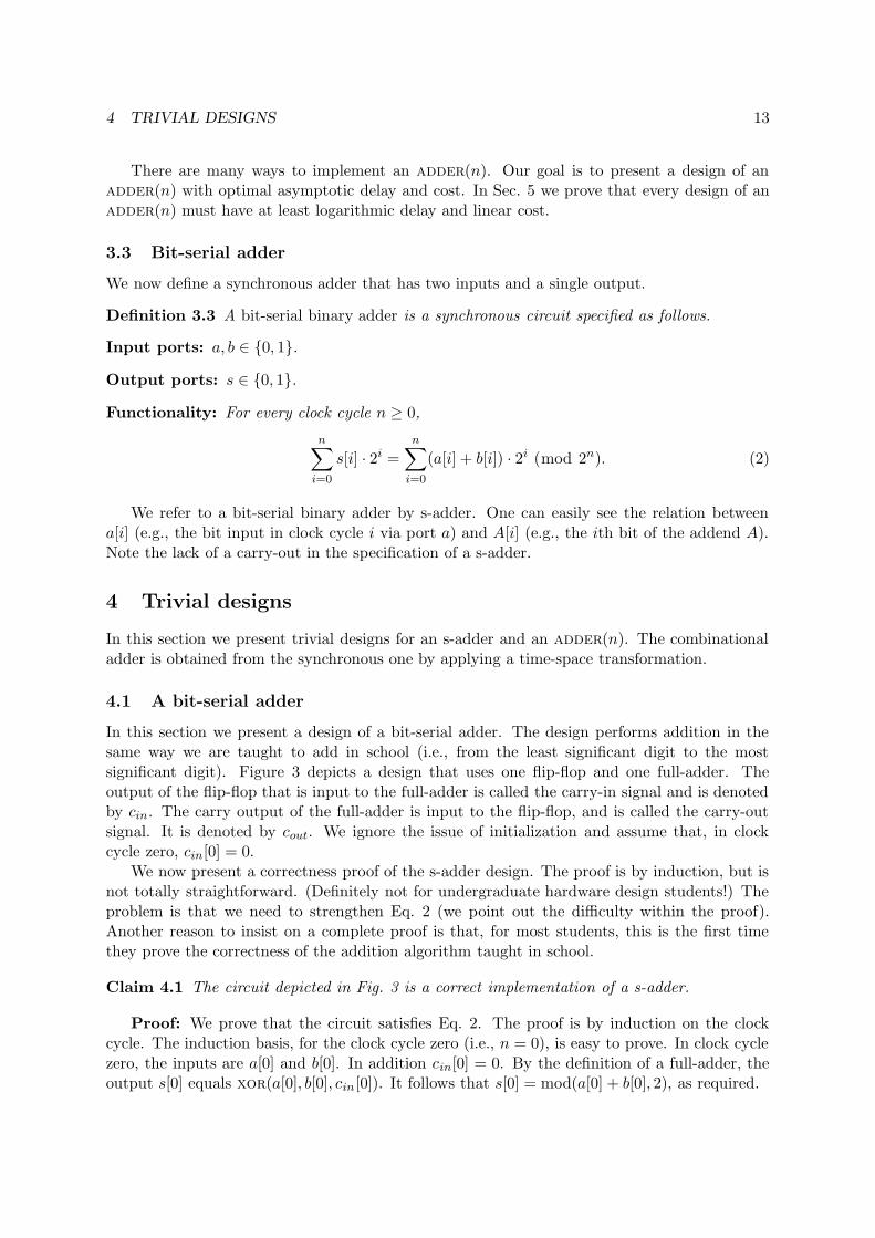
In this section we present a design of a bit-serial adder. The design performs addition in thesame way we are taught to add in school (i.e., from the least significant digit to the mostsignificant digit). Figure 3 depicts a design that uses one flip-flop and one full-adder. Theoutput of the flip-flop that is input to the full-adder is called the carry-in signal and is denotedby cin. The carry output of the full-adder is input to the flip-flop, and is called the carry-outsignal. It is denoted by cout. We ignore the issue of initialization and assume that, in clockcycle zero, cin[0] = 0.
We now present a correctness proof of the s-adder design. The proof is by induction, but isnot totally straightforward. (Definitely not for undergraduate hardware design students!) Theproblem is that we need to strengthen Eq. 2 (we point out the difficulty within the proof).Another reason to insist on a complete proof is that, for most students, this is the first timethey prove the correctness of the addition algorithm taught in school.
Claim 4.1 The circuit depicted in Fig. 3 is a correct implementation of a s-adder.
Proof: We prove that the circuit satisfies Eq. 2. The proof is by induction on the clockcycle. The induction basis, for the clock cycle zero (i.e., n = 0), is easy to prove. In clock cyclezero, the inputs are a[0] and b[0]. In addition cin[0] = 0. By the definition of a full-adder, theoutput s[0] equals xor(a[0], b[0], cin[0]). It follows that s[0] = mod(a[0] + b[0], 2), as required.
4 TRIVIAL DESIGNS 14
a b
clkff
cs
s
cout
cin
fa
Figure 3: A schematic of a serial adder.
We now try to prove the induction step for n + 1. Surprisingly, we are stuck. If we tryto apply the induction hypothesis to the first n cycles, then we cannot claim anything aboutcin[n + 1]. (We do know that cin[n + 1] = cout[n], but Eq. 2 does not tell us anything aboutthe value of cout[n].) On the other hand we cannot apply the induction hypothesis to the lastn cycles (by decreasing the indexes of clock cycles by one) because cin[1] might equal 1.
The way to overcome this difficulty is to strengthen the statement we are trying to prove.Instead of Eq. 2, we prove the following stronger statement: For every clock cycle n ≥ 0,
2n+1 · cout[n] +
n∑
i=0
s[i] · 2i =
n∑
i=0
(a[i] + b[i]) · 2i. (3)
We prove Equation 3 by induction. When n = 0, Equation 3 follows from the functionalityof a full-adder and the assumption that cin[0] = 0. So now we turn again to the induction step,namely, we prove that Eq. 3 holds for n + 1.
The functionality of a full-adder states that
2 · cout[n + 1] + s[n + 1] = a[n + 1] + b[n + 1] + cin[n + 1]. (4)
We multiply both sides of Eq. 4 by 2n+1 and add it to Eq. 3 to obtain
2n+2 · cout[n + 1] + 2n+1 · cout[n] +n+1∑
i=0
s[i] · 2i = 2n+1 · cin[n + 1] +n+1∑
i=0
(a[i] + b[i]) · 2i. (5)
The functionality of the flip-flop implies that cout[n] = cin[n + 1], and hence, Eq. 3 holds alsofor n + 1, and the claim follows. 2
4.2 Ripple-carry adder
In this section we present a design of a combinational adder adder(n). The design we present iscalled a ripple-carry adder. We abbreviate and refer to a ripple-carry adder for binary numbersof length n as rca(n). Although designing an rca(n) from scratch is easy, we obtain it byapplying a transformation, called a time-space transformation, to the bit-serial adder.
Ever since Ami Litman and my father introduced me to retiming [LeiSaxe81, LeiSaxe91,EvenLitman91, EvenLitman94], I thought it is best to describe designs by functionality pre-serving transformations. Namely, instead of obtaining a new design from scratch, obtain it
4 TRIVIAL DESIGNS 15
by transforming a known design. Correctness of the new design follows immediately if thetransformation preserves functionality. In this way a simple design evolves into a sophisticateddesign with much better performance. Students are rarely exposed to this concept, so I choseto present the ripple-carry adder as the outcome of a time-space transformation applied to theserial adder.
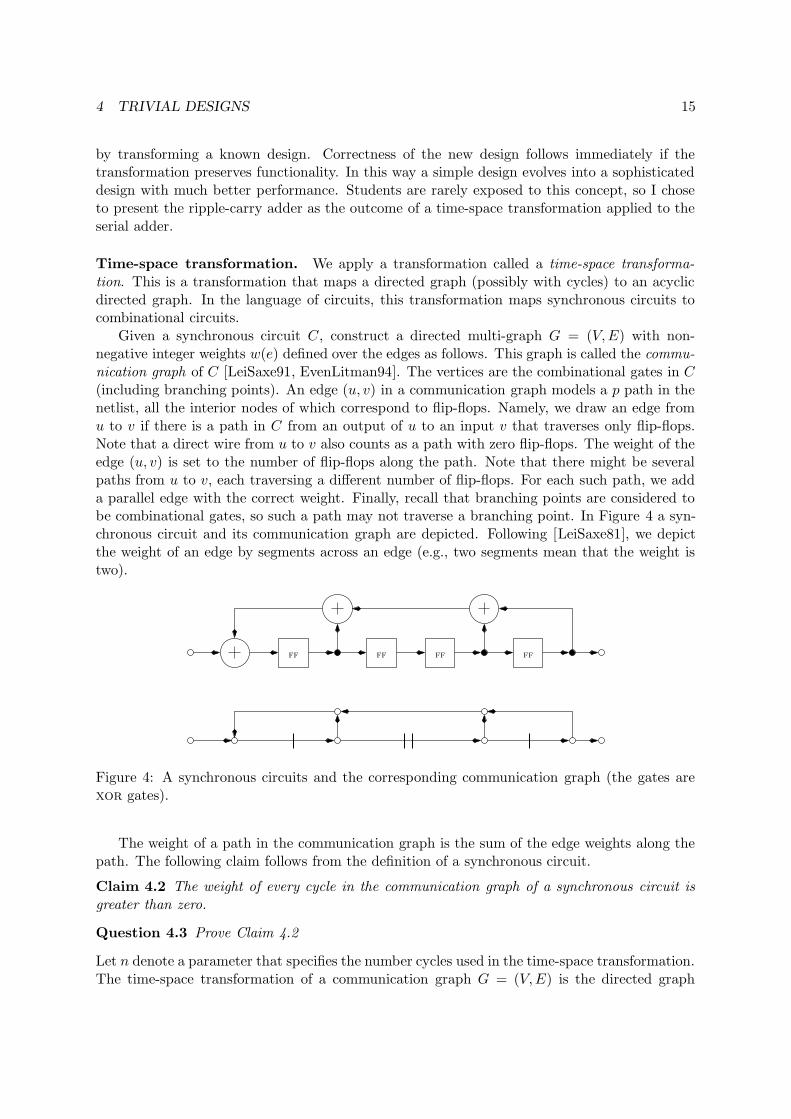
Time-space transformation. We apply a transformation called a time-space transforma-tion. This is a transformation that maps a directed graph (possibly with cycles) to an acyclicdirected graph. In the language of circuits, this transformation maps synchronous circuits tocombinational circuits.
Given a synchronous circuit C, construct a directed multi-graph G = (V,E) with non-negative integer weights w(e) defined over the edges as follows. This graph is called the commu-nication graph of C [LeiSaxe91, EvenLitman94]. The vertices are the combinational gates in C(including branching points). An edge (u, v) in a communication graph models a p path in thenetlist, all the interior nodes of which correspond to flip-flops. Namely, we draw an edge fromu to v if there is a path in C from an output of u to an input v that traverses only flip-flops.Note that a direct wire from u to v also counts as a path with zero flip-flops. The weight of theedge (u, v) is set to the number of flip-flops along the path. Note that there might be severalpaths from u to v, each traversing a different number of flip-flops. For each such path, we adda parallel edge with the correct weight. Finally, recall that branching points are considered tobe combinational gates, so such a path may not traverse a branching point. In Figure 4 a syn-chronous circuit and its communication graph are depicted. Following [LeiSaxe81], we depictthe weight of an edge by segments across an edge (e.g., two segments mean that the weight istwo).
ffffff ff
Figure 4: A synchronous circuits and the corresponding communication graph (the gates arexor gates).
The weight of a path in the communication graph is the sum of the edge weights along thepath. The following claim follows from the definition of a synchronous circuit.
Claim 4.2 The weight of every cycle in the communication graph of a synchronous circuit isgreater than zero.
Question 4.3 Prove Claim 4.2
Let n denote a parameter that specifies the number cycles used in the time-space transformation.The time-space transformation of a communication graph G = (V,E) is the directed graph
4 TRIVIAL DESIGNS 16
stn(G) = (V × {0, . . . , n − 1}, E ′) defined as follows. The vertex set is the Cartesian productof V and {0, . . . , n− 1}. Vertex (v, i) is a copy of v that corresponds to clock cycle i. There isan edge from (u, i) to (v, j) if: (i) (u, v) ∈ E, and (ii) w(u, v) = j − i. The edge ((u, i), (v, j))corresponds to the data transmitted from u to v in clock cycle i. Since there are w(u, v) flip-flopsalong the path, the data arrives to v only in clock cycle j = i + w(u, v).
Since the weight of every directed cycle in G is greater than zero, it follows that st n(G) isacyclic. We now build a combinational circuit Cn whose communication graph is stn(G). Thisis done by placing a gate of type v for each vertex (v, i). The connections use the same portsas they do in C.
There is a boundary problem that we should address. Namely, what feeds input ports ofvertices (v, j) that “should” be fed by a vertex (u, i) with a negative index i? We encounter asimilar problem with output ports of a vertex (u, i) that should feed a vertex (v, j) with an indexj ≥ n. We solve this problem by adding input gates that feed vertices (v, j) where j < w(u, v).Similarly, we add output gates that are fed by vertices (u, i) where i + w(u, v) > n.
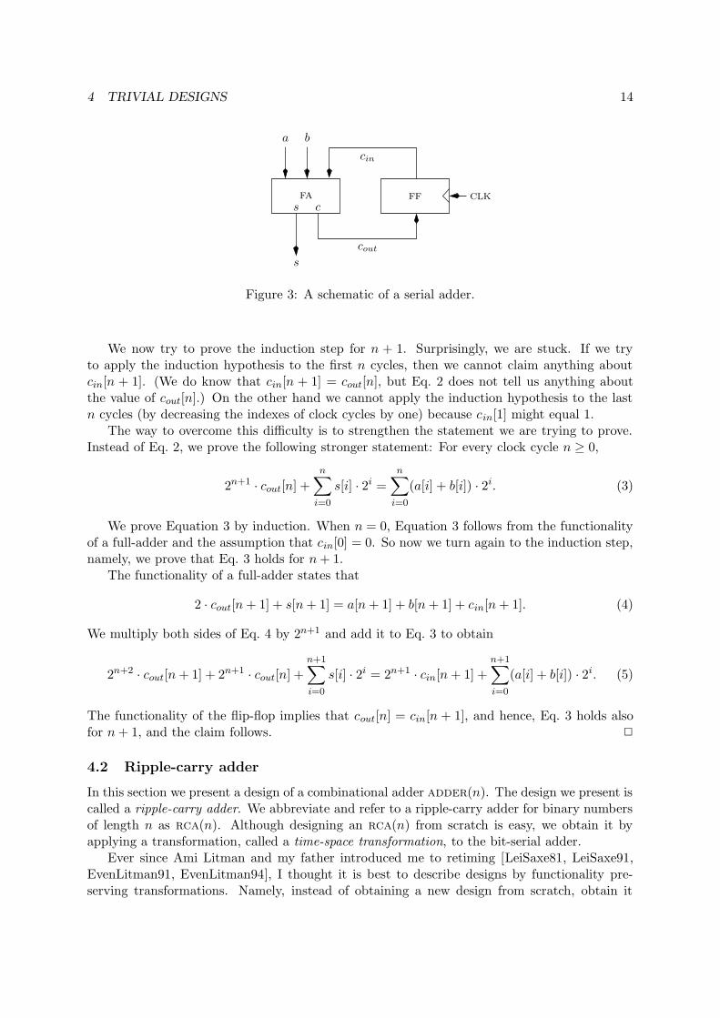
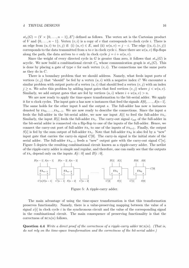
We are now ready to apply the time-space transformation to the bit-serial adder. We applyit for n clock cycles. The input gate a has now n instances that feed the signals A[0], . . . , A[n−1].The same holds for the other input b and the output s. The full-adder has now n instancesdenoted by fa0, . . . , fan−1. We are now ready to describe the connections. Since the input afeeds the full-adder in the bit-serial adder, we now use input A[i] to feed the full-adder fai.Similarly, the input B[i] feeds the full-adder fai. The carry-out signal cout of the full-adder inthe bit-serial adder is connected via a flip-flop to one of the inputs of the full-adder. Hence, weconnect the carry-out port of full-adder fai to one of the inputs of fai+1. Finally, the outputS[i] is fed by the sum output of full-adder fai. Note that full-adder fa0 is also fed by a “new”input gate that carries the carry-in signal C[0]. The carry-in signal is the initial state of theserial adder. The full-adder fan−1 feeds a “new” output gate with the carry-out signal C[n].Figure 5 depicts the resulting combinational circuit known as a ripple-carry adder. The netlistof the ripple-carry adder is simple and regular, and therefore, one can easily see that the outputsof fai depend only on the inputs A[i : 0] and B[i : 0].
scfa0
S[0]
A[0]B[0]
scfa1
A[1]B[1]
C[2] S[1]C[n − 2]
scfa
n−2sc
fan−1
S[n − 2]C[n − 1]S[n − 1]C[n] C[1]
A[n − 2]B[n − 2]A[n− 1]B[n− 1]
C[0]
Figure 5: A ripple-carry adder.
The main advantage of using the time-space transformation is that this transformationpreserves functionality. Namely, there is a value-preserving mapping between the value of asignal x[i] in clock cycle i in the synchronous circuit and the value of the corresponding signalin the combinational circuit. The main consequence of preserving functionality is that thecorrectness of rca(n) follows.
Question 4.4 Write a direct proof of the correctness of a ripple-carry adder rca(n). (That is,do not rely on the time-space transformation and the correctness of the bit-serial adder.)
5 LOWER BOUNDS 17
4.3 Cost and Delay
The bit-serial adder consists of a single full-adder and a single bit flip-flop. It follows that thecost of the bit-serial adder is constant. The addition of n-bit numbers requires n clock cycles.
The ripple-carry adder rca(n) consists of n full-adders. Hence, its cost is linear in n. Thedelay is also linear since the path from A[0] to S[n− 1] traverses all the n full-adders.
5 Lower bounds
We saw that rca(n) has a linear cost and a linear delay. Before we look for better adder designs,we address the question of whether there exist cheaper or faster adders. For this purpose weneed to prove lower bounds.
Lower bounds are rather mysterious to many students. One reason is mathematical innature; students are not used to arguing about unknown abstract objects. The only lowerbound that they probably encountered so far is the lower bound on the number of comparisonsneeded for sorting. Another reason is that they have been noticing a continuous improvementin computer performance and an ongoing reduction in computer costs. So many students areunder the impression that there is no limit to faster and cheaper circuits. This impression mightbe even “well founded” if they heard about “Moore’s Law”. Finally, they are accustomed tothinking that better ways are awaiting the ingenious or lucky inventor.
We first state the lower bounds for the delay and cost of binary adders.
Theorem 5.1 Assume that the number of inputs of every combinational gate is bounded byc. Then, for every combinational circuit G that implements an adder(n), the following hold:c(G) ≥ n/c and d(G) ≥ logc n.
How does one prove this theorem? The main difficulty is that we are trying prove somethingabout an unknown circuit. We have no idea whether there exist better ways to add. Perhapssome strange yet very simple Boolean function of certain bits of the addends can help uscompute the sum faster or cheaper? Instead of trying to consider all possible methods fordesigning adders, we rely on the simplest properties that every adder must have. In fact, theproof is based on topological properties common to every adder. There are two topologicalproperties that we use: (i) There must be a path from every input to the output S[n − 1].(ii) The number of inputs of every combinational gate is bounded by c. Hence the proof ofTheorem 5.1 reveals an inherent limitation of combinational circuits rather than incompetenceof designers.
Question 5.2 Prove Theorem 5.1.Hint: Show that the output bit S[n] depends on all the inputs. This means that one cannot
determine the value of S[n] without knowing the values of all the input bits. Prove that inevery combinational circuit in which the output depends on all the inputs the delay is at leastlogarithmic and the cost is at least linear in the number of inputs. Rely on the fact that thenumber of inputs of each gate is at most c.
Returning the ripple-carry adder rca(n), we see that its cost is optimal (upto a constant).However, its delay is linear. The lower bound is logarithmic, so much faster adders might exist.We point out that, in commercial microprocessors, 32-bit numbers are easily added within a
6 THE ADDER OF LADNER AND FISCHER 18
single clock cycle. (In fact, in some floating point units numbers over 100 bits long are addedwithin a clock cycle.) Clock periods in contemporary microprocessors are rather short; theyare shorter than 10 times the delay of a full-adder. This means that even the addition of 32-bitnumbers within one clock cycle requires faster adders.
6 The adder of Ladner and Fischer
In this section we present an adder design whose delay and cost are asymptotically optimal (i.e.,logarithmic delay and linear cost).
6.1 Motivation
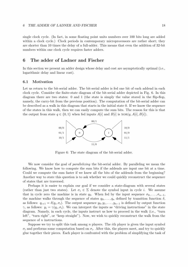
Let us return to the bit-serial adder. The bit-serial adder is fed one bit of each addend in eachclock cycle. Consider the finite-state diagram of the bit-serial adder depicted in Fig. 6. In thisdiagram there are two states: 0 and 1 (the state is simply the value stored in the flip-flop,namely, the carry-bit from the previous position). The computation of the bit-serial adder canbe described as a walk in this diagram that starts in the initial state 0. If we know the sequenceof the states in this walk, then we can easily compute the sum bits. The reason for this is thatthe output from state q ∈ {0, 1} when fed inputs A[i] and B[i] is xor(q,A[i], B[i]).
0 1
00/0
01/1
10/1
10/0
01/0
11/1
00/1
11/0
Figure 6: The state diagram of the bit-serial adder.
We now consider the goal of parallelizing the bit-serial adder. By paralleling we mean thefollowing. We know how to compute the sum bits if the addends are input one bit at a time.Could we compute the sum faster if we knew all the bits of the addends from the beginning?Another way to state this question is to ask whether we could quickly reconstruct the sequenceof states that are traversed.
Perhaps it is easier to explain our goal if we consider a state-diagram with several states(rather than just two states). Let σi ∈ Σ denote the symbol input in cycle i. We assumethat in cycle zero the machine is in state q0. When fed by the input sequence σ0, . . . , σn−1,the machine walks through the sequence of states q0, . . . , qn defined by transition function δ,as follows: qi+1 = δ(qi, σi). The output sequence y0, y1, . . . , yn−1 is defined by output functionγ, as follows: yi = γ(qi, σi). We can interpret the inputs as “driving instructions” in the statediagram. Namely, in each cycle, the inputs instruct us how to proceed in the walk (i.e., “turnleft”, “turn right”, or “keep straight”). Now, we wish to quickly reconstruct the walk from thesequence of n instructions.
Suppose we try to split this task among n players. The ith player is given the input symbolσi and performs some computation based on σi. After this, the players meet, and try to quicklyglue together their pieces. Each player is confronted with the problem of simplifying the task of
6 THE ADDER OF LADNER AND FISCHER 19
gluing. The main obstacle is that each player does not know the state qi of the machine whenthe input symbol σi is input. At first, it seems that knowing qi is vital if, for example, playersi and i + 1 want to combine forces.
Ladner and Fisher proposed the following approach. Each player i computes (or, moreprecisely chooses) a restricted transition function δi : S → S, defined by δi(q) = δ(q, σi). Onecan obtain a “graph” of δi if one considers only the edges in the state diagram that are labeledwith the input symbol σi. By definition, if the initial state is q0, then q1 = δ0(q0). In general,qi = δi−1(qi−1), and hence, qi = δi−1(δi−2(· · · (δ0(q0)) · · · ). It follows that player i is satisfiedif she computes the composition of the functions δi−1, . . . , δ0. Note that the function δi isdetermined by the input symbol σi, and the functions δi are selected from a fixed collection of|Σ| functions.
Before we proceed, there is a somewhat confusing issue that we try to clarify. We usuallythink of an input σi as a parameter that is given to a function (say, f), and the goal is to evaluatef(σ). Here, the input σi is used to select a function δi. We do not evaluate the function δi;instead, we compose it with other functions.
We denote the composition of two function f and g by f ◦ g. Note that (f ◦ g)(q)4= f(g(q)).
Namely, g is applied first, and f is applied second.We denote the composition of the functions δi, . . . , δ0 by the function πi. Namely, π0 = δ0,
and πi+1(q) = δi+1(πi(q)). Assume that, given representations of two functions f and g, therepresentation of the composition f ◦ g can be computed in constant time. This implies thatthe function πn−1 can be, of course, computed with linear delay. The goal in parallelizing thecomputation is to compute πn−1 with logarithmic delay. Moreover, we wish to compute all thefunctions π0, . . . , πn−1 with logarithmic delay and with overall linear cost.
Recall that our goal is to compute the output sequence rather than the sequence of statestraversed by the state machine. Obviously, if we compute the walk q0, . . . , qn−1, then we caneasily compute the output sequence simply by yi = γ(qi, σi). Hence, each output symbol yi
can be computed with constant delay and cost after qi is computed. This means that we havereduced the problem of parallelizing the computation of a finite state machine to the problemof parallelizing the computation of compositions of functions.
Remember that our goal is to design an optimal adder. So the finite state machine we areinterested in is the bit-serial adder. There are four possible input symbols corresponding to thevalues of the bits a[i] and b[i]. The definition of full-adder (and the state diagram), imply thatthe function δi satisfies the following condition for q ∈ {0, 1}:
δi(q) =
{
0 if q + a[i] + b[i] < 2
1 if q + a[i] + b[i] ≥ 2.
=
0 if a[i] + b[i] = 0
q if a[i] + b[i] = 1.
1 if a[i] + b[i] = 2.
(6)
In the literature the sum a[i]+b[i] is often represented using the carry “kill/propagate/generate”signals [CLR90]. This terminology is justified by the following explanation.
• When a[i]+ b[i] = 0, it is called “kill”, because the carry-out is zero. In Eq. 6, we see thatwhen a[i] + b[i] = 0, the value of the function δi is always zero.

6 THE ADDER OF LADNER AND FISCHER 20
• When a[i] + b[i] = 1, it is called “propagate”, because the carry-out equals the carry-in.In Eq. 6, we see that when a[i] + b[i] = 1, the function δi is the identity function.
• When a[i] + b[i] = 2, it is called “generate”, because the carry-out is one. In Eq. 6, we seethat when a[i] + b[i] = 2, the value of the function δi is always one.
From this discussion, it follows that the “kill/propagate/generate” jargon (also known ask, p, g) is simply a representation of a[i] + b[i]. We prefer to abandon this tradition and use adifferent notation described below.
Equation 6 implies that, in a bit-serial adder, δi can be one of three functions: the zerofunction (i.e., value is always zero), the one function (i.e., value is always one), and the identityfunction (i.e., value equals the parameter). We denote the zero function by f0, the one functionby f1, and the identity function by fid.
The fact that these three functions are closed under composition can be easily verified sincefor every x ∈ {0, id, 1}:
f0 ◦ fx = f0
fid ◦ fx = fx
f1 ◦ fx = f1.
Finally, we point out that the “multiplication” table presented for the operator defined overthe alphabet {k, p, g} is simply the table of composing the functions f0, fid, f1 (see, for example,[CLR90]).
6.2 Associativity of composition
Before we continue, we point out an important property of compositions of functions whosedomain and range are identical (e.g., Q is both the domain and the range of all the functionsδi).
Consider a set Q and the set F of all functions from Q to Q. An operator is a function? : F × F → F . (One could define operators ? : A × A → A with respect to any set A. Herewe need only operators with respect to F .) Since ? is a dyadic function, we denote by f ? g theimage of ? when applied to f and g.
Composition of functions is perhaps the most natural operator. Given two functions, f, g ∈F , the composition of f and g is the function h defined by h(q) = f(g(q)). We denote thecomposition of f and g by f ◦ g.
Definition 6.1 An operator ? : F ×F → F is associative if, for every three functions f, g, h ∈F , the following holds:
(f ? g) ? h = f ? (g ? h).
We note that associativity is usually defined for dyadic functions, namely, f(a, f(b, c)) =f(f(a, b), c). Here, we are interested in operators (i.e., functions of functions), so we considerassociativity of operators. Of course, associativity means the same in both cases, and one shouldnot be confused by the fact that the value of an operator is a function.
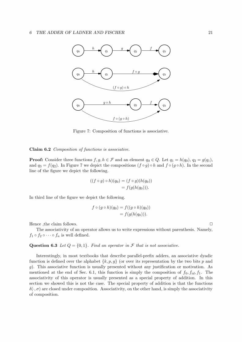
We wish to prove that composition is an associative operator. Although this is an easy claim,it is often hard to convince the students that it is true. One could prove this by a reduction tomultiplication of zero-one matrices. Instead, we provide a “proof by diagram”.
6 THE ADDER OF LADNER AND FISCHER 21
q0 q1 q2 q3
h g f
q0 q3q2
q0 q3
f ◦ (g ◦ h)
q1
f ◦ g
(f ◦ g) ◦ h
h
fg ◦ h
Figure 7: Composition of functions is associative.
Claim 6.2 Composition of functions is associative.
Proof: Consider three functions f, g, h ∈ F and an element q0 ∈ Q. Let q1 = h(q0), q2 = g(q1),and q3 = f(q2). In Figure 7 we depict the compositions (f ◦ g) ◦ h and f ◦ (g ◦ h). In the secondline of the figure we depict the following.
((f ◦ g) ◦ h)(q0) = (f ◦ g)(h(q0))
= f(g(h(q0))).
In third line of the figure we depict the following.
f ◦ (g ◦ h)(q0) = f((g ◦ h)(q0))
= f(g(h(q0))).
Hence ,the claim follows. 2
The associativity of an operator allows us to write expressions without parenthesis. Namely,f1 ◦ f2 ◦ · · · ◦ fn is well defined.
Question 6.3 Let Q = {0, 1}. Find an operator in F that is not associative.
Interestingly, in most textbooks that describe parallel-prefix adders, an associative dyadicfunction is defined over the alphabet {k, p, g} (or over its representation by the two bits p andg). This associative function is usually presented without any justification or motivation. Asmentioned at the end of Sec. 6.1, this function is simply the composition of f0, fid, f1. Theassociativity of this operator is usually presented as a special property of addition. In thissection we showed this is not the case. The special property of addition is that the functionsδ(·, σ) are closed under composition. Associativity, on the other hand, is simply the associativityof composition.
6 THE ADDER OF LADNER AND FISCHER 22
6.3 The parallel prefix problem
In Section 6.1, we reduced the problem of designing a fast adder to the problem of comput-ing compositions of functions. In Section 6.2, we showed that composition of functions is anassociative operator. This motivates the definition of the prefix problem.
Definition 6.4 Consider a set A and an associative operator ? : A × A → A. The prefixproblem is defined as follows.
Input: δ0, . . . , δn−1 ∈ A.
Output: π0, . . . , πn−1 ∈ A defined by π0 = δ0 and πi = δi ? · · · ? δ0, for 0 < i < n. (Note thatπi+1 = δi+1 ? πi.)
Assume that we have picked a (binary) representation for elements in A. Moreover, assumethat we have an implementation of the associative operator ? with respect to this implementa-tion. Namely, a ?-gate is a combinational gate that when fed two representations of elementsf, g ∈ A, outputs a representation of f ? g. Our goal now is to design a fast circuit for solvingthe prefix problem using ?-gates. Namely, our goal is to design a parallel prefix circuit.
Note that the operator ? need not be commutative, so the inputs of the ?-gate cannot beinterchanged. This means that there is a difference between the left input and the right inputof a ?-gate.
6.4 The parallel prefix circuit
We are now ready to describe a combinational circuit for the prefix problem. We will use onlyone building block, namely, a ?-gate. We assume that the cost and the delay of a ?-gate areconstant (i.e., do not depend on n).
We begin by considering two circuits; one with optimal cost and the second with optimaldelay. We then present a circuit with optimal cost and delay.
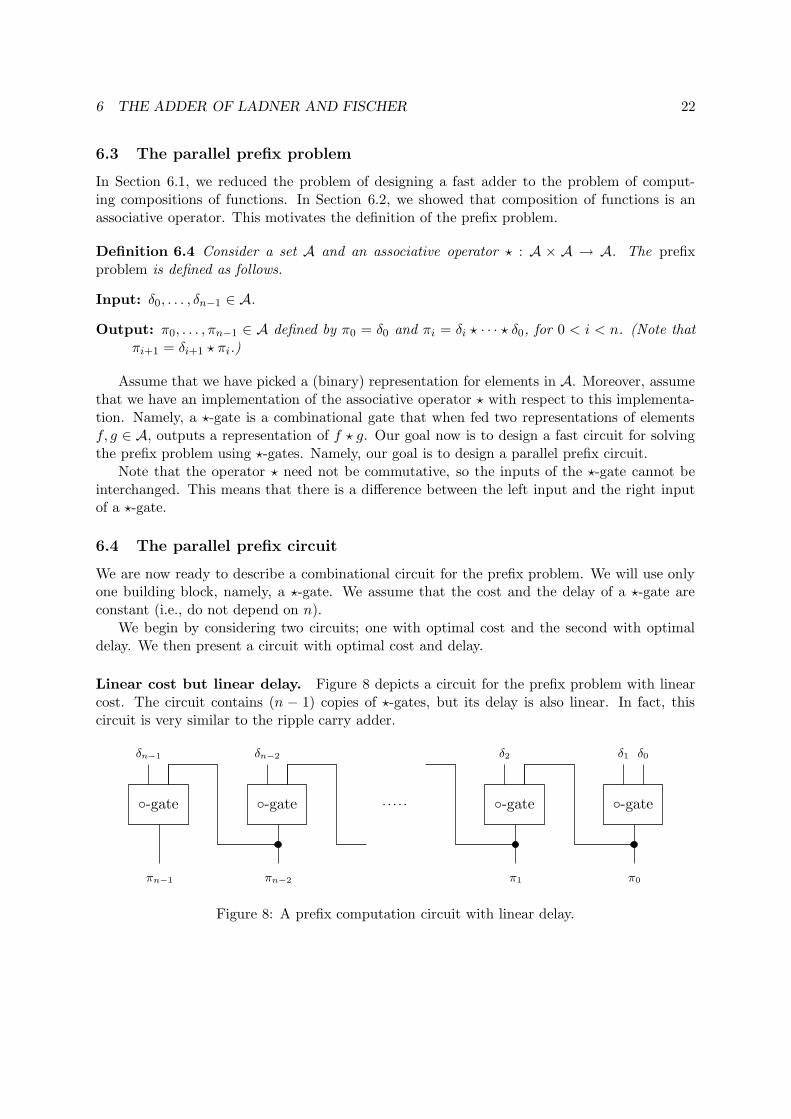
Linear cost but linear delay. Figure 8 depicts a circuit for the prefix problem with linearcost. The circuit contains (n − 1) copies of ?-gates, but its delay is also linear. In fact, thiscircuit is very similar to the ripple carry adder.
◦-gate
δn−1
πn−1
◦-gate
δn−2
πn−2
◦-gate
δ2
π1
◦-gate
δ1 δ0
π0
Figure 8: A prefix computation circuit with linear delay.
6 THE ADDER OF LADNER AND FISCHER 23
Logarithmic delay but quadratic cost. The ith output πi can be computed by circuitwith the topology of a balanced binary tree, where the inputs are fed from the leaves, a ?-gateis placed in each node, and πi is output by the root. The circuit contains (i−1) copies of ?-gatesand its delay is logarithmic in i. We could construct a separate tree for each πi to obtain ncircuits with logarithmic delay but quadratic cost.
Our goal now is to design a circuit with logarithmic delay and linear cost. Intuitively,the design based on n separate trees is wasteful because the same computations are repeatedin different trees. Hence, we need to find an efficient way to “combine” the trees so thatcomputations are not repeated.
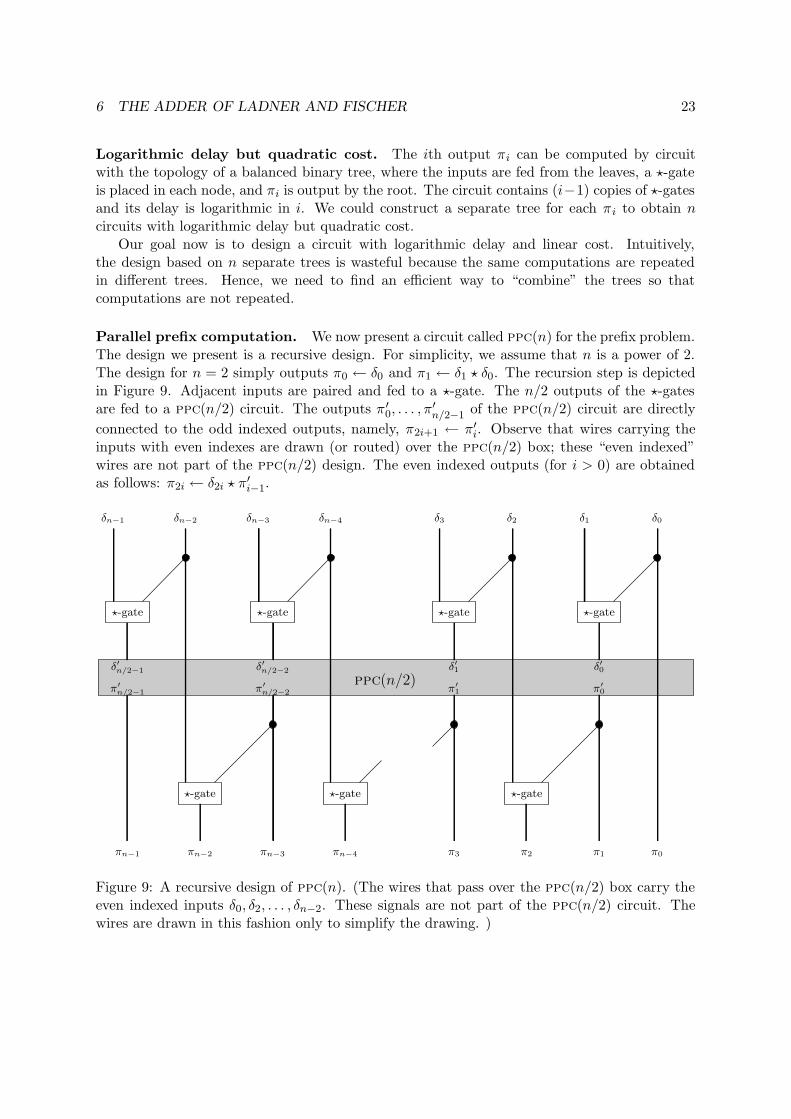
Parallel prefix computation. We now present a circuit called ppc(n) for the prefix problem.The design we present is a recursive design. For simplicity, we assume that n is a power of 2.The design for n = 2 simply outputs π0 ← δ0 and π1 ← δ1 ? δ0. The recursion step is depictedin Figure 9. Adjacent inputs are paired and fed to a ?-gate. The n/2 outputs of the ?-gatesare fed to a ppc(n/2) circuit. The outputs π ′
0, . . . , π′n/2−1
of the ppc(n/2) circuit are directly
connected to the odd indexed outputs, namely, π2i+1 ← π′i. Observe that wires carrying the
inputs with even indexes are drawn (or routed) over the ppc(n/2) box; these “even indexed”wires are not part of the ppc(n/2) design. The even indexed outputs (for i > 0) are obtainedas follows: π2i ← δ2i ? π′
i−1.
?-gate?-gate?-gate
?-gate?-gate?-gate?-gate
π0
δ0δ1δ2δ3δn−4δn−3δn−2δn−1
π1π2π3πn−4πn−3πn−2πn−1
δ′
n/2−1δ′
n/2−2δ′
1 δ′
0
π′
n/2−1π′
n/2−2π′
1 π′
0
ppc(n/2)
Figure 9: A recursive design of ppc(n). (The wires that pass over the ppc(n/2) box carry theeven indexed inputs δ0, δ2, . . . , δn−2. These signals are not part of the ppc(n/2) circuit. Thewires are drawn in this fashion only to simplify the drawing. )
6 THE ADDER OF LADNER AND FISCHER 24
6.5 Correctness
Claim 6.5 The design depicted in Fig. 9 is correct.
Proof: The proof of the claim is by induction. The induction basis holds trivially for n = 2.We now prove the induction step. Consider the ppc(n/2) used in a ppc(n). Let δ ′i and π′
i denotethe inputs and outputs of the ppc(n/2), respectively. The ith input δ ′[i] equals δ2i+1 ? δ2i. Byassociativity and the induction hypothesis, the ith output π ′
i satisfies:
π′i = δ′i ? · · · δ′0
= (δ2i+1 ? δ2i) ? · · · ? (δ1 ? δ0)
It follows that the output π2i+1 equals the composition δ2i+1 ? · · · ? δ0, as required. Hence, theodd indexed outputs π1, π3, . . . , πn−1 are correct.
Finally, output in position 2i equals δ2i ? π′i−1 = δ2i ? π2i−1 = δ2i ? · · · ? δ0. It follows that
the even indexed outputs are also correct, and the claim follows. 2
6.6 Delay and cost analysis
The delay of the ppc(n) circuit satisfies the following recurrence:
d(ppc(n)) =
{
d(?-gate) if n = 2
d(ppc(n/2)) + 2 · d(?-gate) otherwise.
If follows that
d(ppc(n)) = (2 log n− 1) · d(?-gate).
The cost of the ppc(n) circuit satisfies the following recurrence:
c(ppc(n)) =
{
c(?-gate) if n = 2
c(ppc(n/2)) + (n− 1) · c(?-gate) otherwise.
Let n = 2k, it follows that
c(ppc(n)) =
k∑
i=2
(2i − 1) · c(?-gate) + c(?-gate)
= (2n− log n− 2) · c(?-gate).
We conclude with the following corollary.
Corollary 6.6 If the delay and cost of an ?-gate is constant, then
d(ppc(n)) = Θ(log n)
c(ppc(n)) = Θ(n).
Question 6.7 This question deals with the implementation of ◦-gates for general finite statemachines. (Recall that a ◦-gate implements composition of restricted transition functions.)
6 THE ADDER OF LADNER AND FISCHER 25
1. Suggest a representation (using bits) for the functions δi.
2. Design a ◦-gate with respect to your representation, namely, explain how to compute com-position of functions in this representation.
3. What is the size and delay of the ◦-circuit with this representation? How does it dependon Q and Σ?
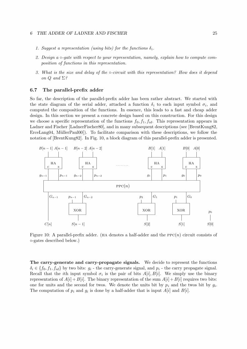
6.7 The parallel-prefix adder
So far, the description of the parallel-prefix adder has been rather abstract. We started withthe state diagram of the serial adder, attached a function δi to each input symbol σi, andcomputed the composition of the functions. In essence, this leads to a fast and cheap adderdesign. In this section we present a concrete design based on this construction. For this designwe choose a specific representation of the functions f0, f1, fid. This representation appears inLadner and Fischer [LadnerFischer80], and in many subsequent descriptions (see [BrentKung82,ErceLang04, MullerPaul00]). To facilitate comparison with these descriptions, we follow thenotation of [BrentKung82]. In Fig. 10, a block diagram of this parallel-prefix adder is presented.
p1
S[1]
p2
S[2]
p0p1pn−2pn−1 g0g1gn−2gn−1
pn−1
S[n − 1]C[n] S[0]
p0
G0G1Gn−2Gn−1
xorxorxor
A[0]B[0]
scha
A[1]B[1]
schaha
A[n− 2]B[n − 2]A[n− 1]B[n− 1]
ppc(n)
scha
sc
Figure 10: A parallel-prefix adder. (ha denotes a half-adder and the ppc(n) circuit consists of◦-gates described below.)
The carry-generate and carry-propagate signals. We decide to represent the functionsδi ∈ {f0, f1, fid} by two bits: gi - the carry-generate signal, and pi - the carry propagate signal.Recall that the ith input symbol σi is the pair of bits A[i], B[i]. We simply use the binaryrepresentation of A[i]+B[i]. The binary representation of the sum A[i]+B[i] requires two bits:one for units and the second for twos. We denote the units bit by pi and the twos bit by gi.The computation of pi and gi is done by a half-adder that is input A[i] and B[i].
7 FURTHER TOPICS 26
Implementation of the ◦-gate. Now that we have selected a representation of the functionsf0, f1, fid, we need to design the ◦-gate that implements composition. This is an easy task: if(g, p) = (g1, p1) ◦ (g2, p2), then g = g1 or (p1 and g2) and p = p1 and p2.
Putting things together. The pairs of signals (g0, p0), (g1, p1), . . . (gn−1, pn−1) are input toa ppc(n) circuit that contains only ◦-gates. The output of the ppc(n) is a representation of thefunctions πi, for 0 ≤ i < n. We denote the pair of bits used to represent πi by (Gi, Pi). We donot need the outputs P0, . . . , Pn−1, so we only depict the outputs G0, . . . , Gn−1.
Recall that state qi+1 equals πi(q0). Since q0 = 0, it follows that πi(q0) = 1 if and only ifπi = f1, namely, if and only if Gi = 1. Hence qi+1 = Gi.
We are now ready to compute the sum bits: Since S[0] = xor(A[0], B[0]), we may reusep[0], and output S[0] = p[0]. For 0 < i < n, S[i] = xor(A[i], B[i], qi) = xor(pi, Gi−1). Finally,for those interested in the carry-out bit C[n], simply note that C[n] = qn = Gn−1.
Question 6.8 Compute the number of gates of each type in the parallel prefix adder presentedin this chapter as a function of n.
In fact it is possible to save some hardware by using degenerate ◦-gates when only thecarry-generate bit of the output of a ◦-gate is used. This case occurs for the n/2 − 1 ◦-gateswhose outputs only feed outputs of the ppc(n) circuit. More generally, one could define suchdegenerate ◦-gates recursively, as follows. A ◦-gate is degenerate if: (i) Its output feeds onlyan output of the ppc(n) circuit, or (ii) Its output is connected only to ports that are the rightinput ports of degenerate ◦-gates or an output port of the ppc(n)-circuit.
Question 6.9 How many degenerate ◦-gates are there?
7 Further topics
In this section we discuss various topics related to adders,
7.1 The carry-in bit
The role of the carry-in bit is somewhat mysterious at this stage. To my knowledge, no pro-gramming language contains an instruction that uses a carry-in bit. For example, we writeS := A + B, and we do not have an extra single bit variable for the carry-in. So why is thecarry-in included in the specification of an adder?
There are two justifications for the carry-in bit. The first justification is that one can buildadders of numbers of length k + ` by serially connecting an adder of length k and an adder oflength `. The carry-out output of the adder of the lower bits is fed to the carry-in inputs of theadder of the higher bits.
A more important justification for the carry-in bit is that it is needed for a constant timereduction from subtraction of two’s complement numbers to binary addition. A definition of thetwo’s complement representation and a proof of the reduction appear in [MullerPaul00, Even04].
In this essay, we do not define two’s complement representation or deal with subtraction.However, most hardware design courses deal with these issues, and hence, they need the carry-ininput. The carry-in input creates very little complications, so we do not mind considering it,even if its usefulness is not clear at this point.
7 FURTHER TOPICS 27
Formally, the carry-in bit is part of the input and is denoted by C[0]. The goal is to computeA + B + C[0].
There are three main ways to compute A + B + C[0] within the framework of this essay:
1. The carry-in bit C[0] can be viewed as a setting of the initial state q0. Namely, q0 = C[0].This change has two effects on the parallel-prefix adder design: (i) The sum bit S[0]equals γ(q0, σ0). Hence S[0] = xor(C[0], p[0]). (ii) For i > 0, the sum bit S[i] equalsxor(πi−1(q0), pi). Hence S[i] can be computed from 4 bits: pi, C[0], and Gi−1, Pi−1. Thedisadvantage of this solution is that we need an additional gate for the computation ofeach sum bit. The advantage of this solution is that it suggests a simple way to design acompound adder (see Sec. 7.2).
2. The carry-in bit can be viewed as two additional bits of inputs, namely A[−1] = B[−1] =C[0], and then C[0] = 2−1 · (A[−1] + B[−1]). This means that we reduce the task ofcomputing A + B + C[0] to the task of adding numbers that are longer by one bit. Thedisadvantage of this solution is that the ppc(n) design is particularly suited for n that isa power of two. Increasing n (that is a power of two) by one incurs a high overhead incost.
3. Use δ′0 instead of δ0, where δ′0 is defined as follows:
δ′04=
{
f0 if A[0] + B[0] + C[0] < 2
f1 if A[0] + B[0] + C[0] ≥ 2.
This setting avoids the assignment δ0 = fid, but still satisfies: δ′0(q0) = q1 since q0 = C[0].Hence, the ppc(n) circuit outputs the correct functions even when δ0 is replaced by δ′0.The sum bit S[0] is computed directly by xor(A[0], B[0], C[0]).
Note that the implementation simply replaces the half-adder used to compute p0 and g0
by a full-adder that is also input C[0]. Hence, the overhead for dealing with the carry-inbit C[0] is constant.
7.2 Compound adder
A compound adder is an adder that computes both A + B and A + B + 1. Compound addersare used in floating point units to implement rounding. Interestingly, one does not need twocomplete adders to implement a compound adder since hardware can be shared. On the otherhand, this method does not allow using a ppc(n) circuit with degenerate ◦-gates.
The idea behind sharing is that, in the first method way for computing A + B + C[0], wedo not rely on the carry-in C[0] to compute the functions πi. Only after the functions πi arecomputed, the carry-in bit C[0] is used to determine the initial state q0. The sum bits thensatisfy S[i] = xor(πi−1(q0), pi), for i > 0. This means that we can share the circuitry thatcomputes πi for the computation of the sum A + B and the incremented sum A + B + 1.
7.3 Fanout
The fanout of a circuit is the maximum fanout of an output port in the circuit. Recall thatthe fanout of an output port is the number of input ports that are connected to it. In reality,a large fanout slows down the circuit. The main reason for this in CMOS technology is that
7 FURTHER TOPICS 28
each input port has a capacity. An output port has to charge (or discharge) all the capacitorscorresponding to the input ports that it feeds. As the capacitance increases linearly with thefanout, the delay associated with stabilizing the output signal also increases linearly with thefanout. So it is desirable to keep the fanout low. (Delay grows even faster if resistance is takeninto account.)
Ladner and Fischer provided a complete analysis of the fanout. In the ppc(n) circuit, theonly cause for fanout greater than 2 are the branchings after the output of ppc(n/2). Namely,only nets that feed outputs have a large fanout. Let fo(i, n) denote the fanout of the net thatfeeds πi. It follows that fo(2i, 2n) = 1 and fo(2i + 1, 2n) = 1 + fo(i, n). Hence, the fanout islogarithmic. Brent and Kung [BrentKung82] reduced the fanout to two but increased the costto O(n log n). One could achieve the same fanout while keeping the cost linear (see questionbelow for details); however, the focus in [BrentKung82] was area and a regular layout, not cost.
Question 7.1 In this question we consider fanout in the ppc(n) design and suggest a way toreduce the fanout so that it is at most two.
• What is the maximum fanout in the ppc(n) design?
• Find the output port with the largest fanout in the ppc(n) circuit.
• The fanout can be made constant if buffers are inserted according to the following recursiverule. Insert a buffer in every branching point of the ppc(n) that is fed by an output ofthe ppc(n/2) design (such branching points are depicted in Fig. 9 by filled circles belowthe ppc(n/2) circuit). (A buffer is a combinational circuit that implements the identityfunction. A buffer can be implemented by cascading two inverters.)
• By how much does the insertion of buffers increase the cost and delay?
• The rule for inserting buffers to reduce the fanout can be further refined to save hardwarewithout increasing the fanout. Can you suggest how?
7.4 Tradeoffs between cost and delay
Ladner and Fischer [LadnerFischer80] present an additional type of “recursive step” for con-structing a parallel prefix circuit. This additional recursive step reduces the delay at the priceof increasing the cost and the fanout. For input length n, Ladner and Fischer suggested log ndifferent circuits. Loosely speaking, in the kth circuit, one performs k recursive steps of thetype we have presented and then log n − k recursive steps of the second type. We refer thereader to [LadnerFischer80] for the details and the analysis.
In the computer arithmetic literature several circuits have been suggested for fast adders. Forexample, Kogge and Stone suggested a circuit with logarithmic delay but its cost is O(n log n).Its asymptotic layout area is the same as the area of the layout suggested by Brent and Kung.More details about other variations and hybrids can be found in [Knowles99, Zimmerman98].
7.5 VLSI area
This essay is about hardware designs of adders. Since such adders are implemented as VLSIcircuits, it makes sense to consider criteria that are relevant to VLSI circuits. With all otherfactors remaining the same, area is more important in VLSI than counting the number of gates.
8 AN OPINIONATED HISTORY OF ADDER DESIGNS 29
By area one means the area required to draw the circuit on a chip. (Note, however, that moregates usually consume more power.)
More about the model for VLSI area can be found in [Shiloach76, Thompson80]. In fact,the first formal research on the area of hardware circuits was done by Yossi Shiloach under thesupervision of my father during the mid 70’s in the Weizmann institute. This research wasmotivated by discussions with the people who were building the second Golem computer usingprinted circuit boards.
In addition to reducing fanout, Brent and Kung “unrolled” the recursive construction de-picted in Fig. 9 and presented a regular layout for adders. The area of this layout is O(n log n).
8 An opinionated history of adder designs
The search for hardware algorithms for addition with short delay started in the fifties. Ercegovacand Lang [ErceLang04] attribute the earliest reference for an adder with a logarithmic delayto Weinberger and Smith [WeinSmith58]. This adder is often referred to as a carry-lookaheadadder. On the other hand, Ladner and Fischer cite Ofman [Ofman63] for a carry-lookaheadadder. In Cormen et. al., it is said that the circuit of Weinberger and Smith required largegates as opposed to Ofman’s design that required constant size gates. So it seems that inmodern terms, the delay of the design of Weinberger and Smith was not logarithmic.
I failed to locate these original papers. However, one can find descriptions of carry-lookaheadadders in [CLR90, ErceLang04, Koren93, Kornerup97]). The topology of a carry-lookaheadadder is a complete tree of degree 4 with log4 n levels (any constant is fine, and 4 is the commonchoice). The data traverses the tree from the leaves to the root and then back to the leaves. Thecarry-lookahead adder is rather complicated and seems to be very specific to addition. Eventhough the delay is logarithmic and the cost is linear, this adder was not the “final word” onadders. In fact, due to its complexity, only the first two layers of the carry-lookahead adder aredescribed in detail in most textbooks (see [Koren93, ErceLang04]).
The conditional-sum adder [Sklansky60] is a simple adder with logarithmic delay. However,its cost is O(n log n). Even worse, it has a linear fanout, so in practice the delay is actuallyO(log2 n). The main justification for the conditional-sum adder is that it is simple.
There was not much progress in the area of adder design till Ladner and Fischer [LadnerFischer80]presented the parallel-prefix adder. Their idea was to design small combinational circuits thatsimulate finite-state machines (i.e., transducers). They reduced this task to a prefix problemover an associative operator. They call a circuit that computes the prefix problem a parallelprefix circuit. When applied to the trivial bit-serial adder (implemented by a two-state finitestate machine), their method yielded a combinational adder with logarithmic delay, linear size,and logarithmic fanout.
In fact, for every n, Ladner and Fischer presented log n different parallel prefix circuits;these designs are denoted by Pk(n), for k = 0, . . . , log n. The description of the circuits usesrecursion. There are two types of recursion steps, the combination of which yields log n differentcircuits. (For simplicity, we assume throughout that n is a power of 2.) All these designs sharea logarithmic delay and a linear cost, however, the constants vary; reduced delay results inincreased size. Ladner and Fischer saw a similarity between Plog n(n) and the carry-lookaheadadder. However, they did not formalize this similarity and resorted to the statement that ‘webelieve that our circuit is essentially the same as the “carry-lookahead” adder’.
Theory of VLSI was at a peak when Ladner and Fischer published their paper. Brent
9 DISCUSSION 30
and Kung [BrentKung82] popularized the parallel-prefix adder by presenting a regular layoutfor the parallel-prefix adder Plog n(n). The layout was obtained by “unrolling” the recursionin [LadnerFischer80]. The area of the layout is O(n log n). In addition, Brent and Kung reducedthe fanout of Plog n(n) to two by inserting buffers. Since they were concerned with area and werenot sensitive to cost, they actually suggested increasing the cost to O(n log n) (see Question 7.1for guidelines regarding the reduction of the fanout while keeping the cost linear.)
The adder presented in Brent and Kung’s paper is specific for addition. The ideas ofparallelizing the computation of a finite-state machine and the prefix problem are not mentionedin [BrentKung82]. This meant that when teaching the Brent-Kung adder, one introduces thecarry-generate and carry-propagate signals (i.e., gi, pi signals) without any motivation (i.e.,it is a way to compute the carry bits, but where does this originate from?). Even worse,the associative operator is magically pulled out of the hat. Using simple and short algebraicarguments, it is shown that applying this operator to a prefix problem leads to the computationof the carry bits. Indeed, the proofs are short, but most students find this explanation hard tofollow. I suspect that the cause of this difficulty is that no meaning is attached to the associativeoperator and to the gi, pi signals.
The prefix problem gained a lot of success in the area of parallel computation. Leighton [Leighton91]presented a parallel prefix algorithm on a binary tree. The presentation is for a synchronousparallel architecture, and hence the computation proceeds in steps. I think that the simplestway to explain the parallel prefix algorithm on a binary tree is as a simulation of Ladner andFischer’s Plog n(n) circuit on a binary tree. In this simulation, every node in the binary treeis in charge of simulating two nodes in Plog n (one before the recursive call and one after therecursive call).
In Cormen et. al. [CLR90], a carry-lookahead adder is presented. This adder is a hybriddesign that combines the presentation of Brent and Kung and the presentation of Leighton. Themain problem with the presentation in [CLR90] is that the topology is a binary tree and datatraverses the tree in both directions (i.e., from the leaves to the root and back to the leaves).Hence, it is not obvious that the design is combinational (although it is). So the presentationin Cormen et. al. introduces an additional cause for confusion. On the other hand, this mightbe the key to explaining Ofman’s adder. Namely, perhaps Ofman’s adder can be viewed as asimulation of Plog n(n) on a binary tree.
9 Discussion
When I wrote this essay, I was surprised to find that in many senses the presentation in [LadnerFischer80]is better than subsequent textbooks on adders (including my own class notes). Perhaps the mainreason for not adopting the presentation in [LadnerFischer80] is that Ladner and Fischer pre-sented two recursion steps. The combination of these steps led to log n designs for parallel prefixcircuits with n arguments (and hence for n-bit adders). Only one of these designs has gainedmuch attention (i.e., the circuit they called Plog n(n)). There are probably two reasons for thesuccess of this circuit: fanout and area. Brent and Kung were successful in reducing the fanoutand presenting a regular layout only for Plog n(n). It seems that these multiple circuits confusedmany who preferred then only to consider the presentation of Brent and Kung. In this essayonly one type of recursion is described for constructing only one parallel prefix circuit, namely,the Plog n(n) circuit.
I can speculate that the arithmetic community was accustomed to the carry-propagate and
REFERENCES 31
carry-generate signals from the carry-lookahead adder. They did not need motivation for it andthe explanation of Ladner and Fischer was forgotten in favor of the presentation of Brent andKung.
Another speculation is that the parallel computation community was interested in describingparallel algorithms on “canonic” graphs such as binary trees and hypercubes (see [Leighton91]).The special graph of Ladner and Fischer did not belong to this family. In hardware design,however, one has usually freedom in selecting the topology of the circuit, so canonic graphs arenot important.
Acknowledgments
I thank Oded Goldreich for motivating me to write this essay. Thanks to his continuous encour-agement, this essay was finally completed. Helpful remarks were provided by Oded Goldreich,Ami Litman and Peter-Michael Seidel. I am grateful for their positive feedback and constructivesuggestions.
References
[BrentKung82] R. P. Brent and H. T. Kung, “Regular Layout for Parallel Adders”,IEEE Trans. Comp., Vol. C-31, no. 3, pp. 260-264. 1982. Available online athttp://web.comlab.ox.ac.uk/oucl/work/richard.brent/pd/rpb060.pdf
[CLR90] T. H. Cormen, C. E. Leiserson, R. L. Rivest, Introduction to Algorithms, The MITPress, 1990.
[ErceLang04] M. D. Ercegovac and T. Lang, Digital Arithmetic, Morgan Kaufmann, 2004.
[Even79] Shimon Even, Graph Algorithms, Computer Science Press, 1979.
[Even04] G. Even, “Lecture Notes in Computer Structure”, manuscript, 2004.
[EvenLitman91] Shimon Even and Ami Litman, “A systematic design and explanation of theAtrubin multiplier”, Sequences II, Methods in Communication, Security and ComputerSciences, R. Capocelli et.al. (Editors), pp. 189-202, Springer-Verlag, 1993.
[EvenLitman94] Shimon Even and Ami Litman. “On the capabilities of systolic systems”, Math-ematical Systems Theory, 27:3-28, 1994.
[HopUll79] John E. Hopcroft and Jeffrey D. Ullman, Introduction to automata theory, lan-guages, and computation, Addison Wesley, 1979.
[Knowles99] S. Knowles, “A Family of Adders” Proceedings of the 14th IEEE Symposiumon Computer Arithmetic, pp 30-34, 1999. (Note that the figures in the publishedproceedings are wrong.)
[Koren93] Israel Koren, Computer Arithmetic Algorithms, Prentice Hall, 1993.
[Kornerup97] Peter Kornerup, “Chapter 2 on Radix Integer Addition”, manuscript, 1997.
REFERENCES 32
[LadnerFischer80] R. Ladner and M. Fischer, “Parallel prefix computation”, J. Assoc. Comput.Mach., 27, pp. 831–838, 1980.
[Leighton91] F. Thomson Leighton, Introduction to parallel algorithms and architectures: array,trees, hypercubes, Morgan Kaufmann, 1991.
[LeiSaxe81] C. E. Leiserson and J. B. Saxe, “Optimizing synchronous systems”, Journal ofVLSI and Computer Systems, 1:41-67, 1983. (Also appeared in Twenty-Second AnnualSymposium on Foundations of Computer Science, pp. 23-36, 1981.)
[LeiSaxe91] C. E. Leiserson and J. B. Saxe. “Retiming synchronous circuitry”. Algorithmica,6(1)5-35, 1991.
[MullerPaul00] S. M. Muller and W. J. Paul, Computer Architecture: complexity and correct-ness, Springer, 2000.
[Ofman63] Yu Ofman, “On the algorithmic complexity of discrete functions”, Sov Phys Dokl,7, pp. 589-591, 1963.
[Shiloach76] Yossi Shiloach, Linear and planar arrangements of graphs, Ph.D. thesis, Dept. ofApplied Mathematics, Weizmann Institute, 1976.
[Sklansky60] J. Sklansky, “An evaluation of several two-summand binary adders”, IRE Trans.on Electronic Computers, EC-9:213-26, 1960.
[Thompson80] Clark David Thompson, A Complexity Theory For VLSI, PhD Thesis, CarnegieMellon University, 1980.
[WeinSmith58] A. Weinberger and J. L. Smith, “A logic for high-speed addition”, Nat. Bur.Stand. Circ., 591:3-12, 1958.
[Zimmerman98] R. Zimmermann, Binary Adder Architectures for Cell-Based VLSI and theirSynthesis, PhD thesis, Swiss Federal Institute of Technology (ETH) Zurich, Hartung-Gorre Verlag, 1998. Available online at http://www.iis.ee.ethz.ch/~zimmi/