observation of topological nodal fermion … of topological nodal fermion semimetal phase in zrsis...
TRANSCRIPT

Observation of Topological Nodal Fermion Semimetal Phase in ZrSiS
Madhab Neupane,1 Ilya Belopolski,2 M. Mofazzel Hosen,1 Daniel S. Sanchez,2 Raman Sankar,3
Maria Szlawska,4 Su-Yang Xu,2 Klauss Dimitri,1 Nagendra Dhakal,1 Pablo Maldonado,5 Peter M.
Oppeneer,5 Dariusz Kaczorowski,4 Fangcheng Chou,3 M. Zahid Hasan,2 and Tomasz Durakiewicz6
1Department of Physics, University of Central Florida, Orlando, Florida 32816, USA2Joseph Henry Laboratory and Department of Physics,
Princeton University, Princeton, New Jersey 08544, USA3Center for Condensed Matter Sciences, National Taiwan University, Taipei 10617, Taiwan
4Institute of Low Temperature and Structure Research,Polish Academy of Sciences, 50-950 Wroclaw, Poland
5Department of Physics and Astronomy, Uppsala University, P. O. Box 516, S-75120 Uppsala, Sweden.6Condensed Matter and Magnet Science Group, Los Alamos National Laboratory, Los Alamos, NM 87545, USA
(Dated: April 5, 2016)
Unveiling new topological phases of matter is one of the current objectives in condensed matterphysics. Recent experimental discoveries of Dirac and Weyl semimetals prompt to search for otherexotic phases of matter. Here we present a systematic angle-resolved photoemission spectroscopy(ARPES) study of ZrSiS, a prime topological nodal semimetal candidate. Our wider Brillouin zone(BZ) mapping shows multiple Fermi surface pockets such as the diamond-shaped Fermi surface,ellipsoidal-shaped Fermi surface, and a small electron pocket encircling at the zone center (Γ) point,the M point and the X point of the BZ, respectively. We experimentally establish the spinlessnodal fermion semimetal phase in ZrSiS, which is supported by our first-principles calculations.Our findings evidence that the ZrSiS-type of material family is a new platform to explore exoticstates of quantum matter, while these materials are expected to provide an avenue for engineeringtwo-dimensional topological insulator systems.
PACS numbers:
A three-dimensional (3D) Z2 topological insulator (TI)is a crystalline solid, which is an insulator in the bulk butfeatures spin-polarized Dirac electron states on its surface[1–12]. The first 3D TI was theoretically predicted andexperimentally realized in a bismuth-based compound.The discovery of the first TI tremendously accelerated re-search into phases of matter characterized by non-trivialtopological invariants [1–4]. Not only did the 3D Z2 TIitself attract great research interest, it also inspired theprediction of a range of new topological phases of mat-ter [4]. The primary examples are the topological Kondoinsulators, the topological 3D Dirac and Weyl semimet-als, the topological crystalline insulators and the topo-logical superconductors [4, 6, 7, 9, 13–18]. Each of thesephases was predicted to exhibit surface states with uniqueproperties protected by a non-trivial topological invari-ant. Moving ahead, new materials have been recentlypredicted to exhibit the topological Dirac line semimetalphase [19–23]. In Weyl semimetals the bulk Fermi sur-face has zero dimensions, whereas in nodal line semimet-als one dimensional Fermi lines in momentum space areexpected.
Multiple types of nontrivial topological metallic stateshave been proposed for Dirac materials such as the Weylsemimetal [13–18, 24–26], Dirac semimetal [5, 9] andnodal semimetal [19–23]. All of these semimetals haveband-crossing points as a result of the band inversion.For Weyl and Dirac semimetals, the band crossing pointswhich compose the Fermi surface, are located at sepa-rate momentum space locations. Conversely, for a nodalsemimetal, a closed loop is formed in the vicinity of the
Fermi level, where an additional symmetry protects anextended line-like touching between the conduction andvalence bands. Since angle-resolved photoemission spec-troscopy (ARPES) is the only momentum-resolved tech-nique capable of isolating the surface from bulk states intopological Dirac type materials, convincing evidence ofthe topological nodal semimetal phase may be obtainedby angle-resolved photoemission spectroscopy (ARPES),which provides an energy- and momentum-resolved probeof the electronic structure.
PbTaSe2 has recently been reported as a material withDirac line nodes [27]. However, many bulk bands areinterfering with the topological nodal line bands at theFermi level, which prevent the manipulation and controlof the topological nodal phase in this system. Moreover,the recently reported ARPES data on ZrSiS are limitedbecause these ARPES data were obtained by using sin-gle photon energy [28], which prevents the experimen-tal observation of all the possible electronic pockets atthe Fermi level over a wider Brillouin zone (BZ) win-dow. Despite many theoretical discussions of the nodal-line semimetal phase, a direct convincing experimentalsignature in a clean system of the nodal-line semimetalfermion phase is still lacking.
In this paper, we report the experimental observationof the topological nodal fermion semimetal phase in Zr-SiS using ARPES. Our measurements demonstrate thetopological Dirac line node phase in ZrSiS, which is fur-ther supported by our first-principles calculations. Ourwider Brillouin zone (BZ) mapping reveals the existenceof multiple pockets at the Fermi level. Specifically, we
arX
iv:1
604.
0072
0v1
[co
nd-m
at.m
es-h
all]
4 A
pr 2
016
2
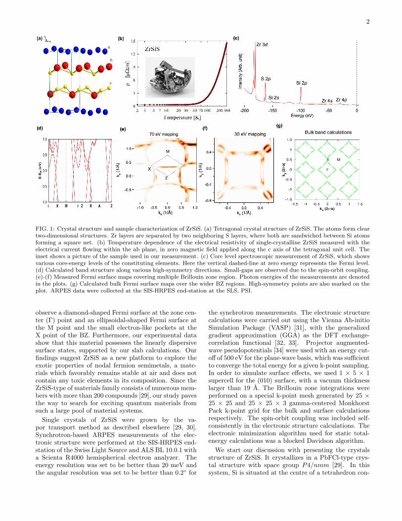
FIG. 1: Crystal structure and sample characterization of ZrSiS. (a) Tetragonal crystal structure of ZrSiS. The atoms form cleartwo-dimensional structures. Zr layers are separated by two neighboring S layers, where both are sandwiched between Si atomsforming a square net. (b) Temperature dependence of the electrical resistivity of single-crystalline ZrSiS measured with theelectrical current flowing within the ab plane, in zero magnetic field applied along the c axis of the tetragonal unit cell. Theinset shows a picture of the sample used in our measurement. (c) Core level spectroscopic measurement of ZrSiS, which showsvarious core-energy levels of the constituting elements. Here the vertical dashed-line at zero energy represents the Fermi level.(d) Calculated band structure along various high-symmetry directions. Small-gaps are observed due to the spin-orbit coupling.(e)-(f) Measured Fermi surface maps covering multiple Brillouin zone region. Photon energies of the measurements are denotedin the plots. (g) Calculated bulk Fermi surface maps over the wider BZ regions. High-symmetry points are also marked on theplot. ARPES data were collected at the SIS-HRPES end-station at the SLS, PSI.
observe a diamond-shaped Fermi surface at the zone cen-ter (Γ) point and an ellipsoidal-shaped Fermi surface atthe M point and the small electron-like pockets at theX point of the BZ. Furthermore, our experimental datashow that this material possesses the linearly dispersivesurface states, supported by our slab calculations. Ourfindings suggest ZrSiS as a new platform to explore theexotic properties of nodal fermion semimetals, a mate-rials which favorably remains stable at air and does notcontain any toxic elements in its composition. Since theZrSiS-type of materials family consists of numerous mem-bers with more than 200 compounds [29], our study pavesthe way to search for exciting quantum materials fromsuch a large pool of material systems.
Single crystals of ZrSiS were grown by the va-por transport method as described elsewhere [29, 30].Synchrotron-based ARPES measurements of the elec-tronic structure were performed at the SIS-HRPES end-station of the Swiss Light Source and ALS BL 10.0.1 witha Scienta R4000 hemispherical electron analyzer. Theenergy resolution was set to be better than 20 meV andthe angular resolution was set to be better than 0.2◦ for
the synchrotron measurements. The electronic structurecalculations were carried out using the Vienna Ab-initioSimulation Package (VASP) [31], with the generalizedgradient approximation (GGA) as the DFT exchange-correlation functional [32, 33]. Projector augmented-wave pseudopotentials [34] were used with an energy cut-off of 500 eV for the plane-wave basis, which was sufficientto converge the total energy for a given k-point sampling.In order to simulate surface effects, we used 1 × 5 × 1supercell for the (010) surface, with a vacuum thicknesslarger than 19 A. The Brillouin zone integrations wereperformed on a special k-point mesh generated by 25 ×25 × 25 and 25 × 25 × 3 gamma-centered MonkhorstPack k-point grid for the bulk and surface calculationsrespectively. The spin-orbit coupling was included self-consistently in the electronic structure calculations. Theelectronic minimization algorithm used for static total-energy calculations was a blocked Davidson algorithm.
We start our discussion with presenting the crystalsstructure of ZrSiS. It crystallizes in a PbFCl-type crys-tal structure with space group P4/nmm [29]. In thissystem, Si is situated at the centre of a tetrahedron con-

3
FIG. 2: Electronic structure measurements of ZrSiS. (a) Fermi surface map (with binding energy of 0 meV shown in the topleft panel) and constant energy contours. The value of the binding energy is denoted at the constant energy contour plots. (b)Dispersion map of ZrSiS along the high-symmetry directions obtained by using incident photon energy of 50 eV at a temperatureof 20 K. ARPES data were collected at the SIS-HRPES end-station at the SLS, PSI. The high-symmetry directions are markedon the plots. (c) Slab calculations along high-symmetry directions. Blue and red curves represent the surface and bulk bands,respectively. Small bulk gap is observed at the X-point along the M-X-M high-symmetry direction.
sisting of Zr atoms (see Fig. 1a). The relatively weakZr-S bonding between two neighboring structures pro-vides a natural cleavage plane between the adjacent ZrSlayers. The crystal easily cleaves along the (001) surface,which contains Zr and S termination. Fig. 1b showsthe temperature dependent resistivity of ZrSiS measuredwithout the applied magnetic field. The zero-field de-pendence resistivity has a clear metallic character withresidual resistivity ratio value (RRR = ρ(300K)/ρ(2K))equal to 50, that confirms the high quality of the crystalused in our measurements. The inset in Fig. 1b showsthe picture of the sample used in our transport and spec-troscopic measurements.
Photoemission spectroscopy (PES) also provides infor-mation about the core level states relative to the chemicalpotential. Figure 1c shows the core levels in the 0 - 200eV binding energy range of the ZrSiS sample. From lowto high binding energies, we observe the Zr 4p (∼ 28 eV),Zr 4s (∼50 eV), Si 2p (∼99 eV), Si 2s (∼ 149 eV), S 2p (∼162 eV) and Zr 3d (∼ 181 eV) states, respectively. Theobservation of the sharp peaks suggests that the sam-
ples used in our spectroscopic measurements are of highquality.
Now we discuss the electronic band structure of theZrSiS system. The calculated bulk band structure alongvarious high-symmetry directions is shown in Fig. 1d.Small-gaps are observed due to the spin-orbit coupling.The measured Fermi surface maps using photon energiesof 70 eV and 30 eV are shown in Fig. 1e and Fig. 1f.These maps are obtained within the energy window of ±5 meV near the Fermi level. Various Fermi pockets areobserved in the Fermi surface map obtained by 70 eV bycovering a larger area of the Brillouin zone. Specifically,a diamond shaped Fermi surface is observed around thezone center (Γ) point, and an ellipsoidal pocket is seenat around the M point. Interestingly, we also observe asmall electron-like Fermi pocket around the X point ofthe BZ. Fig. 1g shows the calculated bulk Fermi surfacemap. By comparing the experimental Fermi surface mapsin Figs. 1e-f with the calculated Fermi surface shown inFig. 1g, it can be concluded that the states around the Xpoint do not originate from the bulk band. We attribute
4
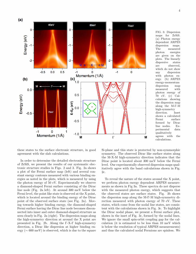
FIG. 3: Dispersionmaps for ZrSiS.(a) Photon energydependent ARPESdispersion maps.The measuredphoton energiesare given on theplots. The linearlydispersive statesare observed,which do not showany dispersionwith photon en-ergy. (b) ARPESenergy-momentumdispersion mapmeasured withphoton energy of70 eV. (c) Cal-culations showingthe dispersion mapalong the M-Γ-Mhigh-symmetrydirection. Insetshows a calculatedFermi surfaceformed by Diracline nodes. Ex-perimental dataqualitativelyagrees with thecalculations.
these states to the surface electronic structure, in goodagreement with the slab calculations.
In order to determine the detailed electronic structureof ZrSiS, we present the results of our systematic elec-tronic structure studies in Figs. 2 and 3. Fig. 2a showsa plot of the Fermi surface map (left) and several con-stant energy contours measured with various binding en-ergies as noted in the plots, which is measured by usingthe photon energy of 50 eV. Experimentally we observea diamond-shaped Fermi surface consisting of the Diracline node (Fig. 2a left). At around 300 meV below theFermi level, the point like state is observed at the X point,which is located around the binding energy of the Diracpoint of the observed surface state (see Fig. 2a). Mov-ing towards higher binding energy, the diamond-shapedFermi surface having the Dirac line node becomes discon-nected into inner and outer diamond-shaped structure asseen clearly in Fig. 2a (right). The dispersion maps alongthe high-symmetry direction at around the X point arepresented in Fig. 2b. Along the Γ-X-Γ high-symmetrydirection, a Dirac like dispersion at higher binding en-ergy (∼ 600 meV) is observed, which is due to the square
Si-plane and this state is protected by non-symmorphicsymmetry. The observed Dirac like surface states alongthe M-X-M high-symmetry direction indicates that theDirac point is located about 300 meV below the Fermilevel. Our experimentally observed dispersion maps qual-itatively agree with the band calculations shown in Fig.2c.
To reveal the nature of the states around the X point,we perform photon energy dependent ARPES measure-ments as shown in Fig 3a. These spectra do not dispersewith the measured photon energy, which suggests thatthe observed states are surface states. Fig. 3b showsthe dispersion map along the M-Γ-M high-symmetry di-rection measured with photon energy of 70 eV. Thesestates, which come from the nodal line states, are consis-tent with the calculations shown in Fig. 3c. To highlightthe Dirac nodal phase, we present a Fermi surface plot,shown in the inset of Fig. 3c, formed by the nodal lines.We ignore the small spin-orbit coupling gap for the cal-culation (it is estimated to be less than 10 meV whichis below the resolution of typical ARPES measurements)and thus the calculated nodal Fermions are spinless. We
5
further note that we do not observe the SOC gap in ex-perimental data, suggesting a negligible size of the SOCgap. To highlight the Dirac nodal phase, we illustrate thenodal lines for a specific plane of the BZ (kz = 0) in theinset of Fig. 3c. Here, the Dirac line nodes connect theDirac points at the Fermi level. Furthermore, we observethat monolayer systems of ZrSiS type materials are in-teresting because these might show edge state protectedby non-symmorphic space group symmetry [12].
In conclusion, we have performed systematic ARPESmeasurements on the ZrSiS system covering a large areaof the Brillouin zone. We reveal the existence of multiple
Fermi pockets and identify their origin, which is com-plemented by our Ab-initio calculations. Importantly,we reveal the existence of the topological spinless nodalsemimetal fermion phase in this system, which emergesbecause of a negligible SOC gap. Our study establishesthe ZrSiS family of materials as a new platform to studythe Dirac line node semimetal phases, with the possibilityof realizing novel exciting quantum phases utilizing thelarge pool of material systems available in this family.
[1] M. Z. Hasan, and C. L. Kane, Colloquium: topologicalinsulators, Rev. Mod. Phys. 82, 3045-3067 (2010).
[2] X.-L. Qi, and S.-C. Zhang, Topological insulators and su-perconductors, Rev. Mod. Phys. 83, 1057 (2011).
[3] Y. Xia, D. Qian, D. Hsieh, L. Wray, A. Pal, H. Lin, A.Bansil, D. Grauer, Y. S. Hor, R. J. Cava, and M. Z.Hasan, Observation of a large-gap topological-insulatorclass with a single Dirac cone on the surface, Nat. Phys.5, 398 (2009).
[4] M. Z. Hasan, S.-Y. Xu, and M. Neupane, TopologicalInsulators: Fundamentals and Perspectives, (John Wileyand Sons, New York, 2015).
[5] Z. Wang, H. Weng, Q. Wu, Xi Dai, and Z. Fang, Three-dimensional Dirac semimetal and quantum transport inCd3As2, Phys. Rev. B 88, 125427 (2013).
[6] M. Neupane, S.-Y. Xu, R. Sankar, N. Alidoust, G. Bian,C. Liu, I. Belopolski, T.-R. Chang, H.-T. Jeng, H. Lin,A. Bansil, F.-C. Chou, and M. Z. Hasan, Observation ofa three-dimensional topological Dirac semimetal phase inhigh-mobility Cd3As2, Nat. Commun. 5, 3786 (2014).
[7] L. Fu, Topological crystalline insulators, Phys. Rev. Lett.106, 106802 (2011).
[8] Q. Xu, Z. Song, S. Nie, H. Weng, Z. Fang, and X. Dai,Two-dimensional oxide topological insulator with iron-pnictide superconductor LiFeAs structure, Phys. Rev.Lett. 106, 106802 (2011).
[9] M. Neupane, N. Alidoust, S.-Y. Xu, T. Kondo, Y. Ishida,D. J. Kim, C. Liu, I. Belopolski, Y. J. Jo, T-R. Chang,H-T. Jeng, T. Durakiewicz, L. Balicas, H. Lin, A. Ban-sil, S. Shin, Z. Fisk, and M. Z. Hasan, Surface elec-tronic structure of the topological Kondo-insulator can-didate correlated electron system SmB6, Nat. Commun.4, 2991 (2013).
[10] B.-J. Yang, and N. Nagaosa, Classification of stable three-dimensional Dirac semimetals with nontrivial topology,Nat. Commun. 5, 4898 (2014).
[11] M. Neupane, S.-Y. Xu, N. Alidoust, G. Bian, D. J.Kim, C. Liu, I. Belopolski, T.-R. Chang, H.-T. Jeng,T. Durakiewicz, H. Lin, A. Bansil, Z. Fisk, and M. Z.Hasan, Non-Kondo-like Electronic Structure in the Cor-related Rare-Earth Hexaboride YbB6, Phys. Rev. Lett.114, 016403 (2015).
[12] S. M. Young and C. L. Kane, Dirac Semimetals in TwoDimensions, Phys. Rev. Lett. 115, 126803 (2015).
[13] S.-M. Huang, S.-Y. Xu, I. Belopolski, C.-C. Lee, G.Chang, B. Wang, N. Alidoust, G. Bian, M. Neupane,
C. Zhang, S. Jia, A. Bansil, H. Lin, and M. Z. Hasan,A Weyl Fermion semimetal with surface Fermi arcs inthe transition metal monopnictide TaAs class, Nat. Com-mun. 6, 7373 (2015).
[14] H. Weng, C. Fang, Z. Fang, B. A. Bernevig, andX. Dai, Weyl Semimetal Phase in Noncentrosymmet-ric Transition-Metal Monophosphides, Phys. Rev. X 5,011029 (2015).
[15] S.-Y. Xu, I. Belopolski, N. Alidoust, M. Neupane, G.Bian, C. Zhang, R. Sankar, G. Chang, Z. Yuan, C.- C.Lee, S.-M. Huang, H. Zheng, J. Ma, D. S. Sanchez, B.Wang, A. Bansil, F. Chou, P. P. Shibayev, H. Lin, S. Jia,and M. Z. Hasan, Discovery of a Weyl fermion semimetaland topological Fermi arcs, Science 349, 613 (2015).
[16] B. Q. Lv, H. M. Weng, B. B. Fu, X. P. Wang, H. Miao, J.Ma, P. Richard, X. C. Huang, L. X. Zhao, G. F. Chen, Z.Fang, X. Dai, T. Qian, and H. Ding, Experimental Dis-covery of Weyl Semimetal TaAs, Phys. Rev. X 5, 031013(2015).
[17] I. Belopolski, S.-Y. Xu, D. S. Sanchez, G. Chang, C.Guo, M. Neupane, H. Zheng, C.-C. Lee, S.-M. Huang,G. Bian, N. Alidoust, T.-R. Chang, B. Wang, X. Zhang,A. Bansil, H.-T. Jeng, H. Lin, S. Jia, and M. Z. Hasan,Criteria for Directly Detecting Topological Fermi Arcs inWeyl Semimetals, Phys. Rev. Lett. 116, 066802 (2016).
[18] M. Z. Hasan, S.-Y. Xu and G. Bian, Topological in-sulators, topological superconductors and Weyl fermionsemimetals: discoveries, perspectives and outlooks, Phys.Scr. T164, 014001 (2015).
[19] A. A. Burkov, M. D. Hook, and L. Balents. Topologicalnodal semimetals, Phys. Rev. B 84, 235126 (2011)
[20] M. Phillips and V. Aji, Tunable line node semimetals,Phys. Rev. B 90, 115111 (2014).
[21] H. Weng, Y. Liang, Q. Xu, R. Yu, Z. Fang, X. Dai, andY. Kawazoe, Topological node-line semimetal in three-dimensional graphene networks, Phys. Rev. B 92, 045108(2015).
[22] Y. Kim, B. J. Wieder, C. L. Kane, and A. M.Rappe, Dirac Line Nodes in Inversion-Symmetric Crys-tals, Phys. Rev. Lett. 115, 036806 (2015).
[23] L. S. Xie, L. M. Schoop, E. M. Seibel, Q. D. Gibson, W.Xie, and R. J. Cava, A new form of Ca3P2 with a ringof Dirac nodes, Appl. Phys. Lett. Mat. 3, 083602 (2015).
[24] X. Wan, A. M. Turner, A. Vishwanath, and S. Y.Savrasov, Topological semimetal and Fermi-arc surfacestates in the electronic structure of pyrochlore iridates,
6
Phys. Rev. B 83, 205101 (2011).[25] A. A. Burkov and L. Balents, Weyl Semimetal in a Topo-
logical Insulator Multilayer, Phys. Rev. Lett. 107, 127205(2011).
[26] G. Xu, H. Weng, Z. Wang, Xi Dai, and Z. Fang, ChernSemimetal and the Quantized Anomalous Hall Effect inHgCr2Se4, Phys. Rev. Lett. 107, 186806 (2011).
[27] G. Bian, T.-R. Chang, R. Sankar, S.-Y. Xu, H. Zheng,T. Neupert, C.-K. Chiu, S.-M. Huang, G. Chang, I. Be-lopolski, D. S. Sanchez, M. Neupane, N. Alidoust, C. Liu,B. Wang, C.-C. Lee, H.-T. Jeng, C. Zhang, Z. Yuan, S.Jia, A. Bansil, F. Chou, H. Lin, and M. Z. Hasan, Topo-logical nodal-line fermions in spin-orbit metal PbTaSe2,Nat. Commun. 7, 10556 (2016).
[28] L. M. Schoop, M. N. Ali, C. Straber, V. Duppel, S. S. P.Parkin, B. V. Lotsch, and C. R. Ast, Dirac Cone Pro-tected by Non-Symmorphic Symmetry and 3D Dirac LineNode in ZrSiS, arXiv:1509.00861v1 (2015).
[29] C. Wang, and T. Hughbanks, Main Group Element Sizeand Substitution Effects on the Structural Dimensionalityof Zirconium Tellurides of the ZrSiS Type, Inorg. Chem.34, 5524-5529 (1995).
[30] R. Singha, A. Pariari, B. Satpati, and P. Mandal, Titanicmagnetoresistance and signature of non-degenerate Diracnodes in ZrSiS, arXiv:1602.01993v1 (2016).
[31] G. Kresse, and J. Furthmuller, Efficient iterative schemesfor ab initio total-energy calculations using a plane-wavebasis set, Phys. Rev. B. 54, 11169 (1996).
[32] G. Kresse, and D. Joubert, From ultrasoft pseudopoten-tials to the projector augmented-wave method, Phys. Rev.B 59, 1758 (1999).
[33] J. P. Perdew, K. Burke, and M. Ernzerhof, GeneralizedGradient Approximation Made Simple, Phys. Rev. Lett.
77, 3865 (1996).[34] G. Kresse, and J. Hafner, Ab initio molecular dynamics
for open-shell transition metals, Phys. Rev. B 48, 13115(1993).
Acknowledgements
M.N. is supported by the start-up fund from theUniversity of Central Florida. T.D. is supported byNSF IR/D program. I. B. acknowledges the supportof the NSF GRFP. D.K. was supported by the Na-tional Science Centre (Poland) under research grant2015/18/A/ST3/00057. Work at Princeton Universityis supported by the Emergent Phenomena in QuantumSystems Initiative of the Gordon and Betty Moore Foun-dation under Grant No. GBMF4547 (M.Z.H.) and by theNational Science Foundation, Division of Materials Re-search, under Grants No. NSF-DMR-1507585 and No.NSF-DMR-1006492. P.M. and P.M.O. acknowledge sup-port from the Swedish Research Council (VR), the K.and A. Wallenberg Foundation and the Swedish NationalInfrastructure for computing (SNIC). We thank PlumbNicholas Clark for beamline assistance at the SLS, PSI.We also thank Sung-Kwan Mo for beamline assistance atthe LBNL.
Correspondence and requests for materials should beaddressed to M.N. (Email: [email protected]).