npn silicon rf transistor ne85634 / 2sc3357 data sheet pu10211ej01v0ds ne85634 / 2sc3357 thermal...
TRANSCRIPT
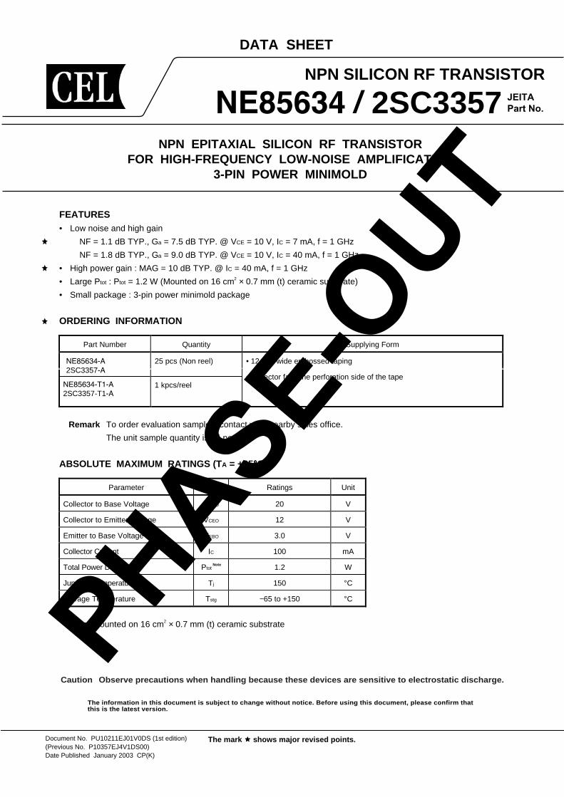
DATA SHEET
Caution Observe precautions when handling because these devices are sensitive to electrostatic discharge.
The information in this document is subject to change without notice. Before using this document, please confirm that this is the latest version.
NPN SILICON RF TRANSISTOR
NE85634 / 2SC3357NPN EPITAXIAL SILICON RF TRANSISTOR
FOR HIGH-FREQUENCY LOW-NOISE AMPLIFICATION3-PIN POWER MINIMOLD
Document No. PU10211EJ01V0DS (1st edition)(Previous No. P10357EJ4V1DS00)Date Published January 2003 CP(K)
The mark ���� shows major revised points.
FEATURES• Low noise and high gain
NF = 1.1 dB TYP., Ga = 7.5 dB TYP. @ VCE = 10 V, IC = 7 mA, f = 1 GHz
NF = 1.8 dB TYP., Ga = 9.0 dB TYP. @ VCE = 10 V, IC = 40 mA, f = 1 GHz
• High power gain : MAG = 10 dB TYP. @ IC = 40 mA, f = 1 GHz
• Large Ptot : Ptot = 1.2 W (Mounted on 16 cm2 × 0.7 mm (t) ceramic substrate)
• Small package : 3-pin power minimold package
ORDERING INFORMATION
Part Number Quantity Supplying Form
NE85634-A2SC3357-A
25 pcs (Non reel) • 12 mm wide embossed taping
NE85634-T1-A2SC3357-T1-A
1 kpcs/reel• Collector face the perforation side of the tape
Remark To order evaluation samples, contact your nearby sales office.
The unit sample quantity is 25 pcs.
ABSOLUTE MAXIMUM RATINGS (T A = +25°°°°C)
Parameter Symbol Ratings Unit
Collector to Base Voltage VCBO 20 V
Collector to Emitter Voltage VCEO 12 V
Emitter to Base Voltage VEBO 3.0 V
Collector Current IC 100 mA
Total Power Dissipation Ptot Note 1.2 W
Junction Temperature Tj 150 °C
Storage Temperature Tstg −65 to +150 °C
Note Mounted on 16 cm2 × 0.7 mm (t) ceramic substrate
JEITAPart No.
PHASE-OUT
Data Sheet PU10211EJ01V0DS2
NE85634 / 2SC3357
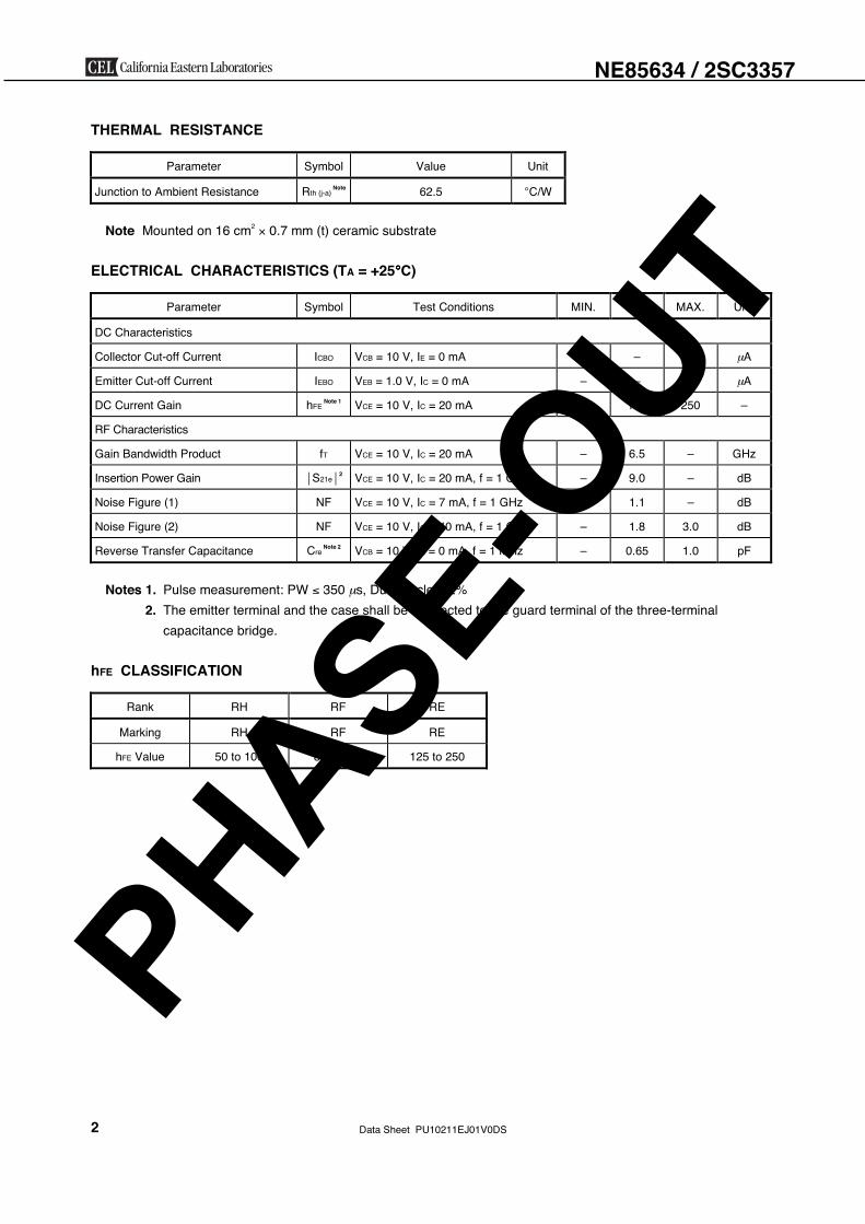
THERMAL RESISTANCE
Parameter Symbol Value Unit
Junction to Ambient Resistance Rth (j-a)Note 62.5 °C/W
Note Mounted on 16 cm2 × 0.7 mm (t) ceramic substrate
ELECTRICAL CHARACTERISTICS (TA = +25°°°°C)
Parameter Symbol Test Conditions MIN. TYP. MAX. Unit
DC Characteristics
Collector Cut-off Current ICBO VCB = 10 V, IE = 0 mA – – 1.0 μA
Emitter Cut-off Current IEBO VEB = 1.0 V, IC = 0 mA – – 1.0 μA
DC Current Gain hFE Note 1 VCE = 10 V, IC = 20 mA 50 120 250 –
RF Characteristics
Gain Bandwidth Product fT VCE = 10 V, IC = 20 mA – 6.5 – GHz
Insertion Power Gain ⏐S21e⏐2 VCE = 10 V, IC = 20 mA, f = 1 GHz – 9.0 – dB
VFN)1( erugiF esioN CE = 10 V, IC = 7 mA, f = 1 GHz – 1.1 – dB
VFN)2( erugiF esioN CE = 10 V, IC = 40 mA, f = 1 GHz – 1.8 3.0 dB
Reverse Transfer Capacitance CreNote 2 VCB = 10 V, IE = 0 mA, f = 1 MHz – 0.65 1.0 pF
Notes 1. Pulse measurement: PW ≤ 350 μs, Duty Cycle ≤ 2%2. The emitter terminal and the case shall be connected to the guard terminal of the three-terminal
capacitance bridge.
hFE CLASSIFICATION
Rank RH RF RE
Marking RH RF RE
hFE Value 50 to 100 80 to 160 125 to 250
PHASE-OUT

Data Sheet PU10211EJ01V0DS 3
TYPICAL CHARACTERISTICS (TA = +25°°°°C, unless otherwise specified)D
C C
urre
nt G
ain
hFE
Collector Current IC (mA)
DC CURRENT GAIN vs.COLLECTOR CURRENT
200
50
100
10
20
1 5 10 055.0
VCE = 10 V
2
1
0 25 50 75 100 125 150
Tota
l Pow
er D
issi
patio
n P
tot (
W)
Ambient Temperature TA (˚C)
TOTAL POWER DISSIPATIONvs. AMBIENT TEMPERATURE
Ceramic substrate16 cm2 × 0.7 mm (t)
Free air Rth (j-a) 312.5˚C/W
Rev
erse
Tra
nsfe
r Cap
acita
nce
Cre (p
F)
Collector to Base Voltage VCB (V)
REVERSE TRANSFER CAPACITANCEvs. COLLECTOR TO BASE VOLTAGE2
1
0.5
0.30.50.2 1 2 5 10 3020
f = 1 MHz
VCE = 10 V
Gai
n Ba
ndw
idth
Pro
duct
fT (
GH
z)
Collector Current IC (mA)
GAIN BANDWIDTH PRODUCTvs. COLLECTOR CURRENT
10
32
5
0.20.3
0.5
1
0.11 5 10 50 0015.01.0
VCE = 10 Vf = 1 GHz
Collector Current IC (mA)
INSERTION POWER GAINvs. COLLECTOR CURRENT
Inse
rtion
Pow
er G
ain
|S21
e|2 (dB)
15
10
0
5
0.5 1 10 50 075
VCE = 10 VIC = 20 mA
Frequency f (GHz)
INSERTION POWER GAIN, MAGvs. FREQUENCY
Inse
rtion
Pow
er G
ain
|S21
e|2 (dB)
Max
imum
Ava
ilabl
e Po
wer
Gai
n M
AG (d
B) 25
15
20
5
10
00.05 0.1 0.5 1 22.0
MAG
|S21e|2
NE85634 / 2SC3357
PHASE-OUT
Data Sheet PU10211EJ01V0DS4
90
100
80
70
60
40
50
3020 30 40 50 60 70
Collector Current IC (mA)
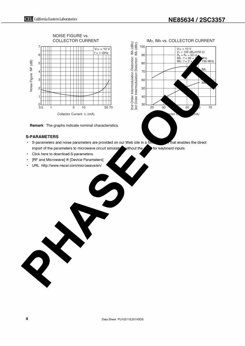
IM2, IM3 vs. COLLECTOR CURRENT
2nd
Ord
er In
term
odul
atio
n D
isto
rtion
IM
2 (dB
c)3r
d O
rder
Inte
rmod
ulat
ion
Dis
torti
on I
M3 (
dBc)
IM2
IM3
VCE = 10 VVo = 100 dB V/50 ΩRg = Re = 50 ΩIM2 : f = 90 + 100 MHzIM3 : f = 2 × 200 – 190 MHz
μ
7
0
1
2
3
4
5
6
0.5 1 5 10 50 70
Collector Current IC (mA)
NOISE FIGURE vs. COLLECTOR CURRENT
Noi
se F
igur
e N
F (d
B)
VCE = 10 Vf = 1 GHz
Remark The graphs indicate nominal characteristics.
S-PARAMETERS
NE85634 / 2SC3357
PHASE-OUT
Data Sheet PU10211EJ01V0DS 5
SMITH CHART
S21e-FREQUENCYCONDITION : VCE = 10 V, IC = 20 mA
90˚
0˚
30˚
–30˚
60˚
–60˚
180˚
150˚
–150˚
120˚
–120˚–90˚
3 6 9 12 15
S21e
f = 0.2 GHz
f = 2.0 GHz
S12e-FREQUENCYCONDITION : VCE = 10 V, IC = 20 mA
90˚
0˚
30˚
–30˚
60˚
–60˚
180˚
150˚
–150˚
120˚
–120˚–90˚
0.1 0.2 0.3 0.4 0.5
S12e
f = 0.2 GHz
f = 2.0 GHz
S11e, S22e-FREQUENCYCONDITION : VCE = 10 V
60
20
30
40
50
708090100
110
120
130
140
150
−160
−150
−140
−130
−120
−110−100 −90 −80
−70
−60
−50
−40
−30
−20−10
010
0.22
0.20
0.18
0.16
0.140.120.10
0.08
0.06
0.04
0.21
0.19
0.17
0.150.130.11
0.09
0.07
0.05
0.03
0.02
0.01
00.
490.
480.
47
0.46
0.45
0.44
0.43
0.42
0.41
0.400.39 0.38 0.37 0.36
0.35
0.34
0.33
0.32
0.31
0.30
0.29
0.280.27
0.2652
.00.24
0.23
0.28
0.30
0.32
0.34
0.360.380.40
0.42
0.44
0.46
0.29
0.31
0.33
0.350.370.39
0.41
0.43
0.45
0.47
0.48
0.49
00.
010.
020.
03
0.04
0.05
0.06
0.07
0.08
0.09
0.100.11 0.12 0.13 0.14
0.15
0.16
0.17
0.18
0.19
0.20
0.21
0.220.23
0.2452
.00.26
0.27W
AVEL
ENG
THS
TOW
ARD
LOAD
ANG
LEO
FRE
FLEC
TIO
NCO
EFFC
IENT
INDE
GRE
ES
WAV
ELEN
GTH
STO
WAR
DGE
NERA
TOR
REACTANCE COMPONENT
( R –––– ZO )
( +JX
–––
–
ZO
)
POSIT
IVE R
EACT
ANCE
COMPONENT
NEGATIVEREA
CTAN
CE CO
MPO
NENT
(−JX
–––
–
Z
O)
0.80.
7
0.6
0.3
0.2
0.1
0.4
0.5
5.0
10
50
3.0
4.0
1.8
2.0
1.20.10.9 1.
4
1.6
20
2.0
50
10
6.0
4.0
3.0
1.8
1.61.
41.20.9
0.8
0.7
0.6
0.5
0.4
0.3
0.2
0.1
0.1
20
0.2
0.4
0.6
0.8
1.0
0.2
0.4
0.6
0.8
1.0
0.2
1.0
0.8
0.6
0.4
1.0
0.8
0.6
0.2
0.4
0.1
0.2
0.3
0.4
0.5
0.6
0.7
0.8
0.9
1.0
1.4
1.6
1.8
2.0
3.0
4.0
5.0 10 200 1.2
f = 0.2 GHzf = 0.2 GHz
f = 2.0 GHz
f = 20 GHzS11e
S22e
: IC = 20 mA: IC = 40 mA
NE85634 / 2SC3357
PHASE-OUT
Data Sheet PU10211EJ01V0DS6
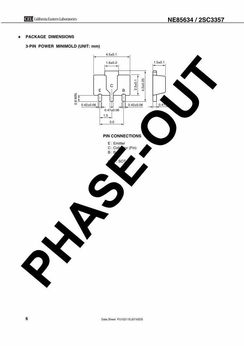
PACKAGE DIMENSIONS
3-PIN POWER MINIMOLD (UNIT: mm)
1.5±0.1
0.41+0.03–0.06
4.5±0.1
0.42±0.060.42±0.06
1.6±0.2
3.0
1.5
CE B 2.
5±0.
1
4.0±
0.25
0.8
MIN
.
0.47±0.06
E : EmitterC : Collector (Fin)B : Base
(IEC : SOT-89)
PIN CONNECTIONS
NE85634 / 2SC3357
PHASE-OUT

NOTICE
1. Descriptions of circuits, software and other related information in this document are provided only to illustrate the operation of semiconductor products and application examples. You are fully responsible for the incorporation of these circuits, software, and information in the design of your equipment. California Eastern Laboratories and Renesas Electronics assumes no responsibility for any losses incurred by you or third parties arising from the use of these circuits, software, or information.
2. California Eastern Laboratories has used reasonable care in preparing the information included in this document, but California Eastern Laboratories does not warrant that such information is error free. California Eastern Laboratories and Renesas Electronics assumes no liability whatsoever for any damages incurred by you resulting from errors in or omissions from the information included herein.
3. California Eastern Laboratories and Renesas Electronics do not assume any liability for infringement of patents, copyrights, or other intellectual property rights of third parties by or arising from the use of Renesas Electronics products or technical information described in this document. No license, express, implied or otherwise, is granted hereby under any patents, copyrights or other intellectual property rights of California Eastern Laboratories or Renesas Electronics or others.
4. You should not alter, modify, copy, or otherwise misappropriate any Renesas Electronics product, whether in whole or in part. California Eastern Laboratories and Renesas Electronics assume no responsibility for any losses incurred by you or third parties arising from such alteration, modification, copy or otherwise misappropriation of Renesas Electronics product.
5. Renesas Electronics products are classified according to the following two quality grades: “Standard” and “High Quality”. The recommended applications for each Renesas Electronics product depends on the product’s quality grade, as indicated below. “Standard”: Computers; office equipment; communications equipment; test and measurement equipment; audio and visual equipment; home electronic appliances; machine tools; personal electronic equipment; and industrial robots etc. “High Quality”: Transportation equipment (automobiles, trains, ships, etc.); traffic control systems; anti-disaster systems; anti-crime systems; and safety equipment etc. Renesas Electronics products are neither intended nor authorized for use in products or systems that may pose a direct threat to human life or bodily injury (artificial life support devices or systems, surgical implantations etc.), or may cause serious property damages (nuclear reactor control systems, military equipment etc.). You must check the quality grade of each Renesas Electronics product before using it in a particular application. You may not use any Renesas Electronics product for any application for which it is not intended. California Eastern Laboratories and Renesas Electronics shall not be in any way liable for any damages or losses incurred by you or third parties arising from the use of any Renesas Electronics product for which the product is not intended by California Eastern Laboratories or Renesas Electronics.
6. You should use the Renesas Electronics products described in this document within the range specified by California Eastern Laboratories, especially with respect to the maximum rating, operating supply voltage range, movement power voltage range, heat radiation characteristics, installation and other product characteristics. California Eastern Laboratories shall have no liability for malfunctions or damages arising out of the use of Renesas Electronics products beyond such specified ranges.
7. Although Renesas Electronics endeavors to improve the quality and reliability of its products, semiconductor products have specific characteristics such as the occurrence of failure at a certain rate and malfunctions under certain use conditions. Further, Renesas Electronics products are not subject to radiation resistance design. Please be sure to implement safety measures to guard them against the possibility of physical injury, and injury or damage caused by fire in the event of the failure of a Renesas Electronics product, such as safety design for hardware and software including but not limited to redundancy, fire control and malfunction prevention, appropriate treatment for aging degradation or any other appropriate measures. Because the evaluation of microcomputer software alone is very difficult, please evaluate the safety of the final products or systems manufactured by you.
8. Please contact a California Eastern Laboratories sales office for details as to environmental matters such as the environmental compatibility of each Renesas Electronics product. Please use Renesas Electronics products in compliance with all applicable laws and regulations that regulate the inclusion or use of controlled substances, including without limitation, the EU RoHS Directive. California Eastern Laboratories and Renesas Electronics assume no liability for damages or losses occurring as a result of your noncompliance with applicable laws and regulations.
9. Renesas Electronics products and technology may not be used for or incorporated into any products or systems whose manufacture, use, or sale is prohibited under any applicable domestic or foreign laws or regulations. You should not use Renesas Electronics products or technology described in this document for any purpose relating to military applications or use by the military, including but not limited to the development of weapons of mass destruction. When exporting the Renesas Electronics products or technology described in this document, you should comply with the applicable export control laws and regulations and follow the procedures required by such laws and regulations.
10. It is the responsibility of the buyer or distributor of California Eastern Laboratories, who distributes, disposes of, or otherwise places the Renesas Electronics product with a third party, to notify such third party in advance of the contents and conditions set forth in this document, California Eastern Laboratories and Renesas Electronics assume no responsibility for any losses incurred by you or third parties as a result of unauthorized use of Renesas Electronics products.
11. This document may not be reproduced or duplicated in any form, in whole or in part, without prior written consent of California Eastern Laboratories.12. Please contact a California Eastern Laboratories sales office if you have any questions regarding the information contained in this document or Renesas
Electronics products, or if you have any other inquiries.
NOTE 1: “Renesas Electronics” as used in this document means Renesas Electronics Corporation and also includes its majority-owned subsidiaries.NOTE 2: “Renesas Electronics product(s)” means any product developed or manufactured by or for Renesas Electronics.NOTE 3: Products and product information are subject to change without notice.
CEL Headquarters • 4590 Patrick Henry Drive, Santa Clara, CA 95054 • Phone (408) 919-2500 • www.cel.com
For a complete list of sales offices, representatives and distributors,Please visit our website: www.cel.com/contactusPHASE-O
UT