novel three-phase cm/dm conducted emission separator · pdf fileieee transactions on...
TRANSCRIPT

Novel Three-Phase CM/DM Conducted Emission Separator
Marcelo Lobo Heldwein, Member, IEEE, Jürgen Biela, Member, IEEE, Hans Ertl, Member, IEEE,
Thomas Nussbaumer, Member, IEEE, and Johann W. Kolar, Senior Member, IEEE „This material is posted here with permission of the IEEE. Such permission of the IEEE does not in any way imply IEEE endorsement of any of ETH Zürich’s products or services. Internal or personal use of this material is permitted. However, permission to reprint/republish this material for advertising or promo-tional purposes or for creating new collective works for resale or redistribution must be obtained from the IEEE by writing to [email protected]. By choosing to view this document you agree to all provisions of the copyright laws protecting it.”

IEEE TRANSACTIONS ON INDUSTRIAL ELECTRONICS, VOL. 56, NO. 9, SEPTEMBER 2009 3693
Novel Three-Phase CM/DM ConductedEmission Separator
Marcelo Lobo Heldwein, Member, IEEE, Jürgen Biela, Member, IEEE, Hans Ertl, Member, IEEE,Thomas Nussbaumer, Member, IEEE, and Johann W. Kolar, Senior Member, IEEE
Abstract—This paper presents two novel three-phase common-mode (CM)/differential-mode (DM) noise separation networks,which are passive and active networks, to be used in electro-magnetic compatibility conducted emission (CE) measurements ofthree-phase equipment. The passive network is analyzed theoret-ically, and a prototype is constructed and tested. Its evaluationis presented through frequency response measurements and CEtests performed on a three-phase motor drive and verifies that thenetwork is capable of separating the CM and DM information ina CE measurement condition.
Index Terms—Conducted emissions (CEs), electromagneticcompatibility (EMC) measurements, EMC test setup, noiseseparator.
I. INTRODUCTION
THREE-PHASE conducted emission (CE) measurementsare a major issue for developing high-power electronic
equipment that is connected to an electric power grid due toelectromagnetic compatibility (EMC) concerns which are re-flected in international and regional product regulations. Three-phase power electronic systems, such as motor drives and highpower rectifiers, must comply with these regulations. To achieveEMC compliance, electronic equipment must include filteringand/or other electromagnetic emission control strategies.
The development and dimensioning of these emission controltechniques are being increasingly investigated, and as a result,analytical, such as presented in [1]–[5], and experimental toolsare being developed to support the electrical design engineers.There, the qualitative and quantitative assessment of the noisemodes—common mode (CM) or differential mode (DM)—is ofgreat importance since they significantly influence the emissioncontrol strategy (e.g., CM or DM filter). Therefore, a device thatcan be integrated in a three-phase CE standard measurementsystem and that enables the separate evaluation of CM and DMemission levels is presented in this paper. This device is calledthree-phase CM/DM noise separator in the following.
Manuscript received November 24, 2008; revised May 29, 2009. Firstpublished June 16, 2009; current version published August 12, 2009
M. L. Heldwein is with the Power Electronics Institute, Federal Univer-sity of Santa Catarina, Florianópolis 88040-970, Brazil (e-mail: [email protected]).
J. Biela and J. W. Kolar are with the Electrical Engineering Depart-ment, Swiss Federal Institute of Technology (ETH), 8092 Zürich, Switzerland(e-mail: [email protected]; [email protected]).
H. Ertl is with the Research and Technology Department, Technische Uni-versität Wien, 1040 Vienna, Austria (e-mail: [email protected]).
T. Nussbaumer is with Levitronix GmbH, 8005 Zürich, Switzerland(e-mail: [email protected]).
Color versions of one or more of the figures in this paper are available onlineat http://ieeexplore.ieee.org.
Digital Object Identifier 10.1109/TIE.2009.2025287
Circuits enabling the distinction of noise modes for single-phase systems have been presented in [3]–[13], and theiroperating principle is based on the fact that summing andsubtracting of two sensed voltages directly lead to CM and/orDM emissions. Other methods that apply mathematical analysisthrough fast Fourier transformation [14] have also been pro-posed. There, it is important that sampling rates are high enoughand phase information is computed correctly, which usuallyleads to expensive or inaccurate measurements.
A three-phase measurement system capable of separatelymeasuring both noise modes is proposed in [15]. It employscurrent transducers and hybrid junctions [15]. However, thissystem does not fulfill all the specifications of CISPR 16, and itrequires a complex assembly for the test setup. In [14], anothermeasurement technique is presented, which is suitable for highpower levels, but it does not use a line impedance stabilizationnetwork (LISN) and needs numerical treatment for the acquireddata. Numerical models are presented in [16], which also allowCM and DM emission level estimation but only if a detailedmodel of the system is available. Another method is givenin [17], which uses postmathematical processing in order tocalculate the CM/DM emission values based on the noise prop-agation characteristics for the converter under consideration.
In order to overcome the mentioned limitations, a novelmeasurement hardware, which is inserted between the three-phase LISN and the EMC test receiver, is proposed in this paper.This hardware enables a real-time direct measurement of DMand CM emission levels in a typical CISPR 16 specified setup[18]–[20].
In Section II, a short discussion on CE measurements inthree-phase systems and the mathematical relationships be-tween measured voltages and noise modes are presented.This provides the analytical basis for the CM/DM separa-tion in three-phase systems. Two basic circuit topologies forthree-phase CM/DM separation networks—passive- and active-component-based ones—are proposed in Section III. There,only the passive topology is analyzed in detail for the sakeof brevity. Details of the active circuit can be found in [21].A hardware realization of the passive circuit is discussed inSection IV, and experimental results, illustrating the perfor-mance of the hardware prototype, are given in Section V.
II. REVIEW OF THREE-PHASE CE MEASUREMENTS
AND NOISE COMPONENTS
In order to obtain noise measurements, which are comparableto measurements under different line conditions and which
0278-0046/$26.00 © 2009 IEEE

3694 IEEE TRANSACTIONS ON INDUSTRIAL ELECTRONICS, VOL. 56, NO. 9, SEPTEMBER 2009
Fig. 1. Typical three-phase CE compliant measurement setup schematic and HF equivalent circuit.
comply to CE standards, an LISN has to be utilized. There,the LISN basically has to fulfill the following three functions:1) Define the mains impedance in order to standardize themeasurement; 2) decouple the low frequency ac power supplyvoltage from the measurement equipment; and 3) provide a highfrequency (HF) coupling path between the equipment under test(EUT) and the measurement test receiver.
The impedance curve of an LISN is defined in the EMCstandards, for instance, in CISPR 16 [20]. A typical realizationof a three-phase LISN circuit is shown in Fig. 1 along with asimplified HF equivalent circuit (cf. Fig. 1). For the CE mea-surement process, a test receiver with 50-Ω input impedanceis connected to one of the LISN channels while the remainingtwo LISN ports are terminated with a 50-Ω resistor providing asymmetric measurement condition.
Assuming an ideal decoupling of the EUT from the mainsand a perfect coupling to the test receiver at high frequencies(> 150 kHz), the circuit shown in Fig. 1 could be simplifiedto the HF equivalent circuit shown in the left side of Fig. 1.There, the input ports a, b, and c of the EUT are directlyconnected to the input ports of the test receiver and all HFnoises from the EUT are directly coupled to the test receiver,while the mains ports A, B, and C are separated from the EUT.
The measured voltages ui (i = a, b, c) at the test receiver50-Ω sensing resistors (cf. Fig. 1) consist of DM and CMcomponents
ui = uDM,i + uCM. (1)
These two components are caused by the three DM currentsiDM,i and a CM current iCM circulating between the EUTand the test receiver. There, the currents ii, flowing to the testreceiver input ports, are given by
ii = iDM,i +iCM
3. (2)
Furthermore, the sum of the DM currents is, per definition,equal to zero, and the sum of the currents flowing to the testreceiver is equal to the CM current
ia + ib + ic = iCM. (3)
Therefore, the CM voltage uCM can be evaluated by thesummation of the measured voltages
ua + ub + uc = R · (ia + ib + ic) = R · iCM = 3 · uCM (4)
where R is the input resistance of the test receiver (typically50 Ω). For calculating the DM components, the CM part hasto be eliminated. This can be achieved by subtracting two testreceiver voltages
ua − ub = uDM,a − uDM,b (5)
since ui = uDM,i + uCM/3.Based on (4) and (5), it is now possible to evaluate the
CM and DM components separately, as will be shown in thefollowing section.
III. THREE-PHASE NOISE SEPARATION NETWORKS
In order to practically implement the mathematical formula-tion given in the previous section and properly separate bothnoise modes, two circuit topologies are proposed in Fig. 2 [21].There, the HF noise components are depicted by a CM voltagesource uCM and three DM voltage sources uDM,a, uDM,b,and uDM,c.
In Fig. 2(a), a purely passive solution with three transformersin Y/Δ-connection is shown, which will be analyzed in detailas follows. The active circuit given in Fig. 2(b) builds the CMvoltage by adding all three input voltages and dividing thesum by three (4). Then, the DM voltage could be calculatedby subtracting the CM voltage from the measured voltageby using operational amplifiers. In order to obtain good HFresults, amplifiers with very large bandwidths and high powersupply rejection ratios are required. Furthermore, the active so-lution requires a galvanically insulated power supply with lowcapacitive coupling to ground/mains, which increases costs.However, the active solution would provide well-defined inputimpedances and a good control of the insertion loss, allowingan easy compensation.
Because of the mentioned disadvantages of the active solu-tion and the simplicity of the passive one, the focus is put on the

HELDWEIN et al.: NOVEL THREE-PHASE CM/DM CONDUCTED EMISSION SEPARATOR 3695
Fig. 2. Three-phase CM/DM noise separator proposals [21]. (a) Passivesolution. (b) Active solution.
passive solution in the following. Further details on an activeseparator can be found in [21].
In the next step, the ideal passive separator is analyzedtheoretically, and thereafter, the influence of parasitic elementsof the passive components is investigated.
A. Analysis of the Passive Noise Separator
The passive solution shown in Fig. 2(a) mainly consistsof three transformers Tra, Trb, and Trc with star-connectedprimaries, delta-connected secondary windings, and a one-to-one turns ratio. The primary side star point is connected to theground via a resistor R/3, while the secondary windings areterminated by resistors with the value R.
The CM voltage is built by adding the three currents com-ing from the EUT (4). Due to the Y/Δ-connection of thetransformers, the CM current on the primary side, which isequal in all three transformers/phases, flows on the secondaryside in the triangle of the Δ-connection and not via the DMresistors (cf. Fig. 3(a) and Fig. 5). Therefore, the CM cur-rent does not cause a voltage drop on the secondary side(the Δ-connection acts like a short circuit in the zero se-quence system), and only the DM current, which must flowvia the resistors on the secondary side, causes a voltage drop[cf. Fig. 3(b)].
This behavior also could be determined by mathematical anal-ysis of the circuit, which will be explained in the following for
Fig. 3. Simplified equivalent circuits of the noise separator shown in Fig. 2(a)for (a) CM and (b) DM in the case of symmetric components/design (i.e.,uDM,a + uDM,b + uDM,c = 0 → ia + ib + ic = 0).
further clarifying the noise separation. First, the mesh equation
uCM + uDM,i − uDM,out,i = uCM,out (6)
is set up [cf. Fig. 2(a)]. There, the DM output voltage uDM,out,i
has been transferred to the primary. Due to the Δ-connectionon the secondary side, the sum of the DM voltages at the outputmust be zero
3∑i−1
uDM,out,i = 0. (7)
Furthermore, the sum of the DM voltage sources uDM,i mustbe zero due to their definition
3∑i−1
uDM,i = 0. (8)
This leads to
uCM = uCM,out (9)
which results by summing the three equations (6) (i = a, b, c),inserting (7) and (8), and dividing the result by three.
With (9), the CM voltage UCM,out in (6) could be replacedby uCM. This results in
uDM,i = uDM,out,i. (10)
Therefore, the proposed network perfectly separates the CMand DM voltages and provides in its output ports the values forthe respective voltages if parasitic elements are neglected.

3696 IEEE TRANSACTIONS ON INDUSTRIAL ELECTRONICS, VOL. 56, NO. 9, SEPTEMBER 2009
Fig. 4. Circuit used for the calculation of the input impedances toground (PE).
B. Input Impedance Calculation
Another relevant issue for the measurement setup is thevalue of the input impedances of the network, since the CEmeasurements with an LISN usually specify 50-Ω balancedsensing resistors. Since the network is symmetric, the analysisof the input impedances is performed only for input a, as shownin Fig. 4.
Solving the mesh and node equations for the circuit given inFig. 4 leads to
ua
ia= 9 · Ra · Rb · Rc · RCM
Ra · Rb · Rc + RCM · [4 · Rb · Rc+Ra · (Rb+Rc)].
(11)
There, the resistors Ri (i = a, b, c) must be made equal for abalanced circuit
Ra = Rb = Rc = R. (12)
Replacing (12) in (11) results in
Rin,a =ua
ia=
96R + 1
RCM
. (13)
In order not to modify the test setup, the input resistanceRin,a of the noise separator should have the same value as theinput resistance of the test receiver (typically equal to 50 Ω),i.e., Rin,i = R = 50 Ω. With this relation, (13) could besolved as
RCM =R
3. (14)
Thus, the CM measurement resistor RCM must be one thirdof the test receiver’s input resistance in order not to influencethe standard CE measurement setup.
C. Influence of Parasitic Elements on the Performanceof the Noise Separator
In the previous sections, it has been shown that the ideal noiseseparator can perfectly separate CM and DM noises withoutimpairing the measurement setup. In the next step, the impact
Fig. 5. Circuit used for the parasitic elements analysis of the three-phaseCM/DM noise separator.
of parasitic elements on the noise separation is investigatedbased on the circuit shown in Fig. 5. There, the transformer hasbeen replaced by an equivalent circuit, which accounts for theleakage (Lσ) and magnetizing (LM ) inductances, as well as forthe parasitic capacitances (C1 . . . C6) [23]. For simplification,the leakage inductance is concentrated on the primary side only.
The influence of the mentioned parasitic elements could bedescribed by the following characteristics: 1) DM transmissionratio (DMTR); 2) CM transmission ratio (CMTR); 3) DMrejection ratio (DMRR); 4) CM rejection ratio (CMRR); and5) input impedance (Zin) seen from one of the input terminalsto protective earth (PE). These are defined in (15)–(19), shownat the bottom of the next page.
With these definitions, the key parasitic elements influencingthe transmission/rejection of the noise separator are discussed.First, a purely CM excitation, as shown in Fig. 6, is considered.There, also the current distribution for a symmetric system, i.e.,all three transformers are identical, is shown, and it could beseen that the Δ-connection on the secondary side acts as shortcircuit for the CM excitation.
For the CMTR, the DM voltage noise sources uDM,i arezero, so that the three input ports build a short circuit, thethree primary sides are connected in parallel, and the equiv-alent circuit could be simplified to the circuit shown on thelower portion of Fig. 6. The CM current flows via the threetransformers and the short circuit on the secondary side tothe CM output uCM,out with R/3. There, the parallel resonantcircuit consisting of the leakage inductance and the parasitictransformer capacitances, which build a voltage divider with theoutput resistance, causes a significant distortion of the CMTRaround the resonance frequency. An asymmetric circuit, i.e.,which the three transformers have different parasitic elements,does not basically influence the CMTR very much, since thethree transformers are connected in parallel for the CMTR.Only a leakage inductance in the Δ-connection increases the
HELDWEIN et al.: NOVEL THREE-PHASE CM/DM CONDUCTED EMISSION SEPARATOR 3697
Fig. 6. Current flow with purely CM excitation (iDM = 0) for determiningthe influence of parasitic elements Lσ , LM , and C1 − C6 on the CM transferand rejection function (CMTR/CMRR).
deviation in the CMTR, since it is in the current path betweenthe voltage source uCM and the output uCM,out, and it resonateswith the parasitic capacitances of the transformer.
With a purely symmetric circuit, the CMRR is zero, i.e.,the CM excitation does not cause any DM voltage at theoutput due to the Δ-connection. In case the short circuit dueto the Δ-connection is not ideal, a significant voltage valueat the three DM outputs results. If a small inductance LΔ inthe Δ-connection is assumed, the DM voltage rises with fre-quency since the impedance of the “short circuit” increases, un-til a resonance between the inductance LΔ and the capacitances
Fig. 7. Current flow with purely DM excitation (CM = 0) for determiningthe influence of the parasitic elements Lσ , LM , and C1 − C6 on the DMtransfer and rejection function (DMTR/DMRR).
C3 and C5 occurs. Aside from the inductance LΔ, also an asym-metric circuit causes DM voltages since the common currentsin the three transformers are not equal, which is required forthe Δ-connection to be effective as short circuit for DM. There,particularly an asymmetric leakage inductance or asymmetriccapacitances C3 . . . C6 (interwinding capacitances) lead to alarge DM output voltage at higher frequencies for purely CMinput voltage. Consequently, it is very important for the CMTR[cf. Fig. 9(a)] and the CMRR [cf. Fig. 9(b)] that the threetransformers have the same parasitic values, i.e., the circuit issymmetric, and that the Δ-connection on the secondary sidehas a very small inductance.
After the CM functions, a purely DM excitation is consid-ered, as shown in Fig. 7. There, it is important to note that,due to the measurement receiver, one of the DM outputs isgrounded. This leads to an asymmetric circuit and influencesthe DMTR and DMRR. Connecting all three DM outputs
DMTR = 20 log(∣∣∣∣UDM,out,A
UDM,a
∣∣∣∣)∣∣∣∣
UDM,b=UDM,a·ej 2π3 ,UDM,c=UDM,a·e−j 2π
3 ,UCM=0
(15)
CMTR = 20 log(∣∣∣∣UCM,out
UCM
∣∣∣∣)∣∣∣∣
UDM,a=UDM,b=UDM,c=0
(16)
DMRR = 20 log(∣∣∣∣UCM,out
UDM,a
∣∣∣∣)∣∣∣∣
UDM,b=UDM,a·ej 2π3 ,UDM,c=UDM,a·e−j 2π
3 ,UCM=0
(17)
CMRR = 20 log(∣∣∣∣UDM,out,A
UCM
∣∣∣∣)∣∣∣∣
UDM,a=UDM,b=UDM,c=0
(18)
Zin =UDM,a
IDM,a
∣∣∣∣UDM,b=UDM,a·ej 2π
3 ,UDM,c=UDM,a·e−j 2π3 ,UCM=0
(19)

3698 IEEE TRANSACTIONS ON INDUSTRIAL ELECTRONICS, VOL. 56, NO. 9, SEPTEMBER 2009
Fig. 8. Two-stage noise separator, which is basically more symmetric than the design shown in Fig. 6 but increases the parasitic elements significantly.
to ground is not possible, since this would short-circuit thesecondary side completely, due to the Δ-connection. Only arealization of the CM/DM noise separation by two stages withsix instead of three transformers, as shown in Fig. 8, wouldavoid the problem but leads to more parasitic elements. There,the CMRR could be improved by inserting a three-phase CMchoke between the noise source and the three transformers forthe DM outputs.
Due to the asymmetric circuit because of the ground con-nection and due to the parasitic interwinding capacitancesC3 . . . C6, the DMRR basically could not be zero. In order toreduce the influence of the ground connection, a CM chokecould be inserted at the DM outputs. There, it is very importantthat the leakage inductance of the CM chokes is very small,since it is connected in series to the output resistors and directlyinfluences the DMTR.
In the case of asymmetric parameters of the three trans-formers, the DMRR is deteriorated further. The reason for thisis that, in this case, due to the nonequal impedances of thetransformers, the symmetric input voltages uDM,i excite notonly DM currents but also a CM current, since the sum of thecurrents is no longer zero. There, an asymmetric leakage induc-tance has the strongest influence on the DMRR [cf. Fig. 9(d)]in the lower frequency range, and the parasitic input/outputcapacitances affect mainly the higher frequency range.
Asymmetric leakage inductances have also a strong influenceon the DMTR [cf. Fig. 9(c)], since the leakage inductance andthe output resistance RDM build voltage dividers. The influenceof the parasitic capacitances is relatively small. These mainlydetermine the resonance frequency of the parallel resonantcircuit Lσ‖(C3, C4, C5, C6), which affects the upper frequencyrange (typically above 30 MHz).
Aside from the parasitic elements of the passive components,also the inner resistance of the voltage sources modeled byRi has an effect on the noise separation. Potential unbalancesbetween the symmetric circuit components (e.g., Ri, i = a, b, c)have similar effects as an unbalance of the leakage inductanceof the transformer, since a symmetric DM voltage will cause anasymmetric current, i.e., also a CM current is excited.
Finally, also the input impedance of the separator is signif-icantly influenced by the symmetry of the circuit. In the caseof a DM-noise measurement with one DM output grounded,the three input impedances of the separator deviate from each
other in the range of higher frequencies, as shown in Fig. 9(e).Moreover, also asymmetric values of the transformer parasiticincrease the deviation of the input impedance from its idealvalue.
IV. THREE-PHASE NOISE SEPARATOR REALIZATION
In order to verify the presented theoretical results, a three-phase CM/DM noise separator, whose schematic is shown inFig. 10 and the corresponding photo in Fig. 11, has been built.This separator is specified to be used in a standard CISPR 16CE test setup using a typical (50 μH + 5 Ω)//50 Ω V-networkLISN and applying input line-to-line voltages of 400 V/50 Hz.
The prototype consists of three transformers Tra, Trb, andTrc and three CM inductors La, Lb, and Lc. Furthermore,R = 50 Ω is employed, which ensures an equivalent resistanceof the noise separator inputs to ground of 50 Ω and allowsthe measurement of the CM and DM noise voltages directlyfrom the respective output ports. For measuring a DM-noisevoltage, the corresponding output is connected to the input ofthe test receiver (input impedance of 50 Ω) after removingthe output resistor R, which consists of a 50-Ω British NavalConnector termination. The CM noise could be measured atthe CM output. There, two 50-Ω resistors must be connected inparallel to the test receiver input in order to obtain the desiredCM termination resistor R/3.
A. Design of the Noise Separator
For building a noise separator, three single-phase transform-ers and three CM inductors are required, which have good HFbehavior. In order to avoid saturation, the core area of the trans-former must be adapted to the volt seconds of the transformerinput voltage. This volt seconds is mainly determined by thelow frequency (50/60 Hz) components of the DM LISN outputvoltage, due to the low frequency and relatively high amplitude.The CM LISN output voltage does not significantly influencethe flux in the core since the Δ-connection on the secondaryside acts like a short circuit in the zero sequence system, so thatthe voltage drop across the windings is ideally zero in the zerosequence system.
In Fig. 12, the LISN DM output voltage for a 5-kW rectifiersystem operating at 20 kHz without input filter is shown as
HELDWEIN et al.: NOVEL THREE-PHASE CM/DM CONDUCTED EMISSION SEPARATOR 3699
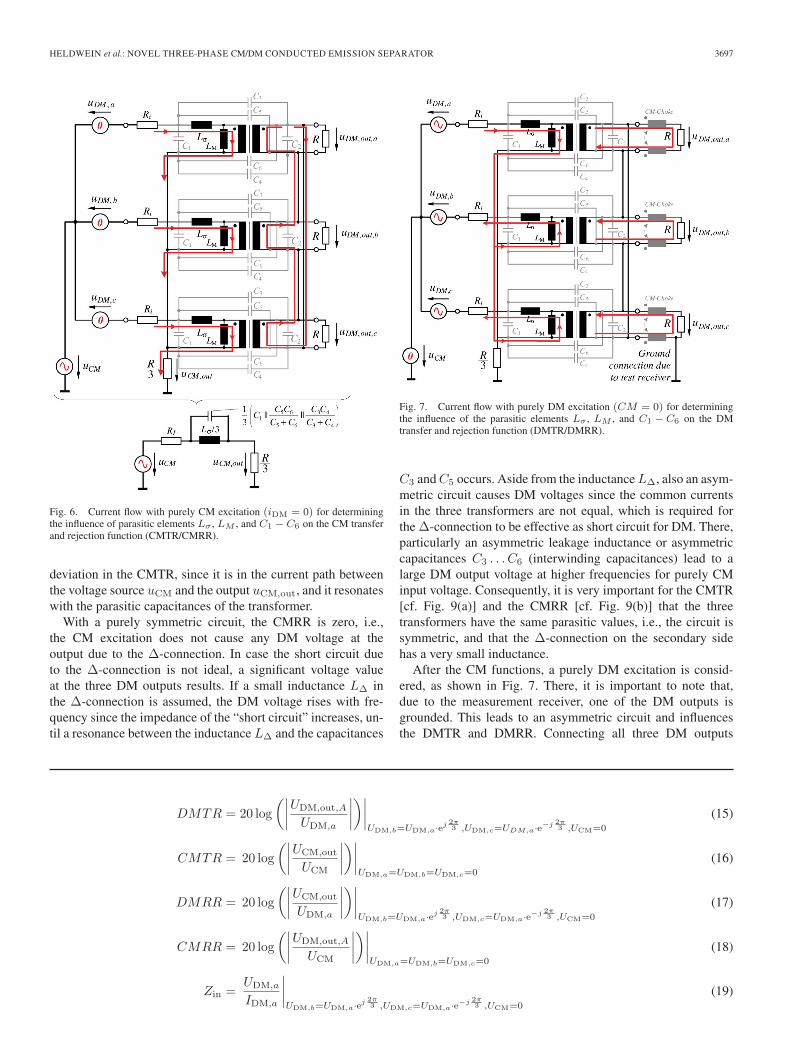
Fig. 9. Influence of parasitic elements on the performance of the separationnetwork. Values if not specified differently: C1 = C2 = −11.6 pF, C3 =C4 = 13.4 pF, C5 = C6 = 13.1 pF, L = 10 mH, Lσ = 190 nH, Lcm = 0,and R = Ri = 50 Ω. Shown: (a) CMTR as function of leakage inductanceand inductance in the Δ-connection; (b) CMRR for the DM outputs fordifferent values of inductance in the Δ-connection; (c) DMTR for the differentDM outputs; (d) DMRR for three different values of the leakage inductanceLσ = 10, 190, and 400 nH; and (e) input impedance for the inputs.
Fig. 10. Circuit schematic of the three-phase CM/DM noise separatorprototype.
Fig. 11. Three-phase CM/DM separator prototype photograph. Overalldimensions: 7.0 × 7.0 × 8.2 cm (2.8 × 2.8 × 3.2 in).
Fig. 12. Calculated flux density in the designed transformers Tra, Trb, andTrc, for a simulated LISN output voltage when feeding a three-phase 5-kWrectifier.
an example. In addition, also the corresponding flux densityin the transformer cores is given. There, the specifications ofa Vaccumschmelze GmbH (VAC) 25 × 16 × 10-T6000-6-L2025-W380 core made of VITROPERM (BSat ≈ 1.2 T) fromVAC and a winding with 10:10 turns have been assumed. In theconsidered case, the peak value of the flux density remains wellbelow the saturation value, but this could vary in dependence

3700 IEEE TRANSACTIONS ON INDUSTRIAL ELECTRONICS, VOL. 56, NO. 9, SEPTEMBER 2009
of the application. In case the input voltage would cause asaturation of the core, an attenuator could be inserted betweenthe LISN and the noise separator. This could also be usedfor testing whether the cores are close to saturation: If thespectrums with and without attenuator are approximately thesame, the core is not close to saturation.
Aside from the basic transformer function, particularly theparasitic elements are important. There, the leakage inductancemust be as small as possible in order not to deteriorate thetransfer functions DMTR and CMTR. Furthermore, the par-asitic capacitance between primary and secondary should besmall, in order to prevent CM paths between primary andsecondary, which influences the CMRR. Furthermore, the pa-rameters should be stable and reproducible, so that a separatorwith symmetric components with respect to the three phasescould be achieved.
The CM chokes in the separator prototype are built with aVAC 12.5 × 10 × 5-T600-6-L2012-W498 core, which alsoconsists of VITROPERM 500 F but is significantly smaller thanthe transformer core. The winding has two times ten turns. Thissetup results in a CM inductance of 1 mH and a resonancefrequency of 30 MHz.
Remark: For applying the separator, a three- or four-lineLISN must allow simultaneous access to all three-phase outputports. In case this is not possible, three individual single-phaseLISNs could be employed. All asymmetries presented in thetest circuit composed of the LISN and the noise separatorwill influence the measurements, particularly in the higherfrequency range, and should be avoided.
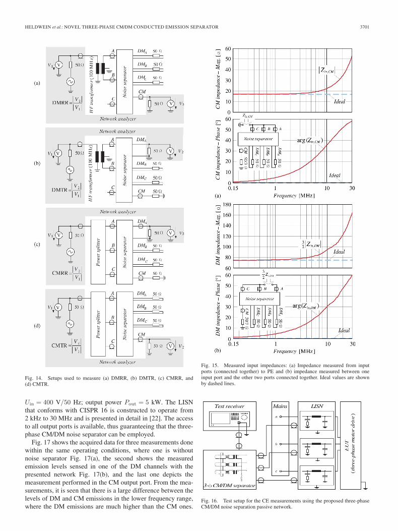
V. EXPERIMENTAL EVALUATION
Some of the frequency response characteristics of the pro-totype were measured with an impedance and a network an-alyzer. These measurements were performed with 50-Ω inputand output impedances. The most significant results of thesemeasurements are shown in Figs. 13 and 15, while the testsetups employed in the measurements are shown in Fig. 14. Asthe noise separator is intended to discriminate CM and DM, it isimportant to check how good the attenuation of the other noisecomponents is, for instance, when measuring a CM signal, theinfluence of the DM channels is needed to be known. This canbe evaluated through the measurement of the DMRR of allchannels and CMRR for the DM channels. The DMRRs of theCM port are shown in Fig. 13(a), and for all cases, it is higherthan 70 dB at 150 kHz and higher than 25 dB up to 30 MHz.The DMTR curves for the three DM channels are quite similar,and only one is shown in Fig. 13(b), where the presented−3-dB cutoff frequency is higher than 20 MHz and goodsymmetry among the channels is observed. The CMRR ofthe DM output ports is shown in Fig. 13(c), showing around50 dB in the lower frequency range and being around 20 dB at10 MHz. In Fig. 13(d), the insertion loss between the measuredCM output voltage and a CM input signal (CMTR) is plotted,and a flatband up to more than 20 MHz is observed. The non-idealities of the circuit also lead to imperfect input impedances(cf., Fig. 15), which increase with increasing frequencies, lead-ing to higher measurement results in the frequency range above
Fig. 13. Measured frequency characteristics for the CM/DM noise separator.(a) DMRR. (b) DMTR. (c) CMRR. (d) CMTR.
10 MHz. The measured frequency characteristics show that theseparation network performs better in the frequency range upto 1 MHz. However, rejection ratios on the order of 30 dB areobserved at 30 MHz, guaranteeing clear separation of the noisemodes.
CE measurements as specified in CISPR 16 were performedby utilizing a setup as shown in Fig. 16 in order to givean example for the use of the three-phase CM/DM separator.The EUT was a regenerative drive feeding a 10-kVA electricmotor. The test conditions were as follows: input voltages
HELDWEIN et al.: NOVEL THREE-PHASE CM/DM CONDUCTED EMISSION SEPARATOR 3701
Fig. 14. Setups used to measure (a) DMRR, (b) DMTR, (c) CMRR, and(d) CMTR.
Uin = 400 V/50 Hz; output power Pout = 5 kW. The LISNthat conforms with CISPR 16 is constructed to operate from2 kHz to 30 MHz and is presented in detail in [22]. The accessto all output ports is available, thus guaranteeing that the three-phase CM/DM noise separator can be employed.
Fig. 17 shows the acquired data for three measurements donewithin the same operating conditions, where one is withoutnoise separator Fig. 17(a), the second shows the measuredemission levels sensed in one of the DM channels with thepresented network Fig. 17(b), and the last one depicts themeasurement performed in the CM output port. From the mea-surements, it is seen that there is a large difference between thelevels of DM and CM emissions in the lower frequency range,where the DM emissions are much higher than the CM ones.
Fig. 15. Measured input impedances: (a) Impedance measured from inputports (connected together) to PE and (b) impedance measured between oneinput port and the other two ports connected together. Ideal values are shownby dashed lines.
Fig. 16. Test setup for the CE measurements using the proposed three-phaseCM/DM noise separation passive network.

3702 IEEE TRANSACTIONS ON INDUSTRIAL ELECTRONICS, VOL. 56, NO. 9, SEPTEMBER 2009
Fig. 17. Measurements performed with and without the noise separator. (Axes) 0 to 100 dB · μV and 150 kHz to 30 MHz. (Upper curves) Quasi-peakmeasurement as specified in CSIPR 16. (Lower curves) Average detection measurement. (a) Measurements applying directly an LISN. (b) Measurementsperformed in one noise separator DM output port. (c) Measurements from the noise separator CM output port.
This indicates the necessity of higher DM attenuation at thisfrequency range. It shows the required attenuation and allowsan appropriate filter to be designed. This example shows that themain purpose of the separator, which is acquiring informationfor filter designs and troubleshooting of power converters,is achieved.
VI. CONCLUSION
This paper has presented two novel three-phase DM/CMseparation networks intended to be used in the evaluation ofnoise sources. The separators’ aim is to help in the design andtroubleshooting of electromagnetic CE control for electronicequipment. One network is an arrangement of passive com-ponents, while the other employs active circuits. The operat-ing principle and characteristics of the passive network werediscussed and experimentally verified. CE measurements weresuccessfully performed in a three-phase electric motor driveusing the separator indicating the noise levels and dominatingmodes. This information could be employed to design the CMand DM stages of an EMC filter.
REFERENCES
[1] H. I. Hsieh, J. S. Li, and D. Chen, “Effects of X capacitors on EMI filtereffectiveness,” IEEE Trans. Ind. Electron., vol. 55, no. 2, pp. 949–955,Feb. 2008.
[2] M. Jin and M. Weiming, “Power converter EMI analysis including IGBTnonlinear switching transient model,” IEEE Trans. Ind. Electron., vol. 53,no. 5, pp. 1577–1583, Oct. 2006.
[3] J.-S. Lai, X. Huang, E. Pepa, S. Chen, and T. W. Nehl, “Inverter EMImodeling and simulation methodologies,” IEEE Trans. Ind. Electron.,vol. 53, no. 3, pp. 736–744, Jun. 2006.
[4] J. Meng, W. Ma, Q. Pan, Z. Zhao, and L. Zhang, “Noise source lumpedcircuit modeling and identification for power converters,” IEEE Trans.Ind. Electron., vol. 53, no. 6, pp. 1853–1861, Dec. 2006.
[5] M. M. Hernando, A. Fernandez, M. Arias, M. Rodriguez, Y. Alvarez, andF. Las-Heras, “EMI radiated noise measurement system using the sourcereconstruction technique,” IEEE Trans. Ind. Electron., vol. 55, no. 9,pp. 3258–3265, Sep. 2008.
[6] C. R. Paul and K. B. Hardin, “Diagnosis and reduction of conductednoise emissions,” IEEE Trans. Electromagn. Compat., vol. 30, no. 4,pp. 553–560, Nov. 1988.
[7] M. J. Nave, “A novel differential mode rejection network for conductedemissions diagnostics,” in Proc. IEEE Nat. Symp. Electromagn. Compat.,1989, pp. 223–227.
[8] M. J. Nave, Power Line Filter Design for Switched-Mode Power Supplies.New York: Van Nostrand Reinhold, 1991.
[9] T. Guo, D. Y. Chen, and F. C. Lee, “Separation of the common-mode- anddifferential-mode-conducted EMI noise,” IEEE Trans. Power Electron.,vol. 11, no. 3, pp. 480–488, May 1996.
[10] K. Y. See, “Network for conducted EMI diagnosis,” Electron. Lett.,vol. 35, no. 17, pp. 1446–1447, Aug. 1999.
[11] S. Wang, F. C. Lee, and W. G. Odendaal, “Characterization, evaluation,and design of noise separator for conducted EMI noise diagnosis,” IEEETrans. Power Electron., vol. 20, no. 4, pp. 974–982, Jul. 2005.
[12] K. Jia, J. Wang, C. Wu, and C. Bi, “A new method for conducted EMInoise diagnosis,” in Proc. 8th Int. Conf. Electron. Meas. Instruments,2007, pp. 4-59–4-63.
[13] M. Mardiguian and J. Raimbourg, “An alternate, complementary methodfor characterizing EMI filters,” in Proc. IEEE Int. Symp. Electromagn.Compat., 1999, pp. 882–886.
[14] L. Ran, J. C. Clare, K. J. Bradley, and C. Christopoulos, “Measurementof conducted electromagnetic emissions in PWM motor drive systemswithout the need for an LISN,” IEEE Trans. Electromagn. Compat.,vol. 41, no. 1, pp. 50–55, Feb. 1999.
[15] A. De Bonitatibus, C. De Capua, and C. Landi, “A new method forconducted EMI measurements on three phase systems,” in Proc. 17thIEEE Instrum. Meas. Technol. Conf., 2000, vol. 1, pp. 461–464.
[16] L. Ran, S. Gokani, J. Clare, K. J. Bradley, and C. Christopoulos,“Conducted electromagnetic emissions in induction motor drive sys-tems. Part I. Time domain analysis and identification of dominantmodes,” IEEE Trans. Power Electron., vol. 13, no. 4, pp. 757–767,Jul. 1998.
[17] W. Shen, F. Wang, D. Boroyevich, and Y. Liu, “Definition and acqui-sition of CM and DM EMI noise for general-purpose adjustable speedmotor drives,” in Proc. IEEE Power Electron. Spec. Conf., 2004, vol. 2,pp. 1028–1033.
[18] T. Nussbaumer, M. L. Heldwein, and J. W. Kolar, “Differential modeinput filter design for a three-phase buck-type PWM rectifier based onmodeling of the EMC test receiver,” IEEE Trans. Ind. Electron., vol. 53,no. 5, pp. 1649–1661, Oct. 2006.
[19] M. L. Heldwein, T. Nussbaumer, and J. W. Kolar, “Differential modeEMC input filter design for three-phase AC–DC–AC sparse matrixPWM converters,” in Proc. IEEE Power Electron. Spec. Conf., Aachen,Germany, 2004, pp. 284–291, [CD-ROM].
[20] IEC Int. Special Committee Radio Interference - C.I.S.P.R., C.I.S.P.R.Specification for Radio Interference Measuring Apparatus and Measure-ment Methods—Publication 16, Geneva, Switzerland, 1977.
[21] J. W. Kolar and H. Ertl, Vorrichtung zur Trennung der Funkstoerspannun-gen dreiphasiger Stromrichtersysteme in eine Gleich-und eine Gegentak-tkomponente, Switzerland, 2004.
[22] F. Beck and W. L. Klampfer, “Measurements of conducted voltage in thelow-frequency range from 2 kHz to 30 MHz for high-current industrialapplications with regeneration drives,” in Proc. Int. Symp. Electromagn.Compat., 2004, vol. 1, pp. 5–10.
[23] J. Biela and J. W. Kolar, “Using transformer parasitics for resonantconverters—A review of the calculation of the stray capacitance of trans-formers,” in Conf. Rec. IEEE IAS Annu. Meeting, Hong Kong, 2005,pp. 1868–1875.

HELDWEIN et al.: NOVEL THREE-PHASE CM/DM CONDUCTED EMISSION SEPARATOR 3703
Marcelo Lobo Heldwein (S’99–M’08) receivedthe B.S. and M.S. degrees in electrical engineer-ing from the Federal University of Santa Catarina,Florianópolis, Brazil, in 1997 and 1999, respectively,and the Ph.D. degree from the Swiss Federal Instituteof Technology (ETH), Zürich, Switzerland, in 2007.
He is currently a Postdoctoral Fellow with thePower Electronics Institute, Federal University ofSanta Catarina, under the PRODOC/CAPES pro-gram, where he was a Research Assistant from 1999to 2001. From 2001 to 2003, he was an Electrical
Design Engineer with Emerson Energy Systems, in São José dos Campos,Brazil, and in Stockholm, Sweden. His research interests include powerfactor correction techniques, static power converters, and electromagneticcompatibility.
Dr. Heldwein is a member of the Brazilian Power Electronics Society.
Jürgen Biela (S’04–M’06) received the Diploma(with honors) in electrical engineering from theFriedrich-Alexander University, Erlangen, Germany,in 2000, and the Ph.D. degree in electrical engineer-ing from the Swiss Federal Institute of Technology(ETH), Zürich, Switzerland, in 2005. In the course ofhis M.Sc. studies, he dealt in particular with resonantdc-link inverters at Strathclyde University, Glasgow,U.K., (term project) and the active control of series-connected integrated gate commutated thyristorsat the Technical University of Munich, Munich,
Germany, (Diploma thesis). In July 2002, he joined the Power ElectronicSystems (PES) Laboratory, ETH Zürich, working toward the Ph.D. degree, con-centrating on an optimized electromagnetically integrated resonant converter.
He was with the Research Department, A&D Siemens, Germany, from 2000to 2001, where he focused on inverters with very high switching frequencies,SiC components, and electromagnetic compatibility. From 2006 to 2007, hewas a Postdoctoral Fellow with PES and has been a Guest Researcher at theTokyo Institute of Technology, Tokyo, Japan. Since 2007, he has been a SeniorResearch Associate with PES, Electrical Engineering Department, ETH Zürich.His current research interests include multidomain modeling, design and opti-mization of PES, particularly systems for future energy distribution and pulsedpower applications, advanced PES based on novel semiconductor technologies,and integrated passive components for ultracompact and ultraefficient convertersystems.
Hans Ertl (M’93) received the Dipl.Ing. (M.Sc.)and Dr.Techn. (Ph.D.) degrees in industrial electron-ics from the Technische Universität Wien, Vienna,Austria, in 1984 and 1991, respectively.
Since 1984, he has been with the Technische Uni-versität Wien, where he is currently an AssociateProfessor of power electronics in the Institute ofElectrical Drives and Machines. He has performednumerous industrial and scientific research projectsin the areas of field-oriented control of ac drivesystems, switch-mode power supplies for welding
and industrial plasma processes, and active rectifier systems. He is the authoror coauthor of numerous scientific papers and patents. His current researchactivities are focused on switch-mode power amplifiers and multicell topolo-gies, particularly for the generation of testing signals, active ripple currentcompensators, and several applications in the area of renewable energy systems.
Thomas Nussbaumer (S’02–M’06) was born inVienna, Austria, in 1975. He received the M.Sc.degree (with honors) in electrical engineering fromthe University of Technology Vienna, Vienna,Austria, in 2001, and the Ph.D. degree from thePower Electronic Systems (PES) Laboratory, SwissFederal Institute of Technology (ETH) Zürich,Zürich, Switzerland, in 2004.
From 2001 to 2006, he was with the PES, wherehe conducted research on modeling, design, and con-trol of three-phase rectifiers, power factor correction
techniques, and electromagnetic compatibility. Since 2006, he has been withLevitronix GmbH, Zürich, Switzerland, where he is currently working onbearingless motors, magnetic levitation, and permanent-magnet motor drivesfor the semiconductor and biotechnology industry. His current research isfocused on compact and high-performance mechatronic systems includingnovel power electronics topologies, control techniques, drive systems, sensortechnologies, electromagnetic interference (EMI), and thermal aspects.
Johann W. Kolar (M’89–SM’04) received the Ph.D.degree (summa cum laude/promotio sub auspiciispraesidentis rei publicae) from the University ofTechnology Vienna, Austria.
Since 1984, he has been an Independent Inter-national Consultant in close collaboration with theVienna University of Technology, in the fields ofpower electronics, industrial electronics, and high-performance drives. On February 1, 2001, he wasappointed as a Professor and Head of the Power Elec-tronic Systems Laboratory, Swiss Federal Institute
of Technology (ETH), Zürich, Switzerland. He has proposed numerous novelPWM converter topologies, and modulation and control concepts, e.g., theVIENNA rectifier and the three-phase ac–ac sparse matrix converter. He haspublished over 300 scientific papers in international journals and conferenceproceedings. He is the holder of 75 patents. His current research is on ac–acand ac–dc converter topologies with low effects on the mains, e.g., for powersupply of telecommunication systems, more electric aircraft, and distributedpower systems in connection with fuel cells. His other main areas of researchinclude the realization of ultracompact intelligent converter modules employinglatest power semiconductor technology (SiC), novel concepts for cooling andEMI filtering, multidomain/multiscale modeling and simulation, pulsed power,bearingless motors, and power MEMS.
Dr. Kolar is a member of the Institute of Electrical Engineers of Japan (IEEJ)and the technical program committees of numerous international conferencesin the field (e.g., Director of the Power Quality Branch of the InternationalConference on Power Conversion and Intelligent Motion). From 1997 to2000, he served as an Associate Editor of the IEEE TRANSACTIONS ON
INDUSTRIAL ELECTRONICS, and since 2001, as an Associate Editor of theIEEE TRANSACTIONS ON POWER ELECTRONICS. Since 2002, he has been anAssociate Editor for the Journal of Power Electronics of the Korean Institute ofPower Electronics and a member of the Editorial Advisory Board of the IEEJTransactions on Electrical and Electronic Engineering. He was the recipientof the Best Transactions Paper Award of the IEEE Industrial ElectronicsSociety in 2005 and an Erskine Fellowship from the University of Canterbury,New Zealand, in 2003. In 2006, the European Power Supplies ManufacturersAssociation awarded the Power Electronics Systems Laboratory of ETH Zürichas the leading academic research institution in Europe.