conducted emission performance of dc/dc power modules
TRANSCRIPT
E
Design Note 009
Conducted Emission Performanceof DC/DC power modules
characterization and system design
General
EMC design is one of the more important challenges for the electronics system designer. Most all equipment types need to meet one or more EMC standards at the system level, and there are many international standards and controlling agencies to deal with. All DC/DC converters contain one or more switching stages which generate a noise spectrum that is capable of leaving the module by conduction and radiation. The radiated path is normally well contained by the standard module and equipment shielding, while the conducted noise often requires some attention from the system designer. Consequently, this design note will focus on conducted emissions. Even though the applicable standards are imposed at the system level rather than at the power module, understand-ing and controlling the conducted emissions performance of the power module is a good beginning to meeting the system level specifi cations.
Unfortunately for the system designer, the available stan-dard DC/DC converters have a wide range of conducted emissions performance. Some contain internal fi ltering and will meet many conducted emission standards without any external components. Others may contain no internal pro-vision for EMC fi ltering and may require an external fi lter at some point in the system in order to meet the applicable standards. Many suppliers of standard DC/DC converters complicate the system designer’s dilemma by providing poor or non-existent specifi cations for the EMC perfor-mance of the converter.
This application note provides useful information to assist the system designer in confi guring a system that meets the required conducted emissions standards. Topics covered include:
• Defi nition of the most widely used conducted emissions requirements.
• Discussion of the internal EMC provisions of various Ericsson power modules.
• Measured results of conducted emissions testing of various power modules.
• Suggestions for external fi ltering solutions for applica-tions demanding low levels of conducted emissions.
• Suggested layout and grounding practices to enhance the EMC performance of power modules.
This is a revised version of a design note that was fi rst released in 2000. This update includes the addition of new product families such as the PKR which is the open-frame version of the PKF, the PKM-E 50W converter and the PKJ-E 100 W converter. Some of the recommended fi lter designs have been improved and simplifi ed by the specifi cation of standard components with second sources. It is now standard practice by Ericsson to include complete EMC data with external fi lter recom-mendations on all datasheets, and this revision of DN009 refl ects this practice.

EN/LZT 146 01 R2A © Ericsson Power Modules AB, January 20062
System requirements
The fi rst step in achieving a sound EMC design is to under-stand the requirements. There are no recognized conducted emissions standards that apply specifi cally to board mount-ed DC/DC converters or power modules. The applicable standards that the system designer must meet are system level standards. That is, the end-use equipment must meet a selected set of conducted emission standards, depending upon the equipment’s usage and the country into which it is sold.
Most equipment has one interface with the power utility, and this is where the conducted emissions standards apply. In-dividual power modules and DC/DC converters are typically isolated from the power line by such items as EMI fi lters, circuit breakers and fuses, transient protection networks and AC/DC front-end power converters. Consequently, any noise conducted from the DC input of a power module does not appear directly at the power line – the noise is modifi ed (usu-ally reduced) by the mentioned components. The result is that the equipment may meet its requirements without any of the DC/DC converters or power modules meeting the EMC standard that is applicable to the equipment.
Many systems will meet all applicable EMC standards by only using the EMC fi lter normally associated with the front-end power supply or the powerline entry fi lter – without any specifi c provision for fi ltering the intermediate DC bus voltage. In other cases, doing some fi ltering at the DC bus voltage level can help the system meet its overall require-ments – often saving cost and complexity by sharing one fi lter between several DC/DC converters or power modules.
Even though individual converters and power modules do not need to meet the conducted emissions EMC standards, it can be constructive to measure their performance relative to such a standard. This provides a common, easily under-stood measurement methodology that can be applied using the same measurement equipment as is used for the end equipment. It also gives a relative measurement of the EMC spectrum of each converter or module so that the equipment designer can make the proper decisions regarding how to meet the system-level requirement.
In spite of the fact that there are many different conducted emissions standards in existence in various countries, the situation is not as complex in practice as it may seem at fi rst glance. Consolidation of requirements within Europe has made the equipment designer’s task much more manage-able. The most commonly used requirements are the CISPR and EN standards for the European market (and adopted by many other markets) and the FCC standards within the US – and these two standards are very similar to each other. Both of them will be discussed here.
The European requirements derive from the International Electrotechnical Commission (IEC). The IEC body respon-sible for EMC requirements is the International Special Com-mittee on Radio Interference (CISPR.), and the requirement that defi nes the strictest limits on conducted emissions is
CISPR 22. These limits are described in the product stan-dards EN55022 and EN55011, which are the correspond-ing European Economic Community requirements. The European standards then defi ne two generic standards for conducted emission limits as a function of environment.
• EN50081-1 European generic emission standard Residential equipment (refers to basic standard EN55022 class B for conducted and radiated noise).
• EN50081-2 European generic emission standard Industrial equipment (refers to basic standard EN55011 class A for conducted and radiated noise).
Residential equipment is typically portable and can be moved around and plugged into various power outlets. Home and offi ce equipment falls into this category. Industrial equipment is more typically “hard-wired” in place and is not portable. The regulations are tighter and more restrictive for residential equipment. EN55022 requirements are shown in Fig. 1 and EN55011 requirements in Fig. 2. In practice, the industrial equipment standard is sometimes referred to as “Class A” while the residential standard is called “Class B” to correspond with the FCC nomenclature to be discussed later.
The requirements are expressed in terms of the noise voltage impressed upon the powerline as a function of frequency, 0.15 to 30 MHz for the European requirements. This is only meaningful if the powerline impedance is known. Consequently, a Line Impedance Stabilization Network (LISN) is specifi ed and used when making the measurement to set the line impedance to 50 ohms. The limits are ex-pressed in terms of voltage decibels relative to 1 microvolt. For example, a measurement of 250 µ V would be expressed as: 20 log 250 = 48 dBµ V.
The European standards give two limits as a function of the type of detector used for the measurement. A higher limit is provided for a quasi-peak detector (less smoothing) and a lower limit for use with an average detector. Both limits must be met for the equipment to pass the requirement.
Fig. 1 – EN55022, FCC Class B domestic requirements
EN 50081-1( )
EN 50081-1( )

EN/LZT 146 01 R2A © Ericsson Power Modules AB, January 2006 3
The FCC limits are also shown in Figs. 1 and 2, and are a few dB lower than the corresponding quasi-peak European requirements. Be aware, however, that language in the FCC standard allows for reduction of some of the quasi-peak measurements if the quasi-peak reading is 6 dB or more higher than the reading with an average detector, making the FCC requirement not as stringent as it appears at fi rst glance. There is also language in the FCC regulation allowing use of the test methodology and limits of EN55022. Thus, as a practical matter, equipment meeting the European standards will be compliant with the FCC requirements. For this reason, we will focus on the EN55022 standards as the baseline requirements for the remainder of this document.
The above has been a generalized discussion. When deter-mining the appropriate standards and test limits for your sys-tem make sure that you consult with the most knowledge-able EMC and regulatory agency people at your company so that the latest regulatory requirements are addressed.
For purposes of future awareness, it should be mentioned that there is a proposed annex to EN50081 that would specify conducted emission limits for DC input systems (i.e. - 48V input Telecom systems) using a different test method-ology than the existing EN50081 requirements and the FCC specifi cations. Because this standard is at this point just a proposal and would require testing with different equip-ment (current measurement rather than voltage), we will not include it in the remainder of the discussion here.
Another standard that is sometimes relevant is EN300 386-2. This standard applies only to Telecommunications network equipment, with either AC or DC inputs. For AC input sys-tems, the requirements in this standard are the same as the EN50081 standards. For DC input systems, the test limits when using an averaging detector are identical to the test limits in EN50081-2. When using a quasi-peak detector for DC input systems, the test limit between 0.15 MHz and 30 MHz is identical to the EN50081-2 requirement, however, the 79 dBµ V limit is extended downward in frequency from 0.15 MHz to 0.02 MHz. Since Ericsson Power Modules have a fundamental operating frequency higher than 0.15 MHz, they easily meet this extended lower frequency requirement. Con-sequently, we will only show data from 0.15 to 30 MHz in this application note. These measurements will, in practice, ensure compliance to both EN50081 and EN300 386-2.
The other most commonly used requirement is the US Federal Communications Commission (FCC) regulation for unintentional radiators as defi ned in part 15J. This standard calls for test methodologies very similar to the European standards, and since the same 50 ohm LISN is used, the same measurement data can be applied to either set of stan-dards. The FCC conducted emission standards begin at 0.45 MHz (rather than the 0.15 MHz of the European standard) and continue to 30 MHz. The limit is expressed in terms of a quasi-peak measurement. As with the European standard, there are two sets of requirements. The “Class A” require-ment corresponds to the European industrial specifi cation and the more restrictive “Class B” is used for equipment that would be measured to the European residential standard.
Internal EMC provisions of power modules
Ericsson power modules are designed with compliance to conducted emission specifi cations as a high priority. All Ericsson power modules include internal fi lters that will even allow the module to meet conducted emission standards as a “stand alone” module without external fi ltering or the positive infl uence of other system elements. Some power modules with a metal case include provision for connecting to the case via a module pin.
The datasheets for recent Ericsson power modules contain extensive information that will defi ne the EMC characteristics of the converter. The nominal operating frequency of the converter is given to assist in understanding the noise spec-trum and to help with external fi lter design, if desired. The actual operating frequency, although fi xed, can vary from the nominal value by up to 20%. The typical module input capacitance is shown, since this must be taken into account when designing external fi lters to interface with the module.
All Ericsson DC/DC converters contain a Pi fi lter on the input that will negate the need for an external fi lter in some cases. The datasheet will specify the location and type of the inter-nal fi lter. Note that some internal inductors are in the positive input leg and some in the negative input leg. Connections to the converter case, when available, are defi ned in the datasheet.
EMC testing is now included as part of the verifi cation test-ing of all new Ericsson power products. Recent Ericsson datasheets include a plot of conducted EMC without an external fi lter. This information is useful in that it shows the spectra of the converter’s operating frequency as well as the effects of synchronous rectifi er FETs on the secondary, which are usually lower in magnitude. The datasheet will also defi ne a suggested external fi lter for meeting EN55022 class B requirements along with a spectral plot of the converter when operated in conjunction with the external fi lter.
Fig. 2 – EN55011, FCC Class A industrial requirements
EN 50081-2(EN 55011)
EN 50081-2(EN 55011)

EN/LZT 146 01 R2A © Ericsson Power Modules AB, January 20064
Testing methodology
In order to provide data that will be as useful, reproducible, and standardized as possible, the power modules were tested in accordance with the most widely accepted industry practices whenever possible. The power module under test is soldered to a printed circuit board 100 by 160 mm in size. The circuit board includes a ground plane that is 87 by 137 mm. Power for the module under test is supplied by a well-regulated, low noise, adjustable AC to DC power supply for the lower power (15W or less) power modules. For higher power modules, a battery bank was used for the DC input in
The 50 µH LISN referred to in the EMC standards presents somewhat of a problem when used in front of high perfor-mance DC/DC converters at the higher power levels. In practice, some of the higher power Ericsson modules will ex-hibit enhanced conducted emission performance with lower values of inductance on the module input. Specifi cally, the PKG series of power modules will give better performance if the value of inductance on the DC input is limited to 10 µH or less.
Keeping the input inductance to less than 10 µH will have the following benefi ts:
• No external capacitor will be required at the module input for the purpose of controlling the input impedance and stability of the converter
order to eliminate the noise source of a high power AC/DC power supply.
The power module is loaded with a passive resistive load to avoid any possible confusion with the noise spectrum from an electronic load. A standard Line Impedance Stabilization Unit (LISN) is connected between both sides of the power source and the power module under test. The LISN sets the resistance from the power module looking back into the power source at the standard value of 50 ohms as defi ned in EN55022, and also provides a standardized connection point for interface to the receiver/spectrum analyzer.
• The measurement will be made in an environment much more representative of the actual system application
Also keep in mind that when testing an actual system us-ing the 50 µH LISN at the system power input, the power module(s) would typically be buffered from the inductance by other system components, such as an AC/DC converter. In that case, the LISN inductance would not have any appre-ciable effect on the conducted emissions performance of the power module(s).
For these reasons, the measurements made for this appli-cation note were done using a 5 µH 50 ohm LISN, which is consistent with the methodology used in the power module datasheets. In practice, meeting the appropriate test limit at the power module level using the data given here should
Fig. 4 – Test Setup for EMC testing

EN/LZT 146 01 R2A © Ericsson Power Modules AB, January 2006 5
external fi ltering network. Differential mode noise appears between the two input power leads of a converter. Common mode noise is present on both input power leads with respect to chassis ground. Common mode noise tends to be the more complex to manage because it requires referencing some points in the fi lter to chassis ground and it is also more likely to create diffi culties with radiated emissions.
Two general types of fi lters are defi ned in this design note - Pi and common mode. The Pi fi lter is effective with differential mode noise and has the advantage of being simpler and less expensive. The common mode fi lters will attenuate common mode noise as well as differential mode noise. These fi lters tend to be more effective, but have the disadvantages of additional cost and complexity and the need to terminate the “Y capacitors” to a nearby earth ground point.
The selection of a fi lter topology is often decided by the architecture of the end-use system. In some telecom systems, for example, the positive DC/DC converter inputs are tied directly to frame ground. In these applications, a Pi fi lter topology can often be used with resulting advantages in simplicity and cost. Some industrial and datacom systems are implemented with a similar architecture, but with the negative input tied to ground, and a Pi fi lter is also suitable here. These types of systems are referred to as “2 wire” or “non-fl oating”.
In systems where the input return is isolated from the frame ground, the common mode fi lter topology is more suitable. The connection of the Y capacitors to the EMC fi lter results in an additional terminal, and these systems are called “3 wire” or “fl oating”.
The table associated with each fi lter design defi nes the component values used and, in some cases, recommended vendors and part numbers for the magnetic components. These fi lter designs can be physically implemented in a very small board area using normal printed circuit board packaging techniques. In practice, one fi lter network, with appropriate attention to current levels, can be used to fi lter more than one power module. For example, many “power per board” distributed systems contain one fi lter near the DC input to the board that provides the fi ltering function for several power modules on the board.
The information above in conjunction with the EMC section of the individual converter datasheets should provide an EMC fi lter solution for most applications. For specialized applications and for a better understanding of fi lter design principles, we offer the following guidance based on Ericsson’s experience with designing EMC fi lters for power conversion products.
Capacitors and inductors are the reactive elements in any EMC fi lter. The impedances as a function of frequency of the capacitors and inductors will determine the fi ltering action. The impedance of an ideal capacitor is given by:
enable meeting the overall system requirement when tested with the 50 µH LISN appropriate for system-level use.
The LISN is connected to the printed circuit board contain-ing the power module by a twisted pair cable 1 m in length. A diagram of the test setup is shown in Fig. 3. Some of the key elements used were:
• DC Power Source: Battery bank
• EMI Receiver: Rohde Schwarz ESHS30 or Spectrum Analyzer Advantest R3131A
• LISN: Solar Electronics 7333-5-TS-50-N or Rohde Schwarz ESH3-Z6
A Windows-based computer system was used to collect and store the data and print the results.
DC/DC power module conductedemissions performance
Figures 9 through 48 show the conducted EMC performance of various Ericsson Power Modules. The measurements were made in the peak mode. The fi rst plot in each set is the performance without any external fi ltering. Note that the “limit” shown on the plots is the “Class B” residential limit and that many of the power modules meet the “Class A” industrial limit without any external fi ltering.
The other plots for each type of power module show the EMC performance with an external fi lter. A total of 8 fi lter designs were used as will be discussed in the next section. As shown in the test results, all module types can be fully compliant to the Class B limits with fairly simple and inexpensive fi lter networks. In most cases, the performance is signifi cantly below the specifi cation requirements.
The EMC performance of the external fi lters was tested using peak detection rather than quasi-peak. This was done to reduce the test time to a reasonable amount. The test results were compared using both methods, and the actual peak levels of the noise spectra were essentially the same with both methods. The only change was in the shape of the waveform in the lower part of the waveform (the area below the test limit).
External filtering
Many systems will meet their product-level conducted emissions requirements with only the normal fi ltering associated with front-end power supplies. To assist the user with the design of systems that have very strict conducted emission requirements, we have included some typical fi lter designs that can be used in conjunction with Ericsson power modules.
There are two categories of conducted emissions from a power module, and it is important to understand the difference between them, as it affects the design of the

EN/LZT 146 01 R2A © Ericsson Power Modules AB, January 20066
XC = 1 / (2 • π • f • C)
where: XC = capacitive reactance in ohms f = frequency in Hertz C = capacitance in Farads
The impedance of an ideal inductor is given by:
XL = 2 • π • f • L
where: XL = inductive reactance in ohms f = frequency in Hertz C = Inductance in Henrys
Unfortunately there are no ideal components. All actual capacitors also contain inductive and resistive elements, and all actual inductors contain capacitive and resistive elements. Basic circuit models of capacitors and inductors containing these parasitic elements are shown in Figure 5.
The inductance, ESL, in physical capacitors is due to unavoidable inductance in the leads, interconnections and physical construction and is referred to as Equivalent Series Inductance. The Equivalent Series Resistance, ESR, of a capacitor is also shown in the model. ESR occurs because there is always some power dissipated in the dielectric and interconnections of a capacitor, which will show up as a resistance in the model. At low frequencies, the capacitive reactance dominates and the overall impedance decreases with frequency. As the operating frequency increases, however, the inductive reactance of ESL eventually becomes equal to the capacitive reactance, and the overall impedance reaches a minimum defi ned by ESR. As frequency
increases further, the inductive reactance dominates and the component no longer behaves as a capacitor. The most useful range of the component is in the couple of frequency decades to the left of the minimum impedance.
When selecting capacitors for use in EMC fi lters, the goal should be to use the smallest value that will meet the fi ltering requirement and to select a capacitor with low ESR. Using the minimum acceptable value will result in a small physical size, good high frequency performance, and a more reasonable cost. The maximum recommended physical size is a 1210 SMT device.
A typical starting value for the capacitor across the input terminals of a fi lter (called the “X capacitor”) is a ceramic capacitor between 0.68 and 1.0 µF. Converters of over 100W may require values between 1.0 and 3.3 µF. The capacitors between the power leads and chassis ground in a common mode fi lter (called the “Y capacitors”) are often in the range of 2.2 to 4.7 nF. The voltage rating of the Y capacitors has to be sized to correspond to the isolation specifi cation for the application – often 1500 volts, for example.
The inductor model shown in Figure 5 helps to explain the actual behavior of real world inductors. Since the inductor is fabricated with one or more windings or traces, it will have some DC resistance, R, which will dissipate power as current fl ows through the inductor. There will also be some stray capacitive coupling between the windings and in the physical packaging of the inductor. The reactance of this parasitic capacitance will determine the high frequency performance limit of the inductor.
Capacitor
Inductor
ESR ESL C
R L
CFrequency
R
Useful Range
Z- o
hms
Z- o
hms
Frequency
ESR
Useful Range
Fig. 5 – EMC fi lter Components
EN/LZT 146 01 R2A © Ericsson Power Modules AB, January 2006 7
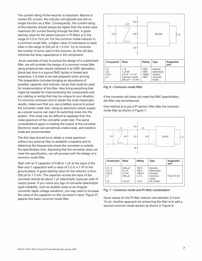
The current rating of the inductor is important. Beyond a certain DC current, the inductor will saturate and will no longer function as a fi lter. Consequently, the current rating of the inductor should always be higher than the worst case maximum DC current fl owing through the fi lter. A good starting value for the series inductor in Pi fi lters is in the range of 3.3 to 10.0 µH. For the common mode inductor in a common mode fi lter, a higher value of inductance is used, often in the range of 250 µH to 1.5 mH. Try to minimize the number of turns used in the inductor, as this will also minimize the stray capacitance in the component.
As an example of how to pursue the design of a customized fi lter, we will consider the design of a common mode fi lter using empirical test results obtained in an EMC laboratory. Since test time in a typical EMC facility is limited and expensive, it is best to be well prepared when arriving. This preparation includes bringing an abundance of possible capacitor and inductor values that could be used for implementation of the fi lter. Also bring everything that might be needed for interconnecting the components and any cabling or wiring that may be unique to your situation. To minimize confusion and to obtain the most meaningful results, make sure that you use a battery source to power the converter under test. Using an electronic power supply as a power source can inject its switching noise into the system. This noise can be diffi cult to separate from the noise spectrum of the converter under test. The same considerations apply to loading the output of the converter. Electronic loads can sometimes create noise, and resistive loads are recommended.
The fi rst step should be to obtain a noise spectrum without any external fi lter to establish a baseline and to determine the frequencies where the converter is outside the specifi cation limit. Assuming that the converter does not meet the specifi cation, we will proceed with the design of a common mode fi lter.
Start with an X capacitor of 0.68 to 1 µF at the input of the fi lter and Y capacitors with a value of 2.2 to 4.7 nF to the ground plane. A good starting value for the inductor is from 250 µH to 1.5 mH. The capacitor across the input of the converter should be about 1 µF (electrolytic type) per watt of output power. If you notice any sign of converter (electrolytic type) instability, such as audible noise or an irregular converter ripple voltage waveform, you may need to increase the value of the capacitor on the converter’s input. Figure 37 depicts this basic common mode fi lter.
If the converter still does not meet the EMC specifi cation, the fi lter may be enhanced.
One method is to put a Pi section fi lter after the common mode fi lter as shown in Figure 7.
Good values for the Pi fi lter inductor are between 3.3 and 10 µH. Another approach for enhancing the fi lter is to add a second common mode section as shown in Figure 8.
Fig. 6 – Common mode fi lter
Component Value Rating Type Suggested part
C1C2C3,4L1
1 μF1 μF/W2.2 nF - 4.7 nFCommon mode250 μH - 1.5 mH
100V100V1500V100V
ceramicelectrolyticceramiccommon mode
Fig. 7 – Common mode and Pi fi lter combination
Component Value Rating Type Suggested part
C1, 2C4, 5C5, 6L1
L2
0.68 μF47 μF2.2 nF768 μH
5.6 μH
100 V100 V1500 V4.7 A
1.6 A
CeramicElectrolyticCeramicCommonmodeDC choke
Pulse PO 422
4

EN/LZT 146 01 R2A © Ericsson Power Modules AB, January 20068
After you fi nd a confi guration that meets your requirements, it is time to optimize the design. In general, you should use the minimum component values that meet the specifi cation with adequate margin. This is especially important for the inductors. The exception to this rule is the capacitor across the converter input. The minimum value for this electrolytic capacitor should be 1 µF per watt of output power to insure stability under all operating conditions.
Occasionally, there may be a problem with oscillations in the EMC fi lter when implemented with low loss components such as low ESR capacitors. While desirable from an effi ciency standpoint, the result is a high Q circuit that is more susceptible to ringing and oscillation. An easy way
to remedy this is to add a resistor across the inductor of the fi lter. A typical value of resistance is 1 to 5 times the impedance of the inductor at the converter’s switching frequency. For example, with a 3.3 µH inductor and a converter operating frequency of 200 kHz, the resistor should be from 4.7 to 22 Ω.
System Layout and Grounding Practices
The EMC performance of the power module itself will not guarantee a successful system. Equally important are the layout and grounding practices used by the system designer for the power module and the power distribution system. Some items that will enhance the system performance include:
• Use adequate decoupling capacitors in the DC distribution system to the load. Include both low frequency bulk capacitance and high frequency ceramic capacitors.
• Use short leads on all fi lter and decoupling components.
• Minimize inductance by using wide distribution traces over ground planes.
• Use separate input and output ground planes, and return common mode noise to the input ground.
More information on the above topics can be found in the Ericsson PowerBook.
Summary
Conducted EMC design does not need to be overly complicated. Understanding the requirements is the fi rst step, and recent consolidation and unifi cation has made this task easier than it was in the past. The information included here on the EMC performance of Ericsson Power Modules will assist the designer in understanding their stand-alone conducted emission characteristics. The system designer should always be aware that additional fi ltering may not be required for many systems, since the other system components such as front-end power supplies often provides all the fi ltering required to meet the specifi c system requirement. In cases where additional fi ltering is required, the suggested fi lter designs presented here ill be a goodstarting point and should streamline the design process.
Fig. 8 – Dual common mode fi lter
Component Value Rating Type Suggested part
C1C2,C3C4,C5C6,C7L1,L2
0.68 μF1.0 μF2.2 nF100 μF810 μΗ
100V100V2000V100V9.7A
ceramicceramicceramicelectrolyticcommon mode inductor
PulsePO 429

EN/LZT 146 01 R2A © Ericsson Power Modules AB, January 2006 9
Fig. 11 – PKF 2111A without fi lter Fig. 12 – PKF 2111A with fi lter B1
Fig. 13 – PKF 2610A without fi lter Fig. 14 – PKF 2610A with fi lter B1
Filter Component Value Rating Type
B 1 C1, 2C3, 4L1
0.68 μF10 nF50 μH
100 V1500 A0.5 A
CeramicCeramic
B 2
≤10W
C1, C2C2C3, C4L1
1 μF10 μF2.2 nF1.17 mH
100 V100 V1500 V1.22 A
Common modeElectrolyticCeramicCommon mode
PulsePO 354
B 3 C2 47 μF 100 V Electrolytic
Fig. 10 – Common mode fi lter (B) for PKF/PKR and PKVFig. 9 – Pi-fi lter (A) for PKF, PKC
Filter Component Value Rating Type Suggested part
A C1, 2L1
0.68 μF10 μH
100 V0.5 A
CeramicDC choke

EN/LZT 146 01 R2A © Ericsson Power Modules AB, January 200610
Fig. 15 – PKF 4611 without fi lter Fig. 16 – PKF 4611 with fi lter A
Fig. 17 – PKR 4110B without fi lter Fig. 18 – PKR 4110B with fi lter B3
Fig. 19 – PKR 4211A without fi lter Fig. 20 – PKR 4211A with fi lter B2
EN/LZT 146 01 R2A © Ericsson Power Modules AB, January 2006 11
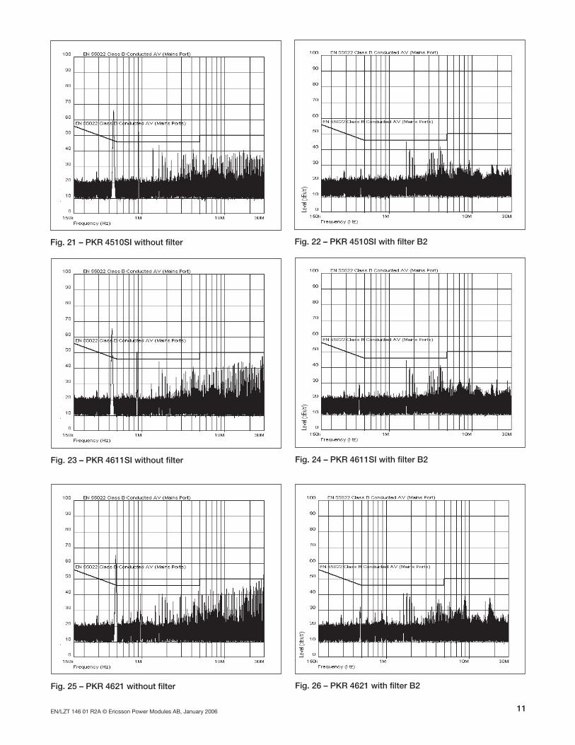
Fig. 21 – PKR 4510SI without fi lter Fig. 22 – PKR 4510SI with fi lter B2
Fig. 23 – PKR 4611SI without fi lter Fig. 24 – PKR 4611SI with fi lter B2
Fig. 25 – PKR 4621 without fi lter Fig. 26 – PKR 4621 with fi lter B2

EN/LZT 146 01 R2A © Ericsson Power Modules AB, January 200612
Fig. 27 – PKR 4713SI without fi lter Fig. 28 – PKR 4713SI with fi lter B2
Fig. 29 – PKR 4910A without fi lter Fig. 30 – PKR 4910A with fi lter B2
Fig. 31 – PKR 5113 without fi lter Fig. 32 – PKR 5113 with fi lter B2

EN/LZT 146 01 R2A © Ericsson Power Modules AB, January 2006 13
Fig. 36 – PKV 5211 with fi lter B2 Fig. 35 – PKV 5211 without fi lter
Fig. 33 – PKV 3211 without fi lter Fig. 34 – PKV 3211 with fi lter B2

EN/LZT 146 01 R2A © Ericsson Power Modules AB, January 200614
Fig. 38 – Common mode fi lter (D) for PKJFig. 37 – Common mode fi lter (C) for PKG
Filter Component Value Rating Type Suggested part
C C1, 2C3C4,5L1
0.68 μF47 μF3.9 nF425 μH
100 V100 V1500 V3 A
CeramicElectrolyticCeramicCommonmode
Coilcraft P3217ATDK TF1028S 451
Filter Component Value Rating Type Suggested part
D C1, 2, 4C3, 5C6, 7C8L1
L2, 3
0.68 μF47 μF3.9 nF4.7 nF425 μH
22 μH
100 V100 V1500 V1500 V4.7 A
4.7 A
CeramicElectrolyticCeramicCeramicCommonmode
DC choke
Coilcraft P3217ATDK TF1028S-361Y4R7-01CoilcraftDO5022P-223
Fig. 42 – PKG 4611 with fi lter C
Fig. 39 – PKG 2611 without fi lter Fig. 40 – PKG 2611 with fi lter C
Fig. 41 – PKG 4611 without fi lter
EN/LZT 146 01 R2A © Ericsson Power Modules AB, January 2006 15
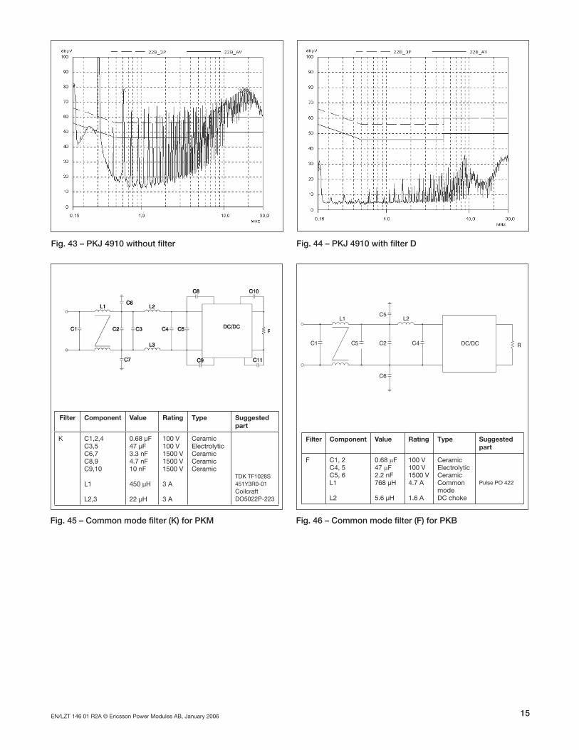
Fig. 43 – PKJ 4910 without fi lter Fig. 44 – PKJ 4910 with fi lter D
Fig. 45 – Common mode fi lter (K) for PKM Fig. 46 – Common mode fi lter (F) for PKB
Filter Component Value Rating Type Suggested part
K C1,2,4C3,5C6,7C8,9C9,10
L1
L2,3
0.68 µF47 µF3.3 nF4.7 nF10 nF
450 µH
22 µH
100 V100 V1500 V1500 V1500 V
3 A
3 A
CeramicElectrolyticCeramicCeramicCeramic
TDK TF1028S451Y3R0-01Coilcraft DO5022P-223
Filter Component Value Rating Type Suggested part
F C1, 2C4, 5C5, 6L1
L2
0.68 μF47 μF2.2 nF768 µH
5.6 µH
100 V100 V1500 V4.7 A
1.6 A
CeramicElectrolyticCeramicCommonmodeDC choke
Pulse PO 422
4

EN/LZT 146 01 R2A © Ericsson Power Modules AB, January 200616
Fig. 48 – PKM 4610 with fi lter KFig. 47 – PKM 4610 without fi lter
Fig. 50 – PKB 4610 with fi lter F
100
90
80
70
60
50
40
30
20
10
0
0.15 1.0 10.0 30.0MHz
22B_QP 22B_AVdBµV
Fig. 49 – PKB 4610 without fi lter
100
90
80
70
60
50
40
30
20
10
0
0.15 1.0 10.0 30.0MHz
22B_QP 22B_AVdBµV

EN/LZT 146 01 R2A © Ericsson Power Modules AB, January 2006 17
Fig. 51 – Common mode fi lter for (G) PKM2000E, (H)PKM4000E, PKJ4000E
Filter Component Value Rating Type Suggestedpart
G C1, 2, 3C4C5, 6L1
L2
0.68 μF220 μF3.9 nF768 μH
47 μH
100 V63 V1500 V4.7 A
3.3 A
CeramicElectrolyticCeramicCommonmodeDC choke
Pulse PO 422
H C1, 2, 3C4, 7C5, 6, L1
L2
0.68 μF47 μF3.9nF768 μH
15 μH
100 V100 V1500 V4.7 A
3.3 A
CeramicElectrolyticCeramicCommonmodeDC choke
Pulse PO 422
Fig. 53 – 2510 EPI with fi lter GFig. 52 – PKM 2510 EPI without fi lter

EN/LZT 146 01 R2A © Ericsson Power Modules AB, January 200618
Fig. 55 – PKM 4510 EPI with fi lter HFig. 54 – PKM 4510 EPI without fi lter
Fig. 57 – PKJ 4810 EPI with fi lter HFig. 56 – PKJ 4810 EPI without fi lter

EN/LZT 146 01 R2A © Ericsson Power Modules AB, January 2006 19
Fig. 44 – Two wire fi lter (L)
Filter Component Value Rating Type Suggested part
L C1, 2, 3 C4, 5, 6L1, L2
2.2 μF100 μF5.6 μH
100 V100 V3.5 A
ceramicelectrolyticDC choke
Fig. 45 – PKJ 4810 EPIP without fi lter Fig. 46 – PKM 4810 EPIP with fi lter
Fig. 47 – PKJ 4111 EPIP without fi lter Fig. 48 – PKJ 4111 EPIP with fi lter

EN/LZT 146 01 R2A© Ericsson Power Modules AB, January 2006
The latest and most complete infor-mation can be found on our website!
Ericsson Power Modules AmericasSE-126 25 Stockholm, Sweden Ericsson Inc., Power ModulesTelephone: +46 8 568 69620 +1-972-583-5224, +1-972-583-6910
For local sales contacts, please refer to our website Asia/Pacifi cwww.ericsson.com/powermodules Ericsson Ltd.or call: Int +46 8 568 69620, Fax: +46 8 568 69599 +852-2590-2453