notice changes introduced as a result of publishing...
TRANSCRIPT

This is the author’s version of a work that was submitted/accepted for pub-lication in the following source:
Zhan, Haifei, Zhang, Gang, Bell, John M., & Gu, YuanTong(2014)Thermal conductivity of configurable two-dimensional carbon nanotube ar-chitecture and strain modulation.Applied Physics Letters, 105, p. 153105.
This file was downloaded from: https://eprints.qut.edu.au/77902/
c© Copyright 2014 AIP Publishing LLC
Notice: Changes introduced as a result of publishing processes such ascopy-editing and formatting may not be reflected in this document. For adefinitive version of this work, please refer to the published source:
https://doi.org/10.1063/1.4898578
1
Thermal Conductivity of Configurable Two-dimensional Carbon Nanotube
Architecture and Strain Modulation
H.F. Zhan1, G. Zhang2, J. M. Bell1 and Y.T. Gu*,1
1School of Chemistry, Physics and Mechanical Engineering, Queensland University
of Technology, 2 George St, Brisbane QLD 4109, Australia
2Institute of High Performance Computing, Agency for Science, Technology and
Research, 1 Fusionopolis Way 138632, Singapore
*Corresponding Author: Prof. Yuantong Gu
Mailing Address: School of Chemistry, Physics and Mechanical Engineering,
Queensland University of Technology,
GPO Box 2434, Brisbane, QLD 4001, Australia
Telephones: +61-7-31381009 Fax: +61-7-31381469
E-mail: [email protected]

2
Abstract
We reported the thermal conductivity of the two-dimensional carbon nanotube
(CNT)-based architecture, which can be constructed through welding of single-wall
CNTs by electron beam. Using large-scale nonequilibrium molecular dynamics
simulations, the thermal conductivity is found to vary with different junction types
due to their different phonon scatterings at the junction. The strong length and strain
dependence of the thermal conductivity suggests an effective avenue to tune the
thermal transport properties of the CNT-based architecture, benefiting the design of
nanoscale thermal rectifiers or phonon engineering.
Keywords: thermal conductivity. nanoarchitecture, carbon nanotube, tensile strain
Introduction
Carbonaceous nanomaterials, such as carbon nanotube (CNT) and graphene have
attracted huge interests from both scientific and engineering communities due to their
outstanding mechanical, electronic, chemical, thermal, and other properties. It has
been found that the thermal conductivity of carbon materials can range from ~ 0.01
W/mK in amorphous carbon to above 2000 W/mk,1 demonstrating an five order
allowable tuning ranges for the thermal conductivity. In this regard, a comprehensive
understanding of the thermal transport properties of carbonaceous nanomaterials is
crucial for the design of next generation of nano-devices. For instance, electronic,
optoelectronic and photonic devices demand efficient heat removal so as to maintain
their operating performance and long-term reliability. Whereas, the thermoelectric
devices, requires materials with strongly suppressed thermal conductivity to ensure a
3
high figure of merit, ZT=S2σT/κ (here, S is the Seebeck coefficient, T is the
temperature, and σ and κ are the electrical and thermal conductivity, respectively).
Recent decades have witnessed an increasing researches aiming to explore the
effective avenues to modulate the thermal conductivity of carbonaceous materials. For
example, researchers have examined the impacts from the geometry size,2 structure,3, 4
and doping/heteroatoms5 on the thermal properties of graphene. Despite the low
dimensional nanomaterials, many attempts have also been made to develop more
complex nanostructures basing on graphene and nanotube. For example, Zhu et al.6
reported the synthesisation of seamless 3D carbon nanotube graphene hybrid material.
Such pillared-graphene structure is reported with tailorable in-plane and out-of-plane
thermal transport properties.7 Earlier studies reveal that under high temperatures, two
single wall CNTs (SWNTs) can be welded by electron beam and resulting X-, Y-, or
T-like junctions.8, 9 Employing these junctions as building blocks, a variety of
different 2D or 3D CNT-based nanoarchitectures can be constructed.10, 11
To date, several works have been reported on the CNT-based nano-
architectures, which have focused on their mechanical properties, such as the bending
rigidity and shear stiffness,12 rupture strain,13 toughness and stiffness,14 and their
thermal transport properties are still lacking of understanding. In this regard, we
conduct such a study to assess the thermal conductivity of 2D CNT-based
architectures basing on large-scale molecular dynamics (MD) simulations. It is found
that different junction types will endow the associated structures with different
thermal conductivities, and the length of the structure as well as the axial strain can be
employed as an effective way to tune their thermal conductivity.

4
Methods
To assess the thermal conductivity of 2D SWNT architecture, a series of reverse non-
equilibrium molecular dynamics (RNEMD) simulations were performed by using the
Large-scale Atomic/Molecular Massively Parallel Simulator (LAMMPS).15 The idea
of RNEMD is to divide the sample into several slabs along its length direction, and
then exchanging the velocity of the hottest atom in the “cold” slab with the coldest
atom in the “hot” slab.16 This exchange scheme will generate an artificial heat flux to
the sample and thus result in a temperature gradient as illustrated in Figure 1.
Figure 1 A stable temperature profile obtained from RNEMD simulation.
The heat flux J (in unit of Watt) that involves with a certain simulation time t
can be calculated from, 2 21 2 ( )2 hot cold
N
mJ tA v v= −∑ . Here A is the cross-sectional area,
N is the total number of exchanges, m is the atomic mass, hotv and coldv are the
velocities of the hot and cold atoms in the “cold” and “hot” slabs, respectively. The
factor 2 in the denominator is used to account for the periodicity of the system. A
steady state regime will arrive after certain exchanges, after which, the thermal
conductivity (κ) can be calculated by following the Fourier’s law, / ( / )J T xκ = − ∂ ∂ .
Here /T x∂ ∂ is the temperature gradient along the heat flux direction, which can be
estimated from the temperature profile.
5
Different 2D SWNT architecture models have been considered, which are
constructed from (6,6) SWNTs. The interactions between the bonded carbon atoms
were described by the widely used adaptive intermolecular reactive empirical bond
order (AIREBO) potential,17 which has been shown to well represent the binding
energy and elastic properties of carbon materials. A small time step of 0.5 fs was
chosen. The initial equilibrium configuration of the sample was achieved by the
conjugate gradient minimization method. Then the sample was equilibrated using
Nose-Hoover thermostat18, 19 under an ambient condition for 500 ps (temperature =
300 K and pressure = 1 atm). Finally, the system was switched to the microcanonical
ensemble for 3 ns. Periodic boundary condition is only applied along the length
direction.
Results and Discussion.
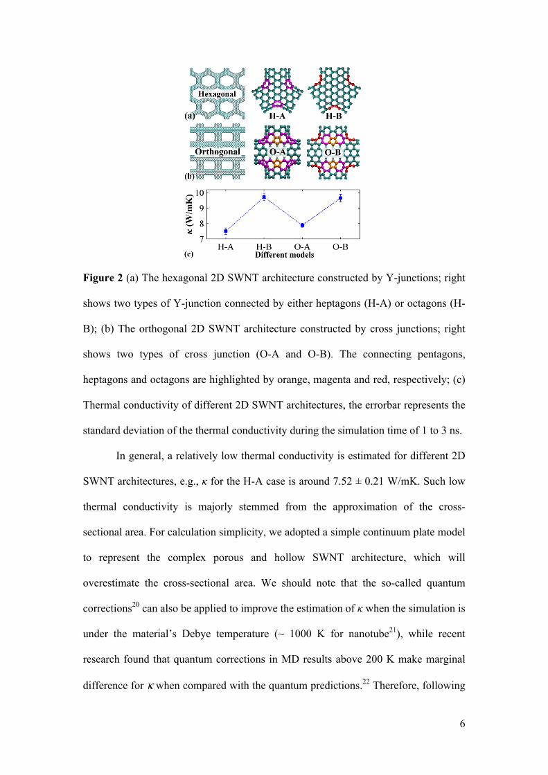
Structural influence. At the beginning, we investigate how the thermal conductivity
will alter with different structures. Two types of 2D architectures have been
constructed, i.e., hexagonal and orthogonal, which are generated by repeating Y-
junctions and cross junctions in the two lateral directions, respectively (see Figure 2a
and 2b). Specifically, the Y-junction is comprised by connecting three (6,6) SWNTs
with an angle of 120° through either heptagons or octagons, and the cross junction is
comprised by connecting four (6,6) SWNTs with an angle of 90° through a
combination of pentagons, heptagons, and octagons.11 To avoid the influence from
geometry size, a similar size has been chosen for all models, ~ 64 × 10 nm2. The
thickness of all models is determined by the diameter of the constituent (6,6) SWNT,
which approximates to 0.9 nm.
6
Figure 2 (a) The hexagonal 2D SWNT architecture constructed by Y-junctions; right
shows two types of Y-junction connected by either heptagons (H-A) or octagons (H-
B); (b) The orthogonal 2D SWNT architecture constructed by cross junctions; right
shows two types of cross junction (O-A and O-B). The connecting pentagons,
heptagons and octagons are highlighted by orange, magenta and red, respectively; (c)
Thermal conductivity of different 2D SWNT architectures, the errorbar represents the
standard deviation of the thermal conductivity during the simulation time of 1 to 3 ns.
In general, a relatively low thermal conductivity is estimated for different 2D
SWNT architectures, e.g., κ for the H-A case is around 7.52 ± 0.21 W/mK. Such low
thermal conductivity is majorly stemmed from the approximation of the cross-
sectional area. For calculation simplicity, we adopted a simple continuum plate model
to represent the complex porous and hollow SWNT architecture, which will
overestimate the cross-sectional area. We should note that the so-called quantum
corrections20 can also be applied to improve the estimation of κ when the simulation is
under the material’s Debye temperature (~ 1000 K for nanotube21), while recent
research found that quantum corrections in MD results above 200 K make marginal
difference for κ when compared with the quantum predictions.22 Therefore, following
7
discussions are emphasized on the relative value of the thermal conductivity, and
quantum corrections are neglected in this work. According to Figure 2c, different
junction types will result in different thermal conductivities and the nanoarchitecture
with octagons (H-B and O-B) are found to have a larger thermal conductivity
comparing with their counterparts without octagons. For instance, κ of H-B is around
30% larger than that of H-A.
To unveil the underneath mechanisms, we computed the vibrational density of
states (VDOS) for the different 2D CNT-based structures, basing on the Fourier
transformation of the autocorrelation function of the atomic velocities.23 Considering
that the heat is mostly carried by the in-plane longitudinal acoustic (LA), in-plane
transverse acoustic (TA) phones, and out-of-plane acoustic (ZA) phonons, we
decomposed the total VDOS into the in-plane and out-of-plane spectra by using the
atomic velocity components in these corresponding directions. According to Figure
3a, the in-plane phonon modes of the architectures with octagons show higher peaks
for both hexagonal and orthogonal structures. Similar results are also observed for the
out-of-plane phonon modes as shown in Figure 3b. These observations explained that
the 2D CNT-based structures which contain octagons possess higher thermal
conductivity. Considering the ballistic nature of heat propagation in the architecture,
the different thermal conductivities are originated from the different phonon
scatterings at the junctions as indicated by the mismatches of the VDOS between the
CNT and junction regions in Figure 3c and 3d. To note that the two orthogonal
structures (O-A and O-B) shows much smaller amplitudes for the high-frequency
phonon modes comparing with that of the hexagonal structures in Figure 3a. Whereas,
the estimated κ does not follow such pattern, indicating certain inconsistencies with
the Debye model for the specific heat of acoustic phonons,24 i.e., smaller amplitudes

8
of the high-frequency phonon modes indicate smaller overall thermal conductivity.
Such inconsistency is originated from the geometry size of different samples, which is
not identical due to the nature of different junctions, while the sample sizes (along
both lateral and longitudinal directions) exert significant impacts to the κ as discussed
below.
Figure 3 The VDOS of different structures for: (a) in-plane phonons; and (b) out-of-
plane phonons; VDOS comparison between CNT and junction regions for: (c) sample
H-A; and (d) sample H-B (the CNT and junction regions in a Y-junction unit has been
selected for the VDOS computation).
Length dependence. We examine the length dependence of the thermal conductivity
by considering the 2D SWNT architectures constructed by H-A Y-junction with an
identical cross-sectional size of ~ 10 × 1 nm2 and length ranging from 53 to 77 nm.
As shown in Figure 4, a strong length dependent thermal conductivity is observed, the
inverse of which exhibits a linear relation with the inverse of the sample length. Such
phenomenon is in line with the common heuristic argument that when the periodic
length of the simulation cell L is smaller than the phonon mean-free path Λ (Λ ~700-
750 nm for SWNT at room temperature1), the inverse of thermal conductivity is
proportional to the frequency of scattering events, with contributions from the sample
ends and from intrinsic scattering,25 i.e., 1 / 1 / 1 / Lκ Λ∝ + . Apparently, by
extrapolating the linear trend to L�� (i.e., 1 / 0L : ), the thermal conductivity will be

9
irrelevant or independent to the sample length L, approaching the limit thermal
conductivity for a macroscopic 2D CNT nanoarchitecture κ∞ . From Figure 4, the
limit of thermal conductivity for the 2D SWNT architecture (constructed by H-A Y-
junction) is estimated as 8.5κ∞ = W/mK, i.e., κ will saturate to κ∞ at 300 K while
the sample size is much larger than the phonon mean-free path, changing from
ballistic to diffusive phonon-transport regime.
Figure 4 Thermal conductivity of the 2D SWNT architecture as a function of length.
Strain impacts. Further, we investigate the strain influence on the κ of the 2D SWNT
architectures. A constant strain rate of 0.2 ns-1 was applied to the structure to achieve
different strain values. Here the strain is defined as 0 0( ) /L L Lε = − ( 0L and L
representing the initial and deformed length of the structure, respectively), and the
atomic stress is computed basing on Virial stress.26 It is worthy to mention that when
the C-C bonds are stretched beyond 1.7 Å, a 1.7 Å cutoff distance for the AIREBO
potential would lead to spuriously high tensile force. As suggested by previous
researchers, a 2.0 Å cutoff can be chosen to overcome such abnormal phenomenon.27
Though such phenomenon is also observed in the 2D CNT-based structures, our
simulations reveal that the change of cutoff distance from 1.7 Å to 2.0 Å exert
marginal influence to the elastic deformation of the structure (ε < ~ 9.5%, see Figure
5a). As expected, the constituent CNTs of the H-A architecture are compressed along
10
the lateral direction while stretched along the length direction due to the tensile
loading, reflecting the possion’s ratio of the structure (refer to left inset of Figure 5a).
Specifically, all C-C bonds around the stretched region are smaller than the initial 1.7
Å cutoff distance at the strain of 9% (see right inset of Figure 5a). Therefore, a cutoff
distance of 1.7 Å is chosen for the tensile deformation to achieve a pre-strained
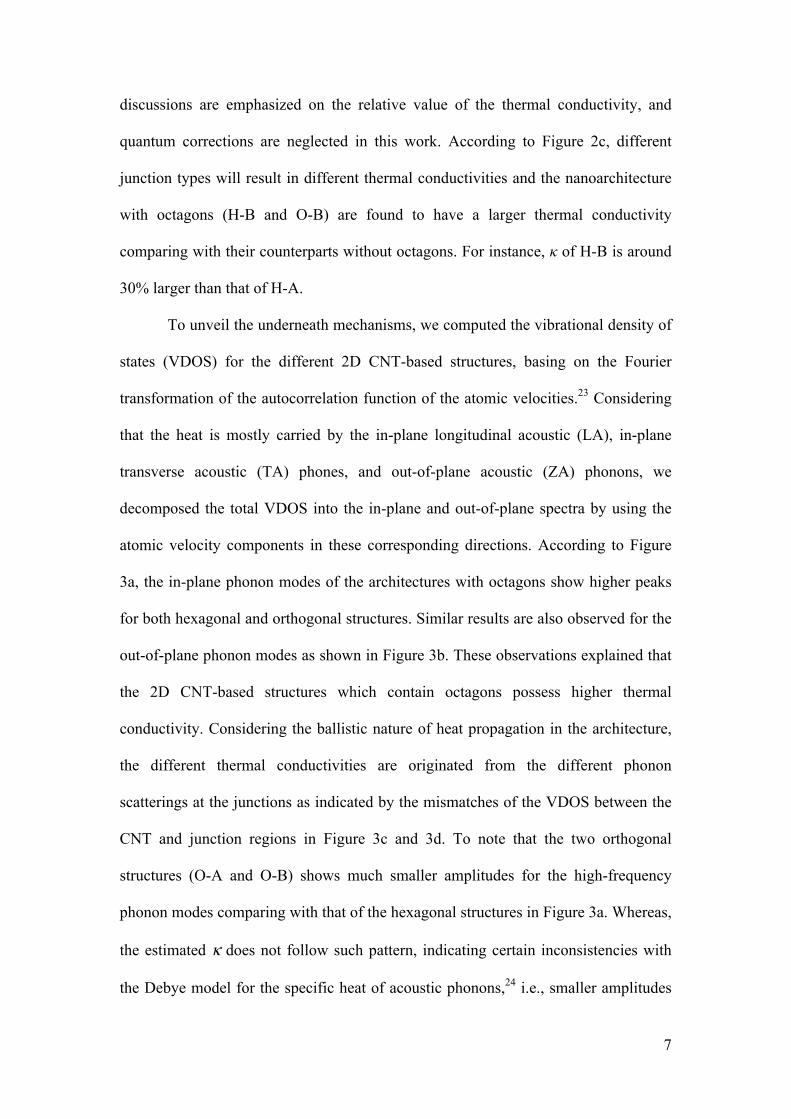
structure for discussion consistency.
Figure 5 (a) Stress-strain curve of the 2D SWNT architectures made from H-A & O-
A junctions, left inset shows the atomic stress (in the unit of GPa⋅Å3) distribution in
the H-A architecture at 9% strain, right inset shows the corresponding bond length
distribution for a Y-junction cell; (b) The relative thermal conductivities of H-A & O-
A architectures as a function of strain; (c) The total VDOS of H-A architecture under
the axial strain of 0, 0.04, 0.06 and 0.08.
Figure 5b shows that the thermal conductivities of the 2D SWNT architectures
decrease monotonically with increasing axial strain. For instance, a 8% axial strain is
found to induce ~ 30% (~ 20%) reduction to the κ of H-A (H-B) structure. Such
observations are in line with the results reported for CNT28 and graphene nano-
ribbon.29 According to the kinetic theory, the thermal conductivity of a solid can be
expressed as Cλ λ λλκ υ Λ=∑ , where λ is the phonon mode index. C and υ are the
11
specific heat and group velocity of each phonon mode, respectively. The existence of
axial tensile strain will soften the high-frequency phonon modes (i.e., the G-peak, see
Figure 5c), which decreases specific heat and thus lead to a reduction to κ.30
Interestingly, Figure 5b suggests that the axial strain induces larger reduction to κ for
the H-A structure with a lower Young’s modulus (as seen in the stress-strain curve in
Figure 5a). It can be concluded that the thermal transport properties of the 2D CNT-
based structures can be effectively tailored through the modulation of axial strain.
Conclusions
In summary, basing on large-scale nonequilibrium molecular dynamics simulations,
the thermal conductivity of 2D SWNT-based structures has been studied. Under high
temperature, the feasibility of welding SWNTs into network structures by electron
beam suggests an appealing way for the thermal properties engineering for carbon-
based nanoarchitectures. It is found that the length of the architecture as well the axial
strain can be employed as an effective way to tune its corresponding thermal
conductivity. For instance, a 8% axial strain can induce ~30% reduction to the
thermal conductivity of the 2D SWNT architecture. This study sheds lights on the
nanoscale thermal/phonon engineering by utilizing SWNTs.
Acknowledgments
Supports from the ARC Discovery Project (DP130102120) and the High Performance
Computer resources provided by the Queensland University of Technology are
gratefully acknowledged. Dr Zhan is grateful to Dr Zhou from Hefei University of
Technology (China) for providing the advices in constructing the models.

12
References
1. A. A. Balandin, Nat. Mater. 10 (8), 569-581 (2011). 2. D. L. Nika, A. S. Askerov and A. A. Balandin, Nano Lett. 12 (6), 3238-3244
(2012). 3. J. Hu, X. Ruan and Y. P. Chen, Nano Lett. 9 (7), 2730-2735 (2009). 4. H. Zhan, Y. Zhang, J. M. Bell, Y.-W. Mai and Y. Gu, Carbon 77, 416-423
(2014). 5. Q. X. Pei, Y. W. Zhang, Z. D. Sha and V. B. Shenoy, Appl. Phys. Lett. 100
(10), 101901 (2012). 6. Y. Zhu, L. Li, C. Zhang, G. Casillas, Z. Sun, Z. Yan, G. Ruan, Z. Peng, A.-R.
O. Raji and C. Kittrell, Nat. Commun. 3, 1225 (2012). 7. V. Varshney, S. S. Patnaik, A. K. Roy, G. Froudakis and B. L. Farmer, ACS
Nano 4 (2), 1153-1161 (2010). 8. M. Terrones, Annu. Rev. Mater. Res. 33 (1), 419-501 (2003). 9. L. P. Biró, Z. E. Horváth, G. I. Márk, Z. Osváth, A. A. Koós, A. M. Benito,
W. Maser and P. Lambin, Diamond Relat. Mater. 13 (2), 241-249 (2004). 10. V. R. Coluci, D. S. Galvao and A. Jorio, Nanotechnology 17 (3), 617 (2006). 11. R. Zhou, R. Liu, L. Li, X. Wu and X. C. Zeng, J. Phys. Chem. C 115 (37),
18174-18185 (2011). 12. L. Ying, Q. XinMing, Y. Fan, W. Xi-Shu, Y. Yajun and F. Qinshan, J. Phys.
D: Appl. Phys. 41 (15), 155423 (2008). 13. Z. Qin, X.-Q. Feng, J. Zou, Y. Yin and S.-W. Yu, Appl. Phys. Lett. 91 (4),
043108 (2007). 14. M. P. Nicola, Nanotechnology 17 (21), 5480 (2006). 15. S. Plimpton, J. Comput. Phys. 117 (1), 1-19 (1995). 16. F. Muller-Plathe, J. Chem. Phys. 106 (14), 6082-6085 (1997). 17. D. W. Brenner, O. A. Shenderova, J. A. Harrison, S. J. Stuart, B. Ni and S. B.
Sinnott, J. Phys.: Condens. Matter 14 (4), 783 (2002). 18. W. G. Hoover, Phys. Rev. A 31 (3), 1695-1697 (1985). 19. S. Nosé, J. Chem. Phys. 81, 511 (1984). 20. C. Wang, C. Chan and K. Ho, Phys. Rev. B 42 (17), 11276 (1990). 21. T. Tohei, A. Kuwabara, F. Oba and I. Tanaka, Phys. Rev. B 73 (6), 064304
(2006). 22. J. Turney, A. McGaughey and C. Amon, Phys. Rev. B 79 (22), 224305
(2009). 23. J. Dickey and A. Paskin, Phys. Rev. 188 (3), 1407 (1969). 24. E. Pop, V. Varshney and A. K. Roy, MRS Bull. 37 (12), 1273-1281 (2012). 25. P. K. Schelling, S. R. Phillpot and P. Keblinski, Phys. Rev. B 65 (14), 144306
(2002). 26. J. Diao, K. Gall and M. L. Dunn, J. Mech. Phys. Solids 52 (9), 1935-1962
(2004). 27. O. A. Shenderova, D. W. Brenner, A. Omeltchenko, X. Su and L. H. Yang,
Phys. Rev. B 61 (6), 3877-3888 (2000). 28. X. Zhiping and J. B. Markus, Nanotechnology 20 (18), 185701 (2009). 29. W. Ning, X. Lanqing, W. Hui-Qiong and Z. Jin-Cheng, Nanotechnology 22
(10), 105705 (2011). 30. J. Chen, J. H. Walther and P. Koumoutsakos, Nano Lett. 14, 819-825 (2014).