nanoarchitectures – spring 2005copyright vijay cse 598 nanoarchitectures spring 2005 lecture 1:...
TRANSCRIPT
Nanoarchitectures – Spring 2005 copyright Vijay
CSE 598 Nanoarchitectures
Spring 2005
Lecture 1: IntroductionVijay Narayanan (www.cse.psu.edu/~vijay)
Nanoarchitectures – Spring 2005 copyright Vijay
Nanoarchitectures – Spring 2005 copyright Vijay
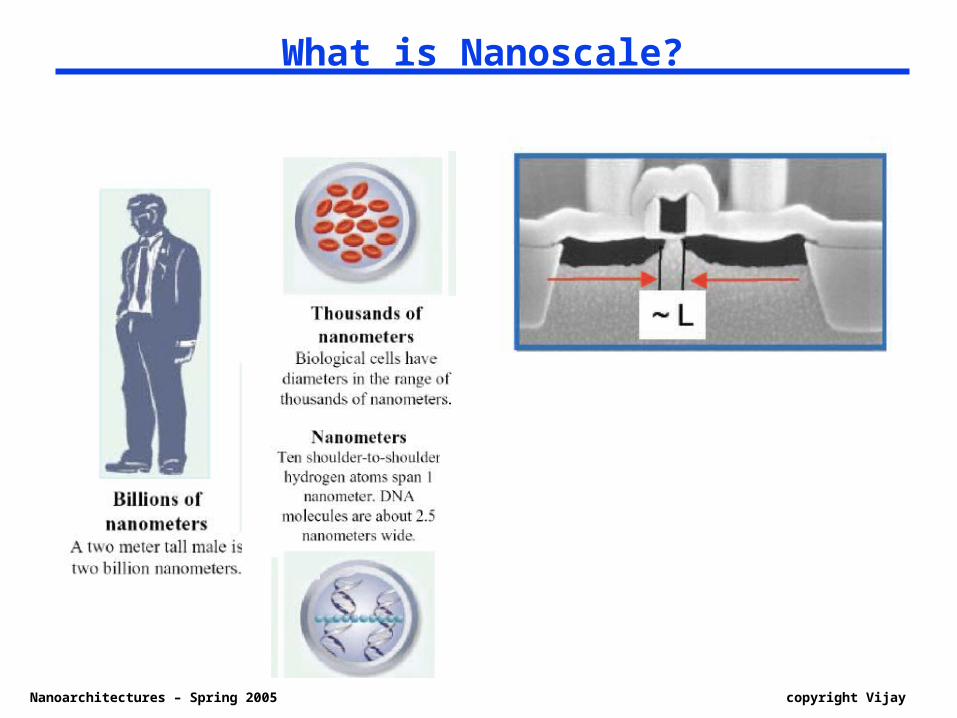
What is Nanoscale?
Nanoarchitectures – Spring 2005 copyright Vijay
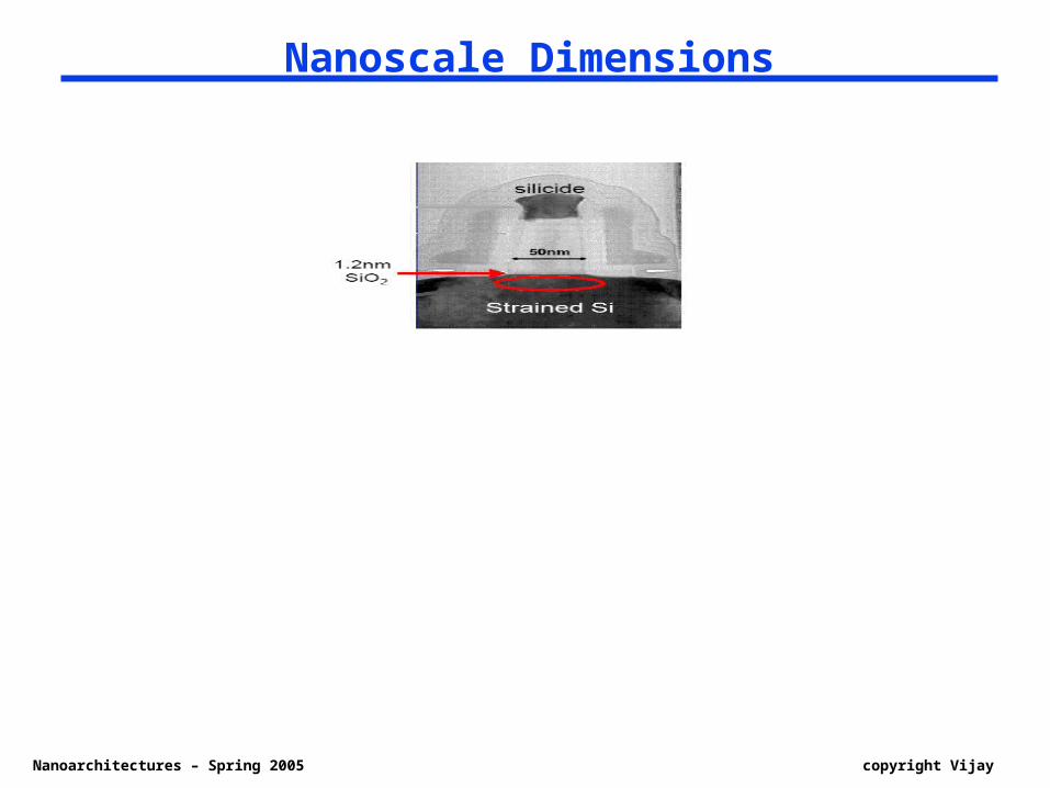
Nanoscale Dimensions
Nanoarchitectures – Spring 2005 copyright Vijay
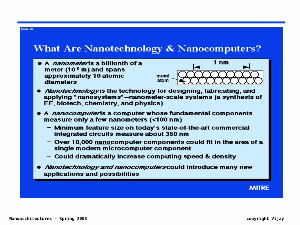
Nanoscale Properties A characteristic feature of moving to the
nanometer scale (besides the growing domination of quantum physical effects) is that properties of surfaces or boundary layers play an increasing role compared with the bulk properties of the material.
Basic structures of nanotechnology are: Pointlike structures smaller than 100 nm in all three
dimensions (e.g. nanocrystals, clusters or molecules) linear structures which are nanosized in two dimensions
(e.g. nanowires, nanotubes and nanogrooves) layered structures which are nanosized in only one
dimension, "inverse" nanostructures (i.e. pores) and complex structures such as supramolecular units or dendrimers.
Nanoarchitectures – Spring 2005 copyright Vijay
Nanoscale properties The reduction of size into the nanometer area
often results in characteristic properties of substances and materials which can be exploited for new applications and which do not appear in macroscopic pieces of the same materials.
significantly higher hardness and breaking strength superplasticity at high temperatures the emergence of additional electronic states high chemical selectivity of surface sites significantly increased surface energy
Nanoarchitectures – Spring 2005 copyright Vijay
How to achieve Nanoscale Features?
There are two fundamental strategies for penetrating the nanodimension.
"top-down" approach, which is predominant particularly in physics and physical technology.
Here,starting from microtechnology structures and components are more and more miniaturised.
"bottom-up/self-assembly" approach in which increasingly complex structures are specifically assembled from atomic or molecular components.
This approach is primarily featured in chemistry and biology, where dealing with objects of the nanometer scale has long been familiar practice.
Nanoarchitectures – Spring 2005 copyright Vijay
Interdisciplinary by Nature Nanotechnology requires a high degree of
interdisciplinary and transdisciplinary cooperation and communication. This is due to the fact that at the nano level the terminology of physics, chemistry and biology overlaps and blurs, and also to the fact that techniques from a single discipline can or must be supplemented by techniques and expertise from other disciplines.
Nanoarchitectures – Spring 2005 copyright Vijay
Nanoarchitectures – Spring 2005 copyright Vijay
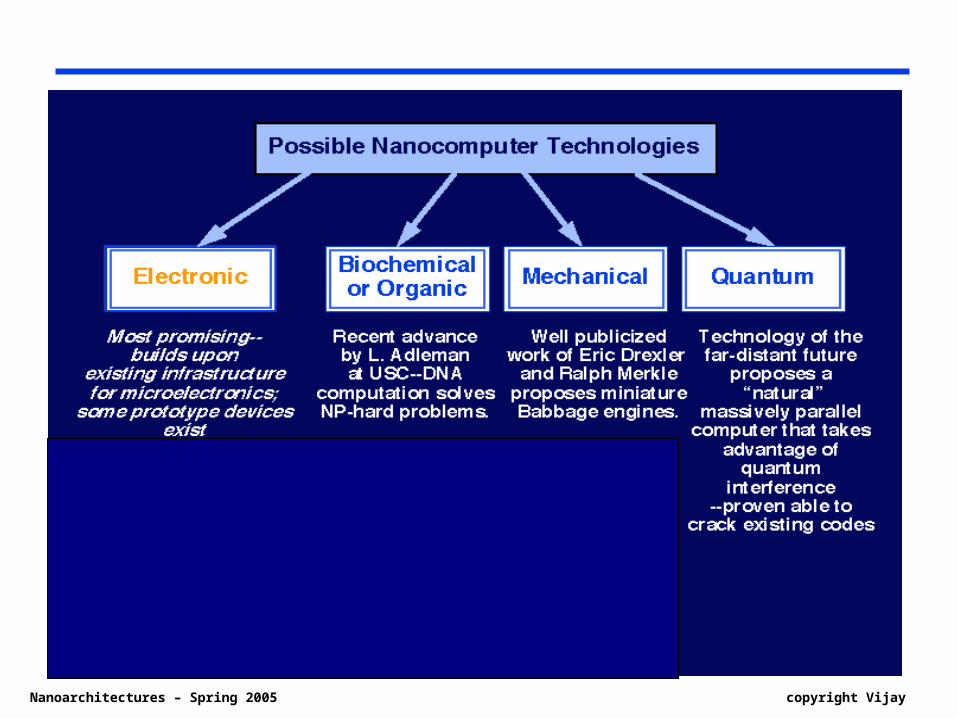
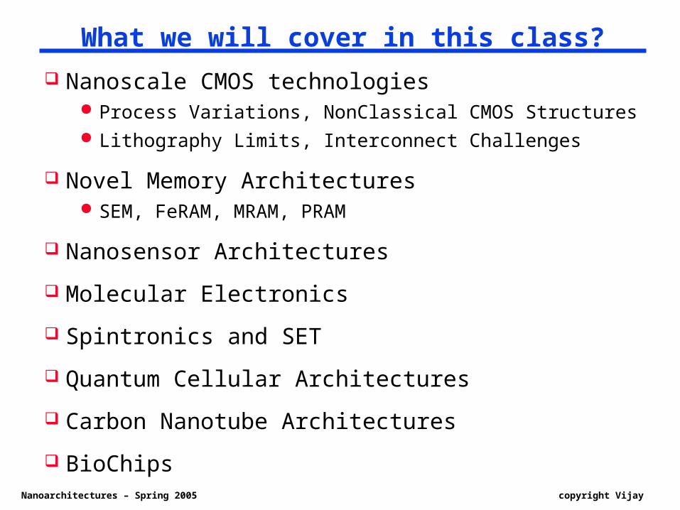
What we will cover in this class? Nanoscale CMOS technologies
Process Variations, NonClassical CMOS Structures Lithography Limits, Interconnect Challenges
Novel Memory Architectures SEM, FeRAM, MRAM, PRAM
Nanosensor Architectures
Molecular Electronics
Spintronics and SET
Quantum Cellular Architectures
Carbon Nanotube Architectures
BioChips
Nanoarchitectures – Spring 2005 copyright Vijay
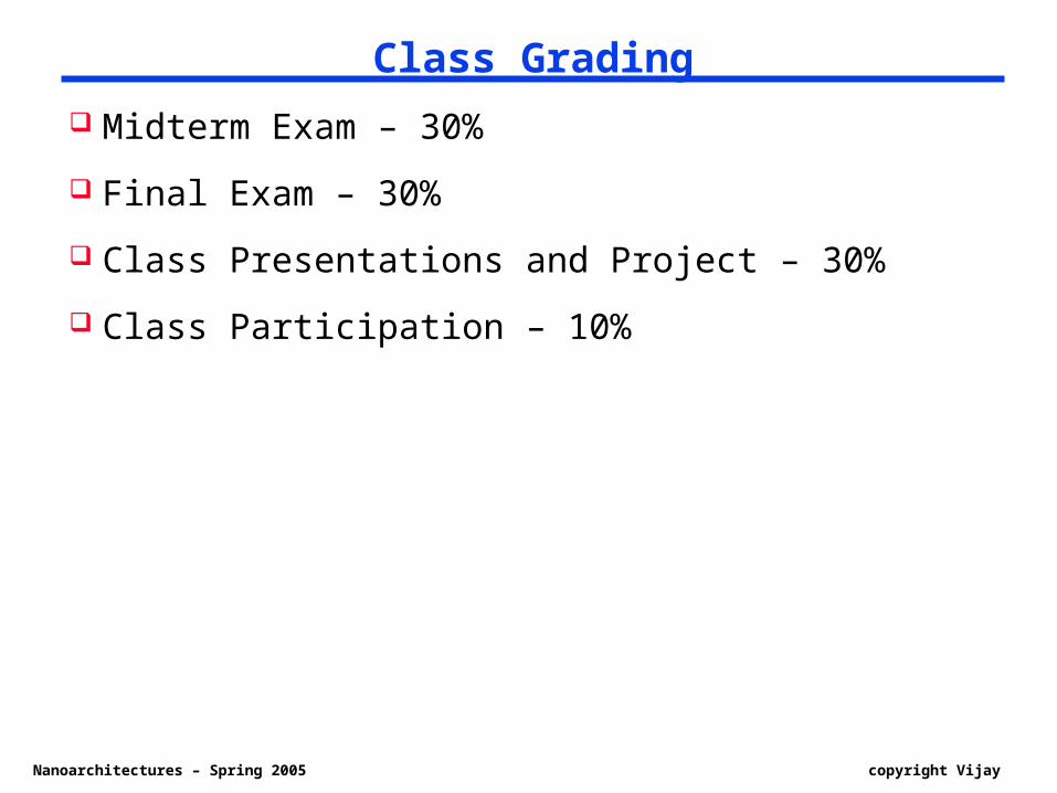
Class Grading Midterm Exam – 30%
Final Exam – 30%
Class Presentations and Project – 30%
Class Participation – 10%
Nanoarchitectures – Spring 2005 copyright Vijay
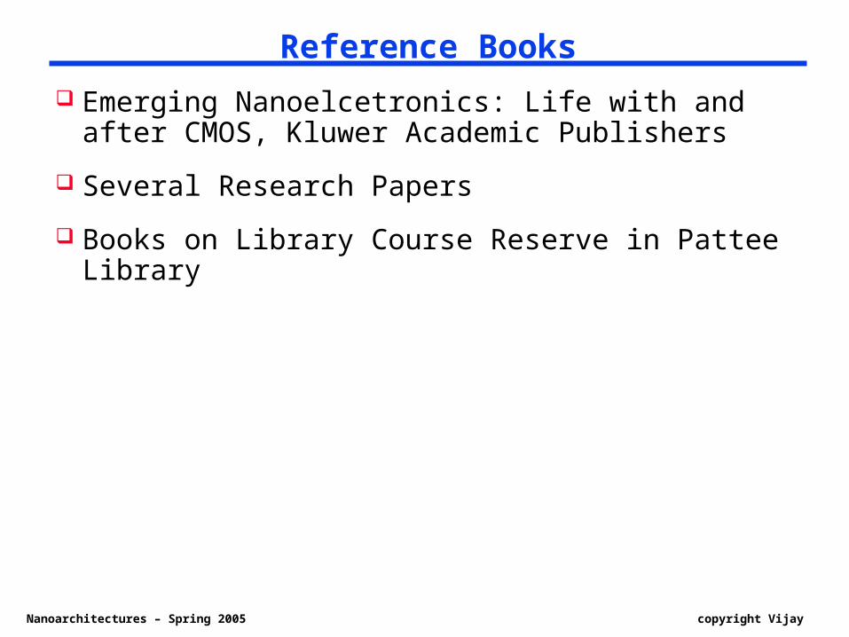
Reference Books Emerging Nanoelcetronics: Life with and after
CMOS, Kluwer Academic Publishers
Several Research Papers
Books on Library Course Reserve in Pattee Library
Nanoarchitectures – Spring 2005 copyright Vijay
CSE 598 Nanoarchitectures
Spring 2005
Lecture 2: Top 10 ChallengesVijay Narayanan (www.cse.psu.edu/~vijay)
Nanoarchitectures – Spring 2005 copyright Vijay
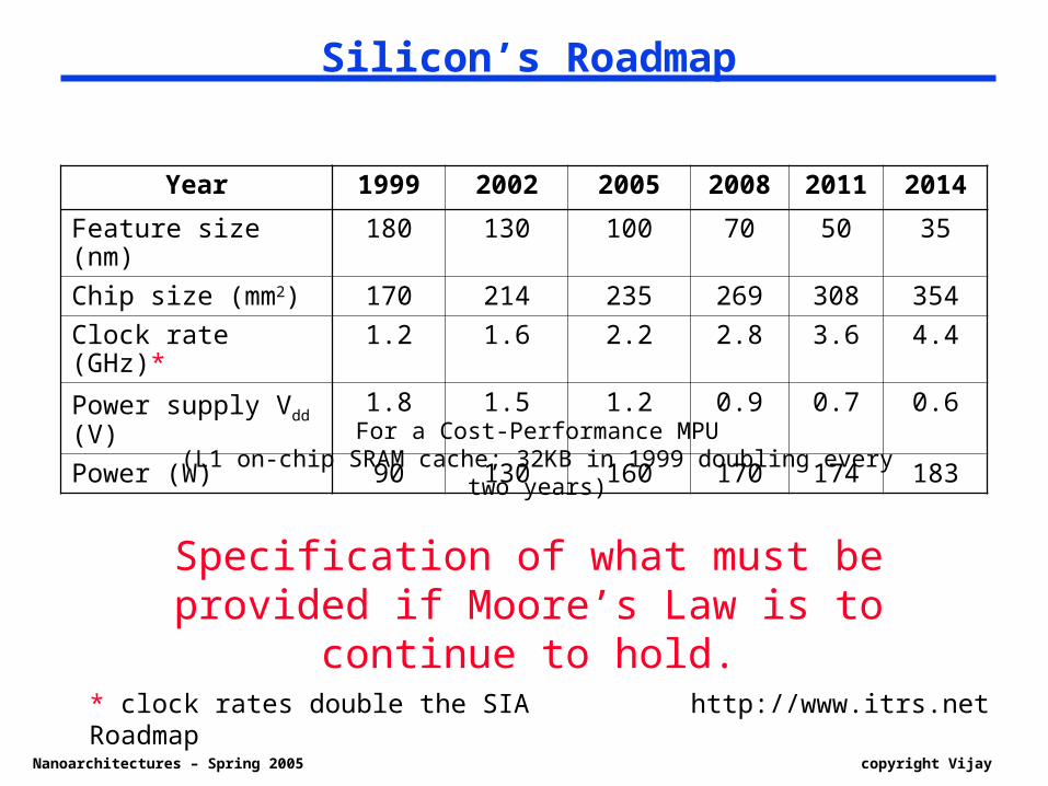
Silicon’s Roadmap
Year 1999 2002 2005 2008 2011 2014
Feature size (nm) 180 130 100 70 50 35
Chip size (mm2) 170 214 235 269 308 354
Clock rate (GHz)* 1.2 1.6 2.2 2.8 3.6 4.4
Power supply Vdd
(V)1.8 1.5 1.2 0.9 0.7 0.6
Power (W) 90 130 160 170 174 183For a Cost-Performance MPU
(L1 on-chip SRAM cache; 32KB in 1999 doubling every two years)
http://www.itrs.net
Specification of what must be provided if Moore’s Law is to
continue to hold.* clock rates double the SIA Roadmap
Nanoarchitectures – Spring 2005 copyright Vijay
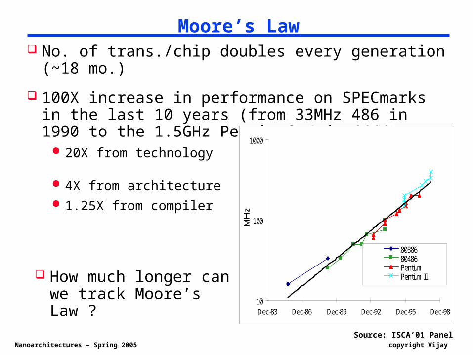
Moore’s Law No. of trans./chip doubles every generation (~18
mo.)
100X increase in performance on SPECmarks in the last 10 years (from 33MHz 486 in 1990 to the 1.5GHz Pentium 4 in 2000)
20X from technology scaling
4X from architecture 1.25X from compiler
technology
10
100
1000
Dec-83 Dec-86 Dec-89 Dec-92 Dec-95 Dec-98
8038680486PentiumPentium II
Expon.
How much longer can we track Moore’s Law ?
Source: ISCA’01 Panel
Nanoarchitectures – Spring 2005 copyright Vijay
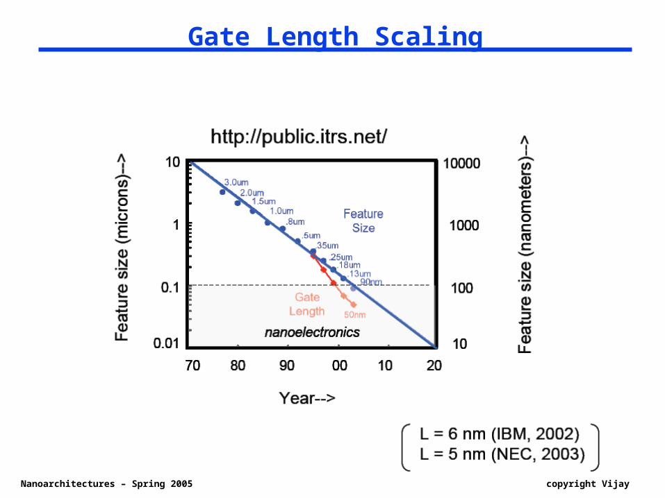
Gate Length Scaling
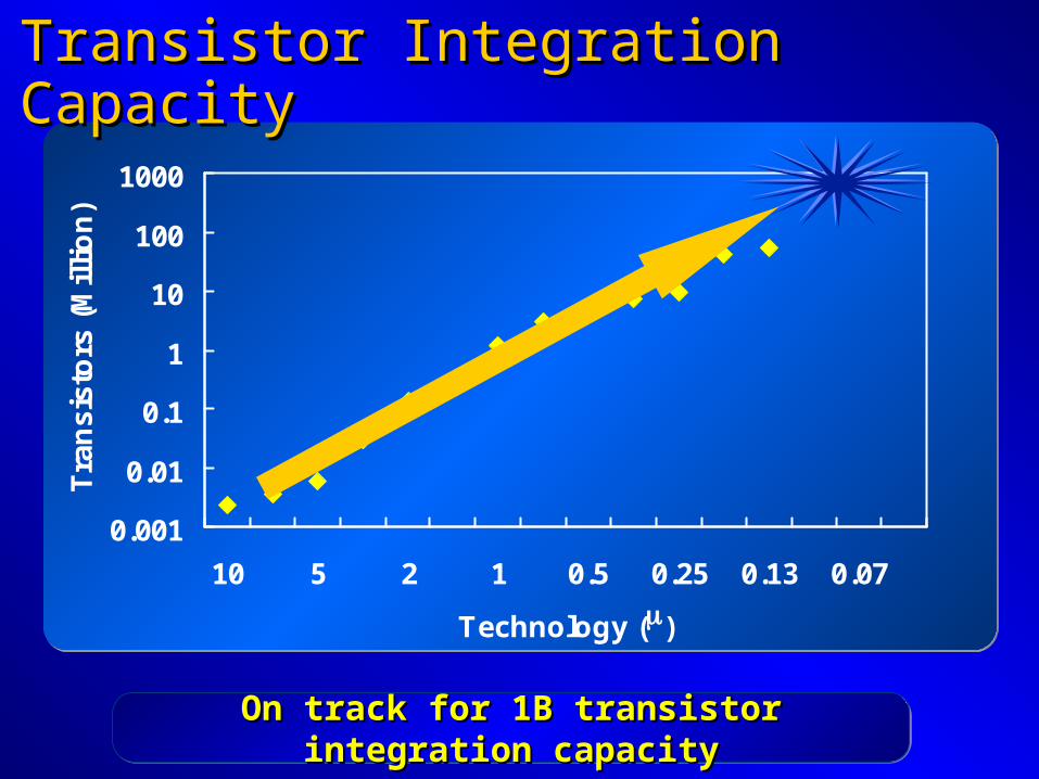
Transistor Integration CapacityTransistor Integration Capacity
0.001
0.01
0.1
1
10
100
1000
10 5 2 1 0.5 0.25 0.13 0.07
Technology (m)
Tra
nsi
sto
rs (
Mil
lio
n)
1 Billion
On track for 1B transistor integration capacityOn track for 1B transistor integration capacityOn track for 1B transistor integration capacityOn track for 1B transistor integration capacity
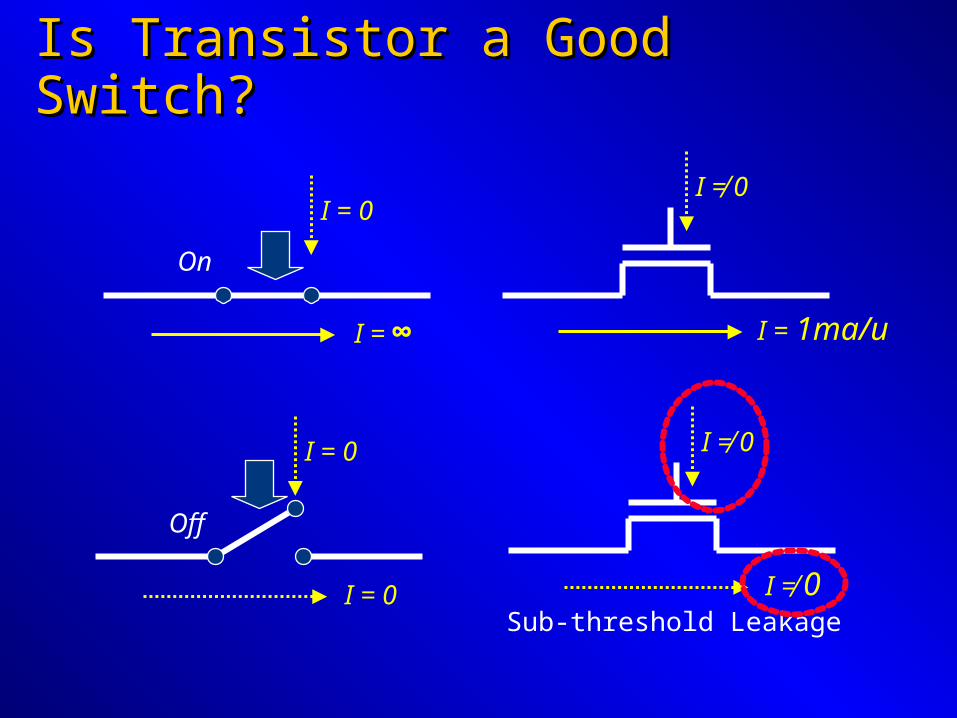
Is Transistor a Good Switch?Is Transistor a Good Switch?
On
I = ∞
I = 0
Off
I = 0
I = 0
I ≠ 0
I = 1ma/u
I ≠ 0
I ≠ 0Sub-threshold Leakage
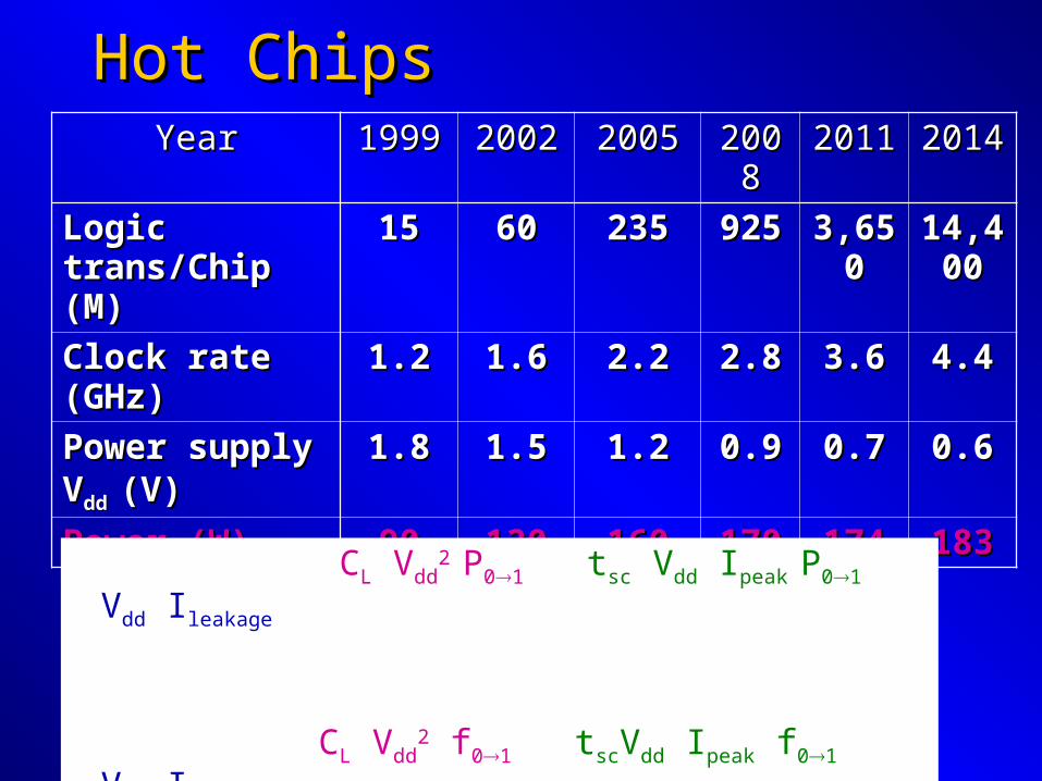
Hot ChipsHot Chips
Why worry about power consumption ? determines battery life for mobile units and . . .
YearYear 19991999 20022002 20052005 20082008 20112011 20142014
Logic Logic trans/Chip (M)trans/Chip (M)
1515 6060 235235 925925 3,6503,650 14,4014,4000
Clock rate Clock rate (GHz)(GHz)
1.21.2 1.61.6 2.22.2 2.82.8 3.63.6 4.44.4
Power supply Power supply VVdd dd (V)(V)
1.81.8 1.51.5 1.21.2 0.90.9 0.70.7 0.60.6
Power (W)Power (W) 9090 130130 160160 170170 174174 183183
E (joules) = CL Vdd2 P01 + tsc Vdd Ipeak P01 + Vdd
Ileakage
P (watts) = CL Vdd2 f01 + tscVdd Ipeak f01 + Vdd Ileakage

Challenge #1Challenge #1
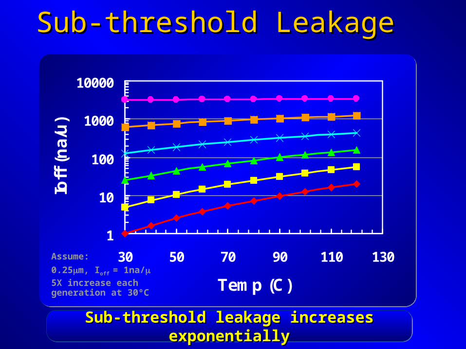
Sub-threshold LeakageSub-threshold Leakage
Sub-threshold leakage increases exponentiallySub-threshold leakage increases exponentiallySub-threshold leakage increases exponentiallySub-threshold leakage increases exponentially
1
10
100
1000
10000
30 50 70 90 110 130
Temp (C)
Ioff
(n
a/u
)
0.25u
45nm
Assume:
0.25mm, Ioff = 1na/m5X increase each generation at 30ºC
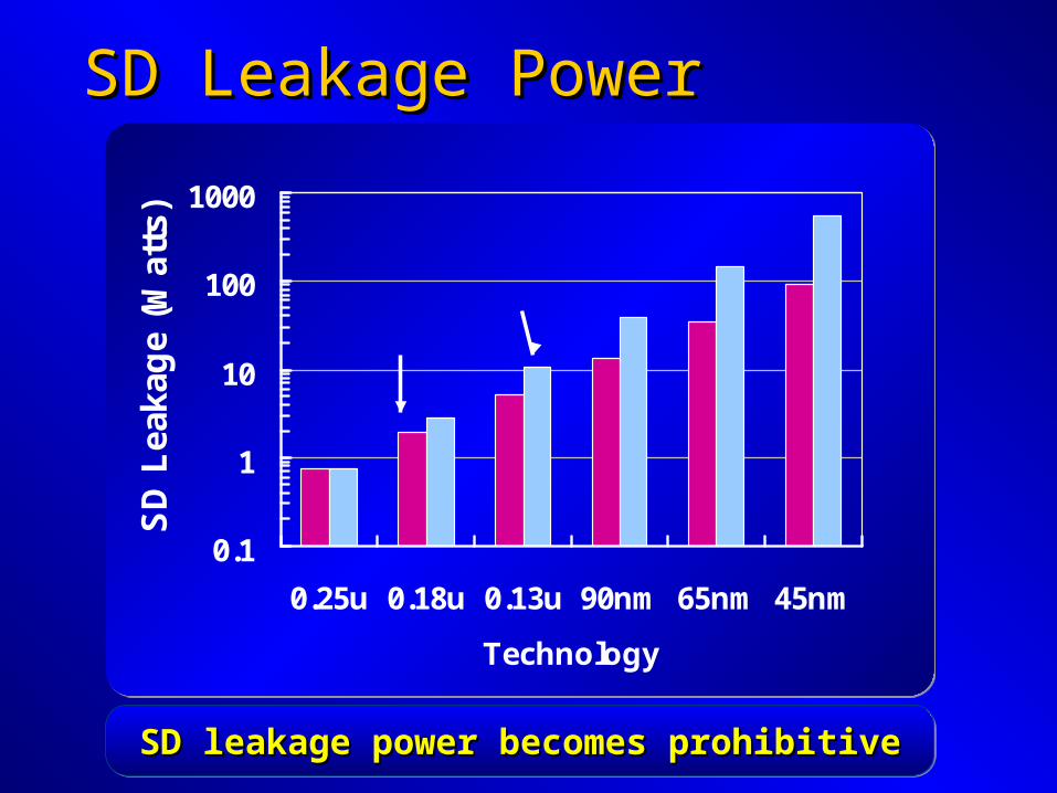
SD Leakage PowerSD Leakage Power
0.1
1
10
100
1000
0.25u 0.18u 0.13u 90nm 65nm 45nm
Technology
SD
Lea
kag
e (W
atts
)
2X Tr Growth1.5X Tr Growth
SD leakage power becomes prohibitiveSD leakage power becomes prohibitiveSD leakage power becomes prohibitiveSD leakage power becomes prohibitive
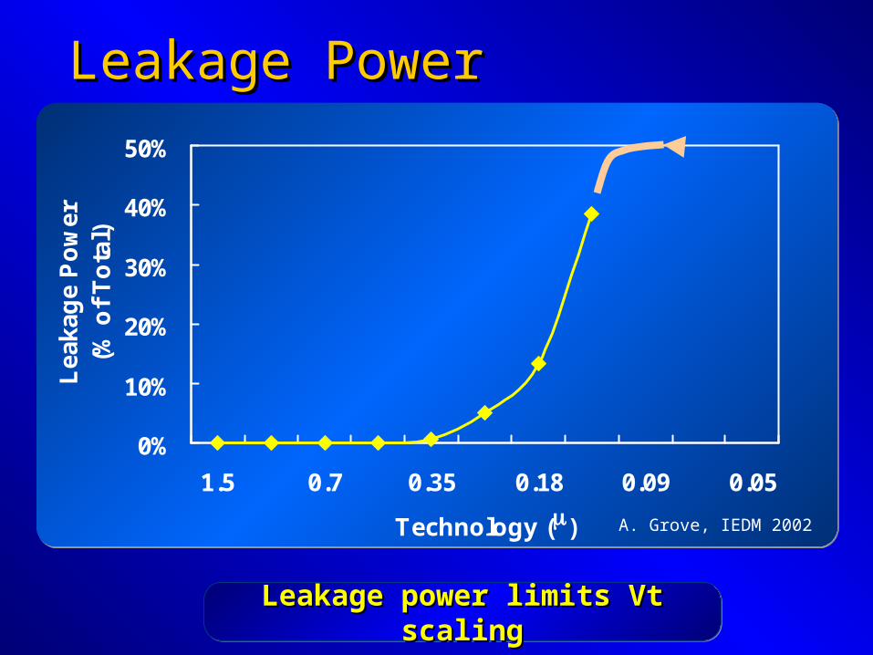
Leakage PowerLeakage Power
0%
10%
20%
30%
40%
50%
1.5 0.7 0.35 0.18 0.09 0.05
Technology (m)
Lea
kag
e P
ow
er(%
of
To
tal)
Must stopat 50%
Leakage power limits Vt scalingLeakage power limits Vt scalingLeakage power limits Vt scalingLeakage power limits Vt scaling
A. Grove, IEDM 2002

Challenge #2Challenge #2
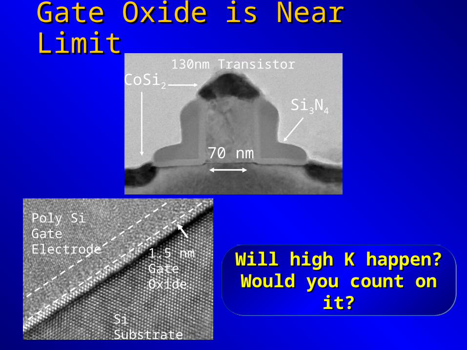
Gate Oxide is Near LimitGate Oxide is Near Limit
Poly Si Gate Electrode
Si Substrate
1.5 nm Gate Oxide
70 nm
Si3N4
CoSi2130nm Transistor
Will high K happen?Will high K happen?Would you count on it?Would you count on it?
Will high K happen?Will high K happen?Would you count on it?Would you count on it?
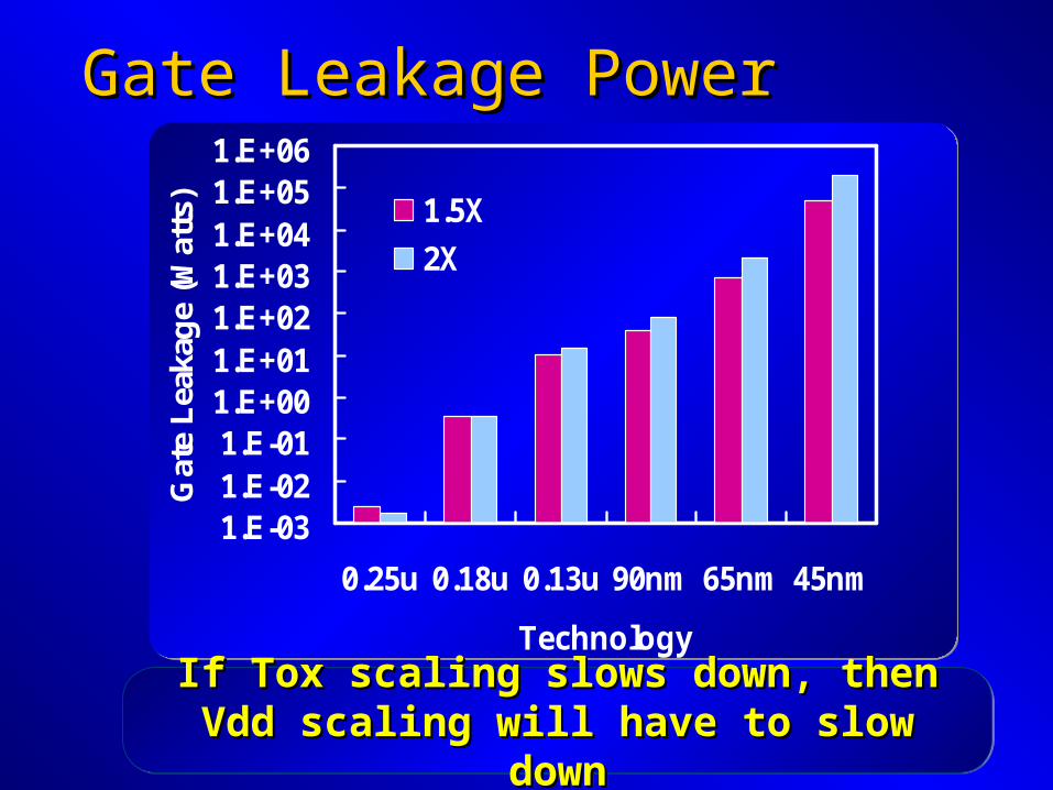
Gate Leakage PowerGate Leakage Power
1.E-031.E-021.E-011.E+001.E+011.E+021.E+031.E+041.E+051.E+06
0.25u 0.18u 0.13u 90nm 65nm 45nm
Technology
Gat
e L
eaka
ge
(Wat
ts)
1.5X
2X
During Burn-in1.4X Vdd
If Tox scaling slows down, then Vdd If Tox scaling slows down, then Vdd scaling will have to slow downscaling will have to slow down
If Tox scaling slows down, then Vdd If Tox scaling slows down, then Vdd scaling will have to slow downscaling will have to slow down
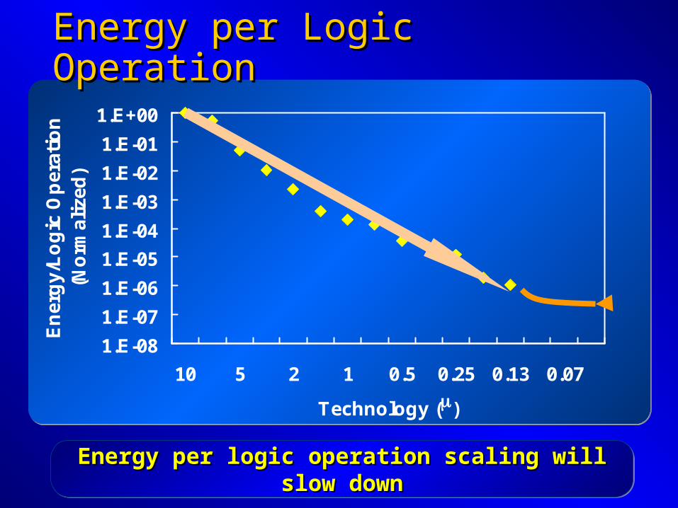
Energy per Logic OperationEnergy per Logic Operation
1.E-08
1.E-07
1.E-06
1.E-05
1.E-04
1.E-03
1.E-02
1.E-01
1.E+00
10 5 2 1 0.5 0.25 0.13 0.07
Technology (m)
En
erg
y/L
og
ic O
per
atio
n
(No
rmal
ized
)
This was Good
Slow down
Energy per logic operation scaling will slow downEnergy per logic operation scaling will slow downEnergy per logic operation scaling will slow downEnergy per logic operation scaling will slow down

Challenge #4Challenge #4
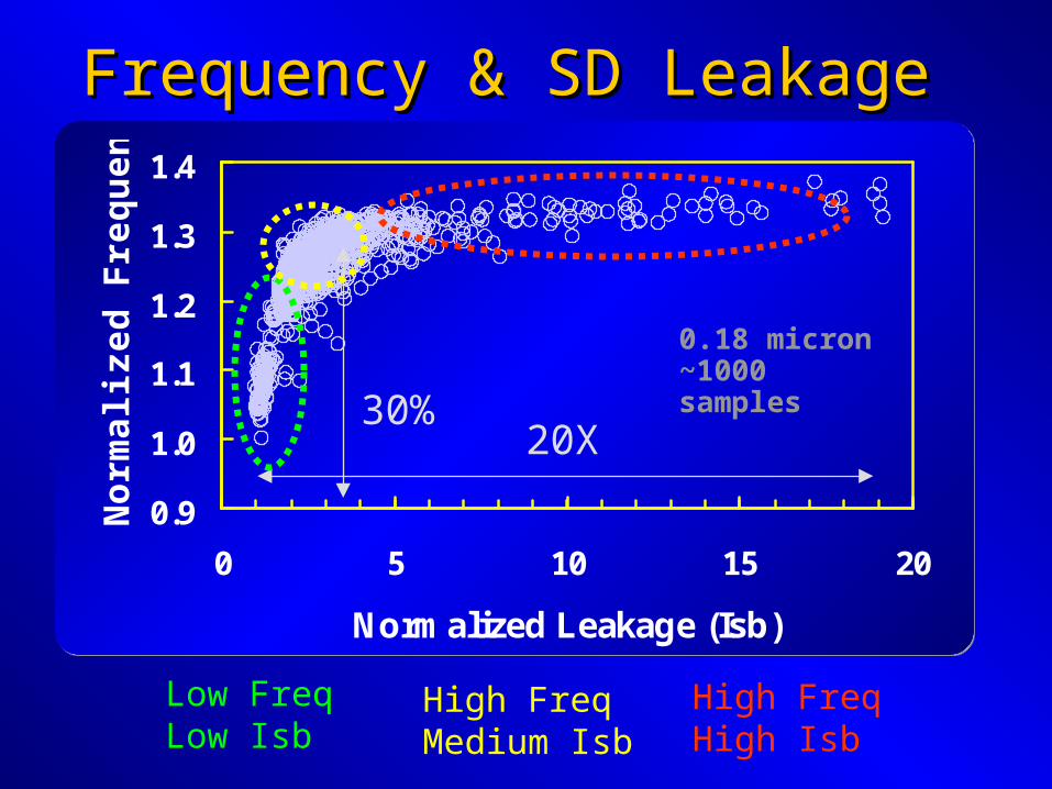
Frequency & SD LeakageFrequency & SD Leakage
0.9
1.0
1.1
1.2
1.3
1.4
0 5 10 15 20
Normalized Leakage (Isb)
No
rmal
ized
Fre
qu
ency
0.18 micron~1000 samples
20X30%
Low FreqLow Isb
High FreqMedium Isb
High FreqHigh Isb
0
20
40
60
80
100
120
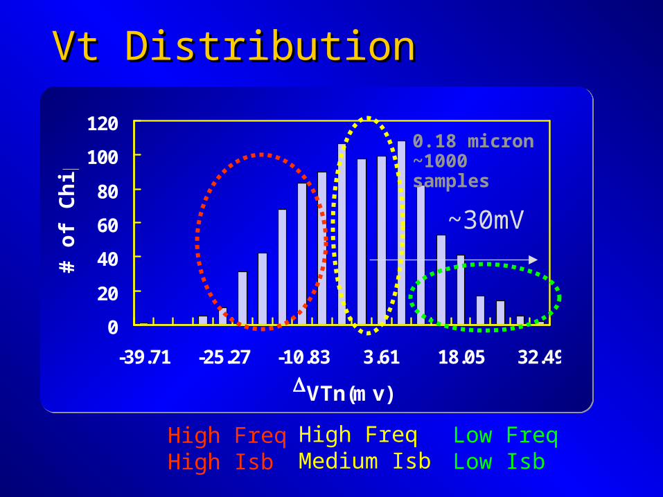
-39.71 -25.27 -10.83 3.61 18.05 32.49
VTn(mv)
# o
f C
hip
s
~30mV
Vt DistributionVt Distribution
0.18 micron~1000 samples
Low FreqLow Isb
High FreqMedium Isb
High FreqHigh Isb
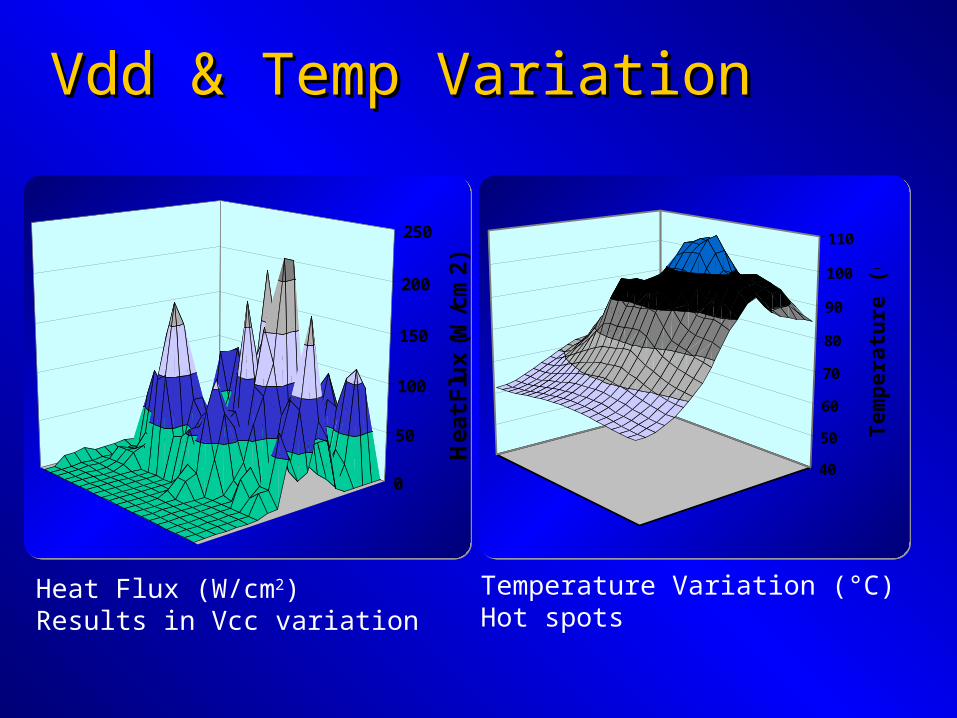
Vdd & Temp VariationVdd & Temp Variation
40
50
60
70
80
90
100
110
Tem
per
atu
re (
C)
0
50
100
150
200
250
He
at F
lux
(W
/cm
2)
Heat Flux (W/cm2)Results in Vcc variation
Temperature Variation (°C)Hot spots

Challenge #6Challenge #6
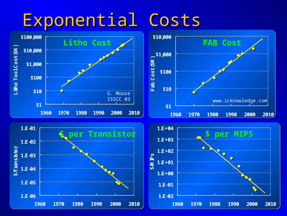
Exponential CostsExponential Costs
$1
$10
$100
$1,000
$10,000
$100,000
1960 1970 1980 1990 2000 2010
Lit
ho
To
ol
Co
st (
$K)
G. MooreISSCC 03
Litho Cost
$1
$10
$100
$1,000
$10,000
1960 1970 1980 1990 2000 2010
Fab
Co
st (
$M)
www.icknowledge.com
FAB Cost
1.E-06
1.E-05
1.E-04
1.E-03
1.E-02
1.E-01
1960 1970 1980 1990 2000 2010
$/T
ran
sist
or
$ per Transistor
1.E-02
1.E-01
1.E+00
1.E+01
1.E+02
1.E+03
1.E+04
1960 1970 1980 1990 2000 2010
$/M
IPs
$ per MIPS
Nanoarchitectures – Spring 2005 copyright Vijay
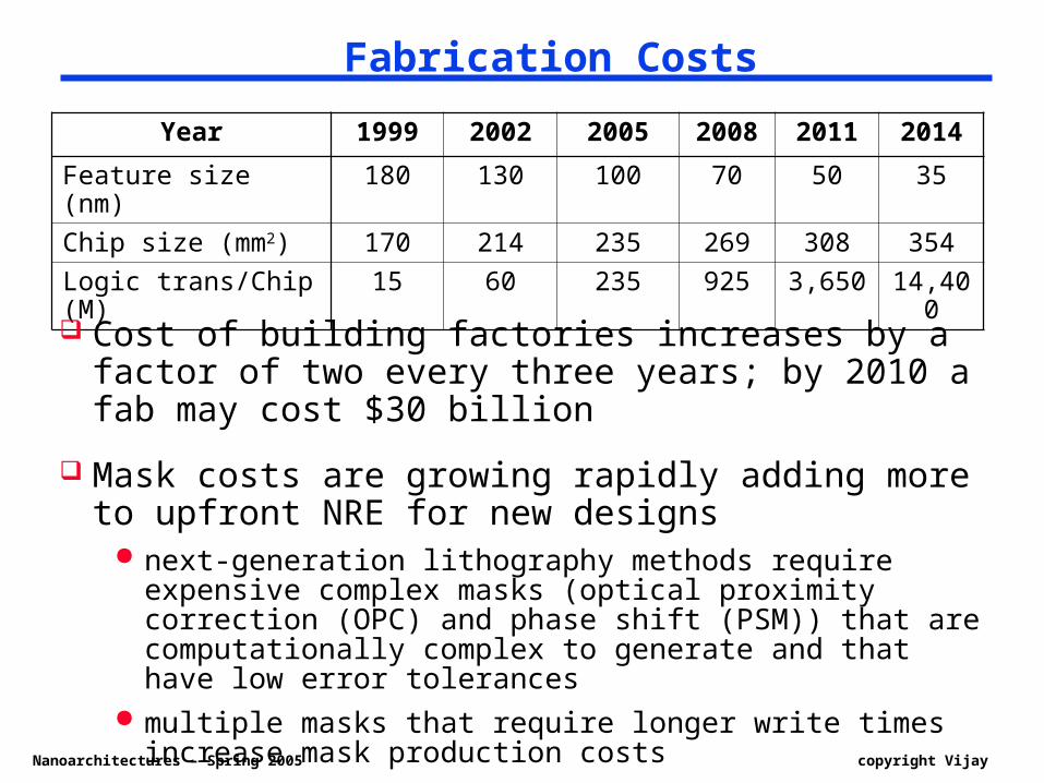
Fabrication Costs
Year 1999 2002 2005 2008 2011 2014
Feature size (nm) 180 130 100 70 50 35
Chip size (mm2) 170 214 235 269 308 354
Logic trans/Chip (M)
15 60 235 925 3,650 14,400
Cost of building factories increases by a factor of two every three years; by 2010 a fab may cost $30 billion
Mask costs are growing rapidly adding more to upfront NRE for new designs
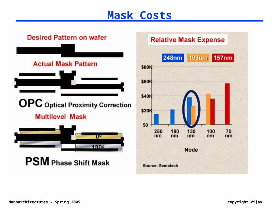
next-generation lithography methods require expensive complex masks (optical proximity correction (OPC) and phase shift (PSM)) that are computationally complex to generate and that have low error tolerances
multiple masks that require longer write times increase mask production costs
Nanoarchitectures – Spring 2005 copyright Vijay
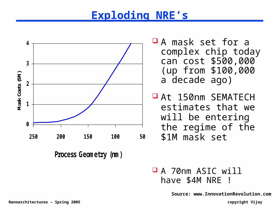
Exploding NRE’s
0
1
2
3
4
250 200 150 100 50
Process Geometry (nm)
Mas
k Co
sts
($M
)
A mask set for a complex chip today can cost $500,000 (up from $100,000 a decade ago)
At 150nm SEMATECH estimates that we will be entering the regime of the $1M mask set
A 70nm ASIC will have $4M NRE !
Source: www.InnovationRevolution.com
Nanoarchitectures – Spring 2005 copyright Vijay
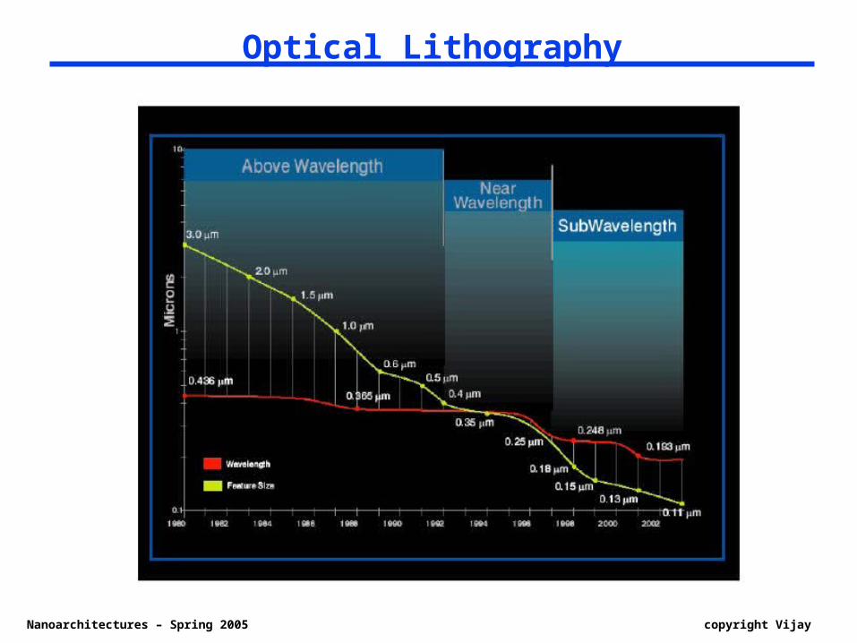
Optical Lithography
Nanoarchitectures – Spring 2005 copyright Vijay
Mask Costs
Nanoarchitectures – Spring 2005 copyright Vijay
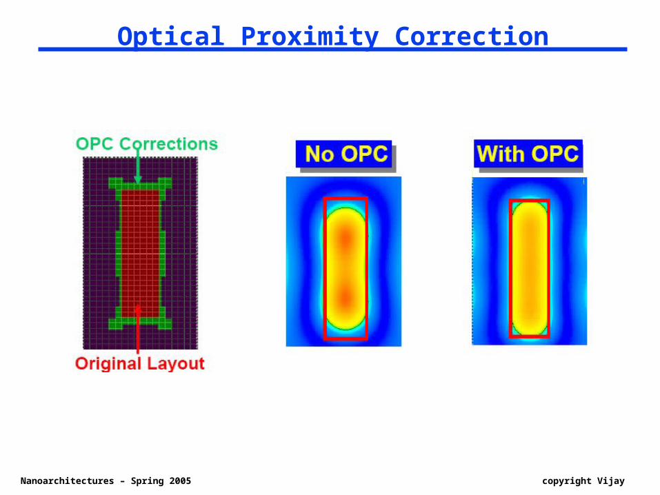
Optical Proximity Correction
Nanoarchitectures – Spring 2005 copyright Vijay
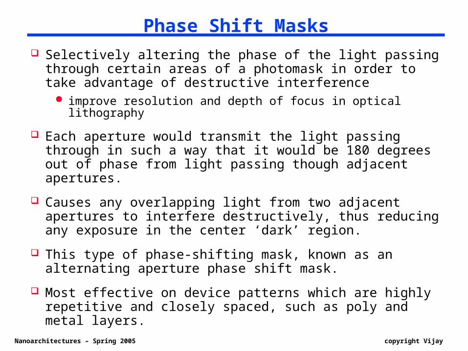
Phase Shift Masks Selectively altering the phase of the light passing through
certain areas of a photomask in order to take advantage of destructive interference
improve resolution and depth of focus in optical lithography
Each aperture would transmit the light passing through in such a way that it would be 180 degrees out of phase from light passing though adjacent apertures.
Causes any overlapping light from two adjacent apertures to interfere destructively, thus reducing any exposure in the center ‘dark’ region.
This type of phase-shifting mask, known as an alternating aperture phase shift mask.
Most effective on device patterns which are highly repetitive and closely spaced, such as poly and metal layers.
Nanoarchitectures – Spring 2005 copyright Vijay
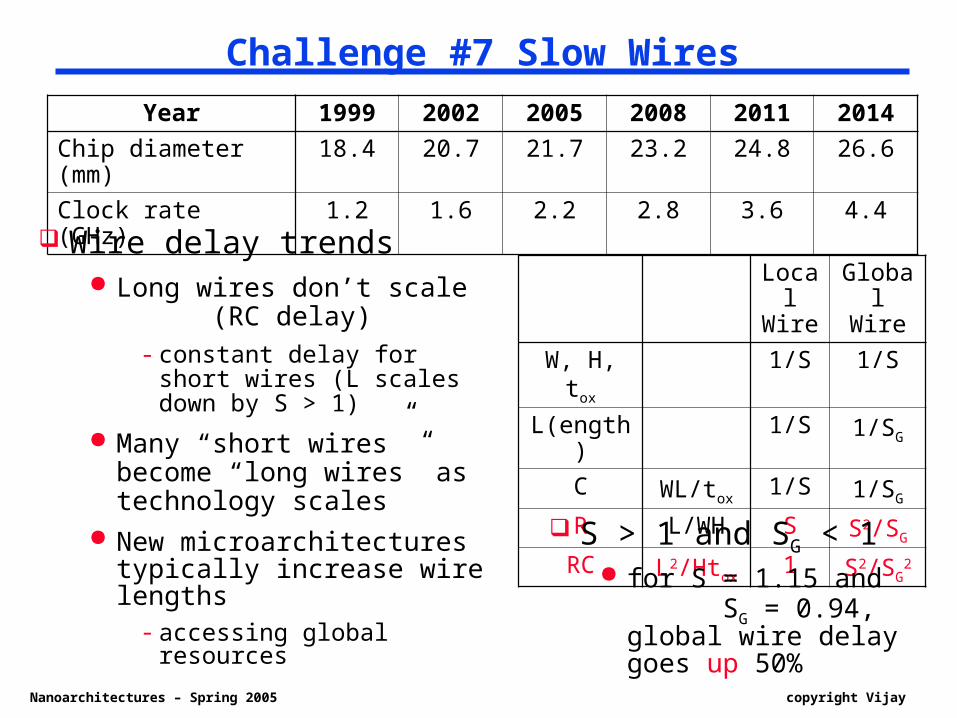
Challenge #7 Slow Wires
Year 1999 2002 2005 2008 2011 2014
Chip diameter (mm)
18.4 20.7 21.7 23.2 24.8 26.6
Clock rate (GHz) 1.2 1.6 2.2 2.8 3.6 4.4 Wire delay trends
Long wires don’t scale (RC delay)
- constant delay for short wires (L scales down by S > 1)
Many “short wires” become “long wires” as technology scales
New microarchitectures typically increase wire lengths- accessing global resources
Local
Wire
Global Wire
W, H, tox1/S 1/S
L(ength) 1/S 1/SG
C WL/tox1/S 1/SG
R L/WH S S2/SG
RC L2/Htox1 S2/SG
2 S > 1 and SG < 1
for S = 1.15 and SG = 0.94, global wire delay goes up 50%
Nanoarchitectures – Spring 2005 copyright Vijay
0
0.2
0.4
0.6
250 180 130 100
70 50 35
pF
Technology Ldrawn (nm)
Semi-local wire capacitance, scaled length
Aggressive scalingConservative scaling
0
0.1
0.2
0.3
0.4
250 180 130 100 70 50 35
Kohm
s
Technology Ldrawn (nm)
Semi-local wire resistance, scaled length
Aggressive scalingConservative scaling
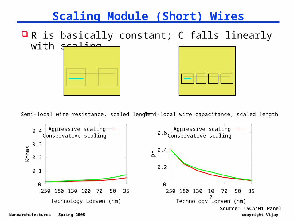
Scaling Module (Short) Wires R is basically constant; C falls linearly with scaling
Source: ISCA’01 Panel
Nanoarchitectures – Spring 2005 copyright Vijay
0
0.2
0.4
0.6
250 180 130 100 70 50 35
pF
Technology Ldrawn (nm)
Semi-global wire capacitance, 1mm long
Aggressive scalingConservative scaling
0
0.1
0.2
0.3
0.4
0.25 0.18 0.13 0.1 0.07 50 35
Kohm
s
Technology Ldrawn (nm)
Semi-global wire resistance, 1mm long
Aggressive scalingConservative scaling
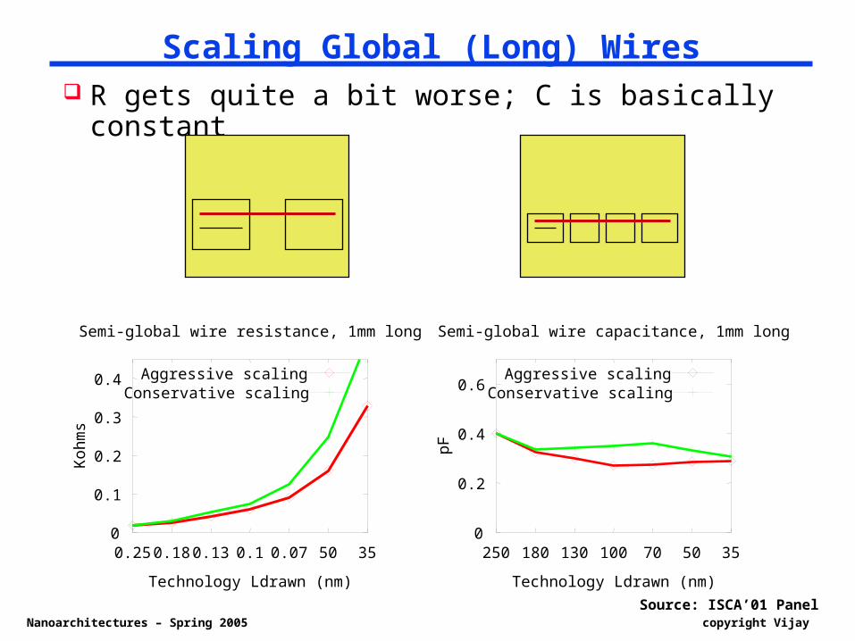
Scaling Global (Long) Wires R gets quite a bit worse; C is basically constant
Source: ISCA’01 Panel
Nanoarchitectures – Spring 2005 copyright Vijay
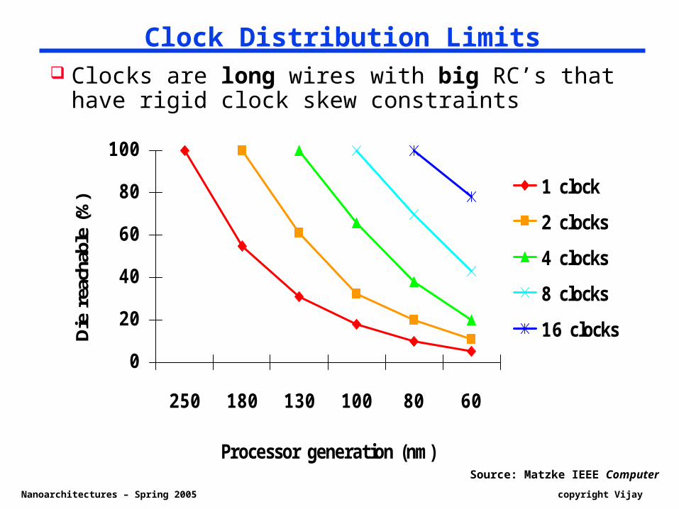
Clock Distribution Limits
0
20
40
60
80
100
250 180 130 100 80 60
Processor generation (nm)
Die
rea
chab
le (
%) 1 clock
2 clocks
4 clocks
8 clocks
16 clocks
Source: Matzke IEEE Computer
Clocks are long wires with big RC’s that have rigid clock skew constraints
Nanoarchitectures – Spring 2005 copyright Vijay
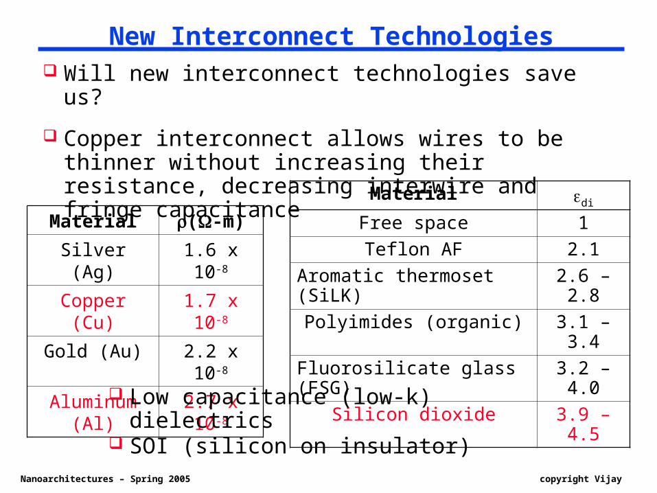
New Interconnect Technologies Will new interconnect technologies save us?
Copper interconnect allows wires to be thinner without increasing their resistance, decreasing interwire and fringe capacitance
Material (-m)
Silver (Ag) 1.6 x 10⁻⁸
Copper (Cu) 1.7 x 10⁻⁸
Gold (Au) 2.2 x 10⁻⁸
Aluminum (Al)
2.7 x 10⁻⁸
Material di
Free space 1Teflon AF 2.1
Aromatic thermoset (SiLK)
2.6 – 2.8
Polyimides (organic) 3.1 – 3.4Fluorosilicate glass (FSG) 3.2 – 4.0
Silicon dioxide 3.9 – 4.5 Low capacitance (low-k) dielectrics
SOI (silicon on insulator)
Nanoarchitectures – Spring 2005 copyright Vijay
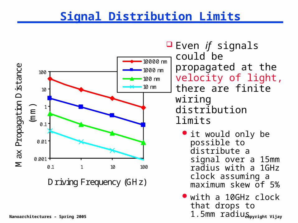
Signal Distribution Limits
0.001
0.01
0.1
1
10
100
0.1 1 10 100
Driving Frequency (GHz)
Max
Pro
paga
tion
Dis
tanc
e
(mm
)
10000 nm
1000 nm
100 nm10 nm
Even if signals could be propagated at the velocity of light, there are finite wiring distribution limits
it would only be possible to distribute a signal over a 15mm radius with a 1GHz clock assuming a maximum skew of 5%
with a 10GHz clock that drops to 1.5mm radius
Nanoarchitectures – Spring 2005 copyright Vijay
Challenge #8 Chip I/O Bottleneck
Limited signal pins consume large number of
pins in power/ground supplies (to combat the supply rail bounce)
what happens to Rent’s Rule ?
Year 1999 2002 2005 2008 2011 2014
Logic trans/chip (M)
15 60 235 925 3,650 14,400
Signal pins/chip 768 1024 1024 1280 1408 1472
1
10
100
1000
10000
1999 2002 2005 2008 2011 2014
Year
Logi
c tr
ans/
Sig
nal
pins
T = t Bp
0 p 1 Rent exponent
Normal values: 0.5 p 0.75
t average # pins/block
T = # signal pins/chip
Source: Landman, Russo, IEEETC, 1971
Nanoarchitectures – Spring 2005 copyright Vijay
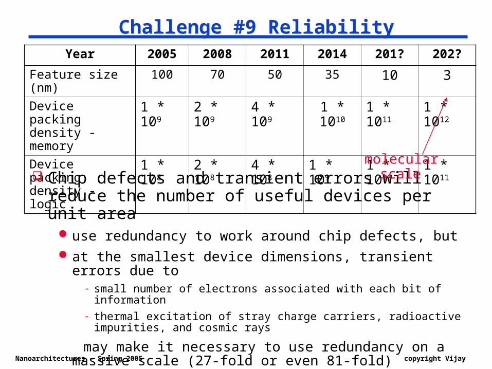
Challenge #9 ReliabilityYear 2005 2008 2011 2014 201? 202?
Feature size (nm)
100 70 50 35 10 3
Device packing density - memory
1 * 109
2 * 109 4 * 109 1 * 1010
1 * 1011
1 * 1012
Device packing density - logic
1 * 108
2 * 108 4 * 108 1 * 109 1 * 1010
1 * 1011
Chip defects and transient errors will reduce the number of useful devices per unit area
use redundancy to work around chip defects, but at the smallest device dimensions, transient errors due
to- small number of electrons associated with each bit of information- thermal excitation of stray charge carriers, radioactive impurities,
and cosmic rays
may make it necessary to use redundancy on a massive scale (27-fold or even 81-fold)
Thermal densities will aggravate transient errors
molecular scale
Nanoarchitectures – Spring 2005 copyright Vijay
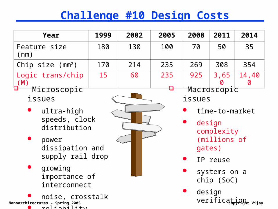
Challenge #10 Design Costs
Year 1999 2002 2005 2008 2011 2014
Feature size (nm) 180 130 100 70 50 35
Chip size (mm2) 170 214 235 269 308 354
Logic trans/chip (M)
15 60 235 925 3,650
14,400
Microscopic issues ultra-high speeds,
clock distribution
power dissipation and supply rail drop
growing importance of interconnect
noise, crosstalk
reliability, manufacturability
Macroscopic issues time-to-market
design complexity (millions of gates)
IP reuse
systems on a chip (SoC)
design verification
tool interoperability
Nanoarchitectures – Spring 2005 copyright Vijay
0.0010.01
0.11
10100
100010000
1981
1983
1985
1987
1989
1993
1995
1997
1999
2001
2003
2005
2007
2009
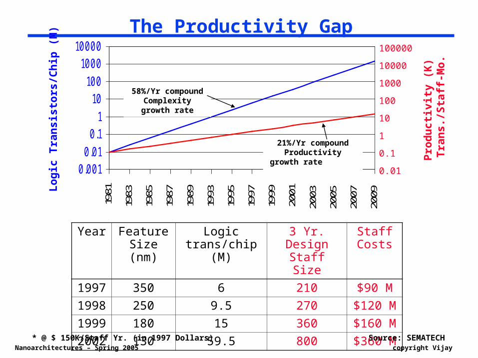
58%/Yr compoundComplexity growth rate
The Productivity Gap
Year Feature Size (nm)
Logic trans/chip
(M)
3 Yr. Design
Staff Size
Staff Costs
1997 350 6 210 $90 M
1998 250 9.5 270 $120 M
1999 180 15 360 $160 M
2002 130 59.5 800 $360 M* @ $ 150K/Staff Yr. (in 1997 Dollars) Source: SEMATECH
21%/Yr compoundProductivity growth rate
100000
10000
1000
100
10
1
0.1
0.01
Log
ic T
ran
sis
tors
/Ch
ip (
M)
Pro
du
cti
vit
y (
K)
Tra
ns./
Sta
ff-M
o.
Nanoarchitectures – Spring 2005 copyright Vijay
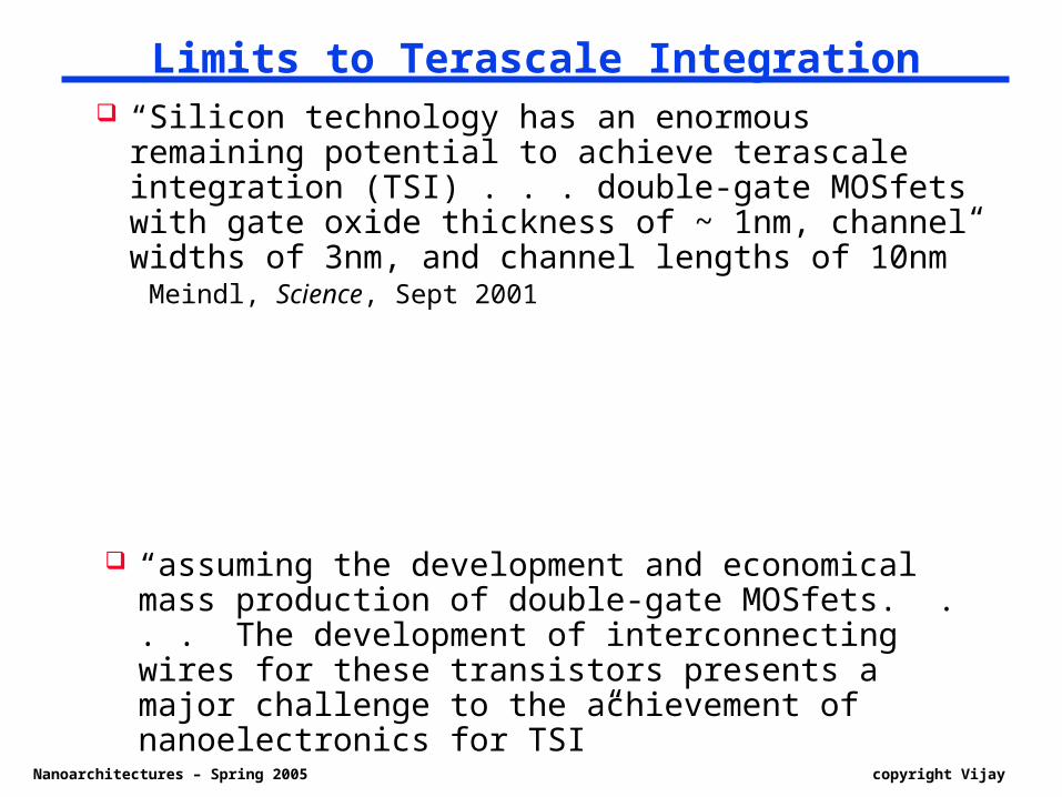
Limits to Terascale Integration “Silicon technology has an enormous remaining
potential to achieve terascale integration (TSI) . . . double-gate MOSfets with gate oxide thickness of ~ 1nm, channel widths of 3nm, and channel lengths of 10nm” Meindl, Science, Sept 2001
“assuming the development and economical mass production of double-gate MOSfets. . . . The development of interconnecting wires for these transistors presents a major challenge to the achievement of nanoelectronics for TSI”
Nanoarchitectures – Spring 2005 copyright Vijay
Hybrid Technologies Nanotechnology may offer solutions to some of the issues with
future scaling of CMOS technology.
Global on-chip metal wires may be replaced with strategically located strapped on nanotubes
I/O pads may be largely replaced with nanotech/MEMS sensors and actuators (chips that see, smell, hear, taste)
low power nanotech alternatives for wireless communication components will emerge
radically new high density, nonvolatile, on-chip storage technologies
are already on the horizon.
Use of nanotechnology may help to
mitigate power consumption
reduce mask costs (due to the use of technologies that self assemble).
Nanoarchitectures – Spring 2005 copyright Vijay
Nano-overview Reading
The Future of Nanocomputing, Computer Aug 2003, pp 44-.
Nanoarchitectures – Spring 2005 copyright Vijay
CSE 598 NanoarchitecturesSpring 2005
Lecture 3: Future of Nanocomputing
Vijay Narayanan (www.cse.psu.edu/~vijay)
Nanoarchitectures – Spring 2005 copyright Vijay
The Future of Nanocomputing – Looking Back
Bandstructure Concept
Effect of impurities on semiconductor properties
Advances in producing high-quality crystal interfaces in silicon and germanium
Devices 1948 – bipolar transistors 1953 – FET 1955 – LED 1957 – Tunnel Diodes 1959 – ICs 1962 – Semiconductor lasers
Nanoarchitectures – Spring 2005 copyright Vijay
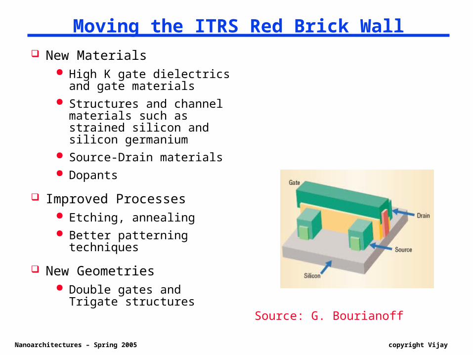
Moving the ITRS Red Brick Wall New Materials
High K gate dielectrics and gate materials
Structures and channel materials such as strained silicon and silicon germanium
Source-Drain materials Dopants
Improved Processes Etching, annealing Better patterning
techniques
New Geometries Double gates and Trigate
structuresSource: G. Bourianoff
Nanoarchitectures – Spring 2005 copyright Vijay
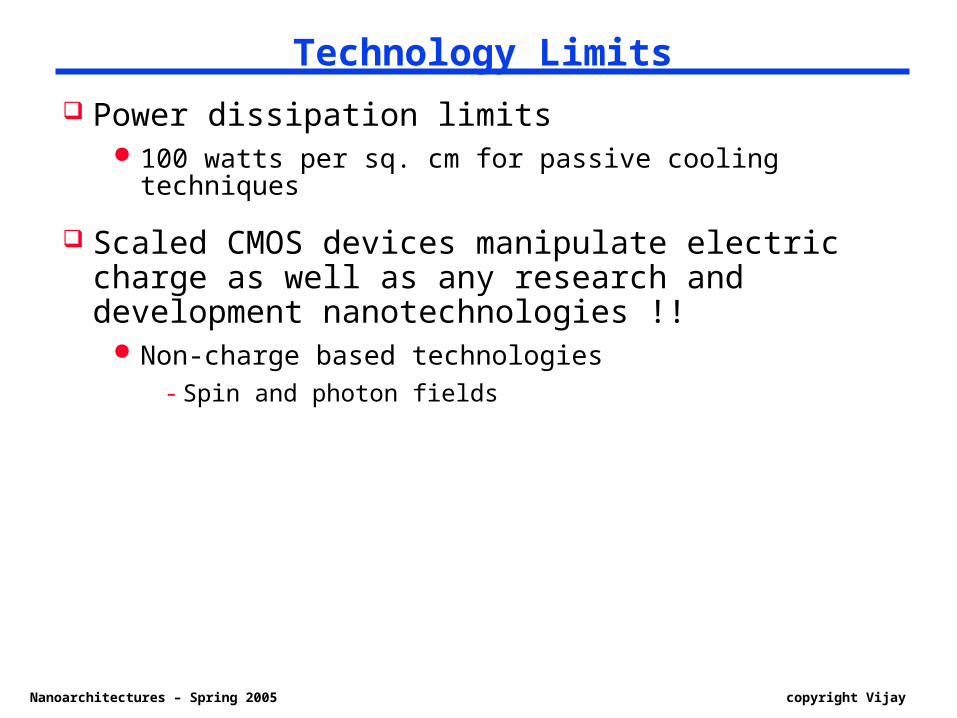
Technology Limits Power dissipation limits
100 watts per sq. cm for passive cooling techniques
Scaled CMOS devices manipulate electric charge as well as any research and development nanotechnologies !!
Non-charge based technologies- Spin and photon fields
Nanoarchitectures – Spring 2005 copyright Vijay
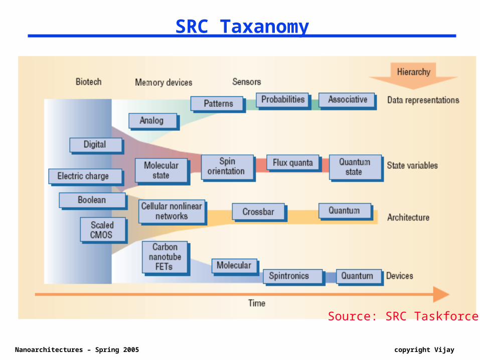
SRC Taxanomy
Source: SRC Taskforce
Nanoarchitectures – Spring 2005 copyright Vijay
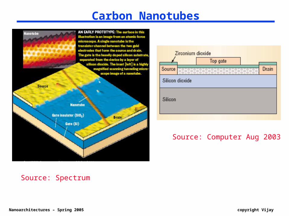
Carbon Nanotubes
Source: Spectrum
Source: Computer Aug 2003
Nanoarchitectures – Spring 2005 copyright Vijay
Carbon Nanotube To form carbon nanotubes, an atomic planar
sheet of carbon atoms is bonded together into an array of hexagons and rolled up to form molecular tubes or cylinders with 1 to 20 nm diameters and ranging from 100 nm to several microns in length.
The subthreshold slope of 70 mV per decade for the p-type transistors approaches the room-temperature theoretical limit of 60 mV.
Subthreshold swing is a key parameter for transistor miniaturization since it measures how well a small swing in gate voltage can cut off current flow.
Low cutoff current directly translates into low standby power—a major challenge for end-of the Roadmap devices.
Nanoarchitectures – Spring 2005 copyright Vijay
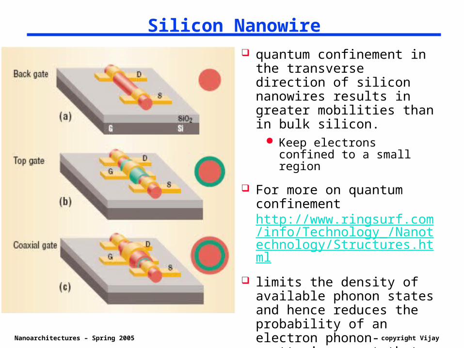
Silicon Nanowire quantum confinement in
the transverse direction of silicon nanowires results in greater mobilities than in bulk silicon.
Keep electrons confined to a small region
For more on quantum confinement http://www.ringsurf.com/info/Technology_/Nanotechnology/Structures.html
limits the density of available phonon states and hence reduces the probability of an electron phonon-scattering event—that is, it reduces drag.
Nanoarchitectures – Spring 2005 copyright Vijay
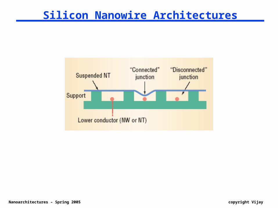
Why Silicon Nanowires? The performance of these isolated devices cannot
in general compete with scaled silicon on speed.
Their potential lies in achieving increased density and reducing fabrication costs.
Proponents of cross-bar architectures argue that arrays of these devices can be “self-assembled” using fluidic assembly and Langmuir-Blodgett techniques.
The major problems are in providing the gain necessary for signal restoration and fan out and to connect the self-assembled modules to global control lines.
Nanoarchitectures – Spring 2005 copyright Vijay
Silicon Nanowire Architectures
Nanoarchitectures – Spring 2005 copyright Vijay
Architectures
Nanoarchitectures – Spring 2005 copyright Vijay
Quantum Cellular Architecture QCA straddles the line between being a new
architecture and a new device, clearly demonstrating that new architectures may be required to support new devices.
In the QCA paradigm, a locally interconnected architecture consists of a regular array of cells containing several quantum dots.
Electrostatic interactions, not wires, provide the coupling between the cells. When we inject an electron pair into the cell, this electron pair’s orientation defines the cell’s state.
Electrical or Magnetic
Nanoarchitectures – Spring 2005 copyright Vijay
QCAs - Cons Grid style QCA architectures would be
extraordinarily inefficient in terms of area.
However, by departing from the regular grid structure, it is possible to design EQCA structures that could carry out universal computing with moderate efficiency.
However, current device and circuit analyses indicate that the speed of EQCA circuits will be limited to less than about 10 MHz.
Nanoarchitectures – Spring 2005 copyright Vijay
Defect Tolerant Architectures The general idea behind defect-tolerant
architectures is conceptually the opposite of traditional architectures
Designers fabricate a generic set of wires and switches, then they configure the resources by setting switches that link them together to obtain the desired functionality.
A cornerstone of defect-tolerant systems is redundancy of hardware resources—switches, memory cells, and wires—which implies very high integration density.
Fabrication could potentially be very inexpensive if researchers can actualize a chemical self-assembly and attach global interconnects
Nanoarchitectures – Spring 2005 copyright Vijay
Fault vs defect tolerance It is important to differentiate between defect-
tolerant and fault-tolerant architectures.
Fault-tolerant systems are designed to deal with transient faults and usually require some form of redundancy checking.
Both defect-tolerant and fault-tolerant systems have an upper limit to the number of defects or faults they can handle before the correction process dominates the overall calculation efficency.
The numerical limit appears to be 20 to 25 percent bad elements or defective calculations.
Nanoarchitectures – Spring 2005 copyright Vijay
Phase Logic Phase logic is is closely associated with the use of
phase as a state variable.
Richard Feynman received a patent for what he called the Parameteron in the 1950s.
it is possible to store information as the relative phase of two oscillating analog signals in a tank oscillator circuit. One signal is labeled as the reference signal, and the other is labeled as the control signal.
Changing the phase of the control signal relative to the reference signal “changes state” and logic.
If the circuit has only two allowed relative phases, it is possible to implement both binary and multivalued logic.
More recent variation is tunneling phase logic
Nanoarchitectures – Spring 2005 copyright Vijay
Quantum Computing The core idea of quantum information processing
or quantum computing is that each individual component of an infinite superposition of
wave functions is manipulated in parallel achieving a massive speedup relative to conventional
computers. The challenge is to manipulate the wave functions so
that they perform a useful function and then to find a way to read the result of the calculation.
Implementations bulk resonance quantum implementations including
NMR, linear optics, and cavity quantum electrodynamics;
atomic quantum implementations including trapped ions and optical lattices;
solid-state quantum implementations including semiconductors and superconductors.
Nanoarchitectures – Spring 2005 copyright Vijay
State Variables The search for alternative logic devices must
embrace the concept of using state variables other than electric charge.
molecular state
spin orientation
electric dipole orientation
photon intensity or polarization
quantum state
phase state
mechanical state
Nanoarchitectures – Spring 2005 copyright Vijay
Economic Impact Risk of adjusted return on investment of any new
technology must exceed that of silicon is trivially true,
Herb Kroemer, recipient of the 2000 Nobel Prize in physics, cautions, sufficiently advanced technologies will create their own applications.
To estimate the total ROI for an emerging technology, in addition to markets that exist today, we also must anticipate future markets—and that’s tough.
Nanoarchitectures – Spring 2005 copyright Vijay
Technology Trends the bulk band structure of solids needs to be
replaced by geometry-dependent energetic structures of nanostructures, requiring us toanalyze their stability and their basic quantum mechanical energy levels;
doping, a bulk process, needs to be replaced by the precise manipulation and placement of individual atoms; and
crystal growth, another bulk process, needs to be replaced by the self-organization of matter and self-assembly of complex structures.
Nanoarchitectures – Spring 2005 copyright Vijay
Next Lecture Lithography vs. Self Assembly
Reading List A PROMISING LITHOGRAPHY GETS STUCK, 56-57,
Spectrum January, 2004 A little light Magic, 34- , Spectrum, September 2003 Chip Makings Wet New technology, pp. 30- , Spectrum,
May 2004 New Frontiers: Self-Assembly and Nanoelectronics,
Computer, January 2001, pp 34-
Nanoarchitectures – Spring 2005 copyright Vijay
CSE 598 Nanoarchitectures
Spring 2005
Lecture 4: Lithography vs.
Self AssemblyVijay Narayanan (www.cse.psu.edu/~vijay)