note creating low power applications - nxp...
TRANSCRIPT

1 IntroductionThe MPC56xx family is a series of 32-bit microcontrollersbased on the Power Architecture® BookE and designedspecifically for embedded automotive applications.
This family contains a variety of low-power featuresincluding:
• Dynamic power management of core and peripherals• Software-controlled clock gating of peripherals• Multiple power domains to minimize leakage in low-
power modes
This document discusses the low-power features in detail andhow to use them effectively in an application to minimize theoverall power used by the device. Some information out of theMPC5607BRM : MPC5607B Microcontroller–ReferenceManual and AN2865: Qorivva Simple Cookbook, available onhttp://www.freescale.com is repeated for completeness andease of navigation. The MPC560xB microcontroller is used inexamples but in general, the features apply to other deviceswith the Mode Entry module.
NOTESome MCUs implementing the Mode Entrymodules do not have all low-power modesincorporated.
Freescale Semiconductor Document Number:AN4240
Application Note Rev. 0, 8/2012
Creating Low Power ApplicationsUsing the Mode Entry ModuleConfiguring Qorriva Microcontrollers to MinimizePower Consumption
by: Chris Platt, Armin Winter, Carl Culshaw, and Steve MihalikAutomotive and Industrial Solutions Group
© 2012 Freescale Semiconductor, Inc.
General Business Information
Contents
1 Introduction............................................................1
2 The power problem.................................................2
3 Low-Power feature summary..................................2
4 Clock description....................................................3
5 Power control unit...................................................4
6 Mode Entry (ME) module.......................................6
7 Pins during low-power modes..............................21
8 Low-Power mode entry........................................22
9 Low-power wake-up features...............................27
10 Low-power mode exit............................................39
11 Current consumption.............................................48
12 Common mistakes.................................................49
13 Appendix: Debugging with low-powermode......................................................................49
2 The power problemThere are two compnents that make up the total current consumed by a microcontroller, namely dynamic and static.
2.1 Dynamic currentThis is the main current prevalent during normal operating conditions. The mechanism responsible for this current isbasically due to charging and discharging the gates of the millions of MOS transistors that switch on and off as the deviceoperates. The switching currents adhere to the equation:
Thus, as technology advances and transistors become smaller, the gates become smaller resulting in lower gate capacitance.The lower capacitance means lower switching currents and hence an overall reduced dynamic run current.
The other side of the equation implies that increasing switching speeds (dv/dt) lead to an increased dynamic current.
The reduced current due to lower capacitance wins out over the increased current due to faster switching leading to a loweroverall dynamic power. Unfortunately, as applications become more complex and demanding, the performance requirementsand hence frequencies are increasing, leading to an overall increase in dynamic power.
2.2 Static currentThis current is present when the transistors of the device are not switching and are hence in a static state. The mainmechanism causing this current is leakage due to the finite resistance that exists between power and ground if power isapplied to a CMOS circuit.
This leakage current is highly dependent on the threshold voltage of the transistor. As advances in technology lead to eversmaller device sizes, supply voltage levels are scaled lower. To improve circuit speed, the threshold voltages are alsodecreased, resulting in an exponential increase in sub-threshold leakage current. In summary, as technology shrinks thedevice size, even though dynamic power trends lower, the required increase in performance means that any savings made bytechnology are neutralized by the increased frequencies. So, overall power is trending upward.
Couple this fact with a large increase in static leakage inherent due to smaller device sizes. So, the overall dynamic powerincreases with the static current becoming a larger component of the overall current.
3 Low-Power feature summaryBecause the low-power requirements are showing an upward trend, the MPC56xxB/C/D and several other Qorivva familymembers have a number of features that are specifically designed to minimize power consumption. This is achieved byinfluencing both the dynamic as well as the static constituent parts of power consumption.
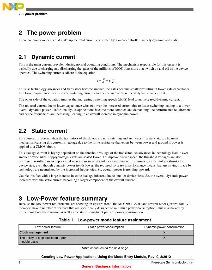
Table 1. Low-power mode feature assignment
Low-power feature Static power consumption Dynamic power consumption
Clock management X
The ability to stop clocks on a permodule basis
X
Table continues on the next page...
The power problem
Creating Low Power Applications Using the Mode Entry Module, Rev. 0, 8/2012
2 Freescale Semiconductor, Inc.General Business Information

Table 1. Low-power mode feature assignment (continued)
Optimized clock tree design X
Ability to divide down the system clock toperipherals
X
Ability to gate off or divide down theclock to the core
X
Onboard clocking X
Part can self-clock without a FMPLL X
16 MHz internal oscillator X
128 kHz internal oscillator X
Power gating X
Removing power to large areas of silicon X
Active well biasing (in Stop mode) X
Dual core (available on somederivatives)
X
Able to run at lower speed to achieve thesame throughput
X
4 Clock description
Clock description
Creating Low Power Applications Using the Mode Entry Module, Rev. 0, 8/2012
Freescale Semiconductor, Inc. 3General Business Information

Power consumption is directly linked to clock signal switching, that is, the power consumption increases if more gates areswitching. Within the MPC56xxB family, several methods are employed to avoid “wasting” power in clock edges:
• Clock freeze• CPU activity can be temporarily halted, for example, while waiting for an analog-to-digital conversion (ADC) to
complete. This is implemented using WAIT instruction, or STOP and HALT modes.• Peripheral bus division
• Using dividers in the Clock Generation module, can reduce clock rates, for example, in ADC and communicationports. All the modules don’t need to run at full system speed; the clocks can be slowed down in each module tosave power.
• Clock Gating• Applied wherever possible and at the entry to each sub-module (peripheral). Switch off the clocks to any unused
module to save power. This is implemented using peripheral configurations in the Mode Entry module.
The MPC56xxB clock structure allows system clock selection and dividing clocks to most of the peripherals.
Table 2. Clock source behaviorsummary
Clock source Start-up time Power consumption Check errors
FIRC:
16 MHz internal RC oscillator
.
Low (< 1 µs) Medium (< 50 µA) Low (> 10%)
SIRC:
128 kHz internal RC oscillator
Low (< 1 µs) Low (<1 µA) Low (> 10%)
SXOSC:
32 kHz external crystal oscillator
.
High (ms) Low (<10 µA) High (< 1%)
FXOSC:
4–16 MHz external crystal oscillator
.
High (ms) High (>100 µA) High (< 1%)
FMPLL High (ms) High (>1 mA) High (< 1%)
5 Power control unitThe purpose of the power control unit (PCU) is to reduce overall device power consumption. The MCU peripherals areallocated to various power domains. The PCU allows users to remove or apply power to a power domain (PD) depending onthe operating mode.
Hardware is used to control switching power on and off to primary power domains (PD0 and PD1) based on the mode beingentered to conserve current. When a domain is powered off, then all initialization and other data is lost for registers andmemory in that domain. Unlike power domains PD0 and PD1, power for PD2 is configurable by software writing to thePCU_PCONF2 register.
Power control unit
Creating Low Power Applications Using the Mode Entry Module, Rev. 0, 8/2012
4 Freescale Semiconductor, Inc.General Business Information

Going to STANDBY mode cuts power to the core, most of the peripherals, mode entry configurations, clocks, and so on.Therefore, registers in PD0 and PD1 need to be reinitialized when exiting the STANDBY mode, but not for other modes suchas STOP mode.
5.1 Power domain control• Power domains are controlled on a device mode basis.• For each mode, software can configure whether certain power domains are connected to the supply voltage during the
power-up state, or disconnected during the power-down state.• Maximum power saving is reached by entering the STANDBY mode.• On each mode change request, the MC_PCU evaluates the power domain settings in the power domain configuration
registers and initiates a power-down or a power-up sequence for each individual power domain.• The power-up/down sequences are handled by finite state machines to ensure a smooth and safe transition from one
power state to the other.• Exit from STANDBY mode can be made only via a system wake-up event as all power domains other than PD0 are in
the power-down state.
Figure 1. MPC5604/3/2B/C PCU block diagram
Table 3. MPC5604/3/2B/C PCU setup
Power Domain Contains State
PD0 Minimal circuitry for low power, includingfirst 8 KB SRAM, WKPU Unit, CANSampler, RTC, API, etc.
Always ON
Table continues on the next page...
Power control unit
Creating Low Power Applications Using the Mode Entry Module, Rev. 0, 8/2012
Freescale Semiconductor, Inc. 5General Business Information

Table 3. MPC5604/3/2B/C PCU setup (continued)
Power Domain Contains State
PD1 The rest of the device except SRAM STANDBY: OFF
Other Modes: ON
PD2 SRAM other than the first 8 KB SRAM Configurable for each mode
All memories which are not powered down during STANDBY mode automatically enter a power saving state. No softwareconfiguration is required to enable this power-saving state.
NOTEPCU setup of other derivatives might contain an additional power domain with a slightlydifferent configuration. See the reference manual of the corresponding device of theMPC56xx family, available on http://www.freescale.com.
6 Mode Entry (ME) module
6.1 OverviewThe Mode Entry (ME) module controls the device mode and mode transition sequences in all functional states. It alsocontains configuration, control and status registers accessible for the application. By supporting a variety of modes, itaccommodates different application needs. Each mode is configurable and can be setup to achieve an optimum betweenpower management and system performance requirements.
Modes can be preconfigured during device initialization and mode changes are triggered by a simple software (SW)sequence. Therefore, it offers a centralized and easy way to switch between modes depending on application needs.
An additional low-power mode configuration example is given within application note AN2865: Qorivva Simple Cookbook,which is available for download from http://www.freescale.com.
Mode Entry (ME) module
Creating Low Power Applications Using the Mode Entry Module, Rev. 0, 8/2012
6 Freescale Semiconductor, Inc.General Business Information
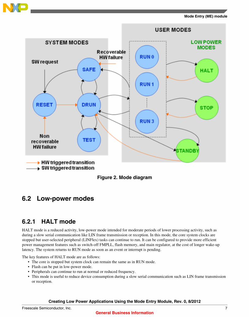
Figure 2. Mode diagram
6.2 Low-power modes
6.2.1 HALT modeHALT mode is a reduced activity, low-power mode intended for moderate periods of lower processing activity, such asduring a slow serial communication like LIN frame transmission or reception. In this mode, the core system clocks arestopped but user-selected peripheral (LINFlex) tasks can continue to run. It can be configured to provide more efficientpower management features such as switch-off FMPLL, flash memory, and main regulator, at the cost of longer wake-uplatency. The system returns to RUN mode as soon as an event or interrupt is pending.
The key features of HALT mode are as follows:• The core is stopped but system clock can remain the same as in RUN mode.• Flash can be put in low-power mode.• Peripherals can continue to run at normal or reduced frequency.• This mode is useful to reduce device consumption during a slow serial communication such as LIN frame transmission
or reception.
Mode Entry (ME) module
Creating Low Power Applications Using the Mode Entry Module, Rev. 0, 8/2012
Freescale Semiconductor, Inc. 7General Business Information

• Analog device components such as phase-locked loop (PLL), analog-to-digital converter (ADC), and potentially themain voltage regulator, can be stopped.
• PLL can be configured to be on or off (default is off).
6.2.2 WAIT instructionThe MPC56xx e200 CPUs support a WAIT instruction. Executing this WAIT instruction has a similar effect as enteringHALT mode. By executing the WAIT instruction, only the CPU clock gets stopped, whereas in HALT mode, the coreplatform clock gets stopped which causes additional functionality like System Timer Module (STM), Crossbar Switch(XBAR), and other modules, to be halted. As a consequence, current consumption after executing the WAIT instruction ishigher compared to HALT mode.
This is the only low-power mode not configured and entered by the ME module. With only four system clock cycles, a veryshort wake-up latency is supported.
6.2.3 STOP modeSTOP mode maintains power to the entire device allowing the retention of all on-chip registers and memory, and providing afaster recovery low-power mode than STANDBY mode which offers the lowest power consumption. There is no need toreconfigure the device before executing code. The clocks to the core and peripherals are halted and can be optionally stoppedat the expense of a slower startup time. FMPLL is always disabled during STOP mode. During STOP mode exit, the FIRC isused to clock the part until the target clock is available.
STOP is entered from RUN mode only. Wake-up from STOP mode is triggered by an external event or by the internalperiodic wake-up, if enabled.
The key features of STOP mode are as follows:• The core provides additional low-power features beyond HALT.• Active clock gating is used to segment the device.• External oscillator is stopped, but can be allowed to run to support fast startup at the expense of added power.• The entire device is powered and RAM is retained.• RTC and API can continue to run.• PLL is always off.• It has the option to support fast and slow IRC.• System clock can be disabled.• PLL is always disabled.• System clock is only FIRC upon immediate STOP mode exit until the target clock is ready.
6.2.4 STANDBY modeSTANDBY mode halts the clock to the entire device and turns off the power to the majority of the chip to offer the lowestpossible power consumption.
The device can be woken up from STANDBY mode by any of the external wake-up pins, a reset, or from a periodic wake-upusing a low-power oscillator. If required, it is possible to enable the internal 16 MHz or 128 kHz RC oscillator or external 32kHz oscillator (not available on all derivatives). In STANDBY mode, the contents of the cores, on-chip peripheral registersand potentially some of the volatile memory are not held.
Depending on the user configuration, either 32 KB, or 8 KB of SRAM are retained (MPC5604B). A fast wake-up using theon-chip 16 MHz internal RC oscillator allows rapid execution from RAM on exit from low-power modes. This oscillatorsupports low-speed code execution and clocking of peripherals through selection as the system clock, and it can be used asthe FMPLL input clock source to provide fast startup without the external oscillator delay.
Mode Entry (ME) module
Creating Low Power Applications Using the Mode Entry Module, Rev. 0, 8/2012
8 Freescale Semiconductor, Inc.General Business Information

In low-power modes, the internal 16 MHz RC oscillator also supports the operation of ADCs. External wake-up pins areavailable for wake-up, and a fast startup internal voltage regulator provides a rapid exit from low-power modes.
The key features of STANDBY mode are:• This mode consumes the lowest possible power.• Most functions (digital and analog) of the device are not powered.• Remains only the back-up logic. For example, RTC/API, preserves wake-up inputs, part of SRAM.• On STANDBY exit, the processor uses the RESET vector or a SRAM Vector, if enabled.• Wake-up from selected I/O or API/RTC• WISR register in the WKPU can be used to verify the wake-up source.• Data saved prior to mode entry can be recovered on exit from the mode, if needed.• Selectable size of RAM supported: 8 KB or all RAM• Optionally enabled low-speed IRC
6.3 Low-Power Peripheral Configuration registersEach peripheral can be associated with a particular clock gating policy. The policy is determined by two groups of peripheralconfiguration registers:
• ME_RUN_PC0:7 for RUN modes• ME_LP_PC0:7 for low-power modes
Clocks to peripherals are gated off unless enabled for that mode.
Figure 3. Low-Power Peripheral Configuration registers (ME_LP_PC0…7)
Along these registers, a selection of eight low-power mode configurations for peripherals can be defined. There is anequivalent register set (ME_RUN_PC0…7) for run modes available.
Table 4. Low-Power Peripheral Configuration registers (ME_LP_PC0…7) field descriptions
Field Description
STANDBY Peripheral control during STANDBY
0 Peripheral is frozen with clock gated.1 Peripheral is active.
Table continues on the next page...
Mode Entry (ME) module
Creating Low Power Applications Using the Mode Entry Module, Rev. 0, 8/2012
Freescale Semiconductor, Inc. 9General Business Information
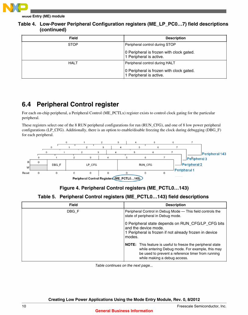
Table 4. Low-Power Peripheral Configuration registers (ME_LP_PC0…7) field descriptions(continued)
Field Description
STOP Peripheral control during STOP
0 Peripheral is frozen with clock gated.1 Peripheral is active.
HALT Peripheral control during HALT
0 Peripheral is frozen with clock gated.1 Peripheral is active.
6.4 Peripheral Control registerFor each on-chip peripheral, a Peripheral Control (ME_PCTLx) register exists to control clock gating for the particularperipheral.
These registers select one of the 8 RUN peripheral configurations for run (RUN_CFG), and one of 8 low power peripheralconfigurations (LP_CFG). Additionally, there is an option to enable/disable freezing the clock during debugging (DBG_F)for each peripheral.
Figure 4. Peripheral Control registers (ME_PCTL0…143)
Table 5. Peripheral Control registers (ME_PCTL0…143) field descriptions
Field Description
DBG_F Peripheral Control in Debug Mode — This field controls thestate of peripheral in Debug mode.
0 Peripheral state depends on RUN_CFG/LP_CFG bits and the device mode.1 Peripheral is frozen if not already frozen in device modes.
NOTE: This feature is useful to freeze the peripheral statewhile entering Debug mode. For example, this maybe used to prevent a reference timer from runningwhile making a debug access.
Table continues on the next page...
Mode Entry (ME) module
Creating Low Power Applications Using the Mode Entry Module, Rev. 0, 8/2012
10 Freescale Semiconductor, Inc.General Business Information

Table 5. Peripheral Control registers (ME_PCTL0…143) field descriptions (continued)
Field Description
LP_CFG Peripheral Configuration Select for Non-RUN modes—Thisfield associates a configuration as defined in theME_LP_PC0…7 registers to the peripheral.
000 Selects ME_LP_PC0 configuration001 Selects ME_LP_PC1 configuration010 Selects ME_LP_PC2 configuration011 Selects ME_LP_PC3 configuration100 Selects ME_LP_PC4 configuration101 Selects ME_LP_PC5 configuration110 Selects ME_LP_PC6 configuration111 Selects ME_LP_PC7 configuration
RUN_CFG Peripheral Configuration Select for RUN modes—This fieldassociates a configuration as defined in the ME_RUN_PC0…7 registers to the peripheral.
000 Selects ME_RUN_PC0 configuration001 Selects ME_RUN_PC1 configuration010 Selects ME_RUN_PC2 configuration011 Selects ME_RUN_PC3 configuration100 Selects ME_RUN_PC4 configuration101 Selects ME_RUN_PC5 configuration110 Selects ME_RUN_PC6 configuration111 Selects ME_RUN_PC7 configuration
6.5 Peripheral Status registerThis set of read-only registers provides the status of the peripherals.
Mode Entry (ME) module
Creating Low Power Applications Using the Mode Entry Module, Rev. 0, 8/2012
Freescale Semiconductor, Inc. 11General Business Information
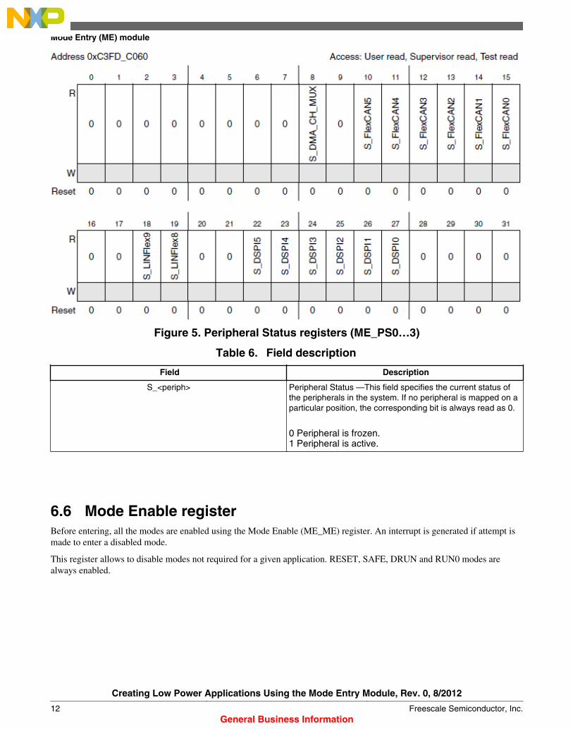
Figure 5. Peripheral Status registers (ME_PS0…3)
Table 6. Field description
Field Description
S_<periph> Peripheral Status —This field specifies the current status ofthe peripherals in the system. If no peripheral is mapped on aparticular position, the corresponding bit is always read as 0.
0 Peripheral is frozen.1 Peripheral is active.
6.6 Mode Enable registerBefore entering, all the modes are enabled using the Mode Enable (ME_ME) register. An interrupt is generated if attempt ismade to enter a disabled mode.
This register allows to disable modes not required for a given application. RESET, SAFE, DRUN and RUN0 modes arealways enabled.
Mode Entry (ME) module
Creating Low Power Applications Using the Mode Entry Module, Rev. 0, 8/2012
12 Freescale Semiconductor, Inc.General Business Information

Figure 6. Mode Enable (ME_ME) register
Table 7. Mode Enable (ME_ME) register field descriptions
Field Description
STANDBY STANDBY mode enable
0 STANDBY mode is disabled.1 STANDBY mode is enabled.
STOP STOP mode enable
0 STOP mode is disabled.1 STOP mode is enabled.
HALT HALT mode enable
0 HALT mode is disabled.1 HALT mode is enabled.
RUN3 RUN3 mode enable
0 RUN3 mode is disabled.1 RUN3 mode is enabled.
RUN2 RUN2 mode enable
0 RUN2 mode is disabled.1 RUN2 mode is enabled.
RUN1 RUN1 mode enable
0 RUN1 mode is disabled.1 RUN1 mode is enabled.
Table continues on the next page...
Mode Entry (ME) module
Creating Low Power Applications Using the Mode Entry Module, Rev. 0, 8/2012
Freescale Semiconductor, Inc. 13General Business Information
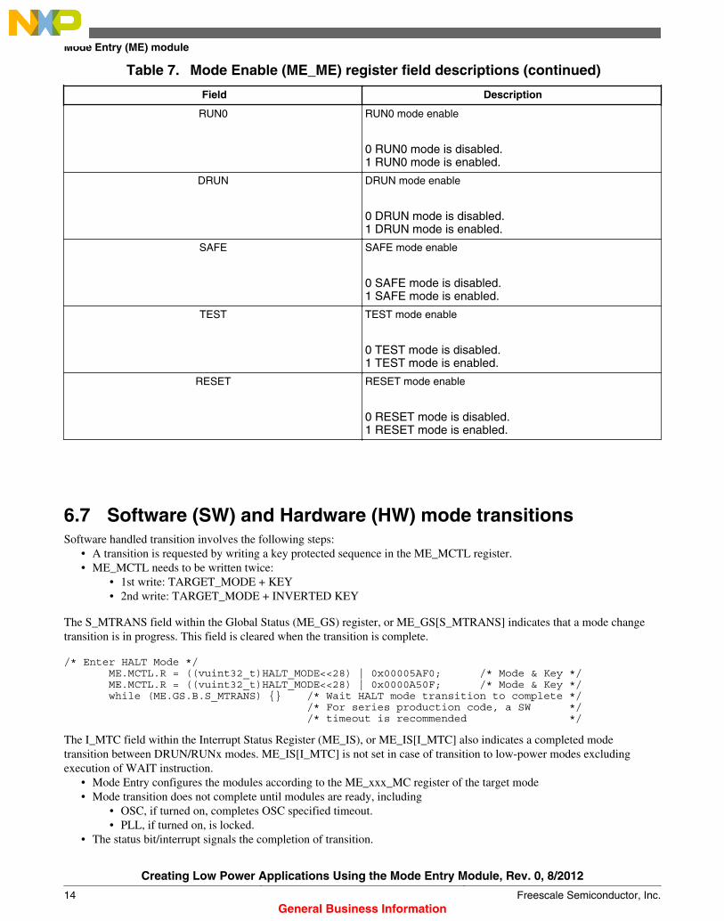
Table 7. Mode Enable (ME_ME) register field descriptions (continued)
Field Description
RUN0 RUN0 mode enable
0 RUN0 mode is disabled.1 RUN0 mode is enabled.
DRUN DRUN mode enable
0 DRUN mode is disabled.1 DRUN mode is enabled.
SAFE SAFE mode enable
0 SAFE mode is disabled.1 SAFE mode is enabled.
TEST TEST mode enable
0 TEST mode is disabled.1 TEST mode is enabled.
RESET RESET mode enable
0 RESET mode is disabled.1 RESET mode is enabled.
6.7 Software (SW) and Hardware (HW) mode transitionsSoftware handled transition involves the following steps:
• A transition is requested by writing a key protected sequence in the ME_MCTL register.• ME_MCTL needs to be written twice:
• 1st write: TARGET_MODE + KEY• 2nd write: TARGET_MODE + INVERTED KEY
The S_MTRANS field within the Global Status (ME_GS) register, or ME_GS[S_MTRANS] indicates that a mode changetransition is in progress. This field is cleared when the transition is complete.
/* Enter HALT Mode */ ME.MCTL.R = ((vuint32_t)HALT_MODE<<28) | 0x00005AF0; /* Mode & Key */ ME.MCTL.R = ((vuint32_t)HALT_MODE<<28) | 0x0000A50F; /* Mode & Key */ while (ME.GS.B.S_MTRANS) /* Wait HALT mode transition to complete */ /* For series production code, a SW */ /* timeout is recommended */
The I_MTC field within the Interrupt Status Register (ME_IS), or ME_IS[I_MTC] also indicates a completed modetransition between DRUN/RUNx modes. ME_IS[I_MTC] is not set in case of transition to low-power modes excludingexecution of WAIT instruction.
• Mode Entry configures the modules according to the ME_xxx_MC register of the target mode• Mode transition does not complete until modules are ready, including
• OSC, if turned on, completes OSC specified timeout.• PLL, if turned on, is locked.
• The status bit/interrupt signals the completion of transition.
Mode Entry (ME) module
Creating Low Power Applications Using the Mode Entry Module, Rev. 0, 8/2012
14 Freescale Semiconductor, Inc.General Business Information

NOTEModification of a ME_xxx_MC register (even the current one) is taken into account onnext mode “xxx” entry.
Hardware triggered transition involves:• Exit from low-power mode• SAFE transition caused by HW failure• RESET transition caused by HW failure
6.8 Mode Global Status registerThis register contains the global mode status.
It is recommended that software poll ME_GS[S_MTRANS] after requesting a transition to HALT, STOP, or STANDBY.
Figure 7. Global Status (ME_GS) register
Mode Entry (ME) module
Creating Low Power Applications Using the Mode Entry Module, Rev. 0, 8/2012
Freescale Semiconductor, Inc. 15General Business Information
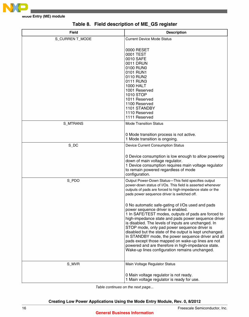
Table 8. Field description of ME_GS register
Field Description
S_CURREN T_MODE Current Device Mode Status
0000 RESET0001 TEST0010 SAFE0011 DRUN0100 RUN00101 RUN10110 RUN20111 RUN31000 HALT1001 Reserved1010 STOP1011 Reserved1100 Reserved1101 STANDBY1110 Reserved1111 Reserved
S_MTRANS Mode Transition Status
0 Mode transition process is not active.1 Mode transition is ongoing.
S_DC Device Current Consumption Status
0 Device consumption is low enough to allow powering down of main voltage regulator.1 Device consumption requires main voltage regulator to remain powered regardless of modeconfiguration.
S_PDO Output Power-Down Status—This field specifies outputpower-down status of I/Os. This field is asserted wheneveroutputs of pads are forced to high-impedance state or thepads power sequence driver is switched off.
0 No automatic safe-gating of I/Os used and pads power sequence driver is enabled.1 In SAFE/TEST modes, outputs of pads are forced to high-impedance state and pads power sequence driver is disabled. The levels of inputs are unchanged. In STOP mode, only pad power sequence driver is disabled but the state of the output is kept unchanged. In STANDBY mode, the power sequence driver and all pads except those mapped on wake-up lines are not powered and are therefore in high-impedance state. Wake-up lines configuration remains unchanged.
S_MVR Main Voltage Regulator Status
0 Main voltage regulator is not ready.1 Main voltage regulator is ready for use.
Table continues on the next page...
Mode Entry (ME) module
Creating Low Power Applications Using the Mode Entry Module, Rev. 0, 8/2012
16 Freescale Semiconductor, Inc.General Business Information
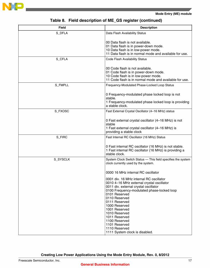
Table 8. Field description of ME_GS register (continued)
Field Description
S_DFLA Data Flash Availability Status
00 Data flash is not available.01 Data flash is in power-down mode.10 Data flash is in low-power mode.11 Data flash is in normal mode and available for use.
S_CFLA Code Flash Availability Status
00 Code flash is not available.01 Code flash is in power-down mode.10 Code flash is in low-power mode.11 Code flash is in normal mode and available for use.
S_FMPLL Frequency-Modulated Phase-Locked Loop Status
0 Frequency-modulated phase locked loop is not stable.1 Frequency-modulated phase locked loop is providing a stable clock.
S_FXOSC Fast External Crystal Oscillator (4–16 MHz) status
0 Fast external crystal oscillator (4–16 MHz) is not stable1 Fast external crystal oscillator (4–16 MHz) is providing a stable clock
S_FIRC Fast Internal RC Oscillator (16 MHz) Status
0 Fast internal RC oscillator (16 MHz) is not stable.1 Fast internal RC oscillator (16 MHz) is providing a stable clock.
S_SYSCLK System Clock Switch Status — This field specifies the systemclock currently used by the system.
0000 16 MHz internal RC oscillator
0001 div. 16 MHz internal RC oscillator0010 4–16 MHz external crystal oscillator0011 div. external crystal oscillator0100 Frequency-modulated phase-locked loop0101 Reserved0110 Reserved0111 Reserved1000 Reserved1001 Reserved1010 Reserved1011 Reserved1100 Reserved1101 Reserved1110 Reserved1111 System clock is disabled.
Mode Entry (ME) module
Creating Low Power Applications Using the Mode Entry Module, Rev. 0, 8/2012
Freescale Semiconductor, Inc. 17General Business Information

6.9 Mode Control registerThis register is used to trigger software-controlled mode changes. In order to change modes, the target mode must be writtento the register with the KEY. The next command must be another write to the register with the same mode and theINVERTED KEY.
Figure 8. Mode Control (ME_MCTL) register
Mode Entry (ME) module
Creating Low Power Applications Using the Mode Entry Module, Rev. 0, 8/2012
18 Freescale Semiconductor, Inc.General Business Information

Table 9. Mode Control (ME_MCTL) register field descriptions
Field Description
TARGET_MODE Target Device Mode
This field provides the target device mode to be entered by software programming. The mechanism to enter into any mode by software requires the write operation twice: first time with key, and second time with inverted key. This field is automatically updated by hardware while entering SAFE on hardware request. Also, while exiting from the HALT and STOP modes on hardware exit events, this field is updated with the appropriate RUN0…3 mode value.
0000 RESET0001 TEST0010 SAFE0011 DRUN0100 RUN00101 RUN10110 RUN20111 RUN31000 HALT1001 Reserved1010 STOP1011 Reserved1100 Reserved1101 STANDBY1110 Reserved1111 Reserved
KEY Control Key
This field enables write access to this register. Any write access to the register with a value different from the keys is ignored. Read access will always return the inverted key.
KEY: 0101101011110000 (0x5AF0)INVERTED KEY: 1010010100001111 (0xA50F)
6.10 Mode Entry module summaryMode transition allows:
• Enabling/disabling system clock sources• Selecting appropriate system clock• Gating clocks to peripherals• Dividing peripheral clocks on a set basis, as per the requirement
Mode Entry (ME) module
Creating Low Power Applications Using the Mode Entry Module, Rev. 0, 8/2012
Freescale Semiconductor, Inc. 19General Business Information

Figure 9. ME resource control overview
Mode Entry (ME) module
Creating Low Power Applications Using the Mode Entry Module, Rev. 0, 8/2012
20 Freescale Semiconductor, Inc.General Business Information
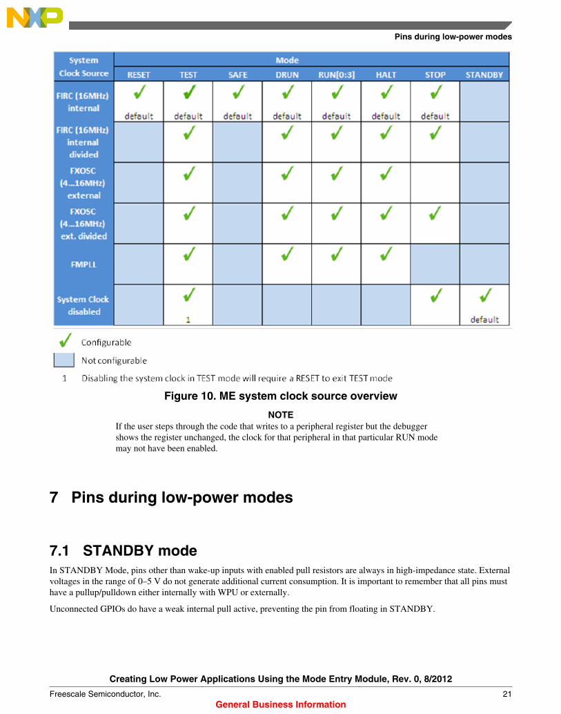
Figure 10. ME system clock source overview
NOTEIf the user steps through the code that writes to a peripheral register but the debuggershows the register unchanged, the clock for that peripheral in that particular RUN modemay not have been enabled.
7 Pins during low-power modes
7.1 STANDBY modeIn STANDBY Mode, pins other than wake-up inputs with enabled pull resistors are always in high-impedance state. Externalvoltages in the range of 0–5 V do not generate additional current consumption. It is important to remember that all pins musthave a pullup/pulldown either internally with WPU or externally.
Unconnected GPIOs do have a weak internal pull active, preventing the pin from floating in STANDBY.
Pins during low-power modes
Creating Low Power Applications Using the Mode Entry Module, Rev. 0, 8/2012
Freescale Semiconductor, Inc. 21General Business Information

NOTEThe statements given above regarding STANDBY do not apply to wake-up pins. Forwake-up pins, the internal pull selection needs to be aligned to the external voltages toavoid additional current consumption.
In summary, all wake-up pads, including those not bonded out to pins, must be correctly configured to achieve low-powerusage in STANDBY mode. GPIOs without wake-up capability do not need special configuration for STANDBY mode.
Pins having both the wake-up and analog functionality such as PB[10], PD[0:1] on MPC5607/6/5B/C and MPC5602/1D, orPB[10] on MPC5604/3/2B/C, must be driven either high-level or low-level (possibly using the internal pullup) duringSTANDBY.
In case these pins are connected to external component providing analog signal, it is important to check this external analogsignal is either lower than 0.2*VDD_HV or higher than 0.8*VDD_HV not to incur extra consumption.
The TDO pad has been moved into the STANDBY domain (PD0) in order to allow low-power debug handshaking inSTANDBY mode. However, no pullup resistor is active on the TDO pad while in STANDBY mode. At this time the pad isconfigured as an input. When no debugger is connected, the TDO pad is floating causing additional current consumption.
To avoid the extra consumption, TDO must be connected. An external pullup resistor in the range of 47–100 kΩ must beadded between the TDO pin and VDD. If the TDO pin is used as application pin and a pullup cannot be used, then apulldown resistor with the same value must be used between TDO pin and GND instead.
On MPC5604/3/2/B/C, wake-up line functionality on PB[8], PB[9] is not available in STANDBY mode. These pads are notsupplied with ultra low-power regulator, but are driven from main regulator which is switched off in STANDBY mode.
7.2 STOP modeDuring STOP mode, status of pins will be kept unchanged. In this case, the internal pull selection needs to be aligned to theexternal voltages to avoid additional current consumption in STOP mode.
Leaving input pins floating will cause the pin voltage to float to any voltage depending upon leakages to ground and thesupply. Noise will cause the CMOS inverter or gate to which the input is connected to go into an indefinite and high-powerdissipation mode, with both N- and P-channel outputs conducting.
Based on this effect, external noise can cause the input stage to switch states at high-frequency (oscillations). Switching fromone state to the other will add additional current consumption to the static leakage current. Also, an increased level of noisegets injected to the microcontroller.
8 Low-Power mode entryLow-power mode entry is controlled by software requests only.
CAUTIONThe ME module will not allow low-power mode entry, if it detects a pending wake-upevent or pending interrupt request. While examining for a pending interrupt request, theME module ignores the MSR[EE] state and peripheral's interrupt priorities in theinterrupt controller (INTC). The ME module effectively looks at peripheral flags andtheir associated interrupt enable bit state.
Low-Power mode entry
Creating Low Power Applications Using the Mode Entry Module, Rev. 0, 8/2012
22 Freescale Semiconductor, Inc.General Business Information

The following table lists various RUN modes from which the low-power modes can be entered.
Table 10. Low-power mode entry
WAIT STOP HALT STANDBY
Software request fromDRUN
Yes No No Yes
Software request fromRUN0...3
Yes Yes Yes Yes
8.1 HALT mode entryHALT mode can be requested by SW from RUN0…3 modes.
For example:
void HALT_Mode_Entry(void) /* Enter HALT Mode */ ME.MCTL.R = 0x80005AF0; /* Mode & Key */ ME.MCTL.R = 0x8000A50F; /* Mode & Key */ while (ME.GS.B.S_MTRANS) /* Wait HALT mode transition to complete */
On MPC560xB/C/D derivatives, main VREG is not disabled during STOP or HALT mode:• If RUN[0..3] mode selects FXOSC to be running.• The target mode selects FXOSC as system clock.
If STOP or HALT is configured with:• ME_[mode]_MC.MVRON = 0• ME_[mode]_MC.FIRCON = 0, and• ME_[mode]_MC.SYSCLK = 0010/0011, the main VREG will nevertheless remain enabled during the STOP mode if
the previous RUN[0..3] mode is configured with ME_RUN[0..3]_MC.FXOSCON = 1. This will result in higher powerconsumption than expected.
Before entering STOP or HALT mode with the following configuration:• ME_[mode]_MC.MVRON = 0• ME_[mode]_MC.FIRCON = 0• ME_[mode]_MC.SYSCLK = 0010/0011, ensure the RUN[0..3] mode switches off FXOSC and
ME_RUN[0..3]_MC.FXOSCON = 0 before attempting to enter the low-power mode.
8.2 STOP mode entrySTOP mode can be requested by SW from RUN0…3 modes.
For example:
void STOP_Mode_Entry(void) /* Enter STOP Mode */ ME.MCTL.R = 0xA0005AF0; /* Mode & Key */ ME.MCTL.R = 0xA000A50F; /* Mode & Key */ while (ME.GS.B.S_MTRANS) /* Wait STOP mode transition to complete */
Low-Power mode entry
Creating Low Power Applications Using the Mode Entry Module, Rev. 0, 8/2012
Freescale Semiconductor, Inc. 23General Business Information
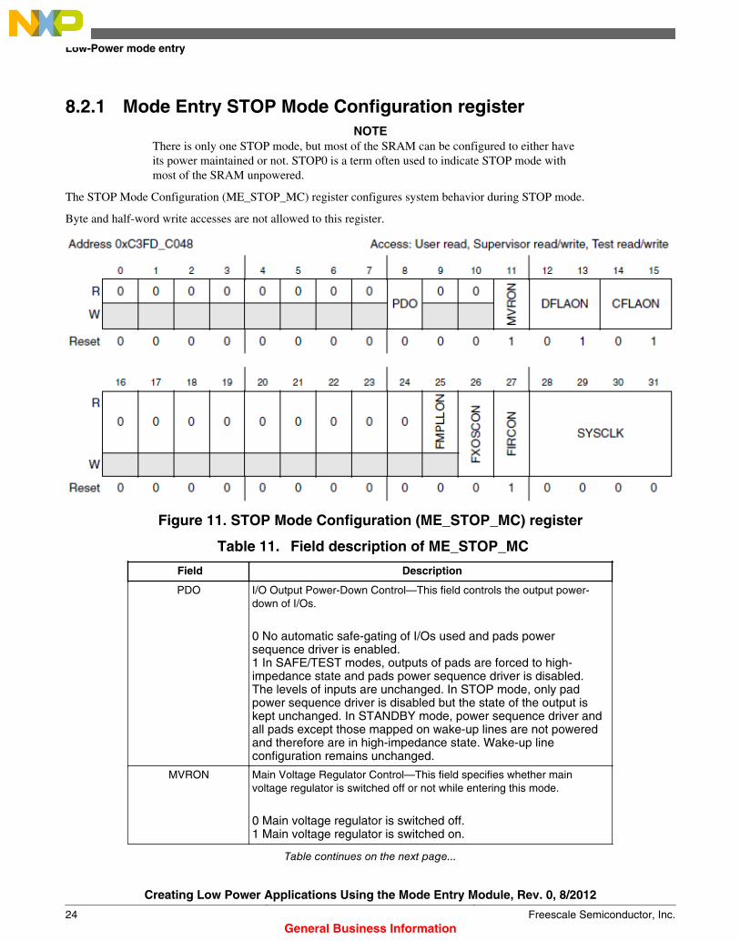
8.2.1 Mode Entry STOP Mode Configuration registerNOTE
There is only one STOP mode, but most of the SRAM can be configured to either haveits power maintained or not. STOP0 is a term often used to indicate STOP mode withmost of the SRAM unpowered.
The STOP Mode Configuration (ME_STOP_MC) register configures system behavior during STOP mode.
Byte and half-word write accesses are not allowed to this register.
Figure 11. STOP Mode Configuration (ME_STOP_MC) register
Table 11. Field description of ME_STOP_MC
Field Description
PDO I/O Output Power-Down Control—This field controls the output power-down of I/Os.
0 No automatic safe-gating of I/Os used and pads power sequence driver is enabled.1 In SAFE/TEST modes, outputs of pads are forced to high-impedance state and pads power sequence driver is disabled. The levels of inputs are unchanged. In STOP mode, only pad power sequence driver is disabled but the state of the output is kept unchanged. In STANDBY mode, power sequence driver and all pads except those mapped on wake-up lines are not powered and therefore are in high-impedance state. Wake-up line configuration remains unchanged.
MVRON Main Voltage Regulator Control—This field specifies whether mainvoltage regulator is switched off or not while entering this mode.
0 Main voltage regulator is switched off.1 Main voltage regulator is switched on.
Table continues on the next page...
Low-Power mode entry
Creating Low Power Applications Using the Mode Entry Module, Rev. 0, 8/2012
24 Freescale Semiconductor, Inc.General Business Information

Table 11. Field description of ME_STOP_MC (continued)
Field Description
DFLAON Data Flash Power-Down Control—This field specifies the operating modeof the data flash after entering this mode.
00 Reserved01 Data flash is in power-down mode.10 Data flash is in low-power mode.11 Data flash is in normal mode.
CFLAON Code Flash Power-Down Control—This field specifies the operating modeof the program flash after entering this mode.
00 Reserved01 Code flash is in power-down mode.10 Code flash is in low-power mode.11 Code flash is in normal mode.
FMPLLON Frequency-Modulated Phase Locked Loop Control
0 Frequency-modulated phase-locked loop is switched off.1 Frequency-modulated phase-locked loop is switched on.
FXOSCON Fast External Crystal Oscillator (4–16 MHz) control
0 Fast external crystal oscillator (4–16 MHz) is switched off.1 Fast external crystal oscillator (4–16 MHz) is switched on.
FIRCON Fast Internal RC Oscillator (16 MHz) Control
0 Fast internal RC oscillator (16 MHz) is switched off.1 Fast internal RC oscillator (16 MHz) is switched on.
SYSCLK System Clock Switch Control—This field specifies the system clock to be used by the system.
0000 16 MHz internal RC oscillator0001 div. 16 MHz internal RC oscillator0010 4–16 MHz external crystal oscillator0011 div. external crystal oscillator0100 Frequency-modulated phase-locked loop0101 Reserved0110 Reserved0111 Reserved1000 Reserved1001 Reserved1010 Reserved1011 Reserved1100 Reserved1101 Reserved1110 Reserved1111 System clock is disabled.
Lowest possible STOP power consumption is achieved by following sequence:
void STOP_Mode_Entry(void)ME_STOP_MC.B.PDO=1; /* Pad power sequence driver disabled, */
Low-Power mode entry
Creating Low Power Applications Using the Mode Entry Module, Rev. 0, 8/2012
Freescale Semiconductor, Inc. 25General Business Information

/* but state of the output is kept */ME_STOP_MC.B.MVRON=0; /* Main Voltage regulator is off */ ME_STOP_MC.B.DFLAON=1; /* Data flash is in power-down mode */ME_STOP_MC.B.CFLAON=1; /* Code flash is in power-down mode */ME_STOP_MC.B.FMPLLON=0; /* FMPLL off (default status during STOP) */ME_STOP_MC.B.FIRCON=0; /* Fast internal RC oscillator off */ME_STOP_MC.B.FXOSCON=0 /* Fast external crystal oscillator off */ME_STOP_MC.B.SYSCLK=0xF; /* System clock is disabled */ADC_0.MCR.B.PWDN = 1; /* Power donw analog part of ADC0 */ /* MPC5607B/C: saving ~ 2.8mA in STOP */ADC_1.MCR.B.PWDN = 1; /* Power down analog part of the ADC1 */ /* MPC5607B saving ~ 1.9mA in STOP */ /* Please note, not all MPC56xxB derivates */ /* support two ADC modules. Also the */ /* amount of current might vary as */ /* different derivates support a different */ /* amount of ADC channels. Status of MDIS, */ /* FREEZE, HALT bits of digital */ /* peripherals have no impact on STOP */ /* power consumption */ /* For all peripherals not needed during */ /* STOP a Low- Power Peripheral */ /* Configuration Register (ME_LP_PC0…7) */ /* with STOP = 0 should be assigned to */ /* the corresponding Peripheral Control */ /* Registers (ME_PCTLx). *//* Enter STOP Mode */ME.MCTL.R = ((vuint32_t)STOP_MODE<<28) | 0x00005AF0; /* Mode & Key */ME.MCTL.R = ((vuint32_t)STOP_MODE<<28) | 0x0000A50F; /* Mode & Key */ while (ME.GS.B.S_MTRANS)/* Wait STOP mode transition to complete */
On MPC560xB/C/D derivatives, main VREG is not disabled during STOP or HALT mode if RUN[0..3] mode selectsFXOSC to be running and target mode selects FXOSC as system clock. If STOP or HALT is configured with:
• ME_[mode]_MC.MVRON = 0• ME_[mode]_MC.FIRCON = 0• ME_[mode]_MC.SYSCLK = 0010/0011, the main VREG will nevertheless remain enabled during the STOP mode if
the previous RUN[0..3] mode is configured with ME_RUN[0..3]_MC.FXOSCON = 1. This will result in higher powerconsumption than expected.
Before entering STOP or HALT mode with the following configuration:• ME_[mode]_MC.MVRON = 0• ME_[mode]_MC.FIRCON = 0• ME_[mode]_MC.SYSCLK = 0010/0011, ensure the RUN[0..3] mode switches off FXOSC and
ME_RUN[0..3]_MC.FXOSCON = 0, before attempting to low-power mode transition.
8.3 STANDBY mode entrySTANDBY mode can be requested by SW from DRUN and RUN[0...3] modes.
The lowest power consumption in STANDBY can be achieved by the following sequence:
void STANDBY_Mode_Entry(void) /* Configure STANDBY0 Mode for lowest consumption (only WUP Unit ON) */ /* Please note, WKPU (Wakeup Unit) is always enabled */ /* To generate an interrupt event triggered by a wakeup line, it is */ /* necessary to enable WKPU */ CAN_0.MCR.B.FRZ = 1;/* Errata e9140PS: */ CAN_1.MCR.B.FRZ = 1;/* STANDBY can not be entered if the FlexCAN */ CAN_2.MCR.B.FRZ = 1;/* peripheral is active. If any FlexCAN module */ CAN_3.MCR.B.FRZ = 1; /* is enabled at the MC_ME (ME_RUN_PCx/ME_PCTLx) */ CAN_4.MCR.B.FRZ = 1; /* and enabled at the FlexCAN module, */
Low-Power mode entry
Creating Low Power Applications Using the Mode Entry Module, Rev. 0, 8/2012
26 Freescale Semiconductor, Inc.General Business Information
CAN_5.MCR.B.FRZ = 1; /* (MCR.B.MDIS=0) STANDBY0 mode will not be */ /* entered, and the device will remain in DRUN or */ /* RUNx mode. */ /* Workaround: The FlexCAN module must be frozen */ /* by setting FLEXCANx_MCR[FRZ]=1 in DRUN or */ /* RUNx mode before entering STANDBY mode. */ ME.STANDBY0.B.PDO=1;/* Pad power sequence driver disabled, but state */ /* of the output is kept */ ME.STANDBY0.B.MVRON=0;/* Main Voltage regulator is off */ ME.STANDBY0.B.DFLAON=1; /* Data flash is in power-down mode */ ME.STANDBY0.B.CFLAON=1;/* Code flash is in power-down mode */ ME.STANDBY0.B.OSCON=0;/* Fast external crystal oscillator (4-16 MHz) off */ ME.STANDBY0.B.PLLON=0;/* FMPLL is off (default status during STOP0) */ ME.STANDBY0.B.SYSCLK=0xF; /* System clock disabled BEFORE RC switching off */ ME.STANDBY0.B.RCON=0;/* Fast internal RC oscillator (16 MHz) off */ /* Enter STANDBY Mode */ ME.MCTL.R = ((vuint32_t)STANDBY_MODE<<28) | 0x00005AF0; /* Mode & Key */ ME.MCTL.R = ((vuint32_t)STANDBY_MODE<<28) | 0x0000A50F; /* Mode & Key */ while(1) /* Wait STANDBY mode transition to complete – use timeout */
NOTE• All peripherals need to be configured as off within the ME_PCTLx registers prior
to the STANDBY mode entry, otherwise, a reset gets generated on wake-up and thewake-up source is not visible within the WKPU_WISR register.
• Do not deactivate system clock prescaler in CGM_SC_DCx register prior toSTANDBY mode entry, otherwise, the system will not be able to exit STANDBY.
9 Low-power wake-up featuresThere are two mechanisms that can be used for wake up from low-power modes.
• Input pin transition or RTC/API enabled using the WKPU (STANDBY, STOP modes only)• Peripheral interrupts (HALT, STOP modes only)
The WKPU offers external wake-up/interrupt support through:• 3 system interrupt vectors for up to 18 interrupt sources for MPC5602/3/4B/C/D• 3 system interrupt vectors for up to 18 interrupt sources for MPC5602/3/4B/C/D• 4 system interrupt vectors for up to 24 interrupt sources for MPC5605/6/7B/C/D• Analog glitch filter per each wake-up line• Independent interrupt mask• Edge detection• Configurable system wake-up triggering from all interrupt sources• Configurable pullup
The WKPU offers non-maskable interrupt support through:• Edge detection• One NMI source with bypassable glitch filter• Independent interrupt destination: non-maskable interrupt, critical interrupt, or machine check request
On-chip wakeup support is provided through:• Two wake-up sources (RTC and API)• Wake-up status mapped to same register as external wake-up/interrupt status
Low-power wake-up features
Creating Low Power Applications Using the Mode Entry Module, Rev. 0, 8/2012
Freescale Semiconductor, Inc. 27General Business Information

Figure 12. Wake-up unit (WKPU)
NOTEThe WKPU remains powered during low-power modes.
Each WKPU pin:• Can issue only a wake-up, or an interrupt, or both• Can be sensitive on rising, falling or both edges• Has an analog glitch filter, which can be separately enabled• Has an internal pullup
9.1 Low-power interruptsThe following points must be noted when using interrupts as a wake-up mechanism from low-power modes.
• MSE[EE] status does not affect low-power wake-up interrupts.• The INTC values do not affect low-power wake-up.• Only a peripheral's Flag and Interrupt Enable bit are required to notify the ME module to exit STOP or HALT modes.• If using an interrupt to wake-up from STOP mode, a system clock must be configured in STOP mode. (SYSCLK
cannot be 1111)
Low-power wake-up features
Creating Low Power Applications Using the Mode Entry Module, Rev. 0, 8/2012
28 Freescale Semiconductor, Inc.General Business Information
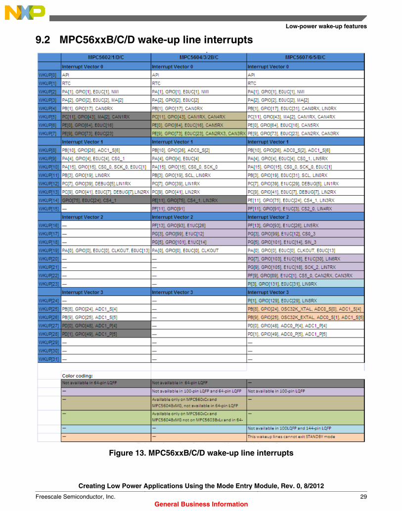
9.2 MPC56xxB/C/D wake-up line interrupts
Figure 13. MPC56xxB/C/D wake-up line interrupts
Low-power wake-up features
Creating Low Power Applications Using the Mode Entry Module, Rev. 0, 8/2012
Freescale Semiconductor, Inc. 29General Business Information
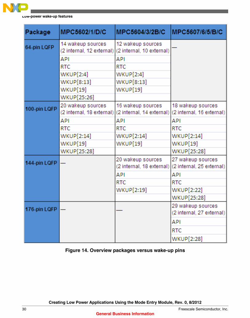
Figure 14. Overview packages versus wake-up pins
Low-power wake-up features
Creating Low Power Applications Using the Mode Entry Module, Rev. 0, 8/2012
30 Freescale Semiconductor, Inc.General Business Information

Figure 15. MPC5607B wake-up
NOTESmall packages do not contain all ports.
Low-power wake-up features
Creating Low Power Applications Using the Mode Entry Module, Rev. 0, 8/2012
Freescale Semiconductor, Inc. 31General Business Information
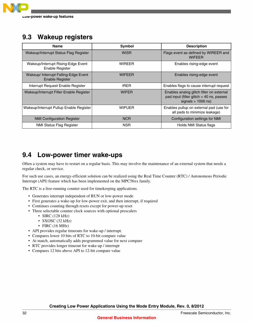
9.3 Wakeup registersName Symbol Description
Wakeup/Interrupt Status Flag Register WISR Flags event as defined by WIREER andWIFEER
Wakeup/Interrupt Rising-Edge EventEnable Register
WIREER Enables rising-edge event
Wakeup/ Interrupt Falling-Edge EventEnable Register
WIFEER Enables rising-edge event
Interrupt Request Enable Register IRER Enables flags to cause interrupt request
Wakeup/Interrupt Filter Enable Register WIFER Enables analog glitch filter on externalpad input (filter glitch < 40 ns, passes
signals > 1000 ns)
Wakeup/Interrupt Pullup Enable Register WIPUER Enables pullup on external pad (use forall pads to minimize leakage)
NMI Configuration Register NCR Configuration settings for NMI
NMI Status Flag Register NSR Holds NMI Status flags
9.4 Low-power timer wake-upsOften a system may have to restart on a regular basis. This may involve the maintenance of an external system that needs aregular check, or service.
For such use cases, an energy-efficient solution can be realized using the Real Time Counter (RTC) / Autonomous PeriodicInterrupt (API) feature which has been implemented on the MPC56xx family.
The RTC is a free-running counter used for timekeeping applications.
• Generates interrupt independent of RUN or low-power mode• First generates a wake-up for low-power exit, and then interrupt, if required• Continues counting through resets except for power-up reset• Three selectable counter clock sources with optional prescalers
• SIRC (128 kHz)• SXOSC (32 kHz)• FIRC (16 MHz)
• API provides regular timeouts for wake-up / interrupt.• Compares lower 10 bits of RTC to 10-bit compare value• At match, automatically adds programmed value for next compare• RTC provides longer timeout for wake-up / interrupt• Compares 12 bits above API to 12-bit compare value
Low-power wake-up features
Creating Low Power Applications Using the Mode Entry Module, Rev. 0, 8/2012
32 Freescale Semiconductor, Inc.General Business Information

Figure 16. RTC / API block diagram
NOTE32 kHz SXOSC option is not supported on all derivates.
As can be seen in Figure 16, the RTC clock source is selectable from the 16 MHz FIRC, 32 kHz SIRC, or 32 kHz SXOSC.RTC and API share a common 32-bit, free-running counter.
Table 13 , which has originally been published in the application note AN2865: Qorivva Simple Cookbook, shows RTC/APItimeouts based on different clock source and divider settings.
Low-power wake-up features
Creating Low Power Applications Using the Mode Entry Module, Rev. 0, 8/2012
Freescale Semiconductor, Inc. 33General Business Information

Table 13. RTC/API timeouts
Clocksource
div512
RTC_RTCC
[div512]
div 32RTC_RTCC [div 32]
RTCCounter
InputClock
Frequency
RTCCounter
InoutClock
Period (1⁄(RTC
CounterInputClockFreq.))
Min. APITimeout(1 x RTCCounter
inputclock
period)
Max. APITimeout
((210 - 1) xRTC
Counterinputclockperiod
Min. RTCTimeout
(210 xRTC
Counterinputclock
period)
Max. RTCTimeout
((222 - 1) xRTC
Counterinputclock
period)
RTCRolloverTimeout
(232 xRTC
Counterinputclock
period)
128 kHzSIRC1 withSIRCDIV=
0
0 0 128 kHz ~ 7.8 µs ~ 7.8 µs ~ 8 ms ~ 8 ms ~ 31 s ~ 8.9 h
0 1 4 kHz 250 µs 250 µs ~ 256 ms 256 ms ~ 17 min ~ 12 d
1 0 250 Hz 4 ms 4 ms ~ 4.09 s ~ 4.10 s ~ 4.4 h ~ 6.3 mo.
1 1 7.8125 Hz 128 ms 128 ms ~131 s ~ 131 s ~ 6 d ~ 17 yr.
16 MHzFIRC2 (125
x SIRC)
0 0 16 MHz 62.5 ns 62.5 ns ~ 64 µs 64 µs 0.25 s ~ 4.3 min
0 1 500 kHz 2 µs 2 µs ~ 2 ms 2.048 ms 8 s ~ 2.8 h
1 0 31.25 kHz 32 µs 32 µs ~ 33 ms ~ 33 ms ~ 2.1 min ~ 1.5 d
1 1 ~977 Hz 1.024 ms 1.024 ms ~ 1048 s ~ 1049 s ~ 1.1 h ~ 1.6 mo.
32 kHzSXOSC3 or
128 kHz
SIRC/44
0 0 32 kHz 31.25 µs 31.25 µs ~32 ms 32 ms ~ 2.1 min ~ 1.5 d
0 1 1 kHz 1 ms 1 ms 1.023 s 1.024 s ~ 1.1 h ~ 1.6 mo.
1 0 62.5 Hz 16 ms 16 ms ~ 16 s ~ 16 s ~ 18 h ~ 2.1 yr.
1 1 ~2 Hz 512 ms 512 ms ~ 524 s ~524 s ~ 24 d ~ 67 yr.
FXOSC5 0 0 8 MHz 125 ns 125 ns ~ 128 s ~ 128 s 0.5 s ~ 8.6 min
0 1 250 kHz 4 µs 4 µs ~ 4.1 ms ~ 4.1 ms 16 s ~ 4.6 h
1 0 15.625 kHz 64 µs 64 µs ~ 65 ms 66 ms ~ 4.3 min ~ 3 d
1 1 ~ 488 Hz 2.048 ms 2.048 ms ~ 2.1 s ~ 2.1 s ~ 2.3 h ~ 3.2 mo.
1. SIRC is divided by 4 to 32 kHz using reset default value in CGM_SIRC_CTL[SIRCDIV] for MPC56xxB, orGGM_LPRC_CTL[LPRCDIV] for MPC56xxS
2. FIRC is divided by 1 using reset default value in CGM_RC_CTL[RCDIV] for MPC56xxB, MPC56xxS3. 32 kHz SXOSC not available in STANDBY mode4. SIRC is divided by 4 to 32 kHz using reset default value in CGM_SIRC_CTL[SIRCDIV] for MPC56xxB, or
GGM_LPRC_CTL[LPRCDIV] for MPC56xxS5. FXOSC as RTC/API option avaialble only in MPC56xxS. Also, not available in STANDBY mode
In choosing to use the RTC or the API, the user needs to trade off the length of time the timer may have to wait before wake-up against resolution.
NOTEAlthough an API timeout will consistently trigger at identical periods, the first APItimeout can't be predicted. Since there is internal synchronization of clocks occurringwhen APIVAL is written, an additional time in the region of two clock cycles will occur.This depends on the clocks being used and the divider values. Whilst it is notdeterminable in advance, it will always be a consistent amount and would not vary in anapplication once set.
Low-power wake-up features
Creating Low Power Applications Using the Mode Entry Module, Rev. 0, 8/2012
34 Freescale Semiconductor, Inc.General Business Information

Figure 17. RTC Control (RTCC) register
NOTEThe RTC needs to be disabled by setting CNTEN = 0 prior to any update of theRTCVAL field.
Table 14. RTCC field descriptions
Field Description
CNTEN Counter Enable
CNTEN enables the RTC counter. Setting CNTEN to 1’b0 has the effect of asynchronously resetting (synchronous reset negation) all the RTC and API logic. This allows for the RTC configuration and clock source selection to be updated without causing synchronization issues.
1 Counter enabled0 Counter disabled
RTCIE RTC Interrupt Enable
The RTCIE field enables interrupts requests to the system if RTCF is asserted.1 RTC interrupts enabled0 RTC interrupts disabled
FRZEN Freeze Enable
The counter freezes on entering the Debug mode on the last valid count value if FRZEN is set. After coming out of the Debug mode, the counter starts from the frozen value.
0 Counter does not freeze in Debug mode.1 Counter freezes in Debug mode.
Table continues on the next page...
Low-power wake-up features
Creating Low Power Applications Using the Mode Entry Module, Rev. 0, 8/2012
Freescale Semiconductor, Inc. 35General Business Information
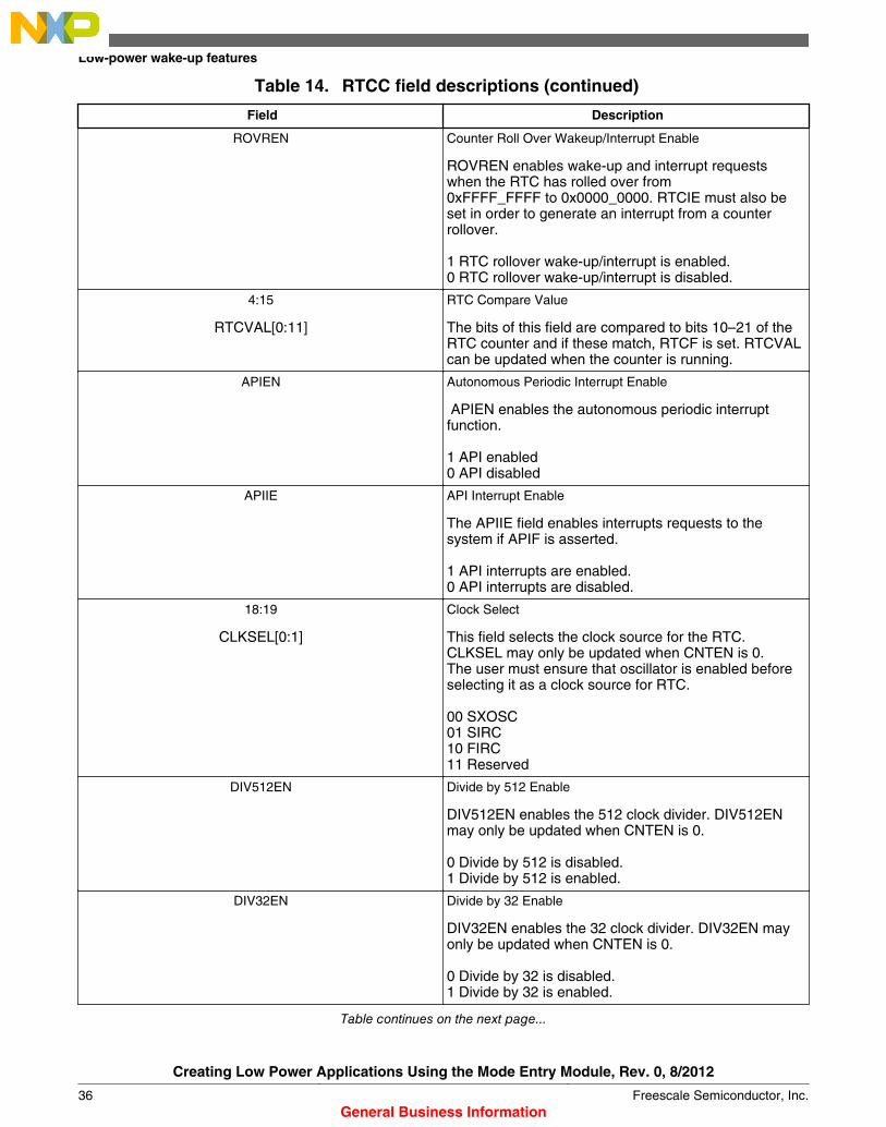
Table 14. RTCC field descriptions (continued)
Field Description
ROVREN Counter Roll Over Wakeup/Interrupt Enable
ROVREN enables wake-up and interrupt requests when the RTC has rolled over from0xFFFF_FFFF to 0x0000_0000. RTCIE must also be set in order to generate an interrupt from a counter rollover.
1 RTC rollover wake-up/interrupt is enabled.0 RTC rollover wake-up/interrupt is disabled.
4:15
RTCVAL[0:11]
RTC Compare Value
The bits of this field are compared to bits 10–21 of the RTC counter and if these match, RTCF is set. RTCVAL can be updated when the counter is running.
APIEN Autonomous Periodic Interrupt Enable
APIEN enables the autonomous periodic interrupt function.
1 API enabled0 API disabled
APIIE API Interrupt Enable
The APIIE field enables interrupts requests to the system if APIF is asserted.
1 API interrupts are enabled.0 API interrupts are disabled.
18:19
CLKSEL[0:1]
Clock Select
This field selects the clock source for the RTC. CLKSEL may only be updated when CNTEN is 0.The user must ensure that oscillator is enabled before selecting it as a clock source for RTC.
00 SXOSC01 SIRC10 FIRC11 Reserved
DIV512EN Divide by 512 Enable
DIV512EN enables the 512 clock divider. DIV512EN may only be updated when CNTEN is 0.
0 Divide by 512 is disabled.1 Divide by 512 is enabled.
DIV32EN Divide by 32 Enable
DIV32EN enables the 32 clock divider. DIV32EN may only be updated when CNTEN is 0.
0 Divide by 32 is disabled.1 Divide by 32 is enabled.
Table continues on the next page...
Low-power wake-up features
Creating Low Power Applications Using the Mode Entry Module, Rev. 0, 8/2012
36 Freescale Semiconductor, Inc.General Business Information
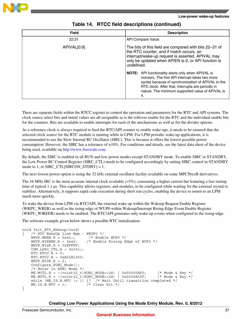
Table 14. RTCC field descriptions (continued)
Field Description
22:31
APIVAL[0:9]
API Compare Value
The bits of this field are compared with bits 22–31 of the RTC counter, and if match occurs, aninterrupt/wake-up request is asserted. APIVAL may only be updated when APIEN is 0, or API function isundefined.
NOTE: API functionality starts only when APIVAL isnonzero. The first API interrupt takes two morecycles because of synchronization of APIVAL to theRTC clock. After that, interrupts are periodic innature. The minimum supported value of APIVAL is4.
There are separate fields within the RTCC register to control the operation and parameters for the RTC and API systems. Theclock source select bits and initial values are all assignable as is the rollover enable for the RTC and the individual enable bitsfor the counters. Bits are available to enable interrupts for each of the mechanisms as well as for the divider options.
As a reference clock is always required to feed the RTC/API counter to enable wake-ups, it needs to be ensured that theselected clock source for the RTC module is running while in LPM. For LPM periodic wake-up applications, it isrecommended to use the Slow Internal RC Oscillator (SIRC). This is because it offers the lowest possible powerconsumption. However, the SIRC has a tolerance of ±10%. For conditions and details, see the latest data sheet of the devicebeing used, available on http://www.freescale.com.
By default, the SIRC is enabled in all RUN and low-power modes except STANDBY mode. To enable SIRC in STANDBY,the Low Power RC Control Register (SIRC_CTL) needs to be configured accordingly by setting SIRC control in STANDBYmode to 1, or SIRC_CTL[SIRCON_STDBY] = 1.
The next lowest power option is using the 32 kHz external oscillator facility available on some MPC56xxB derivatives.
The 16 MHz IRC is the most accurate internal clock available (<5%), consuming a higher current but featuring a fast startuptime of typical 1.1 µs. This capability allows registers, and modules, to be configured while waiting for the external crystal tostabilize. Alternatively, it supports rapid code execution during short run cycles, enabling the device to return to an LPMmuch more quickly.
To wake the device from LPM via RTC/API, the external wake-up within the Wakeup Request Enable Register(WKPU_WRER) as well as the rising-edge of WUP0 within Wakeup/Interrupt Rising-Edge Event Enable Register(WKPU_WIREER) needs to be enabled. The RTC/API generates only wake-up events when configured to the rising-edge.
The software example given below shows a possible RTC initialization:
void Init_RTC_Wakeup(void) /* RTC WakeUp line Mgm - WKUP0 */ WKUP.WRER.R = 0x42;; /* Enable WUP0 */ WKUP.WIREER.R = 0x42; /* Enable Rising Edge of WUP0 */ WKUP.WISR.R = 0xFFFFF; CGM.LPRC_CTL.R = 0x301;; RTC.RTCC.R = 0; RTC.RTCC.R = 0xA01B1000; WKUP.WISR.R = 2; Configure_RUN1_Mode(); /* Enter in RUN1 Mode */ ME.MCTL.R = ((vuint32_t)RUN1_MODE<<28) | 0x00005AF0; /* Mode & Key */ ME.MCTL.R = ((vuint32_t)RUN1_MODE<<28) | 0x0000A50F; /* Mode & Key */ while (ME.IS.B.MTC != 1) /* Wait Until transition completed */ ME.IS.B.MTC = 1; /* Clear bit */
Low-power wake-up features
Creating Low Power Applications Using the Mode Entry Module, Rev. 0, 8/2012
Freescale Semiconductor, Inc. 37General Business Information
To realize a periodic wake-up scenario, the following sequence could be used after the RTC wake-up/ timeout occurred.
if(RTC.RTCS.B.RTCF == 1) RTC.RTCC.R =0; RTC.RTCC.R =0xA01B1000; RTC.RTCS.B.RTCF =1; WKUP.WISR.R = 0x00000002; /* Now, RTC is setup again to allow the next low power mode entry */
9.5 External pin wake-upThe WKPU has several signal inputs that can be used as external interrupt sources in normal RUN mode or as system wake-up sources in all power-down modes.
These external signal inputs include one signal input that can be used as a non-maskable interrupt source in normal RUN,HALT or STOP modes or a system wake-up source in STOP or STANDBY modes. On MPC5607B/C, there is NMI pinconfiguration limitation in STANDBY mode. The NMI pin cannot be configured to generate non-maskable interrupt event tothe core (WKPU_NCR[NDSS] = 00), if the following STANDBY mode is to be used:
• NMI pin enabled for wake-up event• Exit sequence boot from RAM• Code flash module power-down on STANDBY exit sequence
With the configuration given above, the following scenario may occur:• System is in standby.• NMI event is triggered on PA[1].• System wakes up z0 core power domain.• z0 core reset is released and NMI event is sampled by core on the first clock-edge. The z0 core attempts to fetch code at
0x10 address (IVPR is not yet initialized by application) and receives an exception since the flash is not available.
If NMI is configured as wake-up source, WKPU_NCR[NDSS] must be configured as 11. This will ensure no NMI event istriggered on the core but system wake-up is triggered. After STANDBY exit, core will boot and configure its IVOR/IVPR. Itmay then reconfigure WKPU_NCR:DSS to the appropriate configuration for enabling NMI/CI/MCP.
NOTEThe user must be aware that the wake-up pins are enabled in all the modes, therefore, thewake-up pins must be correctly terminated to ensure minimal current consumption. Anyunused wake-up signal input must be terminated using an external pullup or pulldown, orby internal pullup enabled at WKUP_WIPUER. Also, care has to be taken on packageswhere the wake-up signal inputs are not bonded. For these packages, the user must ensurethe internal pullups are enabled for the signals which are not bonded.
void Init_Wake_Up_Inputs(void) SIU.PCR[64].R = 0x103; /* Switch 1 wake-up input - PE[0] = WKUP[6] */ WKUP.WIPUER.R = 0x0003ffff; /* Enable pullups on all 18 wakeup pins */ WKUP.WISR.R = 0x00000008; /* Clear WKUP[6]flag */ WKUP.WRER.R = 0x00000008; /* Enable WKUP[6]for wakeup event */ WKUP.WIREER.R = 0x00000008; /* Enable Rising Edge of WKUP[6] */ /*WKUP.WIFEER.R = 0x00000008; /* Enable Falling Edge of WKUP[6] */ WKUP.WIFER.R = 0x00000008; /* Enable Filter of WKUP[6] */
Low-power wake-up features
Creating Low Power Applications Using the Mode Entry Module, Rev. 0, 8/2012
38 Freescale Semiconductor, Inc.General Business Information
9.6 Wake-up source determinationIn order to allow software to determine the wake-up source at one location, on-chip wake-ups are reported along withexternal wake-ups in the WISR register. Enabling and clearing of these wake-ups are done via the on-chip wake-up source’sown registers. Each external interrupt supports an individual flag which is held in the flag register (WISR). This register is aclear-by-write-1 register type, preventing inadvertent overwriting of other flags in the same register.
9.7 Wake-up interrupt filterThe Wakeup/Interrupt Filter Enable Register (WKPU_WIFER) is used to enable an analog filter on the correspondinginterrupt pads to filter out glitches on the inputs. The number of wake-ups/interrupts supporting this feature is documented inthe relevant reference manual of the specific device of the MPC56xx family, available on http://www.freescale.com, as itvaries across different devices of the MPC56xx family.
NOTEThere is no analog filter for the RTC/API interrupts.
.
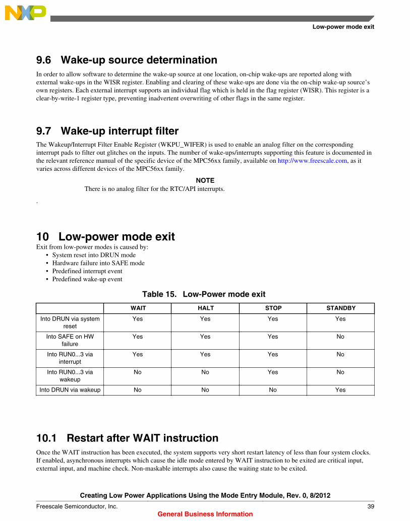
10 Low-power mode exitExit from low-power modes is caused by:
• System reset into DRUN mode• Hardware failure into SAFE mode• Predefined interrupt event• Predefined wake-up event
Table 15. Low-Power mode exit
WAIT HALT STOP STANDBY
Into DRUN via systemreset
Yes Yes Yes Yes
Into SAFE on HWfailure
Yes Yes Yes No
Into RUN0...3 viainterrupt
Yes Yes Yes No
Into RUN0...3 viawakeup
No No Yes No
Into DRUN via wakeup No No No Yes
10.1 Restart after WAIT instructionOnce the WAIT instruction has been executed, the system supports very short restart latency of less than four system clocks.If enabled, asynchronous interrupts which cause the idle mode entered by WAIT instruction to be exited are critical input,external input, and machine check. Non-maskable interrupts also cause the waiting state to be exited.
Low-power mode exit
Creating Low Power Applications Using the Mode Entry Module, Rev. 0, 8/2012
Freescale Semiconductor, Inc. 39General Business Information

10.2 HALT mode exitThe system can exit from the HALT mode by:
• Interrupt• Pin transition• RTC/API timeout
10.3 STOP mode exitUpon exit from STOP mode by pin transition, RTC/API event, or interrupt, only FIRC can be the system clock.
On MPC5607/6/5B/C and MPC5604/3/2B/C, a software timer (SWT) interrupt does not cause STOP mode exit. While inSTOP mode, if the SWT is configured to generate an interrupt and the system clock is disabled (ME_STOP_MC[SYSCLK]= 0xF), a SWT interrupt event will not trigger an exit from STOP mode.
Other internal or external wake-up events such as RTC, API, or WKPU pins, are not affected and will trigger a STOP exitindependent of the ME_STOP_MC[SYSCLK] configuration.
If a SWT interrupt is to be used to wake the device during STOP mode, software may not disable the system clock(ME_STOP_MC[SYSCLK] = 0xF).
In RUNx mode after STOP mode exit, the system RAM can be accessed before it is ready. This is valid only forMPC5604/3/2B/C and if ME_STOP_MC[FXOSC] is enabled, ME_STOP_MC[FIRC] is disabled, ME_RUNx_MC[FIRC] isenabled and ME_RUNx_MC[SYSCLK] = FXOSC or FXOSC_DIV.
At the transition of STOP to RUNx, the RUNx mode can be entered before the system RAM is ready. If the applicationsoftware accesses the RAM during this time, the RAM value cannot be determined.
There are two workarounds possible:• Do not disable the IRC, if the system clock source is not disabled.
The XOSC draws a lot more current than the IRC, so there should be no noticeable increase in the STOP mode powerconsumption.
• Have the software check that the mode transition has completed via the ME_GS register before accessing the systemRAM.
10.4 STANDBY mode exitWhen exiting STANDBY mode by pin transition or timer wake-up, there are two options for code execution depending onthe configuration of RGM_STDBYBOOT_FROM_BKP_RAM:
• System boots from flash on STANDBY exit (reset default)• System boots from backup RAM on STANDBY exit
Configuring system boot from backup RAM has two advantages:• Enables lower power consumption because the flash does not need to be fully powered. Booting from SRAM and
writing C code needs an initialization of the stack pointer and small data areas, which is part of a normal compilerinitialization on reset. However, a smaller code can be written in assembly and has a shorter boot sequence, if bootingfrom SRAM.
• Faster startup time because the flash does not need to be power sequenced.
The amount of power savings when booting from RAM and STANDBY wake-up varies by application.
Low-power mode exit
Creating Low Power Applications Using the Mode Entry Module, Rev. 0, 8/2012
40 Freescale Semiconductor, Inc.General Business Information

NOTEOn exit from STANDBY mode, most of the registers are reset as in a power-up reset.Power domain 0 registers are not reset, including RGM registers, ME _DRUN_MCregister and PCU registers, RTC registers, CAN SAMPLER registers, and so on.
10.4.1 Boot from SRAM after STANDBY exitThe following things must be considered while booting from SRAM after STANDBY exit.
• Make sure the linker file supports code placement in SRAM.• Allow “far calls” by selecting the corresponding compiler option.• Once executing code out of SRAM after STANDBY exit, some CPU registers need to be initialized:
• r1: Initialize stack pointer• r13: Initialize r13 to rw SDA base• r2: Initialize r2 to ro SDA base• r1: Terminate stack
• Call: SRAM_Boot_Function
void Enter_STANDBY_Exit_Into_SRAM(void) /* Configure GPIO[3] */ SIU.PCR[3].R=0x0200; SIU.GPDO[3].B.PDO = 0;
/* Configure GPIO[4] */ SIU.PCR[4].R=0x0200; SIU.GPDO[4].B.PDO = 0; /*Configure WUP3 to exit from STANDBY */ WKUP.WIPUER.R = 0x0003ffff; /* Enable pullups on all 18 wakeup pins (even if by default they are already pulluped) */ WKUP.WISR.R = 0x00000008; /* Clear WUP3 flag */ WKUP.WRER.R = 0x00000008; /* Enable WUP3 for wakeup event */ /*WKUP.WIREER.R = 0x00000008; /* Enable Rising Edge of WUP3 */ WKUP.WIFEER.R = 0x00000008; /* Enable falling Edge of WUP3 */ WKUP.WIFER.R = 0x00000008; /* Enable Filter of WUP3 */ ME.RUNPC[1].R = 0x00000028;/* Peripherals enabled only in DRUN,RUN1 Mode */ ME.LPPC[0].R = 0;/* Peripherals disabled in STOP/HALT/STANDBY Mode */ ME.LPPC[1].R = 0x00002000;/* periphs enabled only in STANDBY Mode */ /*ME.PCTL[72].R = 0x09;/* select the RUNPC1,LPPC1 for EMIOS0 */ Configure_STANDBY0_Mode_SRAM_Exit(); /* Enter in RUN1 Mode */ ME.MCTL.R = ((vuint32_t)RUN1_MODE<<28) | 0x00005AF0; /* Mode & Key */ ME.MCTL.R = ((vuint32_t)RUN1_MODE<<28) | 0x0000A50F; /* Mode & Key */while (ME.IS.B.MTC != 1) /* Wait Until transition completed */ ME.IS.B.MTC = 1; /* Clear bit */
/*Enter in STANDBY Mode */ ME.MCTL.R = ((vuint32_t)STANDBY_MODE<<28) | 0x00005AF0; /* Mode & Key */ ME.MCTL.R = ((vuint32_t)STANDBY_MODE<<28) | 0x0000A50F; /* Mode & Key */ /* Call function located in RAM */
#include "jdp.h"//#include "test.h"//#include "project.h"
//#define FLASH_PD
Low-power mode exit
Creating Low Power Applications Using the Mode Entry Module, Rev. 0, 8/2012
Freescale Semiconductor, Inc. 41General Business Information
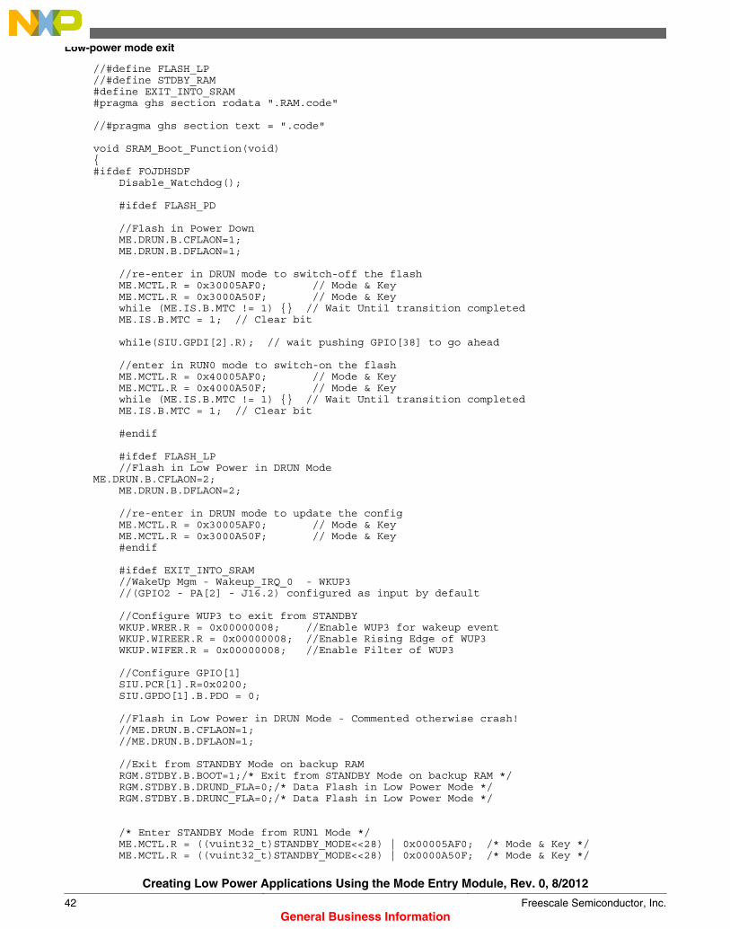
//#define FLASH_LP//#define STDBY_RAM#define EXIT_INTO_SRAM#pragma ghs section rodata ".RAM.code"
//#pragma ghs section text = ".code"
void SRAM_Boot_Function(void)#ifdef FOJDHSDF Disable_Watchdog(); #ifdef FLASH_PD
//Flash in Power Down ME.DRUN.B.CFLAON=1; ME.DRUN.B.DFLAON=1;
//re-enter in DRUN mode to switch-off the flash ME.MCTL.R = 0x30005AF0; // Mode & Key ME.MCTL.R = 0x3000A50F; // Mode & Key while (ME.IS.B.MTC != 1) // Wait Until transition completed ME.IS.B.MTC = 1; // Clear bit
while(SIU.GPDI[2].R); // wait pushing GPIO[38] to go ahead //enter in RUN0 mode to switch-on the flash ME.MCTL.R = 0x40005AF0; // Mode & Key ME.MCTL.R = 0x4000A50F; // Mode & Key while (ME.IS.B.MTC != 1) // Wait Until transition completed ME.IS.B.MTC = 1; // Clear bit #endif
#ifdef FLASH_LP //Flash in Low Power in DRUN ModeME.DRUN.B.CFLAON=2; ME.DRUN.B.DFLAON=2;
//re-enter in DRUN mode to update the config ME.MCTL.R = 0x30005AF0; // Mode & Key ME.MCTL.R = 0x3000A50F; // Mode & Key #endif
#ifdef EXIT_INTO_SRAM //WakeUp Mgm - Wakeup_IRQ_0 - WKUP3 //(GPIO2 - PA[2] - J16.2) configured as input by default //Configure WUP3 to exit from STANDBY WKUP.WRER.R = 0x00000008; //Enable WUP3 for wakeup event WKUP.WIREER.R = 0x00000008; //Enable Rising Edge of WUP3 WKUP.WIFER.R = 0x00000008; //Enable Filter of WUP3
//Configure GPIO[1] SIU.PCR[1].R=0x0200; SIU.GPDO[1].B.PDO = 0; //Flash in Low Power in DRUN Mode - Commented otherwise crash! //ME.DRUN.B.CFLAON=1; //ME.DRUN.B.DFLAON=1; //Exit from STANDBY Mode on backup RAM RGM.STDBY.B.BOOT=1;/* Exit from STANDBY Mode on backup RAM */ RGM.STDBY.B.DRUND_FLA=0;/* Data Flash in Low Power Mode */ RGM.STDBY.B.DRUNC_FLA=0;/* Data Flash in Low Power Mode */ /* Enter STANDBY Mode from RUN1 Mode */ ME.MCTL.R = ((vuint32_t)STANDBY_MODE<<28) | 0x00005AF0; /* Mode & Key */ ME.MCTL.R = ((vuint32_t)STANDBY_MODE<<28) | 0x0000A50F; /* Mode & Key */
Low-power mode exit
Creating Low Power Applications Using the Mode Entry Module, Rev. 0, 8/2012
42 Freescale Semiconductor, Inc.General Business Information
#endif#endif
#pragma ghs section text=default
10.5 Wake-up timingIf the main regulator is also off in device low-power modes, then during the exit sequence, the flash is kept in its low-powerstate and is switched on only when the Main Voltage Regulator Switch-On process has completed.
NOTEAll exit times quoted in the forthcoming sections are from single examples, and must beregarded as typical room temperature values. The time duration may vary slightly fromdevice to device.
10.5.1 Restart after WAIT instructionWAIT mode supports very short restart latency of less than four system clocks.
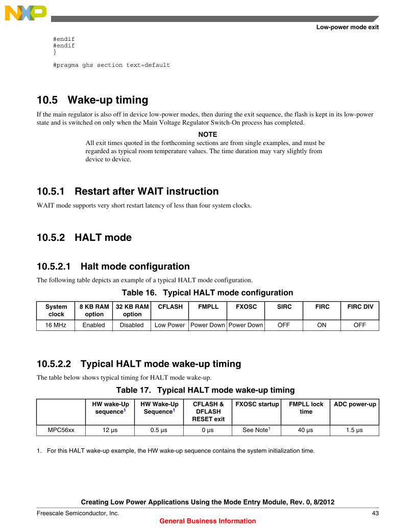
10.5.2 HALT mode
10.5.2.1 Halt mode configurationThe following table depicts an example of a typical HALT mode configuration.
Table 16. Typical HALT mode configuration
Systemclock
8 KB RAMoption
32 KB RAMoption
CFLASH FMPLL FXOSC SIRC FIRC FIRC DIV
16 MHz Enabled Disabled Low Power Power Down Power Down OFF ON OFF
10.5.2.2 Typical HALT mode wake-up timingThe table below shows typical timing for HALT mode wake-up.
Table 17. Typical HALT mode wake-up timing
HW wake-Upsequence1
HW Wake-UpSequence1
CFLASH &DFLASH
RESET exit
FXOSC startup FMPLL locktime
ADC power-up
MPC56xx 12 µs 0.5 µs 0 µs See Note1 40 µs 1.5 µs
1. For this HALT wake-up example, the HW wake-up sequence contains the system initialization time.
Low-power mode exit
Creating Low Power Applications Using the Mode Entry Module, Rev. 0, 8/2012
Freescale Semiconductor, Inc. 43General Business Information
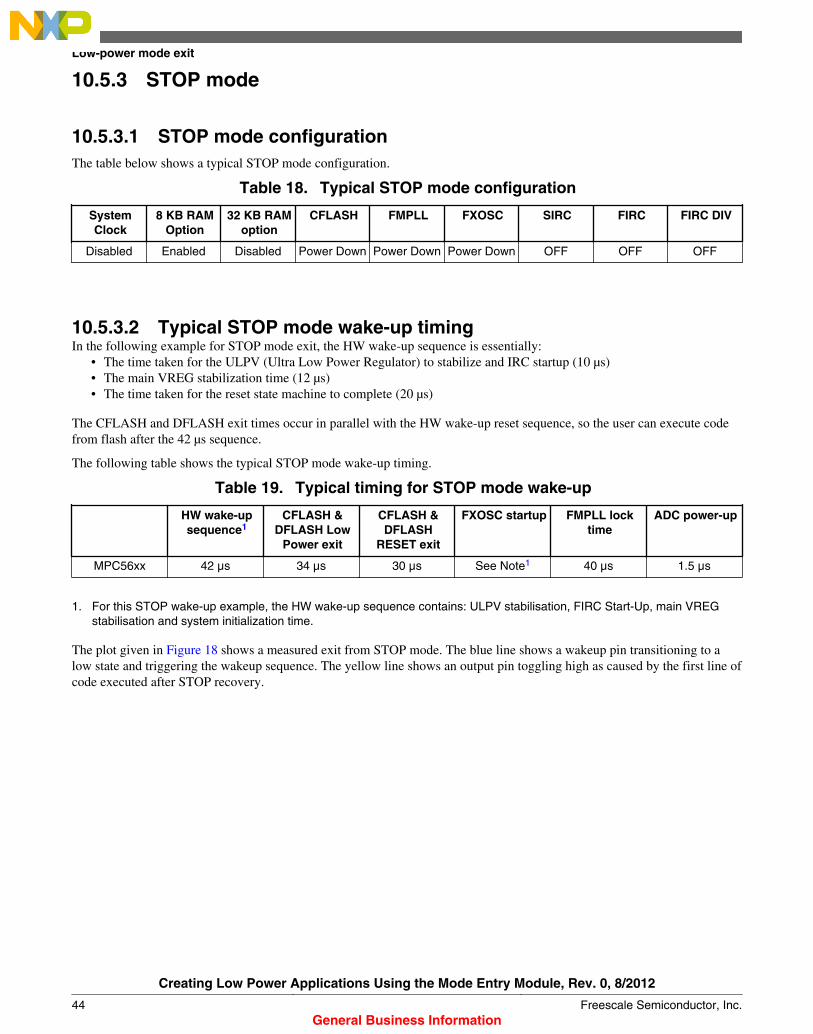
10.5.3 STOP mode
10.5.3.1 STOP mode configurationThe table below shows a typical STOP mode configuration.
Table 18. Typical STOP mode configuration
SystemClock
8 KB RAMOption
32 KB RAMoption
CFLASH FMPLL FXOSC SIRC FIRC FIRC DIV
Disabled Enabled Disabled Power Down Power Down Power Down OFF OFF OFF
10.5.3.2 Typical STOP mode wake-up timingIn the following example for STOP mode exit, the HW wake-up sequence is essentially:
• The time taken for the ULPV (Ultra Low Power Regulator) to stabilize and IRC startup (10 µs)• The main VREG stabilization time (12 µs)• The time taken for the reset state machine to complete (20 µs)
The CFLASH and DFLASH exit times occur in parallel with the HW wake-up reset sequence, so the user can execute codefrom flash after the 42 µs sequence.
The following table shows the typical STOP mode wake-up timing.
Table 19. Typical timing for STOP mode wake-up
HW wake-upsequence1
CFLASH &DFLASH Low
Power exit
CFLASH &DFLASH
RESET exit
FXOSC startup FMPLL locktime
ADC power-up
MPC56xx 42 µs 34 µs 30 µs See Note1 40 µs 1.5 µs
1. For this STOP wake-up example, the HW wake-up sequence contains: ULPV stabilisation, FIRC Start-Up, main VREGstabilisation and system initialization time.
The plot given in Figure 18 shows a measured exit from STOP mode. The blue line shows a wakeup pin transitioning to alow state and triggering the wakeup sequence. The yellow line shows an output pin toggling high as caused by the first line ofcode executed after STOP recovery.
Low-power mode exit
Creating Low Power Applications Using the Mode Entry Module, Rev. 0, 8/2012
44 Freescale Semiconductor, Inc.General Business Information

Figure 18. STOP mode exit
10.5.4 STANDBY mode
10.5.4.1 STANDBY mode configurationThe following table shows the example of a typical STANDBY mode configuration.
Table 20. STANDBY mode configuration
Systemclock
8 KB RAMoption
32 KB RAMoption
CFLASH FMPLL FXOSC SIRC FIRC FIRC DIV
Disabled Enabled Disabled Power Down Power Down Power Down OFF OFF OFF
10.5.4.2 STANDBY mode typical wake-up timingThe following table shows the typical timing for STANDBY mode wake-up.
Table 21. Typical STANDBY mode wake-up timing
HW wake-upsequence1
CFLASH &DFLASH low-
power exit
CFLASH &DFLASH
RESET exit
FXOSC startup FMPLL locktime
ADC power-Up
MPC56xx 787 µs 125 µs 125 µs See Note1 40 µs 1.5 µs
Low-power mode exit
Creating Low Power Applications Using the Mode Entry Module, Rev. 0, 8/2012
Freescale Semiconductor, Inc. 45General Business Information

1. For this STANDBY wake-up example, the HW wake-up sequence contains: ULPV stabilisation, FIRC startup, main VREGstabilisation and system initialization time.
The scope plot given in Figure 19 shows a device in STANDBY mode being wakened by a transition on a wake-up pin (blueline). An output is programmed to toggle at the first available line of code. This will not actually be the first line of code.Since the device was in STANDBY mode, all register content not in PD0 will have had power removed and thus, all registercontent will have been lost. Therefore, the first lines of code will be the initialization code which sets up pins, and modes.
Figure 19. Exit from STANDBY
10.5.5 Wake-Up via RESETThe following figure shows the sequence of events after the internal voltage regulators have stabilized shown by the “power-on RESET” line.
Low-power mode exit
Creating Low Power Applications Using the Mode Entry Module, Rev. 0, 8/2012
46 Freescale Semiconductor, Inc.General Business Information

Figure 20. Typical MPC5604B/C power-on RESET timing
The scope plot below shows the VDD supply going high (blue line) and the RESET pin going high 835 µs later.
Low-power mode exit
Creating Low Power Applications Using the Mode Entry Module, Rev. 0, 8/2012
Freescale Semiconductor, Inc. 47General Business Information

11 Current consumption
11.1 MeasurementsFrom the MPC5604B Microcontroller Data Sheet, available at http://www.freescale.com, typical room temperature values forMPC5604B are as follows:
RUN at 64 MHz = 51mA
HALT (128 kHz IRC running) = 8 mA
STOP (128 kHz IRC running) = 180 µA
STANDBY (128 kHz IRC Running 32 KB RAM ON) = 30 µA
STANDBY (128 kHz IRC Running 8 KB RAM ON) = 20 µA
NOTESee the data sheet for the particular family member being used, available at http://www.freescale.com for typical and maximum values. Always design systems based onthe worst case maximum current.
Current consumption
Creating Low Power Applications Using the Mode Entry Module, Rev. 0, 8/2012
48 Freescale Semiconductor, Inc.General Business Information

12 Common mistakesWhen evaluating new hardware and software, it is not unusual for the users to find themselves unable to achieve the low-power current in the Data Sheet of the particular device of MPC56xx family available at http://www.freescale.com andmeasured on Freescale evaluation boards. Sometimes current even increases at low-temperature instead of the properbehaviour of decreasing. The following checklist has been helpful for bringing up new hardware.
1. Ensure wakeup pins must have either internal or external pullups or pulldowns. If this is not the case, leakage willincrease current. Even if one pin has no internal or external pullups or pulldowns, leakage current will increase. Make alist of all wake-up pins. Check the schematic to determine if an external pullup or pulldown exists. If not, enable weakpullup for that wake-up input in WKPU_WIPUER.
a. Check WKPU_WIPUER bit positions. For example, WKUP0 in MPC5607B has register bit position 31, not 0.
NOTEThe only exception is that when a 32 kHz external oscillator is used, those pinsshould not have these internal pullups enabled.
2. Double check wake-up pins have internal or external pullups or pulldowns.a. Watch out for switched power to pullups/pulldowns. During low-power, wake-up inputs must be either below the
input low-voltage threshold or above the high-input threshold.b. Examine effect of any voltage dividers to wake-up input voltage.c. Make sure resistors on the schematic are populated to wake-up inputs.
3. Ensure TDO pin has pullup or pulldown for STANDBY mode.4. Check the device errata for low-power items
a. For example, the document MPC5607B_1M03Y, Rev. 25 AUG 2011 errata e3242: PB[10], PD[0:1] pinsconfiguration during STANDBY mode. Summary: These pins have both wake-up and analog functionality. Thesignal must be either than 0.2*VDD_HV or higher than 0.8*VDD_HV.
NOTELeaving the debugger connected during low-power will lead to increasedcurrent consumption.
13 Appendix: Debugging with low-power modeBy default, low-power modes shut off as much power as possible, including power to the debugger connection. To preventthe debugger from losing connection, and therefore, possibly asserting a reset, the Nexus Development Interface (NDI)module contains features to maintain a debugger connection. Debuggers may or may not implement this feature.
The controls to maintain the debugger connection are in the Port Configuration Register (PCR) of the Nexus DevelopmentInterface module. These registers are not memory-mapped, and are accessible only through the debugger. Appropriatedebugger scripts must be used to configure these settings.
To maintain a debugger connection, the debugger must set the following:
When exiting STANDBY mode by pin transition or timer wake-up, there are two options for code execution depending onthe configuration of RGM_STDBYBOOT_FROM_BKP_RAM:
• PCRLP_DBG_EN Low Power Debug Enable:
Enables debug functionality to support exit from any low-power mode. Debug functionality is immediately availablefor breakpoints.
When enabled, low-power exit takes longer because the state machine adds steps to wait until after a handshake to thedebugger and the response of the debugger to the handshake is complete.
• PCRMCKO_EN MCKO Enable:
Common mistakes
Creating Low Power Applications Using the Mode Entry Module, Rev. 0, 8/2012
Freescale Semiconductor, Inc. 49General Business Information
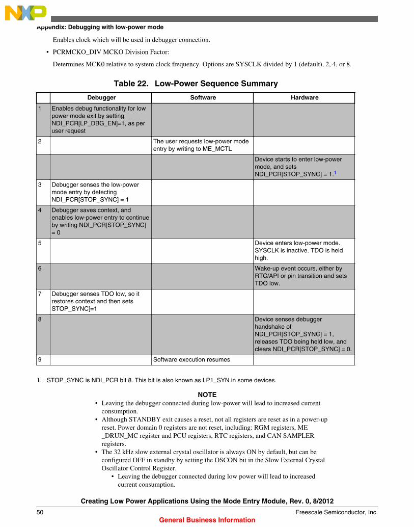
Enables clock which will be used in debugger connection.
• PCRMCKO_DIV MCKO Division Factor:
Determines MCK0 relative to system clock frequency. Options are SYSCLK divided by 1 (default), 2, 4, or 8.
Table 22. Low-Power Sequence Summary
Debugger Software Hardware
1 Enables debug functionality for lowpower mode exit by settingNDI_PCR[LP_DBG_EN]=1, as peruser request
2 The user requests low-power modeentry by writing to ME_MCTL
Device starts to enter low-powermode, and setsNDI_PCR[STOP_SYNC] = 1.1
3 Debugger senses the low-powermode entry by detectingNDI_PCR[STOP_SYNC] = 1
4 Debugger saves context, andenables low-power entry to continueby writing NDI_PCR[STOP_SYNC]= 0
5 Device enters low-power mode.SYSCLK is inactive. TDO is heldhigh.
6 Wake-up event occurs, either byRTC/API or pin transition and setsTDO low.
7 Debugger senses TDO low, so itrestores context and then setsSTOP_SYNC]=1
8 Device senses debuggerhandshake ofNDI_PCR[STOP_SYNC] = 1,releases TDO being held low, andclears NDI_PCR[STOP_SYNC] = 0.
9 Software execution resumes
1. STOP_SYNC is NDI_PCR bit 8. This bit is also known as LP1_SYN in some devices.
NOTE• Leaving the debugger connected during low-power will lead to increased current
consumption.• Although STANDBY exit causes a reset, not all registers are reset as in a power-up
reset. Power domain 0 registers are not reset, including: RGM registers, ME_DRUN_MC register and PCU registers, RTC registers, and CAN SAMPLERregisters.
• The 32 kHz slow external crystal oscillator is always ON by default, but can beconfigured OFF in standby by setting the OSCON bit in the Slow External CrystalOscillator Control Register.
• Leaving the debugger connected during low power will lead to increasedcurrent consumption.
Appendix: Debugging with low-power mode
Creating Low Power Applications Using the Mode Entry Module, Rev. 0, 8/2012
50 Freescale Semiconductor, Inc.General Business Information

• After STANDBY entry, the debugger loses connection to the target due topower gating.
• After STANDBY exit, debugger resync takes longer as the MCU wake-up,that is, the breakpoints won’t be recognized by the debugger, if placed closeto the beginning of the STANDBY exit code.
Appendix: Debugging with low-power mode
Creating Low Power Applications Using the Mode Entry Module, Rev. 0, 8/2012
Freescale Semiconductor, Inc. 51General Business Information
How to Reach Us:
Home Page:www.freescale.com
Web Support:http://www.freescale.com/support
USA/Europe or Locations Not Listed:Freescale SemiconductorTechnical Information Center, EL5162100 East Elliot RoadTempe, Arizona 85284+1-800-521-6274 or +1-480-768-2130www.freescale.com/support
Europe, Middle East, and Africa:Freescale Halbleiter Deutschland GmbHTechnical Information CenterSchatzbogen 781829 Muenchen, Germany+44 1296 380 456 (English)+46 8 52200080 (English)+49 89 92103 559 (German)+33 1 69 35 48 48 (French)www.freescale.com/support
Japan:Freescale Semiconductor Japan Ltd.HeadquartersARCO Tower 15F1-8-1, Shimo-Meguro, Meguro-ku,Tokyo 153-0064Japan0120 191014 or +81 3 5437 [email protected]
Asia/Pacific:Freescale Semiconductor China Ltd.Exchange Building 23FNo. 118 Jianguo RoadChaoyang DistrictBeijing 100022China+86 10 5879 [email protected]
Document Number: AN4240Rev. 0, 8/2012
Information in this document is provided solely to enable system and softwareimplementers to use Freescale Semiconductors products. There are no express or impliedcopyright licenses granted hereunder to design or fabricate any integrated circuits orintegrated circuits based on the information in this document.
Freescale Semiconductor reserves the right to make changes without further notice to anyproducts herein. Freescale Semiconductor makes no warranty, representation, orguarantee regarding the suitability of its products for any particular purpose, nor doesFreescale Semiconductor assume any liability arising out of the application or use of anyproduct or circuit, and specifically disclaims any liability, including without limitationconsequential or incidental damages. "Typical" parameters that may be provided inFreescale Semiconductor data sheets and/or specifications can and do vary in differentapplications and actual performance may vary over time. All operating parameters,including "Typicals", must be validated for each customer application by customer'stechnical experts. Freescale Semiconductor does not convey any license under its patentrights nor the rights of others. Freescale Semiconductor products are not designed,intended, or authorized for use as components in systems intended for surgical implantinto the body, or other applications intended to support or sustain life, or for any otherapplication in which failure of the Freescale Semiconductor product could create asituation where personal injury or death may occur. Should Buyer purchase or useFreescale Semiconductor products for any such unintended or unauthorized application,Buyer shall indemnify Freescale Semiconductor and its officers, employees, subsidiaries,affiliates, and distributors harmless against all claims, costs, damages, and expenses, andreasonable attorney fees arising out of, directly or indirectly, any claim of personal injuryor death associated with such unintended or unauthorized use, even if such claims allegesthat Freescale Semiconductor was negligent regarding the design or manufacture ofthe part.
RoHS-compliant and/or Pb-free versions of Freescale products have the functionality andelectrical characteristics as their non-RoHS-complaint and/or non-Pb-free counterparts.For further information, see http://www.freescale.com or contact your Freescalesales representative.
For information on Freescale's Environmental Products program, go tohttp://www.freescale.com/epp.
Freescale™ and the Freescale logo are trademarks of Freescale Semiconductor, Inc.All other product or service names are the property of their respective owners.
© 2012 Freescale Semiconductor, Inc.