low noise, low power cavity optomechanical oscillators · low noise, low power cavity...
TRANSCRIPT

Low Noise, Low Power Cavity Optomechanical Oscillators
Alejandro GrineMing C. Wu, Ed.
Electrical Engineering and Computer SciencesUniversity of California at Berkeley
Technical Report No. UCB/EECS-2016-180http://www2.eecs.berkeley.edu/Pubs/TechRpts/2016/EECS-2016-180.html
December 1, 2016

Copyright © 2016, by the author(s).All rights reserved.
Permission to make digital or hard copies of all or part of this work forpersonal or classroom use is granted without fee provided that copies arenot made or distributed for profit or commercial advantage and that copiesbear this notice and the full citation on the first page. To copy otherwise, torepublish, to post on servers or to redistribute to lists, requires priorspecific permission.

Low Noise, Low Power Cavity Optomechanical Oscillators
By
Alejandro Joaquin Griñe
A dissertation submitted in partial satisfaction of the
requirements for the degree of
Doctor of Philosophy
In Engineering - Electrical Engineering and Computer Sciences
in the
Graduate Division
of the
University of California, Berkeley
Committee in charge:
Professor Ming C. Wu, Chair Professor Liwei Lin
Professor Constance Chang-Hasnain
Fall 2014

Copyright Alejandro Joaquin Griñe

1
Abstract
Low Noise, Low Power Cavity Optomechanical Oscillators
by
Alejandro Joaquin Grine
Doctor of Philosophy in Electrical Engineering and Computer Sciences
University of California, Berkeley
Professor Ming C. Wu, Chair
Cavity Optomechanical oscillators (OMOs) rely on photon radiation pressure to induce harmonic mechanical motion of a micron-scale light resonator. Unlike most oscillators, optomechanical oscillators require only CW input light without the need for electronic feedback and so hold promise for their novelty. In an optical cavity of sufficient quality factor, the transduction from photons to phonons can be quite efficient as we characterized optomechanical cavities which only required 17 microwatt input optical power to induce mechanical oscillation. The question then remains whether OMOs can be made low noise and of course better yet, low noise and low power. By characterizing various materials and designs, it is shown that indeed OMOs may be made low noise and low power through maximization of the mechanical quality factor – a common quest for MEMs designers. With an emphasis on wafer-scale processes on silicon substrates, OMOs constructed from reflowed phosphosilicate glass, silicon nitride, and silicon were characterized and modeled. Due to non-linear light-matter interactions, OMOs are also known to produce RF frequency combs with an optical carrier. These combs were investigated and a method to produce a frequency comb spanning more than 6GHz from a 52MHz carrier was found. As a demonstration for how an OMO may be utilized in a chip-scale atomic clock, the 9th harmonic of a voltage-tunable device was phase-locked to a low noise microwave reference resulting in an 85dB reduction in phase noise at 1Hz offset from the carrier.

i
Acknowledgements This thesis would not have been possible without the contributions of many, many people too numerous to mention all. My advisor, Ming Wu was always an honest source of knowledge and experience who always told me what I needed to hear. I also greatly appreciate his advice on all non-research matters which especially helped during the writing of this work. Clark Nguyen had never ending optimism and creativity in advising on all aspects of device design and testing. Karen Grutter was in many ways a partner in crime who diligently fabricated and designed most of the devices in this thesis. She helped immensely not only with fabrication but in testing and theory and was a great source of ideas. Turker Beyazoglu fabricated the multimaterial devices and also aided with design and testing. Over the years, he has become a steady friend who lives up to the meaning of his name in Turkey. Always genuine and always kind, I will miss my daily interactions with him. Tristan Rocheleau helped greatly in understanding RF measurements, fabrication and general understanding of optomechanics. He always had an expectation of perfection which was at times difficult to live up to but pushed me to better performance. Niels Quack became a dear friend who helped with initial setup and design and fabrication of silicon devices. Sangyoon Han fabricated the silicon devices and has been a great collaborator. Myung-Ki Kim initially setup the tapered microfiber setup. It was a pleasure to learn from someone who was born with micrometer fingers. Antoine Ramier came on board and tested samples with integrated waveguides. His contribution sparked our interest in the testing and was greatly appreciated. Many undergraduates came on board at different times each helping in different ways. In no particular order they are Inderjit Jutla who helped with automated testing, Eric Zheng who aided with optical Q automation and testing, Scott Li who helped with integrated device testing, and Jeremy Huang tested many high Q samples. Many members of the Nguyen group made contributions including Bobby Schneider, Thura Naing, and Jalal Naghsh. From the Wu group, Michael Eggleston was an excellent source of information in the lab and also provided shelter when I needed it. Philip Sandborn turned in the dissertation paperwork which was a huge favor. I owe a great deal to Sandia National Laboratories for supporting me through this work. Especially Bernadette Montano, who was a constant source of encouragement as the University Programs administrator and my supervisor, Charles Sullivan who pushed me to finish strong and gave me every available resource. Olga Blum-Spahn was an incredible mentor who always made time during her trips to Berkeley to check on progress and give advice. Darwin Serkland, Gary Patrizi, Tom Zipperian, Gil Herrera, and Kent Schubert all aided with the process of joining the DSP program. I must also thank my undergraduate advisor Majeed Hayat who patiently tutored me early on and encouraged me to continue my education. Leslie Kolodziejski and Gale Petrich were outstanding at MIT in teaching me fabrication and optoelectronics. Most of all, this wouldn’t have been possible without my amazing wife, Antonette who never wavered in her support. Fleas, moths, mice, and mold were minor inconveniences compared to being displaced and re-displaced from friends, family, and her business. Yet, she proved savvy, resourceful, and loving through it all. Antonette, I can only repay you with my eternal love. My two kids, Angelina, and Andres have made tremendous sacrifices that I am eternally grateful for. As promised, this thesis is dedicated to Andres. My mother and father, Frances and Alfredo sacrificed so much effort early in my education and continued their support to now. My in-laws Rick and Pauline have been gracious in their support along with Grandma Maggie, and Mickey. I thank the rest of my family and friends for their continued good will and

ii
prayers as well as my past teachers. Without the friendship and prayers of Bay Farm Community Church and the young families group, California would have just been the place I went to school. Finally, thank you God for everyone above, and all the words below.

iii
Table of Contents 1 Motivation .................................................................................................................................... 1
1.1 Organization .......................................................................................................................... 2
2 Whispering Gallery Mode Optical Cavities ................................................................................. 4
2.1 Properties of WGM Cavities ................................................................................................. 4
2.1.1 Optical Quality Factor and Finesse ................................................................................ 8
2.2 Coupled Mode Theory for Ring and Disk Resonators ........................................................ 10
2.2.1 Steady State Solutions.................................................................................................. 12
2.3 Characterization Methods ................................................................................................... 15
2.3.1 RF Intensity Modulation Technique ............................................................................ 19
3 Cavity Optomechanics ............................................................................................................... 23
3.1 Radiation Pressure and the Solar Sail ................................................................................. 24 3.2 Cavity Enhanced Radiation Pressure .................................................................................. 25
3.2.1 Optomechanical Coupling ........................................................................................... 26
3.3 Dynamics of Cavity Optomechanics .................................................................................. 28 3.4 Coupled Mode Equations for Cavity Optomechanics ........................................................ 32 3.5 Large Signal Dynamics ....................................................................................................... 34
3.5.1 Frequency Comb Generation ....................................................................................... 36 3.5.2 Output Power in the hth Harmonic ............................................................................... 37 3.5.3 Carrier Power ............................................................................................................... 43
3.6 Small Signal Dynamics ....................................................................................................... 48
3.6.1 Threshold Power .......................................................................................................... 52 3.6.2 OMO Noise and Phase Noise Spectrum ...................................................................... 57
4 State of the Art Single Material OMO’s: Silicon Nitride and Doped Glass .............................. 70
4.1 Hollow Disk Design and Fabrication .................................................................................. 70 4.2 Tapered Microfiber Pulling ................................................................................................. 72 4.3 Measurement Setup ............................................................................................................. 73 4.4 High Optical Q PSG OMO’s .............................................................................................. 79
4.4.1 Trends with optical Quality factor ............................................................................... 80 4.4.2 Trends with Mechanical Quality factor ....................................................................... 83 4.4.3 Vacuum Setup to Increase Qm ..................................................................................... 83
4.5 PSG with Integrated Waveguides for On-Chip, Low Power Oscillators and RF Combs... 85
4.5.1 Introduction .................................................................................................................. 85 4.5.2 Integrated Waveguide Fabrication and Measurement ................................................. 85

iv
4.5.3 Optomechanical Characterization ................................................................................ 87
4.6 Silicon Nitride as a Low Phase Noise OMO ...................................................................... 89
4.6.1 Low Phase Noise Nitride in Vacuum........................................................................... 90 4.6.2 Frequency Comb Generation ....................................................................................... 91
5 Very Low Threshold Silicon OMO’s ........................................................................................ 93
5.1 Fabrication and Improved Threshold Power Setup ............................................................ 93 5.2 Free Carrier and Non-linear Effects .................................................................................... 98 5.3 Threshold Power with Free Carrier and Nonlinear Optical Effects .................................... 99 5.4 Phase Noise Characterization ........................................................................................... 106
6 Multimaterial OMO Experiments ............................................................................................ 108
6.1 Introduction ....................................................................................................................... 108 6.2 Harmonic Locking to a Microwave Reference ................................................................. 108
6.2.1 Locking Range ........................................................................................................... 112 6.2.2 Long Term Stability Measurement ............................................................................ 114
6.3 High Frequency Harmonic Comb Generation .................................................................. 115
7 Conclusions and Outlook ......................................................................................................... 117 A. S21 Response of a WGM Cavity to Intensity Modulated Light ............................................. 125

1
1 Motivation Cavity optomechanics has emerged as a diverse field which relies on the momentum of
light particles stored in a cavity to alter the mechanical motion of the cavity boundary. Interestingly, by simply changing the wavelength of the light, energy may either be supplied or removed from the one of the cavity mechanical modes. We focus on the former effect where light momentum induces and subsequently amplifies mechanical motion in a self-sustained manner resulting in what is now termed, an optomechanical oscillator (OMO). Originating from the physics community first in the LIGO kilometer-sized cavities [1], followed by studies in glass microtorroids [2], cavity OMOs have now drawn the interest of engineers. Researchers have utilized micro and nano-fabrication to build optomechanical systems of all flavors from photonic crystals [3] and nanobeams [4] to more traditional microdisks [5]. Many of these systems have focused on damping (cooling) rather than amplification (heating) of a mechanical mode partly because initially, OMO’s lacked a killer application. Conversely, cooling a mechanical mode to its quantum ground state and quantum state transfer at micron scales have been recognized as grand challenges surmountable with optomechanics [5–7].
However, applications for OMOs are gaining ground. As a simple, integrated, and low power source of photons modulated at microwave frequencies, OMO’s may find use in mobile optoelectronic applications were low power is a necessity. It is now well known that nonlinear mixing within the OMO results in a frequency comb at the cavity output with comb-lines occurring at harmonics of the mechanical frequency [9][10]. Such non-linear effects may bode well in potential OMO applications including mass sensing [11], microwave photonic downconverters [12], and our focus, as a local oscillator in chip-scale atomic clocks (CSAC). In principle, a high performance OMO stabilized by an atomic transition should yield a lower power CSAC than what is currently available commercially.
First suggested by Rocheleau and Nguyen et al [13], the OMO-integrated atomic clock system is featured below. In the proposed system, the 3.4GHz harmonic of an optomechanically generated frequency comb is locked to the Rubidium hyperfine transition. The uniqueness of the OMO stems from its ability to simultaneously generate the 3.4GHz harmonic and a strong RF tone at tens of MHz comprising the clocks RF output. The OMO would thus replace a microwave synthesizer that is the power hog in the current CSAC clockwork [13]. A lower power CSAC could open up new possibilities in sensing and navigation which require a stable frequency reference.

2
Figure 1.1: Chip-Scale atomic clock with optomechanical local oscillator / frequency divider. The 3.4GHz harmonic of an OMO frequency comb is locked to a Rubidium hyperfine transition which stabilizes the entire OMO frequency comb.
We note that though the given CSAC application may seem narrow in scope, frequency references are everywhere. For instance, the Global Positioning System (GPS) derives position from a measurement of time1 and all GPS satellites are synchronized to atomic clocks. One could only imagine the handy apps that would ensue if our cell phones contained a low power chip-scale atomic clock. In order to compete with current technologies, OMO’s should consume little power, generate many harmonics, have a high signal to noise ratio, and be frequency tunable. This work focuses on the theory and characterization of OMO’s with the goal of meeting the given demands. In oscillators, rather than quoting signal to noise ratio, the most often quoted figure of merit, referred to as phase noise, resembles a noise to signal ratio. Phase noise is thus characterized and modeled in detail. Efforts were focused on whispering gallery mode (WGM), or ring resonator based devices because at the time this work began, they had produced both the lowest phase noise [14] and required the least amount of input power to oscillate [2] albeit, not both simultaneously. Advantageous for high coupling efficiency to fiber and long photon lifetimes, WGM cavity OMO’s have been fruitful in their characteristics during the time of this work. Through modeling and experiments it is shown that mechanical quality factor is a key to achieving both low threshold power and low phase noise, and the WGM design here achieves high mechanical quality factor through design and material choice.
1.1 Organization The thesis begins with an overview of WGM cavities in chapter 2. Optical properties
relevant to cavity optomechanics such as finesse free spectral range and Q are described qualitatively followed by the more quantitative coupled mode theory. Optical characterization methods are briefly described. In chapter 3, cavity optomechanics is introduced and the theory
1 The SI definition of a meter relies on the definition of a second. Formally one meter is defined as the distance light travels in 1/299,792,458 seconds. Meanwhile, one second is defined as the inverse of the Cesium hyperfine transition frequency assumed to be a constant of nature.

3
behind the relative figures of merit is derived. The coupled mode equations for WGM cavities are manipulated in the presence of a movable cavity boundary to derive the power contained in an arbitrary harmonic as well as the OMO carrier power, threshold power, and phase noise. Next, experimental techniques and results of batch fabricated single material phosphosilicate glass (PSG) and silicon nitride OMOs are presented in chapter 0. Silicon nitride is found to yield excellent phase noise spectrum while PSG OMOs demonstrate interesting phase noise characteristics not captured by the simplistic model. Additionally we characterize microwatt-threshold power PSG OMOs fabricated alongside integrated waveguides. In chapter 5, silicon OMO’s are found to demonstrate low threshold power, high mechanical Q and strong phase noise characteristics. We integrate non-linear (self-phase modulation and two photon absorption) as well as free carrier effects into the threshold power model for silicon to reconcile large differences in theoretical and measured threshold powers. In chapter 5, experiments are performed on a multimaterial OMO which demonstrates excellent phase noise and threshold power along with voltage-controlled tuning. As a prelude to locking to an atomic reference, a high order harmonic is phase-locked to a microwave reference and the resulting performance is examined. A method for generating a broadband frequency comb with the multimaterial OMO is introduced.

4
2 Whispering Gallery Mode Optical Cavities Whispering gallery mode (WGM) cavities have utility in various areas of optics including
integrated communication filters [15], optoelectronic oscillators [16], optical modulators/switches [17], cavity quantum electrodynamics (QED) [18], optical frequency comb generation [19] and the focus here, cavity optomechanics [20]. WGM cavities are unique in that they are a proven method to store a vast amount of optical power effectively serving as a passive amplifier for optics. Later, we’ll see that coupling to a WGM may be achieved with a thinned optical fiber or on-chip waveguide. Because many WGM properties are referred to throughout the rest of the thesis, the aspects of WGM resonators pertinent to optomechanics are reviewed.
2.1 Properties of WGM Cavities Light residing in a whispering gallery mode of an optical resonator has a repeating circular trajectory and is guided by successive reflections off the cavity outer periphery rather than an explicit two-dimensional transverse guiding structure. The conceptual ray optics viewpoint of Figure 2.1(a) illustrates light propagating in a whispering gallery mode by repeated bounces off the cavity wall. Light is typically coupled into a WGM using an optical waveguide with judiciously chosen position, dimensions and material. The waveguide optical mode is guided by repeated total internal reflection bounces in the transverse directions as it propagates along the waveguide as illustrated in Figure 2.1(a). Light within the waveguide possesses a non-zero momentum in the lateral (x) direction and thus an evanescent field resides outside the waveguide which carries no time average power unless it couples into the optical cavity. Under the right conditions, the waveguide evanescent field may leak into the resonant WGM – a process known as evanescent coupling. Such a phenomenon is similar to quantum mechanical tunneling by a particle encountering a finite width potential barrier. In this case, the barrier is the low index air between the optical waveguide and resonator.

5
(a) (b)
Figure 2.1: (a) Plan view ray optics illustration for coupling into a whispering gallery mode from a waveguide. (b) Cross-sectional view of the waveguide and WGM resonator at the point of minimum distance between the two. Drawn in red are the unperturbed normalized transverse optical field profiles of the waveguide and cavity.
Several mathematical models and simulation tools exist which predict the coupling efficiency from the optical waveguide to the WGM and are well explained by other sources [6–8]. Summarized below are the important results of the mathematical treatment:
• Orthogonal TE and TM modes: The WGM cavity has natural cylindrical symmetry and thus can be solved with a cylindrical ( ˆ ˆ ˆr, ,zϕ ) set of Maxwell’s equations for the resonant (allowed) optical modes. Assuming a dielectric cavity of height, h constructed out of dielectric material with refractive index cavn , the modes can be approximately resolved
into two orthogonal polarizations except in very thick cavities satisfying / 2 cavh nλ>> , where λ is the wavelength of interest. In the “thin cavity” approximation, the z component of the field k-vector must then be small compared to the in-plane k-vector in order for total internal reflection to occur at the cavity top and bottom faces. The two orthogonal polarizations satisfying Maxwell’s equations with appropriate boundary conditions are then:
o Quasi TE polarized modes having dominant , ,r zE E Hϕ field components and,
o Quasi TM polarized modes having dominant ,H ,Er zH ϕ field components.
Here, E and H are the electric and magnetic fields respectively. The optical waveguide in Figure 2.1 follows a similar convention with TE polarization having dominant
, ,x y zE E H components and TM polarization with dominant ,H ,Ex y zH components. In both waveguides and resonators, TE modes tend to be more confined, and thus occupy a smaller mode volume than TM modes.

6
• Resonant Wavelength: The cavity guided modes (eigen-modes) are categorized as either
, ,p mTE
or , ,p mTM
where the subscripts p,m, are integers representing the number of field antinodes in the radial ( r ), azimuthal (ϕ ), and vertical ( z ) directions respectively. Ring and disk-shaped cavities can support modes with a single antinode in the radial and vertical directions such that , 1,2...p = while the periodic boundary condition in the
azimuthal direction requires 2 1ik Re ϕ π= or,
k R mϕ = (2.1)
so that m is also a non-zero integer counting the number of azimuthal node/antinode pairs.R is the cavity radius, and kϕ is the wave-vector magnitude in the ϕ direction.
Defining the effective index /eff o cn c kϕ ω≡ , as the ratio of the vacuum speed of light oc
to the ϕ phase velocity for the mode of interest, the cavity resonant frequency is found from (2.1),
/o eff
c
c nm
Rω = (2.2)
Since cω is assumed to be measured in free space, the corresponding free-space wavelength obeys the dispersion relation,
2 o
cc
cπω
λ= (2.3)
Substitution into (2.2) gives,
2 /c effR m nπ λ= (2.4)
which is written to emphasize that at resonance, an integer number of effective wavelengths fit around the circumference. In general, larger m implies more node/antinode pairs along ϕ , larger (i.e. more glancing) reflection angle at the cavity wall and thus greater likelihood for total internal reflection. Typically 8m > at telecommunication wavelengths even for very small cavities. For instance, a very small
1R mµ= AlGaAs cavity demonstrated a resonant wavelength of 1438nm for the
1, 9, 1TEp m= = = mode [24].
• Free Spectral Range: The free spectral range (FSR) is the frequency or wavelength spacing between adjacent cavity modes with successive azimuthal mode numbers i.e.
1m∆ = ± . Taking /dm dω in equation (2.1), setting 1dm m≈ ∆ = and solving for
FSRdω ω= ∆ gives,
/o g
FSR
c nR
ω∆ = (2.5)

7
The group index is defined as the ratio of the vacuum speed of light to the group velocity,
/g o gn c v≡ with ( ) 1/gv dk dϕ ω
−= . Again, the FSR is measured in free space so (2.3)
applies and thus 2/ 2 /c
o cd d cλ
ω λ π λ= . Substitution into (2.5) with d → ∆ gives,
2
2c
FSRgRn
λλ
π∆ = (2.6)
The FSR scales inversely with the cavity radius and refractive index. Since each mode has a different group index, the FSR is not the same for all modes.
• Coupling Gap: To couple adequate optical power into the WGM, the evanescent portion of the transverse waveguide mode, ( , )guideU x z must partially overlap the resonator as shown in Figure 2.1(b) where a small yet critical tail of the waveguide evanescent field penetrates the resonator material. The capability for efficient coupling is quantified in the coupling coefficient, mc given by,
( )*1/2m guide cavc E E dV∝ ∫
(2.7)
which shows that the waveguide field must overlap the resonator field for coupling. Such a condition is met by careful placement of the waveguide with respect to the resonator, and by fabricating a waveguide with sufficiently small lateral width for an adequate evanescent field.
• Critical Coupling: A smaller gap will lead to a larger single pass coupling coefficient,
mc (i.e. treating the resonator as a finite length waveguide over the interaction length) [21]. However, a smaller coupling gap and hence more evanescent field overlap doesn’t necessarily lead to the most resonant dropped power drop in outP P P= − when considering the phase shifted field the resonator returns back to the waveguide upon each round trip [21]. In fact, the most dropped power occurs at an intermediate gap distance referred to as the critical coupling point which will be treated in the upcoming section. Once the coupling gap exceeds the critical coupling point, the amount of coupled or dropped power is reduced exponentially as the gap increases.
• Phase Matching: So far, we have seen that for efficient waveguide to resonator coupling, the light launched in the waveguide should closely (in the next section we will investigate how close) match the resonant wavelength, cλ and the coupling gap should be carefully chosen. A third condition deemed “phase matching” requires that the field in the waveguide remain in phase with the field in the resonator over the effective interaction region. Phase matching is accomplished by equating the respective waveguide and resonator propagation k-vectors in the effective index approximation.
2 /guideguide eff onβ π λ= (2.8)
2 /cavcav eff cnβ π λ= (2.9)

8
Here, guideeffn and cav
effn are the effective index of the waveguide and resonator respectively
while oλ is the vacuum wavelength of light launched into the waveguide. Phase matching is understood by expanding the electric fields in equation (2.7) to yield,
( )1/2 ( , )U ( , ) .cav guidei ym guide cavc U x z x z e dVβ β−
∝ ∫ (2.10)
( , )guideU x z and ( , )cavU x z are the unperturbed transverse mode profiles of the waveguide and resonator. Due to the oscillatory nature of the integrand in equation (2.10), coupling is only possible if guide cavβ β≈ or assuming o cλ λ≈ in equations (2.8) and (2.9),
guide caveff effn n= . A strategy for meeting the phase matching condition can be ascertained
from the dispersion relations in the waveguide and resonator.
2 2 2 2 2guide guide o x zn k k kβ = − − (2.11)
2 2 2 2cav cav on k kβ ⊥= − (2.12)
Where ok is the free space wavenumber (2 / oπ λ ) while guiden and cavn are the
refractive index of the bulk waveguide and resonator materials respectively. xk and zk are the x, and z components of waveguide k-vector while k ⊥ is the transverse k-vector of the cavity effective waveguide in the interaction region consisting mostly of r and z components. Equating (2.11) and (2.12) leads to the conclusion that phase matching is readily achieved by designing the waveguide and resonator to have similar materials and transverse mode profiles.
2.1.1 Optical Quality Factor and Finesse Light propagating in a cavity has a finite lifetime due to various loss mechanisms which
couple the cavity to non-resonant modes. The capability of the cavity to store light is quantified in the optical quality factor defined for any resonant system as the number of cycles light is stored in the cavity,
/
totdiss cycle
UQU
= (2.13)
Where U is the total stored energy in the mode of interest and the denominator is the average energy dissipated per optical cycle having period 1( / 2 )cω π − . Assuming a total cavity photon
lifetime, cτ the rate of energy decay is / / cdU dt U τ= − with units [Joules/s] so that the
average energy dissipated in one cycle is 1/ ( )diss cycle c cU Uω τ −= and thus
ctot c cQ
ωω τ
κ= = . (2.14)

9
The second relation in equation (2.14) is derived by taking a Fourier transform of the time dependent photon decay, ( )U t yielding a spectrum ( )U ω in radial frequency space having a value of κ for the full width half max (FWHM) which equals the cavity photon decay rate. Since the various photon loss mechanisms act in parallel, the total decay rate in cyclical frequency units [cycles/sec] is the additive sum of each loss source
rad abs scat ex o ex hotκ κ κ κ κ κ κ κ= + + + = + + . (2.15)
Where radκ , absκ , scatκ , exκ , oκ , and hotκ are the radiation, absorption, scattering, external, intrinsic, and “hot” decay rates respectively. Substitution of (2.15) into (2.13) allows one to explicitly write the total or “loaded” optical quality factor,
1 1 1 1 1 1 1 1tot rad abs scat ex o ex hotQ Q Q Q Q Q Q Q− − − − − − − −= + + + = + + (2.16)
where the thi component of the total optical quality factor originating from decay rate component, iκ is /i c i c iQ ω τ ω κ= = . The various loss components in equation (2.16) are summarized below:
• radQ : Radiation loss, also known as bending loss arises from non-total internal reflection (TIR) within the circular cavity. Radiation loss is more severe for small cavity radii and lower order (longer cλ ) azimuthal modes since these conditions reduce the chance for TIR.
• absQ : Linear optical absorption arises from single photon loss events such a defect, free carrier or conventional inter-band absorption. Surface states due to residual etch byproducts [25], or chemical adsorption [26] can also contribute to single photon absorption. Multiphoton or nonlinear effects such as two photon absorption are captured in hotQ further explained later. The various absorption mechanisms are further studied for silicon micro-resonators in chapter 5.
• scatQ : Rough surfaces due to imperfect etching as well as inhomogeneous bulk material contribute to the scattering decay rate which scales with the modal field overlap with an imperfect surface. Thus, higher radial order TE modes exhibit smaller surface scattering rates and larger scattering limited Q’s.
• exQ : Often regarded as the coupling Q, exQ accounts for deliberate loss to an externally coupled waveguide.
• oQ : The intrinsic or “cold cavity” Q is limited to optical loss internal to the resonator that
is independent of the circulating power. Loss rates included in oκ are assumed to retain their same value regardless of the stored cavity photon number and are thus time independent.
• hotQ : The third term in equation (2.15), hotκ accounts for nonlinear and time varying loss components such as two photon absorption which depends on the instantaneous photon number. Single photon absorption that depends on electrical carriers may also contribute
10
to hotκ since the carrier number may depend on the photon number, especially if two photon absorption is relevant or the cavity is electrically pumped. This component will be ignored throughout the thesis and is only visited in the context of silicon resonators.
The modal loss, Im kα = − can be written in terms of totQ by noting the fraction of modal
energy dissipated due to loss is, /diss
dU dx Uα= − . Substituting gdx v dt= where /g o gv c n=
is the group velocity and use of (2.14) gives,
o
g c totdiss
cdU U UU Udt n Q
α κ ωτ
= − = − = − = − (2.17)
1 2,/
go ctot
g o g c
ncQ
n c nω πκ α
α α λ→ = = = (2.18)
Routinely mentioned in the context of optical resonators is the cavity finesse defined as,
/o gFSR
c nR
ωκ κ
∆≡ = (2.19)
where equation (2.6) was utilized for FSRω∆ . Noting that the average number of cavity round
trips a photon makes prior to decaying is given by the ratio of the distance traveled in time cτ to the circumference we find,
/ /1 1#
2 2 2c o g o gc n c n
round tripsR R
τπ π κ π
= = = (2.20)
The number of round trips which depends on both the cavity radius and quality factor is thus intimately related to the finesse.
2.2 Coupled Mode Theory for Ring and Disk Resonators So far, the properties of WGM resonators have been summarized and important figures of
merit such as the optical quality factor and finesse have been defined. It was mentioned in section 2.1 that the input light need not be exactly on resonance in order to couple power into the resonator. In this section we derive the transmission of a circularly shaped optical resonator as a function of the difference in frequency between the input light and cavity resonant frequency. Coupled mode theory [27] along with the intuitive nomenclature of [28] is utilized.
We begin by assuming the resonator is pumped with coherent light such as that available from a laser with output radial frequency oω . The field within the cavity is then written in
complex phasor notation, ( , ) Re ( ) ( ) oi tcav cavE r t u r a t e ω−=
where ( )cavu r accommodates the

11
fields spatial and polarization properties while the complex mode amplitude, ( )a t tracks any
temporal transients other than the assumed oi te ω− dependence. It is convenient to normalize so
that 2
( )a t gives the number of photons occupying the mode of interest with stored energy, 2
( )oU a tω= . The field within the waveguide at the coupling junction is written,
( , ) Re ( ) ( ) oi tguide guide inE r t u r s t e ω−=
and is conveniently normalized such that 2
( )ins t is the
photon arrival rate at the waveguide-cavity coupling junction. A similar notation is followed for ( )outs t , the field exiting the waveguide-cavity coupling junction.
The system described above is illustrated in Figure 2.2 which shows a fraction of the launched waveguide field at frequency oω entering, and then exiting the cavity with external
angular coupling rate, exκ . The cavity resonant frequency is cω and the total cavity decay rate including deliberate loss to the waveguide, is κ . All rates are in angular units [rad/s].
Figure 2.2: Dynamical variables involved in the coupled mode theory and relation to the described time constants, decay rates, and frequencies of interest.
The dynamical complex variables, ( )ins t , and ( )a t then obey,
( ) ( ) ( )e2
oi tc in exa t i a t s t ωκω κ−
= − − +
(2.21)
( ) ( )e ( )oi tout in exs t s t a tω κ−= − (2.22)
Assuming a reference frame rotating at laser field angular rate oω yields with
( ) ( ) oi ta t a t e ω−→ and ( ) ( ) oi ts t s t e ω−→ ,
( ) ( ) ( )2 in exa t i a t s tκ κ
= ∆ − +
(2.23)
( ) ( ) ( )out in exs t s t a t κ= − (2.24)

12
o cω ω∆ ≡ − (2.25)
The detuning, defined in (2.25) is positive for input light blue shifted from resonance ( o cω ω> ,
o cλ λ< ) and negative for red detuning ( o cω ω< , o cλ λ> ). In contrast to Fabry-Perot resonators,
( )outs t was defined positive for output light propagating the same direction as ( )ins t .
2.2.1 Steady State Solutions If ( )ins t is constant in time, then ( ) 0a t = , and we can solve for the steady state version of the otherwise dynamical variables to yield,
/ 2
exina s
iκ
κ=
− ∆ + (2.26)
1/ 2
exout in ex ins s a s
iκ
κκ
= − = − − ∆ +
(2.27)
where the over-bars indicate steady state. The stored energy in the cavity is found from (2.26) and the previously assumed normalizations for ( )a t and ( )s t ,
( )
222
| ( )|/ 2
exo inU a t P
κω
κ= =
∆ + (2.28)
A Lorentzian peak with FWHM given by κ and energy on resonance of 2( 0) 4 /in exU P κ κ∆ = = . Equation (2.27) gives the steady state field transmission ( )T ∆ for a WGM cavity,
( ) 1/ 2
out ex
in
sT
s iκ
κ∆ ≡ = −
− ∆ + (2.29)
Likewise, the ratio of output to input power in the waveguide is the cavity optical power transmission,
( )
( )
22 22
2 22
/ 2( )
/ 2exout
in
sT
s
κ κ
κ
∆ + −∆ = =
∆ + (2.30)
Which is Lorentzian dip of FWHM width κ . Equation (2.30) shows that cavities with longer lifetime are less tolerant of input radiation away from resonance as these frequencies are not dropped by the cavity and are allowed to pass through the waveguide. Physically, the longer lifetime means light of a frequency not meeting the resonant condition of (2.2) survives long enough in the cavity to eventually destructively interfere with itself erasing the circulating power on a timescale of ~ 2/κ . Often, one is interested in measuring the intrinsic quality factor, oQ

13
-3 -2 -1 0 1 2 3
0.0
0.2
0.4
0.6
0.8
1.0
0.1 0.25 0.5 0.75 0.9
Powe
r Tra
nsm
issio
n
Normalized Detuning: ∆/κo
Qtot/Qo
from samples of the total quality factor totQ . Using equations (2.14) and (2.15) and ignoring hotQ, we can eliminate exκ to recast equations (2.28) and (2.30) in a more lab-specific form,
22 2 2
2
1 1| |
2 2
c tot
tot o oino in
oc
tot o o
QQ Q P
U a P
Q
ω κκ
ωκω κ
κ κ
− −
= = = ∆
∆ + +
(2.31)
2 22 2
2
2
2 2 2
2
1 12 2
( ) .
2 2
c tot
tot o o o
c
tot o o
QQ Q
T
Q
ω κκ κ
ω κκ κ
∆∆ + − + −
∆ = = ∆
∆ + +
(2.32)
The normalized detuning, / oκ∆ was introduced for graphing convenience. Both the Lorentzian stored cavity energy and inverse Lorentzian power transmission are plotted vs. normalized detuning in Figure 2.3. The stored cavity energy on resonance is proportional to in oP Q and is
greatest when the detuning, 0∆ = , and coupling ratio, / 2oκ κ = .
-3 -2 -1 0 1 2 3
0.0
0.2
0.4
0.6
0.8
1.0 0.1 0.25 0.5 0.75 0.9
Norm
alize
d Ca
vity
Ene
rgy:
κoU
/Pin
Normalized Detuning: ∆/κo
Qtot/Qo
(a) (b)
Figure 2.3: (a) Stored cavity energy multiplied by /o inPκ plotted vs normalized detuning for different coupling ratios from equation (2.31). (b) Power transmission through a coupling waveguide vs normalized detuning parameterized by the coupling ratio from equation (2.32).
Setting the derivative of (2.31) equal to zero shows that the stored energy is largest when / 2tot oQ Q= or 2 oκ κ= which is defined as the critical coupling point. On resonance, and at

14
critical coupling, we find the maximum stored energy, max /in oU P κ= and dividing by the round
trip time, rtτ the maximum circulating power is,
max,
/.o g
circ max in inrt
c nUP P P
Rτ π κ π= = =
(2.33)
Equation (2.19) was substituted for the finesse. Note that , /circ max inP P is a factor of two larger than the average round trips calculated in (2.20) which didn’t account for the constant supply of photons entering through the external waveguide. The probability for a circulating photon to eventually couple into the waveguide is /( )ex ex oκ κ κ+ which varies from zero to one and is exactly 1 / 2 at critical coupling. It is evident from the power transmission of equation (2.32) and Figure 2.3(b) that on resonance at critical coupling, the transmitted power is zero. Hence, the probability for an input photon to couple into the cavity is 21 | ( 0)| 1T− ∆ = = . At critical coupling, one then concludes that twice as much power enters the cavity through the waveguide as leaves it through the waveguide. The ratio of circulating power to input power is then enhanced by a factor two due to waveguide coupling. Coupling Regimes Three distinct coupling regimes are apparent in Figure 2.3
• Critically Coupled / 2tot oQ Q= ( 2 ok κ= ) : We have already discussed critical coupling and its importance as the gap width which maximizes the intracavity power. Due to destructive interference between ins and the phase shifted field leaking into the waveguide from the resonator, both the transmitted field and power are zero on resonance at critical coupling. In reality, due to noise and imperfect phase and polarization matching, the transmission never reaches exactly zero but extinction ratios on the order of 20dB are readily achievable. The intrinsic Q is also conveniently measured at critical coupling since it can be calculated from the measured linewidth. i.e.
,2 / 2 /o c crit c FWHM critQ ω κ λ λ= = ∆ . To use this method, the coupling gap and polarization would be adjusted until the deepest transmission dip is obtained.
• Overcoupled / 2tot oQ Q< ( 2 oκ κ> ): When the coupling gap is smaller than the critically coupled point, the cavity loses energy to the waveguide at a rate that exceeds the intrinsic cavity loss rate, oκ . This overcoupled regime is handy for locating otherwise narrow lineshapes which are broadened for small coupling gaps as seen in Figure 2.3(b). At high enough coupling rates the transmission resonances are difficult to discern from the noise since the transmission dip is shallower.
• Undercoupled / 2tot oQ Q> , ( 2 oκ κ< ): In this regime the external coupling rate is small resulting in the least amount of waveguide loading. The intrinsic Q is recovered in this regime since for large enough coupling distances, 0exκ and thus the measured
linewidth is oκ κ . As seen in Figure 2.3(b) when the resonant transmitted power is

15
about 70% of the input power, the measured total Q is 90% of the intrinsic Q. Further retracting the waveguide, would produce 80% resonant power transmission when the measured Q is 95% of the intrinsic Q. Of course, in this regime, the lineshape is both narrow and shallow and may thus be difficult to resolve or discern from the noise. For this reason, it is typical to locate a resonance when overcoupled, increase the coupling gap, reduce the measurement bandwidth, and then extract the intrinsic Q while undercoupled.
2.3 Characterization Methods Although the focus of this work is on cavity optomechanical oscillators, substantial effort
was spent on characterizing the passive optical properties of various materials, cavity designs, and fabrication splits. In all, more than 300 devices of various shapes, sizes and materials were optically characterized. Over time, the optical Q measurement turnaround time and resolution improved and it is worth reviewing the characterization methods investigated in this work. Summarized in Figure 2.4 are the optoelectronic characterization setups for each characterization method and the expected measurement trace. Light can couple into the device from an integrated waveguide or tapered microfiber - a thinned fiberoptic cable further described in section 4.2. The tapered microfiber can be mounted on nano-positioning piezo stages to control the orientation and gap distance. In each method, the intrinsic Q can be ascertained from the undercoupled response, or by choosing a gap distance corresponding to critical coupling where the intrinsic Q is easily extracted from the total Q measurement. The coupling is controlled by either choosing an integrated waveguide with appropriate gap or in the tapered fiber case, by gradually moving the tapered microfiber until the desired coupling is achieved.

16
(a) (b)
(c) (d)
Figure 2.4: Methods and measurement setups for characterizing the optical properties of ring microresonators. (a) Swept laser technique. The tunable laser center frequency is chirped in time and the microresonator response is captured by an oscilloscope. (b) Ring down spectroscopy. A stationary or chirped tunable laser is intensity modulated while recording the time required for the cavity to dissipate energy on an oscilloscope. (c) Broadband or white light spectroscopy. Light from a broadband source is sent through the cavity and recorded with an optical spectrum analyzer or spectrometer. (d) Intensity Modulation Spectroscopy. Setup implemented in this work utilized an intensity modulated stationary tunable laser. A network analyzer sweeps the RF modulation frequency while recording the cavity response.
Swept Laser Technique Likely the most common technique for characterizing the optical Q and FSR, this technique relies on a tunable laser with continuous or well controlled discrete tuning capability. As illustrated in Figure 2.4(a), the laser wavelength is swept while a photocurrent captures the cavity transmission on an oscilloscope. We controlled polarization with a fiber bench incorporating a free space polarizer aligned to the laser followed by a half-wave plate. The free space system was more deterministic and repeatable than a paddle wheel polarization controller. Figure 2.5 gives representative measurements from a high finesse 52.5μm radius free standing phosphosilicate glass (PSG) ring resonator fabricated alongside integrated waveguides. This device posted a Q of 4 million, an FSR of 5nm and thus a finesse of ~13k. Note that a separate group reported an integrated waveguide silica device smoothed by laser reflow exhibiting a similar Q of 3.2 million at 1550nm [29]. Though it wasn’t given for the particular highest Q device, a best case estimate for the FSR is 7.9nm which yields a similar finesse of 16 thousand.

17
1550.700 1550.702 1550.704 1550.706 1550.708
0.50
0.55
0.60
0.65
0.70
0.75
0.80
0.85
Raw Fit
Powe
r (µW
)Wavelength (nm)
Qtotal=3.9M
In chapter 4, we will explore the characterization of optical resonators with integrated waveguides in more detail.
1549 1550 1551 1552 1553 15540.4
0.5
0.6
0.7
0.8
0.9
1.0
1.1
Tran
smiss
ion
(A.U
.)
Wavelength (nm)
(a) (b)
Figure 2.5: Measured spectra of 52.5μm Phosphosilicate glass ring resonator coupled to an integrated waveguide measured with a continuously swept laser. (a) Wide sweep covering the 5nm FSR. To record such a wide span with adequate resolution three separate scans of 10,000 points each were stitched together. (b) Zoom of resonance at 1550.7nm taken with a narrower wavelength sweep range.
To convert from oscilloscope time stamps to wavelength, either the laser chirp rate must be calibrated, or an optical element of known frequency response may be measured simultaneously to map time to wavelength. A calibrated Mach Zender serves this purpose well [30]. We instead chose to validate the laser sweep rate by comparing the measured linewidth to that obtained from the intensity modulation method of Figure 2.4(d) described later.
Early optical Q measurements utilized a LabVIEW-controlled discrete laser frequency sweep where the laser was stepped in intervals as small as 0.1pm – the limit of our HP 81682A laser module. An HP 8153A power meter was used to record the power at each step. However, once the optical Q exceeded 5 million ( 0.3pmFWHMλ∆ = ) in standalone devices, 0.1pm was not enough resolution. We then switched to a continuous laser sweep and connected the analog output of the 8153A power meter to an Agilent TDS 3054 oscilloscope. The oscilloscope trigger was provided by the tunable laser configured to output a pulse at the beginning of each sweep. Care was taken to avoid capturing artificial resonances caused by ringing of the laser during the backwards sweep at the termination of each cycle. Since the 8153A power meter changes sensitivity at predefined input powers, we chose to operate it in manual sensitivity mode and queried the operator for the input power prior to initiating a sweep. All operations were automated with LabVIEW. The continuous sweep proved significantly faster than discrete sweep since LabVIEW is only called at the beginning and end of each wavelength ramp.
Though the swept source method is rapid, and has laser linewidth-limited resolution, deeply undercoupled cavities are difficult to detect in a large span because a small dip in power must be discerned from the background noise. To avoid thermal distortion of the measured

18
spectrum [31], the laser power must be kept small, often in the 100nW range, hindering the signal to noise ratio. We observed the noise to be dominated by changes in the laser output power during the sweep. The RF Intensity modulation method doesn’t suffer the same drawback since the laser frequency is kept constant, and the laser threshold power to induce thermal distortion is larger.
Cavity Ring Down Cavity ring down has previously been applied to measure ultrahigh Q WGM resonators in various materials including a 5.5mm diameter CaF2 resonator with a Q of 6 x 10¹⁰ at 1064nm [32]. This method is particularly useful since it is not limited by the laser linewidth and is immune to thermal skewing of the Q [33]. In order to implement the method, a laser is tuned to the WGM then abruptly switched off to view the lifetime, /c tot cQτ ω= of stored cavity energy. The thermorefractive effect typically aids in broadening the optical resonance (without affecting the cavity lifetime) to allow easy alignment with the laser. An exponential fit of the output power to the equation, /( ) ( ) ct
out oP t P P e Pτ−∞ ∞= − + yields totQ as shown below for a 52.5μm PSG disk
with fitted optical Q of 1.9M at critically coupled and thus an intrinsic Q of 3.8M.
0 1 2 3 4 51.55
1.60
1.65
1.70
1.75
1.80
1.85
No Cavity Critically Coupled Fit after 2.25ns
Volta
ge
Time (ns)
Figure 2.6: Ring down measurement of a 52.5μm PSG disk resonator. The critically coupled decay trace (blue) was fitted (red) after the ~2ns fall time of the driving electronics (black).
The data in Figure 2.6 was obtained by feeding a square wave to an intensity modulator whose optical output was launched into a critically coupled cavity. Ring down is impractical for low-Q cavities as the decay time becomes shorter than the fall time either producible or measurable from the associated electronics. We used an SRS DG535 pulse generator connected to an OPT-40B pulse inverter to produce signals with ~2ns fall time. The black curve in Figure 2.6 shows the output transient when the laser is off resonance with the cavity reaching the baseline power after 2ns. To fit the curve when coupled to the cavity, we began the fit after 2.25ns and enforced the voltage at t=0 to be 1.78 volts.
Broadband Source

19
Similar to using a swept laser, the broadband source technique of Figure 2.4(c) directly measures the power transmission spectrum of the optical cavity. A broadband source such as an amplified spontaneous emission (ASE) LED, Erbium Doped Fiber Amplifier (EDFA) or super continuum generator is launched through the coupling waveguide and the transmission is directly read with an optical spectrum analyzer (OSA) or in some cases a spectrometer. Figure 2.7 shows the measured spectrum of a 52.5μm radius PSG ring resonator with 5.3nm FSR.
1546 1548 1550 1552 15540.00.20.40.60.81.01.2
Polarization A Polarization BTr
ansm
issio
n (A
.U.)
Wavelength (nm)
FSR=5.3nm
Figure 2.7: Broadband spectrum of a 52.5μm radius PSG ring resonator. A free space half-wave plate was rotated 45 degrees to obtain the two perpendicular linear polarizations. The peaks above unity transmission are due to Fano resonances.
The spectrum above was obtained with a 35nm bandwidth ASE LED source and an Ando AQ6317B OSA. The two perpendicular polarizations were synthesized from the aforementioned fiber bench housing a linear polarizer and half wave plate polarization rotator. The peaks above unity transmission are due to well-known Fano resonances due to small reflections within the coupling fiber. Since the OSA has a minimum 0.01nm resolution bandwidth, only optical Q’s < 100k could accurately be measured with this method. However, resonances with intrinsic Q as high as 11.7 million could be visually detected in the overcoupled regime, prior to a fine sweep with the tunable laser.
2.3.1 RF Intensity Modulation Technique The intensity modulation technique of Figure 2.4(d) was particularly useful for characterizing high Q integrated waveguide devices due to the high SNR and for verifying measurements taken with a swept laser due to the excellent frequency resolution. Since the laser wavelength is stationary during the measurement, this technique may also be helpful in cases where a high end electronically controlled tunable laser is not available for sweeping. Finally, only a small amount of power is present in the cavity, so it is less sensitive to thermal distortion of the resonance than a swept laser. Overall, the method follows the same vein as frequency modulation spectroscopy commonly used to deduce molecular lineshapes [34]. The implementation here is similar to [35] except in the present case locking the laser to the cavity is unnecessary as the laser is well within the coherence limit. In our implementation, the laser is placed at a frequency just outside the cavity resonance, while an RF sideband produced by an intensity modulator is swept through the cavity resonance as illustrated below.

20
Figure 2.8: Frequency domain representation of the RF intensity modulation technique. The laser at angular frequency oω is offset from the cavity resonance by a large detuning, 0∆ < while an intensity modulated sideband at RF angular frequency, Ω is swept through the cavity.
The intensity modulator is driven by a network analyzer which also reads the photodetected RF cavity response to the intensity modulated light. In appendix A, it is shown that when the intensity modulator is biased at quadrature, the S21 response magnitude as captured by network analyzer has the form,
2
21 2
(1 )( ) 1 ( )
1q
iBS A T for slope at Quadrature
B±
Ω = + ∆ + Ω ±+
(2.34)
Here, qA and qB are fitting parameters that depend on the laser power, and modulation depth. The cavity transmission experienced by an RF sideband displaced from the laser by Ω in angular frequency is,
1( )2
( )( ) / 2
oiT
i
κκ
κκ
∆ + Ω − −
∆ + Ω =∆ + Ω −
(2.35)
which can be shown to be equal to (2.29) with ∆ → ∆ + Ω . This method was utilized to measure our highest Q device to date, a PSG disk resonator with 52.5μm radius and 2μm thickness. To measure the intrinsic Q of 11.7 million, a tapered microfiber was stepped further away from the disk until reaching the undercoupled regime as illustrated in Figure 2.9 below.

21
5.2 5.4 5.6 5.8 6.00.4
0.5
0.6
0.7
0.8
0.9
1.0
1.1
5.58 5.61 5.64 5.67 5.70
0.95
0.96
0.97
Raw Fit
Qtot (fit)=11.7M 14.16 14.06 13.96 13.76 13.56
|S21
| (A.
U.)
Modulation Frequency (GHz)
Piezo 13.56
Qo=11.7x10⁶
Fiber Position (µm)
(a) (b)
Figure 2.9: (a) RF intensity modulation measurement of melted disk resonator with modulator biased at quadrature. To deduce the intrinsic Q , curves were taken at varying absolute fiber positions. Inset: Zoom on highest Q measurement corresponding to the largest fiber to device coupling gap. (b) SEM of measured device design. Data is for our highest oQ =11.7 million PSG disk resonator with 52.5μm radius and 2μm thickness.
If the modulator is biased at the peak point, 21( )S Ω is a simple function,
21( ) 1 ( )PS A T for bias at peakΩ = − ∆ − Ω (2.36)
Where pA is again a scaling parameter proportional to the laser power, modulation depth, totQ
and oQ . Equation (2.36) is a peak in the RF domain rather than a dip. Detecting a peak is advantageous since it is generally easier to measure something out of nothing rather than the inverse situation typically encountered when directly measuring the cavity transmission in the optical domain. In fact, RF phase modulation has been combined with a swept laser to locate resonances with higher SNR than a swept laser alone [36]. The present setup benefits from the simplicity and fidelity of a network analyzer which performs both the modulation and demodulation. For comparison, the graphs in Figure 2.10 below demonstrate the RF modulation response of the same integrated waveguide device previously characterized with the swept laser technique in Figure 2.5. Excellent agreement is found in the measured Q between both techniques. When the response is measured on a dB scale, a peak to baseline noise level greater than 30dB is achieved with the intensity modulation technique as shown in Figure 2.10(b).

22
0.9 1.0 1.1 1.2 1.3 1.4 1.50.000
0.005
0.010
0.015
0.020
0.025
0.030
0.035
Raw Fit
|S21
| (A.
U.)
Modulation Frequency (GHz)
Q(fit)=4.0M
1 2 3 4 5
-60
-50
-40
-30
-20
-10
0
|S21
| (dB
)
Modulation Frequency (GHz)
>30dB
(a) (b)
Figure 2.10: RF modulation technique with modulator biased at peak bias point. (a) RF spectrum (blue) and fit (red) of R=52.5μm PSG device with integrated waveguides. The fitted Q of 4 million matches the optical transmission measurement of the same device. (b) Same device measured on a dB scale showing a >30dB peak to baseline noise ratio.
Although it appears Lorentztian, the measured peak in the RF domain is in fact not Lorentzian. In appendix A the FWHM of equation (2.36) is derived,
3 cFWHM
tot
for bias at peakQω
∆Ω = (2.37)
so that the FWHM directly gives totQ . Note, the present FWHM differs from that of the Lorentzian cavity power transmission curve of equation (2.32) which has a value of
/ .c totQκ ω= The difference in FWHM is due to the RF modulation technique being sensitive to the cavity field transmission which includes both magnitude and phase.
23
3 Cavity Optomechanics Thus far we have only focused on the optical properties of whispering gallery mode
resonators. Namely, their ability to store a significant amount of circulating power. However, an optical resonator can also store mechanical energy especially when it is fabricated such that the boundaries are free to move. Although we perceive most solid objects to be perfectly rigid in shape and size, all solids are in fact pliable and thus can support mechanical energy even if for just a short time. An optical resonator is no exception. If subjected to a mechanical force, an optical resonator, like any other object is subject to vibrations like Jell-O that has just been agitated. Likewise, the optical resonator is prone to Brownian motion due to thermally induced motion of its constituent atoms.
In addition to the thermal Brownian force, an optical resonator is also prone to radiation pressure – the force caused by non-zero momentum of light’s constituent particle, the photon. Radiation pressure is not a force normally encountered in everyday life because it is relatively weak. However, we have already seen that an optical WGM resonator effectively amplifies the power sourced to it by a factor as high as /π where is the cavity finesse so that the radiation pressure force may be quite large in a typical cavity. As an example, a glass cavity with 50μm radius, modest Q of 100k, sourced with 10mW of 1550nm input light, can have up to 1W circulating power – a factor of 100 amplification. In fact, an optical interferometer of kilometer-scale length provided the first vehicle for cavity optomechanics in the context of the LIGO project when it was found that a) Brownian motion placed a fundamental limit on an interferometers ability to detect displacement of a suspended mirror [1][37] and b) radiation pressure within the cavity could fundamentally alter the noise due to Brownian motion.
In 2004, with the aid of modern day microfabrication and laser-induced glass melting, researchers in the Vahala group were able to produce a Q>100 million, free standing optical microtorroid cavity down to the micron scale [38]. Not long afterwards, radiation pressure induced self-sustained mechanical oscillation was reported for the first time by the same group [2] spawning the now diverse field of cavity optomechanics.
In this chapter we will review the equations governing cavity optomechanics with a focus on optomechanical oscillators. Interestingly, the initial report of cavity optomechanics focused on heating of the mechanical mode by radiation pressure to form an oscillator. However, the mechanical mode may also be cooled by the radiation pressure force. The focus throughout this dissertation is on mechanical heating to produce an oscillator, specifically for chip-scale atomic clock purposes. First the basic physics will be overviewed followed by a detailed look at the equations governing important figures of merit such as threshold power, carrier power, and the oscillator phase noise spectrum. Through modeling it will be shown that though high optical Q is advantageous for a reduced threshold power, it is surprisingly not desired for low phase noise operation. Finally, since optomechanical oscillators are inherently non-linear in their displacement to circulating power relation, multiple harmonics of the fundamental mechanical oscillation frequency are present in the circulating lightwave. These harmonics will be analyzed and will be discussed as an added benefit of cavity optomechanical oscillators for use in a chip-scale atomic clock.

24
3.1 Radiation Pressure and the Solar Sail We begin by analyzing the perfectly reflecting, lossless solar sail pictured in Figure 3.1.
Such a scenario harkens to the earliest known idea of radiation pressure in the early 1600’s, in which Keplar postulated that rays from the sun were responsible for comet tails always pointing away from the sun. The use of light to propel objects through space either by radiation pressure, or absorption followed by re-emission is an active area of research (Laser Propulsion).
Figure 3.1: Perfectly reflecting mirror solar sail (grey) with impinging coherent light beam (red).
A discussion on radiation pressure must begin with DeBroglie’s theorem proposed in his 1924 thesis which helped unify the wave and particle viewpoints of light and matter,
hp
λ = (3.1)
where p is the particle momentum, λ it’s wavelength and h is Plank’s constant. Equation (3.1)states that all particles with momentum have a wavelength, and are thus wave-like and even massless light waves have a momentum and are thus particle-like. Due to the scale of Plank’s constant, 346.6 10−× , everyday objects have exceedingly small wavelengths and lightwaves have relatively small momentum. Since the wavenumber is 2 /k π λ= , and / 2h π= , the momentum of each photon is,
.p k= (3.2)
As in section 2.2 the input light is assumed coherent with input photon arrival rate 2
ins so that the radiation pressure force on the mirror is,
22 2rp in
dp kF k sdt dt
= = =
(3.3)
The factor of two accounts for the force each photon exerts upon contacting the mirror and then reflecting off the mirror and is a direct result of momentum conservation. As an example, for a 10mW light beam at 1550nm the radiation pressure force is 67pN. In the absence of the spring restoring force the solar sail will accelerate indefinitely - a case which is unphysical. Equating
rpF to the counteracting spring force, sF Kx= − , where K is the spring constant and x the mirror displacement yields a static displacement,

25
22
inkx s
K= (3.4)
3.2 Cavity Enhanced Radiation Pressure Recall in the previous section the small amount of force radiation pressure exerts on a
solar sail is on the order of pico-newtons for a 10mW input beam of light. A WGM cavity amplifies the input light and thus radiation pressure by as much as /π . Also, inserting the movable elastic mirror in an optical cavity renders new physics because the intracavity power depends on the mirror displacement. This non-linear effect gives rise to heating and cooling of a mechanical mode depending on the phase relation between the light and mechanical mode of interest. We start by considering just the radiation pressure force in the cavity optomechanical system below. A Fabry- Perot cavity is terminated on one end by a moveable mirror with mechanical stiffness, K . Mechanical damping of the mirror at angular rate mΓ is presently included to account for the various sources of mechanical energy dissipation.
Figure 3.2: A an optical cavity with a moveable (green) mirror. The mirror experiences damping at rate mΓ and elastic spring stiffness K . Input light field ins passes through a partially transmitting mirror and is built up within the cavity.
Similar to equation (3.3) the radiation pressure force acting on the mirror is,
2
2 2( )( ) 2 ( ) 2 2 ( )
2o o
rprt o
a t cF t k s t k a t
c Lω
τ= = =
2
( ) ( ) .orpF t a t
Lω
= (3.5)
A linear dispersion relation of the form /o ok n cω= was assumed while the cavity round trip
time, rtτ was used to convert from the circulating photons/second in the cavity of the length L to the number of photons stored - similar to (2.33). Unlike equation (3.3), the radiation pressure force in a cavity is time dependent since the stored cavity energy depends on the mirror displacement.
26
3.2.1 Optomechanical Coupling The quantity / /o cL Lω ω≅ in equation (3.5) bears special significance in cavity
optomechanics and is the negative of the optomechanical coupling constant.
(Fabry Perot)comg
Lω
= − − . (3.6)
The optomechanical coupling constant arises when considering the cavity resonant frequency in the presence of a moving boundary. That is, defining x as the displacement of the mirror in Figure 3.2, then a first order expansion of the cavity resonance frequency yields,
0(x) ( )c c omg x tω ω≅ + (3.7)
Where coω is the unperturbed cavity resonant frequency and,
0
( )com
x
xg
xω
=
∂≡
∂ (3.8)
For WGM cavities, the expanding mirror is distributed about the resonator outer periphery. With each reflection, the circulating optical field exerts an outward radial force on the outer wall, forcing the entire cavity to expand. Thus, in the presence of radiation pressure, the radius obeys ( ) ( )R t R x t= + . Substituting equation (2.2) into (3.8) yields for WGM cavities,
( ).comg WGM
Rω
= − (3.9)
In both types of resonators the radiation pressure force can be written from (3.5),
2
( ) ( )rp omF t g a t= − (3.10)
An excellent proof of (3.10) is given in [39]. It is worth noting that both the optomechanical coupling and displacement x are not uniquely defined for a particular resonator since each optical mode interacts differently with the moving cavity boundary [40]. For instance, the 0p = radial WGM mode experiences a larger frequency shift than higher order radial modes upon expansion of the radius since the 0p = mode is more concentrated at the boundary. Also, the cavity doesn’t only expand radially but may also expand in the transverse dimension so that the un-normalized displacement field Q( )r
as a function of position r must be defined. The scalar value x may be defined as the displacement at a single point, | ( )|ox Q r≡
, or the maximum
radial displacement, maxˆ( ) rx Q r≡
and there are other variants. The photon number is conserved in any lossless scattering event so that any change in electromagnetic energy upon displacement must be due to a change in resonant frequency. Thus, a unique value for the

27
relative resonant frequency shift can be found from the change in stored electromagnetic energy in the cavity, 2( ) | ( )|U t a tω= . Perturbation theory yields [40],
( )( ) ( )
( )
2 23 3
2 3
( ) ( ) ( )12 ( )
c
c
E r r Q r dr E r r drUU E r r dr
ε εωω ε
⋅ + − ⋅∆ ∆= =
⋅
∫ ∫∫
(3.11)
where ε is permittivity of the cavity material. The numerator is just the stored electric field energy upon displacement subtracted by the stored field energy in a fixed-size cavity. The factor of two in the denominator arises from the stored magnetic energy which is equal to the stored electric energy. The stored magnetic energy doesn’t change when the cavity expands and so cancels in the numerator of (3.11) but effectively doubles the electric energy in the denominator. In WGM resonators usually symmetry collapses (3.11) to a surface integral along the cavity boundary. Application of equation (3.11) to (3.7) thus gives the unique quantity for each optical mode,
0( )( ) .om c c
U tg x tU
ω ω∆= = ∆ (3.12)
In [41], a more rigorous perturbative treatment was applied to the case of a moving boundary which accounts for the discontinuity of the electric field at the moving cavity boundary. The result of the perturbative treatment for a cavity of permittivity ε surrounded by air ( 1)ε = yields,
2 2
02
( 1) (1 )
2 ( )c c
om
dh E E dAd dxgdx E r dV
ε ε εω ω
ε
⊥ − − − = = −
∫
∫
(3.13)
Where E
is the unperturbed component of the electric field parallel to the moving surface and
E ⊥
is the unperturbed electric field component perpendicular to the moving surface. ( , )h h r x=
is defined as the surface with area element dA which is being displaced. Thus, ( , )h r x can be written in terms of the un-normalized mechanical displacement field,
ˆ( , ) ( )h r x Q r n=
(3.14)
where n is the unit vector normal to the surface of interest. If x is chosen to be the displacement of the point along the boundary with maximum radial change, then the displacement field may be normalized according to ( ) ( )Q r x q r= ⋅
. The normalized displacement field is then defined as,
(r)( ) .Qq rx
≡
(3.15)
It then follows that ˆ/ ( )dh dx q r n=
and substitution into (3.13) gives the optomechanical coupling constant,

28
2 2
02
ˆ( ) ( 1) (1 )
2 ( )c c
om
q r n E E dAdg
dx E r dV
ε ε εω ω
ε
⊥ − − − = = −
∫
∫
(3.16)
The above process was applied to the case of a small GaAs disk resonator having a radius of 1μm, and omg =-485GHz/nm [23,24] with reasonable agreement between theory and
experiment. Blindly applying (3.9) to the 1μm GaAs disk at 1550nm would yield omg ~-1,200 GHz/nm which is off by a factor of 2.5 from the measured value. This is due to the smaller radius resulting in optical modes with less overlap with the moving boundary. A similar procedure was applied to a photonic crystal resonator with omg =-420GHz/nm.
Recall that if a different definition for the scalar displacement x is chosen such that x xα→ then using (3.15) and (3.16) gives /om omg g α→ such that the product omg x is preserved as mandated by (3.12). However, since the optomechanical coupling is not in itself unique, the vacuum optomechanical coupling rate is often quoted in the literature [40],
vac om zpmg g x= (3.17)
where zpmx is zero point displacement of the mechanical mode.
3.3 Dynamics of Cavity Optomechanics As stated before, when a WGM resonator is constructed such that its boundaries are free
to move, the cavity wall acts as a distributed mirror. So far, just the time varying radiation pressure force has been considered in treating the free-standing cavity as a movable mirror. The dynamics of the cavity such as its response to a force have thus far been ignored. In treating the cavity as a harmonic oscillator with intrinsic damping and spring constant it will be shown that the dynamical nature of radiation pressure alters the intrinsic damping of the cavity and can even reverse its sign to produce gain. Likewise, the spring constant of the cavity may be altered by a time varying radiation pressure force, a phenomenon known as the optical spring effect.
First, the dynamics of radiation pressure are considered from a qualitative viewpoint in the time domain. The steps below walk through the dynamics of radiation pressure and self-oscillation when light is injected into a cavity with the aid of Figure 3.3.
a) Initially, continuous wave coherent light assumed to be blue detuned by an amount +∆ is evanescently coupled into the cavity from a waveguide as shown at the top of Figure 3.3(a). The bottom Figure 3.3(a) depicts the laser pump frequency superimposed with the time varying cavity transmission 2| ( )|T ∆ and the resulting output power as a function of time given by 2( ) | ( )|out inP t P T= ∆ .
b) Radiation pressure acting on the resonator outer boundary induces a shift in the radius, dx and using equation (3.12) a reduction in the cavity resonant frequency by omg dx
(recall that omg is negative) as depicted in Figure 3.3(b). The shift in cavity frequency is
akin to an increased detuning such that omg dx∆ → ∆ − resulting in a larger transmission,
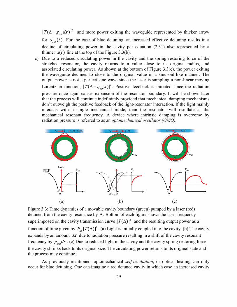
29
2| ( )|omT g dx∆ − and more power exiting the waveguide represented by thicker arrow
for ( )outs t . For the case of blue detuning, an increased effective detuning results in a decline of circulating power in the cavity per equation (2.31) also represented by a thinner ( )a t line at the top of the Figure 3.3(b).
c) Due to a reduced circulating power in the cavity and the spring restoring force of the stretched resonator, the cavity returns to a value close to its original radius, and associated circulating power. As shown at the bottom of Figure 3.3(c), the power exiting the waveguide declines to close to the original value in a sinusoid-like manner. The output power is not a perfect sine wave since the laser is sampling a non-linear moving Lorentzian function, 2| ( )|omT g x∆ − . Positive feedback is initiated since the radiation pressure once again causes expansion of the resonator boundary. It will be shown later that the process will continue indefinitely provided that mechanical damping mechanisms don’t outweigh the positive feedback of the light-resonator interaction. If the light mainly interacts with a single mechanical mode, than the resonator will oscillate at the mechanical resonant frequency. A device where intrinsic damping is overcome by radiation pressure is referred to as an optomechanical oscillator (OMO).
(a) (b) (c)
Figure 3.3: Time dynamics of a movable cavity boundary (green) pumped by a laser (red) detuned from the cavity resonance by ∆ . Bottom of each figure shows the laser frequency superimposed on the cavity transmission curve 2| ( )|T ∆ and the resulting output power as a function of time given by 2| ( )|inP T ∆ . (a) Light is initially coupled into the cavity. (b) The cavity expands by an amount dx due to radiation pressure resulting in a shift of the cavity resonant frequency by omg dx . (c) Due to reduced light in the cavity and the cavity spring restoring force the cavity shrinks back to its original size. The circulating power returns to its original state and the process may continue.
As previously mentioned, optomechanical self-oscillation, or optical heating can only occur for blue detuning. One can imagine a red detuned cavity in which case an increased cavity

30
radius enhances the intracavity power, further pushing the cavity outward. The mechanical spring stiffness may bring the cavity closer to its original size but this will be counteracted by the outward radiation pressure force and intrinsic mechanical damping. For the red detuned case, radiation pressure is in phase with mechanical damping (or friction): When x is decreasing, radiation pressure decreases with it and when x is increasing, radiation pressure is also increasing. The radiation pressure is thus in cohort with the frictional force proportional to m xΓ . Eventually the system will reach a steady state in which the mechanical mode is further damped by radiation pressure, a process known as optical cooling. One can verify that the opposite is true for blue detuning, in which case radiation pressure is out of phase with the mechanical damping force and thus acts as mechanical gain. The frequency domain view of cavity optomechanics in Figure 3.4 is also useful for understanding physically observed phenomena. The laser frequency is now superimposed upon the intracavity photon number 2| ( , )|a t ω plotted vs input frequency similar to Figure 2.3(b). It is assumed that radiation pressure, ( )rpF t interacts with only a single mechanical mode occurring
at angular frequency mΩ . In both red and blue detuned cases, periodic expansion of the radius causes phase modulation of the circulating electric field, and thus phase modulation sidebands positioned at m±Ω from the laser. Observing Figure 3.4(a) when the laser is blue detuned, the lower energy sideband at frequency o mω − Ω is preferentially amplified by the internal cavity response in comparison to the higher frequency sideband. By photon number conservation, the presence of additional low energy photons implies that there is less energy in the electromagnetic field when compared to the stationary cavity case. Energy conservation demands that energy must be flowing from the electromagnetic field to the mechanical resonator. Blue detuning thus leads to amplification of mechanical motion and is amenable to self-oscillation. For red tuning depicted in Figure 3.4(b) the opposite is true as the higher energy sideband is preferred by the cavity response and so photon and energy conservation mandates that energy is funneled from the cavity mechanical degree of freedom to the electromagnetic field. This flow of energy from mechanical to electromagnetic forms, is the basis for optical cooling and the realization of cooling the resonator to the quantum mechanical ground state [7][8].

31
(a) (b)
Figure 3.4: Frequency domain representation of cavity optomechanics. The laser centered at oω
is detuned by ∆ and interacts with a single mechanical mode at mΩ . (a) In the blue detuned case the lower phase modulation sideband preferentially circulates in the cavity while in (b) red detuning amplifies the upper sideband. Mechanical motion is amplified in case (a) and is suppressed for case (b)
Observation of Figure 3.4 shows that exactly on resonance ( 0∆ = ), the optical field can neither cool nor heat the mechanical mode. Though not explicitly drawn, the lower frequency phase modulation sideband at o mω − Ω is actually π phase shifted with respect to the upper sideband and so should be pointing downwards in the figure. When the laser is exactly on resonance, the upper and lower sidebands are equally weighted by the cavity response and thus exactly cancel. No energy may be transferred from laser to the mechanical mode and vice versa, the system behaves as if the cavity position is fixed. If turned on its side, Figure 3.4 may be viewed as a band diagram for photons – the active medium in a phonon laser. In the blue detuned case, upon interaction with a photon, light is more likely to fall from the laser frequency to a lower energy and release a phonon in the process. When blue detuned, the density of photon states is greater for smaller energy photons and the photon field may be viewed as a population inverted in analogy to a traditional laser except here photons replace the role of carriers and phonons replace the role of photons. An astute reader may also realize that the laser samples a non-linear moving optical response and in order to accurately synthesize such a field (which isn’t a perfect sinusoid), multiple harmonics of the phase modulation sidebands are necessary. These internal phase modulation harmonics combine with the field ins within the waveguide to produce amplitude modulation harmonics in the waveguide output field. By measuring the waveguide output field with a high speed photodetector, we observed a frequency comb comprising 40 harmonics in a 74MHz silicon nitride resonator as shown in the figure below. Other groups have studied the relative weight of such harmonics in more detail [10] and the power in each harmonic is derived later in this thesis.

32
0.0 0.5 1.0 1.5 2.0 2.5 3.0
-100
-80
-60
-40
-20
RF P
ower
(dBm
)
Frequency (GHz) Figure 3.5: Optomechanical frequency generated by an 2 74MHzm πΩ = ⋅ , 25μm outer radius SiN optomechanical oscillator pumped with a high optical power of 32mW at the coupling junction. Data was measured at 24Torr with a high speed 10GHz photodetector with integrated transimpedance amplifier.
Optomechanical RF frequency comb generation may also be understood in the time domain in which cavity photons at phase modulation frequency o mω ± Ω may undergo many round trips and thus be re-modulated by the mechanical mode to produce harmonics of frequency
o mNω ± Ω where N is the harmonic number. Optomechanical RF frequency combs permit harmonic locking to a frequency reference demonstrated here for a multimaterial resonator in section 6.2 and by others in [44]. Applications such as chip-scale atomic clocks [13], mass sensing [11], and photonic communications [45] may also benefit from higher order harmonic generation. In section 3.5.1 the optomechanical frequency comb will be analyzed more quantitatively.
3.4 Coupled Mode Equations for Cavity Optomechanics In the previous section, the dynamics of cavity optomechanics were analyzed
qualitatively. Coupled mode theory in section 2.2 for rigid WGM resonators is particularly useful to quantitatively study radiation pressure dynamics in the case of a moving cavity boundary. We continue to adopt the notation and initial formulations in [28].
Substituting equation (3.7) into (2.25) dictates that in the presence of optomechanics, the detuning becomes ( )omg x t∆ → ∆ − . Hence, equations (2.23)-(2.25) describing the dynamics of a rigid resonator are now,
( )( ) ( ) ( ) ( )2om in exa t i g x t a t s tκ κ
= ∆ − − +
(3.18)
( ) ( ) ( )out in exs t s t a t κ= − (3.19)
0o cω ω∆ ≡ − (3.20)

33
where 0cω is the cavity center frequency in the absence of radiation pressure. Treating the mechanical mode, parameterized by scalar position ( )x t , as a damped harmonic oscillator driven by rpF completes the system of equations,
( )2 2( ) ( ) ( ) ( ) .ex om eff m mF g a t m t t tx x x− = + Γ + Ω (3.21)
In writing (3.21), an arbitrary external driving force, exF is included along with radiation pressure from equation (3.10). The general relation between mechanical stiffness, K , resonant frequency, mΩ and effective mass, effm also applies,
meff
Km
Ω = (3.22)
Equation (3.21) implies that the mechanical effective mass may be understood as the moving mass in the direction of ( )x t such that the maximum energy stored in the mechanical mode is,
2 2max
1 | |2m eff mU m x= Ω (3.23)
which is the usual energy stored in a one dimensional harmonic oscillator. However, recall from section 3.2.1 that the definition of x is arbitrary for three dimensional structures and thus, so is
effm . If x is scaled by α , effm must be scaled by 2α − to maintain the non-arbitrary mode energy of equation (3.23). Here, ( )x t is defined as the radial movement of the point along the boundary with largest radial displacement. Since each mechanical mode experiences a different maximum displacement, each mechanical mode also has a different effective mass and optomechanical coupling. An important figure of merit for the mechanical resonator is the intrinsic mechanical quality factor,
mm
m
QΩ
=Γ
(3.24)
which is derived analogous to equation (2.14). Replacing κ in equation (2.14) is mΓ , the intrinsic mechanical damping rate and FWHM of the mechanical mode in angular frequency space. In our measurements, mQ is determined from the FWHM of the mechanical displacement peak which is always driven by thermal Brownian motion at room temperature. i.e. the thermal force acts as a pervasive white driving source in the broadband measurement technique of section 2.3 As a first step, the coupled equations (3.18) and (3.21) are solved numerically using a standard differential equation solver. In Figure 3.6(a) the displacement is solved for in time for four different optical input powers using the stiffness switching method in Mathematica. A blue detuned PSG cavity was assumed for each case. In all cases, the displacement varies

34
harmonically at a frequency of / 2m πΩ = 18.3MHz and the displacement amplitude increases from 30fm to 3pm when the power is increased from 470μW to 47mW. In this regime, the displacement amplitude is linear with input power. The output power shown in Figure 3.6(b) however behaves differently. In all three cases, it begins at the input power ( / 1out inP P = ), and then drops as the cavity charges to optical steady state. The output power then momentarily increases as the displacement momentarily increases to its steady state value, x . Once the displacement reaches steady state, the output power then behaves very differently depending on the input power. Evident in the plots is that somewhere between an input power of 2.4mW and 9.4mW, the output power oscillates sinusoidally at the same frequency as the displacement, a signature of self-oscillation which was detailed qualitatively in the context of Figure 3.3. In section 3.6.1 the threshold power for self-oscillation will be analytically determined and trends with relevant figure of merits will be investigated.
0
10
20
30
0 1 2 3 4 5
0
50
100
150
0
200
400
600
0 1 2 3 4 5
0
1000
2000
3000
Pin=470µW
Pin=2.4mW
Disp
lace
men
t (fm
)
Pin=9.4mW
Pin=47mW
Time (Ωm/2π)-1
0.36
0.38
0.40
0.42
0 1 2 3 4 5
0.36
0.38
0.40
0.42
0.36
0.38
0.40
0.42
0 1 2 3 4 50.36
0.38
0.40
0.42
Pin=470µW
Pin=2.4mW
Pin=9.4mW
Pout
/Pin
Pin=47mW
Time (Ωm/2π)-1
(a) (b)
Figure 3.6: a) Displacement and b) corresponding output power vs time for four different input powers. A blue detuned cavity with intrinsic optical Q of 1 million, mechanical Q of 1160,
112.4 10 kgeffm −= × , R=52.5μm, /om cg Rω= − = -23GHz/nm was assumed. The detuning and
loaded optical Q were / oκ∆ = 0.3 and 750k respectively.
3.5 Large Signal Dynamics It was demonstrated in section 3.3 that in principle, a blue detuned laser may excite a
mechanical mode into self-oscillation and that the output field may comprise an RF frequency

35
comb with optical carrier. One option to predict and study these dynamics is to solve equations (3.18)-(3.21) with a numerical differential equation solver such as Matlab or Mathematica as was performed in the previous section. However, numerical solutions are often slow and a more analytical solution is sought. As a first step, the equations may be simplified by assuming the displacement is sinusoidal thus replacing equation (3.21) with the relation,
( ) sin( ).o mx t x x t= + Ω (3.25)
It was assumed in (3.25) that the displacement oscillates about some steady state value, x with a magnitude of ox as was observed in Figure 3.6(a). Switching to a fixed frame not rotating at the laser frequency makes the time dynamics more physical. Substituting (3.25) into (3.7), equation (2.21) becomes,
( )( ) sin( ) ( ) ( )e .2
oi tc om om o m in exa t i g x g x t a t s t ωκω κ−
= − + + Ω − +
(3.26)
From the supplementary section of [46] the homogenous, ( )ha t and particular, ( ) ( ) ( )p ha t A t a t= solutions of the differential equation above satisfy,
0( ) exp ( ) cos( )2h c om ma t A i g x t i tκω β
= − + − − Ω
(3.27)
( )( ) exp cos( )2in ex c om m oA t s i g x t i t i tκκ ω β ω
= + + + Ω −
(3.28)
where 0A depends on the initial cavity condition. The modulation index,
oom
m
xgβ ≡ −
Ω (3.29)
was also introduced. In contrast to [46], input field of the form oi tins e ω− was assumed rather than
oi tins e ω+ resulting in i i→ − in the equation solutions. In the end, the convention doesn’t matter
since computation of physically measured photocurrent eliminates the oi te ω± dependence. Substitution of the common expansion,
cos( ) ( )m mi t in tnnn
e i J eβ β+∞Ω − Ω
=−∞= ∑ (3.30)
where ( )nJ β are Bessel function of the first kind, allows integration of (3.28) yielding,
( ) cos( )0 ( )( )
/ 2 ( )o m m
ni n t i tn
p in exn om m
i Ja t A s e
i g x nω ββ
κκ
+∞− + Ω − Ω
=−∞
=− ∆ − + Ω∑ (3.31)

36
Due to the / 2κ dependence in ( )ha t the general solution ( ) ( ) ( )h pa t a t a t= + quickly
converges to ( )pa t . We can then expand the cos( )mi te β− Ω in (3.31) utilizing the Bessel expansion of (3.30) yet again to write ( )a t after 2/κ seconds,
( )0
,
( ) ( )( ) ( ) .
/ 2 ( )o m
n mi n m tn m
p in exn m m
i J Ja t a t A s e
i nωβ β
κκ
−+∞ − + − Ω
=−∞
= =− ∆ + Ω∑ (3.32)
In writing, (3.32), the relation, ( )m mi i −− = was used and the effective detuning,
omg x∆ ≡ ∆ − (3.33)
was introduced. Throughout this section we assume the initial condition that at 0t = , we have (0) (0) (0) | | i
p ha a a a e β−= + = where a is the steady state cavity mode amplitude similar to
(2.26) with ∆ → ∆ . Substituting 0t = into equations (3.27) and (3.31) then gives,
( )
0
2
( )i
| |
1 | |n
nin ex
nmi
J
aA
snκ
βκ
∞
=−∞ −
=
+∆ + Ω
∑
(3.34)
It was assumed that the phase of ins was chosen so that when multiplied by the entire summation
the product is real allowing for the absolute value of the product. For low Q cavities, 0 ~ 1A but for high Q cavities it varies strongly with β . For brevity, 0A is dropped in the following equations but is kept in all calculations.
3.5.1 Frequency Comb Generation Observation of (3.32) shows that the field in the cavity consists of a comb of sidebands at
frequencies ( ) mn m− Ω offset from the optical carrier at oω . Since n m− is either an integer or
zero, the comb lines extend out from oω and occur at integer multiples of mΩ in both the positive and negative frequency directions. This frequency comb is usually detected at the output of the waveguide with a photodetector sensitive to the output optical power,
2
( ) .out o outP s tω= (3.35)
Using (2.22) and assuming CW input field we find,
( ) e ( )oi tout in exs t s a tω κ−= − (3.36)
37
2 2 2* *
2 2*
( ) ( ) ( ) ( )
2Re ( ) ( )
o o
o
i t i tout in ex in ex in ex
i tin ex in ex
s t s a t s e a t s e a t
s a t s e a t
ω ω
ω
κ κ κ
κ κ
−= − − +
= − +
(3.37)
consistent with reference [46] with i i→ − as previously mentioned.
3.5.2 Output Power in the hth Harmonic Applications utilizing an optomechanical frequency comb may require high RF power at
the harmonic of interest. It is thus interesting to derive the optical power at a particular harmonic. Though it is suspected that such a derivation has been performed elsewhere, it hasn’t been found in the literature. In [10] an approximate solution for harmonic power was derived that approximates the optical cavity Lorentzian as a linear function for small oscillation amplitude. In [9], the authors elude to calculating the harmonic strength by Taylor expansion of equation (3.18) but no derivation was given. Since the oscillation amplitude may be large for high finesse cavities or for large pumping power, the following derivation is more general as it only assumes sinusoid displacement equation (3.25) and is valid even in the large amplitude regime. Such a derivation is also useful in understanding how the optomechanical oscillator converts RF power from one harmonic to the next. The derivation is even valid for converting DC power up to higher frequencies through internal frequency mixing. The time varying terms in (3.37) are analyzed separately. From (3.32), the first term varying as a function of time in (3.37) may be written,
( )
( )
* 2
( )2 2,
( )2
,
2Re ( ) 2| | Re
( ) ( ) / 2 ( )
/ 2 ( )
2| | Re ( )
o
m
m
i tex in in ex
n mn m m i n m t
n mm
i n m tn min ex n m
n m
a t s e s
i J J i ne
n
s A J i e
ωκ κ
β β κ
κ
κ β
−+∞− − Ω
=−∞
+∞− − Ω−
=−∞
− = −+ ∆ + Ω + ∆ + Ω
= −
∑
∑
(3.38)
Where nA is defined as,
( )
( )2 2
( ) / 2 ( ).
/ 2 ( )n m
n
m
J i nA
n
β κ
κ
+ ∆ + Ω≡
+ ∆ + Ω (3.39)
The output optical power oscillating as mih te − Ω is found by choosing only summation terms which satisfy,
n m h− = ± (3.40)
where not to be confused with planks constant, in this context h is an integer for the thh harmonic. Keeping only these relevant terms eliminates the summation over m ,

38
* 2
2 *
2Re ( ) 2| | Re ( ) ( )
2| | Re ( ) ( )
o m mi t ih t ih th hex in in ex n n h n n h
n
in ex n n h h n n h hn
a t s e s A J i e A J i e
s A J B A J B
ωκ κ β β
κ β β
+∞− Ω Ω−
− +=−∞
+∞
− +=−∞
− = − +
= +
∑
∑ (3.41)
with the definition,
.mih thhB i e − Ω≡ (3.42)
Now, using the general relation, *Rea ( )/ 2a a= + gives,
( ) ( )
* 2 * * * *
2 * * * *
2 *
2Re ( ) | |
| |
2| | Re Re
oi tex in in ex n n h h n n h h n n h h n n h h
n
in ex n h n h n h n h n h n hn
in ex n h n h n h n hn
a t s e s A J B A J B A J B A J B
s J A B A B J A B A B
s J A B J A B
ωκ κ
κ
κ
+∞
− + − +=−∞
+∞
− +=−∞
+∞
− +=−∞
− = − + + +
= − + + +
= − +
∑
∑
∑
(3.43)
For now, the argument, β from the Bessel functions was dropped for brevity. To find the real
part of each argument, first the handy relation 2i
i eπ
= is used to rewrite (3.42),
22 2m
m m
hih ti ihih t ih t
hB e e e e eππ π
− Ω − − Ω − Ω
= = =
. (3.44)
We find using (3.39),
( )
( )
2 2
*2 2
( ) cos ( )sin2 2 2
Re/ 2 ( )
( ) cos ( )sin2 2 2
Re/ 2 ( )
n m m m
n h
m
n m m m
n h
m
J h t n h tA B
n
J h t n h tA B
n
κ π πβ
κ
κ π πβ
κ
Ω − + ∆ + Ω Ω −
=+ ∆ + Ω
Ω − − ∆ + Ω Ω −
=+ ∆ + Ω
Substitution into (3.43) finally gives,

39
( )
( )
( )
* 22 2
cos sin, ,
cos
( )2Re ( ) 2| |
/ 2 ( )
cos2 2
( ) sin2
cos( ) sin( )2 2
cos(
oi t nex in in ex
nm
n h n h m
m n h n h m
n h m n h mn
h
Ja t s e s
n
J J h t h
n J J h t h
C h t h C h t h
C h
ω βκ κ
κ
κ π
π
π π
+∞
=−∞
− +
− +
+∞
+ +=−∞
+
− = − × + ∆ + Ω
+ Ω − +
∆ + Ω − Ω −
= Ω − + Ω −
= Ω
∑
∑
sin) sin( )2 2m h mt h C h t hπ π
+− + Ω −
(3.45)
Where the cosine and sine coefficients, cosC and sinC were inserted and have obvious definitions from (3.45). Though it may seem like many terms contribute to the power at the thh harmonic, the contribution to the sum rapidly decreases as | | / 2mn κ∆ + Ω > . If the system is blue detuned ( 0)∆ > , then only terms satisfying
/ 2 ( 0)
( / 2 ) ( 0)
m
m
n for n
n for n
κ
κ
− ∆< >
Ω
− + ∆> <
Ω
(3.46)
need to be included in the sum over n . Physically, the thn term represents the power that the thn harmonic contributes back to the thh harmonic after photon recycling and internal mixing within the cavity produces a cascade of sidebands from frequency mnΩ to mhΩ . When the conditions of (3.46) are not met, the sideband is suppressed by the cavity Lorentzian response. We now turn to the 2nd time varying term in (3.37), ( )a*(t)ex a tκ . It is easiest to begin
with the form of ( )a t in equation (3.31) and use the relation 2 *
,n n mn n ma a a=∑ ∑ along with
(3.33) to find,
( )
( )( )( )
( )
2 2 2
,
2 2
,
( ) ( )( ) | |
/ 2 ( ) / 2 ( )
( )| |
/ 2 ( )
m
m
i n m tn mn m
ex in exn m m m
i n m tn mm
in ex nn m m
i J J ea t s
i n i m
i J es A
i m
β βκ κ
κ κ
βκ
κ
− − Ω−+∞
=−∞
− − Ω−+∞
=−∞
⋅=
− ∆ + Ω + ∆ + Ω
⋅=
+ ∆ + Ω
∑
∑
(3.47)

40
The coefficient, nA has the same definition as (3.39). Once again, only terms satisfying (3.40) contribute to the thh harmonic and keeping these terms gives,
2 *2
2 2 *
( ) ( )( )
( ( ) ) ( ( ) )2 2
| |
1 2
in ex n n h h n n h hex
nom m
in ex n n h h n n h hn
n
P A J B A J Ba t
i n h i n h
s A D B A D B
Term Term
κ β βκ
ω κ κ
κ
+∞− +
=−∞
+∞
− +=−∞
+∞
=−∞
= +
+ ∆ + − Ω + ∆ + + Ω
= +
= +
∑
∑
∑
(3.48)
where hB retains the same definition of (3.42) and the new coefficients are,
( )
( )
22
22
( ) ( ( ) )( ) 2
( ( ) ) ( )2 2
( ) ( ( ) )( ) 2
( ( ) ) ( )2 2
n h mn h
n h
m m
n h mn h
n h
m m
J i n hJ
Di n h n h
J i n hJ
Di n h n h
κββ
κ κ
κββ
κ κ
−−
−
++
+
− ∆ + − Ω
≡ = + ∆ + − Ω + ∆ + − Ω
− ∆ + + Ω
≡ = + ∆ + + Ω + ∆ + + Ω
(3.49)
Now, equation (3.48) would simplify nicely if ( )*n n h n n hA D A D− −= but this is not the case. However, investigation of the definition for nA in equation (3.39) and comparison to (3.49) reveals fortuitous circumstances:
( )
( )
n n h n h n
n n h n h n
A D A D
A D A D
∗
− −
∗
+ +
=
= (3.50)
The above relations are motivated by knowledge that 2| ( )|ex a tκ is real and we then seek coefficient pairs which are the complex conjugates of each other. Equation (3.50) shows that
1Term in (3.48) is added to its complex conjugate when n n h→ − in 2Term . Likewise, 2Term eventually is added to its conjugate, 1Term when n n h→ + . i.e.
41
1 2( )2 1( )
Term Term n n hTerm Term n n h
∗
∗
= → −
= → +
By pre-emptively adding the complex conjugate partner to each term within the summation, the summation argument of (3.48) is reduced to sines and cosines,
( )
2
2 2 *
2 2 *
( ) 1 2
1 1 2( ) 2 1( )2
Re 1 Re 2
Re 1 2
| | Re
| | Re
exn
n
n
n
in ex n n h h n n h hn
in ex n n h h n h hn
a t Term Term
Term Term n n h Term Term n n h
Term Term
Term Term
s A D B A D B
s A D B D B
κ
κ
κ
+∞
=−∞
+∞
=−∞
+∞
=−∞
+∞
=−∞
+∞
− +=−∞
+∞
− +=−∞
= +
= + → − + + → +
= +
= +
= +
= +
∑
∑
∑
∑
∑
∑
(3.51)
Inserting the definitions, (3.39), (3.44), (3.49) and after some algebra,
( ) ( )
( )( )
2 2 22 22 2
2
( ) | |/ 2 ( ) / 2 ( ( ) )
( ) cos( )2 2
sin( ) ...( ) ( )...2 2
n n hex in ex
nm m
m m m
mm
J Ja t s
n n h
n h n h t h
hh t h n h n h
κ κκ κ
κ π
κ π
+∞−
=−∞
= + ∆ + Ω + ∆ + − Ω + ∆ + − Ω ∆ + Ω Ω −
Ω + Ω − + − → +
∑
where ( ) ( )n h n h− → + implies that everything in the square brackets is repeated except when ( )n h− appears it is replaced by ( )n h+ . The expression above is simplified somewhat by substitution of the relations,
( )( ) ( ) ( )( )( ) ( ) ( )
2
2
( ) ( ) ( )
( ) ( ) ( )m m m m m
m m m m m
n h n n h h n h
n h n n h h n h
∆ + − Ω ∆ + Ω = ∆ + − Ω + Ω ∆ + − Ω
∆ + + Ω ∆ + Ω = ∆ + + Ω − Ω ∆ + + Ω
to finally obtain,

42
( )
( ) ( )
( ) ( )
2 22 2
2 22
2 2 22 2
2
( ( ) ) ( ( ) )cos( )
2/ 2 ( ( ) ) / 2 ( ( ) )
( ) ( )
/ 2 ( ( ) ) / 2 (
( )( ) | |
/ 2 ( )
m
m m n h m m n hn h n h m
m m
n h n h
m
nex in ex
nm
h
h n h J h n h JJ J h t h
n h n h
J J
n h
Ja t s
n
κ
π
κ κ
β β
κ κ
βκ κ
κ
− +
− +
− +
+∞
=−∞
Ω
Ω ∆ + − Ω Ω ∆ + + Ω+ + − Ω −
+ ∆ + − Ω + ∆ + − Ω
++ ∆ + − Ω + ∆
= + ∆ + Ω
+
∑
2
cos sin, ,h
cos sin
sin( )2( ) )
cos( ) sin( )2 2
cos( ) sin( )2 2
m
m
n h m n mn
h m h m
h t hn h
C h t h C h t h
C h t h C h t h
π
π π
π π
+∞
− −=−∞
− −
Ω −+ + Ω
= Ω − + Ω −
= Ω − + Ω −
∑
(3.52)
The reader is reminded that modulation index argument of the Bessel functions defined by equation (3.29), was omitted in some instances for compactness. Since, the modulation index depends linearly on the displacement amplitude, ox , which is numerically determined through (3.21), many of the resonator mechanical properties are buried within the Bessel function arguments.
The output optical power oscillating at RF angular frequency, mh tΩ is the sum of (3.45) and (3.52):
( ) ( ), , , ,
sin, ,
sin
cos( ) sin( )2 2
cos( ) sin( )2 2
(@ )
cos( ) sin( )2 2
cos cos sin sinn h n h m n h n h m
cosn h m n h m
out m on
on
coso h m h m
C C h t h C C h t h
C h t h C h t h
P h t
A h t h A h t h
π π
π π
ω
ω
π πω
+ − + −
∞
=−∞
∞
=−∞
+ Ω − + + Ω −
Ω − + Ω −
Ω =
=
= Ω − + Ω −
∑
∑
(3.53)
where the coefficients, hA are the sum of all the ,n hC coefficients. Also, for blue detuning, only the terms in (3.46) need to be kept in each sum. High optical Q cavities thus always have fewer terms contributing to the sum. The sine and cosine components of the output power at harmonic h add in quadrature. Since the phase of each quadrature contains / 2hπ− in the argument, the “in-phase” and “quadrature” components depend on the harmonic in question.
Often, the frequency comb is monitored on a an electrical spectrum analyzer (ESA) which responds to the envelope of the incoming photodetected power [47],
( ) ( )2 2cos sin, ( )env opt m o h hP @h t A AωΩ = + . (3.54)

43
Equation (3.54) is the optical power in the thh harmonic exiting the device. Upon photodetection, the measured RF power is proportional to the RF voltage squared and thus (3.54) is used to find the RF power viewed on an ESA at frequency mh tΩ ,
( ) ( ) ( )2 22 cos sin
2
, (@ )RF o v o h h
envsig rf m
load load
G R T A AVP h
R R
ω + Ω = =
(3.55)
where vR is the voltage responsivity [volts/watt] of the photodetector, loadR is the input
resistance of the ESA, RFG is the RF gain between the photodetector and ESA, and oT is the optical transmission between the coupling junction and photodetector.
3.5.3 Carrier Power The amount of power in the first harmonic ( 1h = ), or “fundamental” is defined as the
carrier power. In any oscillator it is imperative to have large carrier power with little degradation in noise for improved signal to noise ratio and performance. To find the carrier power, first 1h = is substituted into equations (3.45) and (3.52) to plot the coefficients cos cos sin, , ,h h hC C C+ − + and sin
hC − as a function of displacement amplitude, ox . Figure 3.7 shows an example of such a calculation for our typical spoked-ring PSG OMO device at atmosphere. The chosen device has a 52.5μm radius
2 18.3m MHzπΩ = ⋅ , mQ = 1170, 112.4 10effm kg−= × , and /o cg Rω= − at 1550nm. The coefficients are plotted for four values of intrinsic optical Q as shown in Figure 3.7. Intrinsic
'Q s ranging from a lower oQ of 100,000 to a rather high oQ of 100 million attained in laser-
reflowed microtorroids [38] are chosen. The effective detuning, ∆ , and loaded optical Q , totQ specified in each graph, are chosen to minimize the threshold power for self-oscillation - an optimization which will be detailed in section 3.6.1.

44
-0.10.00.10.20.3
10-13 10-12 10-11 10-10 10-9 10-8
0.00.10.20.3
-0.20.00.20.40.6
10-13 10-12 10-11 10-10 10-9 10-8-0.8-0.40.00.40.8
Qo=100k, Qtot=75k∆/κo=0.3
Qo=1M, Qtot=750k∆/κo=0.3
Ccosh+
Ccosh-
Csinh+
Csinh-
Coef
ficie
nts f
or P
out(@
Ωm)/P
in
Qo=10M, Qtot=5.9M∆/κo=0.7
Qo=100M, Qtot=16M∆/κo=8
Displacement Amplitude, xo (m) Figure 3.7: Coefficients to calculate carrier power plotted vs displacement amplitude, ox . The
coefficients are each normalized by dividing by 2| | /in in os P ω= .
In studying Figure 3.7 several trends are evident:. 1) The sinhC ± coefficients which multiply
sin( / 2)mh t hπΩ − are negligible for low oQ devices, but become very significant for high oQ . We will see in section 3.6.1 that once the intrinsic linewidth is less than the mechanical frequency, the sideband resolved regime is attained which gives new dynamics such as higher component of optical power oscillating as sin( / 2)mh t hπΩ − . For 1h = , sin( / 2) cos( )m mh t h h tπΩ − = − Ω so in comparing to (3.25) this represents the quadrature component of the oscillating field. 2) High oQ devices have larger coefficients at small displacements, and the separate sums of the cosine and sine coefficients has a greater maximum when compared to low oQ devices. This is evident by the scales of the four plots above. This
shouldn’t be too surprising since a high oQ device has a larger Lorentzian slope in frequency and so will modulate the stored laser field more for a given displacement. Note that the input optical power required to reach a given displacement has not been mentioned but it should be evident from previous discussions that high oQ gives larger displacement amplitude for a given input power. However, a consequence of the greater input power to radiation pressure force is that the carrier power of high oQ will saturate at low input power since Figure 3.7 shows that 3) after a
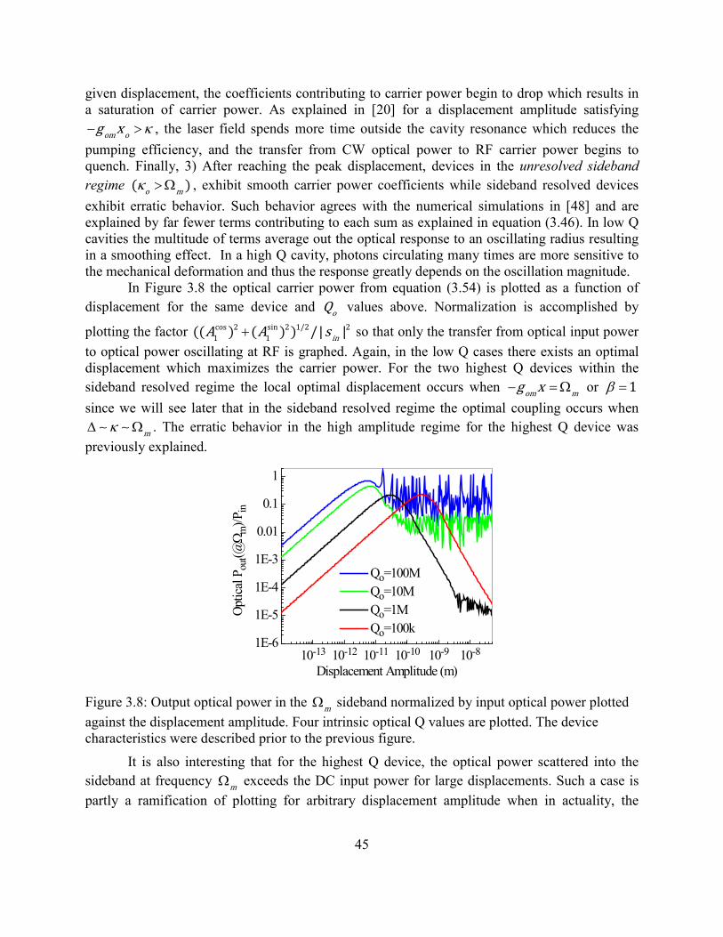
45
given displacement, the coefficients contributing to carrier power begin to drop which results in a saturation of carrier power. As explained in [20] for a displacement amplitude satisfying
om og x κ− > , the laser field spends more time outside the cavity resonance which reduces the pumping efficiency, and the transfer from CW optical power to RF carrier power begins to quench. Finally, 3) After reaching the peak displacement, devices in the unresolved sideband regime ( )o mκ > Ω , exhibit smooth carrier power coefficients while sideband resolved devices exhibit erratic behavior. Such behavior agrees with the numerical simulations in [48] and are explained by far fewer terms contributing to each sum as explained in equation (3.46). In low Q cavities the multitude of terms average out the optical response to an oscillating radius resulting in a smoothing effect. In a high Q cavity, photons circulating many times are more sensitive to the mechanical deformation and thus the response greatly depends on the oscillation magnitude. In Figure 3.8 the optical carrier power from equation (3.54) is plotted as a function of displacement for the same device and oQ values above. Normalization is accomplished by
plotting the factor cos 2 sin 2 1/2 21 1(( ) ( ) ) /| |inA A s+ so that only the transfer from optical input power
to optical power oscillating at RF is graphed. Again, in the low Q cases there exists an optimal displacement which maximizes the carrier power. For the two highest Q devices within the sideband resolved regime the local optimal displacement occurs when om mg x− = Ω or 1β = since we will see later that in the sideband resolved regime the optimal coupling occurs when
mκ∆ Ω . The erratic behavior in the high amplitude regime for the highest Q device was previously explained.
10-13 10-12 10-11 10-10 10-9 10-81E-6
1E-5
1E-4
1E-3
0.01
0.1
1
Qo=100M Qo=10M Qo=1M Qo=100k
Optic
al P o
ut(@
Ωm
)/Pin
Displacement Amplitude (m) Figure 3.8: Output optical power in the mΩ sideband normalized by input optical power plotted against the displacement amplitude. Four intrinsic optical Q values are plotted. The device characteristics were described prior to the previous figure.
It is also interesting that for the highest Q device, the optical power scattered into the sideband at frequency mΩ exceeds the DC input power for large displacements. Such a case is partly a ramification of plotting for arbitrary displacement amplitude when in actuality, the

46
displacement amplitude begins to saturate upon reaching the value defined by omg x κ− = due to inefficient pumping of the cavity [20]. However, in [48] it was shown that indeed the quantum efficiency for scattering photons into the first sideband may exceed unity for large displacement amplitudes and high Q cavities in the deeply sideband resolved regime. This is due to multiphoton emission as photons inside a cavity with large optical lifetime may make many round trips and contribute to several phonon creation events in the process. The quantum efficiency for such a process may actually greatly exceed one for cavities with large optomechanical coupling and high optical Q’s.
Now, the amount of input power necessary to achieve a given displacement amplitude has not yet been mentioned. The displacement amplitude may be determined numerically for the given input power as was performed to generate Figure 3.6. From the amplitude, the normalized optical carrier power, cos 2 sin 1/2 2(( ) ( ) )/| |h h inA A s+ may then be calculated. In Figure 3.9 both the displacement (a) and corresponding optical carrier power (b) are plotted for the same intrinsic optical Q values previously described. To calculate the displacement, equations (3.18) and (3.21) were numerically integrated using the stiffness switching method in Mathematica. Once the displacement as a function of time was found, it was fitted to a sine wave. Since, the fitted displacement magnitude, ox has a somewhat erratic dependence on input power, the RMS displacement is plotted as suggested in [48]. Once the RMS displacement is known, the normalized optical carrier power may be calculated using equations (3.54) and (3.53) with 1h =
and 2o RMSx x= .
10-6 10-5 10-4 10-3 10-2 10-1 100 101 102 103
10-15
10-14
10-13
10-12
10-11
10-10
10-9
Qo=100M Qo=10M Qo=1M Qo=100k
Disp
lacem
ent (
m)
Input Power (W)10-6 10-5 10-4 10-3 10-2 10-1 100 101 102 103
10-3
10-2
10-1
100
Qo=100M Qo=10M Qo=1M Qo=100k
Optic
al Ca
rrier
Pow
er /
Inpu
t CW
Pow
er
Input Power (W) Figure 3.9: (a) Calculated RMS displacement vs CW optical power present at the waveguide-device coupling junction. Equations (3.18) and (3.21) were numerically evaluated for the four listed intrinsic optical Q values with totQ and ∆ as listed in Figure 3.7. (b) Normalized optical carrier power for the corresponding displacements and input power from part a).
In viewing Figure 3.9a) a knee in the displacement curve reduces the slope at the point /ox κ= − ∆ which is clearly visible in the two highest Qo devices, but the transition is smoother
in the two lower Qo cases (they have a more gradual cavity Lorentzian). This is again due to a high photon sensitivity to a cavity frequency shift beyond the cavity linewidth which decreases
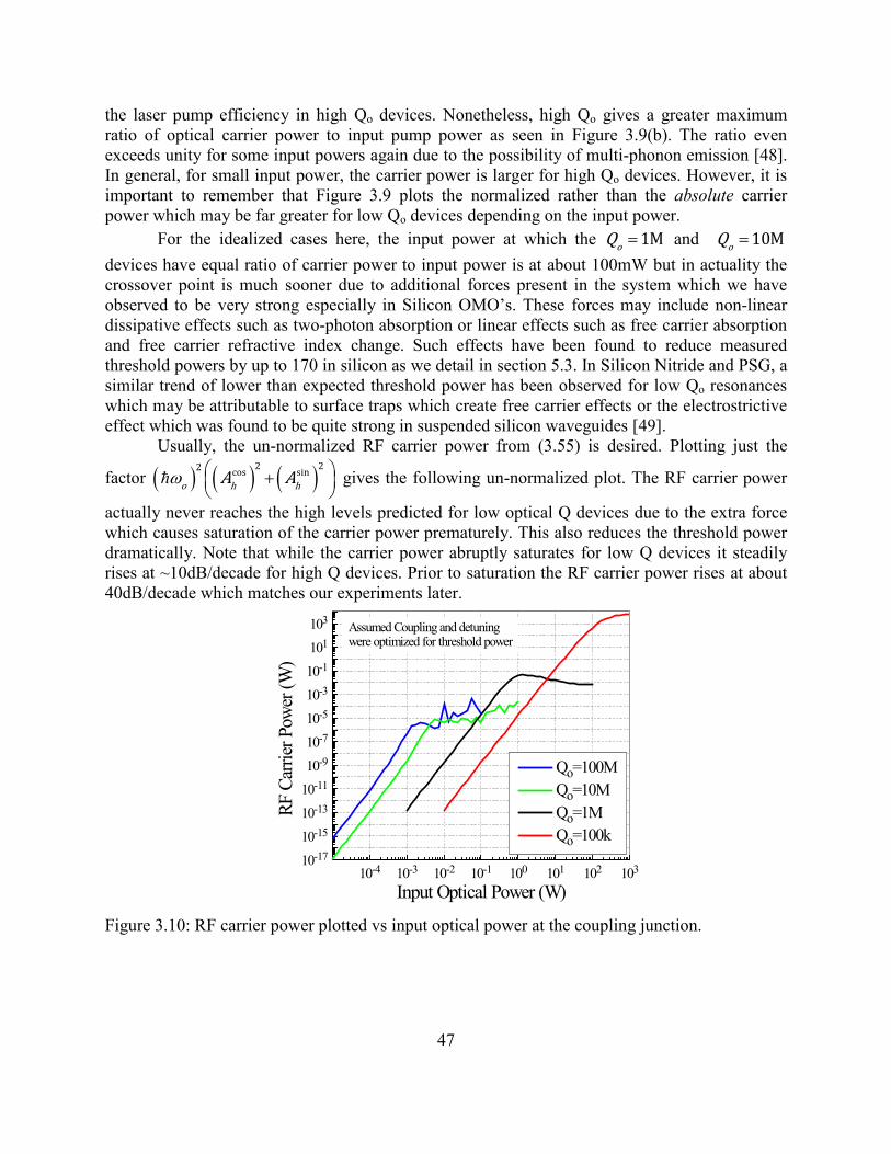
47
the laser pump efficiency in high Qo devices. Nonetheless, high Qo gives a greater maximum ratio of optical carrier power to input pump power as seen in Figure 3.9(b). The ratio even exceeds unity for some input powers again due to the possibility of multi-phonon emission [48]. In general, for small input power, the carrier power is larger for high Qo devices. However, it is important to remember that Figure 3.9 plots the normalized rather than the absolute carrier power which may be far greater for low Qo devices depending on the input power.
For the idealized cases here, the input power at which the 1MoQ = and 10MoQ = devices have equal ratio of carrier power to input power is at about 100mW but in actuality the crossover point is much sooner due to additional forces present in the system which we have observed to be very strong especially in Silicon OMO’s. These forces may include non-linear dissipative effects such as two-photon absorption or linear effects such as free carrier absorption and free carrier refractive index change. Such effects have been found to reduce measured threshold powers by up to 170 in silicon as we detail in section 5.3. In Silicon Nitride and PSG, a similar trend of lower than expected threshold power has been observed for low Qo resonances which may be attributable to surface traps which create free carrier effects or the electrostrictive effect which was found to be quite strong in suspended silicon waveguides [49].
Usually, the un-normalized RF carrier power from (3.55) is desired. Plotting just the
factor ( ) ( ) ( )2 22 cos sino h hA Aω +
gives the following un-normalized plot. The RF carrier power
actually never reaches the high levels predicted for low optical Q devices due to the extra force which causes saturation of the carrier power prematurely. This also reduces the threshold power dramatically. Note that while the carrier power abruptly saturates for low Q devices it steadily rises at ~10dB/decade for high Q devices. Prior to saturation the RF carrier power rises at about 40dB/decade which matches our experiments later.
10-4 10-3 10-2 10-1 100 101 102 10310-1710-1510-1310-1110-910-710-510-310-1101103
Qo=100M Qo=10M Qo=1M Qo=100k
RF C
arrie
r Pow
er (W
)
Input Optical Power (W)
Assumed Coupling and detuningwere optimized for threshold power
Figure 3.10: RF carrier power plotted vs input optical power at the coupling junction.

48
3.6 Small Signal Dynamics Thus far it has been assumed the device radius oscillates harmonically without regards to
the input power necessary to achieve such a state. Per section 3.3, when the input light is blue detuned with respect to the cavity resonance, the force due to radiation pressure is out of phase with the mechanical frictional damping and self-oscillation is possible. In other words, radiation pressure exerts mechanical gain on the structure. This gain is due to the dynamical nature of radiation pressure. For blue detuning, the radiation pressure is reduced as the device expands, and vice versa for red detuning. The light and mechanical structure act as a dynamical system as each are affected by the dynamics of the other. The interplay of the time varying and interdependent optical and mechanical states is referred to as dynamical back-action. In this section, the previously introduced optomechanical coupled mode equations will be evaluated in the small signal limit to derive the damping (or gain) due to dynamical back action. From the optomechanical damping, the threshold power will be calculated and its behavior evaluated in certain regimes.
Also, in the previous section, the sideband power oscillating at integer multiples of the mechanical frequency was calculated and it was assumed the resulting spectrum was a train of perfect delta functions with peak height given by the sideband power. In reality, noise perturbs the instantaneous mechanical frequency resulting in a broadening of each peak in the optomechanical frequency comb. Any oscillator should have large signal to noise ratio while consuming minimal power. The carrier power, or signal, has already been derived and analysis of the noise and minimum input power for oscillation is forthcoming.
Steady State Solutions
First, steady state solutions to the optomechanical coupled mode equations, (3.18)- (3.21) are sought. Substituting ( )a t a→ , ( )x t x→ , ( )in ins t s→ gives,
2 2
0 ( )2
| |
om in ex
ex om eff m
i g x a s
F g a m x
κ κ
= ∆ − − +
− = Ω
(3.56)
Re-arranging gives,
2
2
( ) / 2
| |.
exin
om
ex om
eff m
a si g x
F g ax
m
κκ
=− ∆ − +
−=
Ω
(3.57)
The non-linear interdependence of a and x above gives rise to a well-known bistability and hysteresis when sweeping a laser through an optomechanical cavity in the absence of an external force, extF [50].

49
Small Signal Solutions The coupled optomechanical equations are linearized by assuming a small signal limit.
All dynamical variables, are written as a sum of a static steady state (or average) value and a time varying (or small signal) component,
( ) ( )( ) ( )( ) ( )( ) ( )
in in in
out out out
a t a a tx t x x t
s t s s ts t s s t
δδδδ
= += += += +
(3.58)
In the small signal limit, it is assumed that ( )a t aδ holds for all variables. While this assumption is perfectly valid for analyzing gain just prior to self-oscillation, and noise components which depend linearly on the dynamical variables, it would be invalid to apply the same assumption to harmonically oscillating variables during self-oscillation which may approach their steady state counterpart. Equations (3.58) are then substituted into (3.18) and (3.21) to obtain,
( ) ( ) ( )
( )( )( )
2 * 2
2
( ) ( ) ( ) ( )
( ) | | ( ) ( ) | ( )|
( ) ( ) ( )
om in in ex
ex ex om
eff m m
t i g x t a + a t s + s t k2
F F t g a a a t a a t a tm t t x x t
a
x x
κδ δ δ δ
δ δ δ δ
δ δ δ
∗
= ∆ − − +
+ − + + +
= + Γ + Ω +
(3.59)
where (3.33) was substituted for the steady state detuning omg x∆ ≡ ∆ − . Next, equation (3.56) is substituted above to remove some of the steady state terms, then small signal products to second order such as 2| |aδ and a xδ δ⋅ are ignored, followed by assuming the phase of ins is adjusted to make a real. Performing these operations leads to the linearized equations,
( ) ( )2
( ) ( ) ( ) ( )
( ) ( ) ( ) ( ) ( ) ( )
om in ex
ex om eff m m
t i a t ig a x t s t k2
F t g a a t a t m t t t
a
x x x
κδ δ δ δ
δ δ δ δ δ δ∗
= ∆ − − +
− + = + Γ + Ω
Performing a Fourier transform of the form x( ) ( ) i tt x t e dtΩ= ∫ on both equations renders
them algebraically solvable. Recall that Fourier theory demands ( ) ( ) i tx t x e d− Ω= Ω Ω∫ so that
( ) ( )t ix x Ω= − Ω⋅ and 2( ) ( )tx x Ω= −Ω . The property, ( ) ( )x t x∗ ∗Ω= − also
holds. Integrating the time dependent coupled mode equations then gives the frequency domain equivalent,

50
( ) 1
( ) ( ) ( ) ( )
( ) ( ) ( ) χ ( ) ( )
om in ex
ex om m
i a i a ig a x s k2
F g a a a x
κδ δ δ δ
δ δ δ δ∗ −
Ω Ω Ω Ω
Ω Ω Ω Ω Ω
− Ω = ∆ − − +
− + − =
(3.60)
where,
( )2 2
1χ ( )meff m mm i
Ω ≡Ω − Ω − ΩΓ
(3.61)
is the mechanical susceptibility [m/N]. Isolating aδ in the top equation,
( ) ( )( )
( )
( ) ( )( )
( )
om in ex
om in ex
ig a x s ka
i2
ig a x s ka
i2
δ δδ
κ
δ δδ
κ
∗ ∗∗
Ω ΩΩ
Ω ΩΩ
− +=
− ∆ + Ω
− − + −− =
+ ∆ − Ω
(3.62)
and substitution into the bottom equation of (3.60) gives,
1 ( ) ( ) ( ) ( )
( ) ( )
( ) χ ( ) om in ex om in ex
ex m om
ig a x s k ig a x s k
i i2 2
F x g aδ δ δ δ
κ κδ δ
∗ ∗
− Ω Ω Ω Ω− + − + −
− ∆ + Ω + ∆ − Ω
Ω Ω= + +
(3.63)
Assuming real and symmetric radial disturbance, ( )xδ Ω and a constant input drive such that 0insδ = , then one obtains,
1( ) χ ( ) ( )ex effF xδ δ−Ω Ω Ω= ⋅ (3.64)
where,

51
( )
1 1 2 22 2
2 2
1 1
2 2
( ) ( )
( ) ( )
( )
χ ( ) χ ( ) | |
= χ ( ) χ ( )
( )dba
eff
eff m om
m dba
eff m m dba
2 2
2 2
K
m
i ig a
m i
κ κ
κ κ
− −
− −
Ω
∆ + Ω − ∆ − Ω +
+ ∆ + Ω ∆ − Ω
Ω
Ω Ω
Ω Ω
= + + +
+
= −Ω + Ω + − Ω Γ + Γ
(3.65)
where χ ( )dba Ω , ( )dba
K Ω , and ( )dba ΩΓ are the susceptibility, spring constant, and damping induced by dynamical back action the latter two of which are explicitly,
1 2 22 2
2 2
( ) ( )( ) Re χ ( ) | |( ) ( )
dba dba om
2 2
K g aκ κ
−Ω Ω
∆ + Ω ∆ − Ω = = + + ∆ + Ω + ∆ − Ω
(3.66)
1 2 2
2 22 2( ) ( )
Im χ ( ) | | 2 2( ) dba omdba
eff eff
2 2
g am m κ κ
κ κ−
+ ∆ + Ω ∆ − Ω
ΩΩ
Γ = − = − Ω Ω +
(3.67)
The stiffness induced by dynamical back action, dbaK can thus tune the resonant
frequency from the nominal value, mΩ to ' /m m dba effK mΩ = Ω + . Tuning by dynamical back action has been utilized to lock an OMO to a microwave synthesizer [51].
Equation (3.67) demonstrates the previously qualitative assertion that for blue ( 0)∆ > detuning, 0dbaΓ < such that dynamical back action induces a negative damping (or positive
gain) which counteracts the intrinsic damping, mΓ . Equation (3.67) also shows that the gain due to dynamical back-action, dba−Γ is proportional to the stored cavity energy multiplied by the Lorentzian weight of the lower sideband subtracted from the upper sideband. This weighting may be qualitatively understood as the density of available photon states in the two sidebands. Because the noise properties of the OMO depend greatly on the behavior of dbaΓ around the
mechanical resonance frequency, the optomechanical gain, dba dbaG = −Γ is plotted below as a
function of frequency offset from ' / 2m πΩ . The plot is parameterized by intrinsic optical Q with the same device, and assumed coupling, and detuning conditions as Figure 3.7. In this case, the input power for each intrinsic Q is set to the threshold power for optomechanical self-oscillation which will be derived in the next section. For the four values of optical Q studied, the calculated

52
threshold powers were 4.1μW, 16μW, 4.7mW, and a whopping 4.6W for intrinsic optical Q’s of 108, 107, 106 and 105 respectively. Observation of the figure shows that high optical Q devices amplify external forces more(less) below(above) resonance than low optical Q devices. This means high optical Q devices are more sensitive to input disturbances such as noise just outside of resonance. While this property may be desirable if trying to sense the noise, it is undesirable when attempting to construct an oscillator that is impervious to input disturbances. The low Q devices exhibit relatively flat optomechanical gain around the resonant frequency but the inset reveals that even the lowest Q device has some response outside of resonance. In section 3.6.2 the noise properties of OMO’s will be studied in more detail.
-10 -5 0 5 10
0.5
1.0
1.5
2.0
-10 -5 0 5 100.95
0.96
0.97
0.98
0.99
1.00
1.01
1.02
Qo=1M Qo=100k
−Γdb
a (ra
d/s)
Frequency Offset (MHz)
x 100,000
Qo=100M Qo=10M Qo=1M Qo=100k
−Γdb
a (ra
d/s)
Frequency Offset (MHz)
x 100,000
Figure 3.11: Optomechanical gain ( dba−Γ ) plotted vs temporal frequency offset from ' / 2m πΩfor four intrinsic optical Q values. The device, coupling and detuning conditions are further described in the context of Figure 3.7. The input power for each device is set to the calculated threshold power for self-oscillation. Devices with lower optical Q exhibit larger fluctuation in optomechanical gain than low Q devices. For this device, the intrinsic Mechanical damping is
96,000 rad/smΓ =
3.6.1 Threshold Power It is worthwhile to analyze the behavior of dbaΓ at the effective mechanical resonance
frequency, 'mΩ since the interesting behavior of χeff is concentrated in this region. Plugging in
(3.57) for a and using omg x∆ ≡ ∆ − , equation (3.67) becomes,
2 2
'' 2 2 2
2 ' 2 ' 2( ) ( )
| | 2 2( ) om in exdba m
m effm m2 2 2
g sm κ κ κ
κ κκ
+ ∆ + Ω ∆ − Ω
Ω
Γ = − Ω ∆ + +
(3.68)
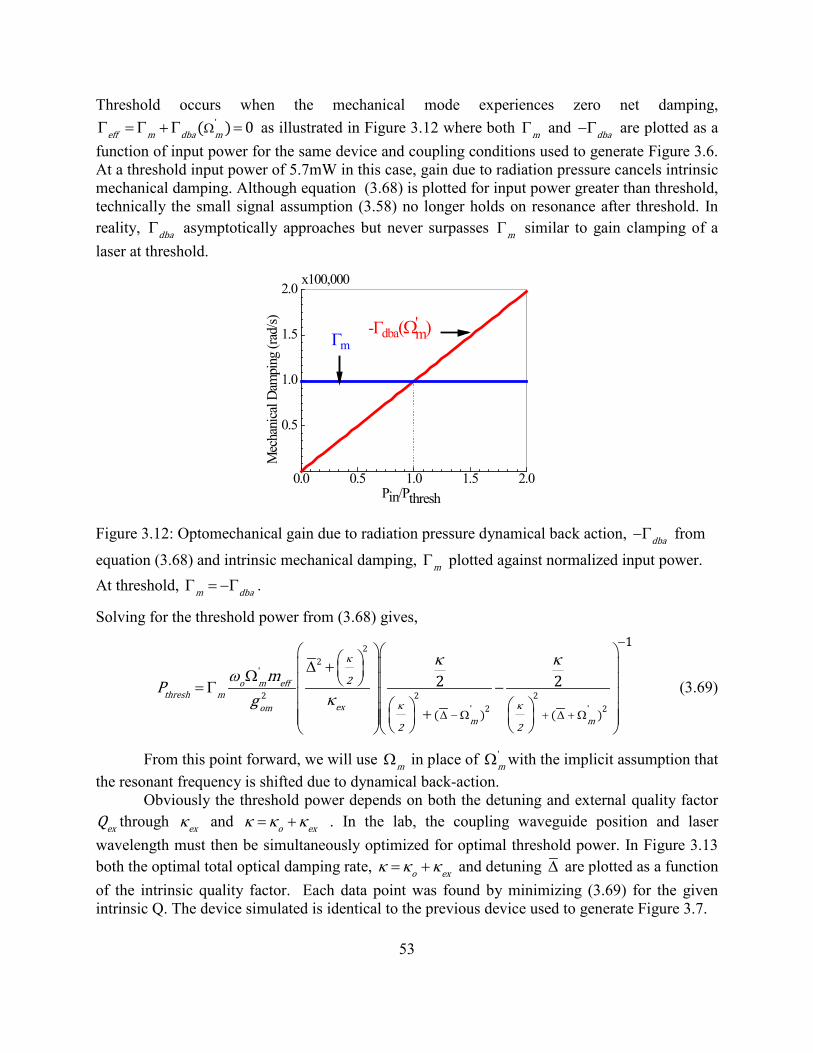
53
Threshold occurs when the mechanical mode experiences zero net damping, '( ) 0eff m dba mΩΓ = Γ + Γ = as illustrated in Figure 3.12 where both mΓ and dba−Γ are plotted as a
function of input power for the same device and coupling conditions used to generate Figure 3.6. At a threshold input power of 5.7mW in this case, gain due to radiation pressure cancels intrinsic mechanical damping. Although equation (3.68) is plotted for input power greater than threshold, technically the small signal assumption (3.58) no longer holds on resonance after threshold. In reality, dbaΓ asymptotically approaches but never surpasses mΓ similar to gain clamping of a laser at threshold.
0.0 0.5 1.0 1.5 2.0
0.5
1.0
1.5
2.0x100,000
Γm
Mec
hani
cal D
ampi
ng (r
ad/s)
Pin/Pthresh
-Γdba(Ω'm)
Figure 3.12: Optomechanical gain due to radiation pressure dynamical back action, dba−Γ from
equation (3.68) and intrinsic mechanical damping, mΓ plotted against normalized input power. At threshold, m dbaΓ = −Γ .
Solving for the threshold power from (3.68) gives,
22
'
2 2 2' 2 ' 2( ) ( )
1
2 2o m effthresh m
exomm m
2
2 2
mP
g
κ
κ κ
κ κω
κ∆ − Ω + ∆ + Ω
− ∆ + Ω = Γ − +
(3.69)
From this point forward, we will use mΩ in place of 'mΩ with the implicit assumption that
the resonant frequency is shifted due to dynamical back-action. Obviously the threshold power depends on both the detuning and external quality factor
exQ through exκ and o exκ κ κ= + . In the lab, the coupling waveguide position and laser wavelength must then be simultaneously optimized for optimal threshold power. In Figure 3.13 both the optimal total optical damping rate, o exκ κ κ= + and detuning ∆ are plotted as a function of the intrinsic quality factor. Each data point was found by minimizing (3.69) for the given intrinsic Q. The device simulated is identical to the previous device used to generate Figure 3.7.

54
In Figure 3.13(a), it is evident that in the unresolved sideband regime, the waveguide gap should be chosen such that / ~ 1.3oκ κ or / ~ 0.75tot oQ Q for minimum threshold power. This slight undercoupling is to maximize the optical Q the light experiences while at the same time allowing enough light to enter the device. In the resolved sideband regime, the optimal device should be well overcoupled as the optimal coupling gives ~ mκ Ω and it is evident that the coupling Q should be continually reduced as the intrinsic Q increases. The device must be overcoupled so that the 0 mω − Ω phase modulation sideband is amplified by the cavity
Lorentzian while the o mω + Ω modulation sideband is highly attenuated. This asymmetry is
crucial to produce net light at frequency mΩ . The optimal detuning calculated in Figure 3.13(b) is ~ / 4κ in the unresolved sideband regime which maximizes the Lorentzian slope the laser samples. In the resolve sideband regime, the optimum detuning equals the mechanical frequency,
mΩ so that the lower modulation sideband is exactly on resonance with the cavity.
105 106 107 108 109
0.1
1
10
100Unresolved Sideband
Intrinsic Optical Q
Optim
al κ/
κ o
1
10
100Resolved Sideband
Optimal κ/Ω
m
105 106 107 108 1090.1
1
Intrinsic Optical Q
Optim
al ∆/
κ
1
10
100Unresolved Sideband Resolved Sideband
Optimal ∆/Ω
m
(a) (b)
Figure 3.13: (a) Optimal total optical linewidth, κ vs intrinsic optical quality factor. The optimal linewidth is normalized by the intrinsic linewidth (left axis) and mechanical angular frequency (right axis). (b) Optimal detuning vs intrinsic quality factor. Detuning is normalized by the total optical damping rate, κ (left axis), and angular mechanical frequency (right axis). Grey and green shaded areas of the graph delineate the unresolved and resolved sideband regimes.

55
Once the optimum detuning and total quality factor are known, the threshold power is then calculated for the given oQ as shown in Figure 3.14. In the unresolved sideband regime the
minimum threshold power is proportional to 3oQ . This is expected since in section 2.2.1 it was
shown that the circulating power scales with oQ and one can verify from equation (2.31) that the
maximum Lorentzian slope scales with 2oQ . Again, the Lorentzian slope is responsible for
asymmetry in the upper and lower phase modulation sidebands which mediate phonon creation in the cavity [48]. In the resolved sideband regime, the threshold power is independent of intrinsic optical Q which isn’t surprising since it was already shown that the minimum threshold power occurs when the total Q is on the order of mΩ regardless of the intrinsic Q. Also plotted in Figure 3.14 is the threshold power for different mechanical quality factor. As expected from the
mΓ dependence in (3.69), threshold power scales with 1mQ − regardless of oQ . Thus, high
mechanical Q structures are desired for low threshold power devices.
105 106 107 108 109 101010n
100n1µ
10µ100µ
1m10m
100m1
10 Unresolved Sideband Resolved Sideband
Qo<ωo/Ωm
1/Q3o
Qo>ωo/Ωm
Qm=100kQm=10kTh
resh
old
Powe
r (W
)
Intrinsic Optical Quality Factor
Qm=1k
Figure 3.14: Threshold power using optimized external coupling Q and detuning plotted as a function of intrinsic optical quality factor. The plot is parameterized by the intrinsic mechanical quality factor. The threshold power trend with oQ changes around the barrier between the resolved and unresolved sideband regimes.
Approximate Behavior in the Unresolved Sideband Regime (USR) The approximate threshold power trend in the unresolved sideband regime may be
derived by assuming mΩ << ∆ . A first order Taylor expansion of the first term in parenthesis in equation (3.68) for ( )dba mΓ Ω gives,

56
2 2 2
2 2 20( )
21 1
m
m
m2 2 2
κ κ κΩ →+ ∆ + Ω + ∆ + ∆
∆Ω≅ −
Likewise,
2 2 2
2 2 20( )
21 1
m
m
m2 2 2
κ κ κΩ →+ ∆ − Ω + ∆ + ∆
∆Ω≅ +
Substitution into (3.68) yields after simplification,
2 2
22
3
2 | |( ) (Unresolved Sideband Regime)om in ex
dba meff
2
g sm
κ
κκΩ
∆Γ ≅ −
∆ +
(3.70)
It was already shown in Figure 3.13 that optimal ,exκ κ and ∆ are all on the order of oκ
in the unresolved sideband regime (USR) so equation (3.70) demonstrates that ( )dba mΩΓ scales
as 3oκ − or 3
oQ . This result is also important in noise contexts as it shows that the small signal gain
( )dba−Γ scales with 3oQ close to resonance for blue detuning. Higher oQ devices in the
unresolved sideband regime thus amplify external forces (such as noise) more than lower oQ
devices. Also, equation (3.70) shows that for low oQ devices the optomechanical gain is frequency independent for frequencies close to the resonance frequency thus confirming the observed trend in Figure 3.11.
Assuming the device coupling and detuning are chosen to minimize threshold power, Figure 3.13 suggests that the following values should be substituted into (3.70): / ~ 4 /3oκ κ ,
so / 1 /3ex oκ κ = , and / 1 / 4 / 1 /3oκ κ∆ = → ∆ = . Substitution gives,
2 2
thresh3
3 | |6( ) (For Minimum P in USR)5
om indba m
eff o
g sm κ
Ω
Γ ≅ −
(3.71)
Setting equation (3.71) equal to m /m mQ−Γ = Ω and solving for 2| |in c inP sω≅ yields the approximate minimum threshold power,
4
thresh,min 2 3
35 (in USR)6
eff c m
om o m
mP
g Q Qω Ω
≅
(3.72)
Equation (3.72) was verified to be in excellent agreement and within ~5% deviation from the data plotted in Figure 3.14 in the (USR). Quick inspection of equation (3.72) confirms both the

57
3oQ − and 1
mQ − dependence of threshold power. The 2omg − dependence also reveals that large
optomechanical coupling is an important metric in reducing threshold power. The threshold power also scales linearly with mechanical frequency. Finally since the mechanical stiffness is to first order independent of radius and 2
effm R∝ , then 1m R −Ω ∝ (equation (3.22)). Inserting
equation (3.9) for /om cg Rω≈ − , then means 3threshP R∝ . Smaller devices still in the USR are
expected to produce the smallest threshold power. Indeed, a 1μm silicon resonator exhibited a low threshold at a dropped power of 3.6μW [52]. Accounting for the cavity transmission of 96%, the corresponding threshold power is larger but cannot be discerned from the given parameters. Our group has fabricated a 20μm Silicon resonator with oQ =1 million having an ultralow threshold power of just 17μm. This device will be further explored in chapter 5.
Approximate Behavior in the Resolved Sideband Regime (RSR) Continuing with the resolved sideband regime, since the detuning, total Q and intrinsic Q are all on the same order, no convenient Taylor expansion of equation (3.68) is readily apparent. It was already shown that the optimal detuning is m∆ = Ω . One can then skip to the assumption that the device is excited by a laser set to the optimal detuning for low threshold power, m∆ = Ω
found previously. Aided by Figure 3.13 we also assume that ~exκ κ and 2 2 2( / 2) ~m mκ + Ω Ω to find, 2 2
thresh3
| |( ) 2 (For Minimum P in RSR)om in
dba meff m
g sm
ΩΓ ≈ −Ω
(3.73)
4
thresh,min 2
1 (in RSR)2
eff m c
om m
mP
g QωΩ
≈ − (3.74)
The threshold power calculated from equation (3.74) matches the cases in Figure 3.14 within 10% in the deeply RSR but is off by as much as a factor of 3 for intrinsic optical Q’s which are only moderately sideband resolved. Nonetheless, the general threshold power features are adequately captured by equation (3.74). Minimum threshold power is observed to be independent of oQ and again inversely dependent on mQ . Thus, in both regimes, the threshold power is improved with larger mechanical quality factor. The circulating power and Lorentzian slope still scale as totQ and 2
totQ respectively but in the RSR regime, the optimal totQ scales with 1
m−Ω so threshP scales with 3
mΩ multiplied by an additional factor of mΩ reflecting the mode stiffness similar to the case in the USR. Almost all devices tested in this thesis are either firmly in the unresolved regime, while in PSG we were able to approach the border of the two regimes.
3.6.2 OMO Noise and Phase Noise Spectrum Now that the design space for low power and large signal OMO’s has been covered, the
noise properties will be explored. In deriving the carrier power, it was assumed that the RF

58
power in the fundamental sideband was concentrated at a single angular frequency, mΩ . Thus, the OMO output power would be a perfect sinusoid,
( ) sin( )out o mP t P t= Ω
possessing a Fourier transform consisting of delta functions at m±Ω in frequency space. Of course this is not physically realizable since delta functions don’t normally occur in nature. In reality, noise perturbs the oscillating system momentarily changing its output phase from tmΩ to t (t)m ϕΩ + and its amplitude from oP to (1 ( ))oP tα+ where ( )tϕ and ( )tα are random time varying signals with assumed amplitudes much smaller than unity [53]. The output of the OMO becomes,
( )( ) (1 ( ))sin ( )out o mP t P t t tα ϕ= + Ω +
where mΩ now represents the average output frequency. Since the output frequency is the derivative of the instantaneous phase, the instantaneous frequency in the presence of noise becomes,
( ) ( )o mt tϕΩ = Ω +
It is now apparent that the output sideband power is no longer a delta function, but is spread out in frequency about the average frequency, mΩ . Figure 3.15 demonstrates how slight phase slips affect the apparent zero crossings of a nominal sinusoid and alters the frequency spectrum interpreted from the spacing between zero crossings. Note that frequency noise rather than phase noise could have been tracked. Phase noise is more popular in oscillators where associated electronics depend on the short term phase characteristics, while frequency noise or jitter is important in clocks where the long term (>1s) frequency stability is relied upon.

59
(a) (b) Figure 3.15: (a) An ideal oscillator with perfect sine wave output and frequency spectrum given by a delta function centered at the stationary inverse angular period. (b) Real life oscillator output with jitter due to noise. The period measuring at the zero crossing is no longer stationary and thus the frequency spectrum is spread out around the average frequency. This figure originates from the Nguyen group.
In OMO’s, noise may originate from shot noise in the pumping photons (quantum noise), thermal noise (Brownian motion) of the mechanical resonator, relative intensity (RIN) and frequency noise of the laser, environmental noise such as table vibrations or temperature fluctuations, or thermal variation of the refractive index (thermorefractive noise) [54]. Dark current in the photodetector due to thermal (Johnson), and generation recombination noise (G&R) as well as input noise in any signal analyzers are typically lumped together as electronic noise. At frequencies far from resonance, electronic noise may dominate in low power systems where shot noise is negligible. If the detector is followed by an RF amplifier, the amplifier adds some noise to the signal quantified as the noise figure, /in outNF SNR SNR= . An Erbium Doped Fiber Amplifier (EDFA) which may be utilized to boost the pump power will also contribute amplified spontaneous emission (ASE) noise. In optomechanics, shot noise in the cavity photons results in a fluctuating radiation pressure force resulting in an apparent noise in the displacement causes further photon number fluctuation. This noise is deemed quantum back action noise and together with Brownian motion noise sets a fundamental limit on the system noise [55]. There are undoubtedly other noise sources in OMO’s not mentioned here. Known noise sources in a typical characterization setup are summarized in Figure 3.16. A full model taking all these noise sources into account is beyond the scope here. We focus on Brownian noise since it dominates at certain frequency offsets from the carrier [56] as well as shot noise and electronic noise.

60
Figure 3.16: Possible noise sources in a typical OMO characterization setup. EDFA= “Erbium Doped Fiber Amplifier.”
While in general, it is desirable to have minimal amplitude noise oscillator designers focus on phase noise for a couple reasons: 1) When an oscillator serves as a frequency reference, the phase of its output is usually relied upon rather than the amplitude. This is especially the case in a Phase-Locked Loop (PLL) where an electronic system is locked to the phase of an oscillator reference and the behavior of the system is rather impervious to small deviations in the oscillator amplitude. In section 6.2, the noise properties of phase-locked loops will be derived in the framework of locking a voltage tunable OMO to an RF frequency reference. 2) Typical oscillators have an amplitude limiting mechanism which quells any amplitude fluctuations in the system [57]. Equipartition theory of thermodynamics predicts that a thermal noise limited oscillator will produce equal amounts of noise in its phase and amplitude quadratures, however since the amplitude noise is highly suppressed, it is the phase noise which dominates in the resulting output waveform [57]. The phase noise is then simply half the total noise derived in the absence of amplitude noise attenuation.
Output Noise Derivation To derive the noise spectrum in the OMO output power, the small signal model of the previous section is utilized. While the small signal model doesn’t hold above threshold at resonance where the time varying components in (3.58) are large, small signal theory should hold quite well just offset from resonance. Recall that the oscillator effective 3dB linewidth is given by ( ) ( )eff m m dbaΓ Ω = Γ + Γ Ω which is very close to zero at threshold. Since Figure 3.11
showed that ( )dbaΓ Ω is relatively flat around mΩ especially in the USR, the effective linewidth is very close to zero such that just outside of resonance any time varying signals are small in comparison to their steady state value. Indeed we, along with other groups have measured above threshold OMO linewidths to be less than 10Hz and at times less than 1Hz [56], while [58] and [52] measured typical linewidths less than 1KHz. It is safe to assume that the theory presented here then should hold at frequency offsets of 1KHz or more and likely even smaller offsets for the high performance OMO’s characterized later in this thesis.

61
The output field noise resulting from input noise sources begins by substituting equation (3.58) into (3.19),
( )s ( ) ( ) ( )out out in in exs t s s t a a tδ δ δ κ+ = + − +
After applying the steady state relation,
out in exs s a κ= −
and a Fourier transform, the output field noise is,
s ( ) ( ) ( ) .out in exs aδ δ δ κΩ = Ω − Ω (3.75)
We now re-write the top equation in (3.60) but this time add a term, ( )qn os tδ κ for the quantum field noise entering the cavity through its intrinsic loss port in addition to the already present term, ( )in exs tδ κ for noise entering through the input terminal,
( ) ( ) ( ) ( ) ( ) .
( ) ( ) ( )( )
( )
om in ex qn o
om in ex qn o
i a i a ig a x s k s t2
ig a x s k s ta
i2
κδ δ δ δ δ κ
δ δ δ κδ
κ
Ω Ω Ω Ω
Ω ΩΩ
− Ω = ∆ − − + +
− + +→ =
− ∆ + Ω
(3.76)
Substitution of (3.76) into (3.75) then gives,
( ) ( ) ( )
s ( ) ( ) .( )
om in ex qn oout in ex
ig a x s k s ts
i2
δ δ δ κδ δ κ
κΩ Ω− −
Ω = Ω +− ∆ + Ω
(3.77)
In equation (3.64) the displacement noise was eff exx Fδ χ δ= but this assumed a noiseless input
field, ( )in ins t s= . Keeping the input field noises in equation (3.63) we now arrive at,
( ) ( ) ( )eff ext eff dbax F Fδ χ δ χ δΩ = Ω + Ω (3.78)
A new force due to dynamical back action,
( ) ( )
( ) ( ) ( ) ( )( ) in ex qn o in ex qn o
dba om
i i2 2
s k s k s k s kF g a
κ κ
δ δ δ δδ
∗ ∗Ω Ω Ω Ω
− ∆ + Ω + ∆ − Ω
− −Ω
+ + = − +
(3.79)

62
arises from photon fluctuation-induced noise in the cavity displacement. Writing the displacement noise, ( )xδ Ω as a function of force into equation (3.77), we arrive at the output field noise,
( )( )
s ( ) .( )
om eff ex dba in ex qn oout in ex
ig a F F s k s ks
i2
χ δ δ δ δδ δ κ
κ
Ω + − −Ω = +
− ∆ + Ω (3.80)
The Fourier frequency, Ω , was dropped from all the dynamical noise terms for brevity. The power exiting the cavity as a function of time is,
( )
2( ) ( )
( ) ( )out o out out
out o out out out out
P t s s tP s s t s s t
ω δ
ω δ δ∗ ∗
= +
= + +
where the 2| |outsδ term was assumed negligible in the small signal approximation. Applying a Fourier transform to the time varying terms above gives the noise in the output photon power as a function of frequency [59],
( )( )( ) s ( ) s ( )out o out out out outP s sδ ω δ δ∗∗Ω = Ω + −Ω (3.81)
and corresponding power spectral density (PSD) for the special case of frequency independent noise components,
( ) 22s spp o out out out outS s sω δ δ∗ ∗= + (3.82)
However, equation (3.80) implies some frequency dependence due to the frequency dependent effective susceptibility, ( )effχ Ω and the weak dependence on Ω in the denominator which is
negligible in the unresolved sideband regime but may be significant in high oQ devices where the detuning is on the same footing as the mechanical frequency.
Following the able lead of Fabre [59], the output single sided noise power spectral density ( )ppS Ω [watts2/Hz] is formally determined from its correlator,
( )'( ) ( ) 2 ( ') ( ).out ppP P Sδ δ πδ∗
Ω Ω− = Ω − Ω Ω (3.83)
Integrating (3.83) would then provide the desired PSD provided the constituent correlators are known. For now, we consider shot noise, and the fluctuating thermal Brownian force with respective correlators,
( ) ( ) ( )
( ) ( )
' '
'
( ) ( ) ( ) ( ) 2 '
( ) ( ) 2 ' 2
qn qn in in
th th m eff B
s s s s
F F m K T
δ δ δ δ πδ
δ δ πδ
∗ ∗
∗
Ω Ω Ω Ω
Ω Ω
− = − = Ω − Ω
− = Ω − Ω Γ
(3.84)

63
where BK is Boltzmann’s constant, and T is the temperature. Note that the white thermal force power spectral density ( ) 2FF m eff BS m K TΩ = Γ [N2/Hz] applies in the classical limit of mT >> Ω[60] which is easily satisfied at room temperature. Application, of equation (3.64) to the bottom equation in (3.84) shows that the optomechanical resonator shapes the white thermal force through the effective susceptibility such that the displacement noise PSD in the absence of an optical field is [54],
( )( ) ( )
2
0
22 22
( ) |χ | 22
( )
inxx m m eff BP
m B
eff m m
S m K TK T
m
=
Ω
Ω = ΓΓ
=Ω − Ω + ΩΓ
(3.85)
By pumping at lower power, the laser samples the power spectral density with width mΓproviding a convenient means for deducing the intrinsic mechanical quality factor. One can confirm that in the limit of 1mQ >> , ( )effχ Ω is a Lorentzian as long as the resonator is operated below threshold [61].
To find the PSD of the output noise we integrate (3.83), in conjunction with (3.81), and (3.80). We assume that the quantum and thermal noise contributions are uncorrelated such that (3.84) represents the only non-zero correlators. We also assume that input noise from the waveguide and from the intrinsic loss are uncorrelated. There are many cross-terms in the evaluation of equation (3.83), but output noise due to quantum back-action can be assumed negligible when compared to Brownian motion noise at room temperature [37][54]. Keeping only the most dominant terms results in,
( )*2 2 ( )| | ( ) 2( ) 1 ...( )* .
( ) ( )
effom eff m eff B o expp o out ex
g a m K TS P
i i2 2
χχ κ κω κ
κ κ
ΩΩ − Γ + + Ω ≅ + + −Ω
− ∆ + Ω + ∆ − Ω
(3.86)
where the …( )*−Ω implies that the equation is repeated with Ω → −Ω and then conjugated. The first term in (3.86), o outPω , is recognized as the shot noise contribution while the term
containing effχ is the contribution from Brownian motion. For the effective susceptibility, it is
assumed that ( )dbaΓ Ω clamps at its threshold value such that ( ) ( )in thresh in thresh
eff effP P P Pχ χ
> =Ω = Ω .
The last two terms containing exκ and oκ are due to shot noise entering the cavity through the waveguide and intrinsic loss ports respectively which is then filtered by the cavity Lorentzian.
From previous arguments, the output power contains equal phase and amplitude quadratures but above threshold only the phase quadrature remains. The output power at phase modulation sideband, Ω is then,
64
pppp,
( )( )
2S
S ϕ
ΩΩ = (3.87)
The corresponding RF sideband PSD an ESA would see out of a photodetector is,
( )2
,vv, ( ) RF v o pp
L
G R T SS
Rϕ
ϕ Ω = (3.88)
With the same definitions for RFG , oT , VR , and LR as equation (3.55).
To investigate the dependence of the output noise on oQ and mQ , in Figure 3.17 the RF noise PSD as a function of offset frequency from resonance is plotted for various intrinsic optical and mechanical Q’s. This time the chosen device is a 25μm radius SiN OMO with
122.6 10 kgeffm −= × . As we’ll see later, this particular device has produced some of the best noise properties of any OMO [13]. In (a), the mechanical Q is fixed at 10.5k (a value we have reached in SiN vacuum) while the intrinsic optical Q is parameterized from a value of 70k up to 7M. For simplicity, the optical power was fixed at 2mW for all cases. It is evident that the output noise degrades as oQ increases. This is due to greater transduction of Brownian motion to optical
field noise. From equation (3.80), as oQ increases the stored optical energy quantified in a
increases which leads to a more efficient conversion from displacement noise, xδ , to outsδ . A
second dependency comes from the /exκ κ factor which steadily rises with oQ for optimal threshold power. As the device approaches more sideband resolved this factor becomes fixed as does the circulating power since eventually κ approaches mΩ and the noise degrades less rapidly with increasing oQ . It is also interesting to notice that the point where the noise curve
flattens occurs at a lower offset for lower oQ which is explained by smaller Brownian noise and
thus white shot noise becomes dominant at smaller frequency offset. The two highest oQ devices are Brownian noise limited for virtually all offsets with only a hint of shot noise appearing at ~1MHz offset. Electronic noise has not been taken into account, but it also contributes a flat portion to the noise spectrum and could dominate in low power devices where shot noise is small. In the inset of (a), the raw 74MHz noise peak is shown for the 70oQ k= case. As mentioned before, the small signal assumption breaks down and the curve is not accurate on, or close to resonance. Setting ( )~ 0meff ΩΓ to produce the plots leads to a singularity at mΩ in the effective susceptibility which makes the noise peak artificially ascend towards infinity.
In Figure 3.17(b), the mechanical Q is parameterized while oQ is fixed at 70k and again
the input power is 2mW. The output noise appears proportional to 1mQ − in the sloped
20dB/decade portion of the spectrum. This is due to reduced Brownian noise mostly arising from the mΓ factor in the thermal force PSD, FFS (equation (3.84)). As the output RF noise is proportional to FFS the noise drops off linearly with increasing mΓ . A higher mechanical Q

65
resonator stores mechanical energy longer and therefore acts as a better filter against off-resonance thermal noise. Thus high mechanical Q devices are expected to produce lower output noise devices and in the previous section they simultaneously produced lower threshold power - a win-win for both noise and power.
102 103 104 105 106 10710-2410-2310-2210-2110-2010-1910-1810-1710-1610-1510-1410-1310-1210-1110-10
73.50 73.75 74.00 74.25 74.50
10-18
10-13
10-8
10-3
RF P
ower
(A.U
.)Frequency (MHz)
Qo=7M Qo=700K Qo=70kOu
tput
Noi
se P
SD (W
2 /Hz)
Frequency Offset (Hz)102 103 104 105 106 10710-24
10-2310-2210-2110-2010-1910-1810-1710-1610-1510-1410-1310-12
Qm=1k Qm=10k Qm=100k
Outp
ut N
oise
PSD
(W2 /H
z)Frequency Offset (Hz)
(a) (b)
Figure 3.17: Single sided oscillator output noise spectrum as a function of frequency offset from the carrier at 74MHz. (a) The intrinsic optical Q is parameterized and ranges from 70k to 7M. (b) Parameterized mechanical Q from 1k to 100k. In each case, κ and ∆ were optimized for minimal threshold power.
3.6.2.1 Phase Noise Spectrum In oscillators, the most quoted figure of merit pertains to the one-side power spectral
density of the oscillator output phase, ( ) PSD of (t)Sϕϕ ϕΩ = with units [radians2/Hz]. A log-log plot of this spectrum as function of frequency offset from resonance reveals rich information about the oscillator noise properties and is henceforth referred to as the phase noise spectrum [53],
( ) ( ')' 10
2S f
f Log ϕϕ
=
L (3.89)
where ' of f - f≡ is the offset frequency from carrier, of . The phase noise is quoted as [dBc/Hz] or decibels below the carrier in a one Hz bandwidth and may be specified at a particular frequency offset – 1kHz and 10kHz offset are convenient. It is important to point out that this is not the same as the noise in a sideband of the output power which was previously calculated and plotted for various cases above. Fluctuations in the oscillation phase lead to a perceived change in the oscillator output power - the spectrum of which is calculated in equation (3.87) in the optical domain and (3.88) in the RF domain. However, it can be shown that for small fluctuations in the phase, or equivalently short time scales where the phase doesn’t drift appreciably, the phase noise spectrum of (3.89) is approximately [53],

66
( ) ,
,
( ')1' 102 (@ )
vv
sig RF m
S ff Log
Pϕ
≅ Ω
L (3.90)
where ,sig RFP is the carrier or signal power at fundamental frequency, mΩ calculated in equation
(3.55). vv, ( ')S fϕ is the PSD of the output power due to phase fluctuations at frequency 'f away from the carrier given by equation (3.88). The validity of (3.90) is understood from Figure 3.18 where a small perturbation in power Pδ is added to the carrier signal ( )sigP t rotating in the
complex plane with noiseless amplitude and phase given by| |sigP and tω respectively. In the
presence of a noise source, the amplitude and phase become | | | |sig sigP Pδ+ and tω ϕ+
respectively. Imagine translating ( )sigP t to the real axis momentarily: The component of Pδ
due to the instantaneous shift in phase is approximately, | |sigP Pϕδ ϕ⋅ as long as ϕ is small.
We can thus express the PSD of the phase as ,/PP sig RFS S Pϕϕ = reconciling equations (3.89) and (3.90). For thermally limited oscillators like OMO’s [56], any input noise induces equal amplitude and phase components to the output noise so that / 2P Pϕδ δ= . Equation (3.90) also presents the figure of merit intuitively as a noise to signal ratio – smaller is better. Unless noted otherwise, the noises are by convention, taken to be single-sided for phase noise purposes.
Figure 3.18: Illustration of periodic carrier signal ( )sigP t rotating in the complex plane at rate ω with perturbation Pδ tacked on due to noise. The resulting change in power due to the noise induced phase shift, ϕ , is approximately | (t)|sigP Pϕδ ϕ⋅
Since the phase noise spectrum constitutes a primary means of judging OMO quality, many spectra will be shown throughout the rest of this thesis. It is worthwhile to highlight the primary regions of a typical spectrum along with their physical significance. Figure 3.19 presents

67
the measured phase noise of a high performance 18.6MHz PSG resonator [62]. To acquire the spectrum below, light exiting the OMO was photodetected, amplified and analyzed with an Agilent E5500 phase noise measurement system. Saving some of the details of the phase noise measurement apparatus for later, we presently call attention to the various slopes in the spectrum. For frequencies above ~500kHz the spectrum is flat. Then it follows a 20dB/decade slope until about 1kHz offset at which point the spectrum rises 30dB/decade and even close to 40dB/decade slope at some points. The inset of the graph displays the strong 18.6MHz peak in the output spectrum captured simultaneously by an electrical spectrum analyzer (ESA). The phase noise spectrum may be crudely understood as a normalized plot of the carrier shoulder which would ideally be non-existent in the absence of noise.
101 102 103 104 105 106
-140-120-100-80-60-40-20
0
1/f 3
Phas
e Noi
se, L
(f), (
dBc/H
z)
Frequency Offset (Hz)
1/f 2
18.50 18.55 18.60 18.65 18.70 18.75-120-110-100-90-80-70-60
Pow
er [d
Bm]
Frequency [MHz]
Figure 3.19: Phase noise spectrum of a 52.5μm PSG OMO with oQ =520k, mQ =1160,
2 18.6MHzm πΩ = ⋅ . Inset: RF spectrum of measured resonance in self-oscillation.
To gain some physical insight into the observed slopes in the measured phase noise spectrum, we turn to Figure 3.20 which includes several noise sources and their interaction with the oscillating system. Drawing intuition from equation (3.86) we see that input shot noise not entering the cavity is filtered by the relatively broad cavity transmission spectrum and exits the cavity through the waveguide. Since shot noise is flat in frequency, this component contributes to the flat, red portion of the phase noise plot (red). Some shot noise enters the resonator through the coupling waveguide or its intrinsic loss port. Upon entering the resonator, this shot noise is filtered by optical system Lorentzian and may exert a noisy force on the mechanical resonator through dynamical back-action. The thermal Brownian force intrinsic to the mechanical resonator is also white but is filtered by the mechanical effective susceptibility which has very small linewidth close to resonance. Away from resonance the susceptibility has a 21 / f slope and thus filtered Brownian motion contributes a 20dB/decade slope to the phase noise spectrum in blue below. The thermal Brownian noise is sampled by the cavity photons and is thus amplified by the photon number and filtered by the cavity Lorentzian before exiting the cavity. Usually the cavity Lorentzian is quite broad compared to the offsets considered and so has negligible filtering effect on the phase noise. Slow noise sources with an inherent 1 / f slope may also exert a force on the resonator and be filtered by the effective susceptibility thus contributing a 31 / f or 30dB/decade slope to the phase noise spectrum shown in green. Though

68
1 / f noise sources are concentrated at frequencies well below resonance (typically less than 10kHz), they mix with the strong mechanical carrier at mΩ and are up-converted to the carrier frequency. Slow noise sources may include thermal drift or temperature dependent refractive index (thermorefractive noise) [54].
Figure 3.20: Noise sources, their interaction with the self-oscillating mechanical filter, and the corresponding regions in the phase noise spectrum.
Leeson’s Equation A popular viewpoint for phase noise in electronic oscillators stems from Leeson’s
equation,
'
22
( ) 12 'eff oB
sig
fFK TS f
P fϕϕ
Γ = + ⋅ (3.91)
which fits the general trend of phase noise as a function of frequency offset, 'f from the carrier,
of . Though Lesson’s equation is based off the physical argument that a generic oscillator with
linewidth effΓ imposes a 21 / f filter on the incoming white noise with phase noise spectral
density 2 /B sigK T P , it doesn’t explicitly give an expression for the oscillator excess noise factor, F . Without knowledge of F and its dependencies, it isn’t immediately obvious on how to optimize the system. Researchers have fitted OMO’s with the Leeson model [63] and found that modeling follows the general trend [64] but no expression for F was provided. The Leeson equation also doesn’t provide the carrier power, sigP and thus is viewed as more of a fit method to OMO’s at the present time.
Equation (3.91) does, however, provide valuable insight into the behavior of oscillators for changes in mQ and of . For instance it reveals that oscillator phase noise scales with the resonant frequency squared and it is typical to translate the measured phase noise to a common
69
frequency, sf by subtracting 20log( / )o sf f from the raw spectrum. We also see that phase
noise scales with 2effΓ so it is not surprising that smaller oscillation line-width is always desired.
Usually, effΓ is proportional to mΓ and in [58] it was calculated that this is indeed the case in OMO’s at small frequency offset. Thus we would expect the OMO phase noise spectrum to scale with 2
mΓ at small frequency offset. In Figure 3.17, the theoretical output noise was shown to
scale with mΓ but in our modeling we have seen some trends of phase noise scaling with 2mΓ and
some instances in which it scaled linearly with mΓ .

70
4 State of the Art Single Material OMO’s: Silicon Nitride and Doped Glass
Optomechanical resonators have been built from many materials into diverse shapes and sizes. Initial high optical Q microtorroids consisting of laser-reflowed glass [20] spawned the cavity optomechanics field. Even though they lack excellent phase noise, glass microtorroids have served as a vehicle for OMO physics and applications [56][12][65]. New materials have also emerged including a micron-sized GHz frequency silicon disk [52] and a zero flicker noise silicon nitride ring [14]. High optomechanical coupling photonic crystal zipper OMO’s integrated with photodetectors have recently demonstrated harmonics to ~6.5GHz [66].
In this chapter, we demonstrate low phase noise silicon nitride OMO frequency combs and highlight experiments which affirm some of the predicted trends of the previous chapter. We chose a hollow-disk mechanical resonator pioneered by the Nguyen group [67] for its high mechanical Q and ease of design and manufacturing. Since high optical Q’s are achievable in glass, glass OMOs are easily self-excited and serve as a great material for studying OMO behavior. Furnace reflowed glass was thus used for initial experiments and proof-of-concept work before transitioning to silicon nitride. Free standing OMO’s with integrated waveguides and low threshold power are also demonstrated in glass with optical Q’s rivaling, and in some cases, surpassing competing non-OMO technologies which incorporate integrated waveguides. Experimental methods for characterizing relevant figures of merit are also presented. Standalone silicon OMO’s have demonstrated interesting properties and are reserved for the next chapter.
4.1 Hollow Disk Design and Fabrication In order to excite mechanical oscillations efficiently, the optical resonator boundary must
be allowed to expand freely with minimal damping. Excess mechanical damping reduces the mechanical Q, degrading the resonator’s ability to filter thermal noise and transduce optical energy. Hence, we chose a hollow-disk design [67] shown schematically in Figure 4.1(a) below. The hollow-disk design achieves a high mechanical Q by attaching thin spokes to the inner edge of a free-standing ring WGM cavity. The spokes meet at a floating center point that is connected to anchors in a clover-leaf fashion. The floating center-point design decouples acoustic standing waves from the anchors as much as possible. The optical ring is designed wide enough to prevent overlap of the peripheral circulating optical field with the spokes. A 15μm phosphosilicate glass hollow-disk resonator is demonstrated in the SEM micrograph of Figure 4.1(b).

71
(a) (b)
Figure 4.1: Hollow disk design (a) drawing and (b) SEM of a 15μm radius device fabricated with the SOI process described below.
OMO’s were fabricated with a wafer-scale process capable of producing a diverse set of devices all on a 6” silicon platform [68] . The two primary processes utilized to fabricate OMO’s are shown in Figure 4.2 for the specific case of reflowed phosphosilicate glass (PSG) resonators. In (a) the process begins by depositing approximately 1.9μm PSG by LPCVD onto a bare silicon substrate. A thickness of 1.9μm gave the highest optical Q as determined from swept laser and RF modulation characterization. The LPCVD process is similar to a typical deposition of silica except a small amount of phosphorous is flowed during the deposition. The device is then defined with 250nm resolution stepper-based lithography followed by dry etching with C4F8, H2, and He gases. An important property of PSG, is that its sidewalls may be smoothed by melting at temperatures significantly less than pure silica. For our Phosphorous concentration, the device melts at temperatures ~1000°C whereas glass softens at a much higher temperature of 1600°C. Several process splits were carried out to determine the optimal melting temperature and time and a 4 hr. reflow at 1050°C was settled upon. These conditions resulted in sidewall smoothing with minimal formation of bubble-like scattering centers within the bulk PSG. Karen Grutter investigated these bubble defects and eventually found that a combination of wet and dry oxidation after the initial deposition prevented bubble formation [21]. In contrast to laser reflow of silica which is more of a serial process, furnace reflow of PSG melts all devices on a chip simultaneously and is more practical from a large-scale manufacturing standpoint. Finally, the PSG is released in a XeF2 dry etcher which isotropically etches the underlying silicon substrate. As XeF2 etches Silicon with extremely high selectivity to oxide (~1000:1) it should have no measurable impact on the smoothed PSG. A second, untimed release process shown in Figure 4.2 (b) was also used to manufacture OMO devices. This flow was used to fabricate the PSG device of Figure 4.1(b). Beginning with a silicon-on-insulator (SOI) wafer, anchor vias are defined and etched into the top silicon. PSG is then deposited and oxidized filling the vias and covering the top silicon. The PSG layer is then defined, dry etched and released as before. Since, the anchors are now defined by PSG-filled vias, the anchors are untouched by XeF2 and are well-defined lithographically. This process is handy for fabricating small devices which are more sensitive to release timing. For further details on the microfabrication one is referred to [21].

72
(a) (b)
Figure 4.2: PSG fabrication processes. (a) Timed release (b) Untimed release SOI process. Further details are in the text and in [21].
4.2 Tapered Microfiber Pulling Usually, OMO’s were interrogated with a tapered microfiber consisting of a bare single
mode fiber thinned down to a diameter of ~1μm [55,56]. Combined with a tunable laser, the tapered microfiber allows for a flexible coupling distance so that parameters such as threshold power and phase noise may be easily optimized during testing. In order to thin the fiber from its standard 125μm diameter down to 1μm, first a ~1cm portion of the protective jacket material is stripped either by hand or with a specialized tool. The fiber is then heated with a Propylene gas torch mounted on an electronically controlled translation stage. Simultaneously, the fiber is stretched on its long axis by two more counter-moving linear translation stages as shown in Figure 4.3(a). During pulling, the core material is displaced away from the flame as it gradually disappears into the cladding. 1550nm laser light is continuously fed into one side of the fiber and sensed with a photodetector connected to an oscilloscope on the output side. As the core diameter contracts, light transitions from a relatively large and diffuse fundamental mode in the core to a much smaller mode confined purely by the slightly lower index cladding. The transition from thick to thin fiber excites multiple modes which interfere at the photodetector. The fiber-length determines the relative phase of these modes and their superimposed power, so as the fiber is stretched, an oscillatory photocurrent appears on the oscilloscope. If the fiber pulling is prematurely stopped, the oscillatory signal disappears. When the minimum fiber diameter reaches ~1μm, only a single mode is supported at the fiber center, the oscillatory signal on the oscilloscope ceases, fiber pulling is immediately stopped by the operator, and the flame is retracted. All operations are controlled by a LabVIEW program originally written by Myung-Ki Kim. The fiber insertion loss after pulling is determined from the detector photocurrent before and after the process.

73
(a) (b)
Figure 4.3: (a) Tapered microfiber pulling setup showing flame torch in the vicinity of the fiber and linear translation pulling stages on either side. The fiber is magnetically clamped to fiber-launch platforms attached to the stages. (b) Transition from a traditional fiber-optical cable to a thinned microfiber.
To pull fibers with high transmission, the flame size was adjusted until most of the flame was blue in color except for the very tip closest to the fiber which possessed a small orange-colored dome-shape. The flame to fiber distance was adjusted until the fiber appeared to have a blue glow in the flame-vicinity when the room lights were dimmed. If the flame-size was not hot enough (typically a pure blue flame) or it was too far from the fiber, the fiber pulling would complete in less time and often the fiber would break during pulling. In this case, the fiber melt rate was not sufficient for the rate at which it was being stretched. If the flame was too close or too hot (more orange colored flame), the fiber would pull but would not be taught after the pulling run. In this case, the fiber melting rate was too fast when compared to the rate at which it was being stretched and the fiber would gradually sag as a result. Fibers were pulled at a translation stage rate of 15μm/sec which gave more consistent transmission without breakage when compared to faster pull rates. At rates less than 15μm/sec it was more difficult to avoid fiber sagging. It was also important to gradually retract the flame a total of ~150μm after about 10 seconds, likely because the fiber temperature needed to be hot to initialize melting, but once melting began, the same temperature melted the fiber too quickly. At the aforementioned 15μs pull rate (from both ends of the fiber), a typical run took three minutes, and the fiber was stretched by 4mm on each side. Transmission above 50% was readily attainable while we usually aimed for 60% transmission to deem the fiber adequate. A higher-end torch with larger flame size would likely yield higher transmission. With practice, a successful tapered microfiber could usually be manufactured in the span of a few hours. Reference [71] is an excellent resource for optimizing a tapered microfiber pulling apparatus.
4.3 Measurement Setup After pulling, the tapered microfiber was connectorized with a fusion splicer, epoxied to
a fixture incorporating single-axis tension-adjustment stages (Figure 4.4(b)) and transferred to the characterization setup. Wafers were diced into ~4mm wide die (Figure 4.4 (b)) so that the tapered fiber could approach the device plane without obstruction from the substrate. Test die were mounted on a metal finger holder and placed on a triple axis Thorlabs Nanomax piezo stage

74
incorporating an APT BPC203 piezo controller. Devices could also be tested in vacuum where the tapered fiber was mounted to a smaller form factor Attocube piezo stage with ANC350 10nm resolution controller. Figure 4.4(b) shows the tapered fiber while aligned to spoked hollow-disk resonator. Stiff, all-metal fixturing along with a plexi-glass enclosure proved critical to preventing drift of the fiber during testing. A typical tapered microfiber could last for months, but we found if continually kept in the atmospheric setup, its transmission slowly degraded with time. An IPA squirt followed by brief dry could bring the transmission closer to its original value. In our separate vacuum setup, the fiber transmission was stable over several months of usage even though the fiber was not in vacuum by default. It is believed that the smaller vacuum chamber is a cleaner environment that curtails microdust accumulation which has been observed on silica microspheres [36].
(a) (b) (c)
Figure 4.4: (a) Atmospheric test setup with tapered fiber holder incorporating tension adjustment stages. (b) Up close view of tapered microfiber and diced die. The microfiber is excited by a red laser for demonstration purposes showing that the evanescent field leaks out at the center of the fiber. (c) Microscope image of tapered microfiber adjacent to a PSG hollow-disk. The rough background surface is typical of a silicon substrate after etching with XeF2 without an initial native oxide removal.
The tapered fiber was typically aligned to the device with the broadband source method described in in chapter 2. The longitudinal axis positioning of the tapered fiber with respect to the device was found important for maximizing the coupling efficiency to high oQ modes. Thicker devices especially in PSG required a thicker portion of the fiber to be adjacent to the device for proper phase matching. In SiN, the thinnest portion of the fiber, which is readily identified by a red laser, gave the best coupling efficiency. Likewise, the vertical position of the fiber taper was also important especially in PSG disks which exhibited gently sloped sidewalls. In order to access the high Q modes, the tapered fiber was aligned along the sloped portion of the sidewall where less light interacts with the slightly rougher bottom corner. Figure 4.5 (a) illustrates this scenario along with the smooth PSG sidewalls. In SiN and silicon, the tapered fiber could be aligned at the device periphery since these materials are not reflowed.
After coarse alignment with the broadband source, finer alignment ensued. High resolution swept laser scans with an Agilent 81682A tunable laser and 8153A light meter identified the highest Q modes. Optical Q was typically measured with the swept laser technique while RF modulation technique was utilized when necessary. The optical power was kept low,

75
typically ~15μW from the laser to minimize thermal broadening of the optical resonance. To determine the intrinsic Q, the tapered microfiber position was stepped away from the device in ~20nm increments after each wavelength sweep until the far undercoupled regime was reached and ~tot oQ Q . Eventually, a LabVIEW program was written which automated the laser sweep, power readout, tapered fiber step-back and data fitting. At critical coupling, ideally the power on resonance drops to zero but noise and slight imperfections in the polarization, and fiber positioning limit the on-resonance extinction ratio. Thus, the extinction ratio at critical coupling is one way of quantifying the coupling quality. In Figure 4.5 an example set of tunable laser sweep curves with varying tapered microfiber position is shown. In this case, the extinction ratio is 16.3dB at around critical coupling. There is also a clear redshift in the resonant wavelength as the fiber draws nearer to the device. The redshift is due to effective index loading of the cavity by the tapered microfiber which increases the resonant wavelength via equation (2.4).
1552.14 1552.16 1552.18
0.00
0.20
0.40
0.60
0.80
1.00
1.20
22.45um 22.25um 22.05um 21.85um 21.65um
Tran
smiss
ion
(A.U
.)
Wavelength (nm)
Qo=300k
ER=16.3dB
Piezo Position
(a) (b)
Figure 4.5: (a) Positioning of tapered fiber with respect to sloping device sidewall. Optical Q measurement using a tunable laser and tapered microfiber. At a piezo position of 22.45μm the device is overcoupled and becomes critically coupled when the fiber moves 20nm away. The extinction ratio is 16.3dB at critical coupling.
After optical Q characterization, the samples’ optomechanical properties were determined with the setup in Figure 4.6(a) below. A tunable laser was gradually aligned to the optical fringe from red to blue detuning until Brownian noise peaks appeared on the ESA. A fiber polarization bench controlled the detuning while an isolator prevented backscattered light from des-stabilizing the laser. For high threshold power resonances, an EDFA boosted the optical input power while an attenuator was sometimes used to prevent saturation of the photodetector. Although not shown, an RF attenuator was usually placed after the photodetector to prevent additional nonlinearities through saturation of the RF amplifier. Finally, the power at the coupling junction was deduced from a 99:1 splitter connected just prior to the tapered microfiber input. Assuming loss in the microfiber is exponential with distance, the power at the coupling

76
junction is then, 1%100junction tfP P T= where tfT is the fractional power transmission of the
tapered fiber and 1%P is the power emanating from the 1% splitter arm [45]. A calibration was habitually performed to document the fractional transmission. Throughout this thesis we define
in junctionP P≡ .
Figure 4.6 (b) presents representative ESA spectra of a 1.8MoQ = PSG hollow-disk OMO with 52.5μm outer radius. At low input laser power, three Brownian noise-induced peaks at frequencies of 11, 18, and 80 MHz were visible. At 20 Torr, the peaks exhibited mechanical Q’s of 5500, 7000, and 2,300 respectively determined from a Lorentzian fit of the output noise peak. In each case, the peaks disappeared if the laser was turned off or moved outside of the optical resonance. The 11MHz peak is identified as a flexural mode while the 18MHz peak is the radial breathing (RBM), or first contour mode which consists of outward radial displacements. The 80MHz peak, not visible in all devices is called a pinch mode since it results in out of phase movement of the outer and inner ring. i.e. when the outer ring is moving radially inward, the inner ring is moving radially outward similar to what would happen if one pinched the ring along it’s width. Of the three modes observed, only the 18MHz mode could be self-excited optomechanically. This is due to the large RBM displacement profile overlap with the circulating optical field resulting in higher optomechanical coupling and smaller effective mass. The 80MHz peak is also difficult to excite since it is stiffer and as we’ve seen, threshP scales with
mΩ .
18.39 18.40 18.41 18.42 18.43
-110-100-90-80-70-60-50-40-30-20
11.25 11.26 11.27
123456
79.60 79.70 79.80 79.9018.40 18.41 18.41 18.41 18.42
80MHz18MHz11MHzQm1=5,500
RF
Res
pons
e (A
.U.)
Qm3=2,300
Frequency (MHz)Frequency (MHz)
Qm2=7,000
Frequency (MHz)
Pin=360µWPin=58µW
RF P
ower
(dBm
)
Frequency (MHz)
Qo=1.8MQm=7000
(a) (b)
Figure 4.6: (a) Optomechanical characterization setup and (b)Top: 52.5μm radius PSG Mechanical Brownian noise peaks at 11MHz, 18MHz, and 80MHz probed with low power input power at 15 Torr. Lorentzian fitting yielded mQ of 5500, 7000, and 2300 respectively. Bottom: Brownian noise of the dominant radial breathing mode at 58μW input power (orange) and self-oscillation peak (blue) with 360μW input power.

77
After characterizing Brownian motion, the input power was increased from 58μW to 360μW which was just above the measured threshold power of 290μW in this particular case. At this power, the broad Brownian noise was amplified and the peak height, shown in blue above, was observed to rapidly increase - a signature of optomechanically-induced mechanical lasing, or self-oscillation. An increase in resonant frequency was also observed due to the optical spring effect quantified in dbaK . The theoretical threshold power for this device is 170μW with
2eff om m= where om is the rest mass. The factor of two difference in measured and actual
threshold power could be due to lower omg than the simplistic assumption /om cg Rω= − , since
a high oQ PSG mode may reside closer to the center of the device. It could also be due to the somewhat crude threshold power determination method used at the time the data was taken. Optimizing the coupling conditions for optimal threshold power and accurately determining the point where radiation pressure exceeds Brownian motion is a delicate process. In chapter 5, an improved characterization setup is introduced to more accurately characterize ultralow threshold silicon OMO’s. Phase Noise Measurement System
To measure phase noise, the oscillating signal was inputted into an Agilent E5500 phase noise analyzer. A schematic of the phase noise analyzer is shown below. Both the device under test (DUT) RF output and a synthesizer reference are fed into a phase detector, in this case a double balanced mixer followed by a low pass filter. Recall that,
( )1cos( ) cos( ) cos( ) cos( )2o r o r o rϕ ϕ ϕ ϕ ϕ ϕ⋅ = − + +
-the mixer output contains components at the sum and difference phase of the two oscillators. A low pass filter removes the sum term which oscillates at 2 mtΩ and outputs the difference term, cos( )o rϕ ϕ ϕ− ∆ assuming the phase difference between the two oscillators is small. A perfect synthesizer reference will contribute negligible phase noise to the system and so ϕ∆ is a direct measurement of the OMO phase as a function of time. Either an external ESA or internal FFT then plots the spectrum of the OMO phase noise, Sϕϕ . In case the frequency of the DUT drifts slowly with time, it is locked to the synthesizer reference which acts as a voltage controlled oscillator (VCO) within a PLL loop internal to the phase noise measurement system.

78
Figure 4.7: Phase noise analyzer schematic. The OMO phase noise is compared against an assumed stable reference with the same average frequency. DUT=Device Under Test. LPF=Low Pass Filter. FFT=Fast Fourier Transform. PLL=Phase Locked loop.
What follows are some subtleties with the phase noise measurement and some lessons learned:
• The phase noise analyzer only measures the worst of the DUT and synthesizer reference phase noises. Our low-phase noise multimaterial OMO in chapter 6 actually outperformed some synthesizers in certain frequency offset bands. In these cases, the phase noise spectrum was limited by the measurement system.
• We found that the OMO frequency comb presented issues with the phase noise system as some of the higher frequency components would mix with the synthesizer reference and cause discontinuous jumps in the measured spectrum. Adding a low pass filter with cutoff frequency just below the 2nd OMO harmonic eliminated this problem.
• As with any instrument, the phase noise system is only as good as its settings. In particular the PLL tuning constant should be set as small as possible while still maintaining phase-lock with the DUT otherwise extraneous phase noise is added to the system by a PLL which is too slow.
• The frequency synthesizer contains its own internal PLL which sets the synthesizer frequency output as some integer defined ratio of the clock frequency, / cm n f⋅ , where
,m n are integers and cf is the synthesizer internal (usually Quartz) clock frequency [72]. If a very low phase noise DUT is being measured, sometimes this ratio is not of adequate accuracy ( ,m n can’t be made arbitrarily high) to properly lock the DUT, and again the phase noise is limited by the reference. In such cases we had to utilize a separate mode of the phase noise system called Electronic Frequency Control (EFC). Suitable for measuring only very stable DUT’s, in EFC mode, the output of the phase noise system PLL directly controls the quartz oscillator within the synthesizer reference rather than the integers m and n . Since the quartz oscillator has limited tuning capability, the DUT center frequency cannot drift appreciably or else the system loses lock. Not all synthesizer VCO’s are able to be fine-tuned in this manner, but fortunately the two we most frequently used, an HP8663A and an HP8644B, did have such a capability. Figure 4.8 demonstrates that EFC is vital for measuring a low phase noise DUT such as the SRS384 signal generator. The DUT was measured both with and without EFC and at frequency offsets below 200Hz, the benefit of EFC is evident. At a 10Hz offset there is a

79
40dB improvement in the measured phase noise. Also, note that the DUT outperformed the phase noise reference at >10kHz offsets.
Figure 4.8: Measured phase noise of an SRS384 Signal generator with EFC (red) and without EFC (blue) superimposed on the SRS specification (grey). At offsets below 200Hz, EFC is vital to record an accurate phase noise spectrum of such a stable DUT.
4.4 High Optical Q PSG OMO’s We have already seen that glass doped with phosphorous (PSG) may be reflowed to
produce cavities with high optical Q on a wafer-scale. In PSG disks, our highest measured Q was 11.7 million but disks suffer from very poor mQ . PSG is advantageous in that it is simple to define spokes prior to reflow to fabricate higher mQ hollow-disk ring resonators with little degradation in optical Q. In hollow-disks we have attained Q’s of 8.0 million as evidenced in the RF intensity modulation curves in Figure 4.9 (a) for the 52.5μm radius ring shown in the SEM (b). The same device was also measured with the intensity modulator biased at quadrature yielding curves similar to Figure 2.9 (a). (fit)totQ at quadrature bias was 7.8M in agreement with the value obtained from the peak bias point fit. An 18.3MHz resonator enters the sideband regime when 10.5oQ > million, so the studied devices are very close to being sideband resolved.

80
6.50 6.60 6.70 6.80 6.90
0.0
0.5
1.0
1.5
2.0
2.5
6.60 6.65 6.70 6.75 6.800.00
0.05
0.10
0.15
0.20
0.25
0.30
Raw Fit
Qtot(Fit)=8.0 million Piezo 15.92 um Piezo 15.73 um Piezo 13.61 um Piezo 15.49 um
|S21
| (A.
U.)
Modulation Frequency (GHz)
Qo=8x10⁶
(a) (b)
Figure 4.9: (a) RF modulation measurement of optical Q in a reflowed PSG hollow-disk. A linear piezo controller stepped the fiber away from the device in-between each measurement until the device was undercoupled. Inset: Fitted peak when the tapered fiber was at its furthest from the device gave a total optical Q of 8 million. (b) SEM of 52.5μm radius device measured.
The high optical Q of PSG makes it an excellent material for understanding optomechanical properties, especially since multiple optical resonances of widely varying Q in the same resonator may be characterized to discern trends with oQ . It is also easy to initiate self-oscillation in reflowed PSG due to the high Q’s attainable. In this section, we used this property to purposefully reduce mQ without destroying the possibility for self-oscillation and then measured the effect on phase noise. Later, a vacuum setup was constructed which could test the same effect. Even though studies were performed as part of this work, the goal was always to create and measure the best phase noise OMO device with the lowest threshold power. At the time initial measurements in PSG were being made, it immediately surpassed performance of microtorroids and was only bested by silicon nitride OMO’s which had been reported earlier [14].
4.4.1 Trends with optical Quality factor The devices tested in this section are all of the timed release variety and follow the
fabrication flow in Figure 4.2 (a). To study phase noise dependence on oQ , three resonances within a free spectral range of the same resonator were measured in atmosphere. Each optical mode circulates at a slightly different location in the ring interacting differently with the sloped edges and thus has a different oQ . This method ensures that the mechanical quality factor, mQ is
conserved while isolating any effects on optical oQ . The measured device had a somewhat lower

81
mQ of 680 in atmosphere but showed typical 2 18.4MHzm πΩ = ⋅ . Optical resonances chosen exhibited optical Q’s of 5.3M, 2.3M and 300k. Initially, the detuning, ∆ , and external tapered microfiber coupling, exQ , were optimized for minimum threshold power. The results of the
threshold power measurement are presented in the table below. The highest oQ again exhibits close to 2x higher threshold power than theory consistent with the data from Figure 4.6 (b) which is attributed to smaller optomechanical coupling. For 2.3MoQ = , theory and experiment match
well, but at 300oQ k= the theory of the previous chapter grossly overestimates the threshold power. Obviously another unknown force is acting in parallel with radiation pressure. In the next chapter we attempt to rectify some of the discrepancy for silicon OMO’s. It is possible that electrostrictive, nonlinear, or free carrier effects also play a significant role in reducing the threshold power in PSG, and nitride for that matter.
Qo=5.3M Qo=2.3M Qo=300k
Pthresh(measured) 170μW 780μW 5.6mW Pthresh(theoretical) 100μW 880μW 353mW
Table 4.1: Measured and theoretical threshold power for 3 optical resonances with varying oQ .
Phase noise was then measured for each resonance with ∆ and exQ now adjusted for optimal phase noise. Input power was kept between 2-3 times threshold and set for optimal phase noise. The 300koQ = resonance required an EDFA to boost the laser power and excite the device. The best phase noise data as well as fits for each optical mode are shown in Figure 4.10 with measured input optical power indicated in the legend. Interesting behavior is observed especially for the highest 5.3oQ M= line. At offsets greater than ~100Hz it is clearly inferior to the 300k resonance especially at ' 100kHzf = where there is a 20dB difference in the two. Such behavior could be expected given the modeling captured in Figure 3.17 where the noise alone scaled approximately with 2
oQ in the USR. However, Figure 3.17 was generated under the
condition of equal input power for each value of oQ and coupling conditions optimized for lowest threshold power both of which are not the case here. Output power noise due to Brownian motion scales as 2 2
totinP Q from equation (3.86) and (2.31), so based on Brownian motion alone,
the 5.3M and 300K resonances should have about equal phase noises given the measured input powers and relative oQ . The 20dB difference in phase noise must then come from the carrier
power. In Figure 3.9 it was shown that the carrier power scales roughly as 2inP . The ratio of the
two input powers squared is -24dB which is close to the difference in measured phase noise. Overcoupling the 5.3M resonance to reduce totQ likely helped reduce the phase noise further.
Indeed, in order to get the model to fit, a value of / 8oκ κ= was required for the 5.3M

82
resonance. For frequency offsets below 20kHz, the 5.3MoQ = actually outperforms the other two resonances and the phase noise slope even flattens out at ~10kHz. The source of this behavior is unknown, but it could be due to cavity filtering of input noise that exceeds the Brownian motion noise. The high oQ resonance also displays no 1 / f noise signature even down to 10Hz offset.
101 102 103 104 105 106
-140-120-100-80-60-40-20
0
Inten
sity
[A.U
.]
Qo = 5.3MQo = 300k
Qo = 2.3M
L(f)
Phas
e Noi
se (d
Bc/H
z)
Frequency Offset (Hz)
Qo = 300k, Pin=5.7mW Qo = 2.3M, Pin=2.2mW Qo = 5.3M, Pin=340µW
1551 1552 1553
0.7
0.8
0.9
1.0
Wavelength
Figure 4.10: Measured phase noise for three optical resonances and superimposed fit. Inset: Broadband optical spectra with three measured optical resonances highlighted. Carrier frequency is 18.4MHz.
To arrive at the fitted curves in Figure 4.10, two primary parameters were necessary. The first accounts for the fact that insδ is not quantum limited in our case and in order to fit the curves an extra amount of input noise had to be added to the system due to laser input noise - likely relative intensity (RIN) noise. For the oQ =300k resonator more noise was necessary since it was also driven by a noisy EDFA. The second parameter, is the electronic noise which dominates the flat portion of the curve for the two highest Q resonances. Later, it was found for silicon resonators that adding an EDFA immediately before the detector, reduced the phase noise in the flat portion of the curve for low threshold, low power devices. After studying PSG, we quickly moved on to other materials with higher mQ and didn’t try the same procedure in high
oQ PSG resonators. As we’ve seen, the threshold power in low oQ PSG is much smaller than expected and so the modeling cannot be performed a priori since the noise values depend on the input power. Thus, to fit the curves, the input power was set to the measured power but it was still assumed that ~ 0effΓ as required by the threshold condition. In the modeling, the detuning
and coupling were adjusted, and the displacement amplitude, ox , carrier power, sigP , and noise,
( )ppS Ω was calculated for each setting. The fitting parameter values are given in Table 4.2.

83
Qo=5.3M Qo=2.3M Qo=300k κ (fit) κo/8 κo/2 3κo/4 Δ (fit) κ/8 κ/8 κ/4 δsin(fit) 7 7 600 Psig (fit) 4.6nW 150nW 5.2mW
Table 4.2: Parameters used to generate curve fits for Figure 4.10.
4.4.2 Trends with Mechanical Quality factor To investigate how phase noise is affected by mechanical quality factor, we performed
two independent tests. In the first, we purposefully reduced mQ of a PSG resonator by adding a drop of epoxy to one of the spokes large enough to short it to the adjacent anchor. After applying epoxy, oQ remain fixed at 850k but the mQ dropped from 1160 to 440 resulting in a ~10-20dB degradation in phase noise as shown below. An 8.5dB phase noise increase is expected from Leeson’s equation. Also, the lower phase noise curve, taken prior to application of epoxy was acquired with almost half the input power as the curve with epoxy. This experiment thus confirms the results of the previous chapter that both phase noise and threshold power are improved by scaling mQ to as high a value as possible. Following these measurements we were propelled into the hunt for maximal mQ , similar to successful efforts in traditional MEMS oscillators [73].
101 102 103 104 105 106
-140-120-100-80-60-40-20
0
No Epoxy: QM=1160, Pin=3mw
L(f)
Phas
e Noi
se (d
Bc/H
z)
Frequency Offset (Hz)
Epoxy: QM=440Pin=5.5mW
(a) (b)
Figure 4.11: (a) Phase noise of 18.3MHz PSG device before (blue) and after (black) application of epoxy to one of the spokes. (b) Picture of device with epoxy glob on spoke.
4.4.3 Vacuum Setup to Increase Qm Motivated by the promising results of Figure 4.11, means were sought to increase the
mechanical quality factor in our OMO’s. A well-known method to increase mQ in devices

84
limited by air damping is to place the sample in vacuum. If the intrinsic mQ is limited by a dissipation method such as anchor loss, vacuum would have negligible effect. The hollow-disk minimizes anchor loss by design and thus evacuation of damping gas particles through vacuum was expected to raise the mQ [13]. A custom vacuum setup designed by Tristan Rocheleau of the Nguyen group was constructed with this in mind. Small form factor Attocube piezo stages were used to control the tapered fiber position and vacuum fiber feedthroughs connected it to the external measurement setup. We found that to prevent tapered fiber breakage, the chamber should be evacuated slowly, and the optical power at the fiber input should be kept at ~50mW or less. A top view of the chamber and nanopositioning stages is shown in Figure 4.12 (a).
In Figure 4.12 (b) we present phase noise results from testing a 1.8 millionoQ = ,
18.3MHzmf = , PSG device in atmosphere and at 25 Torr. At 25 Torr the mechanical Q was raised from 1200 to 7,200 and the measured phase noise was reduced accordingly this time by as much as 15dB. For offsets below ~300Hz the two phase noises are equal indicating that another noise source dominates in this region. Similar to the previous experiment, the required input to reach optimal phase noise was also reduced by more than a factor of two yet again confirming that mQ is vital to achieving low noise, low power OMO operation. For comparison, the measured phase noise of a 52MHz microtorroid from [58] is superimposed in red. At atmosphere, the two phase noises are similar below 3kHz at which point the PSG OMO proves superior. The input power wasn’t specified for the microtorroid case but based on other data in the reference, it is likely in the 1mW range.
102 103 104 105 106-140
-120
-100
-80
-60
-40
-20
760 Torr: Microtorroid[Zadeh, et al 2006]
25 Torr: Qm=7,200Pin=900µWL(
f) Ph
ase N
oise
(dBc
/Hz)
Frequency Offset (Hz)
760 Torr: Qm=1200Pin=2mW
(a) (b)
Figure 4.12: (a) Top view of Vacuum chamber with tapered microfiber loaded. (b) Phase noise of 18.3MHz PSG OMO in vacuum and atmosphere. Red curve is 52MHz Microtorroid OMO normalized to 18.3MHz for comparison [58].
In summary reflowed glass, or PSG is capable of achieving low threshold power operation, we observed as low as 170μW in atmosphere. This value is expected to reduce by a factor of six in vacuum given the observed mQ scaling. Threshold power as low as -83dBc/Hz

85
was shown here at 1kHz offset, and -110dBc/Hz at 10kHz offset with an 18.3MHz carrier. Further optimization of the reflow conditions, etching and release could lead to a sideband resolved OMO. High optical Q of 5.3 million was observed to flatten the phase noise at intermediate offsets and yielded no 1/f noise at small offset. In PSG, we have achieved optical Q as high as 11.7 million in disks and 8 million in hollow-disk OMO’s using a wafer-scale fabrication process.
4.5 PSG with Integrated Waveguides for On-Chip, Low Power Oscillators and RF Combs 4.5.1 Introduction
Dense integration is always desired in electronics and photonics and an ideal device should have the ability to be integrated with other components on the same chip. OMO’s are no exception. A particular limitation in integration is power consumption since usually integration is prompted by the demand for a mobile platform. A bulky, power hungry oscillator would negate the advantage of a single chip performing multiple functions normally carried out by isolated instruments. Thus it is desired to integrate OMO’s with coupling waveguides using a wafer-scale process without negatively affecting the oscillator performance.
Several groups have reported integrated optomechanical systems with on-chip waveguides [66],[71–74] and some have even integrated Germanium photodetectors, [78], [66]. However, of those mentioned, only [66] and [77] have demonstrated self-oscillation . In [66], a 112MHz photonic crystal zipper cavity OMO was reported with an excellent phase noise of -125dBc at 10KHz offset and -108dBc/Hz at 1kHz offset using 400μW dropped power. The reported optomechanical threshold occurred at 127μW dropped power. Since the coupling conditions were not given, it isn’t clear what the true threshold power is at the coupling junction. The reported mechanical Q of 480 was also quite low likely due to large anchor loss of the photonic crystal design. In [77], a 42MHz silicon nitride OMO with integrated waveguides was reported with phase noise of -108dBc/Hz at 10KHz offset and -93dBc/Hz at 1kHz offset using 32mW of power from the laser (the power at the coupling junction was not specified). Since the material was SiN, it exhibited a good mQ of 2000 at atmosphere. Given the reported integrated OMO’s, there is still room for improving the threshold power for self-oscillation which would reduce the demands for a high power laser.
4.5.2 Integrated Waveguide Fabrication and Measurement Reflowed PSG Devices with integrated waveguides were designed and fabricated by
Karen Grutter. The fabrication flow followed that of Figure 4.2 except a partial etch was added to define a ridge-like waveguide in a PSG slab patterned adjacent to the WGM resonator. In order to prevent light coupling into the silicon substrate, release holes were patterned into the slab to partially remove the sacrificial silicon from the underside of the waveguide. Only stepper lithography was utilized throughout the process including the coupling gap between the waveguide and device. Evident in the figure is a well-defined coupling gap. Microtorroids have been demonstrated with integrated waveguides, but it was difficult to control the coupling gap and the layer thickness had to accommodate changes in the gap-width during laser reflow [29]. We found the gap width to change by only 50nm during the present reflow step [79] and so the

86
fabrication process is indeed wafer-scale in that identical devices can be controllably fabricated in parallel.
(a) (b)
Figure 4.13: (a) Side view SEM of phosphosilicate glass OMO fabricated adjacent to an integrated waveguide. (b) Zoomed in view of the waveguide – ring coupling junction.
Two design radii were primarily tested: The first was our standard 18.3MHzmf = PSG ring-resonator with 52.5μm radius. The second was a 25μm radius device with mechanical frequency, 42MHzmf = . Each incorporated a 2μm thick device layer. After processing, samples were diced and characterized with lensed fibers procured from OZ-Optics. Both the optical swept laser and optomechanical characterization setup were similar to tapered microfiber characterization with the lensed fiber inserted in place of the tapered microfiber as shown in Figure 4.14 (a). In order to deduce the intrinsic optical Q, identical designs with varying coupling gap were fabricated and tested on the same die. Typical insertion loss of the lensed fiber and integrated waveguides was 10dB while 7dB could be achieved when necessary with finer adjustments. Figure 4.14 (c) shows wavelength sweeps taken at three coupling gaps of a high oQ , 52.5μm radius device with 5.3nm FSR. The measured loaded Q’s indicate the sample is
undercoupled for the three gaps chosen, and thus an intrinsic oQ of 4.2M is inferred from the loaded Q of the largest gap. This value was verified with the intensity modulation technique See Figure 2.10, where a loaded Q of 4.0M was measured for the same device in excellent agreement with the tunable laser spectrum. Due to high SNR, the intensity modulation technique proved handy for integrated waveguide samples where the coupling gap couldn’t continually be adjusted to locate high Q resonances as was the case with a piezo-mounted tapered fiber.

87
-4 -2 0 2 4 6
0.5
0.6
0.7
0.8
0.9
1.0
Qtot 700nm 4.2M 650nm 3.9M 600nm 3.2MTr
ansm
issio
n (A
.U.)
Wavelength Offset (pm)
Gap
(a) (b) (c)
Figure 4.14: (a) Optical/Optomechanical lensed fiber characterization setup. Not shown are 99:1 splitters placed immediately before and after the lensed fiber connectors used to monitor the fiber/waveguide insertion loss and deduce the optical power at the coupling junction. Lensed fiber + waveguide insertion loss was as low as 7dB. During optical characterization, the RF components were removed and photodetector replaced with a power meter connected to an oscilloscope. “ESA”=Electrical Spectrum Analyzer. (b) Top view picture of lensed fibers butt-coupled to integrated waveguide with hollow-disk device adjacent to the waveguide. (c) High resolution optical spectra of oQ =4.0 million device measured at different coupling gaps.
The demonstrated oQ of 4.0 million compares very favorably with literature on other high Q integrated systems especially given the smaller radius. In Table 4.3 we compare the optical Q and radius measured here, to that of the highest oQ devices with integrated waveguides in the literature. A particular advantage in this work is that the device is free standing which allows new functionality – especially batch fabricated low power OMO’s for on-chip sensors and oscillators.
Reference Device Material Qo at 1550nm Radius (μm) This Work hollow-disk PSG 4.0M 50
[29] microtorroid SiO2 3.2M 20-100 [80] thin ring SiN 7M 2000 [81] ring SiN 7M 120
Table 4.3: Demonstrated high Q technologies with integrated waveguides and relevant characteristics.
4.5.3 Optomechanical Characterization Next, promising samples were characterized optomechanically. Of particular interest,
especially for on-chip systems, is the threshold power. A larger threshold power demands more from the pumping system and could consume valuable power resources. To this end, a tunable

88
laser was swept through the optical resonance and the resulting RF peak height was recorded from the ESA. By increasing the optical power in-between each scan, the threshold power was deduced. More specifically, an integrated attenuator within the Agilent 81682A was stepped in increments of 2dB to set the power at the coupling junction.
Figure 4.15 demonstrates a threshold power measurement for an ultralow threshold , 42MHz PSG resonator. The measured total Q for this device was 1.1 million and mechanical Q was 940. The designed coupling gap was 750nm. The high finesse cavity results in a very low threshold power of 25μW that is, to our knowledge, the best so far for an OMO with integrated waveguides.
-21 -18 -15 -12 -9 -6 -3 0-80
-60
-40
-20
0
-80 -60 -40 -20 0 20 40 60 80-140
-120
-100
-80
-60
-40 Pin=400uW Pin 570nW
RF P
ower
(dBm
)
Frequency Offset (kHz)
Peak
RF
Powe
r (dB
m)
Junction Power (dBm)
25µw
Figure 4.15: Measured threshold power of 25μW for an R=25μm PSG, optomechanical oscillator with integrated waveguide. The oscillation frequency was 42MHz. Total optical Q was 1.1 million and intrinsic mechanical mQ was 940. All measurements were at atmosphere. Inset: RF spectrum at 570nW input power and well above threshold at 400μW.
In [52] an ultralow threshold of 3.5μW was quoted for a small, 2μm silicon disk. However, the quoted value is the dropped power and not indicative of the power that would actually be needed to drive the device into self-oscillation in a system. The quoted loaded fiber transmission at threshold was 96.4%. The reference doesn’t state how the transmission was determined. Assuming that the 96.4% transmission was found simply by moving the laser far from the cavity resonance then taking the ratio of the coupled to uncoupled powers, the power at the fiber output is, 3.5µW/0.964=3.63µW . The threshold power at the coupling junction would
then be 3.63µW /thresh tfP 1 T= where tfT is the unloaded fractional power transmission of the tapered fiber, and so the actually threshold power depends on the fiber transmission. A fiber transmission of 50% in [52] gives 5µWthreshP = while 10% transmission gives 11.5µWthreshP = . We strongly caution against defining threshold as the dropped power since the dropped power may be made arbitrarily small simply by attenuating the light coming out of the fiber i.e. by using a tapered fiber with very low transmission. Also, during self-oscillation, the transmission

89
is subject to the bistability of the cavity transmission and averaging of the laser power absorption [82]. Even if the dropped power is measured at low input power, the actual dropped power during self-oscillation may vary from this value due to heating of the cavity and the aforementioned bistability. For these reasons, it is better to define threshold power as the power just before the cavity rather than after such a dynamical system. For reference, the measured dropped power at threshold in the PSG case was just above 6μW. Thus, we conclude that PSG is capable of delivering ultralow threshold power with integrated waveguides.
Also characterized, were the phase noise and higher order frequency harmonics taken at higher power. The phase noise was measured at 270μW, or 10 times the threshold power. Frequency comb data was acquired with 650μW at the coupling junction. Comb lines are visible to 756MHz even with such a modest input power. No EDFA was necessary to gather either curve. The measured performance at hundreds of microwatts or less bodes well for PSG as an integrated OMO or sensor.
101 102 103 104 105 106 107-150-140-130-120-110-100-90-80-70-60-50-40-30-20-10
-3 -2 -1 0 1 2 3
-80
-60
-40
-20
0
20
RF P
ower
(dBm
)
Frequency Offset (kHz)
10Hz Bandwidth
Phas
e Noi
se (d
Bc/H
z)
Frequency Offset (Hz) 0 200 400 600 800 1000
-70
-60
-50
-40
-30
-20
-10
0
756.82 756.84 756.86 756.88
-120
-100
-80
-60
-40
RF P
ower
(dBm
)
Frequency (MHz)
300HZ Bandwidth
756.6 756.8 757.0 757.2-100
-90
-80
-70
-60
-50
RF P
ower
(dBm
)
Frequency (MHz)
Powe
r (dB
m)
Frequency (MHz)
(a) (b)
Figure 4.16: (a) Phase noise of same OMO as previous figure. The input power in this case was 270μW at the waveguide-device coupling junction. Inset: Zoom in on RF resonance with 10Hz resolution bandwidth (RBW). (b) Frequency comb generated by the same OMO , this time with 650μW at the coupling junction. Inset: Zoom on 756MHz harmonic and further zoom on the same harmonic.
4.6 Silicon Nitride as a Low Phase Noise OMO Even though PSG yielded promising results especially at very high oQ , it was recognized
that mechanical Q improved phase noise and threshold power for all frequency offsets. Silicon nitride is a material with known good mechanical Q. Additionally, silicon nitride has also demonstrated optical Q as high as 7 million [81]. Though high oQ is not necessary for excellent phase noise, the promise of nitride as an OMO was evident. To this effect, hollow disk stoichiometric nitride OMO’s were fabricated by Karen Grutter using the lithographically defined anchor process flow similar to Figure 4.2 (b). To make devices, a 2μm layer of silica was deposited on a bare silicon wafer by LPCVD followed by anchor definition and etch. Next,

90
~370nm of stoichiometric nitride was deposited by LPCVD followed by lithography and dry etch in CHF3 chemistry. After dry etching, the sacrificial oxide layer was removed by chemical wet etch in HF. A typical SiN device exhibited ~ 100koQ , while the highest we measured was
150k. At atmosphere, a typical mQ was ~1700 while in vacuum it could increase to as high as 10,000. We observed that scaling the radius had little effect on mQ until the radius reached 15μm or less. Figure 4.17 (a) displays an SEM of a 25μm radius silicon nitride OMO. A cross-sectional drawing is included above the photo. Measured Brownian motion at 74MHz of the 25μm sample conveys a fitted mechanical Q of 10,400 in vacuum (b).
74.06 74.08 74.10 74.12 74.14 74.16
-120
-115
-110
-105 Raw Fit
Noise
Pow
er (d
Bm/H
z)
Frequency (MHz)
Qm=10,400
(a) (b)
Figure 4.17: (a) SEM of silicon nitride OMO with 25μm radius. Top: Cross section illustration of the device with nitride in green. (b) Measured Brownian noise of device. The fitted mechanical Q is 10,400.
4.6.1 Low Phase Noise Nitride in Vacuum Fabricated silicon nitride devices were tested in vacuum with detuning, coupling and
input power optimized for minimal phase noise. Phase noise spectrums of a 74MHz nitride OMO exhibiting 10,500mQ = and 70koQ = both in vacuum and at atmosphere are shown below. At atmosphere the input power was 15mW while 7.5mW input power was necessary in vacuum. The silicon nitride OMO posts an impressive phase noise of -100dBc/Hz at 1kHz and exhibits no flicker noise up to 10Hz offset. At the time, the silicon nitride resonator below posted the best phase noise of any OMO in vacuum or atmosphere. It was later bested by the multimaterial OMO in chapter 6. Lowering the pressure from atmosphere increased the mechanical Q from 1,800 (atmosphere) to 10,400 (vacuum) and subsequently reduced the phase noise by ~8dB. Also included are the model fits using theory from the previous section.

91
101 102 103 104 105 106-140
-120
-100
-80
-60
-40
Frequency Offset (Hz)
Qm= 1,800 (760 Torr) Qm = model fit (Qm=1,800) Qm = 10,400 (25 Torr) model fit (Qm = 10,400)
L(f)
Phas
e Noi
se (d
Bc/H
z)
Figure 4.18: Phase noise of an 25 mR µ= SiN optomechanical oscillator operating at 74MHz. Input powers at atmosphere and vacuum were 15mW and 7.5mW respectively.
4.6.2 Frequency Comb Generation We also considered the ability of the silicon nitride to produce broad RF frequency
combs. An OMO comb generator could be used as an RF/optical frequency downconverter in a communication platform [45] or serve as a high sensitivity mass sensor [11]. Frequency harmonics are also commonly used to translate a signal from one frequency to another in a phase coherent manner [72]. We focus on the use of an OMO as a frequency divider / local oscillator in a chip-scale atomic clock. In the atomic clock application, it is necessary that the OMO produce a harmonic at half the Rubidium hyperfine transition frequency, 3.4GHz. This means a 74MHz nitride oscillator must produce 46 comb lines. To determine whether such a feat was possible and to demonstrate harmonic generation in our low phase noise nitride OMO technology, we increased the input pump power until saturation in the harmonic number was observed. This data was shown in Figure 3.5, and is repeated in Figure 4.19 (a) where 40 comb lines spanning 74MHz-3GHz are seen. To generate such a comb, 32mW of input power was required at the coupling junction. Care was taken to avoid saturation of any external components so that comb lines were only due to optomechanical transduction. An RF attenuator was placed ahead of the RF amplifier, and an optical attenuator was inserted prior to the photodetector.
In Figure 4.19 (b) the phase noise of the 4th harmonic at 467MHz is plotted alongside that of the fundamental occurring at 117MHz for a 15μm nitride device. We would expect from Leeson’s equation a 12dB difference in phase noise and this is roughly the case until
' 100kHzf > at which point electronic noise dominates in the lower power 4th harmonic.

92
0.0 0.5 1.0 1.5 2.0 2.5 3.0
-100
-80
-60
-40
-20R
F Po
wer
(dB
m)
Frequency (GHz)101 102 103 104 105 106-160
-140-120-100-80-60-40-20
0
Fundamental (117Mhz) Ph
ase N
oise
(dBc
/Hz)
Frequency Offset (Hz)
4th Harmonic (467 MHz)
(a) (b)
Figure 4.19: (a) Frequency Comb generated by a 25μm silicon nitride OMO with 32mW at the coupling junction. The fundamental frequency was 74MHz. (b) Phase noise comparison of the fundamental and 3rd harmonic from a 117MHz silicon nitride OMO with
Although, on its own, the above device could be used as light-induced comb, for the atomic clock application, more harmonics are desired. We saw in chapter 3 that the power contained in the thh harmonic depends on the value of a Bessel function with displacement as its argument. In the USR, the displacement rises quickly at threshold but soon begins to level off (Figure 3.9) scaling close to inP . The power in the thh harmonic also falls off rapidly once the
harmonic falls outside the cavity Lorentzian, as the factor 2 2( / 2) ( )mhκ + ∆ ± Ω in the denominator of (3.52) reduces the harmonic generation efficiency. So to generate large numbers of harmonics, large displacement is required and a relatively low optical Q cavity. Of course a low Q cavity results in larger threshold power prompting a tradeoff between comb-span and input power. Using an electromechanical OMO further described in chapter 6, we were successful in circumventing the above limitation in generating harmonics past 6GHz.

93
5 Very Low Threshold Silicon OMO’s Silicon photonics is currently a rapidly growing and exciting field. All the OMO’s
covered here are batch fabricated on a silicon substrate, and could be technically considered silicon photonics even if the device itself is not silicon. Defining the device layer in silicon benefits from high mechanical Q, high refractive index, obvious compatibility with CMOS electronics, and a large microfabrication infrastructure already in place. Additionally, silicon exhibits various nonlinear effects such as self-phase modulation, two photon absorption, third harmonic generation, four wave mixing etc., which could add new functionality to a system [83].
With these considerations in mind, silicon OMO’s were included on several standard silicon photonic device runs within the Wu group. These device runs were primarily meant to fabricate large-scale silicon MEMs optical switch arrays, so no specific optimization was performed for optomechanical devices [84]. Nonetheless, the fabricated devices exhibited ultralow threshold power of just 17μW for a 61 10oQ = × device. We also observed surprisingly
low threshold power in lower oQ devices which deviated from the theoretically prescribed values by more than a factor of 10. In the previous chapter we observed this same lower than expected threshold power in silicon nitride and PSG. Silicon is a well-studied material and so is amenable to calculations to remedy the discrepancy in measured and calculated threshold powers. Here we investigate non-linear and free carrier effects in silicon and their effect on threshold power. The chapter concludes with phase noise characterization of silicon devices.
5.1 Fabrication and Improved Threshold Power Setup Samples were designed by Niels Quack and fabricated by Sangyoon Han with some
backend work performed by Tristan Rocheleau and Jalal Naghsh. Using a timed release process similar to Figure 4.2 (a), we began with a 6” SOI wafer from SOITEC with a 220nm lightly doped p-type top silicon layer having 14 Ω-cm resistivity. Underneath the silicon device layer was a 3μm buried oxide sacrificial layer. The silicon was pattern and etched followed by a timed HF vapor release to free the ring resonator. Figure 5.1 (a) shows a top view SEM of the completed sample with 20μm radius. In silicon, we have achieved both high mechanical, and optical Q. A typical mQ is 15,000 while oQ of 1 million has been attained in the 20μm disk. The optical Q is very sensitive to the release conditions and has been as low as 40,000. We attribute this to surface states caused by varying native oxide quality with different release conditions. The same phenomenon was observed in [25].

94
71.100 71.105 71.110
0
1
2
3
4
5
RF A
mpl
itude
(µV)
Frequency (MHz)
Qm=15,000
-3 -2 -1 0 1 2 30.95
0.96
0.97
0.98
0.99
1.00
1.01
1.02
Raw Fit
Tran
smiss
ion
(A.U
.)
Wavelength Offset (pm)
Qo=1x10⁶
(a) (b) (c)
Figure 5.1: (a) Top-down SEM of 20μm silicon hollow-disk OMO. (b) Measured Brownian motion indicating a high mechanical quality factor of 15,000 at 13 Torr (c) Tunable laser sweep with high optical Q of 1 million at 1552.36nm.
In silicon, the measured threshold power was quite small and displayed interesting behavior upon scaling optical Q. A setup to efficiently characterize threshold power at ~1550nm was constructed. The optimal detuning and total Q were found by gradually sweeping a laser through the cavity resonance while recording the maximum RF spectrum peak for a given coupling Q and input power. After determining the largest RF peak, the optical power was adjusted with a computer-controlled variable attenuator and a new sweep would ensue. After determining the RF carrier power vs input power curve for a given fiber-coupling, the tapered fiber position was stepped and the process repeated. In case the tapered fiber position shifted during any of the sweeps, a broadband source was launched through the tapered fiber but in the opposite direction as the pump laser. The Lorentzian dip minimum from the broadband source was monitored on an OSA and maintained to within 5% in-between each wavelength scan. Fiber-circulators maintained separation between the pump laser and broadband source paths. For accurate threshold power determination, 99:1 splitters recorded optical power before and after the tapered fiber in the pump direction only. Backscattered light from the broadband source into either power meter was in the nW range - well below any measured threshold powers. Again, all operations were automated via LabVIEW.

95
Figure 5.2: Threshold power measurement setup. A tunable laser is swept through the cavity while the RF spectrum peak is monitored on an ESA. The largest peak is plotted for a given input power. Next, the input power is adjusted with a variable optical attenuator and a new peak found. Curves were taken at different coupling ratios. An ASE source launched opposite the pump was used to monitor the cavity Lorentzian in-between sweeps. (b) Curves for 17μW, low threshold silicon device.
Threshold Power Behavior of High Optical Q Silicon In Figure 5.3 (a) threshold power curves for a very low, 17μW device are shown. Each point represents the maximum RF power for a given coupling ratio and input power. A sharp increase in RF power is evident at threshold as the output signal suddenly jumps from a Brownian-noise dominated peak to one that is dominated by coherent oscillations of the cavity periphery. To our knowledge, the 17μW threshold power at the coupling junction is only bested by the aforementioned 2μm silicon disk OMO with 3.5μW dropped power. As mentioned previously, quoting dropped power comes with the caveat that the dropped power depends on the tapered microfiber loss and complicated dynamics of the cavity when pumped above threshold. Although our 17μW threshold power is low, small signal theory from chapter 3 predicts a threshold power of only 7μW assuming 2eff om m= and /om cg Rω= − . Both of these
assumptions have predicted values very close to measured threshold power in PSG for 610oQ > .
We also tested a separate optical resonance having 230koQ = within the same silicon device. As shown in Figure 5.2 (b) , this time the measured threshold power of 230μW matched closely with that predicted by small signal theory. In light of testing another resonance, it is likely that the high optical 1MoQ = resonance is a 2p = mode with smaller optomechanical coupling constant due to less interaction with the cavity periphery. From equation (3.69), threshold power scales with 2
omg − so the discrepancy in measured and theoretical threshold powers could be
explained by a factor of ~1.5 difference in omg then the simplistic value.
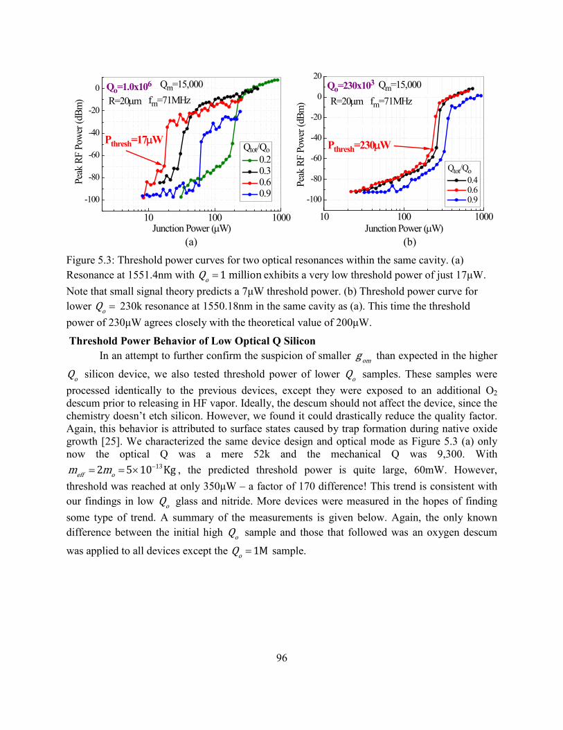
96
10 100 1000
-100
-80
-60
-40
-20
0 Qo=1.0x10⁶
fm=71MHz
Pthresh=17µW
R=20µmQm=15,000
Peak
RF
Powe
r (dB
m)
Junction Power (µW)
0.2 0.3 0.6 0.9
Qtot/Qo
10 100 1000
-100
-80
-60
-40
-20
0
20Qo=230x103
Pthresh=230µW
Qtot/Qo 0.4 0.6 0.9
Peak
RF
Powe
r (dB
m)
Junction Power (µW)
fm=71MHzR=20µmQm=15,000
(a) (b)
Figure 5.3: Threshold power curves for two optical resonances within the same cavity. (a) Resonance at 1551.4nm with 1 millionoQ = exhibits a very low threshold power of just 17μW. Note that small signal theory predicts a 7μW threshold power. (b) Threshold power curve for lower oQ = 230k resonance at 1550.18nm in the same cavity as (a). This time the threshold power of 230μW agrees closely with the theoretical value of 200μW.
Threshold Power Behavior of Low Optical Q Silicon In an attempt to further confirm the suspicion of smaller omg than expected in the higher
oQ silicon device, we also tested threshold power of lower oQ samples. These samples were processed identically to the previous devices, except they were exposed to an additional O2 descum prior to releasing in HF vapor. Ideally, the descum should not affect the device, since the chemistry doesn’t etch silicon. However, we found it could drastically reduce the quality factor. Again, this behavior is attributed to surface states caused by trap formation during native oxide growth [25]. We characterized the same device design and optical mode as Figure 5.3 (a) only now the optical Q was a mere 52k and the mechanical Q was 9,300. With
132 5 10 Kgeff om m −= = × , the predicted threshold power is quite large, 60mW. However, threshold was reached at only 350μW – a factor of 170 difference! This trend is consistent with our findings in low oQ glass and nitride. More devices were measured in the hopes of finding some type of trend. A summary of the measurements is given below. Again, the only known difference between the initial high oQ sample and those that followed was an oxygen descum
was applied to all devices except the 1MoQ = sample.

97
Table 5.1: Threshold power measurement results. Highlighted sample did not go through an oxygen descum prior to release. Resonances with a star are analyzed in more detail in the next section. *Indicates device is analyzed theoretically in the next section.
The 12.5r mµ= sample with 50koQ = is quite interesting since it achieves fairly low power operation without the need for a high optical Q and yet possesses high mechanical Q. The threshold power curve for it is shown below. We also characterized the sample in atmosphere rather than vacuum and the threshold power scaled appropriately with mechanical Q indicating that heat is likely not the source of threshold power discrepancy. The threshold power curve also exhibits a plateau in the carrier power fairly soon after threshold is reached. In the previous curves of Figure 5.3, this was not the case.
Radius (μm)
Qo Qmfm
(MHz)
Pthresh Measured
(W)
Pthresh Theoretical
(W)Notes
20 1M* 17μ 7μ
230k 225μ 430μ
52k* 9.3k 71 350μ 59mSeparate Device from
above17.5 114k 47μ 4.2m
77k15 170k 40μ 600μ
44k 450μ 36m
115k 14.5k 104 230μ 2mSeparate device from
above12.5 104k* 500μ 1.5m Interior optical mode
68k 260μ 5.2m50k* 250μ 13m50k 1.7k 2.5mW 130m Tested at Atm
17k127
No O2 descum15k 71
17k 87
14.5k 104

98
100 1000-100
-80
-60
-40
-20
0
Pthresh=250µW
0.48 0.62 0.74
Max
RF
Powe
r (dB
m)
Junction Power (µW)
fm=127MHzR=12.5µmQo=50x103
Qm=17,000
Qtot/Qo
Figure 5.4: Threshold power curves for a rather low oQ silicon sample with small, 12.5μm radius and high mechanical Q. The measured threshold power was 250μW while conventional OMO small signal theory predicts a value that is 50 times the measured threshold.
5.2 Free Carrier and Non-linear Effects Silicon is well known to exhibit a wealth of nonlinear phenomena [85][83] which could
play a role in the optomechanical dynamics. For instance, any effective force which causes an increase in radiation pressure as the device radius shrinks, reduces the effective damping of the system and adds to the radiation pressure force. Likewise both the index of refraction, and absorption coefficient are dependent on the free carrier number in silicon and on a small signal level these effects could add or subtract from radiation pressure. As a first attempt in explaining the lower than expected radiation pressure in low oQ silicon, we include these effects as part of the radiation pressure dynamical equations and analyze their effect on threshold power. We find that free carrier effects reduce the threshold power. If one allows for some carrier generation due to single photon absorption at the surface, the predicted threshold power matches the measured power closely.
Several other phenomena not covered here could very well have a sizable effect on threshold power. Namely, a fluctuating cavity lifetime due to the cavity expansion causing a changing in exκ . This was found to play a sizeable role in small photonic crystal cavities [86] but aren’t expected to be relevant in the larger cavities here. Another plausible cause is the photoelastic effect or strain dependent refractive index. This effect plays a prominent role in altering the static optomechanical coupling coefficient in GaAs disks [39] and was on the same order as radiation pressure in suspended silicon beams [49]. Analysis of the photoelastic magnitude requires detailed FDTD simulations because the photoelastic coefficient is a tensor. In silicon rings the photoelastic effect may cancel in part because not all parts of the ring are oscillating with the same magnitude.

99
Free carriers can alter both the index and absorption coefficient in silicon. The former is referred to as Free Carrier Index (FCI) effect while the latter is Free Carrier Absorption, FCA. Similarly, 2nd order non-linearities exist in silicon so that the refractive index and absorption are directly proportional to the electric field squared. The former effect is dubbed self-phase modulation (or Kerr effect) while the latter is called two photon absorption. Putting them together we have,
o FCI SPM
o FCA FCA
n n n nα α α α
= + += + +
(5.1)
where 3.477on = and oα are the refractive index and loss coefficient 1[ ]m − of the cold cavity.
The free carrier and self-phase modulation contribution to the refractive index are FCIn and SPMn
respectively while FCAα and TPAα are the free carrier and two-photon contribution to the loss. The free carrier and nonlinear contributions are given by [87][88],
( )0.84 3 3 18 27( , ) 8.8 10 [ ] 8.5 [ ] 10 1.73 10 ( )FCI e h e hn N N N cm N cm N t− − − = − × + × ≈ − ×
(5.2)
2
18 182
| ( )|4.5 10 4.5 10 o o
SPMg p
c a tn n I I
n Vω− −= = × = × ⋅
(5.3)
( )3 3 18 218.5 [ ] 6.0 [ ] 10 1.45 10 ( ) ( )FCA e hN cm N cm N t N tα σ− − − −= + × ≈ × = (5.4)
2
12 122
| ( )|7.25 10 7.25 10 o o
TPAg p
c a tI I
n Vω
α α − −= = × = ×
(5.5)
Where ,e hN N are the electron and hole carrier densities assumed to be equal for our material
which is very close to intrinsic. ( ) e hN t N N= = is the time varying carrier density, 2n is the
Kerr coefficient and 2α is the TPA coefficient. I is the intensity given by 2| ( )| /o rtI a tω τ=
where the round trip time, rtτ is 2 /g orn cπ and gn was defined in chapter 2. pV is the optical
modal volume. Note that in (5.2) we wrote, ( / ) ( )on(t) = n dn dN N t+ ⋅ and similar for the rest of the time varying corrections.
5.3 Threshold Power with Free Carrier and Nonlinear Optical Effects
In the presence of free carriers and the second order nonlinearities both the cavity resonant frequency and loaded quality factor must accommodate the changes.
cold FCA TPAκ κ κ κ= + + (5.6)

100
Where coldκ is the dissipation rate in the absence of pump light and includes any single photon absorption in the bulk (assumed negligible) or surface (possibly not negligible). Using (5.4), (5.5), and (2.18) gives,
( )FCA gv N tκ σ= (5.7)
2| ( )|
TPATPA
a tκτ
= (5.8)
Where 12( / )TPA g o pv Vτ α ω −≡ . The cavity resonance frequency is altered in the presence of
dispersion due to FCI and SPM. Equations (2.2) and (3.7) now become,
( ( ), ( ))( )( )
oc co n FCI n SPM
o FCI spm
con
o
cx t n t m g n g n
n n n R x
gn
ω ω
ω
= ≈ + ++ + +
→ ≡ −
(5.9)
Substituting equations (5.2) and (5.3) we get,
( )
22
27
2 22
( ( ), ( )) ( ) ( ) | ( )|
1.73 10
| ( )|
c co om N a
cN n
c o oa n
g p
x t n t g x t g N t g a t
g gdN
cg g n
n Va t
ω ωω
ω ω
−
= + + +∂
→ ≡ = − ⋅ ×
∂→ ≡ = ⋅
∂
(5.10)
It is seen that FCI imparts a change in cavity resonant frequency opposite in sign to that imparted by xδ . Although it may seem that FCI works against radiation pressure in fact the opposite is true. If x increases, the photon number is reduced and radiation pressure decreases, which then reduces the TPA carrier generation rate in the cavity causing a reduction in ( )N t and thus cω . FCI then has the same phase with a changing cavity boundary as radiation pressure and works to reinforce any changes in the cavity radius imparted by radiation pressure. Figure 5.5 summarizes the various effects and their role in either adding or substracting from the photon field (radiation pressure) as the photon field increases.

101
Figure 5.5: Small signal illustration for effects considered in silicon. An increase in cavity photons results in more free carriers through two photon absorption and a subsequent increase in photons through free carrier index (FCI). Thus FCI acts in phase with the radiation pressure force. The opposite is true for self phase modulation and free carrier absorption.
Substituting the modified detuning and cavity loss into the coupled equations for
optomechanics ((3.18) and (3.21)) with a steady input power gives,
( )
2
22
| ( )|( )
2( ) ( ) g ( ) | ( )| ( )
g
TPA
cold
om N a in ex
a tv N t
a t i g x t N t g a t a t sσ
τκ
κ
+ +
= ∆ − − − − +
(5.11)
( )2 2( ) ( ) ( ) ( ) ( ) .ex om eff m mF t g a t m t t tx x x− = + Γ + Ω (5.12)
An equation for the carrier concentration may be derived similar to a laser medium. Carriers are lost to diffusion away from the mode volume and by trap, surface, and Auger recombination. All these rates are lumped into the electron lifetime, Nτ which is generally valid for short carrier lifetimes dominated by diffusion out of the active area [88] .
' 2
2 2
( ) | ( )|N( )2
( ) | ( )| | ( )|2
TPAs cold
N p
os cold
N TPA p
tN a ttV
N N a t a tV
κκ
τ
κτ τ
= − + + Γ
−= − + + Γ
(5.13)

102
In writing the second equation, N was assumed to be the total carrier concentration while oN is the intrinsic carrier concentration. The two-photon absorption rate was cut in half since two photons are required to generate a single electron in TPA (each photon only contributes half an electron). A new term s coldκΓ , was added which accounts for the carriers that are generated at
the surface due to surface defects or trap states: sΓ is the fraction of the cold cavity loss due to single photon absorption at the surface. Being that silicon is indirect bandgap at 1550nm, bulk absorption in silicon is negligible and does not contribute carriers. To solve for the threshold power, we follow the same procedure in chapter 3. If the dynamical variables are time invariant with steady state value written as an overbar we find,
( )
2
22
2 2
2 2
| |
20 g | |
( ) | | | | 02
g
TPA
cold
om N a in ex
ex om eff m
os cold
N TPA p
av N
i g x N g a a s
F g a m
N N a aV
x
στ
κκ
κτ τ
+ + = ∆ − − − − +
− = Ω
−= − + + Γ
(5.14)
It is assumed that the phase of ins is adjusted to make a real. Next, the dynamical variables are written as the sum of a steady state and small signal component. That is,
( ) ( ), ( ) ( )N t N N t x t x x tδ δ= + → + etc. Inserting the small signal relations into (5.11)-(5.13), throwing out all 2 ,a a Nδ δ δ etc. and their permutations, and using (5.14) one arrives at,
( )( )2
2
( *)
2
1
2( ) ( *
( *) ( )
( ) ( *)
TPA
om N a g
s coldN TPA p
ex om eff m
a a av Ng x g N aa t i a a g a a a a
N a a a aN tV
F t g a a a m x
δ δσδ
τδ δ δδ δ δ δ κ
δ δ δδ κτ τ
δ δ δ δδ
++
= ∆ − + + + − +
+= − + + Γ
− + = + Γ
( )2
mx xδ+ Ω
(5.15)
Where,
22
2
| |
| |om N a
cold gTPA
g x g N g a
a v Nκ κ στ
∆ ≡ ∆ − − −
≡ + + (5.16)
Switching to the Fourier domain by integration and defining * ( ( ))*a aδ δ≡ −Ω ,

103
( )( )2
( *)
2
1
2
( ) ( *
TPA
om N a
ga a a
v N
g x g N
a
i a i a a g a a a
a δ δσδ
τ
δ δ
δ
δ δ δ δ
κ ++
− Ω Ω = ∆ − + + +
− + (5.17)
2 ( *)( ) s cold
N TPA p
N a a a ai NV
δ δ δδ κτ τ
+− Ω Ω = − + + Γ
(5.18)
( )2 2 ( ) ( *)( )ex om eff m m
m
xF g a a a m ix δδ δ δχ
δΩ − + = + − ΩΓ + Ω =Ω
−Ω (5.19)
Where ( )mχ Ω was given in equation (3.61). The latter two equations are not explicitly dependent on each other but the free carriers may impart a force or respond to an external force when mediated by the small signal photon field, aδ . Solving for ( *)a a aδ δ+ in (5.19), and inserting into (5.18) and (5.17) one can then write both aδ and Nδ in terms of xδ and exFδ .
Eliminating Nδ then gives a single equation for aδ in terms of xδ and exFδ . We get,
( ) ( ) ( )NN ext
m
N F xχ
δ χ δ δχ
Ω = Ω − Ω (5.20)
2| |
1( ) TPA
N
s cold
N
om p
a
g V i
τ
τ
κχ
+ ΓΩ ≡
− Ω
(5.21)
Substituting aδ and ( )) ** (a aδ δ Ω≡ − back into (5.19) then allows one to Solve for the small signal force in terms of displacement, aka, the effective susceptibility,
exeff
xF δδχ
=
Where,
( )
( )
1 ( ) ( )1
1 ( ) ( )
om ax axm
eff om aF aF
g a A A
g a A Aχ
χ
∗
∗
+ Ω + −Ω=
− Ω + −Ω
(5.22)
And we used,
( ) Aax aF exta x A Fδ δ δΩ = + (5.23)

104
2
2
12 2( )
2
12 2( )
2
g NaN Nax om
m m om m om TPA m
g NaaF N N
om om TPA
vigigaA igg gi
vigaA igg gi
σχχκ χ χ χ τ χ
σχχ
κ τ
≡ − + + + +
− ∆ + Ω
−≡ + + +
− ∆ + Ω
(5.24)
Note, the factor, ( )( ) ( )om ax axg a A A xδ∗Ω + −Ω is recognized as the net small signal force
acting on the boundary. The first term comes from radiation pressure while the rest of the terms may regarded as a dynamical back action force, dbaFδ similar to (3.79), that now includes equivalent forces by free carriers and non-linear optics mediated by photons. To find the threshold power one uses equation (3.67),
( ) 1
Im ( )0 (at threshold)
eff m
effm effm
χ−
ΩΓ = − =
Ω (5.25)
Formally, the cavity mode amplitude, a is swept until 0effΓ = . Due to bistability there are often two possible solutions for which we take the lower value. There are also cases where there is no solution because excessive two-photon and carrier absorption limits the maximum number of cavity photons. This is illustrated in the two plots of Figure 5.5 below. In the first plot the imaginary part of the susceptibility is graphed as a function of the cavity mode amplitude, a with the detuning parameterized. In this case, sΓ was set to 0.5 in equation (5.15) so that the cold cavity Q was assumed to be halfway limited by surface absorption. Evident in the plot is that for small detuning, the effective damping never crosses zero due to inefficient pumping of the cavity. Many photons may be placed in the mode by increasing a but the optomechanical gain is offset by other effects.

105
102 103 104-25-20-15-10-505
10152025303540
τn=10-9Γs=0.5Qm=17k
∆/κ=4.5 ∆/κ=0.45 ∆/κ=0.045 ∆/κ=0.0045
Imχ
-1 eff
Cavity mode amplitude a, (sqrt(photons))
Qo=50k
0.0 0.2 0.4 0.6 0.8 1.00.1
1
10
τn=10-11
τn=10-10
τn=10-9
P thr
esh (
mW
)
Normalized Detuning (∆/κ)
Γs=0.5 Qm=17kQo=50k
(a) (b)
Figure 5.6: (a) Imaginary part of inverse susceptibility plotted vs. cavity mode amplitude a . For some detunings, the effective damping never reaches zero. The optimum detuning is at ~0.45 which is in line with experiments. (b) Threshold power plotted vs normalized detuning for different electron lifetimes. At some detunings the threshold power is infinite so the plot was cut-off. In this case 910Nτ −= gives 350µWthreshP = at a normalized detuning of 0.45.
Because the threshold power depends on detuning and coupling, the detuning is swept while coupling is parameterized similar to how threshold is measured. In Figure 5.5 (b) the detuning is swept and threshold power determined for each detuning point. The electron lifetime is parameterized from 10ps to 1ns. For cases where the threshold power was infinite (no zero crossing in (a)), the plot was cut-off. Evidently, for the silicon device plotted in Figure 5.4, the optimal detuning is 0.45κ∆ = . Again the surface absorption Q was set to half the total Q in this case.
Finally, the threshold power was calculated for devices marked with a star in Table 5.1. An electron lifetime of 910− seconds was assumed [88]. Three fractional surface absorption Q’s
/s surf coldκ κΓ = were chosen and the results are given in the table below. The total Q was kept at the experimentally measured value. Evident in Table 5.2, is the lower threshold powers predicted in low Q devices when free carrier “FC” and non-linear “NL” are accounted for. Even if the imperfect surface is assumed to not generate any free carriers ( 0)sΓ = the predicted thresholds are smaller and may explain the discrepancy in measured and optomechanically predicted thresholds. In the 1oQ M= sample, the additions of FC and NL effects don’t appear to change the threshold power. This is due to the high optical quality factor which promotes a dominant optomechanical force.
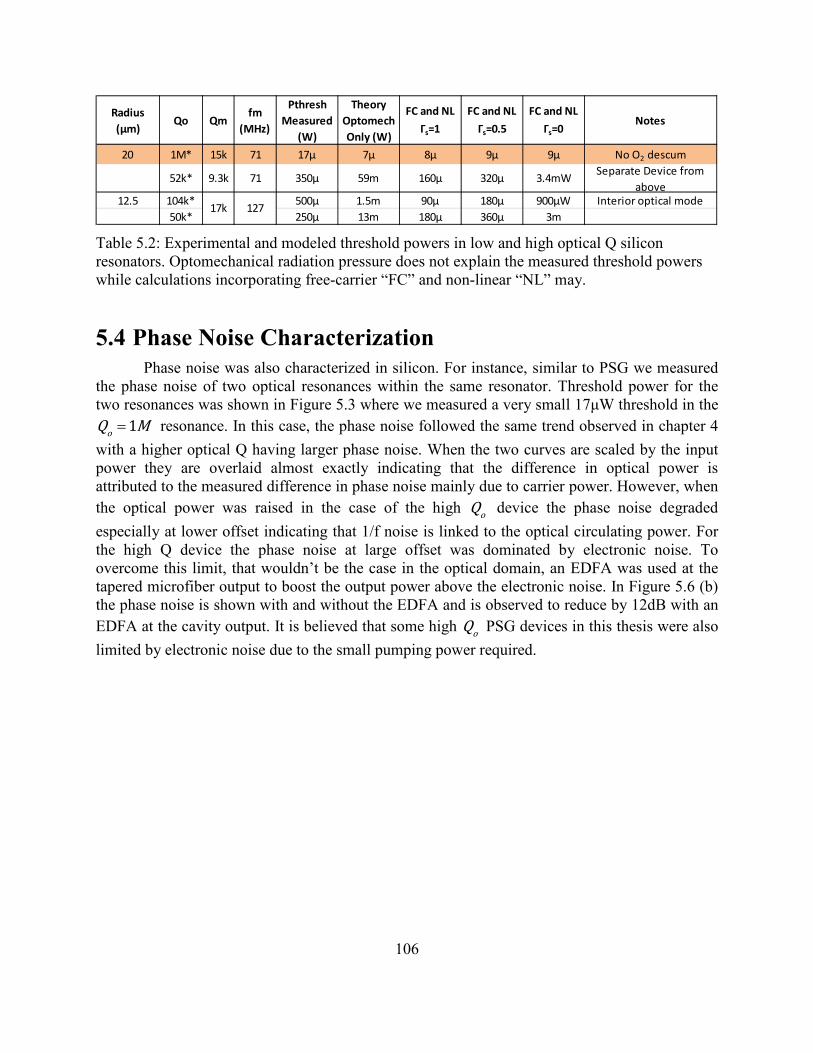
106
Table 5.2: Experimental and modeled threshold powers in low and high optical Q silicon resonators. Optomechanical radiation pressure does not explain the measured threshold powers while calculations incorporating free-carrier “FC” and non-linear “NL” may.
5.4 Phase Noise Characterization Phase noise was also characterized in silicon. For instance, similar to PSG we measured
the phase noise of two optical resonances within the same resonator. Threshold power for the two resonances was shown in Figure 5.3 where we measured a very small 17μW threshold in the
1oQ M= resonance. In this case, the phase noise followed the same trend observed in chapter 4 with a higher optical Q having larger phase noise. When the two curves are scaled by the input power they are overlaid almost exactly indicating that the difference in optical power is attributed to the measured difference in phase noise mainly due to carrier power. However, when the optical power was raised in the case of the high oQ device the phase noise degraded especially at lower offset indicating that 1/f noise is linked to the optical circulating power. For the high Q device the phase noise at large offset was dominated by electronic noise. To overcome this limit, that wouldn’t be the case in the optical domain, an EDFA was used at the tapered microfiber output to boost the output power above the electronic noise. In Figure 5.6 (b) the phase noise is shown with and without the EDFA and is observed to reduce by 12dB with an EDFA at the cavity output. It is believed that some high oQ PSG devices in this thesis were also limited by electronic noise due to the small pumping power required.
Radius (μm)
Qo Qmfm
(MHz)
Pthresh Measured
(W)
Theory Optomech Only (W)
FC and NL Γs=1
FC and NL Γs=0.5
FC and NL Γs=0
Notes
20 1M* 15k 71 17μ 7μ 8μ 9μ 9μ No O2 descum
52k* 9.3k 71 350μ 59m 160μ 320μ 3.4mW Separate Device from above
12.5 104k* 500μ 1.5m 90μ 180μ 900μW Interior optical mode50k* 250μ 13m 180μ 360μ 3m
17k 127

107
101 102 103 104 105 106 107-140
-120
-100
-80
-60
-40 Qm=15kfm=71MHz
4-SpokeRouter=20µmRinner=15.5µm
Qo=230k, Qtot/Qo=0.6Pjunction=910µW
Phas
e Noi
se (d
Bc/H
z)
Frequency Offset (Hz)
Qo=1M, Qtot/Qo=0.6Pjunction=140µW
101 102 103 104 105 106-120
-100
-80
-60
-40
-20
0 No EDFA after Tapered Fiber EDFA gain set for 600µW out
Phas
e Noi
se (d
Bc/H
z)
Frequency Offset (Hz)
12dB
(a) (b)
Figure 5.7: (a) Measured phase noise on same device from Figure 5.3. The higher optical Q resonance required lower power to achieve optimal phase noise.(b) Comparison of phase noise for oQ =1.0M resonance with and without an EDFA at the cavity output. The EDFA boosts the output noise above the electronic noise limit.
Shown below is phase noise for the 12.5μm device with threshold power measured in Figure 5.4. Recall that this sample had much lower than expected threshold power. The phase noise is also quite good and was taken with just 490μW at the coupling junction. Thus, silicon holds great promise for ultra-low power OMO’s with solid phase noise.
101 102 103 104 105 106 107
-120
-100
-80
-60
-40
-20
Phas
e Noi
se (d
Bc/H
z)
Offset Frequency (Hz)
fm=127MHzR=12.5µmQo=50x103
Qm=17,000
Pjunction
=490µW
101 102 103 104 105 106 107-140
-120
-100
-80
-60
-40
-20
Phas
e Noi
se (d
Bc/H
z)
Offset Frequency (Hz)
Normalized to 71MHz
fm=127MHz R=12.5µmPjunction=490µW
fm=71MHz, R=20µmPjunction=910µW
(a) (b)
Figure 5.8: (a) Phase noise of small R=12.5μm radius silicon sample with previously characterized threshold power of 250μW. (b) Phase noise comparison between R=12.5μm and R=20μm samples. Data is normalized to a 71MHz carrier.

108
6 Multimaterial OMO Experiments 6.1 Introduction
Mechanical Q is a win-win for phase noise and threshold power. In the quest for ever-higher mechanical Q and more device functionality, a multimaterial OMO comprising silicon nitride and polysilicon was constructed. From the previous chapters, both silicon and silicon nitride yield excellent mQ while silicon nitride has been proven to be a low 1/f noise material [14][13]. Polysilicon is known to exhibit mQ exceeding single crystalline silicon and may also be deposited with high conductivity for electrical contacts and tuning. The multimaterial OMO was designed and fabricated by Turker Beyazoglu, Tristan Rocheleau, and Karen Grutter. Some more details on the fabrication process are provided in [89].
6.2 Harmonic Locking to a Microwave Reference Since the multimaterial OMO can be made tunable via electrostatic stiffness an initial
demonstration was performed that parallels the atomic clock application. The OMO used here reaches threshold with only 1.7mW of optical power at the device input making it an attractive alternative to the microwave synthesizer currently inside of a CSAC. Similar to the proposed CSAC, we lock the ninth harmonic of the newly introduced multimaterial OMO [89] to an RF signal generator greatly improving the OMO’s long term drift while simultaneously retaining its excellent short term characteristics. In a previously reported demonstration of OMO third harmonic locking, an intensity modulator was necessary to tune the mechanical frequency through the optical spring effect [44]. Here, a voltage-controlled electrostatic stiffness common to MEMs oscillators [90] is used to tune the frequency thus forming an optomechanical voltage controlled oscillator (OMVCO) [89]. Voltage tuning eliminates the need for a separate intensity modulator and allows the optical power or detuning to be targeted for optimal phase noise, threshold power, or harmonic generation.
The recently introduced Q-boosted multimaterial OMVCO [89] shown in Figure 6.1 realizes the desired high mQ and sufficient oQ with added electrical tuning capability. Light propagates in the whispering gallery mode of a stoichiometric silicon nitride ring with intrinsic optical oQ =170,000. The mechanical quality factor of the silicon nitride ring is boosted by attaching it to a spoke-supported inner ring of polysilicon, a material with low mechanical loss. The mechanical radial breathing mode at mf =52MHz pictured in the inset of Figure 6.1(a) exhibits the lowest threshold power due to strong interaction with the radially oriented radiation pressure force and is the focus here. The largest composite mQ measured from such a device is 22,300 [89] while this work utilizes a device with mQ =17,000 at 10Torr. Voltage controlled electrostatic stiffness tuning [90] of 100ppm is attained with electrodes placed adjacent to the conductive polysilicon ring via stepper-based photolithography. Since the tuning range varies as
3/2g − where g is the gap width, further improvements in the tuning range can be made with smaller than the fitted 520nm gap. Both the electrodes and ring are electrically contacted to probe pads through a bottom polysilicon interconnect layer.
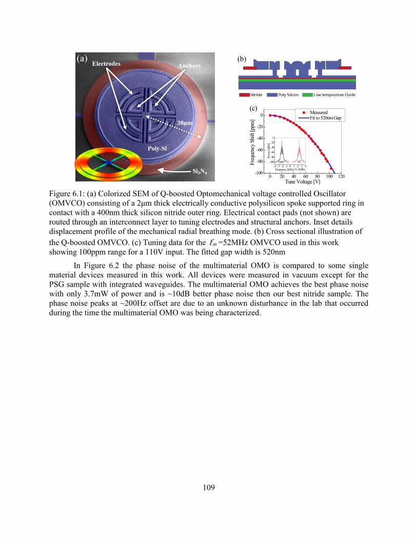
109
Figure 6.1: (a) Colorized SEM of Q-boosted Optomechanical voltage controlled Oscillator (OMVCO) consisting of a 2μm thick electrically conductive polysilicon spoke supported ring in contact with a 400nm thick silicon nitride outer ring. Electrical contact pads (not shown) are routed through an interconnect layer to tuning electrodes and structural anchors. Inset details displacement profile of the mechanical radial breathing mode. (b) Cross sectional illustration of the Q-boosted OMVCO. (c) Tuning data for the mf =52MHz OMVCO used in this work showing 100ppm range for a 110V input. The fitted gap width is 520nm
In Figure 6.2 the phase noise of the multimaterial OMO is compared to some single material devices measured in this work. All devices were measured in vacuum except for the PSG sample with integrated waveguides. The multimaterial OMO achieves the best phase noise with only 3.7mW of power and is ~10dB better phase noise then our best nitride sample. The phase noise peaks at ~200Hz offset are due to an unknown disturbance in the lab that occurred during the time the multimaterial OMO was being characterized.
0 20 40 60 80 100 120-100
-80
-60
-40
-20
0
-4 -3 -2 -1 0 1 2 3 4-100-80-60-40-20
0
100V
Pow
er [d
Bm]
Frequency [kHz]+51.9MHz
0V
Measured Fit to 520nm Gap
Freq
uenc
y Sh
ift [p
pm]
Tune Voltage [V]
(c)

110
102 103 104 105 106 107
-140
-120
-100
-80
-60
-40
-20
Vacuum
PSG integrated waveguide, 42MHz, P=270µW Silicon, 127MHz, P=490µW SiN, 74MHz, P=7.5mW Multimaterial, 52MHz, P=3.7mW
L(f)
Phas
e Noi
se, (
dBc/H
z)
Frequency Offset (Hz)
*Normalized to 52MHz*
Atmosphere
Figure 6.2: Phase noise comparison of OMO’s measured in this work. The PSG device was measured at atmosphere while the rest were taken in vacuum.
Owing to its low phase noise and voltage tunable frequency, the Q-boosted OMVCO is
an excellent candidate for locking to a microwave reference and the eventual CSAC application. At long time scales, the locked OMVCO borrows the long term stability of the lock reference. However, at short time scales the locked system will inevitably retain the frequency stability of the free running OMO since the effective lock bandwidth is limited, or intentionally kept small in the CSAC system. Thus, it is imperative that the OMO exhibits excellent short term frequency stability, typically measured as phase noise at large frequency offset. The 52MHz Q-boosted OMVCO posts phase noise of -140dBc/Hz at greater than 50kHz offset besting the specification of a 10MHz CSAC [91] and is a 20dB improvement over the previous harmonic lock demonstration [44]. As previously mentioned, voltage controlled tuning simplifies the feedback path and decouples the free running OMO performance from the locking mechanism. Measurement Setup
The Q-boosted OMVCO is harmonically locked to a low noise reference by mixing photodetected light at the cavity output with an RF signal generator set near the ninth harmonic frequency of 466MHz as shown in Figure 6.3(a). Optomechanical self-oscillation is excited by a blue-detuned narrow linewidth New Focus TLB-6700 tunable laser launched into a tapered microfiber [25, 26] controlled in the x,y,z directions by linear piezo stages. A fiber bench adjusts the polarization state of light entering the microfiber to be maximally resonant with the optical cavity. Upon evanescent coupling, light exiting the tapered microfiber travels through a

111
circulator and is coupled into a photodetector + 500Ω integrated transimpedance amplifier with 10GHz bandwidth. Imprinted on the photodetector output is the optomechanically generated frequency comb which is then amplified by 23dB. Figure 6.3(b) shows the frequency comb when pumped with 4.2mW (~2.5x threshold) at the fiber-device coupling junction where up to 14 harmonics are visible. The frequency comb then passes through a phase shifter (not shown) and mixed with a low noise SRS SG384 RF signal generator. The open loop feedback electronics include a low pass filter followed by a proportional-integral (PI) controller and a 40X high voltage amplifier. The error signal appearing at the input of the PI controller is proportional to the difference in phase between the OMVCO 9th harmonic and the signal generator. After the feedback electronics, the final control voltage is fed back to the device tuning electrodes.
Not shown in Figure 6.3 are variable optical and RF attenuators placed before and after the photodetector respectively. The attenuators are included to prevent saturation of the detector and RF amplifiers ensuring harmonics are only created through optomechanical transduction. The optical resonance is viewed in-situ on an optical spectrum analyzer which detects the output of a broadband source directed opposite the pump laser into the tapered microfiber. Air damping induced mQ degradation is minimized by housing both OMVCO and tapered microfiber in a custom vacuum chamber held at 10Torr [13]. Note that a bandpass filter is not used to isolate the desired 466MHz harmonic because in the CSAC such a filter would have to exist in the optical domain which is impractical. The described test setup is similar to a typical Pound-Drever-Hall scheme for locking a laser to an optical cavity [93] except the OMVCO acts in place of a phase modulator and the error signal is fed back to OMVCO tuning electrodes rather than the tunable laser.
100 200 300 400 500 600 700 800
-70-60-50-40-30-20-10
010
RF P
ower
[dBm
]
Frequency [MHz]
(b)
Figure 6.3: (a) Measurement setup for phase-locking the OMVCO 9th harmonic to an RF signal generator. Tunable laser light in the tapered microfiber is coupled into the device initiating self-oscillation. Light exiting the fiber is mixed with an RF signal generator, filtered and fed back to tuning electrodes. An Optical Spectrum Analyzer (OSA) simultaneously monitors transmitted light from a broadband Amplified Spontaneous Emission (ASE) source to maintain the optical coupling. (b) Photodetected OMVCO frequency comb viewed on the electrical spectrum analyzer with 4.2mW of optical power at the tapered microfiber-OMVCO coupling junction. Red outline indicates 9th harmonic used for locking.

112
6.2.1 Locking Range The OMO acts as a voltage controlled oscillator (VCO) whose open loop Nth harmonic frequency varies to first order as /(2 )N o cf NK v π∆ = where cv is the applied control voltage
and /o m cK f v= ∂ ∂ is the tuning constant for the fundamental. The expected closed-loop lock range is given by /(2 )L o df NPK K π∆ = [72] where 3200P = is the proportional gain of the PI controller multiplied by the 40X voltage amplifier. The phase detector constant, dK , is given by
/ 2d m sg oNK K v v= . Here, sgv and oNv are the voltage amplitudes at the mixer input of the signal generator and 9th harmonic which can be calculated from their separately measured RF powers of 5dBm and -28dBm respectively. The factor mK =1.2 accounts for a mixer conversion loss of 7dBm. Using these values, and an average OMVCO tune constant, 90oK π= − from Figure 6.1 (c) an expected lock range of Lf∆ =27.5kHz is calculated.
In the data that follows, the control voltage was restricted to 100V maximum to prevent pull-in, the condition where the capacitive gap is closed due to electrostatic attraction between the tuning electrodes and free-standing ring. The sample was excited with 4.2mW at the tapered microfiber-device coupling point calculated with a 99:1 splitter at the tapered microfiber input. The measured lock range for the ninth harmonic was ~28kHz in excellent agreement with the expected value of 27.5kHz. Figure 6.4(a) shows the spectrum of the ninth harmonic, and the signal generator when placed 27.5kHz below the harmonic before and after closing the loop. As expected, the OMVCO tracks the signal generator frequency within the 28kHz range. Figure 6.4(b) shows the corresponding error signal in the time domain which is initially a sinusoid at the 27.5kHz difference frequency between the two sources. Once the loop is closed, the two signal phases are gradually synced and the error signal stabilizes to ~0V upon final lock acquisition.
466.520 466.540
-125-100-75-50-25
0
466.510 466.520 466.530 466.540 466.550-125-100-75-50-25
0Generator OMVCO
9th Harmonic
27.5kHz
Unlocked Signal
(a)
Locked
RF P
ower
[dBm
]
Frequency [MHz]
0 50 100 150 200-5.0-4.0-3.0-2.0-1.00.01.02.03.04.05.0(b) OMVCO Unlocked
OMVCO Locked
Erro
r Sig
nal [
mV]
Time [µs]
Figure 6.4: (a) RF spectrum of signal generator and the OMVCO 9th harmonic at 466.5MHz before (blue) and after closing the loop (red). (b) Error signal present at the input of the PI controller as viewed on an oscilloscope. Before locking, a 27.5kHz sine wave was observed a the difference frequency between the two sources, while after lock, the error signal was maintained to ~0V by the control network.

113
Phase Noise To measure phase noise, we again used a proportional gain of P=3200 and integral gain
of I=1s-1 to produce the measured spectrums of Figure 6.5(a) taken at 52MHz. As evident in the figure, the free running OMVCO phase noise (blue) was reduced by ~85dB at 1Hz offset and ~35dB at 10Hz offset when locked (red) to the signal generator (black). At frequencies above 100Hz, the locked phase noise retained the intrinsic OMVCO spectrum emphasizing the need for low free running OMO phase noise at large offset. It is important to note that the phase noise measurement floor is set by the reference within the phase noise system. We verified, using a separate Agilent 8644B as a reference that the Q-boosted OMVCO posted better phase noise than the 8663A model for offsets between 10kHz and 1MHz (grey). In fact, the Q-boosted OMVCO reached a phase noise of -140dBc/Hz for offsets larger than 50kHz. At small frequency offsets, any free running OMO phase noise will be fundamentally limited by thermal Brownian motion, quantum backaction or input laser noise [15, 23]. These limits are circumvented by locking to the reference signal since the intrinsic phase fluctuations of the OMO are, in effect attenuated by a high pass filter further described below.
100 101 102 103 104 105 106 107
-140
-120
-100
-80
-60
-40
-20
0
Phas
e Noi
se [d
Bc/H
z]
Frequency Offset [Hz]
Unlocked OMVCO Locked OMVCO SRS Signal Generator Model P=3200, I=200
Meas Reference: 8663A
OMO: 8644B Reference
(a)
Figure 6.5: (a) Phase noise spectra of the signal generator (black) and OMVCO when unlocked (blue), and locked (red) using an Agilent 8663A phase noise measurement reference and an SRS SG384 lock reference. All curves were taken at 52MHz. Once locked, the OMVCO phase noise is suppressed by 85dB at 1Hz offset. Also shown is the OMVCO phase noise between 10kHz and 1MHz when using an Agilent 8644B phase noise measurement reference (grey) showing that within this range the OMVCO phase noise of -140dBc/Hz outperformed the 8663A reference. The modeled phase noise is shown in green. (b) Linearized model of the phase-lock electronics. The OMVCO and signal generator are modeled as perfect oscillators with time varying input phase disturbances.
Model for Closed loop Phase noise reduction
The locked OMVCO phase noise can be understood from the small signal circuit in Figure 6.5(b). Phase noise in the output signal arising from intrinsic OMVCO phase noise spectral density, noSθ , reference signal generator phase noise, nrSθ , and additive circuit voltage

114
noise, vncS , is assumed small in comparison to the carrier signal. The Nth harmonic locked OMVCO phase noise spectral density, oSθ , is a superposition of filtered input noise spectral densities [72],
2
2 21 ( ) ( ) 1 ( )
2o
o no nsg vnco
KS S H j S H j S H jNfθ θ θω ω ω
π
= − + + −
(6.1)
where all phase noise terms are evaluated ω from the carrier at 2 ofπ . vncS is the baseband power spectral density of additive circuit noise and ( )H jω is the closed-loop transfer function given by,
2
(1 )( )(1 )
o d
o d
j K K P IH jj K K P I
ωωω ω
+=
+ + (6.2)
where oK and dK were described and calculated previously. As evident from equations, (6.1)-
(6.2), the intrinsic OMVCO phase noise, noSθ undergoes a high pass filter 2
1 ( )H jω− such that the output phase noise at small offset is either greatly suppressed, or given by the signal
generator phase noise nsgSθ which experiences a low pass filter 2
( )H jω . The model curve in Figure 6.5(a) was created by inputting the measured phase noises of the OMVCO and signal generator into equation (6.1) and calculating the resulting output phase noise. An integral gain of 100s-1 was necessary to match the measured data rather than the experimental set point of 1s-1. The additional integral gain could be caused by a reduced effective loop RC time constant caused by series a capacitance. Additive circuit noise within the feedback loop was assumed negligible.
6.2.2 Long Term Stability Measurement Although the long term frequency stability of OMO’s have not previously been studied, it
is likely affected by slow drifts in temperature, pressure, and the tapered microfiber position. In addition to reduced phase noise, it is important to verify that the long term frequency drift of the locked OMVCO emulates that of the microwave reference which houses a temperature controlled crystal oscillator. To this end, the output oscillation frequency was sampled at 10Hz with an Agilent 53230A frequency counter for a10 minute duration. Figure 6.6(a) shows the OMVCO instantaneous output frequency subtracted by the average frequency, o of f− for the open loop (blue) and closed loop (red) cases. When unlocked, the OMVCO displayed a maximum frequency deviation of ~10Hz over the 10 minute span. Once locked, the frequency drift was dramatically improved and a maximum deviation of 150mHz from the average was observed matching that of the signal generator. The most common measure of frequency stability is the Allan deviation which is plotted in Figure 6.6(b) for the three oscillators in question. Once locked, the OMVCO Allan deviation was reduced by over two orders of magnitude and follows that of the signal generator. Combined with the previous phase noise data, it is evident that the composite oscillator made of the OMVCO locked to an oven-controlled crystal retains the long

115
term frequency stability of the signal generator with little to no degradation in the short term stability of the OMVCO.
0 100 200 300 400 500 600-15
-10
-5
0
5
10
15
Locked OMVCO
Freq
uenc
y De
viati
on [H
z]
Time [s]
Unlocked OMVCO
(a)
1 10 100
10-10
10-9
10-8
10-7
Alla
n De
viat
ion
Averaging Time [s]
Unlocked OMVCO Locked OMVCO Signal Generator
(b)
Figure 6.6: (a) Oscillation frequency deviation o of f− vs measurement time for the unlocked (blue) and locked (red) OMVCO. Once locked the frequency deviated by only ±150mHz from 52MHz compared to a ±10Hz deviation in the unlocked case. (b) Allan deviation curves for the three oscillators. The locked OMVCO follows the signal generator for averaging times up to 100 seconds and is more than 20dB better than the unlocked counterpart.
Optomechanical oscillators have shown great potential as sensors and as references in communications. In each application, the ultimate performance hinges on an optomechanical oscillator with a precise output frequency. Owing to its high mechanical quality factor and voltage-tunable center frequency, the Q-boosted OMVCO has emerged as an excellent candidate for such applications. We have shown that by locking the ninth harmonic of an OMVCO to a microwave reference, the phase noise at low offset is suppressed by 85dB by a loop high pass filter. This coincides with more than a 20dB reduction in the measured Allan deviation. All the while, the excellent short term, high frequency offset phase noise of the intrinsic OMVCO is retained at a level of -140dBc/Hz. The observed lock acquisition range of 28kHz can be further increased with fabrication improvements to reduce the capacitive electrode gap. Even greater improvements in Allan deviation can be made by locking an OMVCO to an atomic transition, namely a Rubidium hyperfine transition in a new chip-scale atomic clock architecture void of an electronic frequency synthesizer. This work paves the way for such an endeavor in showing that indeed by locking to a relatively high harmonic number, the long term frequency stability of the phase-locked OMVCO still emulates the reference.
6.3 High Frequency Harmonic Comb Generation One final experiment was performed on the multimaterial OMO. In chapter 3 it was
observed that obtaining a visible 3.4GHz harmonic at half the Rubidium hyperfine frequency requires a fair amount of optical power for large nonlinearities and displacement magnitude. In deriving the output power in an arbitrary harmonic in chapter 3 it was observed that each harmonic is weighted by the cavity Lorentzian evaluated at the harmonic frequency. Also, as the

116
argument, /om mg xβ = − Ω of the Bessel functions ( )nJ β increases at high amplitudes, their strength is reduced. Eventually the power in the desired harmonic saturates. In this section we experimentally verify that through RF feedback, the multimaterial OMO can serve as a high order harmonic generator.
A simple version of the setup is shown below. The Q-boosted OMVCO is driven into oscillation by the tunable laser. However, rather than running in open loop the optical output is photodetected by a 10GHz detector+500Ω TIA, amplified, phase shifted and fed back into the OMVCO through its electrical input port. In this configuration, an electrostatic force at the device center frequency and its harmonics is coherently applied during oscillation in addition to radiation pressure. Figure 6.7 (b) demonstrates harmonics well past 6GHz upon closing the feedback loop (blue) for the 52MHz OMVCO. When the feedback loop is open and the device is only driven by radiation pressure, harmonics are only visible to ~1.2GHz. In both cases, 7mW was present at the tapered microfiber-device coupling junction. This power was not optimized and its possible lower powers could generate sufficient harmonics with feedback. The 25dB RF amplifier was also not optimized and it is possible that smaller RF amplification would suffice. The opto-electromechanical setup presented below could be used, for example to excite the hyperfine transition frequency in a Rubidium CSAC. We also point out a prominent RF peak at 2.5GHz that only appears when light is injected into the device and shows up even when the OMVCO is not self-oscillating. When the laser is detuned far away from resonance, the peak no longer appears (black curve).
0 1 2 3 4 5 6 7
-90
-80
-70
-60
-50
-40
-30
-20
-10 Feedback No feedback Laser on resonance non-oscillating No feedback Laser off resonance no feedback
RF P
ower
(dBm
)
Frequency (GHz) (a) (b)
Figure 6.7: (a) Opto-electromechanical test setup for exciting a high order frequency comb in the multimaterial OMVCO. (b) Harmonics visible past 6GHz when the feedback loop was closed (blue). With no feedback harmonics were only excited up to ~1.2GHz (red). When the laser was on resonance but not at an optimal detuning for oscillation a peak at 2.5GHz was visible but then disappeared when the laser was off resonance (black).

117
In reference [66] a 6.5GHz optomechanical frequency comb was demonstrated in a photonic crystal nanobeam cavity. The quoted dropped power was 3.2mW. Since the transmission of the device was not given, it is unclear what the power was at the coupling junction. However, in the supplementary section the quoted input laser power was 23dBm which is well above our un-optimized input power of 13dBm. In the photonic crystal nanobeam, a large portion of the input optical power remains unused due to inefficient coupling from fiber to waveguide to small photonic crystal cavity. An advantage of the WGM device is the highly efficient coupling from a waveguide to the optical cavity.
7 Conclusions and Outlook In this work, a suite of optomechanical oscillators were characterized and their behavior
modeled. It was always the goal to build and test a low noise and low power optomechanical oscillator suitable for the CSAC or other integrated RF-optical oscillator system. To this end, a very low threshold 17μW, 71MHz silicon OMO was characterized exhibiting -85dBc/Hz phase noise at 1KHz offset. A 25μW, 42MHz OMO with integrated waveguides was also synthesized and the validity of PSG as a potential high optical Q material for integrated optics was verified. Optical Q’s as high as 11M were measured in wafer-scale, batch fabricated PSG, using optical and RF-optoelectronic characterization methods. Silicon nitride proved to be an excellent technology for low phase noise OMOs. A 74MHz device void of flicker noise boasted -102dBc/Hz phase noise at 1KHz offset. Finally, multimaterial OMO’s have demonstrated excellent oscillator qualities including threshold powers in the low ~1mW range, low phase noise, and tuning capability. To demonstrate the utility of such a device, the 9th harmonic of a multimaterial OMVCO was locked to a signal generator reducing its phase noise at 1Hz offset by >80dB and the long term frequency drift was stabilized. This setup could be used for improved sensing and provides a direct voltage readout of the oscillator phase. Using opto-electromechanical feedback, harmonics past 6.5GHz were excited in the OMVCO.
It is hoped that through modeling, and characterization, the path towards fabrication of low noise, low threshold OMO’s has been forged. It was shown that while high optical Q may be desired for low power applications, the phase noise of high optical Q OMOs is limited by high Brownian motion at intermediate offsets. We have observed in some devices a reduced phase noise slope at smaller frequency offsets for devices on the fringe of the sideband resolved regime. On the other hand, high mechanical quality factor was unequivocally shown to reduce phase noise and threshold power and should be the figure of merit to optimize.
Threshold power has been characterized and we have confirmed the presence of an additional force acting in sync with radiation pressure which drastically reduced observed threshold power in low 3~ 100 10oQ < × samples by as much as a factor of 170. In silicon, nonlinear optical effects including two photon absorption and self-phase modulation combined with free-carrier absorption and index were included in the small signal optomechanical coupled mode equations. It was confirmed that reduced threshold power could be explained by dissipative and dispersive free carrier effects. Provided absorption on the surface of the sample generates free carriers, the predicted threshold powers match experiments well.
The future of optomechanical oscillators is still unclear. The CSAC application has served as our guide for grading devices and the multimaterial OMVCO could fill this need. While the suggested applications could be a good fit, it is possible that the best application is yet

118
to come. For instance, optomechanics has been explored in Torque [86] , displacement [95], mass [11], and magnetic field [96] sensors. The already diverse set of optomechanical cavity structures and materials should make cavity optomechanics well poised to fill a niche. At the very least, hopefully this work helps a new researcher pick up an aspect of the field.
Bibliography [1] V. B. Braginsky, S. E. Strigin, and S. P. Vyatchanin, “Parametric oscillatory instability in
Fabry - Perot interferometer,” Phys. Lett. Sect. A Gen. At. Solid State Phys., vol. 287, no. 5–6, pp. 331–338, 2001.
[2] H. Rokhsari and T. Kippenberg, “Radiation-pressure-driven micro-mechanical oscillator,” Opt. Express, vol. 13, no. 14, pp. 5293–5301, 2005.
[3] M. Eichenfield, J. Chan, R. M. Camacho, K. J. Vahala, and O. Painter, “Optomechanical crystals.,” Nature, vol. 462, no. 7269, pp. 78–82, Nov. 2009.
[4] G. Anetsberger, O. Arcizet, Q. P. Unterreithmeier, R. Rivière, a. Schliesser, E. M. Weig, J. P. Kotthaus, and T. J. Kippenberg, “Near-field cavity optomechanics with nanomechanical oscillators,” Nat. Phys., vol. 5, no. 12, pp. 909–914, Oct. 2009.
[5] X. Sun, X. Zhang, and H. X. Tang, “High-Q silicon optomechanical microdisk resonators at gigahertz frequencies,” Appl. Phys. Lett., vol. 100, no. 17, p. 173116, 2012.
[6] L. Tian and H. Wang, “Optical wavelength conversion of quantum states with optomechanics,” Phys. Rev. A, vol. 82, no. 5, p. 053806, Nov. 2010.
[7] J. D. Teufel, T. Donner, D. Li, J. W. Harlow, M. S. Allman, K. Cicak, a J. Sirois, J. D. Whittaker, K. W. Lehnert, and R. W. Simmonds, “Sideband cooling of micromechanical motion to the quantum ground state.,” Nature, vol. 475, no. 7356, pp. 359–363, Jul. 2011.
[8] J. Chan, T. P. M. Alegre, A. H. Safavi-Naeini, J. T. Hill, A. Krause, S. Groeblacher, M. Aspelmeyer, and O. Painter, “Laser cooling of a nanomechanical oscillator into its quantum ground state,” p. 18, Jun. 2011.
[9] C. Huang, J. Fan, R. Zhang, and L. Zhu, “Internal frequency mixing in a single optomechanical resonator,” Appl. Phys. Lett., vol. 101, no. 23, p. 231112, 2012.
[10] F. Liu and M. Hossein-Zadeh, “On the spectrum of radiation pressure driven optomechanical oscillator and its application in sensing,” Opt. Commun., vol. 294, pp. 338–343, May 2013.
[11] F. Liu and M. Hossein-Zadeh, “Mass sensing with optomechanical oscillation,” IEEE Sens. J., vol. 13, no. 1, pp. 146–147, 2013.
[12] M. Hossein-Zadeh and K. J. Vahala, “Photonic RF Down-Converter Based on Optomechanical Oscillation,” IEEE Photonics Technol. Lett., vol. 20, no. 4, pp. 234–236, 2008.
[13] T. O. Rocheleau, A. J. Grine, K. E. Grutter, R. a. Schneider, N. Quack, M. C. Wu, and C. T.-C. Nguyen, “Enhancement of mechanical Q for low phase noise optomechanical oscillators,” in 2013 IEEE 26th International Conference on Micro Electro Mechanical Systems (MEMS), 2013, pp. 118–121.

119
[14] S. Sridaran and S. A. Bhave, “A Silicon Nitride Optomechanical Oscillator with Zero Flicker Noise,” in Micro Electro Mechanical Systems (MEMS), 2012 IEEE 25th International Conference on, 2012, no. February, pp. 19–22.
[15] K. E. Grutter, A. M. Yeh, A. Grine, and M. C. Wu, “An Integrated , Silica-Based , MEMS-Actuated , Tunable- Bandwidth Optical Filter with Low Minimum Bandwidth,” in Conference on Lasers and Electro-Optics, 2013, 2013, pp. 7–8.
[16] V. S. Ilchenko, J. Byrd, A. a. Savchenkov, A. B. Matsko, D. Seidel, and L. Maleki, “Miniature oscillators based on optical whispering gallery mode resonators,” in 2008 IEEE International Frequency Control Symposium, FCS, 2008, pp. 305–308.
[17] M. R. Watts, D. C. Trotter, R. W. Young, and A. L. Lentine, “Ultralow power silicon microdisk modulators and switches,” in 2008 5th International Conference on Group IV Photonics, GFP, 2008, vol. 2, no. ll, pp. 4–6.
[18] S. M. Spillane, T. J. Kippenberg, and K. J. Vahala, “Ultrahigh- Q toroidal microresonators for cavity quantum electrodynamics,” Phys. Rev. A, vol. 71, no. 1, pp. 1–10, 2005.
[19] P. Del’Haye, T. Herr, E. Gavartin, M. L. Gorodetsky, R. Holzwarth, and T. J. Kippenberg, “Octave spanning tunable frequency comb from a microresonator,” Phys. Rev. Lett., vol. 107, no. 6, p. 063901, Aug. 2011.
[20] H. Rokhsari, T. J. Kippenberg, T. Carmon, and K. J. Vahala, “Theoretical and experimental study of radiation pressure-induced mechanical oscillations (parametric instability) in optical microcavities,” IEEE J. Sel. Top. Quantum Electron., vol. 12, no. 1, pp. 96–107, 2006.
[21] K. E. Grutter, “Optical Whispering-Gallery Mode Resonators for Applications in Optical Communication and Frequency Control,” University of California, Berkeley, 2013.
[22] J. Yao, “Tunable Optical Microresonators with Micro-Electro- Mechanical-System (MEMS) Integration,” University of California, Berkeley, 2007.
[23] M. Oxborrow, “How to simulate the whispering-gallery-modes of dielectric microresonators in FEMLAB/COMSOL,” Laser Reson. Beam Control IX, vol. 6452, no. 0, pp. J4520–J4520, 2007.
[24] K. Srinivasan, M. Borselli, O. Painter, A. Stintz, and S. Krishna, “Cavity Q , mode volume , and lasing threshold in small diameter AlGaAs microdisks with embedded quantum dots,” Opt. Express, vol. 14, no. 3, pp. 1094–1105, 2006.
[25] M. Borselli, T. J. Johnson, and O. Painter, “Measuring the role of surface chemistry in silicon microphotonics,” Appl. Phys. Lett., vol. 88, no. 13, p. 131114, 2006.
[26] M. L. Gorodetsky, a a Savchenkov, and V. S. Ilchenko, “Ultimate Q of optical microsphere resonators.,” Opt. Lett., vol. 21, no. 7, pp. 453–5, Apr. 1996.
[27] H. A. Haus, Waves and Fields in Optoelectronics. New Jersey: Prentice Hall, 1983, p. 402.
[28] A. Schliesser and T. J. Kippenberg, “Chapter 5 – Cavity Optomechanics with Whispering-Gallery Mode Optical Micro-Resonators,” in Advances In Atomic, Molecular, and Optical Physics, vol. 58, 2010, pp. 207–323.
[29] X. Zhang and A. M. Armani, “Silica microtoroid resonator sensor with monolithically integrated waveguides.,” Opt. Express, vol. 21, no. 20, pp. 23592–603, Oct. 2013.
[30] H. Lee, T. Chen, J. Li, K. Y. Yang, S. Jeon, O. Painter, and K. J. Vahala, “Chemically etched ultrahigh-Q wedge-resonator on a silicon chip,” Nat. Photonics, vol. 6, no. 6, pp. 369–373, May 2012.

120
[31] T. Carmon, L. Yang, and K. J. Vahala, “Dynamical thermal behavior and thermal self- stability of microcavities,” vol. 12, no. 20, pp. 654–656, 2004.
[32] I. Grudinin, V. Ilchenko, and L. Maleki, “Ultrahigh optical Q factors of crystalline resonators in the linear regime,” Phys. Rev. A, vol. 74, no. 6, p. 063806, Dec. 2006.
[33] T. J. A. Kippenberg, “Nonlinear Optics in Ultra-high-Q Whispering-Gallery Optical Microcavities,” California Institute of Technology, 2004.
[34] G. C. Bjorklund, M. D. Levenson, W. Lenth, and C. Ortiz, “Frequency modulation (FM) spectroscopy,” Appl. Phys. B Photophysics Laser Chem., vol. 32, no. 3, pp. 145–152, 1983.
[35] P.-H. Merrer, K. Saleh, O. Llopis, S. Berneschi, F. Cosi, and G. Nunzi Conti, “Characterization technique of optical whispering gallery mode resonators in the microwave frequency domain for optoelectronic oscillators,” Appl. Opt., vol. 51, no. 20, p. 4742, 2012.
[36] L. Collot and Et Al., “Very High- Q Whispering-Gallery Mode Resonances Observed on Fused Silica Microspheres,” EPL (Europhysics Lett., vol. 23, no. 5, p. 327, 1993.
[37] V. Giovannetti and D. Vitali, “Phase-noise measurement in a cavity with a movable mirror undergoing quantum Brownian motion,” Phys. Rev. A - At. Mol. Opt. Phys., vol. 63, no. 2, pp. 1–8, Jan. 2001.
[38] D. K. Armani, T. J. Kippenberg, S. M. Spillane, and K. J. Vahala, “Ultra-high-Q toroid microcavity on a chip.,” Nature, vol. 421, no. 6926, pp. 925–928, 2003.
[39] C. Baker, W. Hease, D.-T. Nguyen, A. Andronico, S. Ducci, G. Leo, and I. Favero, “Photoelastic coupling in gallium arsenide optomechanical disk resonators.,” Opt. Express, vol. 22, no. 12, pp. 14072–86, Jun. 2014.
[40] M. L. Gorodetsky, a Schliesser, G. Anetsberger, S. Deleglise, and T. J. Kippenberg, “Determination of the vacuum optomechanical coupling rate using frequency noise calibration.,” Opt. Express, vol. 18, no. 22, pp. 23236–23246, Sep. 2010.
[41] S. Johnson, M. Ibanescu, M. Skorobogatiy, O. Weisberg, J. Joannopoulos, and Y. Fink, “Perturbation theory for Maxwell’s equations with shifting material boundaries,” Phys. Rev. E, vol. 65, no. 6, p. 066611, Jun. 2002.
[42] L. Ding, C. Baker, P. Senellart, A. Lemaitre, S. Ducci, G. Leo, and I. Favero, “High frequency GaAs nano-optomechanical disk resonator,” Phys. Rev. Lett., vol. 105, no. 26, p. 263903, Dec. 2010.
[43] L. Ding, C. Baker, P. Senellart, a. Lemaitre, S. Ducci, G. Leo, and I. Favero, “Wavelength-sized GaAs optomechanical resonators with gigahertz frequency,” Appl. Phys. Lett., vol. 98, no. 11, p. 113108, 2011.
[44] J. Zheng, Y. Li, N. Goldberg, M. McDonald, X. Luan, A. Hati, M. Lu, S. Strauf, T. Zelevinsky, D. a. Howe, and C. Wei Wong, “Feedback and harmonic locking of slot-type optomechanical oscillators to external low-noise reference clocks,” Appl. Phys. Lett., vol. 102, no. 14, p. 141117, 2013.
[45] F. Liu and M. Hossein-Zadeh, “Characterization of optomechanical rf frequency mixing/down-conversion and its application in photonic rf receivers,” J. Light. Technol., vol. 32, no. 2, pp. 309–317, 2014.
[46] A. Schliesser, R. Riviere, G. Anetsberger, O. Arcizet, and T. J. Kippenberg, “Resolved-sideband laser cooling of a micro-mechanical oscillator,” Nat. Phys., vol. 4, no. 5, pp. 415–419, Apr. 2008.

121
[47] Agilent, “Agilent Application Note: Spectrum and Signal Analyzer Measurements and Noise,” 2011.
[48] M. Poot, K. Y. Fong, M. Bagheri, W. H. P. Pernice, and H. X. Tang, “Backaction limits on self-sustained optomechanical oscillations,” Phys. Rev. A - At. Mol. Opt. Phys., vol. 86, no. 5, p. 053826, Nov. 2012.
[49] P. T. Rakich, P. Davids, and Z. Wang, “Tailoring optical forces in waveguides through radiation pressure and electrostriction,” Opt. Express, vol. 18, no. 14, pp. 14439–14453, 2010.
[50] a. Dorsel, J. D. McCullen, P. Meystre, E. Vignes, and H. Walther, “Optical bistability and mirror confinement induced by radiation pressure,” Phys. Rev. Lett., vol. 51, no. 17, pp. 1550–1553, 1983.
[51] J. Zheng, Y. Li, N. Goldberg, M. McDonald, X. Luan, A. Hati, M. Lu, S. Strauf, T. Zelevinsky, D. a. Howe, and C. Wei Wong, “Feedback and harmonic locking of slot-type optomechanical oscillators to external low-noise reference clocks,” Appl. Phys. Lett., vol. 102, no. 14, pp. 4–5, 2013.
[52] W. C. Jiang, X. Lu, J. Zhang, and Q. Lin, “High-frequency silicon optomechanical oscillator with an ultralow threshold,” Opt. Express, vol. 20, no. 14, p. 15991, 2012.
[53] E. Rubiola, Phase Noise and Frequency Stability in Oscillators. Cambridge University Press, 2010.
[54] A. Schliesser, G. Anetsberger, R. Rivière, O. Arcizet, and T. J. Kippenberg, “High-sensitivity monitoring of micromechanical vibration using optical whispering gallery mode resonators,” New J. Phys., vol. 10, no. 9, p. 095015, Sep. 2008.
[55] K. J. Vahala, “Back-action limit of linewidth in an optomechanical oscillator,” Phys. Rev. A - At. Mol. Opt. Phys., vol. 78, no. 2, p. 023832, Aug. 2008.
[56] H. Rokhsari, M. Hossein-Zadeh, A. Hajimiri, and K. Vahala, “Brownian noise in radiation-pressure-driven micromechanical oscillators,” Appl. Phys. Lett., vol. 89, no. 26, p. 261109, 2006.
[57] T. H. Lee and A. Hajimiri, “Oscillator phase noise: A tutorial,” IEEE J. Solid-State Circuits, vol. 35, no. 3, pp. 326–335, 2000.
[58] M. Hossein-Zadeh, H. Rokhsari, A. Hajimiri, and K. Vahala, “Characterization of a radiation-pressure-driven micromechanical oscillator,” Phys. Rev. A, vol. 74, no. 2, pp. 405–408, Aug. 2006.
[59] C. Fabre, M. Pinard, S. Bourzeix, a. Heidmann, E. Giacobino, and S. Reynaud, “Quantum-noise reduction using a cavity with a movable mirror,” Phys. Rev. A, vol. 49, no. 2, pp. 1337–1343, 1994.
[60] A. A. Clerk, M. H. Devoret, S. M. Girvin, F. Marquardt, and R. J. Schoelkopf, “Introduction to quantum noise, measurement, and amplification,” Rev. Mod. Phys., vol. 82, no. 2, pp. 1155–1208, Apr. 2010.
[61] O. Arcizet, P.-F. Cohadon, T. Briant, M. Pinard, and a Heidmann, “Radiation-pressure cooling and optomechanical instability of a micromirror.,” Nature, vol. 444, no. 7115, pp. 71–74, Nov. 2006.
[62] A. J. Grine, N. Quack, K. Grutter, T. O. Rocheleau, J. Huang, C. T.-C. Nguyen, and M. C. Wu, “Wafer-scale silica optomechanical oscillators with low threshold power and low phase noise for monolithic optical frequency references,” in 2012 International Conference on Optical MEMS and Nanophotonics, 2012, vol. 5, no. c, pp. 51–52.

122
[63] S. Tallur, S. Sridaran, S. a. Bhave, and T. Carmon, “Phase noise modeling of opto-mechanical oscillators,” in 2010 IEEE International Frequency Control Symposium, FCS 2010, 2010, pp. 268–272.
[64] K. Y. Fong, M. Poot, X. Han, and H. X. Tang, “Phase noise of self-sustained optomechanical oscillators,” arXiv, pp. 1–18, Apr. 2014.
[65] F. Liu, S. Alaie, Z. Leseman, and M. Hossein-Zadeh, “Sub-pg mass sensing and measurement with an optomechanical oscillator,” Opt. Express, vol. 21, no. 17, pp. 762–768, Aug. 2013.
[66] X. Luan, Y. Huang, Y. Li, J. F. McMillan, J. Zheng, S.-W. Huang, P.-C. Hsieh, T. Gu, D. Wang, A. Hati, D. a Howe, G. Wen, M. Yu, G. Lo, D.-L. Kwong, and C. W. Wong, “An integrated low phase noise radiation-pressure-driven optomechanical oscillator chipset.,” Sci. Rep., vol. 4, p. 6842, Jan. 2014.
[67] S. Li, Y.-W. Lin, Y. Xie, Z. Ren, and C. T.-C. Nguyen, “Micromechanical ‘Hollow-Disk’ Ring Resonators,” in Proceedings of the IEEE International Conference on Micro Electro Mechanical Systems (MEMS), 2004, pp. 1–4.
[68] K. E. Grutter, A. Grine, M.-K. Kim, N. Quack, T. Rocheleau, C. T. Nguyen, and M. C. Wu, “A Platform for On-Chip Silica Optomechanical Oscillators with Integrated Waveguides,” Conf. Lasers Electro-Optics 2012, vol. 3, p. CW1M.5, 2012.
[69] K. P. Jedrzejewski, F. Martinez, J. D. Minelly, C. D. Hussey, and F. P. Payne, “Tapered-Beam Expander for Single-Mode Optical-Fibre Gap Devices,” Electron. Lett., vol. 22, no. 2, pp. 105–106, 1986.
[70] C. P. Michael, M. Borselli, T. J. Johnson, C. Chrystal, and O. Painter, “An optical fiber-taper probe for wafer-scale microphotonic device characterization,” Opt. Express, vol. 15, no. 8, pp. 686–687, 2007.
[71] E. W. Connolly, “Experiments with Toroidal Microresonators in Cavity QED,” California Institute of Technology, 2009.
[72] F. M. Gardner, Phaselock Techniques, 3rd ed. John Wiley & Sons, 2005, p. 550. [73] T. L. Naing, T. O. Rocheleau, E. Alon, and C. T.-C. Nguyen, “A 78-microwatt GSM
phase noise-compliant pierce oscillator referenced to a 61-MHz wine-glass disk resonator,” in 2013 Joint European Frequency and Time Forum & International Frequency Control Symposium (EFTF/IFC), 2013, vol. 1, no. c, pp. 562–565.
[74] M. Li, W. H. P. Pernice, C. Xiong, T. Baehr-Jones, M. Hochberg, and H. X. Tang, “Harnessing optical forces in integrated photonic circuits.,” Nature, vol. 456, no. 7221, pp. 480–484, Nov. 2008.
[75] W. H. P. Pernice, M. Li, and H. X. Tang, “Optomechanical coupling in photonic crystal supported nanomechanical waveguides.,” Opt. Express, vol. 17, no. 15, pp. 12424–12432, 2009.
[76] S. Tallur and S. a. Bhave, “A silicon electromechanical photodetector,” Nano Lett., vol. 13, no. 6, pp. 2760–2765, 2013.
[77] S. Tallur, S. Sridaran, and S. A. Bhave, “A monolithic radiation-pressure driven , low phase noise silicon nitride opto-mechanical oscillator,” vol. 19, no. 24, pp. 24522–24529, 2011.
[78] X. Sun, K. Xu, and H. X. Tang, “Monolithically integrated, ultrahigh-frequency cavity nano-optoelectromechanical system with on-chip germanium waveguide photodetector,” Opt. Lett., vol. 39, no. 8, p. 2514, 2014.

123
[79] K. E. Grutter, A. J. Grine, A. Ramier, B. Scmidt, T. Beyazoglu, T. O. Rocheleau, C. T.-C. Nguyen, and M. C. Wu, “Reflowed Phosphosilicate Glass as a Material for Free Standing High Q Optical Microdisk/Ring Resonators with Integrated Waveguides,” To be Publ.
[80] M. Tien, J. F. Bauters, M. J. R. Heck, D. T. Spencer, D. J. Blumenthal, and J. E. Bowers, “Ultra-high quality factor planar Si 3 N 4 ring resonators on Si substrates,” Opt. Express, vol. 19, no. 14, pp. 13551–13556, 2011.
[81] K. Luke, A. Dutt, C. B. Poitras, and M. Lipson, “Overcoming Si3N4 film stress limitations for high quality factor ring resonators,” Opt. Express, vol. 21, no. 19, pp. 22829–22833, Sep. 2013.
[82] M. Winger, T. D. Blasius, T. P. M. Alegre, S. Meenehan, J. Cohen, and S. Stobbe, “A chip-scale integrated cavity-electro-optomechanics platform Abstract :,” vol. 19, no. 25, pp. 550–556, 2011.
[83] J. Leuthold, C. Koos, and W. Freude, “Nonlinear silicon photonics,” Nat. Photonics, vol. 4, no. 8, pp. 535–544, Jul. 2010.
[84] S. Han, T. J. Seok, N. Quack, B.-W. Yoo, and M. C. Wu, “Monolithic 50x50 MEMS Silicon Photonic Switches with Microsecond Response Time,” in Optical Fiber Communication Conference, 2014, p. M2K.2.
[85] Q. Lin, O. J. Painter, and G. P. Agrawal, “Nonlinear optical phenomena in silicon waveguides: modeling and applications.,” Opt. Express, vol. 15, no. 25, pp. 16604–44, Dec. 2007.
[86] M. Wu, A. C. Hryciw, C. Healey, D. P. Lake, M. R. Freeman, J. P. Davis, and P. E. Barclay, “Dissipative and dispersive optomechanics in a nanocavity torque sensor,” arXiv, p. 10, Mar. 2014.
[87] R. Soref and B. Bennett, “Electrooptical effects in silicon,” IEEE J. Quantum Electron., vol. 23, no. 1, pp. 123–129, Jan. 1987.
[88] T. J. Johnson, M. Borselli, and O. Painter, “Self-induced optical modulation of the transmission through a high-Q silicon microdisk resonator.,” Opt. Express, vol. 14, no. 2, pp. 817–31, Jan. 2006.
[89] T. Beyazoglu, T. O. Rocheleau, K. E. Grutter, A. J. Grine, M. C. Wu, and C. T. Nguyen, “A multi-material Q-boosted low phase noise optomechanical oscillator,” in 2014 IEEE 27th International Conference on Micro Electro Mechanical Systems (MEMS), 2014, pp. 1193–1196.
[90] H. C. Nathanson, W. E. Newell, R. A. Wickstrom, and J. R. Davis, “The Resonant Gate Transistor,” IEEE Trans. Electron Devices, vol. 14, no. 3, pp. 117–133, 1967.
[91] “Microsemi SA.45S CSAC Datasheet.” [Online]. Available: http://www.microsemi.com/products/timing-synchronization-systems/embedded-timing-solutions/components/sa-45s-chip-scale-atomic-clock#documents.
[92] J. C. Knight, G. Cheung, F. Jacques, and T. a. Birks, “Phase-matched excitation of whispering-gallery-mode resonances by a fiber taper,” Opt. Lett., vol. 22, no. 15, p. 1129, Aug. 1997.
[93] E. D. Black, “An introduction to Pound–Drever–Hall laser frequency stabilization,” Am. J. Phys., vol. 69, no. 1, p. 79, 2001.
[94] A. Matsko, A. Savchenkov, and L. Maleki, “Stability of resonant opto-mechanical oscillators,” Opt. Express, vol. 20, no. 15, pp. 16234–16244, 2012.

124
[95] K. Srinivasan, H. Miao, M. T. Rakher, M. Davan??o, and V. Aksyuk, “Optomechanical transduction of an integrated silicon cantilever probe using a microdisk resonator,” Nano Lett., vol. 11, no. 2, pp. 791–797, 2011.
[96] S. Forstner, S. Prams, J. Knittel, E. D. van Ooijen, J. D. Swaim, G. I. Harris, a. Szorkovszky, W. P. Bowen, and H. Rubinsztein-Dunlop, “Cavity Optomechanical Magnetometer,” Phys. Rev. Lett., vol. 108, no. 12, p. 120801, Mar. 2012.
[97] G. C. Bjorklund, “Frequency-Modulation spectroscopy: a new method for measuring weak absorptions and dispersions,” Opt. Lett., vol. 5, no. 1, pp. 15–17, 1980.

125
A. S21 Response of a WGM Cavity to Intensity Modulated Light In this section, the setup below is considered. Here, the wavelength of the tunable laser is fixed outside the optical resonance (See Figure 2.8) and sent into an optical intensity modulator from EO Space. A network analyzer applies an RF sinusoid that is swept in frequency. One of the intensity modulation sidebands is then swept through the cavity photodetected and read by the network analyzer. A DC bias applied to the intensity modulator modifies its response to the modulation sideband. Common intensity modulator DC bias points used here are shown in Figure A.1(b) below.
(a) (b)
Figure A.1: Measurement setup for RF frequency modulation spectroscopy of WGM resonator. A network analyzer feeds a frequency swept RF sine wave to an intensity modulator acting on a stationary laser which is detuned off the optical resonance. The signal is swept through the cavity and read by the network analyzer. (b) Intensity modulator output power as a function of bias voltage with bias points indicated. At a fixed point in time the intensity modulator is fed a sinusoidal signal at angular frequency Ω by the network analyzer. The output field can then be assumed to consist of the optical carrier at oω and sidebands at ±Ω which is true as long as the input voltage amplitude to the modulator is small compared to Vπ . The optical transmission to an arbitrary input field can be found by combining equations (2.23) and (2.24) to give:
( )( ) ( ) (i / 2) ( ) ( ) ( )in out in out ex ins t s t s t s t s tκ κ− = ∆ − − + (A.1)
Since the output of the modulator is periodic, ( )ins t , is also periodic and since the system is linear, ( )outs t is also periodic. The output then consists of signals at real integer values of Ω each weighted by the Fourier coefficient. Assuming a Fourier series expansion of the form,

126
1( ) (n) ( ) ( )in t in t
n T
s t s e s n s t e dtT
∞− Ω Ω
=−∞
= → =∑ ∫
one can integrate (A.1) to obtain,
( ) ( )
2
( ) ( ) (i / 2) ( ) ( ) ( )
( )( ) (n) 1
( ) ( ) / 2 ( ) / 2
in out in out ex in
exout ex
in
n n n n n
n
n
in s s s s s
i nsT
s i n i n
κ
κ κ
κ κκ κ
− Ω − = ∆ − − +
∆ + Ω − +→ = = = +
∆ + Ω − ∆ + Ω −
(A.2)
Which can be shown to be exactly equal to (2.35) and is also equal to (2.29) with ∆ → ∆ + Ω . Next, the output of the modulator (input to the WGM) may be written,
( )
( ) ( ) 1 exp4
bias ininmod in
o
V v tPs t s t i
Vπ
πω
+ = = +
(A.3)
Assuming the network analyzer outputs an instantaneous voltage signal of the form ( ) ( )in ov t v cos t= Ω and using equation (3.30) to expand (A.3) in terms of Bessel functions
gives,
1
( ) (0) (1) ( 1)
(0) 1 ( )4
( 1) ( )4
bias
bias
in in in in
Vi
vinin o
o
Vi
v i tinin
o
s n s s s
Ps J e
Ps i J e e
π
π
π
π
βω
βω
± Ω
≅ + + −
= +
± = −
(A.4)
With modulation index defined as,
ovVπ
β π≡
Here, (0)ins is the DC term located at the CW laser frequency while ( )ins +Ω and ( )ins −Ω are the components oscillating at Ω and −Ω with respect to the laser frequency. We used the property of the first order Bessel function, 1 1J J −= − . Only the lowest three terms were retained in the expansion which is valid for small modulation index. The output field is
( ) ( ) ( )out ins s TΩ = Ω Ω and the photodetected voltage is proportional to the output power or squared magnitude of the output power:

127
2
2
2
2
( ) ( ) ( )
( ) ( )
( 1) ( 1) (0) (0) (1) (1)
in tout o out out
n
in to in
n
i t i to in in in
P t s t s n e
T n s n e
T s e T s T s e
ω
ω
ω
∞− Ω
=−∞
∞− Ω
=−∞
Ω − Ω
= =
≅ − − + +
=
∑
∑
(A.5)
The network analyzer filters the photodetected output power and only retains the signal oscillating at t±Ω . Substituting (A.4) into (A.5) and only retaining terms with te ±Ω dependence gives,
( )2121( ) i t i tout t
P t A e A e− Ω ∗ Ω
±Ω= + (A.6)
where,
( )21 (0) (0) ( 1)s ( 1) (0) (0) (1)s (1)o in in in inA T s T T s Tω ∗ ∗ ∗ ∗≡ − − + (A.7)
Writing 21 21AiA A e ϕ−= and expanding (A.6) in terms of sines and cosines we gather,
21 21
21 21
21
( ) 2 cos( )
( ) 2
V A
V
A
S R A t
S R A
S
ϕ
ϕ
Ω = Ω +
→ Ω =
→ o =
(A.8)
where VR encompasses the voltage responsivity of the photodiode and any other subsequent electronics leading up to the network analyzer input. Now, a large red ( κ∆ − ) detuning is assumed as in Figure 2.8 such that (0) (0) 1T T ∗≈ ≈ and ( 1) 1T ∗ − ≈ . This simplifies (A.7) to,
( )* *21 (0) ( 1) (0) (1) (1) (for )o in in in inA s s s s Tω κ= − + ∆ − (A.9)
Note that the above equation is very similar to the output field obtained in [97]. Peak Bias Point When biased at the peak bias point, 0biasV = and from (A.4) one obtains,
(0) (0) /in in in os s P ω∗= = , ( 1) (1)in ins s∗ − = − . Substitution into (A.9) and (A.8) yields,
128
21( ) 2 (0) ( 1) 1 (1)
1 (1)
o V in in
p
S R s s T
A T
ω ∗Ω = − −
= −
(A.10)
Which is a peak in the RF domain and matches equation (2.36). pA is a fitting parameter. Even though large red detuning κ∆ − was assumed, an identically sized peak is obtained for large blue detuning. The FWHM of the peak may be found from (A.2) substituting 1n = , and Ω = −∆ one obtains the maximum,
21(max) 2 expS A
κκ
= (A.11)
Dividing (A.11) by 2, setting equal to (A.10) and solving for Ω gives, 32κ
±Ω = ± − ∆ so that
3FWHM κ+ −∆Ω = Ω − Ω = (A.12)
The FWHM of the 21S signal is thus related to the width of the resonance in the optical domain
by a factor of 3 . Quadrature Bias Point
At quadrature, the modulator DC bias is / 2biasV Vπ= (negative slope) and 3 / 2biasV Vπ=
(positive slope). This gives, ( )(0) / 4 1 ( )in in o os P iJω β= ± , and
1( 1) / 4 ( ) i tin in os P J eω β ± Ω± = ± where the ± pre-factor is for negative/positive slope while the
± argument in the exponent is for 1± Fourier coefficient in (A.4) . Substituting into (A.9) results in,
( )( ) ( )( )
( )( )
( ) ( )( )
21 1 1
1
2
21 1 2
1 ( ) ( ) (1) 1 ( ) ( )4
1 ( )( ) 1 ( ) 1 (1)
4 1 ( )
1 ( )( ) ( ) 1 ( ) 1 (1) (for slope)
4 1 ( )
i tino o
i t oino
o
oino
o
PA e iJ J T iJ J
iJPe J iJ T
iJ
iJPS J iJ T
J
β β β β
ββ β
β
ββ β
β
Ω
Ω
= ± ± + ±
= ± ± + ±
Ω = ± ++
(A.13)
matching equation (2.34). One can verify that in both peak and quadrature cases the largest signal is obtained when / 2ov Vπ= .

129