new hysteresis control method for three phase shunt · pdf filenew hysteresis control method...
TRANSCRIPT
New Hysteresis Control Method for Three Phase
Shunt Active Power Filter
Mohamed R. Amer, Osama A. Mahgoub, Sherif A. Zaid
Abstract—The quality of the current waveform
generated by a current controlled, voltage source shunt active
power filter depends basically on three factors: (i) The
reference signal being generated; (ii) the modulation method
used and (iii) the switching frequency of the PWM modulator.
A new adaptive hysteresis band modulation method is
proposed. In this paper, the periodical sampling constant
hysteresis band modulation method and the proposed method
are analyzed. These modulation methods are tested in
switching an active power filter based on a voltage source
topology, in a three phase three wire connections. They are
compared in terms of THD of supply current, switching losses,
and their flexibility of tuning. The simulation results
demonstrate the viability and effectiveness of the new
adaptive Hysteresis band modulation method in reducing the
ripple, losses, and THD of supply current.
Index Terms - Voltage Source Inverter (VSI), Active Power
Filter (APF), Hysteresis Modulation Technique.
I. INTRODUCTION
The performance requirements of active power filters
(APF) are hardly met by digital controls slowed down by
conversion delays and calculation times. Fast transients and
high current-harmonic content call for wide-band controls.
To obtain high accuracy and to compensate for the voltage
disturbances a high loop gain must be adopted. However, a
safe stability margin must be ensured too.
The above requirements conflict with each other. The
performance can be improved by increasing the switching
frequency. However, as in active filters, the power involved
is quite high and the available switching components do not allow too high frequencies to be adopted. Moreover, as the
switching frequency increases, the effects of the dead times
increase as well, which add to the voltages disturbances
mentioned above.
Manuscript received December 08, 2010; revised December 22, 2010.
Mohamed R. Amer is a lecturer assistant in department of Electrical
power and Machines, Faculty of Engineering, Cairo University, Egypt.
(Phone: 0020123318931; e-mail: [email protected]).
Osama A. Mahgoub is a Professor in department of Electrical power
and Machines, Faculty of Engineering, Cairo University, Egypt.
(Phone: 0020235678935; e-mail: [email protected]).
Sherif A. Zaid is a lecturer in department of Electrical power and
Machines, Faculty of Engineering, Cairo University, Egypt.
(Phone: 0020235678935; e-mail: [email protected]).
A satisfactory solution for these requirements has
proven to be the hysteresis current-control technique,
which is characterized by unconditioned stability, fast
response, and good accuracy. Although this technique is
essentially an analog one, it has been shown that the major
part of its implementation can be done by digital means,
thus obtaining several of the advantages typical of digital
solutions.
The hysteresis band is used to control the supply
current and determine the switching signals for inverters gates. When the supply current exceeds the upper band, the
comparators generate control signals in such a way to
decrease the supply current and keep it between the bands.
The basic hysteresis technique is affected by the
drawbacks of a variable switching frequency and of a
heavy interference among the phases in the case of a three-
phase system with isolated neutral. Effective methods to
eliminate these inconveniences have been introduced some
time ago and have been demonstrated to be a viable way to
obtain robust and high-performance controls. Additional
improvements were proposed [1, 2] to give the system the ability to ensure pulse-phase control to minimize the ripple
contents, similarly to the optimal pulse position produced
by the vectorial techniques [3].
In this paper, a further and substantial improvement of
the hysteresis control is proposed, which is characterized
by a very simple and robust implementation. It offers all
the advantages of the hysteresis technique.
II. THREE PHASE SHUNT APF MODEL
The shunt APF is a device that is connected parallel to
compensate the reactive power and to eliminate harmonics
from non-linear loads.
The scheme of the APF considered in this paper is
presented in Fig.1. It is a three-phase converter, where the
capacitor is the main energy storage element and the
inductors are used for the control of the filter currents by
means of the converter voltages.

Fig. 1 Fundamental building block of the active filter
Applying Kirchhoff’s laws for the currents and the
voltages at the connection point of the shunt APF leads to the
following equations in the "abc" frame [4, 5]:
1
2
3
fa
f sa n dc
fb
f sb n dc
fc
f sc n dc
diL V d V
dtdi
L V d Vdtdi
L V d Vdt
(1)
Where dnk “the switching state function” can be defined as:
1 1
2 2
3 3
2 1 1
11 2 1
31 1 2
n
n
n
d C
d C
d C
(2)
Switching function CK of the kth inverter leg (k = 1, 2, 3),
which is defined as, follows:
1, if Sk is on and Sk+3 is off
Ck =
0, if Sk is off and Sk+3 is on
III. CONTROL ALGORITHM FOR APF
In this paper, a simple Synchronous reference frame
(SRF)-based scheme is used to extract positive sequence
fundamental frequency active current from non-linear
unbalanced loads currents.
The control scheme for the proposed system is based
on the SRF based current decomposition. Figure 2 shows
the flow of various control signals and control scheme
based on the decomposed components. The control scheme
depicted in Fig.2 also incorporates the command for
maintaining the constant average DC bus voltage at the VSI.
A PI controller is used also to regulate the DC bus
voltage to its reference value and compensates for the
inverter losses. A low pass filter is used to filter the ripples
in the feedback path of the DC link voltage. The filtering of
DC voltage ensures that power transfer between the DC bus
of the inverter and supply takes place only at fundamental
frequency and not as a result of harmonic frequency. To
compensate the inverter losses and maintaining the DC bus
voltage, the demanded current is added to positive sequence fundamental frequency component of load current, as
shown in the Fig. 2.
The PWM gating pulses for the IGBTs in VSI of APF
are generated by indirect current control using hysteresis
current controller over reference supply currents (isa*, isb*,
isc*) and sensed supply currents (isa, isb, isc). The controlled
compensation current is injected such that the supply
current follows the reference current. Hence the source
current becomes close to reference currents estimated by
SRF decomposer.
Fig.2 Control scheme for APF
S1 S2 S3
Vdc Cdc
S6 S5 S4
Lf
Vsa Vsb Vsc
Ifa Ifb Ifc
Isa
Isb
Isc
ILa
ILb
ILc
Unbalanced
Nonlinear loads
Load
Currents q+
αβ abc αβ
IL+
qdc LPF
Iq+
Vdc ref
+ +
IS1R
IS+
qdc
Vdc measured
q+
αβ
LPF P
I
+
αβ
abc
-
ILoss

IV. MATLAB BASED SIMULATION
The power supply, rectifier with resistive load,
unbalanced load and APF is modeled in MATLAB using
Power System Block set. Figure 3 depicts the test bench to
estimate the performance of the APF with proposed control
scheme. The source block consists of three-phase voltage source with small impedance representing a stiff source to
gauge the performance of the APF with proposed scheme.
The set of load consists of diode rectifier and delta connected
resistive load with unequal arm. The rectifier fed load has
been modeled as diode rectifier feeding resistance, which
represents the real power consumed by the load. The
unbalance in the load current has been generated by three
phase delta connected resistive load.
The simulation results have been studied for computing
the performance of APF with two modulation methods by
analysis through THD of supply current.
The Shunt APF consists of two main parts: a) The
Inverter, b) The controller. The controller is fed with the
measurements from the main system in addition with the
inverter currents and the voltage of the DC side of the
inverter. It produces the switching scheme of the switches
(IGBT's) of the inverter. Also, it gives the signal required for
the initial charging of the capacitor in the DC side of the
inverter.
The inverter consists of three parallel modules; each consists of two IGBT’s connected in series with their anti-
parallel diodes. The DC side is a capacitor bank (C=900μF).
The capacitor bank is first charged from the main system
supply through the charging resistance (R=15) and the diodes acting as an uncontrolled rectifier bridge. After the
initial charging of the DC capacitors, when the voltage on
the capacitor reaches certain value “230V”, this resistance
is short circuiting by a contactor. Also, a line inductor is
used at the output of each module in order to smooth the
inverter current. Forward voltages of IGBT devices and diodes are 2.8V and 1V respectively. The switching times
of IGBT are 3µs. Table I presents the parameters of the
simulated system.
TABLE I
THE PARAMETERS OF THE SIMULATED SYSTEM
Total Line impedance Ls=0.733 mH, Rs=0.1Ω
Unbalanced delta connected load Rab=67Ω,Rcb=Rca=135Ω
Non-linear load(rectifier with Rdc) Rdc=20Ω
Coupling Impedance Lf=2mH, Rf =1.0Ω
Dc bus voltage 400V
Max switching frequency 12.8kHz
Hysteresis band(Hb) 0.4A
Dead time 8µs
Line frequency 50Hz
Mains voltage per phase 100V
It must be noted that there is a delay time must be
considered in the simulation system of APF. This time is
used by the digital control system to obtain the system
voltages and currents via transducers, to sample the currents
and voltages, and to convert the signal back to analogue
signal (driving signal).This time is set to be 15µsec.
Three-Phase Shunt Active Active Power Filter
Three phase supply
Measurements display
Unbalanced Load
Nonlinear Load
Auto transformer
a
b
c
Discrete,
Ts = 7.813e-006 s.
powergui
A
B
C
a
b
c
a b c
VabcA
B
C
a
b
c
IabcA
B
C
a
b
c
Vabc
Iabc
A
B
C
a
b
c
A
B
C
A
B
C
Ls
Vpcc_meaurements
I_load_meaurements
Iabc_supply_meaurements
Vabc_supply_meaurements
A
B
C
+
-
Fig.3 Main block of proposed control scheme with APF under MATLAB
V. PERIODICAL SAMPLING CONSTANT
HYSTERESIS BAND MODULATION METHOD
The PWM switching of VSI devices is described as follows:
If Iact > ( Iref+hb) upper switch of leg is ON and lower
switch is OFF.
If Iact < ( Iref-hb) upper switch of leg is OFF and lower
switch is ON.
Where, hb is the hysteresis band around the reference
current Iref. Number of samples over a cycle has been held
constant at 256. The loop time thus become nearly fixed at
78.125µs to realize a max possible frequency of hysteresis
controller at 12.8 kHz. A dead time of 8µs is set between
upper and lower devices of a leg of the VSI to avoid the short circuit. The hysteresis control method is simple to be
implemented, and its dynamic performance is excellent.
There are some inherent drawbacks, though [6-9]:
i. There is no intercommunication between the individual
hysteresis controllers of the three phases and hence no
strategy to generate zero voltage vectors. This increases
the switching frequency at lower modulation index.
ii. There is a tendency at lower speed to lock into limit
cycles of high-frequency switching which comprise only
nonzero voltage vectors.
iii. The current error is not strictly limited. The signal will leave the hysteresis band whenever the zero vector is
turned on while the back-emf vector has a component that
opposes the previous active switching state vector. The
maximum overshoot is ∆i.
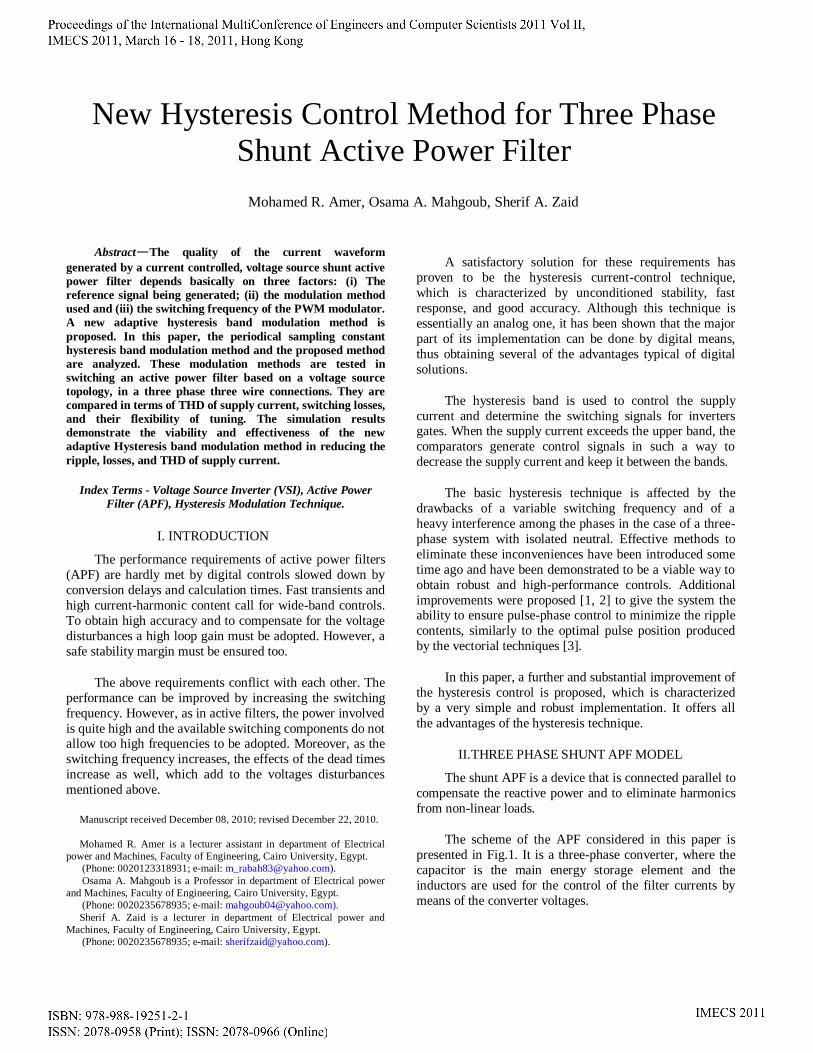
Figure 4 shows the ripple in the APF generated current.
Fig.4 Ripple in the APF generated current
Using the modeling equations of VSI as an APF
(equations 1 and 2), factors that affect the ripple in APF
generated current can be deduced.
From the previous figure, the slope of the generated APF
current (di/dt) can be calculated:
di / dt = Δi /Tsw
(3)
And the rate of change of the generated current (di/dt) is
dependent on the instantaneous supply voltage as shown in the following equation:
L di / dt = Vs – dnk Vdc
(4)
Figure 5 shows the block diagram of the hysteresis
modulation technique. This technique is called periodical
sampling constant hysteresis band. This method is very
simple to be implemented and the actual frequency is not
clearly defined but it is limited by the sampling clock.
Figure 6 shows the reference current with constant
hysteresis band. Figures7 and 8 show the simulation
results for both load and supply currents respectively for
constant hysteresis band modulation.
Fig.5 Block diagram of periodical sampling constant Hysteresis band
0.98 0.982 0.984 0.986 0.988 0.99 0.992 0.994 0.996 0.998 1-20
-15
-10
-5
0
5
10
15
20
Time (sec)
Hyste
rsis
Cu
rren
t (A
mp
)
Iref
Iref+hb
Iref-hb
Fig.6 Reference current with constant Hysteresis band
0.18 0.182 0.184 0.186 0.188 0.19 0.192 0.194 0.196 0.198 0.2-20
-15
-10
-5
0
5
10
15
20
Time (sec)
Lo
ad c
urr
ents
(Am
p)
Fig.7 Load current
0.98 0.982 0.984 0.986 0.988 0.99 0.992 0.994 0.996 0.998 1-30
-20
-10
0
10
20
30
Time (sec)
Sup
ply
curr
ent (
Am
p)
Fig.8 Supply current for constant Hysteresis band
Δi
Tsw
Iref -hb
Iref
Iref +hb
Iref
Is
Adjusting of hb
+
_
PWM
Flip-Flop
Sampling clock
D Q
CLK
I s=13.7 A, THD= 4.83 %
IL=12.6 A, THD= 19.56 %
It is noticed, in Fig. 8, the high ripple presented in
supply currents. The expressions of the ripple in the current,
equations 3and 4, show that the current ripple increases when
the switching frequency and/or the reactor value decreases.
Also, the current ripple increases when the dc bus voltage
increases. Moreover, the current ripple also affects THD especially in low currents. In previous simulation the supply
current is 13.8 Amp.
Also, in constant band periodical sampling, the
generated current does not swing symmetrically around the
reference signal: it has a biasing error.
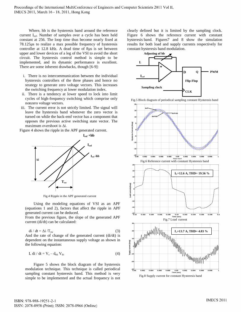
VI. NEW ADAPTIVE HYSTERESIS BAND
MODULATION METHOD
The hysteresis modulator is modified to reduce the
switching losses by applying variable frequency; to make the
generated current swing symmetrically around the reference signal with minimum possible ripple, and to adapt the
hysteresis band for any current.
The generated current can be forced to symmetrically
swing around the reference signal by making constant ripple
among the whole cycle. The ripple of the generated current is
dependent on different factors such as: instantaneous supply
voltage, dc bus voltage, coupling inductor, and the switching
time. The only controlled variable from these factors is the
switching time. The switching time can be controlled by
changing the hysteresis band.
The generated current has its maximum slope at the peak
of the supply voltage. On the other hand, the reference signal is
in phase with the supply voltage and so, its slope is minimum
value at the peak of the supply voltage. This high difference in
the rate of change between the generated current and the
reference current leads to high unsymmetrical ripple at this
instant. To reduce this ripple, the PWM signal can be forced to
track the rate of generated current to make it closer to the
reference current. As well as, the generated current has its
minimum slope and the reference signal has its maximum
slope at the minimum of the supply voltage. But (di/dt)APF is higher than (di/dt)ref at any moment. At this instant the
generated and reference currents are very close to each other.
So, PWM modulator can be forced to wait for certain
difference between the reference and the generated current. In
other words, the new modification of the modulator force the
PWM signals to turn on the IGBT devices with high switching
frequency (low switching time) at the peak of the reference
current and with low frequency (high switching time) at
minimum of the reference current.
The switching frequency of the PWM signals for periodical sampling system can be controlled by the tuning of
hysteresis band. And this achieved by making low Hysteresis
band at reference current maximum and high Hysteresis band
at reference current minimum. Figure 9 and 10 show the
block diagram of adaptive hysteresis band controller and the
relation between Hysteresis band and the reference current.
The dependence of the Hysteresis band on the rate of
change of the reference current achieves two goals; the first goal is varying the Hysteresis band around the cycle with
minimum value at peak reference current and maximum value
at minimum reference current. The second goal is self tuning
of Hysteresis band with any value of current with no need to
re-adjust the Hysteresis band. Figure 11 shows the reference
current with the new adaptive Hysteresis band.
Fig.9 Block diagram of adaptive Hysteresis band
Fig.10 Relation between adaptive Hysteresis band and reference current
0.98 0.982 0.984 0.986 0.988 0.99 0.992 0.994 0.996 0.998 1-20
-15
-10
-5
0
5
10
15
20
Time (sec)
Hys
trer
esis
Cur
rent
(Am
p)
Fig.11 Reference current with adaptive Hysteresis band
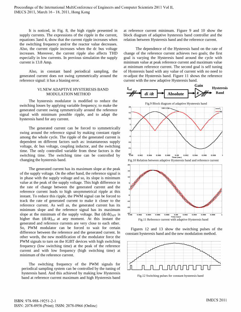
Figures 12 and 13 show the switching pulses of the
constant hysteresis band and the new modulation method.
0.94 0.941 0.942 0.943 0.944 0.945 0.946 0.947 0.948 0.949 0.95-2
0
2
4
6
8
10
12
14
16
Time (sec)
Refer
ence c
urrent
s (Amp
)
0.815 0.816 0.817 0.818 0.819 0.82 0.821 0.822 0.823 0.824 0.825-2
-1.5
-1
-0.5
0
0.5
1
1.5
2
Fig.12 Switching pulses for constant hysteresis band
di /dt
Iref Hysteresis
Band
Gain
K Absolute
0.94 0.941 0.942 0.943 0.944 0.945 0.946 0.947 0.948 0.949 0.95-2
0
2
4
6
8
10
12
14
16
Time (sec)
Refer
ence c
urrent
s (Amp
)
0.815 0.816 0.817 0.818 0.819 0.82 0.821 0.822 0.823 0.824 0.825-2
-1.5
-1
-0.5
0
0.5
1
1.5
2
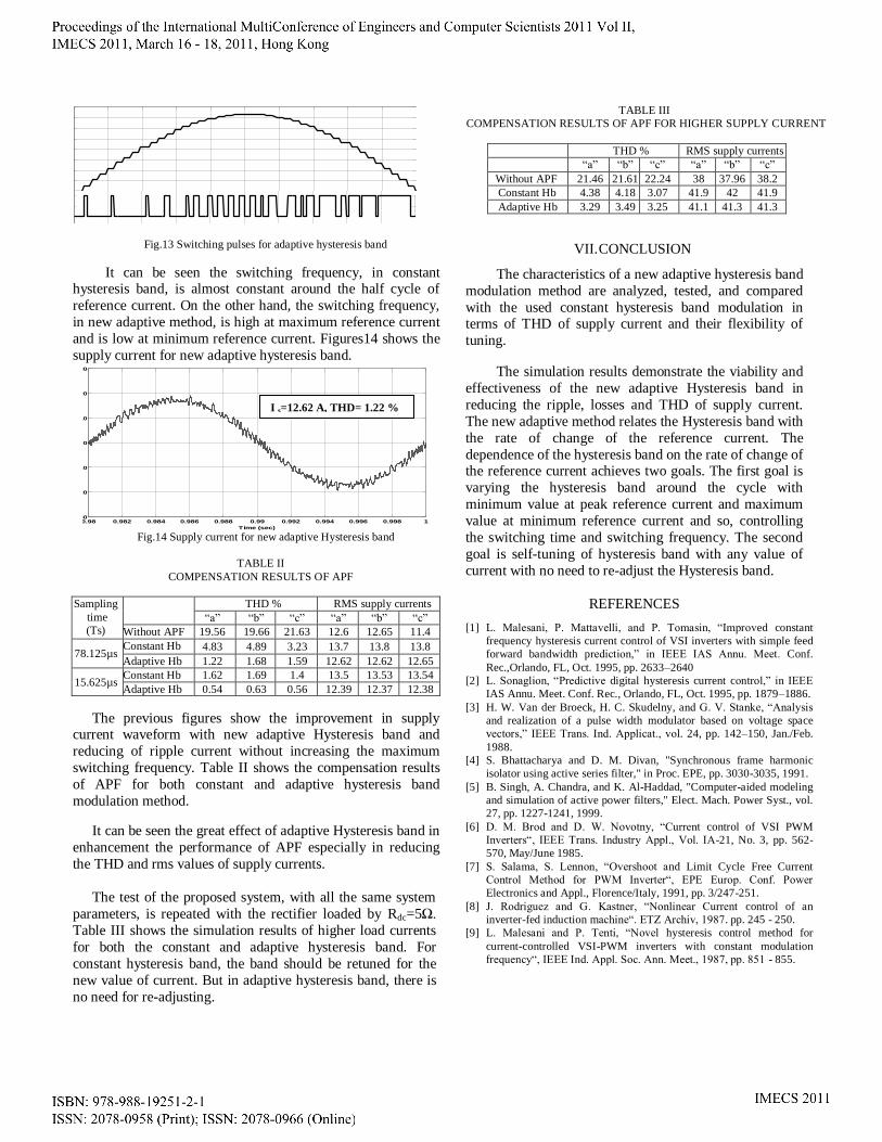
Fig.13 Switching pulses for adaptive hysteresis band
It can be seen the switching frequency, in constant hysteresis band, is almost constant around the half cycle of
reference current. On the other hand, the switching frequency,
in new adaptive method, is high at maximum reference current
and is low at minimum reference current. Figures14 shows the
supply current for new adaptive hysteresis band.
0.98 0.982 0.984 0.986 0.988 0.99 0.992 0.994 0.996 0.998 1-30
-20
-10
0
10
20
30
Time (sec)
Supp
ly c
urre
nt (A
mp)
Fig.14 Supply current for new adaptive Hysteresis band
TABLE II
COMPENSATION RESULTS OF APF
Sampling
time
(Ts)
THD % RMS supply currents
“a” “b” “c” “a” “b” “c”
Without APF 19.56 19.66 21.63 12.6 12.65 11.4
78.125µs Constant Hb 4.83 4.89 3.23 13.7 13.8 13.8
Adaptive Hb 1.22 1.68 1.59 12.62 12.62 12.65
15.625µs Constant Hb 1.62 1.69 1.4 13.5 13.53 13.54
Adaptive Hb 0.54 0.63 0.56 12.39 12.37 12.38
The previous figures show the improvement in supply current waveform with new adaptive Hysteresis band and
reducing of ripple current without increasing the maximum
switching frequency. Table II shows the compensation results
of APF for both constant and adaptive hysteresis band
modulation method.
It can be seen the great effect of adaptive Hysteresis band in
enhancement the performance of APF especially in reducing
the THD and rms values of supply currents.
The test of the proposed system, with all the same system
parameters, is repeated with the rectifier loaded by Rdc=5Ω.
Table III shows the simulation results of higher load currents
for both the constant and adaptive hysteresis band. For
constant hysteresis band, the band should be retuned for the
new value of current. But in adaptive hysteresis band, there is
no need for re-adjusting.
TABLE III
COMPENSATION RESULTS OF APF FOR HIGHER SUPPLY CURRENT
THD % RMS supply currents
“a” “b” “c” “a” “b” “c”
Without APF 21.46 21.61 22.24 38 37.96 38.2
Constant Hb 4.38 4.18 3.07 41.9 42 41.9
Adaptive Hb 3.29 3.49 3.25 41.1 41.3 41.3
VII. CONCLUSION
The characteristics of a new adaptive hysteresis band
modulation method are analyzed, tested, and compared
with the used constant hysteresis band modulation in terms of THD of supply current and their flexibility of
tuning.
The simulation results demonstrate the viability and
effectiveness of the new adaptive Hysteresis band in
reducing the ripple, losses and THD of supply current.
The new adaptive method relates the Hysteresis band with
the rate of change of the reference current. The
dependence of the hysteresis band on the rate of change of the reference current achieves two goals. The first goal is
varying the hysteresis band around the cycle with
minimum value at peak reference current and maximum
value at minimum reference current and so, controlling
the switching time and switching frequency. The second
goal is self-tuning of hysteresis band with any value of
current with no need to re-adjust the Hysteresis band.
REFERENCES
[1] L. Malesani, P. Mattavelli, and P. Tomasin, “Improved constant
frequency hysteresis current control of VSI inverters with simple feed
forward bandwidth prediction,” in IEEE IAS Annu. Meet. Conf.
Rec.,Orlando, FL, Oct. 1995, pp. 2633–2640
[2] L. Sonaglion, “Predictive digital hysteresis current control,” in IEEE
IAS Annu. Meet. Conf. Rec., Orlando, FL, Oct. 1995, pp. 1879–1886.
[3] H. W. Van der Broeck, H. C. Skudelny, and G. V. Stanke, “Analysis
and realization of a pulse width modulator based on voltage space
vectors,” IEEE Trans. Ind. Applicat., vol. 24, pp. 142–150, Jan./Feb.
1988.
[4] S. Bhattacharya and D. M. Divan, "Synchronous frame harmonic
isolator using active series filter," in Proc. EPE, pp. 3030-3035, 1991.
[5] B. Singh, A. Chandra, and K. Al-Haddad, "Computer-aided modeling
and simulation of active power filters," Elect. Mach. Power Syst., vol.
27, pp. 1227-1241, 1999.
[6] D. M. Brod and D. W. Novotny, “Current control of VSI PWM
Inverters“, IEEE Trans. Industry Appl., Vol. IA-21, No. 3, pp. 562-
570, May/June 1985.
[7] S. Salama, S. Lennon, “Overshoot and Limit Cycle Free Current
Control Method for PWM Inverter“, EPE Europ. Conf. Power
Electronics and Appl., Florence/Italy, 1991, pp. 3/247-251.
[8] J. Rodriguez and G. Kastner, “Nonlinear Current control of an
inverter-fed induction machine“. ETZ Archiv, 1987. pp. 245 - 250.
[9] L. Malesani and P. Tenti, “Novel hysteresis control method for
current-controlled VSI-PWM inverters with constant modulation
frequency“, IEEE Ind. Appl. Soc. Ann. Meet., 1987, pp. 851 - 855.
I s=12.62 A, THD= 1.22 %