hysteresis current control in three-phase voltage · pdf filehysteresis current control in...
TRANSCRIPT

Hysteresis Current Control in Three-Phase
Voltage Source Inverter
Mirjana Milosevic
Abstract
The current control methods play an important role in power electronic cir-cuits, particulary in current regulated PWM inverters which are widely appliedin ac motor drives and continuous ac power supplies where the objective is toproduce a sinusoidal ac output. The main task of the control systems in cur-rent regulated inverters is to force the current vector in the three phase loadaccording to a reference trajectory.
In this paper, two hysteresis current control methods (hexagon and squarehysteresis based controls) of three-phase voltage source inverter (VSI) have beenimplemented. Both controllers work with current components represented instationary (α, β) coordinate system.
Introduction
Three major classes of regulators have been developed over last few decades:hysteresis regulators, linear PI regulators and predictive dead-beat regulators[1]. A short review of the available current control techniques for the three-phase systems is presented in [2].
Among the various PWM technique, the hysteresis band current control isused very often because of its simplicity of implementation. Also, besides fastresponse current loop, the method does not need any knowledge of load pa-rameters. However, the current control with a fixed hysteresis band has thedisadvantage that the PWM frequency varies within a band because peak-to-peak current ripple is required to be controlled at all points of the fundamentalfrequency wave. The method of adaptive hysteresis-band current control PWMtechnique where the band can be programmed as a function of load to optimizethe PWM performance is described in [3].
The basic implementation of hysteresis current control is based on derivingthe switching signals from the comparison of the current error with a fixed toler-ance band. This control is based on the comparison of the actual phase currentwith the tolerance band around the reference current associated with that phase.On the other hand, this type of band control is negatively affected by the phasecurrent interactions which is typical in three-phase systems. This is mainly dueto the interference between the commutations of the three phases, since eachphase current not only depends on the corresponding phase voltage but is alsoaffected by the voltage of the other two phases. Depending on load conditionsswitching frequency may vary during the the fundamental period, resulting inirregular inverter operation. In [4] the authors proposed a new method that
1

minimize the effect of interference between phases while maintaining the advan-tages of the hysteresis methods by using phase-locked loop (PLL) technique toconstrain the inverter switching at a fixed predetermined frequency.
In this paper, the current control of PWM-VSI has been implemented in thestationary (α, β) reference frame. One method is based on space vector controlusing multilevel hysteresis comparators where the hysteresis band appear as ahysteresis square. The second method is based on predictive current controlwhere the three hysteresis bands form a hysteresis hexagon.
Model of the Three-Phase VSI
The power circuit of a three-phase VSI is shown in figure 1. The load modelis consisting of a sinusoidal inner voltage e and an inductance (L).
ec
eb
+
+
+
L
L
L
Sa
Sb
Sc
C
ia
ib
ic
idc
Udc
ea
+
-
Figure 1: VSI power topology
To describe inverter output voltage and the analysis of the current controlmethods the concept of a complex space vector is applied. This concept givesthe possibility to represent three phase quantities (currents or voltages) with onespace vector. Eight conduction modes of inverter are possible, i.e. the invertercan apply six nonzero voltage vectors uk (k = 1 to 6) and two zero voltage vec-tors (k = 0, 7) to the load. The state of switches in inverter legs a, b, c denotedas Sk(Sa, Sb, Sc) corresponds to each vector uk, where for Sa,b,c = 1 the upperswitch is on and for Sa,b,c = 0 the lower switch is on. The switching rules areas following: due to the DC-link capacitance the DC voltage must never be in-terrupted and the distribution of the DC-voltage Udc into the three line-to-linevoltages must not depend on the load. According to these rules, exact one ofthe upper and one of the lower switches must be closed all the time.
There are eight possible combinations of on and off switching states. Thecombinations and the corresponding phase and line-to-line voltages for eachstate are given in table 1 in terms of supplying DC voltage Udc.
If we use the transformation from three-phase (a,b,c) into stationary (α, β)coordinate system:
2

[
uαuβ
]
=
[
2
3
−1
3
−1
3
0 1√
3
−1√
3
]
uaubuc
(1)
this results in eight allowed switching states that are given in table 1 and figure 2.
State Sa Sb Sc ua/Udc ub/Udc uc/Udc uab ubc uca uα/Udc uβ/Udc
u0
0 0 0 0 0 0 0 0 0 0 0
u5
0 0 1 −1/3 −1/3 2/3 0 -1 1 −1/3 −1/√
3
u3
0 1 0 −1/3 2/3 −1/3 -1 1 0 −1/3 1/√
3u
40 1 1 −2/3 1/3 1/3 -1 0 1 −2/3 0
u1
1 0 0 2/3 −1/3 −1/3 1 0 -1 2/3 0
u6
1 0 1 1/3 −2/3 1/3 1 -1 0 1/3 −1/√
3
u2
1 1 0 1/3 1/3 −2/3 0 1 -1 1/3 1/√
3u
71 1 1 0 0 0 0 0 0 0 0
Table 1: On and Off states and corresponding outputs of a three-phase VSI
u2(110)
uref
S2
S3
S1
S4
S5
S6
u1(100)
u6(101)u5(001)
u4(011)
u3(010)
u0(000)u7(111)
a
b
1
3DC
U2
3DC
U1
3DC
U-2
3DC
U-
1
3DC
U
1
3DC
U-
Figure 2: Switching states of the VSI output voltage
3
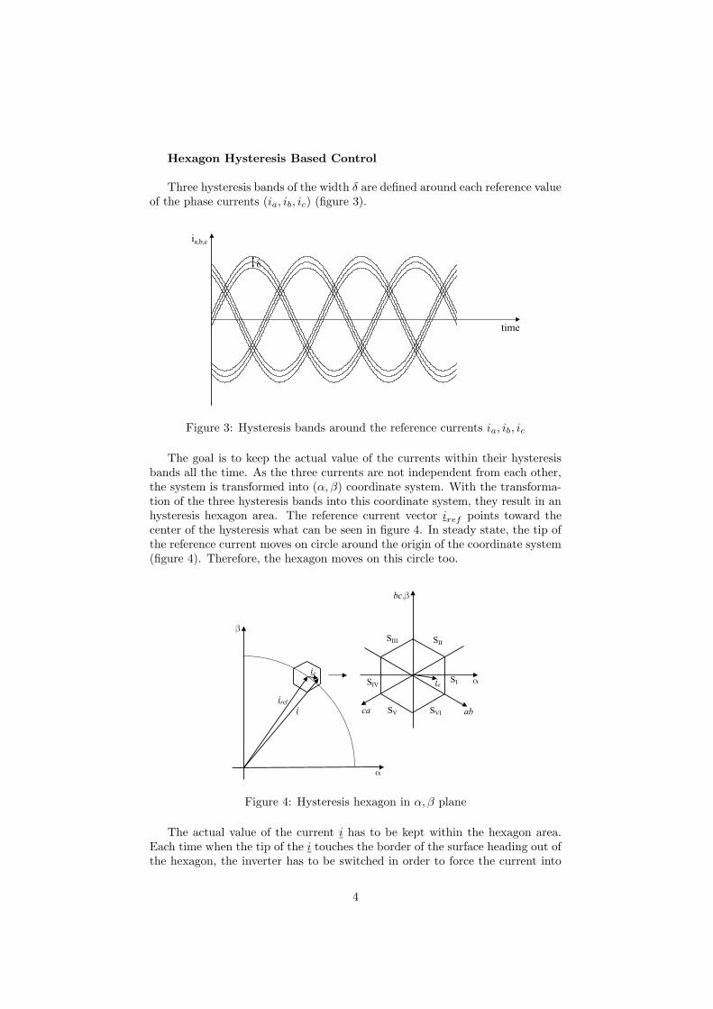
Hexagon Hysteresis Based Control
Three hysteresis bands of the width δ are defined around each reference valueof the phase currents (ia, ib, ic) (figure 3).
d
ia,b,c
time
Figure 3: Hysteresis bands around the reference currents ia, ib, ic
The goal is to keep the actual value of the currents within their hysteresisbands all the time. As the three currents are not independent from each other,the system is transformed into (α, β) coordinate system. With the transforma-tion of the three hysteresis bands into this coordinate system, they result in anhysteresis hexagon area. The reference current vector iref points toward thecenter of the hysteresis what can be seen in figure 4. In steady state, the tip ofthe reference current moves on circle around the origin of the coordinate system(figure 4). Therefore, the hexagon moves on this circle too.
iref
i
ie
a
b
bc,b
abca
aSI
SIISIII
SIV
SV SVI
ie
Figure 4: Hysteresis hexagon in α, β plane
The actual value of the current i has to be kept within the hexagon area.Each time when the tip of the i touches the border of the surface heading out ofthe hexagon, the inverter has to be switched in order to force the current into
4

the hexagon area. The current error is defined as:
ie = i− iref (2)
The error of each phase current is controlled by a two level hysteresis com-parator, which is shown in figure 5. A switching logic is necessary because ofthe coupling of three phases.
SI
SIV
SIII
SVI
SV
SII
ia,ref
ib,ref
ic,ref
ia
ib
ic
Switchinglogic
Switchesstates
d
d
d
Figure 5: Structure of hysteresis control
When the current error vector ie touches the edge of the hysteresis hexagon,the switch logic has to choose next, the most optimal switching state with re-spect to the following:
1) the current difference ie should be moved back towards the middle of thehysteresis hexagon as slowly as possible to achieve a low switching frequency;
2) if the tip of the current error ie is outside of the hexagon, it should bereturned in hexagon as fast as possible (important for dynamic processes).
In order to explain the control method the mathematical equations shouldbe introduced (figure 6).
uk
i L+
e
Figure 6: The load presentation
di
dt=
1
L(uk − e) (3)
5

According to equation 2, the current error deviation is given by:
diedt
=di
dt−
direfdt
(4)
From equations (3) and (4) we have:
diedt
=1
L(uk − uref ) (5)
where the reference voltage uref is defined by:
uref = e+ Ldirefdt
(6)
The reference voltage uref is the voltage which would allow that the actualcurrent i is identical with its reference value iref . In [5] the authors explainedwhy the decisive voltage for the current control is the sum of the inner voltageand the voltage across the inductance of the load.
The switching logic for the switches has to select the most optimal out ofeight switching states according to the mentioned criteria. For the optimalchoice of the switching state, only two pieces of information are required:
1) the sector S1, S2, ..., S6 (figure 2) of the reference voltage,
2) the sector SI , SII , ..., SV I (figure 4) in which the current error vectortouches the border of the hexagon.
For the derivation of the stationary switching table one example would bediscussed. Let reference voltage vector uref be somewhere in sector S1 (figure2). According to equation 5 the current error deviation is somewhere in one ofthe hatched areas in figure 7.
These seven areas describe direction and speed with which the current errordeviation can move.
1. If ie touches the border of hexagon in sector SI :
To get back towards the middle of the hexagon, ie must move in direction ofa negative α component. It means that vector uk−uref must have a negative αcomponent. The hatched areas A0, A3, A4 and A5 corresponding in full to this
6

u2
uref
u1
u6u5
u4
u3
u0
u7
a
bc, b
abca
u u1 ref-
A1
u u2 ref-u u3 ref-
u u4 ref-u u0- ref
u u5 ref- u u6- ref
u u7 ref-
A2A3
A4
A5 A6
A0,7
Figure 7: Corresponding areas for uk − uref
criterion are those that suit for states u0, u
3, u
4and u
5. The second criterion
for the choice of the next optimal state is the length of vector uk−uref , which isproportional to the speed of ie. The speed should be as small as possible, whichimplies that the length of vector uk − uref must be the shortest. It can be seenfrom figure 7 that state u
0is the optimal choice because vector u
0− uref has
the minimum length.
2. If ie touches the border of hexagon in sector SII :
To get back ie towards the middle of hexagon, vector uk − uref must bebelow the ab axis. Hatched areas A0, A4, A5 and A6 fulfil this condition (figure7). Vector u
0− uref has the shortest length among vectors uk − uref (k=0, 4,
5, 6). Therefore, state u0is the optimal choice.
3. If ie touches the border of hexagon in sector SIII :
To get back ie towards the middle of hexagon, vector uk − uref must bebelow ca axis (figure 7). Areas A1, A5 and A6 satisfy this condition in full andstate u
1has the shortest length of vector u
1−uref and this is the optimal choice.
4. If ie touches the border of hexagon in sector SIV :
To get back towards the middle of hexagon, vector ie must move in directionof a positive α component (figure 7). Only state u
1satisfies this condition fully
and therefore, this is the optimal choice.
7
5. If ie touches the border of hexagon in sector SV :
To get back ie towards the middle of hexagon, vector uk − uref must be be-yond ab axis. Only state u
2fulfils this condition and this is the optimal choice
(figure 7).
6. If ie touches the border of hexagon in sector SV I :
To get back ie towards the middle of hexagon, vector uk − uref must bebeyond ca axis. Areas A2, A3 and A4 (figure 7) fulfil this condition, but stateu
2has the shortest length of the corresponding vector u
2− uref and this is the
optimal choice.
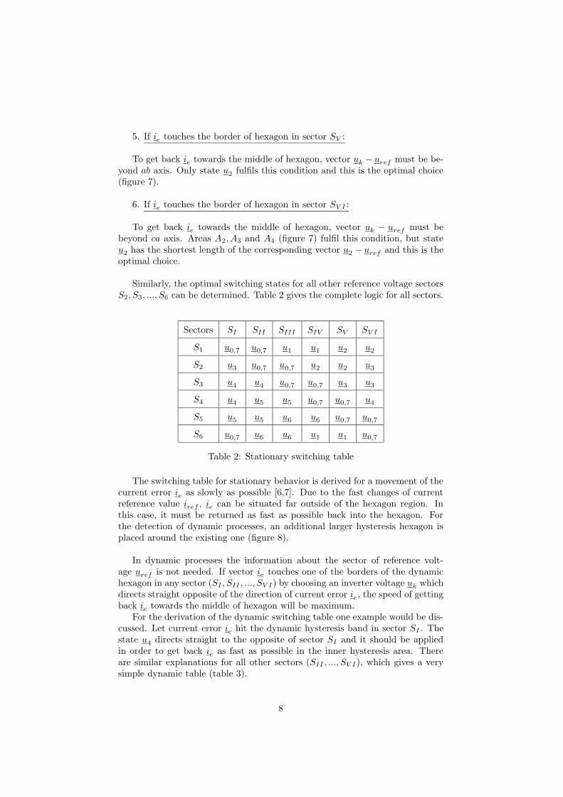
Similarly, the optimal switching states for all other reference voltage sectorsS2, S3, ..., S6 can be determined. Table 2 gives the complete logic for all sectors.
Sectors SI SII SIII SIV SV SV I
S1 u0,7 u
0,7 u1
u1
u2
u2
S2 u3
u0,7 u
0,7 u2
u2
u3
S3 u4
u4
u0,7 u
0,7 u3
u3
S4 u4
u5
u5
u0,7 u
0,7 u4
S5 u5
u5
u6
u6
u0,7 u
0,7
S6 u0,7 u
6u
6u
1u
1u
0,7
Table 2: Stationary switching table
The switching table for stationary behavior is derived for a movement of thecurrent error ie as slowly as possible [6,7]. Due to the fast changes of currentreference value iref , ie can be situated far outside of the hexagon region. Inthis case, it must be returned as fast as possible back into the hexagon. Forthe detection of dynamic processes, an additional larger hysteresis hexagon isplaced around the existing one (figure 8).
In dynamic processes the information about the sector of reference volt-age uref is not needed. If vector ie touches one of the borders of the dynamichexagon in any sector (SI , SII , ..., SV I) by choosing an inverter voltage uk whichdirects straight opposite of the direction of current error ie, the speed of gettingback ie towards the middle of hexagon will be maximum.
For the derivation of the dynamic switching table one example would be dis-cussed. Let current error ie hit the dynamic hysteresis band in sector SI . Thestate u
4directs straight to the opposite of sector SI and it should be applied
in order to get back ie as fast as possible in the inner hysteresis area. Thereare similar explanations for all other sectors (SII , ..., SV I), which gives a verysimple dynamic table (table 3).
8

SI
SIISIII
SIV
SV SVI
a
b
d
d+h
Dynamichysteresishexagon
Stationaryhysteresishexagon
Figure 8: Stationary and dynamic hysteresis hexagon
Sector SI SII SIII SIV SV SV I
Voltage u4
u5
u6
u1
u2
u3
Table 3: Dynamic switching table
Simulation Results for Hexagon Hysteresis Control
The VSI is simulated in MATLAB using PLECS. The simulation result forthe explained hexagon hysteresis control is given in figure 9 (steady state). Fromthat figure it can be seen that the vector current error stays within the hexagonarea. If we apply step change in reference current that we have that the cur-rent error goes outside of the hexagon, because the current changing causes thechange in the radius of the circle where the reference current moves on (figure4), but the hexagon tolerance surface remains the same. The simulation resultis presented in figure 10 and the step change can be seen in figure 11.
−2 −1.5 −1 −0.5 0 0.5 1 1.5 2−2
−1.5
−1
−0.5
0
0.5
1
1.5
2Hexagon Current Control (steady state)
alpha component of current error
beta
com
pone
nt o
f cur
rent
err
or
Figure 9: The current error movement in α, β plane (steady state)
9

−2 −1.5 −1 −0.5 0 0.5 1 1.5 2−2
−1.5
−1
−0.5
0
0.5
1
1.5
2Hexagon Current Control (with Iref step change)
alpha component of current error
beta
com
pone
nt o
f cur
rent
err
or
Figure 10: The current error movement in α, β plane (with step change)
0 0.002 0.004 0.006 0.008 0.01 0.012 0.014 0.016 0.018 0.02−4
−2
0
2
4Three−phase current (reference value with step change after 0.001 sec)
curr
ent
0 0.002 0.004 0.006 0.008 0.01 0.012 0.014 0.016 0.018 0.02−3
−2
−1
0
1
2
3Three−phase current (measured value)
time (sec)
curr
ent
Figure 11: Three-phase VSI current with step change in reference current after0.001 sec (hexagon control)
Square Hysteresis Based Control
The employed current control method based on square hysteresis band work-ing in (α, β) plane is show in figure 12.
Hysteresis compratorHysteresis comprator
Hysteresis compratorHysteresis comprator
Switchingtable
VSI-PWMinverter
Load
Sa
Sb
Sc
ia ref
ib ref
da
db
ia
ib
Figure 12: Block diagram of the used method for current vector control
From equation (3) it can be seen that the current vector moves in direction ofthe voltage across the load inductance, which is the difference between invertervoltage uk and inner voltage of the load e.
10
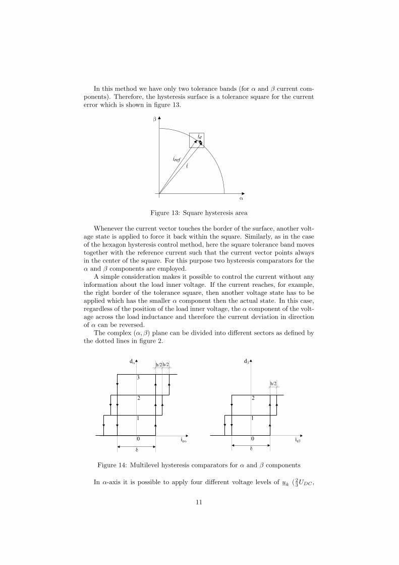
In this method we have only two tolerance bands (for α and β current com-ponents). Therefore, the hysteresis surface is a tolerance square for the currenterror which is shown in figure 13.
irefi
ie
b
a
Figure 13: Square hysteresis area
Whenever the current vector touches the border of the surface, another volt-age state is applied to force it back within the square. Similarly, as in the caseof the hexagon hysteresis control method, here the square tolerance band movestogether with the reference current such that the current vector points alwaysin the center of the square. For this purpose two hysteresis comparators for theα and β components are employed.
A simple consideration makes it possible to control the current without anyinformation about the load inner voltage. If the current reaches, for example,the right border of the tolerance square, then another voltage state has to beapplied which has the smaller α component then the actual state. In this case,regardless of the position of the load inner voltage, the α component of the volt-age across the load inductance and therefore the current deviation in directionof α can be reversed.
The complex (α, β) plane can be divided into different sectors as defined bythe dotted lines in figure 2.
da
iea0
1
2
3
db
ieb0
1
2
h/2 h/2
d d
h/2
Figure 14: Multilevel hysteresis comparators for α and β components
In α-axis it is possible to apply four different voltage levels of uk ( 2
3UDC ,
11

1
3UDC ,
−1
3UDC and −2
3UDC). In β-axis there are three voltage levels of uk (
1√
3,
0 and −1√
3). The exact selection of the appropriate voltage vector uk is deter-
mined by structure of the α and β hysteresis comparators and a correspondingswitching table (table 4). Hysteresis comparators are depicted in figure 14,where because of the simplicity hysteresis levels are denotes as 0, 1, 2 and 3.For α comparator, level 0 corresponds to level −2
3UDC , 1 to
−1
3UDC , 2 to
1
3UDC
and 3 to 2
3UDC . For β comparator level 0 corresponds to level −1
√
3, level 1 to 0
and level 2 to 1√
3.
The control scheme of this method uses one four level hysteresis comparatorfor the α component and three level hysteresis comparator for the β componentof the current vector error.
Digital outputs of the comparators (dα, dβ) select the state of the inverterswitches Sa, Sb, Sc using the switching table:
α,β levels 0 1 2 3
0 u5
u5
u6
u6
1 u4
u0,7 u
0,7 u1
2 u3
u3
u2
u2
Table 4: Switch logic table for square hysteresis control
The practical implementation of three-level hysteresis comparator is givenin figure 15. The implementation of four-level comparator is very similar.
d+
1
0
d
h/2
1
0
d
h
1
0
d
Figure 15: Practical implementation of multilevel hysteresis comparator
12

Simulation Results for Square Hysteresis Control
The VSI is simulated in MATLAB using PLECS. The simulation result forthe explained square hysteresis control is given in figure 16. It can be seen thatthe current error vector is in the square area (steady state). The simulationresult for the step change in reference current is given in figure 17. It can beseen that the current error vector goes outside of the square (similarly as forhexagon control) due to the step change in reference current because the cur-rent changing causes the change in the radius of the circle where the referencecurrent moves on (figure 13) but the square tolerance surface remains the same.
−2 −1.5 −1 −0.5 0 0.5 1 1.5 2−2
−1.5
−1
−0.5
0
0.5
1
1.5
2Square Current Control (steady state)
alpha component of current error
beta
com
pone
nt o
f cur
rent
err
or
Figure 16: The current error movement in α, β plane
−2 −1.5 −1 −0.5 0 0.5 1 1.5 2−2
−1.5
−1
−0.5
0
0.5
1
1.5
2Square Current Control (with Iref step change)
alpha component of current error
beta
com
pone
nt o
f cur
rent
err
or
Figure 17: The current error movement in α, β plane (with step change)
13
Comments
Current regulator techniques based on the hysteresis control together withswitch logic are presented. The hysteresis hexagon control requires knowledgeof the parameters of the load, while the square method does not require that.The simulation are done for the following data: E=150V, L=1mH, Udc=400V,Iref=0A, (after t=5ms, Iref=2A). The simulation time is 10ms, δ = 0.8A,h=0.4A for both control techniques.
Averaged switching frequency is higher for square method than for hexagonmethod. The switching frequencies are different for different phase switches(even for one type of control either for square or for hexagon control). With givenparameters of the circuit, for square control, the averaged switching frequency(frequency during the simulation time) for Sa is 107kHz, for Sb is 107.5kHz andfor Sc is 100.7kHz and for hexagon control, the averaged switching frequenciesare, for Sa 94.7kHz, for Sb 94.3kHz and for Sc 81.4kHz. The hexagon methodhas smaller switching frequencies because this method is based on the rule to getback current error towards the middle of the hexagon area as slowly as possible,which is not the case for square method. Also, the switching frequencies aredifferent for different phases because when one switch changes the state (eitherfrom 0 to 1 or from 1 to 0) that does not mean that other switches are changingtheir states, too (for example, if state u
1(100) is applied after state u
2(110)
then only switch Sb has to change state from 0 to 1).
14

References
1. S. Buso, L. Malesani, P. Mattavelli, ”Comparison of Current Control Tech-
niques for Active Filter Applications”, IEEE Transaction on Industrial Elec-tronics, Vol. 45, No.5, October 1998., pp.722-729
2. M.P. Kazmierkowski, L. Malesani, ”Current control techniques for three-
phase voltage-source PWM converters: a survey”, Industrial Electronics, IEEETransactions on Industrial Electronics, Vol. 45, No. 5, Oct.1998., pp. 691 -703
3. B.K. Bose, ”An Adaptive Hysteresis-Band Current Control Technique of a
Voltage-Fed PWM Inverter for Machine Drive System”,IEEE Transactions onIndustrial Electronics, Vol. 37, No.5, October 1990., pp. 402-408
4. L. Malesani, P. Mattavelli, ”Novel Hysteresis Control Method for Current-
Controlled Voltage-Source PWM Inverters with Constant Modulation Frequency”,IEEE Transaction on Industry Applications, Vol. 26, No. 1, January/February1990., pp. 88-92
5. A. Ackva, H. Reinold, R. Olesinski, ”A Simple and Self-Adapting High-
Performance Current Scheme for Three Phase Voltage Source Inverter ” PECSToledo 1992.
6. F. Jenni, D. Wuest, ”Steuerverfahren fur selbstgefuhrte Stromrichter”
7. P. Eichenberger, M. Junger, ”Predictive Vector Control of the Stator Voltagesfor an Induction Machine Drive with Current Source Inverter”, Power Electron-ics Specialists Conference, 1997. PESC ’97 Record., 28th Annual IEEE, Vol. 2,22-27 June 1997., pp. 1295-1301
15