near east university faculty of engineeringdocs.neu.edu.tr/library/6003651426.pdf · near east...
TRANSCRIPT

NEAR EAST UNIVERSITY
Faculty of Engineering
Department of Computer Engineering
FIFO (511 X36) CONTROLLER
Graduation Project COM-400
Murad Al- Juneydi
Mr. Mehmet Kadir Ozakman
Nicosia - 2007

..
AKNOWLEDGEMENT
IN THE NAME OF ALLAH, MOST GRACIOUS, MOST MERCIFUL.
I would like to express my deepest appreciation to my god who stood beside
me all the time, who supported me in all my achievements and who has given me the
power and patience to finish my college studies successfully.
Firstly I would like to thank my parents and also to my fiance" Ayten GUL"
and pay special regards for guiding me through my studies, which are enduring these
all expenses and supporting me in all events. I am nothing without their prayers. They
also encouraged me in crises. I shall never forget their sacrifices for my education so
that I can enjoy my successful life as they are expecting.
And /feel proud to pay my special regards to my project supervisor"Mehmet
Kadir OZAKMAN". He never disappointed me in any affair. He delivered me too
much information and did his best of efforts to make me able to complete my project.
He has Devine place in my heart and I am less than the half without his help. I am
really thankful to my instructor. Not to forget to give my thanks to the NEAR EAST
UNIVERSITY education staff members for their help to take this degree and to
achieve this level.
Specially" Mr. Okan DONANGIL" who always required all students respect with
his wise and character.
At the end, we will never forget the grievous and the happy days that we spent in
Cyprus, from the University to the good friends that we have enjoyed during the 4
years with them. We would like to thank them for their kindness.

.•
ABSTRACT
VHDL (Very high speed Hardware Description Language) is a programming
language: although VHDL was not designed for writing general purpose
programs, we can write any algorithm with this language. If we are able to write
programs, we will find in VHDL features similar to those found in procedural
languages such as C or PASCAL. It derives most of its syntax and semantics from
Ada. Knowing Ada is an advantage for learning VHDL because they are familiar.
Here are some advantages and general information about the VHDL
programming language:
• VHDL is designed to fill a number of needs in the design process.
• Describes the structures and the functions of a system.
• It allows the design of a system to be simulated before being manufactured, so
that the designer can test for correctness without the expense and delay the
hardware prototyping.
• It allows the description of a system at higher level of abstraction (abstraction
defines how much detail about the design is specified in a particular
description of it) to eliminate going into the design detail.
• A synthesis tool generates the detailed design.
• Portable and could be synthesized to FPGA programmable devices.
ii

•
AKNOWLEDGEMENT
ABSTRACT
TABLE OF CONTENTS
INTRODUCTION
CHAPTER ONE: FPGA Design Flow
i
ii
iii
1.1 Hardware Description Languages
1.2 Advantages of Using HDLs to Design FPGA Devices
1.2.1 Top-Down Approach for Large Projects
1.2.2 Functional Simulation Early in the Design Flow
1.2.3 Synthesis of HDL Code to Gates
1.2.4 Early Testing of Various Design Implementations
1.2.5 Reuse of RTL Code
1.3 Designing FPGA Devices with HDLs
1.3.1 Designing FPGA Devices with VHDL
1.3.2 Designing FPGA Devices with Synthesis Tools
1.3.3 Using FPGA System Features
1.3 .4 Designing Hierarchy
1.3 .5 Specifying Speed Requirements
1.4 FPGA Design Flow
1.4.1 Design Flow
1.4.2 Entering Your Design and Selecting Hierarchy
1.4.2.1 Design Entry Recommendations
1.4.2.2 Architecture Wizard
1.4.2.3 CORE Generator
1.4.3 Functional Simulation
1.4.3 .1 Simulation Recommendations
1.4.3.2 ModelSim Simulator
1.4.4 Synthesizing and Optimizing
1.4.4.1 Creating a Compile Run Script
1
2
2
2
3
3
3
4
4
4
s s s 6
6
7
8
9
9
10
12
13
13
13
14
14
iii

•. 1.4.4.2 Synthesizing Your Design
1.4.4.3 Reading Cores
1.4.5 Setting Constraints
1.4.6 Evaluating Design Size and Performance
1.4.6.1 Estimating Device Utilization and Performance
1.4.6.2 Determining Actual Device Utilization and Pre-routed
Performance
1.4.7 Evaluating Coding Style and System Features
1.4.7.1 Modifying Your Code
1.4.7.2 Using FPGA System Features
1.4.7.3 Using Xilinx-Specific Features of Your Synthesis Tool
1.4.8 Placing and Routing
1.4.9 Timing Simulation
CHAPTER TWO: ISE GENERAL INFORMATION
& USING PROJECT NAVIGATOR 2.1 ISE General Information
2.1.1 Xilinx ISE Overview
2.1.2 Design Entry
2.1.3 Synthesis
2.1.4 Implementation
2.1.5 Verification
2.1.6 Device Configuration
2.1.7 Architecture Support
2.1.8 Operating System Support
2.2 Using Project Navigator
2.2.1. Project Navigator Overview
2.2.2 Project Navigator Main Window
2.2.3 Using the Source Window
2.2.4 Using the Processes Window
iv
14
15
16
17
17
18
21
21
21
22
22
23
24
24
24
24
24
25
25
25
26
27
27
27
28
29
30

2.2.5 Process Types
2.2.6 Process Status
2.2.7 Running Processes
2.2.8 Setting Process Properties
2.2.9 Using the Workspace
2.2.10 Using the Transcript Window
2.2.11 Using the Toolbars
CHAPTER THREE: FIFO
CONTROLLER IN VHDL
31
31
33
34
35
35
36
(511 X 36) 37
· 3 .1 Requirement
3.2 Specifications
3.2.1 FIFOs Using Virtex-II Block RAM
3.2.1.1 Synchronous FIFO Using Common Clocks
3.2.1.2 Synchronous FIFO operation
3.2.1.3 Asynchronous FIFO Using Independent Clocks
3.2.1.4 Asynchronous FIFO operation
3 .2.1.5 Conclusion
3.3 How I have Created My Project
3.3.1 Creating an HDL Source
3.3.2 Creating a VHDL Source
3.3.3 Open Codes of My FIFO (511 X 36) Design
3.4 Synthesize
3 .5 Test Bench of The Design
3.6 Simulation
3.7 Implementation
Conclusion
References
38
38
38
38
40
42
43
45
46
49
49
59
65
66
72
75
76
77
V
Introduction
I have selected the VDHL coding language to learn how to do a hardware design
using the current methods and current technology.
I have selected FIFO (511 X 36) because it is used to design many electronic
devices. Nowadays you do not just buy the parts of your PC, by using the VHDL coding
system you just can write your electronic device code by your own and by using the
implementation and synthesis tools you can apply it to your device chips. In VHDL you
do not have to think about the details of your hardware, all you must do is writing codes.
The VHDL code shown in this project implements a 511x36 FIFO in a Virtex2
device. The inputs are a Clock, a Read Enable, a Write Enable, Write Data, and a
FIFO _gsr signal as an initial reset. The outputs are Read Data, Full, Empty, and the
FIFOcount outputs, which indicate how full the FIFO is.
In this project steps of creating a new project is considered. The project consists of an
introduction, 3 chapters and a conclusion.
Chapter One represents the FPGA design flow considering the Hardware
Description Language (HDL) and the advantages of Using HDLs to design FPGA
devices, designing FPGA devices with HDLs.
Chapter Two represents ISE general information & using project navigator to
create the design.
Chapter Three describes FIFO (511 X 36) CONTROLLER in VHDL about the
requirements and specification of the design, the VHDL codes, synthesis, the test bench,
simulation and the implementation of the design.
1

CHAPTER ONE: FPGA Design Flow
1.1 Hardware Description Languages
Designers use Hardware Description Languages (HDLs) to describe the behavior
and structure of system and circuit designs. This chapter includes:
• A general overview of designing FPGA devices with HDLs
• System requirements and installation instructions for designs available from the web
• A brief description of why FPGA devices are superior to ASIC devices for your design
needs understanding FPGA architecture allows you to create HDL code that effectively
uses FPGA system features. To learn more about designing FPGA devices with HDL:
• Enroll in training classes offered by Xilinx® and by the vendors of synthesis software.
• Review the sample HDL designs in the later chapters of this Guide.
• Download design examples from Xilinx Support.
• Take advantage of the many other resources offered by Xilinx, including
documentation, tutorials, Tech Tips, service packs, a telephone hotline, and an
answers database. See "Additional Resources" in the Preface of this Guide.
1.2 Advantages of Using HDLs to Design FPGA Devices
Using HDLs to design high-density FPGA devices has the following advantages:
• "Top-Down Approach for Large Projects"
• "Functional Simulation Early in the Design Flow"
• "Synthesis of HDL Code to Gates"
• "Early Testing of Various Design Implementations"
• "Reuse of RTL Code"
2

1.2.1 Top-Down Approach for Large Projects ..
Designers use HDLs to create complex designs. The top-down approach to system
design supported by HDLs is advantageous for large projects that require many designers
working together. After they determine the overall design plan, designers can work
independently on separate sections of the code.
1.2.2 Functional Simulation Early in the Design Flow
You can verify the functionality of your design early in the design flow by
simulating the HDL description. Testing your design decisions before the design is
implemented at the RTL or gate level allows you to make any necessary changes early in
the design process.
1.2.3 Synthesis of HDL Code to Gates
You can synthesize your hardware description to target the FPGA
implementation. This step:
• Decreases design time by allowing a higher-level specification of the design rather
than specifying the design from the FPGA base elements.
• Generally reduces the number of errors that can occur during a manual translation of a
hardware description to a schematic design.
• Allows you to apply the automation techniques used by the synthesis tool (such as
machine encoding styles and automatic I/0 insertion) during the optimization of
your design to the original HDL code. This results in greater optimization and
efficiency
3

1.2.4 Early Testing of Various Design Implementations
HDLs allow you to test different implementations of your design early in the
design flow. Use the synthesis tool to perform the logic synthesis and optimization into
gates. Additionally, Xilinx FPGA devices allow you to implement your design at your
computer.
Since the synthesis time is short, you have more time to explore different architectural
possibilities at the Register Transfer Level (RTL). You can reprogram Xilinx FPGA
devices to test several implementations of your design.
1.2.5 Reuse of RTL Code
You can retarget RTL code to new FPGA architectures with a minimum ofrecoding.
1.3 Designing FPGA Devices with HDLs
If you are used to schematic design entry, you may find it difficult at first to create HDL
designs. You must make the transition from graphical concepts, such as block diagrams,
state machines, flow diagrams, and truth tables, to abstract representations of design
components. Ease this transition by not losing sight of your overall design plan as you
code in HDL. To effectively use an HDL, you must understand the:
• Syntax of the language
• Synthesis and simulator software
• Architecture of your target device
• Implementation tools
4

1.3.1 Designing FPGA Devices with VHDL
VHSIC Hardware Description Language (VHDL) is a hardware description
language for designing Integrated Circuits (ICs). It was not originally intended as an
input to synthesis, and many VHDL constructs are not supported by synthesis software.
However, the high level of abstraction of VHDL makes it easy to describe the system
level components and test benches that are not synthesized.
In addition, the various synthesis tools use different subsets of the VHDL
language. The examples in this Guide work with most commonly used FPGA synthesis
software. The coding strategies presented in the remaining chapters of this Guide can
help you create HDL descriptions that can be synthesized.
1.3.2 Designing FPGA Devices with Synthesis Tools
Most of the commonly-used FPGA synthesis tools have special optimization
algorithms for Xilinx FPGA devices. Constraints and compiling options perform
differently depending on the target device. Some commands and constraints in ASIC
synthesis tools do not apply to FPGA devices. If you use them, they may adversely
impact your results. You should understand how your synthesis tool processes designs
before you create FPGA designs. Most FPGA synthesis vendors include information in
their guides specifically for Xilinx FPGA devices.
1.3.3 Using FPGA System Features
To improve device performance, area utilization, and power characteristics, create
HDL code that uses such FPGA system features as DCM, multipliers, shift registers, and
memory. For a description of these and other features, see the FPGA data sheet and user
guide. The choice of the size (width and depth) and functional characteristics need to be
taken into account by understanding the target FPGA resources and making the proper
system choices to best target the underlying architecture.
5

1.3.4 Designing Hierarchy •
HDLs give added flexibility in describing the design. However, not all HDL code
is optimized the same. How and where the functionality is described can have dramatic
effects on end optimization. For example:
• Certain techniques may unnecessarily increase the design size and power while
decreasing performance.
• Other techniques can result in more optimal designs in terms of any or all of those
same metrics.
This Guide will help instruct you in techniques for optional FPGA design
methodologies. Design hierarchy is important in both the implementation of an FPGA
and during interactive changes. Some synthesizers maintain the hierarchical boundaries
unless you group modules together. Modules should have registered outputs so their
boundaries are not an impediment to optimization. Otherwise, modules should be as large
as possible within the limitations of your synthesis tool. The "5,000 gates per module"
rule is no longer valid, and can interfere with optimization.
Check with your synthesis vendor for the preferred module size. As a last resort,
use the grouping commands of your synthesizer, if available. The size and content of the
modules influence synthesis results and design implementation. This Guide describes
how to create effective design hierarchy.
1.3.5 Specifying Speed Requirements
To meet timing requirements, you should understand how to set timing constraints
in both the synthesis tool and the placement and routing tool. If you specify the desired
timing at the beginning, the tools can maximize not only performance, but also area,
6

power, and tool runtime. This generally results in a design that better matches the desired
performance. It may also result in a design that is smaller, and which consumes less
power and requires less time processing in the tools.
1.4 FPGA Design Flow
I will try to describes the steps in a typical HDL design flow. Although these steps
may vary with each design, the information in this chapter is a good starting point for any
design. This chapter includes the following sections.
• "Design Flow"
• "Entering Your Design and Selecting Hierarchy"
• "Functional Simulation"
• "Synthesizing and Optimizing"
• "Setting Constraints"
• "Evaluating Design Size and Performance"
• "Evaluating Coding Style and System Features"
• "Placing and Routing"
• "Timing Simulation"
7

1.4.1 Design Flow •
Entering your design and . selecting hierarchy ~
Functional Simulation of your Design ~
Adding Design . Constraints ~
Synthesizing and Optimizing . your Design
. Evaluating your Design's Coding
Style
Evaluating your Design Size and System Features
and Performance
i Placing and Routing Timing Simulation Static Timing
your Design of your Design Analysis
'
,Ir
Generating a Bitstream
Downloading to the Device,
In-System Debugging
Creating a PROM, ACE or JTAG File
8

1.4.2 Entering Your Design and Selecting Hierarc6y
The first step in implementing your design is to create the HDL code based on
your design criteria.
1.4.2.1 Design Entry Recommendations
The following recommendations can help you create effective designs.
Use RTL Code, Use register transfer level (RTL) code, and, when possible, do not
instantiate specific components. Following these two practices allows for:
• Readable code
• Ability to use the same code for synthesis and simulation
• Faster and simpler simulation
• Portable code for migration to different device families
• Reusable code for future designs
In some cases instantiating optimized CORE Generator™ modules is beneficial with
RTL. Select the Correct Design Hierarchy, selecting the correct design hierarchy:
• Improves simulation and synthesis results
• Improves debugging
• Allows parallel engineering, in which a team of engineers can work on different parts
of the design at the same time
• Improves the placement and routing by reducing routing congestion and improving
timing
• Allows for easier code reuse in the current design, as well as in future designs
9

1.4.2.2 Architecture Wizard
The Architecture Wizard in Project Navigator lets you configure complicated
aspects of some Xilinx® devices. The Architecture Wizard consists of several
components for configuring specific device features. Each component is presented as an
independent wizard. See "Architecture Wizard Components" below.
The Architecture Wizard can also produce a VHDL, Verilog, or EDIF file, depending on
the flow type that is passed to it. The generated HDL output is a module consisting of one
or more primitives and the corresponding properties, and not just a code snippet. This
allows the output file to be referenced from the HDL Editor. There is no UCF output file,
since the necessary attributes are embedded inside the HDL file.
Opening Architecture Wizard
There are three ways to open the Architecture Wizard:
• From Project Navigator
• From the CORE Generator
• From the command line
Opening Architecture Wizard from Project Navigator for information on opening
Architecture Wizard in ISE, see the ISE Help, especially Working with Architecture
Wizard IP. Opening Architecture Wizard from the CORE Generator To open the
Architecture Wizard from the CORE Generator, select any of the Architecture Wizard IP
from the list of available IP in the CORE Generator window. Opening Architecture
Wizard from the Command Line To open Architecture Wizard from the command line,
type arwz. Architecture Wizard Components
The following wizards make up the Architecture Wizard.
Clocking Wizard, the Clocking Wizard enables:
• Digital clock setup
• DCM and clock buffer viewing
10

• DRC checking •
The Clocking Wizard allows you to:
• View the DCM component
• Specify attributes
• Generate corresponding components and signals
• Execute DRC checks
• Display up to eight clock buffers
<Set up the Feedback Path information
• Set up the Clock Frequency Generator information and execute DRC checks
• View and edit component attributes
• View and edit component constraints
• View and configure one or two PMCDs (Phase Matched Clock Dividers) in a Virtex™-
4 FPGA device
• View and configure a Phase Locked Loop (PLL) in a Virtex-5 FPGA device
• Automatically place one component in the XA W file
• Save component settings in a VHDL file
• Save component settings in a Verilog file
RocketlO Wizard
The RocketIO Wizard enables serial connectivity between devices, backplanes,
and subsystems. The RocketIO Wizard allows you to:
• Specify RocketIO type
• Define Channel Bonding options
• Specify General Transmitter Settings, including encoding, CRC, and clock
• Specify General Receptor Settings, including encoding, CRC, and clock
• Provide the ability to specify Synchronization
• Specify Equalization, Signal integrity tip (resister, termination mode ... )
11
• View and edit component attributes.
• View and edit component constraints
• Automatically place one component in the XA W file
• Save component settings to a VHDL file
• Save component settings to a Verilog file
ChipSync Wizard The ChipSync Wizard applies to Virtex-4 and Virtex-5 only.
The ChipSync Wizard facilitates the implementation of high-speed source synchronous
applications. The wizard configures a group of 1/0 blocks into an interface for use in
memory, networking, or any other type of bus interface. The ChipSync Wizard creates
HDL code with these features configured according to your input:
• Width and IO standard of data, address, and clocks for the interface
• Additional pins such as reference clocks and control pins
• Adjustable input delay for data and clock pins
• Clock buffers (BUFIO) for input clocks
• ISERDES/OSERDES or IDDR/ODDR blocks to control the width of data, clock
enables, and tristate signals to the fabric XtremeDSP Slice Wizard The XtremeDSP Slice
Wizard applies to Virtex-4 and Virtex-5 only. The XtremeDSP Slice Wizard facilitates
the implementation of the XtremeDSP Slice. For more information, see the Virtex-4 and
Virtex-5 data sheets, the XtremeDSP for Virtex-4 FPGAs User Guide, and the Virtex-5
XtremeDSP User Guide, both available from the Xilinx user guide web page.
1.4.2.3 CORE Generator
The CORE Generator™ delivers parameterized IP optimized for Xilinx FPGA
devices. It provides a catalog of ready-made functions ranging in complexity from FIFOs
and memories to high level system functions such as a Reed-Soloman Decoder and
Encoder, FIR filters, FFTs for DSP applications, standard bus interfaces such as PCI and
PCI-X, and connectivity and networking interfaces.
12

1.4.3 Functional Simulation ..
Use functional or RTL simulation to verify the syntax and functionality of your design.
1.4.3.1 Simulation Recommendations
Xilinx recommends that you do the following when you simulate your design.
Perform Separate Simulations with larger hierarchical HDL designs, perform separate
simulations on each module before testing your entire design. This makes it easier to
debug your code. Create a Test Bench. Once each module functions as· expected, create a
test bench to verify that your entire design functions as planned. Use the same test bench
again for the final timing simulation to confirm that your design functions as expected
under worst-case delay conditions.
1.4.3.2 ModelSim Simulators
You can use ModelSim simulators with Project Navigator. The appropriate
processes appear in Project Navigator when you choose ModelSim as your design
simulator, provided you have installed any of the following:
• ModelSim Xilinx Edition-II
• ModelSim PE, EE or SE
You can also use these simulators with third-party synthesis tools in Project Navigator.
For more information about ModelSim support, see the Xilinx Tech Tips.
13
1.4.4 Synthesizing and Optimizing •
This section includes recommendations for compiling your designs to improve
your results and decrease the run time. For more information, see your synthesis tool
documentation.
1.4.4.1 Creating a Compile Run Script
TCL scripting can make compiling your design easier and faster while achieving
shorter compile times. With more advanced scripting, you can run a compile multiple
times using different options and write to different directories. You can also invoke and
run other command line tools. You can run the following sample scripts from the
command line or from the application. Precision RTL Synthesis to run the TCL script
from Precision RTL Synthesis:
1. Set up your project in Precision.
2. Synthesize your project.
3. Run the following commands to save and run the TCL script.
1.4.4.2 Synthesizing Your Design
Xilinx recommends the following to help you successfully synthesize your design.
Modifying Your Design
You may need to modify your code to successfully synthesize your design
because certain design constructs that are effective for simulation may not be as effective
for synthesis. The synthesis syntax and code set may differ slightly from the simulator
syntax and code set.
14

1.4.4.3 Reading Cores •.
The following synthesis tools support incorporating the information in CORE
Generator NDF files when performing design timing and area analysis:
• "XST"
• "Synplify Pro"
• "Precision RTL Synthesis"
Including the IP core NDF files in a design when analyzing a design results in
better timing and resource optimizations for the surrounding logic. The NDF is used to
estimate the delay through the logic elements associated with the IP core. The synthesis
tools do not optimize the IP core itself, nor do they integrate the IP core netlist into the
synthesized design output netlist. The procedures for reading in cores in these synthesis
tools are as follows.
XST
Invoke XST using the read cores switch. When the switch is set to on, the default,
XST, reads in EDIF and NGC netlists. For more information, see the Xilinx XST User
Guide. For more information on doing this in ISE, see the Project Navigator help.
Synplify Pro
EDIF is treated as another source format, but when reading in EDIF, you must
specify the top level VHDL or Verilog in your project.
Precision RTL Synthesis Precision RTL Synthesis can add EDIF and NGC files to your project as source
files. For more information, see the Precision RTL Synthesis help.
15

••
1.4.5 Setting Constraints
Setting constraints is an important step in the design process. It allows you to
control timing optimization and enables more efficient use of synthesis tools and
implementation processes. This efficiency helps minimize runtime and achieve the
requirements of your design. There are many different types of constraints that can be set.
Precision RTL Synthesis and Synplify have constraints editors that allow you to apply
constraints to your HDL design. For more information on how to use your synthesis
tool's constraints editor, see your synthesis tool documentation. You can add the
following constraints:
• Clock frequency or cycle and offset
• Input and Output timing
• Signal Preservation
• Module constraints
• Buffering ports
• Path timing
• Global timing
Constraints defined for synthesis can also be passed to implementation in an NCF
file or the output EDIF file. However, Xilinx recommends that you do not pass these
constraints to implementation. Instead, specify your constraints separately in a user
constraints file (UCF). The UCF gives you tight control over the overall specifications by
providing you with the ability to:
• Access more types of constraints
• Define precise timing paths
• Prioritize signal constraints
You can set constraints in ISE with:
16

•
• Xilinx Constraints Editor
• Floorplanner
•PACE
• Floorplan Editor
For more information on setting constraints in ISE, see the ISE Help.
1.4.6 Evaluating Design Size and Performance
Your design must:
• Function at the specified speed
• Fit in the targeted device
After your design is compiled, use your synthesis tool's reporting options to
determine preliminary device utilization and performance. After your design is mapped
by the Xilinx tools, you can determine the actual device utilization.
At this point in the design flow, you should verify that your chosen device is large
enough to accommodate any future changes or additions, and that your design will
perform as specified.
1.4.6.1. Estimating Device Utilization and Performance
Use the area and timing reporting options of your synthesis tool to estimate device
utilization and performance. After compiling, use the report area command to obtain a
report of device resource utilization. Some synthesis tools provide area reports
automatically. For correct command syntax, see your synthesis tool documentation.
The device utilization and performance report lists the compiled cells in your design,
As well as information on how your design is mapped in the FPGA. These reports are
17

generally accurate because the synthesis tool creates the logic from your code and maps
your design into the FPGA. However, these reports are different for the various synthesis
tools. Some reports specify the minimum number of CLBs required, while other reports
specify the "unpacked" number of CLBs to make an allowance for routing. For an
accurate comparison, compare reports from the Xilinx mapper tool after implementation.
Any instantiated components, such as CORE Generator modules, EDIF files, or other
components that your synthesis tool does not recognize during compilation, are not
included in the report file. If you include these components, you must include the logic
area used by these components when estimating design size. Sections of your design may
get trimmed during the mapping process, which may result in a smaller design.
Use the timing report command of your synthesis tool to obtain a report with estimated
data path delays. For more information on command syntax, see your synthesis tool
documentation. The timing report is based on the logic level delays from the cell libraries
and estimated wire-load models. This report is an estimate of how close you are to your
timing goals; however, it is not the actual timing. An accurate timing report is only
available after the design is placed and routed.
1.4.6.2 Determining Actual Device Utilization and Pre-routed
Performance
To determine if your design fits the specified device, map it using the Xilinx Map
program. The generated report file design_name.mrp contains the implemented device
utilization information. To read the report file, double-click Map Report in the Project
Navigator Processes window. Run the Map program from Project Navigator or from the
command line. Using Project Navigator to Map Your Design To map your design using
Project Navigator:
1. Go to the Processes window.
2. Click the "+" symbol in front of Implement Design.
3. Double-click Map.
4. To view the Map Report, double-click Map Report.
18

If the report does not currently exist, it is generated at this time. A green check
mark in front of the report name indicates that the report is up-to-date, and no processing
is performed.
5. If the report is not up-to-date:
a. Click the report name.
b. Select Process> Rerun to update the report.
The auto-make process automatically runs only the necessary processes to update
the report before displaying it. Alternatively, you may select Process > Rerun All to re
run all processes- even those processes that are currently up-to-date- from the top of the
design to the stage where the report would be.
6. View the Logic Level Timing Report with the Report Browser. This report shows the
performance of your design based on logic levels and best-case routing delays.
7. Run the integrated Timing Analyzer to create a more specific report of design paths
( optional).
8; Use the Logic Level Timing Report and any reports generated with the Timing
Analyzer or the Map program to evaluate how close you are to your performance and
utilization goals.
Use these reports to decide whether to proceed to the place and route phase of
implementation, or to go back and modify your design or implementation options to
attain your performance goals. You should have some slack in routing delays to allow the
place and route tools to successfully complete your design. Use the verbose option in the
Timing Analyzer to see block-by-block delay. The timing report of a mapped design
(before place and route) shows block delays, as well as minimum routing delays.
19

A typical Virtex, Virtex-E, Virtex-II, Virtex-II Pro, Virtex-II Pro X, or Virtex-4
design should allow 40% of the delay for logic, and 60% of the delay for routing. If most
of your time is taken by logic, the design will probably not meet timing after place and
route.
Using the Command Line to Map Your Design
For available options, enter only the tree command at the command line without any
arguments. To map your design using the command line:
1. Run the following command to translate your design:
ngdbuild -p target_device design_name.edf (or nge)
2. Run the following command to map your design:
map design_name.ngd
3. Use a text editor to view the Device Summary section of the design_name.mrp Map
Report. This section contains the device utilization information.
4. Run a timing analysis of the logic level delays from your mapped design as follows.
tree [options] design_name.ned
Use the Trace reports to evaluate how close you are to your performance goals.
Use the report to decide whether to proceed to the place and route phase of
implementation, or to go back and modify your design or implementation options to
attain your performance goals. You should have some slack in routing delays to allow the
place and route tools to successfully complete your design.
20

1.4. 7 Evaluating Coding Style and System Features
At this point, if you are not satisfied with your design performance, re-evaluate
your code and make any necessary improvements. Modifying your code and selecting
different compiler options can dramatically improve device utilization and speed.
This section describes ways to improve design performance by modifying your code and
by incorporating FPGA system features. Most of these techniques are described in more
detail in this Guide.
1.4.7.1 Modifying Your Code
Improve design performance with the following design modifications.
• Reduce levels of logic to improve timing
• Use pipelining and retiming techniques
• Rewrite the HDL descriptions
• Enable or disable resource sharing
• Redefine hierarchical boundaries to help the compiler optimize design logic
• Restructure logic
• Reduce critical nets fanout to improve placement and reduce congestion
• Perform logic replication
• Take advantage of device resource with the CORE Generator modules
1.4.7.2 Using FPGA System Features
After correcting any coding style problems, use any of the following FPGA
system features in your design to improve resource utilization and to enhance the speed
of critical paths. Each device family has a unique set of system features. For more
information about the system features available for the device you are targeting, see the
device data sheet.
21

• Use clock enables •
• In Virtex family components, modify large multiplexers to use tristate buffers
• Use one-hot encoding for large or complex state machines
• Use 1/0 registers when applicable
• In Virtex families, use dedicated shift registers
• In Virtex-II families, use dedicated multipliers
1.4.7.3 Using Xilinx-Specific Features of Your Synthesis Tool
Your synthesis tool allows better control over the logic generated, the number of
logic levels, the architecture elements used, and fanout. The place and route tool (PAR)
has advanced its algorithms to make it more efficient to use your synthesis tool to achieve
design performance if your design performance is more than a few percentages away
from the requirements of your design. Most synthesis tools have special options for the
Xilinx-specific features listed in the previous section. For more information on using
Xilinx-specific features, see your synthesis tool documentation.
1.4.8 Placing and Routing
The overall goal when placing and routing your design is fast implementation and
high quality results. However, depending on the situation and your design, you may not
always accomplish this goal, as described in the following examples.
• Earlier in the design cycle, run time is generally more important than the quality of
results, and later in the design cycle, the converse is usually true.
• If the targeted device is highly utilized, the routing may become congested, and your
design may be difficult to route. In this case, the placer and router may take longer to
meet your timing requirements.
• If design constraints are rigorous, it may take longer to correctly place and route your
design, and meet the specified timing.
22

For more information on placing and routing your design, see the Xilinx Development
System Reference Guide.
1.4.9 Timing Simulation
Timing simulation is important in verifying the operation of your circuit after the
worst case placed and routed delays are calculated for your design. In many cases, you
can use the same test bench that you used for functional simulation to perform a more
accurate simulation with less effort. Compare the results from the two simulations to
verify that your design is performing as initially specified. The Xilinx tools create a
VHDL or Verilog simulation netlist of your placed and routed design, and provide
libraries that work with many common HDL simulators. Timing-driven PAR is based
upon TRACE, the Xilinx timing analysis software. TRACE is an integrated static timing
analysis, and does not depend on input stimulus to the circuit. Placement and routing are
executed according to timing constraints that you specify at the beginning of the design
process. TRACE interacts with PAR to make sure that the timing constraints you impose
on the design are met.
If you have timing constraints, TRACE generates a report based on your
constraints. If there are no constraints, TRACE has an option to write out a timing report
containing:
• An analysis that enumerates all clocks and the required OFFSETs for each clock
• An analysis of paths having only combinatorial logic, ordered by delay
23

CHAPTER TWO: ISE GENERAL INFORMATION &
USING PROJECT NAVIGATOR
2.1 ISE General Information
2.1.1 Xilinx ISE overview
The integrated Software Environment (ISE ™) is the Xilinx® design software
suite that allows us to take our design from design entry through Xilinx device
programming. The ISE Project Navigator manages and processes our design through
steps in the ISE design flow.
2.1.2 Design Entry
Design entry is the first step in the ISE design flow. During design entry, we
create our source field based on our design objectives. We can create our top-level design
file using Hardware Description Language (HDL), such as VHDL, Verilog and ABEL, or
using a schematic. We can use multiple formats for the lower-level source files in our
design. Ifwe are working with a synthesized EDIF or NGC/NGO file, we can skip design
entry and synthesis and start with the implementation process.
2.1.3 Synthesis
After design entry and optional simulation, we run synthesis. During this step,
VHDL, Verilog, or mixed language designs become netlist files that are accepted as input
to the implementation step.
24

2.1.4 Implementation
After synthesis, we run design implementation, which converts the logic design
into a physical file format that can be downloaded to the selected target device. From
Project Navigator, we can run the implementation processes separately. Implementation
processes vary depending on whether we are targeting a Field Programmable Gate Array
(FPGA) or a Complex Programmable Logic Device (CPLD).
2.1.5 Verification
We can verify the functionality of our design at several points in the design flow.
We can use simulator software to verify the functionality and timing of our design or a
portion of our design. The simulators interpret VHDL or Verilog code into circuit
functionality and display logical results of the described HDL or determine correct circuit
operation. Simulation allows us to create and verify complex functions in a relatively
small amount of time. We can also run in-circuit verification after programming the
device.
2.1.6 Device Configuration
After generating a programming file, we configure our device. During
configuration, we generate configuration files and download the programming file from a
host computer to a Xilinx device. Xilinx ISE overview Architecture Support.
25

2.1. 7 Architecture Support ..
The ISE™ software supports the following device families.
Table 2.1 Supported devices by ISE
Spartan ™-II Cool Runner™ XPLA3
Spartan-IIE Cool Runner-II
Spartan-3 XC9500™
Spartan-3E XC9500XL
Spartan-3L XC9500XV
Virtex™
Virtex-E
Virtex-II
Virtex-II Pro
Virtex-II Pro X
Virtex-4
Virtex-5
26

2.1.8 Operating System Support
The ISE™ software is supported on following operating systems.
Table 2.2 Supported operating systems by ISE
Windows® Windows XP® Professional
Windows 2000® Professional
Solaris® Solaris 8
Solaris 9
Linux Red Hat® Enterprise WS 3.0 32-bit/64-bit
Red Hat® Enterprise WS 4.0 32-bit/64-bit
2.2 Using Project Navigator
2.2.1 Project Navigator Overview Project Navigator organizes our design files and runs processes to move the design
from design entry through implementation to programming the targeted Xilinx® device.
Project Navigator is the high-level manager of our Xilinx FPGA and CPLD designs,
which allows us to do the following:
1. Add and create design source files, which appear in the source window.
2. Modify the source files in the workspace.
3. Run processes on the source files in the process window.
4. View output from the processes in the transcript window.
27

2.2.2 Project Navigator Main Window
The following figure shows the Project Navigator main window, which allows us
to manage our design starting with design entry through device configuration.
C,~eNewSwce 16
V •••• Oes,,nSlllYn~ ,17 18 Des1,11Ulities is
UserCilnmlliril• 2·0 Si,-lhe,izd<ST 21 lmplemeri Desig:, 22 Geneiale Progamning Fje 23
24 25 26 27 26
llodule Loot Updatej 08/29/00 ti!oetlr _ce_v2 .vhd
Description rIFO controller top level. Implements a 511x$6 FIFO v/cormon read/vritd e locks.
The tollovrng VHDL cede implement• a 51!x36 fIFO in a V!rEx2 device. The inputs are a crccx, a Read rnw,10, a Write E w,le, lirite Data, and e. FIFO_gsr :!ignai as an initial reset. T outputs: are React Data, Full, Elnpty, and the FIFOcount outputs, vh ch indicate how full the FIFO as ,
Deoigner Nick Ctlll\illeri
Company Xilinx, Inc.
Disclaimer TllESt D!SIGIIS ill PROVIDE. D "AS IS" __ ll· ITH NO. -3A·RR_ ANTY WHATSOEVER Al{J) XILINX SPEC]l!CALLY DISCLAU ANY InP!,IED 9.\RRANTIES OF l!ERCHANTABIL!TY, rmr ss FOR A PARTICULAR PURPOSE, OR AGUIIST INFRINGEH T, THEY ARE CM.Y INn:NOED TO 6E UStD DY iILINX CUSTO!!l:RS, AND U!THIN XILINX DEVICES.
Copyr19ht le) 2000 Xilinx, Inc, All rights re!erved
Storted "Lounchin~ De,ign Swnnory",
,Storted "Launching ISE Text Editor to edit tifoctlr_cc_v2.vhd".
Figure 2.1 Project Navigator Main Window
1. Tool bar
2. Sources window
3. Processes window
4. Workspace
5. Transcript window
28

2.2.3 Using the Source Window ..
The first step in implementing our design for a Xilinx® FPGA or CPLD is to
assemble the design source files into a project. The source tab on the Sources window
shows the source files and allows us to create and add to our project, as shown in the
following figure.
Sources for: I Synthesis/Implementation t \:J v2_fifo_ vhd_25S
, S· a xc3s1.ooe-4tq144 ! .. , ~Jl.:tfifoctlr_cc_ v2 • fifoctlr_ cc_ v2_hdl (fifoctlr .... c
··-,, Snapshots 1 Figure 2.2 Source Window
The Design View ("Sources for") drop-down list at the top of the Sources tab
allows us to view only those sources files associated with the selected Design View (for
instance, Synthesis/Implementation).
The Sources tab shows us the hierarchy of our design. We can collapse and
expand the levels by clicking the plus ( +) and the minus (-) icons. Each source file
appears next to an icon that shows its file type. The file we select determines the
processes available in the Process window. We can double-click a source file to open it
for editing in the workspace. For information on different file types, you can change the
project properties, such as the device family or target, the top-level module type, the
Synthesis tool, the simulator, and the generated simulation language.
29

Depending on the source file and tool we are working with, additional tabs are available
in the Sources window:
• Always available: Sources Tab, Snapshot tan, Libraries tab.
• Constraints Editor: Timing Constraints tab
• Floorplan Editor: Translated Netlist tab, Implemented Objects tab.
• Schematic Editor: Symbols tab.
• Technology Viewer: Design tab.
• Timing Analyzer: Timing tab.
2.2.4 Using the Processes Window
The processes tab in the processes window allows us to run actions or "processes"
on the source file we selected in the sources tab of the sources window. The processes
change according to the source file we select. The Process tab shows the available
processes in a hierarchical view. We can collapse and expand the levels by clicking the
plus (+) and the minus (~) icons. Processes are arranged in the order of a typical design
flow: project creation, constraints management, synthesis, implementation and
programming file creation.
Depending on the source file and tool we are working with, additional tabs are
available in the Processes Window:
• Always available: Processes tab.
• Floorplan Editor: Design Objective tab, Implemented - selection tab.
• ISE Simulator: Hierarchy Browser tab.
• Schematic Editor: Option tab.
• Timing Analyzer: Timing Objects tab.
30

2.2.5 Process Types,
The following types of processes are available as we work on our design:
When we run task process, the ISE software runs in "batch mode" that is, the
software processes our source file but does not open any additional software tools in
the workspace. Output from the processes appears in the transcript window.
• Reports [!l Most Tasks include report sub-processes, which generate a summary or status report,
for instance, the Synthesis Report or Map Report. When we run a report process, the
report appears in the workspace.
2.2.6 Process Status As work on our design, we may make changes that require some or all the
processes to be re-run. For example, if we edit a source file, it may require that the
Synthesis process and all subsequent processes be re-run. Project Navigator keeps
track of the changes we make and shows the status of each process with the following
status icon:
• Running
This icon shows that the process is running.
• Up-to-date 9 This icon shows that the process ran successfully with no errors and warnings and does
not need to be re-run. If the icon is next to a report process, the report is up-to-date;
however, associated tasks may have warnings or errors. If this occurs, we can read the
report to determine the cause of the warning or errors.
31

• W amings reported it .. This icon shows that the processes ran successfully but with warnings were encountered.
• Errors reported 0 This icon shows that the process ran but encountered an error.
• Out-of-Date
This icon shows that we made design changes, which require that the process be re-run. If
this icon is next to a report process, we can re-run the associated task process to create an
up-to-date version of the report.
• No icon
If there is no icon, this shows that the process was never run.
32

2.2. 7 Running Processes
To run a process, we can do any of the following:
• Double-click on the process
• Right-click while positioned over the process, and we select Run from the pop-up
menu, as shown in the following figure.
Run Rerun Rerun All e
~ Stop Open \Nithout Updating
Properties .. ,
Figure 2.3 Running Process
• Select the process, and then click the Run toolbar button ':lt . • To run the Implement Design process and all preceding processes on the top
module cPa for the design, select Process > Implement Top Module.
When we run a process, Project Navigator automatically processes our design as follows:
• Automatically runs lower-level processes
When we run a high-level process, Project Navigator run associated lower-level
processes or sub-processes. For example, if we run Implement Design for our
FPGA design, all the following sub-processes run: Translate Map, and Place &
Route.
33

• Automatically runs preceding processes
When we run a process, Project Navigator runs any preceding processes that are required,
thereby "pulling" out design through the design flow. For example, to pull our design
through the entire flow, double-click Generate Programming File.
• Automatically runs related processes for out-of-date processes
If we run an out-of-date process, Project Navigator runs that process and any related
processes required to bring that process up-to-date. It does not necessarily run all
preceding processes. For example if we change our UCF file, the Synthesize process
remains up-to-date, but the Translate process becomes out-of-date. If we run the Map
process, Project Navigator runs Translate but does not run Synthesize.
2.2.8 Setting Process Properties
Most processes have a set of properties associated with them. Properties control
specific options, which correspond to command line options. When properties are
available for a process, we can right-click while positioned over the process and select
Properties from the pop-up menu, as shown in the following figure.
'ft Run Rerun
~ RerunAII
~ Stop Open Without Updating
~ Properties ••.
Figure 2.4 Process Properties
34

When we select Properties, a Process Properties dialog 'box appears, with standard
properties that we can set. The Process Properties dialog box differs depending on the
process we select.
After we become familiar with the standard properties, we can set additional,
advanced properties in the Process Properties dialog box; however, setting these options
us not recommended if we are just getting started with using the ISE software. When we
enable the advanced properties, both standard and advanced properties appear in the
Process Properties dialog box.
2.2.9 Using the Workspace
When we open a project source file, we open the Language Template, or run
certain processes, such as viewing reports or logs, the corresponding file or view appears
in the workspace. We can open multiple file or views at one time. Tabs at the bottom of
the Workspace show the names of each file or view. A tab is clicked it bring it to the
front. To open a file or a view in a standalone window outside of the Project Navigator
Workspace, the float toolbar button is used. To dock a floating window, the Dock toolbar
button is used.
• Float
• Dock
The Dock toolbar button is only available from the floating window.
2.2.10 Using the Transcript Window
The console tab of Transcript window shows output messages from the processes
we run. If a line number appears as part of the message, we can right-click the message
and select Go-to Source to open the source file with the appropriate line number
highlighted.
• Warning it ErrorO •
35

• Depending on the source file and tool we are working with, additional tabs are
available in this Transcript window:
• Always available: Console tab, Errors tab, Warnings tab, Tel Console tab, Find in
File tab.
• ISE Simulator: Simulation Console tab.
• RTL and Technology Viewers: View by name tab, View by Category tab.
2.2.11 Using the Toolbars
Toolbars provide convenient access to frequently used commands. To execute a
command a tool bar button click once on. To see the short pop-up description of a toolbar
button, the mouse pointer is holding over the button for about two seconds. A longer
description appears in the status bar at the bottom of the main window.
36
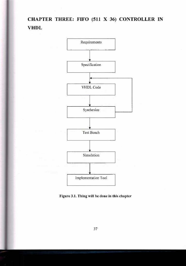
CHAPTER THREE: FIFO (511 X 36) C:ONTROLLER IN
VHDL
Requirements
,Ir
Specification
. ~ ,Ir
VHDL Code
,Ir
Synthesize
111'
Test Bench
,1,
Simulation
'
Implementation Tool
Figure 3.1. Thing will be done in this chapter
37

3.1 Requirement •.
My requirement is a FIFO (511 X 35) controller.
3.2 Specifications
3.2.1 FIFOs Using Virtex-11 Block RAM
I will describe a 511 X 36 FIFO; each port structure can be changed if the control
logic is changed accordingly. The size of the FIFO is 511 X 36 instead of
512 X 36 since one address is dropped out of the FIFO in order to provide distinct
Empty/Full conditions. First the design for a 511 X 36 with common Read and Write
clocks is described, and then the design changes required for the more difficult case of
independent Read and Write clocks are presented. Signal names in parenthesis are a
reference to the name in the VHDL code.
3.2.1.1 Synchronous FIFO Using Common Clocks
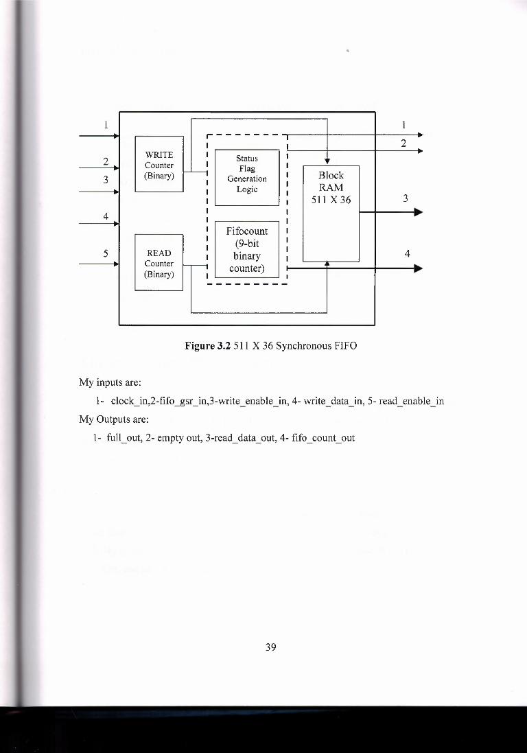
Figure 1 is a block diagram of a synchronous FIFO. When both the Read and
Write Clocks originate from the same source, it simplifies the operation and arbitration of
the FIFO, and the Empty and Full flags can be generated more easily. Binary counters are
used for both the read (read_addr) and write (write_addr) addresses counters. Table 1 lists
the Port Definitions for a synchronous FIFO design.
38
.•
1 :-
1 r----------.
2 - .
I .. I WRITE I Status I ,,
I 2 . Counter I Flag Block ~ I (Binary)
I Generation I RAM
3 Logic I
511 X 36 3 I .
I •.. I -., I I 4 - I I
I Fifocount I I (9-bit I I I 4 READ binary I •.. 5 I
••• - Counter -,, counter) --..
I (Binary) I ---------
Figure 3.2 511 X 36 Synchronous FIFO
My inputs are:
1- clock_in,2-fifo_gsr_in,3-write_enable_in, 4- write_data_in, 5- read_enable_in
My Outputs are:
1- full_out, 2- empty out, 3-read_data_out, 4- fifo_count_out
39

Table 3.1 Port Definitions
Signal Name Port Direction Port Width
Clock in input 1
Fifo _gsr _in input 1
Write enable in input 1 - - Write data in input 36 - -
Read enable in input 1 - - Read data out output 36 - - Full out output 1
Empty_out output 1
Fifocount out output 4
3.2.1.2 Synchronous FIFO operation
To perform a read, Read Enable (read_enable) is driven high prior to a rising
clock edge, and the Read Data (read_data) will be presented on the outputs during the
next clock cycle To do a Burst Read, simply leave Read Enable High for as many clock
cycles are desired, but if empty goes active after reading, then the last word has been
read, and the next Read Data would be invalid.
To perform a write, the Write Data (write_data) must be present on the inputs, and
Write Enable (write_enable) is driven high prior to a rising clock edge. As long as the
Full flag is not set, the write will be executed. To do a Burst Write, the Write Enable is
left High, and new Write Data must be available every cycle.
40

A FIFO count (fifocount) is added for convenience, to-determine when the FIFO
is Y:z full, % full, etc .. , as shown in Table 3. Its binary count of the number of words
currently stored in the FIFO. It is incremented on Writes, decremented on Reads, and left
alone when the operations performed within the same clock cycle. In this application only
the upper four bits are sent to VO, but that can easily be modified.
The Empty flag is set when either the fifocount is zero, or when the fifocount is
one and only a Read is being performed. This early decoding allows Empty to be set
immediately after the last Read. It is cleared after the Write operation (with no
simultaneous Read). Similarly, the Full flag is set when the fifocount is 511, or when the
fifocount is 510 and only a Write is being performed. It is cleared after a Read operation
(with no simultaneous Write). If the both Read and Write are done in the same clock
cycle, there is no change to the status flag. During Global Reset (fifo_gsr), both these
signals are driven high , to prevent any external logic from interfacing with the FIFO
during this time.
41

3.2.1.3 Asynchronous FIFO Using Independent Clocks
Figure 3.3 is the block diagram for a 511 X 36 asynchronous FIFO. The
asynchronous FIFO Read and Write port signals are clocked by independent Read and
Write clocks. Table 2 shows the port definition for an asynchronous FIFO.
1 . WRITE 1 . --------------- .
2 Counter --,.
I 2 . (Binary) Binary to FIFO Status .
3 Gray Code Flag I .
. I . Converter Generation Block
4 (WRITE) I RAM
. Logic I 3 . I 511 X 36 .
5 •.
. READ Binary to 9-Bit FIFO I . 6 Counter Gray Code Status I
. (Binary) Converter Register I
(READ) I I 4 .
L-------------- I
Figure 3.3 511 X 36 Asynchronous FIFO
The inputs are:
1- write_clock_in, 2- write_enable_in, 3- write_data_in, 4- read_clock_in
5- read_enable_in, 6- fifo_gsr_in.
The outputs are:
1- fifostatus_out, 2- full_out, 3- empty_out, 4- read_data_out.
42

Table 3.2 Port Definitions
Signal Name Port Direction Port Width
Write clock in Input 1 - - Read clock in Input 1 - - Fifo_gsr_in input 1
Write enable in input 1 - -
Write data in input 36 - -
Read enable in output 1 - -
Read data out output 36 - -
Full out output 1
Empty_out output 1
Fifostatus out output 4
3.2.1.4 Asynchronous FIFO operation
In order to operate a FIFO with independent Read and Write clocks, some
asynchronous arbitration logic is needed to determine the status flag. The previous
Empty/Full generation logic and associated flip-flops are no longer reliable, because they
are now asynchronous with respect to one another, since empty is clocked by the Read
clock, and full is clocked by the Write clock.
To solve this problem, and to minimize the speed of the control logic, additional
logic complexity is accepted for increased performance. There are primary 9-bit Read
and Write binary address counters, which drive the address inputs to the block RAM. The
binary addresses are converted to Gray-code, and pipelined for a few stages to create
several address pointers (read_addrgray, read_nextgray, read_lastgray, write_addrgray,
43

write_nextgray) which are used to generate the Full and Empty flags as quickly as
possible.
Gray-code addresses are used so that the registered Full and Empty flags
are always clean, and never in an unknown state due to the asynchronous relationship of
the Read and Write clocks. In the worst case scenario, Full and Empty would simply stay
active one cycle longer, but this would not generate an error.
When the Read and Write Gray-code pointers are equal, the FIFO is
empty. When the Read and Write Gray-code pointer is equal to the next Gray-code
pointer, the FIFO is full, having 511 (36-bit) words stored. Additional comparisons are
done within the same carry chain to determine when the FIFO is almost Empty and
almost Full, so that Empty and Full can be generated on the same clock edge as the last
operation. (Traditional control uses an asynchronous signal to test the flags, but this is
much slower and limits the overall performance.)
The fifostatus signal indicates Y:z full, Yi full, etc., as shown in Table 3. the
task of generating fifostatus in the asynchronous version is more complex, and therefore
requires more logic. The overall performance can be improved if this signal is trimmed.
The fifostatus outputs have a one-cycle latency for write operations, and a two-cycle
latency for reads.
44

..
Table 3.3 FIFO count and FIFO status signal Description
Bit 3 Bit 2 Bit 1 Bit 0 FIFOStatus/FIFOCount
1 1 1 1 15/16 full
1 1 1 0 7 /8 full
1 1 0 1 13/16 full
1 1 0 0 3/4 full
1 0 1 1 11/16 full
1 0 1 0 5/8 full
1 0 0 1 9/16 full
1 0 0 0 1/2 full
0 1 1 1 7 /16 full
0 1 1 0 3/8 full
0 1 0 1 5/16 full
0 1 0 0 1/4 full
0 0 1 1 3/16 full
0 0 1 0 1/8 full
0 0 0 1 1/16 full
0 0 0 0 < 1/16 full
3.2.1.5 Conclusion
The Virtex II block RAM can be used to generate both synchronous and
asynchronous FIFOs. Asynchronous FIFOs are possible due to the true dual-port nature
of the block RAM feature. These FIFOs can be operate at speeds around 200 MHz.
45

3.3 How I have Created My Project ..
To create project I did the following:
1. I have selected File/New Project ... That Will Make the New Project Wizard
to Appear.
Open Project . OpenEx~ . Close Project Save Project As ...
DNew ClrltN .; Open ... Clr1+0
dose -- iJ 5'Ve Ctrl+5
S.veAs ... fl 5'VeA! ---tl~lb~i
Frint Preview ... ~ Pr'1t... Ctrl+P ------··-··---·, I
Recent Fies
Recent Projects
lilt Piocesses I http:/t.w.w.><ilinx.com
Started "Launching De3ign Swrmary".
Figure 3.4 Creating new Project
2. Typing fifo_ctlr in the Project Name field will name the project fifo_ctlr.
46

Enter a Name and Location for the Proiect
Project Name: Project Location lm~_ctlr j j-C-:\X-ilinx---91-i\-sil ..•.. ent-\f-~o-_c_tl .•... r ......•... ----- ••.• , Q
Select the Type of T op·Level Source fo1 the Project Top-Level SotifoeJ ype:
{HDL
< Back t( Next > J More Info Cancel
Figure 3.5 Naming new Project
3. Enter or browse to a location (directory path) for the new project. A tutorial
subdirectory is created automatically.
4. We should verify that HDL is selected from the Top-Level Source Type list.
5. Clicking Next allows us to move to the device properties page.
6. I've filled the properties in the table as shown below:
• Product Category: All
47
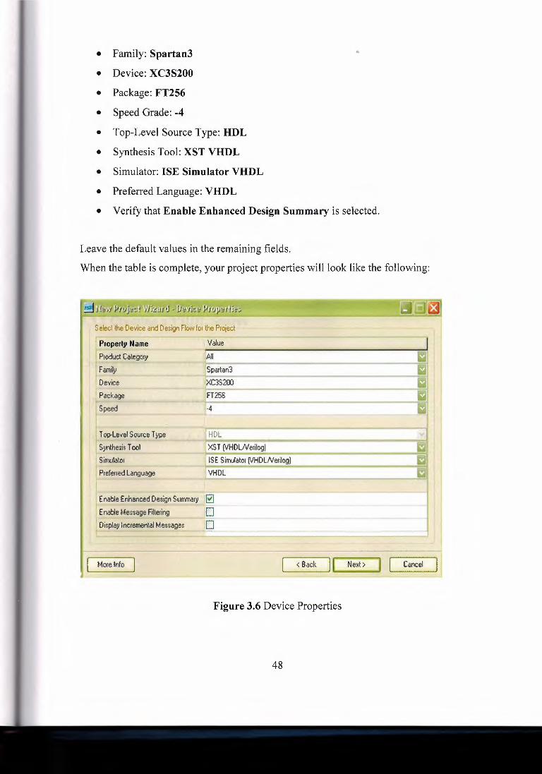
• Family: Spartan3 ••
• Device: XC3S200
• Package: FT256
• Speed Grade: -4
• Top-Level Source Type: HDL
• Synthesis Tool: XST VHDL
• Simulator: ISE Simulator VHDL
• Preferred Language: VHDL
• Verify that Enable Enhanced Design Summary is selected .
Leave the default values in the remaining fields.
When the table is complete, your project properties will look like the following:
Syn!!_)esis T e?I Simulator Prefeued Language
Select the Device and De~gn Flow- for the Project
f~perl;Na;e- ---1~ -- - ,.,._ _ ....;......;.._....;......;......;.._-1 oduct Category I AH I
1 Family ·-,,~~ 1 Spartan3 11
!Device- --·----~-"'~- 1XC3S200 - '.i.io"&_;,,;o-~~~~ ~
Package 'FT256 - ,,-~=~-- ~------------------....; Speed ·4 -..,..,...,.....,..,.,....;:..,..,....,.- ..•. ~- i _ _ 1__ __ ...._...._...._ ...._...._....___...._ __ --4
r Top-Level Sourc~ Type - """""" lj HDL : cl ' XST (v'HDLNerilog) Ii ISE Simulator (VHDLNerilog) VHDL
Enable Enhanced Design Summar1 Enable Message Filtering Display Incremental Messages
Moreh1fo Cancel
Figure 3.6 Device Properties
48

7. We click Next to proceed to the Create New Source window in the New Project
Wizard. At the end of the next section, new project will be complete.
3.3.1 Creating an HDL Source
In this section, I will show you how I have created a top-level HDL file for my
design.
A source file is any file that contains information about a design. Project
Navigator provides a wizard to help us create new source files for our project. If we are
targeting a Spartan-3A or Virtex-5 device, we can use the new source wizard to pre
assign package pins for an empty project. For details, Pre-Assigning Package Pins in the
New Source Wizard.
3.3.2 Creating a VHDL Source
Create a VHDL source file for the project as follows:
1. New Source button in the New Project Wizard.
2. Selecting VHDL Module as the source type.
49

3. Type in the file name FIFO 512 X 36 as follows. ..
\)' IP [Coregen & Architectuie Wizard) ol Schematic
~ User Document ~ Verilog Module
Verilog Test Fixture "NJ vBp~Module
VHDL Library PlVHDL Package yJ VHDL Test Bench
Fie name:
ltifo 51?X3~ Location:
lc:\Xilinx91i\silent\fifo_ctlr I 0
s I More_ Info c Back Next> Cancel
Figure 3.8 Source Type
4. We should verify that the Add to project checkbox is selected.
5. Click Next.
50

below in figure:
Entity Name lfifoctlr_cc_ v2
Arch~ecture Name !Behavioral I Port Name f Direction clock_in in
read_enable_in 1n
write_enable_in in write_data_in in
-------~'"' fifo_gsr_in lin read_data_out lout full_out I out --- empty_out out fifo_ count_ G1ut out
1n
I MSB I LSB
More Info < Back [ Cancel j
Figure 3.9 Declaring Ports
7. We click Next and then Finish in order in the New Source Wizard - Summary dialog
box to complete the new source file template.
8. We click Next, then Next, then Finish.
After finishing my Entity part which used to define the inputs and the outputs
,the result will be shown like this:
51

entity fifo _ ctlr is
port (clock_in:
•. IN std_logic;
read_enable_in: IN std_logic;
write_enable_in: IN std_logic;
write_data_in: IN std_logic_vector(35 downto O);
fifo_gsr_in: IN std_logic;
read_data_out: OUT std_logic_vector(35 downto O);
full_out: OUT std_logic;
empty_ out: OUT std _logic;
fifocount out: OUT std_logic_vector(3 downto O));
END fifo _ ctrl;
And then I wrote down the Architecture part which used to define the functions of
the design, the result would be shown like:
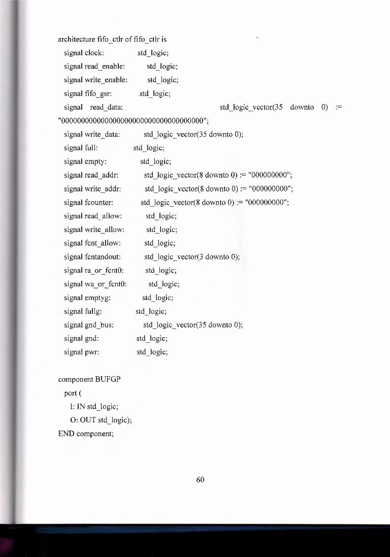
architecture fifo ctlr hdl of fifo ctlr is
signal clock:
signal read_ enable:
signal write_enable:
signal fifo _gsr:
signal read_ data:
std_logic;
std_logic;
std_logic;
std_logic;
std_logic_vector(35 downto 0)
:= "000000000000000000000000000000000000";
signal write_data: std_logic_ vector(35 downto O);
signal full: std_logic;
signal empty: std_logic;
signal read_addr: std_logic_vector(8 downto 0) := "000000000";
signal write_ addr: std _logic_ vector(8 down to 0) := "000000000";
signal fcounter: std _logic_ vector(8 downto 0) := "000000000";
signal read_allow: std_logic;
signal write_ allow: std _logic;
signal fcnt_allow: std_logic;
52

signal fcntandout:
signal ra_or_fcntO:
signal wa_or_fcntO:
signal emptyg:
signal fullg:
signal gnd_bus:
signal gnd:
signal pwr:
std _logic_ vector(3 downto O);
std_logic;
std_logic;
std_logic;
std_logic;
std _logic_ vector(3 5 down to O);
std_logic;
std_logic;
The next part I used to call the global buffer component which exists in the system:
component BUFGP
port (
I: IN std_logic;
0: OUT std_logic);
END component;
And here I have declared the block RAM codes which I described in my specification
section:
componentRAMB16_S36_S36
port (
ADDRA: IN std_logic_vector(8 downto O);
ADDRB: IN std_logic_vector(8 downto O);
DIA: IN std _logic_ vector(31 downto O);
DIB: IN std_logic_vector(31 downto O);
DIPA: IN std_logic_ vector(3 downto O);
DIPB: IN std_logic_ vector(3 downto O);
WEA: IN std_logic;
WEB: IN std_logic;
CLKA: IN std _logic;
CLKB: IN std_logic;
53

SSRA: IN std_logic;
SSRB: IN std_logic;
ENA: IN std_logic;
ENB: IN std_logic;
DOA: OUT std_logic_vector(31 downto O);
DOB: OUT std_logic_vector(31 downto O);
DOPA: OUT std_logic_vector(3 downto O);
DOPB: OUT std_logic_vector(3 downto O));
END component;
••
Now I am making a connection between the Entity part with my signal:
BEGIN
read_enable <= read_enable_in;
write_enable <= write_enable_in;
fifo_gsr <= fifo_gsr_in;
write_data <= write_data_in;
read_ data_ out <= read_ data;
full_ out <= full;
empty_ out <= empty;
gnd _ bus <= "000000000000000000000000000000000000";
gnd <= 'O';
pwr <= '1';
I had to instantiant a global buffer to make sure that there is no any skew problem
appears:
gclkl: BUFGP port map (I=> clock_in, 0 => clock);
54

Before the processes began, I had to connect my block RANI to the signal, and I have
done it using the following codes:
braml: RAMB16_S36_S36 port map (ADDRA => read_addr, ADDRB => write_addr,
DIA=> gnd_bus(35 downto 4), DIPA => gnd_bus(3 downto 0),
DIB => write_data(35 downto 4), DIPB => write_data(3 downto 0),
WEA => gnd, WEB => pwr, CLKA => clock, CLKB => clock,
SSRA => gnd, SSRB => gnd, ENA=> read_allow, ENB => write_allow,
DOA=> read_data(35 downto 4), DOPA=> read_data(3 downto 0) );
In my process case we have 7 different processes .I will try to obtain the processes as
following:
A. In the first two processes we have to set allow flags, which control the clock
enables for read, write, and count operations.
procl: PROCESS (clock, fifo_gsr)
BEGIN
IF ( fifo _gsr = '1 ') THEN
read_allow <= 'O';
ELS IF ( clock'EVENT AND clock = '1 ') THEN
read allow<= read enable AND NOT (fcntandout(O) AND fcntandout(l) - -
AND NOT write_allow);
END IF;
END PROCESS procl;
proc2: PROCESS (clock, fifo_gsr)
BEGIN
IF ( fifo _gsr = '1 ') THEN
write allow<= 'O'· - , ELSIF (clock'EVENT AND clock= '1 ') THEN
55

write allow<= write enable AND NOT (fcntandouuz) AND fcntandout(3) - - AND NOT read_allow);
END IF;
END PROCESS proc2;
fcnt_allow <= write_allow XOR read_allow;
B. When the empty flag is set on fifo_gsr (initial), or when on the next clock cycle,
Write Enable is low, and either the FIFOcount is equal to 0, or it is equal to 1
and Read Enable is high (about to go Empty).
ra_or_fcntO <= (read_allow OR NOT fcounter(O));
fcntandout(O) <= NOT (fcounter(4) OR fcounter(3) OR fcounter(2) OR fcounter(l)
OR fcounter(O));
fcntandout(l) <= NOT (fcounter(8) OR fcounter(7) OR fcounter(6) OR
fcounter(5));
emptyg <= (fcntandout(O) AND fcntandout(l) AND ra or fcntO AND NOT
write_allow);
proc3: PROCESS (clock, fifo_gsr)
BEGIN
IF (fifo_gsr = '1') THEN
empty<= '1';
ELS IF ( clock'EVENT AND clock = 'l ') THEN
empty <= emptyg;
END IF;
END PROCESS proc3;
C. Full flag is set on fifo _gsr (but it is cleared on the first valid clock edge after
fifo _gsr is removed), or when on the next clock cycle, Read Enable is low, and
56

either the FIFOcount is equal to lFF (hex), or it is equal to lFE and the Write
Enable is high (about to go Full).
wa_or_fcntO <= (write_allow OR fcounter(O));
fcntandout(2) <= (fcounter(4) AND fcounter(3) AND fcounter(2) AND
fcounter(l));
fcntandout(3) <= (fcounter(8) AND fcounter(7) AND fcounter(6) AND
fcounter(5));
fullg <= (fcntandout(2) AND fcntandout(3) AND wa or fcntO AND NOT
read_allow);
proc4: PROCESS (clock, fifo_gsr)
BEGIN
IF (fifo _gsr = '1 ') THEN
full<= '1';
ELS IF ( clock'EVENT AND clock = '1 ') THEN
full <= fullg;
END IF;
END PROCESS proc4;
D. The Generation of Read and Write address pointers are using binary counters,
because it is simpler in simulation, and the previous LFSR implementation
wasn't in the critical path. This is done for the process no. 5 & 6.
proc5: PROCESS (clock, fifo_gsr)
BEGIN
IF ( fifo _gsr = '1 ') THEN
read addr <= "000000000"· - ' ELS IF ( clock'EVENT AND clock = '1 ') THEN
IF (read_allow= '1') THEN
read_ addr <= read_ addr + '1 ';
57

END IF;
END IF;
END PROCESS proc5;
••
proc6: PROCESS (clock, fifo_gsr)
BEGIN
IF (fifo_gsr = '1') THEN write addr <= "000000000"·
- ' ELS IF ( clock'EVENT AND clock = 'l ') THEN IF (write_allow = 'l') THEN write_addr <= write_addr + '1';
END IF;
END IF;
END PROCESS proc6;
E. Generation of FIFOcount outputs. Used to determine how full FIFO is, based
on a counter that keeps track of how many words are in the FIFO. Also used to
generate Full and Empty flags. Only the upper four bits of the counter are sent
outside the module.
proc7: PROCESS (clock, fifo_gsr)
BEGIN
IF ( fifo _gsr = '1 ') THEN fcounter <= "000000000";
ELS IF ( clock'EVENT AND clock = 'l ') THEN IF (fcnt_allow = '1 ') THEN IF (read_allow = 'O') THEN fcounter <= fcounter + '1';
ELSE
fcounter <= fcounter - 'l';
END IF;
58

END IF;
END IF;
END PROCESS proc7;
..
fifocount out<= fcounter(8 downto 5);
END fifoctlr _cc_ v2 _hdl;
3.3.3 Open Codes of My FIFO (511 X 36) Design
library ieee;
use ieee.std_logic_l 164.all;
use ieee.std _logic_ unsigned.all;
-- synopsys translate_ off
library UNISIM;
use UNISIM.VCOMPONENTS.ALL;
-- synopsys translate_ on
entity fifo _ ctlr is
port (clock_in: IN std _logic;
read_enable_in: IN std_logic;
write_enable_in: IN std_logic;
write_data_in: IN std_logic_vector(35 downto O);
fifo_gsr_in: IN std_logic;
read_data_out: OUT std_logic_vector(35 downto O);
full_out: OUT std_logic;
empty_out: OUT std_logic;
fifocount out: OUT std_logic_vector(3 downto O));
END fifoctlr_cc_v2;
architecture fifo ctlr of fifo ctlr is - -
signal clock: std _logic;
signal read_enable:
signal write_enable:
signal fifo _gsr:
•.
std_logic;
std_logic;
std_logic;
signal read_ data: std _logic_ vector(35 downto 0)
"000000000000000000000000000000000000";
signal write_ data:
signal full:
signal empty:
signal read_ addr:
signal write_ addr:
signal fcounter:
signal read_ allow:
signal write_ allow:
signal fcnt_allow:
signal fcntandout:
signal ra_or_fcntO:
signal wa_or_fcntO:
signal emptyg:
signal fullg:
signal gnd_bus:
signal gnd:
signal pwr:
component BUFGP
port (
I: IN std_logic;
0: OUT std_logic);
END component;
std _logic_ vector(3 5 down to O);
std_logic;
std_logic;
std _logic_ vector(8 down to 0) := "000000000";
std_logic_ vector(8 downto 0) := "000000000";
std _logic_ vector(8 downto 0) := "000000000";
std_logic;
std_logic;
std_logic;
std _logic_ vector(3 downto O);
std_logic;
std_logic;
std_logic;
std_logic;
std_logic_ vector(35 downto O);
std_logic;
std_logic;
60

componentRAtv1Bl6_S36_S36
port (
ADDRA: IN std_logic_vector(8 downto O);
ADDRB: IN std_logic_vector(8 downto O);
DIA: IN std_logic_ vector(31 downto O);
DIB: IN std_logic_vector(31 downto O);
DIPA: IN std_logic_vector(3 downto O);
DIPB: IN std_logic_ vector(3 downto O);
WEA: IN std_logic;
WEB: IN std_logic;
CLKA: IN std_logic;
CLKB: IN std_logic;
SSRA: IN std_logic;
SSRB: IN std_logic;
ENA: IN std_logic;
ENB: IN std_logic;
DOA: OUT std _logic_ vector(31 downto O);
DOB: OUT std_logic_vector(31 downto O);
DOPA: OUT std _logic_ vector(3 downto O);
DOPB: OUT std_logic_vector(3 downto O));
END component;
BEGIN
read_enable <= read_enable_in;
write_enable <= write_enable_in;
fifo_gsr <= fifo_gsr_in;
write_data <= write_data_in;
read_ data_ out <= read_ data;
full_out <= full;
empty_ out <= empty;
gnd _ bus <= "000000000000000000000000000000000000";
61
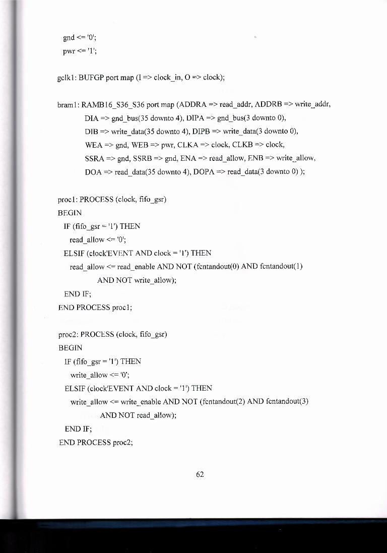
gnd <= 'O'· ' pwr <= '1';
..
gclkl: BUFGP port map (I => clock _in, 0 => clock);
braml: RAMB16_S36_S36 port map (ADDRA => read_addr, ADDRB => write_addr,
DIA=> gnd_bus(35 downto 4), DIPA => gnd_bus(3 downto 0),
DIB => write_data(35 downto 4), DIPB => write_data(3 downto 0),
WEA => gnd, WEB => pwr, CLKA => clock, CLKB => clock,
SSRA => gnd, SSRB => gnd, ENA=> read_allow, ENB => write_allow,
DOA=> read_data(35 downto 4), DOPA=> read_data(3 downto 0) );
procl: PROCESS (clock, fifo_gsr)
BEGIN
IF (fifo_gsr = 'l') THEN
read allow<= 'O'· - ' ELSIF (clock'EVENT AND clock= '1 ') THEN
read allow<= read enable AND NOT (fcntandout(O) AND fcntandout(l) - - AND NOT write_allow);
END IF;
END PROCESS procl;
proc2: PROCESS (clock, fifo_gsr)
BEGIN
IF ( fifo _gsr = '1 ') THEN
write allow<= 'O'· - ' ELS IF ( clock'EVENT AND clock = '1 ') THEN
write_allow <= write_enable AND NOT (fcntandout(2) AND fcntandout(3)
AND NOT read_allow);
END IF;
END PROCESS proc2;
62

••
fcnt_allow <= write_allow XOR read_allow;
ra_or_fcntO <= (read_allow OR NOT fcounter(O));
fcntandout(O) <= NOT (fcounter(4) OR fcounter(3) OR fcounter(2) OR fcounter(l) OR
fcounter(O));
fcntandout(l) <= NOT (fcounter(8) OR fcounter(7) OR fcounter(6) OR fcounter(5));
emptyg <= (fcntandout(O) AND fcntandout(l) AND ra or fcntO AND NOT
write_ allow);
proc3: PROCESS (clock, fifo_gsr)
BEGIN
IF ( fifo _gsr = 'l ') THEN
empty<= '1';
ELS IF ( clock'EVENT AND clock = '1 ') THEN
empty <= emptyg;
END IF;
END PROCESS proc3;
wa_or_fcntO <= (write_allow OR fcounter(O));
fcntandout(2) <= (fcounter(4) AND fcounter(3) AND fcounter(2) AND fcounter(l));
fcntandout(3) <= (fcounter(8) AND fcounter(7) AND fcounter(6) AND fcounter(5));
fullg <= (fcntandout(2) AND fcntandout(3) AND wa_or_fcntO AND NOT read_allow);
proc4: PROCESS (clock, fifo_gsr)
BEGIN
IF (fifo_gsr = '1') THEN
full<= '1 ';
ELS IF ( clock'EVENT AND clock = 'l ') THEN
full <= fullg;
END IF;
63

END PROCESS proc4; ..
proc5: PROCESS (clock, fifo_gsr)
BEGIN
IF ( fifo _gsr == '1 ') THEN
read_addr <== "000000000";
ELS IF ( clock'EVENT AND clock == 'l ') THEN
IF (read_allow == '1') THEN
read_ addr <== read_ addr + '1 '; END IF;
END IF;
END PROCESS proc5;
proc6: PROCESS (clock, fifo_gsr)
BEGIN IF ( fifo _gsr == '1 ') THEN
write_addr <== "000000000";
ELS IF ( clock'EVENT AND clock == '1 ') THEN
IF (write_allow == '1') THEN
write_addr <== write_addr + '1'; END IF;
END IF;
END PROCESS proc6;
proc7: PROCESS (clock, fifo_gsr)
BEGIN
IF ( fifo _gsr == '1 ') THEN
fcounter <== "000000000";
ELS IF ( clock'EVENT AND clock== '1 ') THEN
IF (fcnt_allow == 'l') THEN
IF (read_allow == 'O') THEN
64

fcounter <= fcounter + '1'; ELSE
fcounter <= fcounter - '1 ';
END IF;
END IF;
END IF;
END PROCESS proc7;
fifocount_out <= fcounter(8 downto 5);
END fifo_ctrl;
3.4 Synthesize
When the source files are complete, I had to check the syntax of the design to find errors
and types.
1. Firstly, verifying that Synthesis/Implementation is selected from the drop-down list
in the Sources window is the most important thing.
2. Selecting the fifo _ ctlr design source in the Sources window to display the related
processes in the Processes window.
3. The "+" used to expand the process group. (It's next to the Synthesize-XST process.)
4. Double-click the Check Syntax process.
Note: I used to correct any errors found in my source files. We can check for errors in
the Console tab of the Transcript window. Cause if you continue without valid syntax,
you will not be able to simulate or synthesize your design.
65

5. Then I closed the HDL file. •.
3.5 Test Bench of The Design
Now we need to test out design and we do it using the Test Bench tool for that.
We make sure that Synthesis/Implementation checked in source window, we mark on our
HDL design then click Project -+ New Source.
We should note that VHDL Test Bench must be checked on and we write fifo ctrl tb in
File name field. Then we click finish until we finish the process.
The figure below shows us:
'<J IP (Coiegen & Architecture Wizard) - MEM Fie
",J Implementation Constraints File State Diagram
.n. Test Bench Waveform
I E User Document Y Verilog Module
I Verilog Test Fixture I "w VHDL Module VHDL Libia,y I P VHDL Package
v VHDL Test Bench
[
Filename:
[fifo_ctrl_tb
Location:
jc:\Xainx91 i\silent\v2_filo_ vhd_258 ! 0
0 Add to project ______ ,,_ __ ~"~--~--' MOie lrfo <Back..J[_Next> ] I Cancel
Figure 3.10 Source Type
66

.. After clicking Finish, here is the result on Behavioral Simulation in source window:
LIBRARY ieee;
USE ieee.std_logic_l 164.ALL;
USE ieee.std _logic_ unsigned.all;
USE ieee.numeric _ std.ALL;
ENTITY fifo ctrl tb vhd IS - - -
END fifo_ctrl_tb_vhd;
ARCHITECTURE behavior OF fifo ctrl tb vhd IS
-- Component Declaration for the Unit Under Test (UUT)
COMPONENT fifo ctlr
PORT(
clock_in: IN std_logic;
read_enable_in: IN std_logic;
write_enable_in: IN std_logic;
write_data_in: IN std_logic_vector(35 downto O);
fifo_gsr_in: IN std_logic;
read_data_out: OUT std_logic_vector(35 downto O);
full_out: OUT std_logic;
empty_out: OUT std_logic;
fifocount_ out : OUT std _logic_ vector(3 downto 0)
);
END COMPONENT;
67

--Inputs
SIGNAL clock in: std Iogic := 'O';
SIGNAL read_enable_in: std Iogic := 'O';
SIGNAL write_enable_in: std_logic := 'O';
SIGNAL fifo_gsr_in: std_logic := 'O';
SIGNAL write_data_in: std_logic_vector(35 downto 0) := (others=>'O');
--Outputs
SIGNAL read_data_out: std_logic_vector(35 downto O);
SIGNAL full_out: std Iogic;
SIGNAL empty_out: stdIogic;
SIGNAL fifocount out: std_logic_vector(3 downto O);
BEGIN
-- Instantiate the Unit Under Test (UUT)
uut: fifoctlr _cc_ v2 PORT MAP(
clock _in=> clock _in,
read enable in=> read enable jn,
writeenable jn => write_enable_in,
write_data_in => write jlata jn,
fifo_gsr_in => fifo_gsr_in,
read , data_ out => read , data , out,
full , out=> full , out,
empty_ out => empty_ out,
fifocount out => fifocount out
);
68

••
tb: PROCESS
BEGIN
-- Wait 100 ns for global reset to finish
wait for 100 ns;
-- Place stimulus here
wait; -- will wait forever
END PROCESS;
END;
Here is my entity part which I used to define my Inputs/Outputs in it:
clock_in: IN std_logic;
read_enable_in: IN std_logic;
write_enable_in: IN std_logic;
write_data_in: IN std_logic_vector(35 downto O);
fifo_gsr_in: IN std_logic;
read_data_out: OUT std_logic_ vector(35 downto O);
full_out: OUT std_logic;
empty_out: OUT std_logic;
fifocount_ out : OUT std _logic_ vector(3 downto 0)
Afterwards I define my signals ( functions) in Architecture part:
--Inputs
SIGNAL clock in: std_logic := 'O';
SIGNAL read_enable_in: std_logic := 'O';
69

SIGNAL write_enable_in: std_logic := 'O'; .. SIGNAL fifo_gsr_in: std_logic := 'O';
SIGNAL write_data_in: std_logic_vector(35 downto 0) := (others=>'O');
--Outputs
SIGNAL read_data_out: std_logic_vector(35 downto O);
SIGNAL full_out: std_logic;
SIGNAL empty_out: std_logic;
SIGNAL fifocount out : std _logic_ vector(3 downto O);
Then I connect my Inputs/Outputs to my signal using these codes:
clock _in=> clock _in, read_enable_in => read_enable_in, write_enable_in => write_enable_in, write_data_in => write_data_in, fifo_gsr_in => fifo_gsr_in, read_ data_ out => read_ data_ out, full_out => full_out, empty_ out => empty_ out, fifocount out => fifocount out - -
I created a clock process using these:
elk _proc: process
begin clock _in<='O'; wait for 5 ns; clock_in<='l '; wait for 5 ns; end process;
I reset my FIFO giving a value 1 to my global reset, enabling to write by giving 1 and un
enabling to read by Oby:
tb: PROCESS BEGIN
70

fifo _gsr _in<=' 1 '; -- Wait 100 ns for global reset to finish wait for 100 ns;
write enable in<= '1 '· - - ' read_enable_in <= 'O'; fifo _gsr _in<='O';
write_data_in <= (write_data_in'range=>'O');
wait for 20 ns;
Afterward I made a loop of 511 to make sure that I used all of the FIFO without
bad addressing or errors, enabling the read and un-enabling and incrementing the write
process by:
for i in O to 511 loop write_data_in <= write_data_in + "10"; wait for 20 ns; end loop;
-- Place stimulus here read_enable_in <= '1'; write_enable_in <= 'O'; wait; -- will wait forever
After we have finished our coding we must make sure that we used correct codes,
we do it by using Checking Syntax tool, correct any syntax errors.
71

••
3.6 Simulation
I can simply reach the Simulation tool by selecting Behavioral Simulation from
the Source Window, and then Xilinx ISE Simulator ~ Simulate Behavioral Model
from the Process window. As shown in the figure below:
'-~v2..lifo_l'hd_258 t::h:3s100e-4tq144 ~-~IJ~_cc)>_vhd,~(m.vhd)
tuU_ou~ •> !ul)_out, empey_out •> empty_out, tUocount out •> titocount out
52 ) ; - - 53
55 S6 begin
~:!s f(J: floctk_cc_tb_ vhd · ~ r- r:l Add E~sting Souce '-o Creale New Swi;e S·» XinidSE S~oc
'f ,~ Check SJ"la.
57 clock in<:=101;
Sa 'i,ait tor s ns; 5~ cloclt_in<•' 1'; 60 vait tor S ns; 61 enct process; 62 '63 64 tb : PROCESS 65 BEGIN 66 tifo gsr in<•' 1'; 67 _: llait 100 tis .to~ global reset to tinish 6S 11ait tor 100 ns: 69 vriu eneble in <• '1'; 70 read_enable_in <• '0'; ?1 7~ 73 74 75 76
vrite_data_in <• (wdt1t_data_in' range•>' 0');
vait for 20 ns; tor i in O to 511 loop
run all stop -s Stopped at line•S9 tile nameaC: / Ki linx911/ si lent/v2 _f if_o _ vhcl _2 58/ aaa. vhd
Fild,1 fries 1
Figure 3.11 Simulation the Design
72

..
Running Simulation causes us to get these results:
Figure 3.12 Simulation Result
As we can see from the figure. When the global reset goes from 1 to 0, the
resetting process stops. And when the write_enable_in become 1, it starts to write into the
FIFO.
We should note that the write_data_in is increasing 2 by 2 that's the cause of our shown
code:
write_data_in <= write_data_in + "10";
73

..
And here is another screen shot which shows us that after a certain time the
read_ data_ out is also increasing, as shown below:
Figure 3.13 Simulation Result
This means that I wrote data in my FIFO and I can read them, and that was my objective.
74
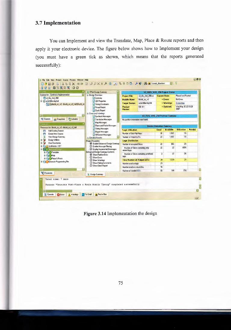
3. 7 Implementation ••
You can Implement and view the Translate, Map, Place & Route reports and then
apply it your electronic device. The figure below shows how to Implement your design
(you must have a green tick as shown, which means that the reports generated
successfully):
"}'.: Fae Edi: 1/iew Project Sou',e ,. f'°'"'' Wlidow HelJ 110 ~ ~ c,.t~~rn~~xtl\')e1 ftijfof':rcx;l!,,@i~~~ s III gig> 111 i100~1§:dfect?':' ih Q
0 t!'Ht~~~~(H)
NoErrois
~ i Wed Ma,, 30 23:19:28 !i 2007
C1eate New Souce View Design S\.1Yl1l'1¥y De~Utitie$ u~Ct>nS:traints Si,,tt>esize·XST
(~~Tron,late $ ,~$Map $--'~Place & Route ,~@GeneioteProg,amfringF'rle
r Total time: 7 :,;;'c~ I
Process -cenecaee pcet.-p Iece & Route Static:: Timing" completed eucceeerut tv
Figure 3.14 Implementation the design
75

Conclusion ..
I designed a FIFO Controller using Integrated Software Environment (ISE)
development tools. My design approach was to define my inputs, outputs and functions
using the VHDL, generated a Test Bench to write into 512 location with different data,
and to read this 512 data location one-by-one. I used the Test Bench Simulator Tool to
see what I wrote I read it back. The simulation was successful, that means I have read the
data correctly.
I used 5 different functions (processes) to fill the locations of my FIFO, and here
they are:
• I set allow flags, which control the clock enables for read, write, and count
operations.
• Empty flag is set on fifo _gsr (initial), or when on the next clock cycle,
Write Enable is low, and either the FIFOcount is equal to 0, or it is equal
to 1 and Read Enable is high (about to go Empty).
• Full flag is set on fifo _gsr (but it is cleared on the first valid clock edge
after fifo_gsr is removed), or when on the next clock cycle, Read Enable is
low, and either the FIFOcount is equal to lFF (hex), or it is equal to lFE
and the Write Enable is high (about to go Full).
• Generation of Read and Write address pointers. They now se binary
counters, because it is simpler in simulation, and the previous LFSR
implementation wasn't in the critical path.
• Generation of FIFO count outputs. Used to determine how full FIFO is,
based on a counter that keeps track of how many words are in the FIFO.
Also used to generate Full and Empty flags. Only the upper four bits of
the counter are sent outside the module.
76
-----------

Conclusion
I designed a FIFO (511X36) Controller using VHDL. I have used the Integrated
Software Environment (ISE) development tools to develop and implement the project.
My design approach was to define the requirements of the design, then derive the
specification. I wrote my VHDL codes defining my inputs, outputs and functions (I used
5 different processes to design the function of the FIFO) my functions were signals, so I
used to connect my entity part to my signal. I used the synthesis tool to check my design
syntax then I generated a Test Bench to write into 512 locations with different data, and
to read this 512 data location one-by-one (I made a FOR loop of 511 to make sure that I
used all of the FIFO without bad addressing or errors, enabling the read and un-enabling
and incrementing the write process). Checked the Syntax and everything was under
control.
I used the Test Bench Simulator Tool to see what I wrote I read it back then I
have created some implement reports like (translate, map, place & route). The simulation
was successful; the codes are ready to be uploaded into the electronic device, which
means I have reached my objective.
76

REFERENCES
• Xilinx ISE Software Manual.
• Xilinx ISE Application Notes.
• Xilinx ISE Tutorials: Xilinx ISE Quick Start and Xilinx ISE Tutorials on the
Web.
• Xilinx ISE Web Page.
77