nanoscale - connecting repositories yin,ab yashu zang,a binbin xu,c shuping li,a junyong kang,a...
TRANSCRIPT
Nanoscale
PAPER
Publ
ishe
d on
30
Sept
embe
r 20
13. D
ownl
oade
d by
Xia
men
Uni
vers
ity o
n 12
/07/
2015
15:
47:4
7.
View Article OnlineView Journal | View Issue
aDepartment of Physics/Pen-Tung Sah Institu
Xiamen University, Xiamen, 361005, China.
2187196; Tel: +86-592-2181340bWuhan National Laboratory for Optoelect
Information, Huazhong University of Scie
China. E-mail: [email protected]
87793024cCollege of Chemistry and Chemical Enginee
China
Cite this: Nanoscale, 2014, 6, 3934
Received 5th August 2013Accepted 29th September 2013
DOI: 10.1039/c3nr04106a
www.rsc.org/nanoscale
3934 | Nanoscale, 2014, 6, 3934–3940
Multipole plasmon resonances in self-assembledmetal hollow-nanospheres
Jun Yin,ab Yashu Zang,a Binbin Xu,c Shuping Li,a Junyong Kang,a Yanyan Fang,b
Zhihao Wu*b and Jing Li*a
Recently, multipole plasmonic mode resonances in metal hollow structures, such as dipole, quadrupole,
and octupole modes, have been widely investigated by researchers with the aim for potential
applications in bio-sensing, fluorescence, nanolasers or nonlinear nano-photonics. Here, in this work,
the multipole plasmon resonances in self-assembled metal hollow-nanospheres (HNSs) are theoretically
and experimentally demonstrated and the hot spots originating from the higher order mode plasmonic
resonance and interparticle coupling effect are proposed to be used for Raman scattering
enhancements. Dipole, quadrupole, octupole and hexadecapole mode plasmonic resonances were
clearly resolved in the extinction spectra of these Ag HNS arrays showing good agreement with the
theoretical simulation results. Strong regular hot spots were obtained around the surface and in the gaps
of the Ag HNSs through the higher order mode plasmonic resonances and corresponding interparticle
coupling effect between the HNSs. Maximum local field intensity was accomplished by optimizing the
size of as well as the coupling distance between the HNSs and then it was applied to SERS sensing.
Raman mapping also demonstrated these self-assembled plasmonic cavity arrays to be a stable and
uniform SERS-active substrate.
Introduction
Surface plasmon based surface-enhanced Raman scattering(SERS)1 is a leading non-destructive technique that helps toextend the sensitivity of Raman spectroscopy to the level of asingle molecule.2,3 Generally, the strongly enhanced local near-eld originating from the surface plasmon resonance (SPR)effect on the metal nanostructures is the main mechanism forsurface plasmon based SERS.4 In recent years, a large local near-eld enhancement generated from the local surface plasmonresonance (LSPR) effect in a specic region around or its inter-coupling effect between metal NPs, which is dened as a ‘hotspot’, has drawn researchers' attention and been widelyproposed and demonstrated for single molecule level detec-tion.5–7 Due to the special geometries with controllablemorphologies and parameters,8–10 adjustable plasmon bands9,10
and resonance modes11–15 can be easily realized in metal hollownano-structures. Thus, they have been extensively studied and
te of Micro-Nano Science and Technology,
E-mail: [email protected]; Fax: +86-592-
ronics, School of Optical and Electronic
nce and Technology, Wuhan, 430074,
n; Fax: +86-27-87793035; Tel: +86-27-
ring, Xiamen University, Xiamen, 361005,
applied to highly sensitive SERS sensing given the highlylocalized near-eld7,15 and the corresponding regular hot spotsaround the nanoparticles.16–19 M. A. Mahmoud and his co-workers have symmetrically investigated both the surface plas-mon resonance and the coupling properties of gold hollownanocages by optimizing the size and shell thickness aiming forhighly sensitive SERS detection.18
Multipole SPR modes on gold or silver nanostructures, such ascore shells,7,8,20 nanoprisms,21 nanorods22,23 or spherical parti-cles,24,25 have been observed in previous studies. Recently, thesemultipole plasmonic resonance modes in metal shells or cavitystructures have gained much renewed attention due to thepotential applications in bio-sensing,26 uorescence,27 nano-lasers,28,29 or nonlinear nano-photonics.30 Commonly, a highlylocalized electromagnetic eld can be obtained in or on the plas-monic cavities through the resonances in multipole modes, whichhave been proposed to create high quality (Q) factor plasmonicresonators31,32 or ultra-small-mode-volume devices, e.g. nano-lasers, surface plasmon amplication by stimulated emission ofradiation (SPASER), etc.28,29 Additionally, by using the highlylocalized electromagnetic elds on the exterior surface of a plas-monic resonator, in which plasmonic whispering-gallery mode(WGM) resonance happens, the cavity can be potentially used as aWGM resonator based bio-sensor with a high sensitivity of up to500 nm per refraction index unit, and wide detection range.26
Here, in this work, multipole plasmon resonances wererealized in the self-assembled Ag hollow-nanospheres (HNSs).
This journal is © The Royal Society of Chemistry 2014
Paper Nanoscale
Publ
ishe
d on
30
Sept
embe
r 20
13. D
ownl
oade
d by
Xia
men
Uni
vers
ity o
n 12
/07/
2015
15:
47:4
7.
View Article Online
Beneting from higher order plasmonic resonances, a highlylocalized near-eld around the surface and hot spots generatedby the inter-coupling effect in the gaps were obtained within theHNS arrays, which were then demonstrated to be an ideal SERSsubstrate by taking advantage of these enhanced local elds.The large scale two-dimensional (2D) Ag HNS arrays werefabricated using the self-assembled polystyrene (PS) nano-spheres as the template with its size and gaps adjusted byemploying reactive-ion etching (RIE) on the template. Dipole,quadrupole, octupole and hexadecapole mode plasmonic reso-nances are distinguishably resolved from the extinction spectrashowing good agreement with the simulated spectra and near-eld distributions. According to the FDTD simulation results,highly localized electromagnetic eld distribution and strongregular hot spots were obtained around or in the gaps betweenthe Ag HNSs through the interparticle coupling effect, which arebelieved to be responsible for the highly sensitive SERSperformance on the Ag HNS arrays with the optimized size andgaps. Further Raman mapping from this metal hollow structureevidences these periodic plasmonic cavity arrays to be a stableand uniform SERS-active substrate.
Experimental details
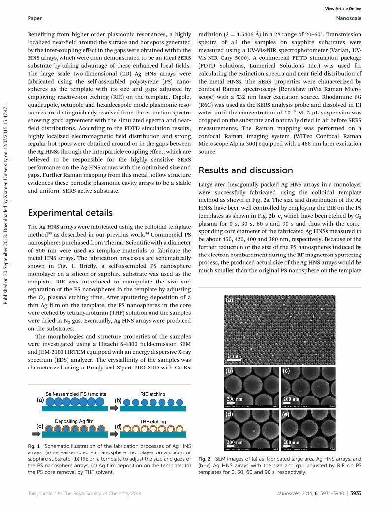
The Ag HNS arrays were fabricated using the colloidal templatemethod33 as described in our previous work.34 Commercial PSnanospheres purchased from Thermo Scientic with a diameterof 500 nm were used as template materials to fabricate themetal HNS arrays. The fabrication processes are schematicallyshown in Fig. 1. Briey, a self-assembled PS nanospheremonolayer on a silicon or sapphire substrate was used as thetemplate. RIE was introduced to manipulate the size andseparation of the PS nanospheres in the template by adjustingthe O2 plasma etching time. Aer sputtering deposition of athin Ag lm on the template, the PS nanospheres in the corewere etched by tetrahydrofuran (THF) solution and the sampleswere dried in N2 gas. Eventually, Ag HNS arrays were producedon the substrates.
The morphologies and structure properties of the sampleswere investigated using a Hitachi S-4800 eld-emission SEMand JEM-2100 HRTEM equipped with an energy dispersive X-rayspectrum (EDS) analyzer. The crystallinity of the samples wascharacterized using a Panalytical X'pert PRO XRD with Cu-Ka
Fig. 1 Schematic illustration of the fabrication processes of Ag HNSarrays: (a) self-assembled PS nanosphere monolayer on a silicon orsapphire substrate; (b) RIE on a template to adjust the size and gaps ofthe PS nanosphere arrays; (c) Ag film deposition on the template; (d)the PS core removal by THF solvent.
This journal is © The Royal Society of Chemistry 2014
radiation (l ¼ 1.5406 A) in a 2q range of 20–60�. Transmissionspectra of all the samples on sapphire substrates weremeasured using a UV-Vis-NIR spectrophotometer (Varian, UV-Vis-NIR Cary 5000). A commercial FDTD simulation package(FDTD Solutions, Lumerical Solutions Inc.) was used forcalculating the extinction spectra and near eld distribution ofthe metal HNSs. The SERS properties were characterized byconfocal Raman spectroscopy (Renishaw inVia Raman Micro-scope) with a 532 nm laser excitation source. Rhodamine 6G(R6G) was used as the SERS analysis probe and dissolved in DIwater until the concentration of 10�5 M. 2 mL suspension wasdropped on the substrate and naturally dried in air before SERSmeasurements. The Raman mapping was performed on aconfocal Raman imaging system (WITec Confocal RamanMicroscope Alpha 300) equipped with a 488 nm laser excitationsource.
Results and discussion
Large area hexagonally packed Ag HNS arrays in a monolayerwere successfully fabricated using the colloidal templatemethod as shown in Fig. 2a. The size and distribution of the AgHNSs have been well controlled by employing the RIE on the PStemplates as shown in Fig. 2b–e, which have been etched by O2
plasma for 0 s, 30 s, 60 s and 90 s and thus with the corre-sponding core diameter of the fabricated Ag HNSs measured tobe about 450, 420, 400 and 380 nm, respectively. Because of thefurther reduction of the size of the PS nanospheres induced bythe electron bombardment during the RF magnetron sputteringprocess, the produced actual size of the Ag HNS arrays would bemuch smaller than the original PS nanosphere on the template
Fig. 2 SEM images of (a) as-fabricated large area Ag HNS arrays, and(b–e) Ag HNS arrays with the size and gap adjusted by RIE on PStemplates for 0, 30, 60 and 90 s, respectively.
Nanoscale, 2014, 6, 3934–3940 | 3935
Nanoscale Paper
Publ
ishe
d on
30
Sept
embe
r 20
13. D
ownl
oade
d by
Xia
men
Uni
vers
ity o
n 12
/07/
2015
15:
47:4
7.
View Article Online
aer the RIE. Therefore, the diameter of the Ag HNSs on thesample with 0 s of RIE is �450 nm, which is smaller than theoriginal diameter of 500 nm for PS nanospheres in the template,so do other samples. Understandably, the gaps between the AgHNSs can also be adjusted by controlling the RIE time.
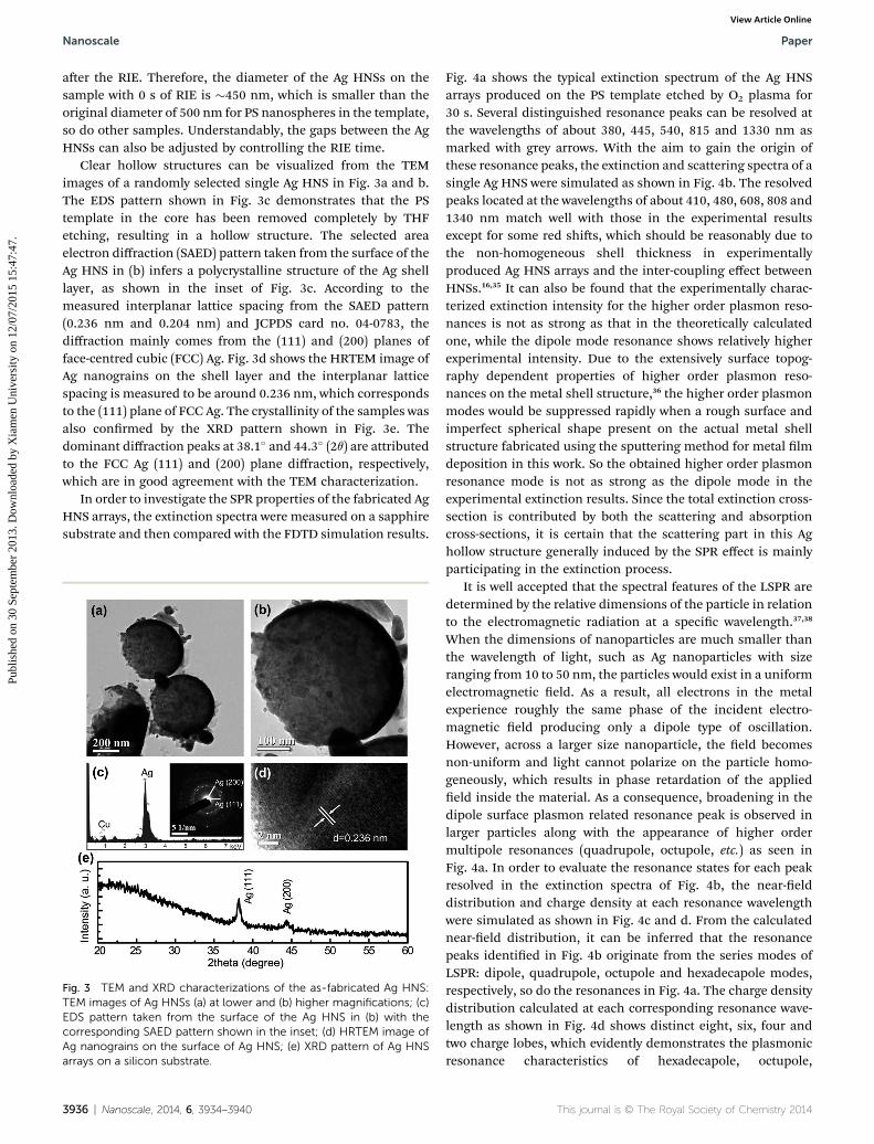
Clear hollow structures can be visualized from the TEMimages of a randomly selected single Ag HNS in Fig. 3a and b.The EDS pattern shown in Fig. 3c demonstrates that the PStemplate in the core has been removed completely by THFetching, resulting in a hollow structure. The selected areaelectron diffraction (SAED) pattern taken from the surface of theAg HNS in (b) infers a polycrystalline structure of the Ag shelllayer, as shown in the inset of Fig. 3c. According to themeasured interplanar lattice spacing from the SAED pattern(0.236 nm and 0.204 nm) and JCPDS card no. 04-0783, thediffraction mainly comes from the (111) and (200) planes offace-centred cubic (FCC) Ag. Fig. 3d shows the HRTEM image ofAg nanograins on the shell layer and the interplanar latticespacing is measured to be around 0.236 nm, which correspondsto the (111) plane of FCC Ag. The crystallinity of the samples wasalso conrmed by the XRD pattern shown in Fig. 3e. Thedominant diffraction peaks at 38.1� and 44.3� (2q) are attributedto the FCC Ag (111) and (200) plane diffraction, respectively,which are in good agreement with the TEM characterization.
In order to investigate the SPR properties of the fabricated AgHNS arrays, the extinction spectra were measured on a sapphiresubstrate and then compared with the FDTD simulation results.
Fig. 3 TEM and XRD characterizations of the as-fabricated Ag HNS:TEM images of Ag HNSs (a) at lower and (b) higher magnifications; (c)EDS pattern taken from the surface of the Ag HNS in (b) with thecorresponding SAED pattern shown in the inset; (d) HRTEM image ofAg nanograins on the surface of Ag HNS; (e) XRD pattern of Ag HNSarrays on a silicon substrate.
3936 | Nanoscale, 2014, 6, 3934–3940
Fig. 4a shows the typical extinction spectrum of the Ag HNSarrays produced on the PS template etched by O2 plasma for30 s. Several distinguished resonance peaks can be resolved atthe wavelengths of about 380, 445, 540, 815 and 1330 nm asmarked with grey arrows. With the aim to gain the origin ofthese resonance peaks, the extinction and scattering spectra of asingle Ag HNS were simulated as shown in Fig. 4b. The resolvedpeaks located at the wavelengths of about 410, 480, 608, 808 and1340 nm match well with those in the experimental resultsexcept for some red shis, which should be reasonably due tothe non-homogeneous shell thickness in experimentallyproduced Ag HNS arrays and the inter-coupling effect betweenHNSs.16,35 It can also be found that the experimentally charac-terized extinction intensity for the higher order plasmon reso-nances is not as strong as that in the theoretically calculatedone, while the dipole mode resonance shows relatively higherexperimental intensity. Due to the extensively surface topog-raphy dependent properties of higher order plasmon reso-nances on the metal shell structure,36 the higher order plasmonmodes would be suppressed rapidly when a rough surface andimperfect spherical shape present on the actual metal shellstructure fabricated using the sputtering method for metal lmdeposition in this work. So the obtained higher order plasmonresonance mode is not as strong as the dipole mode in theexperimental extinction results. Since the total extinction cross-section is contributed by both the scattering and absorptioncross-sections, it is certain that the scattering part in this Aghollow structure generally induced by the SPR effect is mainlyparticipating in the extinction process.
It is well accepted that the spectral features of the LSPR aredetermined by the relative dimensions of the particle in relationto the electromagnetic radiation at a specic wavelength.37,38
When the dimensions of nanoparticles are much smaller thanthe wavelength of light, such as Ag nanoparticles with sizeranging from 10 to 50 nm, the particles would exist in a uniformelectromagnetic eld. As a result, all electrons in the metalexperience roughly the same phase of the incident electro-magnetic eld producing only a dipole type of oscillation.However, across a larger size nanoparticle, the eld becomesnon-uniform and light cannot polarize on the particle homo-geneously, which results in phase retardation of the appliedeld inside the material. As a consequence, broadening in thedipole surface plasmon related resonance peak is observed inlarger particles along with the appearance of higher ordermultipole resonances (quadrupole, octupole, etc.) as seen inFig. 4a. In order to evaluate the resonance states for each peakresolved in the extinction spectra of Fig. 4b, the near-elddistribution and charge density at each resonance wavelengthwere simulated as shown in Fig. 4c and d. From the calculatednear-eld distribution, it can be inferred that the resonancepeaks identied in Fig. 4b originate from the series modes ofLSPR: dipole, quadrupole, octupole and hexadecapole modes,respectively, so do the resonances in Fig. 4a. The charge densitydistribution calculated at each corresponding resonance wave-length as shown in Fig. 4d shows distinct eight, six, four andtwo charge lobes, which evidently demonstrates the plasmonicresonance characteristics of hexadecapole, octupole,
This journal is © The Royal Society of Chemistry 2014
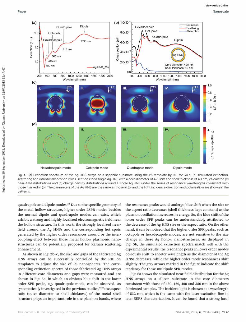
Fig. 4 (a) Extinction spectrum of the Ag HNS arrays on a sapphire substrate using the PS template by RIE for 30 s; (b) simulated extinction,scattering and intrinsic absorption cross-sections for a single Ag HNSwith a core diameter of 420 nm and shell thickness of 40 nm; calculated (c)near-field distributions and (d) charge density distributions around a single Ag HNS under the series of resonance wavelengths consistent withthosemarked in (b). The parameters of the Ag HNS are the same as those in (b) and the light incidence direction and polarization are shown in thepatterns.
Paper Nanoscale
Publ
ishe
d on
30
Sept
embe
r 20
13. D
ownl
oade
d by
Xia
men
Uni
vers
ity o
n 12
/07/
2015
15:
47:4
7.
View Article Online
quadrupole and dipole modes.39 Due to the specic geometry ofthe metal hollow structure, higher order LSPR modes besidesthe normal dipole and quadrupole modes can exist, whichexhibit a strong and highly localized electromagnetic eld nearthe hollow structure. In this work, the strongly localized near-eld around the Ag HNSs and the corresponding hot spotsgenerated by the higher order resonances around or the inter-coupling effect between those metal hollow plasmonic nano-structures can be potentially proposed for Raman scatteringenhancement.
As shown in Fig. 2b–e, the size and gaps of the fabricated AgHNS arrays can be successfully controlled by the RIE ontemplates to adjust the size of PS nanospheres. The corre-sponding extinction spectra of those fabricated Ag HNS arraysin different core diameters and gaps were measured and areshown in Fig. 5a, in which an obvious blue shi in the lowerorder SPR peaks, e.g. quadrupole mode, can be observed. Assystematically investigated in the previous studies,9,40 the aspectratio (outer diameter to shell thickness) of the metal shellstructure plays an important role in the plasmon bands, where
This journal is © The Royal Society of Chemistry 2014
the resonance peaks would undergo blue shi when the size orthe aspect ratio decreases (shell thickness kept constant) as theplasmon oscillation increases in energy. So, the blue shi of thelower order SPR peaks can be understandably attributed tothe decrease of the Ag HNS size or the aspect ratio. On the otherhand, it can be noticed that the higher order SPR peaks, such asoctupole or hexadecapole modes, are not sensitive to the sizechange in these Ag hollow nanostructures. As displayed inFig. 5b, the simulated extinction spectra match well with theexperimental results: the resonance peaks in lower order modesobviously shi to shorter wavelength as the diameter of the AgHNSs decreases, while the higher order mode resonances shislightly. The grey arrows marked in the gure indicate the shitendency for these multipole SPR modes.
Fig. 6a shows the simulated near-eld distribution for the AgHNS arrays on a silicon substrate in the core diametersconsistent with those of 450, 420, 400 and 380 nm in the abovefabricated samples. The incident light is chosen at a wavelengthof 532 nm, which is the same with the laser excitation line inlater SERS characterization. It can be found that a strong local
Nanoscale, 2014, 6, 3934–3940 | 3937
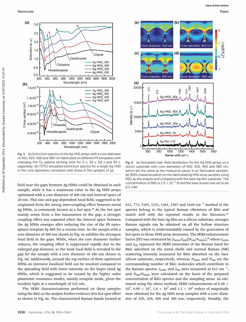
Fig. 5 (a) Extinction spectra of the Ag HNS arrays with a core diameterof 450, 420, 400 and 380 nm fabricated on different PS templates withchanging the O2 plasma etching time for 0 s, 30 s, 60 s and 90 s,separately; (b) FDTD simulated extinction spectra for a single Ag HNSin the core diameters consistent with those in the samples of (a).
Fig. 6 (a) Simulated near-field distribution for the Ag HNS arrays on asilicon substrate with core diameters of 450, 420, 400 and 380 nm,which are the same as the measured values in as-fabricated samples.(b) SERS characterization on the fabricated Ag HNS array samples usingR6G as the analyte and compared with the bare Ag film substrate. Theconcentration of R6G is 1.0� 10�5 M and the laser power was set to be0.5 mW.
Nanoscale Paper
Publ
ishe
d on
30
Sept
embe
r 20
13. D
ownl
oade
d by
Xia
men
Uni
vers
ity o
n 12
/07/
2015
15:
47:4
7.
View Article Online
eld near the gaps between Ag HNSs could be obtained in eachsample, while it has a maximum value in the Ag HNS arraysoptimized with a core diameter of 400 nm and interval space of20 nm. This size and gap dependent local eld, suggested to beoriginated from the strong inter-coupling effect between metalAg HNSs, is commonly known as a hot spot.16 As the hot spotmainly arises from a few nanometers in the gap, a strongercoupling effect was expected when the interval space betweenthe Ag HNSs emerges aer reducing the size of the PS nano-sphere template by RIE for a certain time. So the sample with acore diameter of 400 nm shown in Fig. 6c exhibits the strongestlocal eld in the gaps. While, when the core diameter furtherreduces, the coupling effect is suppressed rapidly due to theenlarged gap distance, so the weak local eld is revealed in thegap for the sample with a core diameter of 380 nm shown inFig. 6d. Additionally, around the top surface of these optimizedHNSs an intensive localized eld can be resolved compared tothe spreading eld with lower intensity on the larger sized AgHNSs, which is suggested to be caused by the higher orderplasmonic resonance modes, mainly octupole mode, given theincident light at a wavelength of 532 nm.
The SERS characterizations performed on these samplesusing the R6G as the analyte further evidence this hot spot effectas shown in Fig. 6e. The characterized Raman bands located at
3938 | Nanoscale, 2014, 6, 3934–3940
611, 773, 1185, 1311, 1361, 1507 and 1649 cm�1 marked in thespectra belong to the typical Raman vibrations of R6G andmatch well with the reported results in the literature.41
Compared with the bare Ag lm on a silicon substrate, strongerRaman signals can be obtained on all the hollow structuresamples, which is understandably caused by the generation ofhot spots in those HNS array structures. The SERS enhancementfactor (EF) was estimated by (ISERS/INR)(NNR/NSERS),42 where ISERSand INR represent the SERS intensities of the Raman band forR6G adsorbed on the metal shells and normal Raman (NR)scattering intensity measured for R6G absorbed on the baresilicon substrate, respectively, whereas NSERS and NNR are thecorresponding number of R6G molecules which contribute tothe Raman spectra. ISERS and INR were measured at 611 cm�1,and NNR/NSERS were calculated on the basis of the preparedconcentration of R6G species and the sampling areas. As esti-mated using the above method, SERS enhancements of 0.48 �105, 0.90 � 105, 1.6 � 105 and 1.1 � 105 orders of magnitudewere obtained for the Ag HNS array samples with a core diam-eter of 450, 420, 400 and 380 nm, respectively. Notably, the
This journal is © The Royal Society of Chemistry 2014
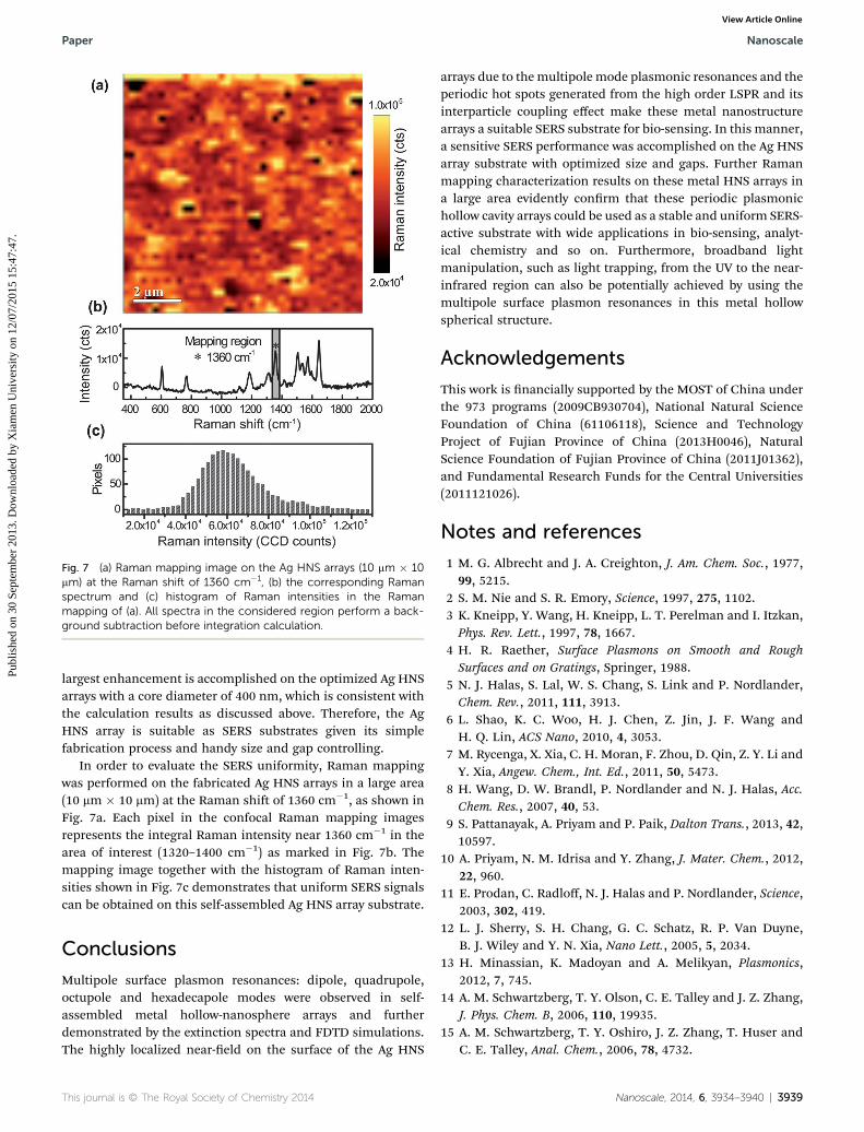
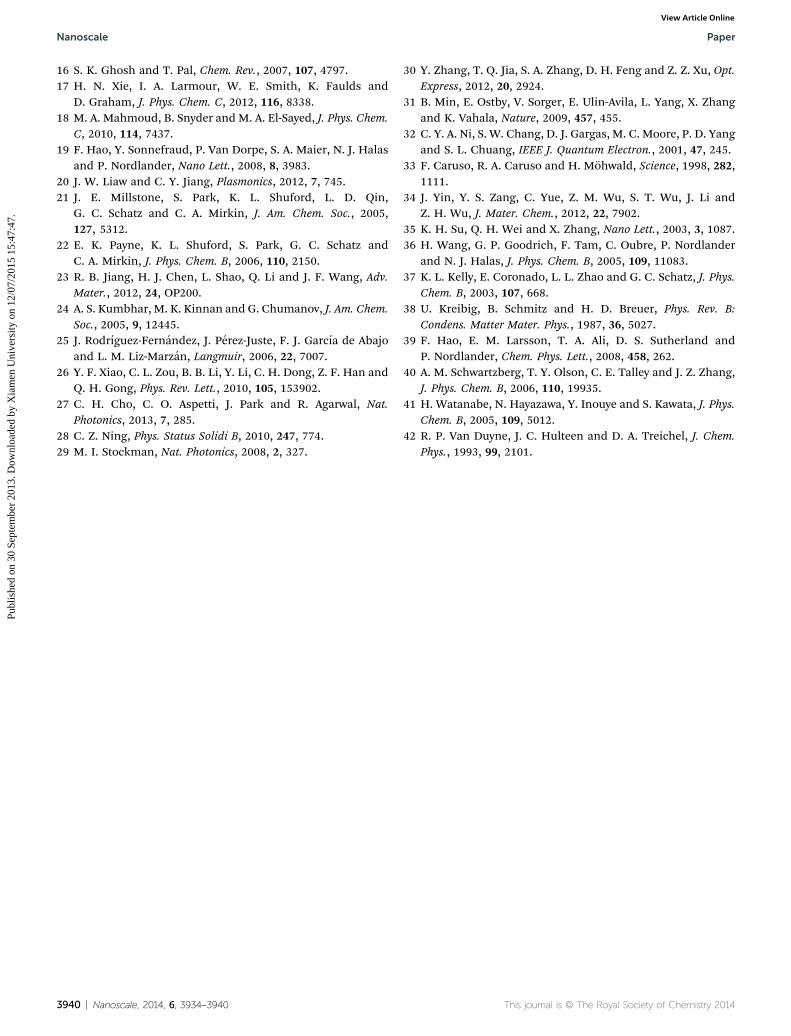
Fig. 7 (a) Raman mapping image on the Ag HNS arrays (10 mm � 10mm) at the Raman shift of 1360 cm�1, (b) the corresponding Ramanspectrum and (c) histogram of Raman intensities in the Ramanmapping of (a). All spectra in the considered region perform a back-ground subtraction before integration calculation.
Paper Nanoscale
Publ
ishe
d on
30
Sept
embe
r 20
13. D
ownl
oade
d by
Xia
men
Uni
vers
ity o
n 12
/07/
2015
15:
47:4
7.
View Article Online
largest enhancement is accomplished on the optimized Ag HNSarrays with a core diameter of 400 nm, which is consistent withthe calculation results as discussed above. Therefore, the AgHNS array is suitable as SERS substrates given its simplefabrication process and handy size and gap controlling.
In order to evaluate the SERS uniformity, Raman mappingwas performed on the fabricated Ag HNS arrays in a large area(10 mm � 10 mm) at the Raman shi of 1360 cm�1, as shown inFig. 7a. Each pixel in the confocal Raman mapping imagesrepresents the integral Raman intensity near 1360 cm�1 in thearea of interest (1320–1400 cm�1) as marked in Fig. 7b. Themapping image together with the histogram of Raman inten-sities shown in Fig. 7c demonstrates that uniform SERS signalscan be obtained on this self-assembled Ag HNS array substrate.
Conclusions
Multipole surface plasmon resonances: dipole, quadrupole,octupole and hexadecapole modes were observed in self-assembled metal hollow-nanosphere arrays and furtherdemonstrated by the extinction spectra and FDTD simulations.The highly localized near-eld on the surface of the Ag HNS
This journal is © The Royal Society of Chemistry 2014
arrays due to themultipole mode plasmonic resonances and theperiodic hot spots generated from the high order LSPR and itsinterparticle coupling effect make these metal nanostructurearrays a suitable SERS substrate for bio-sensing. In this manner,a sensitive SERS performance was accomplished on the Ag HNSarray substrate with optimized size and gaps. Further Ramanmapping characterization results on these metal HNS arrays ina large area evidently conrm that these periodic plasmonichollow cavity arrays could be used as a stable and uniform SERS-active substrate with wide applications in bio-sensing, analyt-ical chemistry and so on. Furthermore, broadband lightmanipulation, such as light trapping, from the UV to the near-infrared region can also be potentially achieved by using themultipole surface plasmon resonances in this metal hollowspherical structure.
Acknowledgements
This work is nancially supported by the MOST of China underthe 973 programs (2009CB930704), National Natural ScienceFoundation of China (61106118), Science and TechnologyProject of Fujian Province of China (2013H0046), NaturalScience Foundation of Fujian Province of China (2011J01362),and Fundamental Research Funds for the Central Universities(2011121026).
Notes and references
1 M. G. Albrecht and J. A. Creighton, J. Am. Chem. Soc., 1977,99, 5215.
2 S. M. Nie and S. R. Emory, Science, 1997, 275, 1102.3 K. Kneipp, Y. Wang, H. Kneipp, L. T. Perelman and I. Itzkan,Phys. Rev. Lett., 1997, 78, 1667.
4 H. R. Raether, Surface Plasmons on Smooth and RoughSurfaces and on Gratings, Springer, 1988.
5 N. J. Halas, S. Lal, W. S. Chang, S. Link and P. Nordlander,Chem. Rev., 2011, 111, 3913.
6 L. Shao, K. C. Woo, H. J. Chen, Z. Jin, J. F. Wang andH. Q. Lin, ACS Nano, 2010, 4, 3053.
7 M. Rycenga, X. Xia, C. H. Moran, F. Zhou, D. Qin, Z. Y. Li andY. Xia, Angew. Chem., Int. Ed., 2011, 50, 5473.
8 H. Wang, D. W. Brandl, P. Nordlander and N. J. Halas, Acc.Chem. Res., 2007, 40, 53.
9 S. Pattanayak, A. Priyam and P. Paik, Dalton Trans., 2013, 42,10597.
10 A. Priyam, N. M. Idrisa and Y. Zhang, J. Mater. Chem., 2012,22, 960.
11 E. Prodan, C. Radloff, N. J. Halas and P. Nordlander, Science,2003, 302, 419.
12 L. J. Sherry, S. H. Chang, G. C. Schatz, R. P. Van Duyne,B. J. Wiley and Y. N. Xia, Nano Lett., 2005, 5, 2034.
13 H. Minassian, K. Madoyan and A. Melikyan, Plasmonics,2012, 7, 745.
14 A. M. Schwartzberg, T. Y. Olson, C. E. Talley and J. Z. Zhang,J. Phys. Chem. B, 2006, 110, 19935.
15 A. M. Schwartzberg, T. Y. Oshiro, J. Z. Zhang, T. Huser andC. E. Talley, Anal. Chem., 2006, 78, 4732.
Nanoscale, 2014, 6, 3934–3940 | 3939
Nanoscale Paper
Publ
ishe
d on
30
Sept
embe
r 20
13. D
ownl
oade
d by
Xia
men
Uni
vers
ity o
n 12
/07/
2015
15:
47:4
7.
View Article Online
16 S. K. Ghosh and T. Pal, Chem. Rev., 2007, 107, 4797.17 H. N. Xie, I. A. Larmour, W. E. Smith, K. Faulds and
D. Graham, J. Phys. Chem. C, 2012, 116, 8338.18 M. A. Mahmoud, B. Snyder and M. A. El-Sayed, J. Phys. Chem.
C, 2010, 114, 7437.19 F. Hao, Y. Sonnefraud, P. Van Dorpe, S. A. Maier, N. J. Halas
and P. Nordlander, Nano Lett., 2008, 8, 3983.20 J. W. Liaw and C. Y. Jiang, Plasmonics, 2012, 7, 745.21 J. E. Millstone, S. Park, K. L. Shuford, L. D. Qin,
G. C. Schatz and C. A. Mirkin, J. Am. Chem. Soc., 2005,127, 5312.
22 E. K. Payne, K. L. Shuford, S. Park, G. C. Schatz andC. A. Mirkin, J. Phys. Chem. B, 2006, 110, 2150.
23 R. B. Jiang, H. J. Chen, L. Shao, Q. Li and J. F. Wang, Adv.Mater., 2012, 24, OP200.
24 A. S. Kumbhar, M. K. Kinnan and G. Chumanov, J. Am. Chem.Soc., 2005, 9, 12445.
25 J. Rodrıguez-Fernandez, J. Perez-Juste, F. J. Garcıa de Abajoand L. M. Liz-Marzan, Langmuir, 2006, 22, 7007.
26 Y. F. Xiao, C. L. Zou, B. B. Li, Y. Li, C. H. Dong, Z. F. Han andQ. H. Gong, Phys. Rev. Lett., 2010, 105, 153902.
27 C. H. Cho, C. O. Aspetti, J. Park and R. Agarwal, Nat.Photonics, 2013, 7, 285.
28 C. Z. Ning, Phys. Status Solidi B, 2010, 247, 774.29 M. I. Stockman, Nat. Photonics, 2008, 2, 327.
3940 | Nanoscale, 2014, 6, 3934–3940
30 Y. Zhang, T. Q. Jia, S. A. Zhang, D. H. Feng and Z. Z. Xu, Opt.Express, 2012, 20, 2924.
31 B. Min, E. Ostby, V. Sorger, E. Ulin-Avila, L. Yang, X. Zhangand K. Vahala, Nature, 2009, 457, 455.
32 C. Y. A. Ni, S. W. Chang, D. J. Gargas, M. C. Moore, P. D. Yangand S. L. Chuang, IEEE J. Quantum Electron., 2001, 47, 245.
33 F. Caruso, R. A. Caruso and H. Mohwald, Science, 1998, 282,1111.
34 J. Yin, Y. S. Zang, C. Yue, Z. M. Wu, S. T. Wu, J. Li andZ. H. Wu, J. Mater. Chem., 2012, 22, 7902.
35 K. H. Su, Q. H. Wei and X. Zhang, Nano Lett., 2003, 3, 1087.36 H. Wang, G. P. Goodrich, F. Tam, C. Oubre, P. Nordlander
and N. J. Halas, J. Phys. Chem. B, 2005, 109, 11083.37 K. L. Kelly, E. Coronado, L. L. Zhao and G. C. Schatz, J. Phys.
Chem. B, 2003, 107, 668.38 U. Kreibig, B. Schmitz and H. D. Breuer, Phys. Rev. B:
Condens. Matter Mater. Phys., 1987, 36, 5027.39 F. Hao, E. M. Larsson, T. A. Ali, D. S. Sutherland and
P. Nordlander, Chem. Phys. Lett., 2008, 458, 262.40 A. M. Schwartzberg, T. Y. Olson, C. E. Talley and J. Z. Zhang,
J. Phys. Chem. B, 2006, 110, 19935.41 H. Watanabe, N. Hayazawa, Y. Inouye and S. Kawata, J. Phys.
Chem. B, 2005, 109, 5012.42 R. P. Van Duyne, J. C. Hulteen and D. A. Treichel, J. Chem.
Phys., 1993, 99, 2101.
This journal is © The Royal Society of Chemistry 2014