multifunctional high performance van der waals … o ed. 1 supplementary information for...
TRANSCRIPT

In the format provided by the authors and unedited.
1
Supplementary information for
Multifunctional high performance van der Waals heterostructures
Mingqiang Huang, Shengman Li, Zhenfeng Zhang, Xiong Xiong, Xuefei Li and Yanqing Wu
Supplementary Information
S1: Additional electronic properties of VFET
S2: Electronic properties of HJFET
S3: Detailed IdVg curves for ternary inverter
S4. Tunable ternary inverter
S5. IdVg of in-series FET
S6: BP-MoS2 inverter with ultrahigh gain up to 152
S7: PVD encapsulation for heterostructure ternary inverter
S8: PVD encapsulation for binary inverters
S9: Temperature dependence of Heterojunction based ternary inverter
S10: Temperature dependence of In-series field effect transistor based ternary inverter
S11: Temperature dependence of In-series field effect transistor based binary inverter
S12: Multivalued logic
S13: Comparison of BP-MoS2 heterostructures with previous works
© 2017 Macmillan Publishers Limited, part of Springer Nature. All rights reserved.
SUPPLEMENTARY INFORMATIONDOI: 10.1038/NNANO.2017.208
NATURE NANOTECHNOLOGY | www.nature.com/naturenanotechnology 1
2
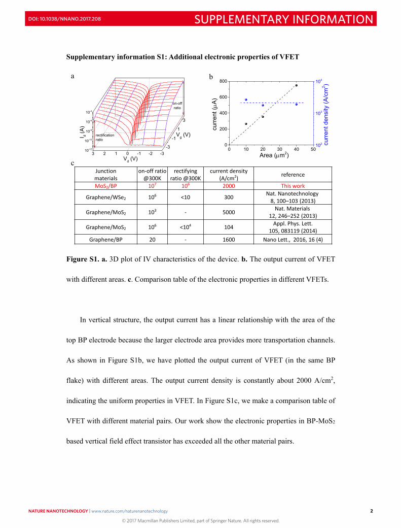
Supplementary information S1: Additional electronic properties of VFET
Junctionmaterials
on-off ratio@300K
rectifying ratio @300K
current density (A/cm2) reference
MoS2/BP 107 106 2000 This work
Graphene/WSe2 106 <10 300 Nat. Nanotechnology8, 100–103 (2013)
Graphene/MoS2 103 - 5000 Nat. Materials12, 246–252 (2013)
Graphene/MoS2 106 <104 104 Appl. Phys. Lett. 105, 083119 (2014)
Graphene/BP 20 - 1600 Nano Lett., 2016, 16 (4)
0 10 20 30 40 500
200
400
600
800
Area (m2)
curre
nt (
A)
102
103
104
curre
nt d
ensi
ty (A
/cm
2 )
ba
c3 2 1 0 -1 -2 -3
10-12
10-10
10-8
10-6
10-4
on-off ratio
rectificationratio
I d (A
)
3
1
-1Vg (V)
Vd (V)
-3
Figure S1. a. 3D plot of IV characteristics of the device. b. The output current of VFET
with different areas. c. Comparison table of the electronic properties in different VFETs.
In vertical structure, the output current has a linear relationship with the area of the
top BP electrode because the larger electrode area provides more transportation channels.
As shown in Figure S1b, we have plotted the output current of VFET (in the same BP
flake) with different areas. The output current density is constantly about 2000 A/cm2,
indicating the uniform properties in VFET. In Figure S1c, we make a comparison table of
VFET with different material pairs. Our work show the electronic properties in BP-MoS2
based vertical field effect transistor has exceeded all the other material pairs.
© 2017 Macmillan Publishers Limited, part of Springer Nature. All rights reserved.
NATURE NANOTECHNOLOGY | www.nature.com/naturenanotechnology 2
SUPPLEMENTARY INFORMATIONDOI: 10.1038/NNANO.2017.208
3
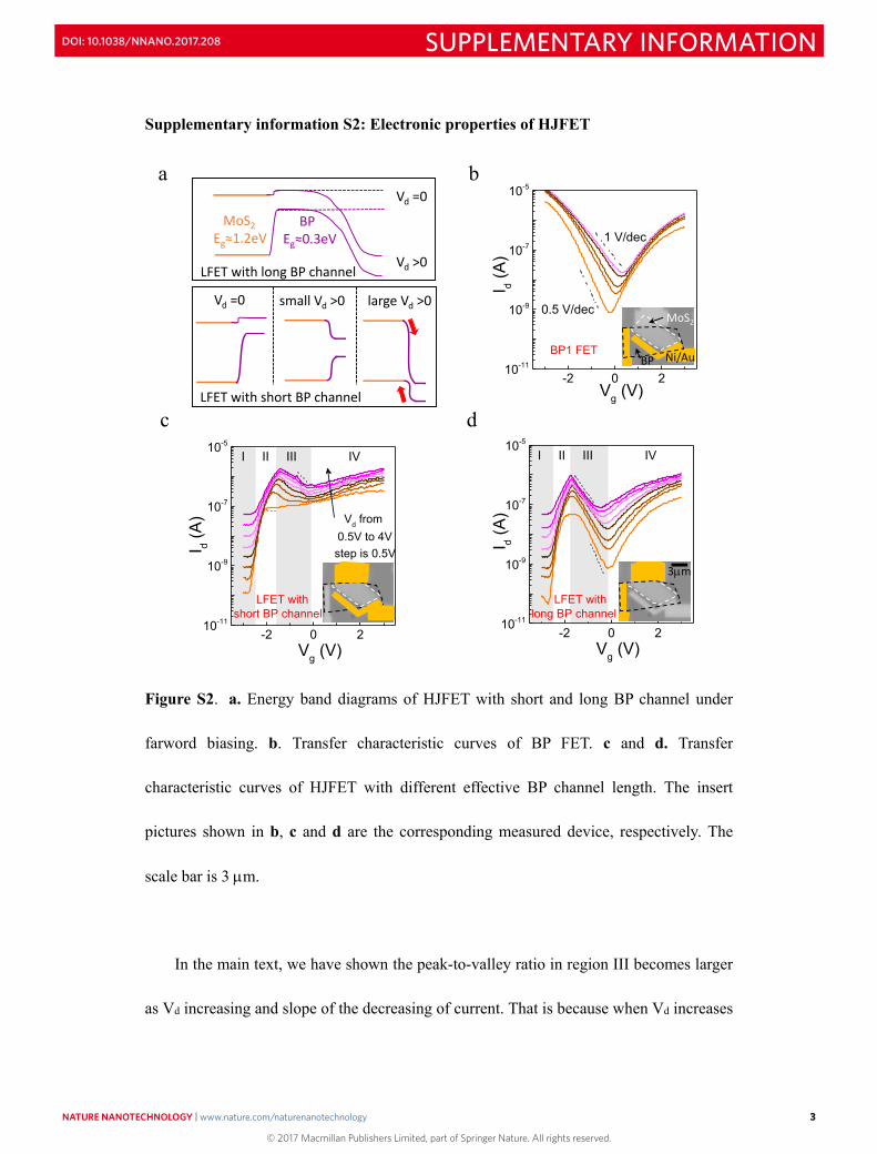
Supplementary information S2: Electronic properties of HJFET
-2 0 210-11
10-9
10-7
10-5
BP1 FET
1 V/dec
I d (A
)
Vg (V)
0.5 V/dec
a b
c d
-2 0 210-11
10-9
10-7
10-5
I II III IV
I d (A
)
Vg (V)
LFET withshort BP channel
Vd from0.5V to 4Vstep is 0.5V
-2 0 210-11
10-9
10-7
10-5
I d (A
)
Vg (V)
I II III IV
LFET withlong BP channel
Vd =0
Vd >0LFET with long BP channel
Vd =0 small Vd >0 large Vd >0
LFET with short BP channel
MoS2
BP Ni/Au
BPEg≈0.3eV
MoS2Eg≈1.2eV
3m
Figure S2. a. Energy band diagrams of HJFET with short and long BP channel under
farword biasing. b. Transfer characteristic curves of BP FET. c and d. Transfer
characteristic curves of HJFET with different effective BP channel length. The insert
pictures shown in b, c and d are the corresponding measured device, respectively. The
scale bar is 3 m.
In the main text, we have shown the peak-to-valley ratio in region III becomes larger
as Vd increasing and slope of the decreasing of current. That is because when Vd increases
© 2017 Macmillan Publishers Limited, part of Springer Nature. All rights reserved.
NATURE NANOTECHNOLOGY | www.nature.com/naturenanotechnology 3
SUPPLEMENTARY INFORMATIONDOI: 10.1038/NNANO.2017.208

4
further (about Vd = 1V), the valence band of BP is pulled down to be equal to the valence
band of MoS2, thus the barrier for holes decreases to zero and BP channel will dominate
the current transport. The larger the drain bias, the more effective the gate field controls
the channel where no internal barrier exists to block the carrier transport. However, it is
not always right especially when the effective BP channel is long enough. Figure S2c and
Figure S2d have shown two Id-Vg curves of HJFET with different BP channel length, in
which the drain voltage increases from 0.5 V to 4 V and the step is 0.5 V. In both HJFETs,
there exhibits four distinct regions in gate modulation but the peak-to-valley ratio in
region III becomes smaller in Figure S2b. This is because the BP channel is long enough
and the energy band will not be pull down easily as the short BP channel as shown in
Figure S2a. Thus the long BP channel will dominate the carrier transportation (see Figure
S2b and Figure S2d).
© 2017 Macmillan Publishers Limited, part of Springer Nature. All rights reserved.
NATURE NANOTECHNOLOGY | www.nature.com/naturenanotechnology 4
SUPPLEMENTARY INFORMATIONDOI: 10.1038/NNANO.2017.208

5
Supplementary information S3: Detailed IdVg curves for ternary inverter
-3 -2 -1 0 1 2 310-10
10-9
10-8
10-7
10-6
10-5
Vd from 0.2V to 2V
BP FET
I d (A
)
Vg (V)
LFET
Figure S3. Detailed IdVg curves for ternary inverter in main text Fig. 4.
As shown in Figure S2, there exists a longer parallel region III exists for the two
transfer characteristics curves (BP FET and HJFET) at large Vd and only one intersection
point at small Vd. The parallel Id-Vg in log scale means the resistance ratio of the pull-up
transistor and pull-down transistor is constant, thus the Vout-Vin curves will show a middle
logic state. It is important to note the Vd in supplementary information Figure S3 is not
equal to Vdd in Fig. 4 in the main text because the Vdd in an inverter equals to the sum of
voltage drops on both BP FET and the heterojunction, while the Id-Vg curves are
measured individually at a certain drain voltage.
© 2017 Macmillan Publishers Limited, part of Springer Nature. All rights reserved.
NATURE NANOTECHNOLOGY | www.nature.com/naturenanotechnology 5
SUPPLEMENTARY INFORMATIONDOI: 10.1038/NNANO.2017.208

6
Supplementary information S4. Tunable ternary inverter
-4 -3 -2 -1 00.0
0.2
0.4
0.6
0.8
1.0
Vin (V)
V out (
V)
0
2
4
6
8
logic 0
logic 1
Gainlogic 1/2
LBP2 = 0.5mLBP1 = 1.3m
Lch of MoS2 1m 3 m 5 m
-4 -3 -2 -1 00.0
0.2
0.4
0.6
0.8
1.0
Vin (V)
V out (
V)
logic 0
logic 1
mind-logic
0
3
6
9
12
15
LBP2 =2.5mLBP1 =1.3m
1m 3 m 5 m
Gain
Lch of MoS2
-4 -3 -2 -1 00.0
0.2
0.4
0.6
0.8
1.0
Vin (V)
V out (
V)
logic 0
logic 1
mid-logic
LBP2 = 1mLBP1 = 3m
Lch of MoS2 1m 3 m 5 m
0
2
4
6
8
Gain
a
c d
b
Vin
Vout
VddGNDUBP2MoS2 BP1
Figure S4. a: circuits diagrams of the ternary inverter. b, c, d: the channel length ratio of
LBP2/LBP1=0.33, 0.39, 1.9, respectively. And the output middle logic value decreases from
0.65Vdd to 0.2Vdd.
By combining BP FET and in-series FET, for the first time, we have successfully
demonstrated controllable ternary inverter that both the middle output value and middle
region length can be well tuned as shown in Figure S4. We have concluded that the output
middle region length is dominated by the MoS2 side that with a shorter channel length of
MoS2, the middle logic region length will be larger. And the output middle logic value is
dominated by the channel length ratio of LBP2/LBP1 that with a larger ratio, the output
middle logic value will be smaller.
© 2017 Macmillan Publishers Limited, part of Springer Nature. All rights reserved.
NATURE NANOTECHNOLOGY | www.nature.com/naturenanotechnology 6
SUPPLEMENTARY INFORMATIONDOI: 10.1038/NNANO.2017.208

7
Supplementary information S5. IdVg of in-series FET
-4 -3 -2 -1 0 1 2 3 410-12
10-10
10-8
10-6
10-4
I d (A
)
Vg (V)
0.1m 3m 5m
@Lch of MoS2 FET=3m
Lch of BP FET
-4 -3 -2 -1 0 1 2 3 410-12
10-10
10-8
10-6
10-4
I d (A
)
Vg (V)
0.1m 3m 5m
@Lch of BP FET=3m
Lch of MoS2 FET
a b
Figure S5. a: IdVg curves of the in-series FET, in which the channel length of BP is fixed
at Lch = 3 m, and the channel length of MoS2 changes from 0.1 to 5 m. b: IdVg curves
of the in-series FET, in which the channel length of MoS2 is fixed at Lch= 3 m.
The transfer characteristic curve of the in-series FET has been shown in Figure S5.
Similar to HJFET, there are also four regions in the Id-Vg curve, in which region II and III
are absolutely dominated by MoS2 FET and BP FET, respectively. The current of the
in-series FET in region IV is tunable by simply changing the channel length of BP.
However, the region I is always showing very small current from the depleted MoS2 and
thus it cannot form MoS2 FET and in-series FET based ternary inverter.
© 2017 Macmillan Publishers Limited, part of Springer Nature. All rights reserved.
NATURE NANOTECHNOLOGY | www.nature.com/naturenanotechnology 7
SUPPLEMENTARY INFORMATIONDOI: 10.1038/NNANO.2017.208

8
Supplementary information S6: BP-MoS2 inverter with ultrahigh gain over 150.
-0.5 0.0 0.5 1.00.0
0.5
1.0
1.5
2.0
2.5
3.0
Vin (V)
Vou
t (V
)
200
150
100
50
0
Gai
n
Gain = 152
Figure S6. Vout-Vin plots and voltage gain of the inverter.
In the main text, we have introduced the channel length engineering to enlarge the
voltage gain of BP-MoS2 based binary inverter, which is extremely effective to gain
well-matched threshold voltage of MoS2 FET and BP FET. Further, we have fabricated
several such binary inverter with similar structure. Most of the devices can show a high
gain larger than 60. And the highest is 152 (figure S6), which is the largest gain among all
the 2D based inverters.
© 2017 Macmillan Publishers Limited, part of Springer Nature. All rights reserved.
NATURE NANOTECHNOLOGY | www.nature.com/naturenanotechnology 8
SUPPLEMENTARY INFORMATIONDOI: 10.1038/NNANO.2017.208

9
Supplementary information S7: PVD encapsulation for heterostructure ternary
inverter
0 1 2 3 40
2
4
6
8
10
Gai
n
Time (weeks)
the second gain the first gain
0
4
8
12
16
secondgain
first gain
device 2
before encapsulation after encapsulation
Gai
n
secondgain
device 1
first gain
secondgain
device 3
first gain
-2 -1 0 1 20.0
0.5
1.0
1.5
2.0
Vou
t (V
)
Vin (V)-3 -2 -1 0 1
0.0
0.5
1.0
1.5
2.0
Vou
t (V
)
Vin (V)
before encapsulation after encapsulationa. b.
c. d.
Figure S7. a and b: Performance of heterostructures based ternary inverter before and
after Al2O3 encapsulation, respectively. c: Voltage gain of the three devices. d: air stability
of the device.
Figure S7a and S7b show the performance of heterostructures based ternary inverter
before and after Al2O3 encapsulation, respectively. The device performance shows no
degradation, instead small improvement after encapsulation, and both show well-shape
Vout-Vin plots with distinguishing logic 1, logic 1/2 and logic 0. To make a systematic
comparison, three similar BP/MoS2 heterostructure devices have been fabricated side by
side, and all devices show similar results. The voltage gain of the three devices at Vdd
© 2017 Macmillan Publishers Limited, part of Springer Nature. All rights reserved.
NATURE NANOTECHNOLOGY | www.nature.com/naturenanotechnology 9
SUPPLEMENTARY INFORMATIONDOI: 10.1038/NNANO.2017.208
10
=2.5V have been summarized in Fig. S7c, where the red histogram represents the gain
before encapsulation and the blue one is after encapsulation. The two gains from the
ternary inverter have been improved after encapsulation for all three devices. After
encapsulations, these devices are always placed in ambient conditions and detailed DC
measurements has been carried out every week. As is shown in Fig. S7d, the two voltage
gains of a representative device (corresponding to device2) at Vdd = 2 V show no
degradation up to 4 weeks. Such significantly improved air stability demonstrates great
potential for BP electronic devices.
© 2017 Macmillan Publishers Limited, part of Springer Nature. All rights reserved.
NATURE NANOTECHNOLOGY | www.nature.com/naturenanotechnology 10
SUPPLEMENTARY INFORMATIONDOI: 10.1038/NNANO.2017.208

11
Supplementary information S8: PVD encapsulation for binary inverters
The encapsulation of in-series BP/MoS2 field effect transistor based inverter has also
been systematically studied. The device was firstly encapsulated by PVD methods with 3
nm Al seeding layers. Then detailed DC measurements has been carried out every other
week after two weeks, during which the device is always kept in ambient conditions.
0 2 4 6 8
0
10
20
30
Gai
n
Time (weeks)
a. b.
-1.0 -0.5 0.0 0.5 1.00.0
0.5
1.0
1.5
2.0
time of device placedin ambient conditions
1 week 2 weeks 4 weeks 6 weeks 8 weeks
Vou
t (V
)
Vin (V)
Figure S8. a Vout-Vin plot of the device at different weeks after Al2O3 encapsulation. b:
air stability of the device.
Fig. S8a shows the Vout-Vin curves of the encapsulated inverter under ambient
conditions for different duration of time. The data show slight shift and reach stable
conditions after 4 weeks after encapsulation. The voltage gain (fig. S8b) shows
continuous increasing until 4 weeks and stays at same values thereafter. It is noted that the
gain increase from around 10 for the original device to 32 after encapsulation at Vdd = 2
V.
© 2017 Macmillan Publishers Limited, part of Springer Nature. All rights reserved.
NATURE NANOTECHNOLOGY | www.nature.com/naturenanotechnology 11
SUPPLEMENTARY INFORMATIONDOI: 10.1038/NNANO.2017.208

12
Supplementary information S9: Temperature dependence of Heterojunction based
ternary inverter
-2 -1 0 1 20.0
0.5
1.0
1.5
2.0
2.5
from room temperature down to 20K
Vou
t (V
)
Vin (V)
0 100 200 3000
10
20
30
40
50 Device 1
the first gain
the second gainGai
n
Temperature (K)
a. b.
0 100 200 300
0
4
8
12
16 Device 3
Gai
n
Temperature (K)0 100 200 300
0
5
10
15
20
25
30
35 Device 2
Gai
n
Temperature (K)
-2 -1 0 1 20
10
20
30
40
Gai
n
Vin (V)
300 280 260 240 220 200 150 70 20
T (K)
c.
Figure S9. a and b: Performance of heterostructures based ternary inverter at different
temperature. c: Voltage gain of the three devices at different temperature.
The two voltage gains in heterojunction based ternary inverter are dominated by the
threshold voltage matching and the BP2 FET subthreshold swing, respectively. Under low
temperature, the on/off ratio of BP FET will be larger and the subthreshold swing (SS)
will be smaller. Thus the second voltage gain is predicted to be increasing, while the first
gain is predicted to show little variation. Fig. S9a has shown the Vout-Vin curve of the
ternary inverter (corresponding to device 2) at different temperature. While the inverter
shows slight transition voltage shift, the second voltage gain is continuous increasing
© 2017 Macmillan Publishers Limited, part of Springer Nature. All rights reserved.
NATURE NANOTECHNOLOGY | www.nature.com/naturenanotechnology 12
SUPPLEMENTARY INFORMATIONDOI: 10.1038/NNANO.2017.208

13
when temperature at lower temperatures as shown in Fig. S9b. The three new fabricated
BP/MoS2 heterostructure devices show similar results. We have summarized the two
gains of the three devices under different temperature in Fig. S9c. Particular for the
device 1, the second gain exhibits a 10x increase from around 5 at room temperature to 44
at T = 4.3 K, which can be attributed to the improved mobility and on-off properties.
© 2017 Macmillan Publishers Limited, part of Springer Nature. All rights reserved.
NATURE NANOTECHNOLOGY | www.nature.com/naturenanotechnology 13
SUPPLEMENTARY INFORMATIONDOI: 10.1038/NNANO.2017.208

14
Supplementary information S10: Temperature dependence of In-series field effect
transistor based ternary inverter
0 100 200 3000
2
4
6
8
10
12
the second gain the first gain
Gai
n
Temperature (K)-1.5 -1.0 -0.5 0.0 0.5
0.0
0.5
1.0
1.5
2.0T = 20 K
Vou
t (V
)
Vin (V)-3.0 -2.5 -2.0 -1.5 -1.0 -0.5 0.0
0.0
0.5
1.0
1.5
2.0
Vou
t (V
)
Vin (V)
T = 300 K
a. b. c.
Figure S10. a and b: The in-series field effect transistor based ternary inverter under
300K and 20K, respectively. c: Gain of the device under different temperature.
The in-series field effect transistor based ternary inverter under both high and low
temperature measurements have been carried out as shown in Fig. S10a and S10b, where
the temperature is 300K and 20K, respectively. Several revealing trends are evident in the
temperature-dependent data. First, the Vout-Vin curve shows continuous right shifting as
temperature decreasing down (The similar behavior can also be seen the heterojunction
device shown in Fig.S9a), especially at the transition region from middle-logic to logic 0.
This is generally because of the threshold voltage shifting of BP FET at low temperature.
Unintentional, this caused the middle-logic length become longer at low temperature
(Indeed, the similar behavior can be seen the heterojunction device as shown in Fig.S9a).
Secondly, the logic 0 becomes closer to real 0 at low temperature. This is because the
high on/off ratio and low off-state current of BP FET at T = 20 K, thus the relative
resistance of the pull-down transistor is small enough such that the logic low levels are
© 2017 Macmillan Publishers Limited, part of Springer Nature. All rights reserved.
NATURE NANOTECHNOLOGY | www.nature.com/naturenanotechnology 14
SUPPLEMENTARY INFORMATIONDOI: 10.1038/NNANO.2017.208

15
almost equal to GND. Finally, as shown in Fig. S10c, the first gain shows little variation
meanwhile the second gain is continuous increasing from 300K to 20K.
© 2017 Macmillan Publishers Limited, part of Springer Nature. All rights reserved.
NATURE NANOTECHNOLOGY | www.nature.com/naturenanotechnology 15
SUPPLEMENTARY INFORMATIONDOI: 10.1038/NNANO.2017.208

16
Supplementary information S11: Temperature dependence of In-series field effect
transistor based binary inverter
-1.0 -0.5 0.0 0.5 1.0
0.5
1.0
1.5
2.0
Vou
t (V
)
Vin (V)
from 300 Kdown to 20 K
0 100 200 3000
10
20
30
40
50
Gai
n
Temperature (K)
a. b.
-1.0 -0.5 0.0 0.5 1.00
10
20
30
40
50
300 280 260 240 220 200 180 150 110 70 20
Gai
n
Vin (V)
Temperature (K)
@Vdd = 2 Vc.
Figure S11. In-series BP MoS2 FET based binary inverter at different temperature
Under low temperature, the on/off ratio of both BP FET and MoS2 FET will be larger
and the subthreshold swing (SS) will be smaller. Thus the voltage gain is predicted to be
increasing. Fig. S11a and S11b have shown the Vout-Vin curve and the voltage gain of the
binary inverter at different temperature, respectively. As expected, the gain is continuous
increasing as temperature decreasing down. At T = 20 K, high gain of G = 47 at Vdd = 2 V
has been successfully reached (Fig. S11c).
© 2017 Macmillan Publishers Limited, part of Springer Nature. All rights reserved.
NATURE NANOTECHNOLOGY | www.nature.com/naturenanotechnology 16
SUPPLEMENTARY INFORMATIONDOI: 10.1038/NNANO.2017.208

17
Supplementary information S12: Multivalued logic
In the effort to increase the bit density, the fundamental limit of the current binary
system is that the number of bits cannot exceed the number of gates in the standard
two-valued Boolean logic gates. Multivalued logic such as a basic building block of
three-valued logic was considered as promising architectures to break the fundamental bit
limit. In the past decades, multivalued logic (MVL) has been studied for the purpose that
it has the potential for more logic states in smaller area and it also has the potential
application on augmentation of Binary Systems, Memory, Signaling and Arithmetic1.
So far, significant development has been achieved in the theory and design of
ternary-based arithmetic operations. A modest breakthrough in this aspect of MVL is
CMOS which consists of one PMOSFET, resistor_1, resistor_2 and one NMOSFET,
making it well-suited to ternary logic applications. Here, each CMOS enhancement
device acts as a reasonably ideal binary switch with a threshold which ensures that with
Vin high, PMOS is off while NMOS is on; with Vin low, PMOS is on while NMOS is off;
with Vin in the middle, both are on. With both devices on the middle input state, the
centrally connected output is also in the middle.
Many other methods have also been proposed to generate multivalued logic. Such as
charge mode, current mode, and voltage mode. To generate a new logic state, most
approaches require increasing the device integration complexity. For example, a ternary
NMOS high and low threshold detector need 6 NFETs. An NMOS ternary quantizing max
gate needs more than 10 FETs. How to simplify the device structure and reduce the
© 2017 Macmillan Publishers Limited, part of Springer Nature. All rights reserved.
NATURE NANOTECHNOLOGY | www.nature.com/naturenanotechnology 17
SUPPLEMENTARY INFORMATIONDOI: 10.1038/NNANO.2017.208

18
system interconnection is still a challenge which limits any real applications using this
architecture.
While in our ternary inverter design (Fig. 4a in the main text), there are only 2
transistors with 4 electrodes as in those standard binary inverters. We used similar area
and complexity to realize one more logic state than conventional transistors and 3n is
much larger than 2n especially when n gets very large. For the structure Fig. 5a in the
main text, as the reviewer correctly pointed out, there are 3 transistors involved to realize
a ternary function. It may seem unnecessarily complicated, however in principle, it has
the potential of realizing more logic states than conventional binary inverters in large
scale integration by reducing the interconnection and unit functionality. Moreover, in Fig.
5a in main text, the width of the ternary window can be tuned in a wide range by
matching of channel length, which will add additional degree of freedom for complex
functionality. In summary, we agree with the reviewer that the three transistors in Fig. 5a
in main text may seem to add unnecessary complicity, but meanwhile it brings new
potential functionalities in many potential applications.
© 2017 Macmillan Publishers Limited, part of Springer Nature. All rights reserved.
NATURE NANOTECHNOLOGY | www.nature.com/naturenanotechnology 18
SUPPLEMENTARY INFORMATIONDOI: 10.1038/NNANO.2017.208

19
Supplementary information S13: Comparison of BP-MoS2 heterostructures with
previous references
Table 1. Comparison of BP-MoS2 heterostructures with previous works
This work ref.2 ref.3 ref.4
materials CVD MoS2BP flake
CVD MoS2BP flake flake flake
device structure Vertical heterojunction
Lateralheterojunction
Lateralheterojunction
Lateralheterojunction
carrier injection length from electrode tens of nm ∼1 m > 10 m > 5 m
highlight point high rectification ratioand high on/off ratio
Photovoltaic effect
Photovoltaic effect
Photovoltaic effect
T = 300Krectification
ratio ∼106 ∼105 1000 143
on/off ratio 107 NA NA NA
T = 20Krectification
ratio ∼106 NA NA NA
on/off ratio ∼107 NA NA NA
Table 2. Comparison of BP-MoS2 inverter with previous work
this work ref.5
device structure BP-MoS2
HJFETBP-MoS2
in-series FETBP-MoS2
in-series FETBP-MoS2
in-series FETmulti value ternary ternary binary binary
tunabilityfrom binary to ternary logic
(by Vdd)
middle logic window (by Lch)
Vth matching by Lch
NA
before encapsulation T = 300K(first gain & second gain) 4 & 8 5 & 4 22
(best match 70) 3.5
before encapsulation T= 20K(first gain & second gain) 5 & 44 5 & 12 47 NA
after encapsulation T = 300K Yes Yes Yes NA
after encapsulation T= 20K Yes Yes Yes NA
air stability > 4 weeks > 8 weeks > 8 weeks NA
© 2017 Macmillan Publishers Limited, part of Springer Nature. All rights reserved.
NATURE NANOTECHNOLOGY | www.nature.com/naturenanotechnology 19
SUPPLEMENTARY INFORMATIONDOI: 10.1038/NNANO.2017.208

20
Reference
[1] Smith, Kenneth C. The prospects for multivalued logic: A technology and applications view. IEEE Trans. Computers 30.9 (1981): 619-634. [2] Deng, Y. et al. Black phosphorus-monolayer MoS2 van der Waals heterojunction p-n diode. Acs Nano 8, 8292-8299 (2014). [3] Ye, L., Li, H., Chen, Z. & Xu, J. Near-Infrared Photodetector Based on MoS2/Black Phosphorus Heterojunction. ACS Photonics 3 (4), 692–699 (2016). [4] Chen, Peng, et al. Gate tunable MoS2–black phosphorus heterojunction devices. 2D Materials 2.3: 034009 (2015) [5] Su, Y., Kshirsagar, C. U., Robbins, M. C., Haratipour, N. & Koester, S. J. Symmetric Complementary Logic Inverter Using Integrated Black Phosphorus and MoS2 Transistors. 2d Materials 3, 011006 (2015).
© 2017 Macmillan Publishers Limited, part of Springer Nature. All rights reserved.
NATURE NANOTECHNOLOGY | www.nature.com/naturenanotechnology 20
SUPPLEMENTARY INFORMATIONDOI: 10.1038/NNANO.2017.208