multi-layer system-on-substrate for ka-band foreign … · multi-layer system-on-substrate for...
TRANSCRIPT

Multi-layer System-on-Substrate for Ka-band Foreign Object Debris (FOD) Detection Sensor
GHULAM MEHDI, JUNGANG MIAO
School of Electronics & Information Engineering Beihang University
37 Xueyuan Road, Haidian District, Beijing CHINA
Abstract: - Presence of Foreign object debris (FOD) at airport runways is an immense threat to flight safety. Such objects may cause potential damage to the aircraft especially during the take off and landing. This paper introduces the design of a low-cost Ka-band FOD radar sensor adopting state-of-the-art system-on-substrate (SoS) approach. Contrary to the reported single-layer SoS design approach, multi-layer SoS configuration is introduced. The frequency modulated continuous-wave (FMCW) front-end transceiver and the integrated transmit and receive antennas are realized in multi-layer configuration. The front-end transceiver is mainly designed employing substrate integrated waveguide (SIW) circuits on low-cost 12 mil thick R4003C substrate. The front-end transceiver comprises of MMICs and passive structures such as SIW band-pass filters, SIW Wilkinson power divider and SIW-to-microstrip transitions. The antenna is of SIW traveling-wave slot array (TWSA) type realized on 60 mil thick R4003C. Unlike conventional coaxial matched loads used in SIW-TWSA, a virtually grounded resistive matched load is introduced for termination of such antenna in SIW technology. The simulation results of the proposed antenna and transceiver front-end are presented.
Key-Words: - Foreign object debris, system-on-substrate, substrate integrated waveguide, frequency modulated continuous-wave, slot array antenna 1 Introduction Foreign object debris (FOD) is an unwanted object found at the airport runways. Presence of FOD on airport runways is an immense threat to flight operation safety. Such unwanted objects may cause potential damage to the aircraft during critical phases like take off and landing. Federal aviation Administration (FAA) has released advisory circular providing information for FOD detection equipment [1]. FOD has always been remained a concern for safe flight operation. FOD detection has emerged as a motivating research area and gained significant attention after the accident of Concorde airplane in year 2000. In this accident, the tyre of the plane was cut by a metal strip lying on the runway. Due to the miniaturized nature of FOD parts, a very high resolution sensor is desired to resolve and locate such objects with higher degree of accuracy. Concurrently, the detection of very small radar cross section (RCS) of these FOD objects put stringent requirement on radar receiver (Rx) for high dynamic range typically 100 dB. The key challenges in the design of FOD radar sensor are extremely short range and cross-range resolution, detection of very small RCS objects in clutter environment and all weather day & night operation capability.
Additionally, such sensors have short detection range due to small FOD RCS and low transmit power levels employing solid state devices at millimeter-wave (mmW) bands. Usually, multiple sensors are deployed along the runway to provide complete lateral coverage. FMCW technique is suitable for FOD application because of its simplicity with fewer components and ability to provide very high range resolution while transmitting very low peak power. However the inherent issues associated with FMCW systems such as mutual coupling between transmit and receive antennae, self-mixing due to substrate coupling and flicker noise due to zero IF architecture of the Rx makes the design demanding [2]. Most of the reported FOD systems developed at W-band (75-110 GHz) exhibits fine angular resolution such as 0.5 m at short range distance of 150 m [3]–[5]. However, most of these systems are under the development and evaluation phase. In this work, design of a Ka-band FOD sensor is proposed introducing state-of-the-art multi-layer system-on-substrate (SoS) approach. The primarily objective is to realize a low-cost, miniaturized and portable radar sensor for FOD detection. The presented FMCW sensor design operates at Ka band (26.5-27
WSEAS TRANSACTIONS on CIRCUITS and SYSTEMS Ghulam Mehdi, Jungang Miao
E-ISSN: 2224-266X 31 Volume 14, 2015
GHz). In order to validate the concept, a relatively smaller 8x8 antenna array is designed. The array size can be extended for higher gain and narrow beamwidth later on.
The rest of the paper is arranged as follows. Section II presents an overview of substrate integrated waveguide (SIW) technology and SoS concept. Section III discusses the top level design of the proposed FOD sensor. A brief description and simulation results of a novel travelling-wave type slot array antenna realized in SIW technology is presented in section IV. Afterwards, the layout implementation of the FMCW transceiver is given in section V. Finally, the work is concluded in section VI. 2 Technology Overview 2.1 SIW Technology Lately, with the advent of substrate integrated waveguide (SIW) technology, it is now possible to realize the waveguide structures on laminated substrates. The conventional metallic waveguide components are bulky, expensive and require transitions to interface such components with planar circuits. However, they offer attractive features such as low loss and high Q factor. In SIW, the dielectric-filled laminated waveguide is bored with array of closely spaced metallic vias fence. This array of vias acts as a lateral wall. The promising advantages of such kind of waveguide are ease of integration with planar structures, reduced size, light weight, low profile and low cost. SIW components can be fabricated with the existing printed circuits techniques such as photolithographic printed circuit process, laser structuring, low temperature co-fired ceramic (LTCC) technique etc. The SIW can be constructed with any available substrate; however, low loss materials are preferred for high performance [6]. The SIW together with other types of synthesized waveguide can be generalized by a new concept called substrate integrated circuits (SIC) or often named as System-on-Substrate (SoS) that allows the integration of planar and non-planar structures within the same substrate. SIW is a structure integrated in planar form and is similar to conventional rectangular waveguide. The SIW can be synthesized and realized by employing two rows of metallic in the laminated dielectric substrate. In the design of SIW, the radius “r” of the vias, the center-to-center spacing between the vias “S” and the spacing between the two vias rows “a” are the design parameters. The leakage can be minimized
by selecting appropriate values of these parameters. For the given diameter (2r), pitch(S) and width (a), SIW channel can be approximated to its equivalent rectangular waveguide using expression (1) [6]:
( )222
0.95= − −eqv
ra a r
S (1)
2.2 System-on-substrate (SoS) Traditionally, mmW front-end modules are realized in planar form by employing microtstrip or CPW lines integrated with MMIC devices. This kind of MCM is further integrated with transmit and receive antennas which are usually non-planar such as parabolic dish, horn, waveguide slot array etc. The integration between the front-end and the antennas is accomplished by means of some transition such as waveguide/coaxial-to-microstrip. However, systems with such transitions are bulky and expensive. Additionally, the overall performance of the mmW system is also affected due to the transition losses. The emerging mmW commercial applications such as video transmission systems, security systems, broadband wireless, automotive radar, wearable sensors for body area networks etc necessitates ultra-miniaturized and low cost solutions [7].
In order to circumvent the problems associated with the conventional method, a promising alternative is system-on-substrate (SoS) approach. The SoS is a technology concept where a complete radio system or sub-system is realized on a single substrate and usually packaged in a single module. In order to obtain high performance and realize a highly miniaturized system, usually, microwave & mmW system designers prefer to embed the antenna system with RF front-end in a single package. Thus, the front-end system and antenna system together are realized on a single employing substrate integrated circuits (SIC). The integrated mmW radio systems realized on multi-layer substrates adopting SoS approach is analogous to a system-in-package (SiP). This emerging technology enables the designer to realize complete mmW front-end with integrated antenna. SoS design methodology is best suitable for realizing extremely compact, high performance and low-cost mmW systems. Lately, substrate integrated waveguide (SIW) has gained considerable attention as a low-loss alternative to microstrip, CPW lines and conventional rectangular waveguides. The SICs realized in SIW technology can be integrated transitions to conventional planar transmission lines by means of transitions. The SIW technology is being widely used for various practical microwave and mmW components. SIW
a
WSEAS TRANSACTIONS on CIRCUITS and SYSTEMS Ghulam Mehdi, Jungang Miao
E-ISSN: 2224-266X 32 Volume 14, 2015

allows the realization of components ranging from simple transitions to large size slot array antennas. A 60-GHz MCM Rx employing SIW filter and antenna is presented in [8]. The Rx is integrated onto a single multilayer substrate, fabricated using photo-imageable thick-film technology. An integrated FMCW radar front-end based on SoS concept is presented in [7] with all blocks realized on a single substrate. An integrated 60-GHz switched beam smart antenna subsystem is demonstrated on almost all 60-GHz SIW components including a slot antenna, 4x4 Butler matrix network, band-pass filter, sub-harmonically pumped mixer, and local oscillator (LO) source [8]. However, these mmW SoS systems and sub-systems adopting SoS are realized on a single-layer substrate occupying relatively larger space. Additionally, mmW antenna and front-end are stacked on the same surface over the substrate. over the same substrate may effect the performance of antenna radiation pattern as well as performance of front-end sub-system. For instance, for large signal power levels, the currents and fields are established over the substrate surface. This possibly large time-varying signal superimposed on the DC bias lines may interrupt the linear and specially tuneable non-linear devices in the system [9]. Contrary to single-substrate SoS design approach, multi-substrate SoS configuration is introduced. The proposed approach addresses the problems associated with the single substrate SoS approach resulting high performance and ultra-miniaturized mmW systems. The possible technologies for multi-layer SoS fabrication include low-temperature co-fired ceramics (LTCC), thin/thick film on glass. For economical solution, low-cost commercially available laminated substrates may be opted rather than going for other expensive solutions such as thin film or LTCC processes. 3 Top Level Design Firstly, the general specifications of the radar are outlined. Later, the key radar characteristics such as detection range, sensitivity, range resolution etc are computed. Consequently, the block diagram of the prototype FMCW sensor is illustrated. The sensor design is modeled in ADS® and validated though system level simulations. The preliminary design is aimed for detection of FOD objects up to 100 meters range with a positioning accuracy of 1 meter. Rdar cross-section (RCS) of such objects is typically from -20dBm to -25 dBsm. The selection of radar operating frequency band 26.5-27 GHz at Ka-band arises from the considerations such as inherent advantages of mmW for imaging sensors,
availability of commercial MMICs and frequency authorization for radar sensors. In the design of FMCW radar systems, the two key parameters are the frequency deviation (∆ƒ) and modulating signal (fm) The required range resolution (R.R.) is 0.3 m, therefore, ∆ƒ can be calculated using (2)
. .2.
=∆CR R
f (2)
Thus, the required f∆ is 500 MHz. The resolution in frequency domain is 1/Tm. The sawtooth modulating signal fm (where fm=1/Tm) is selected instead of triangular signal. This is due to the fact the sensor is primarily meant for detection of stationary targets and doppler processing is not intended. Tm of 1 mSec is chosen based on considerations. For ∆ƒ of 500 MHz, Tm of 1 mSec is a suitable value and corresponds to maximum beat frequency lower than 1 MHz at 100 meters of range [10]. The design rests on the initial known parameters. The carrier frequency, FOD RCS, Tx/Rx antenna gain, maximum range, and transmit power are 26.75 GHz, -25 dBsm, 20 dBi, 100 m and 20 dBm respectively. Received power can be calculated from expression (3) [29]:
( )
2 2
3 44λ σ
π= t
rPGP
R (3)
The minimum received signal Pr,min at maximum range of 100 meter comes out to be -117 dBm. Based on the selection of MMICs, the Rx noise figure is approximated to be 3 dB. The minimum detectable signal (MDS) on the receiver (Rx) side can be expressed as [11]:
min174 10log( )= − + + +total FFTMDS NF BW SNR (4) In radar systems, typically SNR value of 15 dB ensures probability of detection of 95% and the FFT bandwidth is 1 KHz. Thus, the MDS comes out to be -120 dBm. Since MDS is lower than Pr,min, the sensitivity of the Rx is adequate for detection of -25 dBm RCS targets at ranges up to 100 meters. Alternatively, SNR at the maximum range can be computed using (5) [12], Where LS (system losses),GR (antenna gain), fm and PCW are 3dB, 20dB, 1 KHz and 20dBm respectively.
( )
142
max 34 . . . . .λ σ
π
=
cw T R T
m s out
P G GRK T NF f L SNR
(5)
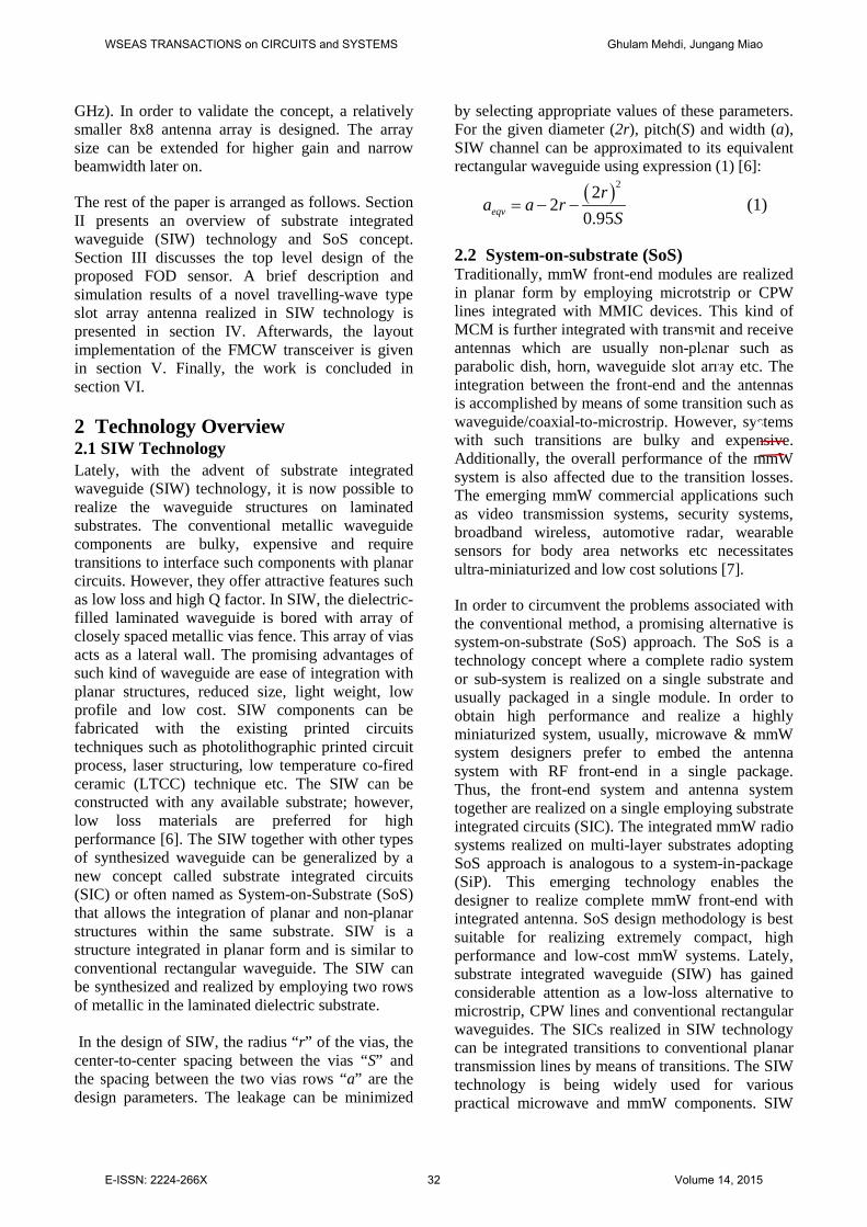
The block diagram of the FMCW transceiver is illustrated in Fig.1 of the appendix at the end. The direct digital synthesizer (DDS) generates the linear frequency modulated (LFM) chirp and later up-converted to 6.625 GHz inside the synthesizer unit. The chirp signal is filtered before it is fed to the
WSEAS TRANSACTIONS on CIRCUITS and SYSTEMS Ghulam Mehdi, Jungang Miao
E-ISSN: 2224-266X 33 Volume 14, 2015

front-end MCM. The Rx configuration is single stage homodyne (zero IF). Commercially available MMICs are employed for the transceiver front-end while passive structures are designed in SIW technology. The detailed layout design implementation of the front-end transceiver is discussed in section V. Transmit (Tx) unit comprises of two frequency multipliers and their corresponding harmonic suppression BPFs used to convert the signal frequency from 6.625 GHz to 26.5 GHz. The detection and ranging accuracy of a FMCW system depends on the phase noise of the VCO and linearity of the chirp signal respectively. The first active doubler translates 6.625 GHz to 13.25 GHz. A SIW BPF follows the first multiplier. The second multiplier translates the 13.25 GHz to 26.5 GHz signal. A SIW BPF centered at 26.5 GHz is incorporated for suppression of unwanted harmonics. In order to obtain the total frequency deviation of 500 MHz, the DDS frequency deviation is programmed to 125 MHz. This bandwidth is multiplied four times by the two frequency multiplier stages resulting in a total bandwidth of 500 MHz [13]. Finally, the output of second multiplier is divided into two halved power signals. This is accomplished by employed a SIW Wilkinson power divider. One signal is applied to the LO port Rx unit while the other signal line is fed to the power amplifier. The substrate integrated circuits are designed and simulated in Ansoft HFSS® and the detailed description is given in section V. In order to analyze the sensor’s detection performance, a simulation model of the radar transceiver is developed in ADS®. The simulated targets are generated by introducing appropriate attenuations and time delays corresponding to the power levels and ranges of the respective targets. The results show that, with 20 dBm of transmit power, the system is capable of detecting small FOD objects (-25 dBsm RCS) at ranges up to 100 meter. Since the radar azimuth beamwidth is large, the concept of multi-radars network shall be employed for improved positioning accuracy [14]. 4 FOD Antenna Usually, radar sensors are installed with narrow beam, wide bandwidth and high gain antennas for fine lateral resolution, high range resolution and longer detection ranges respectively. The FOD sensor reported in [15] operates at 78 GHz frequency and a planar folded reflectarray antenna has been employed in the sensor. The diameter of
the antenna is 130 mm and the measured gain is 35 dBi. The antenna assembly in [16] adopts a particular configuration similar to a lighthouse, i.e. a fixed feeder and the reflector rotating around. The pulsed sensor operates at 95 GHz. In [4], standard gain horn antenna are used for transmit and receive operation. All of these antennas are integrated with the rest of the system hardware by means of non planar transitions which makes these systems bulky and expensive. A compact, light weight and low cost mmW FOD sensor can be realized if the Tx and Rx antennas are planar and integrated with the mmW front-end by means of substrate integrated transitions. Consequently, the installation problems can be elevated considerably. Waveguide slot array antenna is a preferred choice when high gain, narrow beamwidth, low cross polarization level and conformability is at aim. In this chapter, the design of a non-broadside, slotted waveguide array antenna with longitudinal slots is discussed. The 8x8 slot array is of non-resonant (traveling-wave) type antenna and is realized employing SIW technology. The primary advantage of employing SIW technology is that being planar in nature, later, the antenna can be easily integrated with the front-end layer [17]. This leads to an integrated mmW system so called System-on-substrate (SoS) mitigating the requirement of non-planar transition between the antenna and the MMIC planar circuit. The radiating aperture comprises of longitudinal slots on the broadside. The antenna specifications are given in Table 1.
Table 1. Antenna specifications Parameters Specification
Center frequency, bandwidth 26.75 GHz, 500 MHz
Input Impedance bandwidth 1 GHz
Squint angle, antenna gain < + 45 deg, 20 dBi
Sidelobe level < 20 dB 4.1 Array design & characterization In order to achieve the desired bandwidth, non-resonant (travelling wave) type array is adopted in the design as this type of array has much wider input impedance bandwidth as compare to resonant (standing wave) type array [18]. The 'self-admittance' of an isolated slot as a function of its length and displacement, which is the basic requirement for the slot array design and is obtained using full-wave EM solver (Ansoft HFSS). For the array design, design equations based on the fundamental theory of travelling-wave slot array
WSEAS TRANSACTIONS on CIRCUITS and SYSTEMS Ghulam Mehdi, Jungang Miao
E-ISSN: 2224-266X 34 Volume 14, 2015

antenna (TWSA) are used [19]. In order to minimize the coupling in the longitudinal direction, the inter-element spacing between the two slots is kept greater than half guide lambda. The spacing is selected such as the effect of mutual coupling is minimal while maintaining the squint angle remains below 45 degrees. The array is designed for maximum radiated power and a very small fraction of power (less than 5%) is dissipated in the load. The TWSA being non-resonant array is fed from one end while the other end has to be terminated into a match load. Unlike conventional coaxial matched loads used in SIW-TWSA, a resistive match is introduced for termination of such antenna in SIW technology. A thin film resistor added with a quarter wavelength transmission line acting as virtual ground is used for load termination.
The antenna comprises of two layers. The radiating slots rest on the top side of the top layer whereas the feed network is realized on the bottom layer. The coupling transition between the two layers is sandwiched between the bottom side of top layer and top side of bottom layer. The coupling transition between the two layers is accomplished by means of a series coupling slot in the common broadwall of waveguide channel. A SIW-to-coplanar waveguide with ground (CPWG) transition is designed and optimized for standalone testing of the proposed antenna. This kind of transition is suitable for thick substrate where the width becomes too wide for 50 ohm microstip line.
The effect of internal mutual coupling is more pronounced in dielectric filled SIW, the mutual coupling phenomenon is addressed in two ways. Firstly, since, in TWSA the inter-element spacing is not equal to half of guide wavelength; the flexibility of adjusting the inter-element spacing between the slots is utilized to mitigate the mutual coupling. In order to minimize the coupling in the longitudinal direction, the inter-element spacing between the two slots is kept greater than half guided lambda and is selected such as the effect of mutual coupling is minimal while maintaining the squint angle below 45 degrees. This generates a positive squint angle towards the match load end. The optimum spacing comes out to be 0.79λg (6 mm). Secondly, 20 dB Taylor distribution has been chosen for the array, since it produces a good theoretical match to the SLL requirement. The smooth variation between the excitations of adjacent elements in Taylor distribution is a useful characteristic when mutual coupling is a concern [20]. Once the slot offset positions and length in the array are computed using
expressions given in [19], the next step is to draw the array layout in SIW channel. Recalling the structure of SIW discussed in Section II, the physical width of SIW a can be calculated using expression (1). No further adjustment of slot locations and lengths were needed after replacing the rectangular waveguide with SIW. The normalized conductance of the slots in the array and their corresponding offset distance and resonant length are given in Table 2.
Table 2. Slot Conductance, offset and resonant length
Slot No. Y/Go Offset (mm) lr (mm)
1 g1 0.0582 x1
0.165 L1
3.62
2 g2 0.112 x2
0.22 L2
3.63
3 g3 0.169 x3
0.272 L3
3.65
4 g4
0.272 x4
0.355 L4
3.68
5 g5
0.374 x5
0.425 L5
3.71
6 g6
0.43 x6
0.46 L6
3.73
7 g7
0.463 x7
0.48 L7
3.74
8 g8 0.534 x8
0.52 L8 3.76
A 100 Ω thin film resistor (TFR) is chosen for resistive match load. The TFR is available in 402 SMD package and operates up to 30 GHz and above if mounted properly. The chosen TFR is modelled in HFSS. Additionally, The TFR cannot be directly connected to the SIW channel. In order to connect the TFR to the end of the SIW array, a SIW-to-microstrip transition is needed. The design for SIW-microstrip transition proposed in [21] is adopted due to its suitability for our application. In our case, the other end of the TWSA has to be terminated with a resistor. The selection of 100Ω resistance for match load provides ease for designing this transition. Since the width of 100Ω microstrip line is narrower than the width of SIW channel. The transition is designed and optimized for low return loss. A tapered quarter wave (λg/4) length transmission line is used to transform the taper line the SIW channel impedance of 80 Ω ohm to microstrip line impedance of 100Ω. The concept of virtual ground is employed to ground other end of the TFR. The virtual ground matched load design uses a quarter-wave transmission line to transform an open end to a ground [22]. The matched load can be viewed in
WSEAS TRANSACTIONS on CIRCUITS and SYSTEMS Ghulam Mehdi, Jungang Miao
E-ISSN: 2224-266X 35 Volume 14, 2015

Fig. 2 (a) where a quarter wave (λg/4) transmission line follows 100 Ω TFR.
For antenna feed network, a lossless type power divider is adopted and preferred over the Wilkinson type power divider to avoid the isolation resistor. This allows stacking the third layer (front-end transceiver) over the feed network without any hindrance. Different kind of SIW lossless power dividers are reported which comprises of Y-type junction, T-type junction or combination of both Y and T type junctions [23], [24]. In the design of T-type junction power dividers, tuning posts are incorporated to nullify the susceptance came from discontinuities in the dividers. Alternatively, the divider can be realized with Y-type junction. In the design of Y-type junction, no tuning posts are required and the optimization is relatively easier [24]. Moreover, a multi-way compact power divider can be realized with a combination of T & Y-type junctions [23]. In this work, an eight -way Straight Y-junction type configuration is opted. Additionally, a coupling transition is needed to interface face the feed network layer with the antenna aperture layer. This is accomplished by means of a series slot in the common broad wall of the two SIW channels [25].
The feed network can be connected to the antenna array through these series slots. The coupling slot distance from the back wall is optimized to tune the transition at the center frequency. This distance is slightly lower than half of guided wavelength. Later, the response is further optimized by adjusting the coupling slot width and length. The back short distance (Lopt) at 27 GHz is 3.894 mm. Slot width is 0.4 mm and round ended slot length (LS) is 3.077 mm. 4.2 Integrated 8x8 SIW Slot Array The complete two layer 8x8 slot array antenna is modeled and simulated in Ansoft HFSS. The input signal is fed through the CPWG-to-SIW transition and the 100 Ω TFR is virtually grounded. Fig. 2(a) and (b) depicts the front and back view of the planar array respectively. The antenna in enclosed in a radiation boundary box at distance of λg/4 from all sides. The array amplitude distribution is 20 dB Taylor whereas the slot conductance are computed for 5% dissipated power in the load. The simulated H-plane radiation pattern at 26.5, 26.75 and 27 GHz are shown in Fig. 3. The antenna radiation pattern at 27 GHz is relatively distorted and exhibits higher side lobe levels.
Fig. 2. 8x8 integrated slot array antenna (a) top is front
view (b) bottom back view
-180 -120 -60 0 60 120 180-40
-20
0
20
Gain
(dB)
θ (deg)
26.5GHz 26.75GHz 27GHz
Fig.3. Radiation pattern at 26.5, 26.75 and 27GHz The input reflection coefficient of this antenna is illustrated in Fig. 4. The reflection coefficient of the antenna is simulated with and without TFR. The results indicate that, unlike RSA, the input impedance bandwidth of TWSA does not restrict the total bandwidth of antenna. Additionally, the difference in the response between the two conditions (with and without TFR) is minimal. In TWSA, the limiting factor for the total bandwidth of the antenna array is the gain or S21. Generally, the
WSEAS TRANSACTIONS on CIRCUITS and SYSTEMS Ghulam Mehdi, Jungang Miao
E-ISSN: 2224-266X 36 Volume 14, 2015

gain of an antenna is a measure that takes into account the losses (efficiency) of the antenna as well as its directional capabilities [18]. Losses on the antenna consist of conduction and dielectric losses, matched load losses and reflection losses (It must be emphasized that the gain is referenced to the power accepted at the input port of the antenna according to the IEEE standards In the range of 26.5-27 GHz bandwidth, the location of main beam as well as the SLL are approximately constant. The maximum deviation in the squint angle is 2 degrees. The total gain variation from 26.5GHz to 27 GHz is less than 1.5 dB. This variation is attributed to the S21 response of the array (or fraction of power going toward the match load) which is frequency dependent. This frequency dependency comes from the fact that the radiating slots themselves are intrinsically resonant and have certain bandwidth.
24 25 26 27 28-30
-20
-10
0
Inpu
t ret
urn
loss
(dB)
Frequency (GHz)
dB S(1,1)
Fig. 4. Integrated antenna input return loss
A new configuration for SIW-TWSA antenna is proposed. The concept of virtually grounded resistive matched load is introduced for TWSA realized in SIW technology. The basic TWSA theory and design equations are opted for array design and this resulted in a simple design procedure. Two layer topology is adopted this scheme eliminates the unwanted radiation from the feed network and the antenna size is reduced considerably. Further, a 50 ohm CPWG-to-SIW transition is designed for antenna feed point. Being wideband, compact, low profile, low-cost and light weight, the proposed antenna can be used for a variety of mmW commercial applications particularly for broadband systems. 5 Front-end Transceiver The design of at Ka-band FMCW front-end transceiver mainly employing SIW technology is discussed in this section. The design is aimed at low
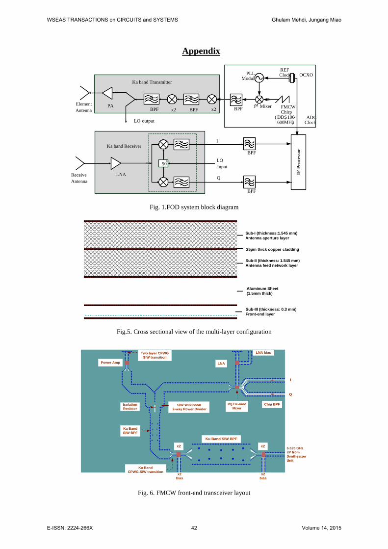
cost, high performance and high-density integration of front-end components on a single substrate layer and its subsequent integration with antenna subsystem. The two layer FOD slot array antenna is described in section IV. The front-end transceiver is to be stacked over the antenna layer. Fig. 5 illustrates the cross-sectional view of the layers employed in the design of integrated FOD sensor. The TWSA antenna aperture is realized on Sub-I layer (thickness: 1.545 mm) while Sub-II layer (thickness: 1.545 mm) is utilized for antenna feed network. The signal transition between the two layers is accomplished by means of aperture slot coupling realized on 50 µm thick copper layer between Sub-I and Sub-II layers. The front-end layer is stacked on the bottom of transmit and receive antennas. Transmit and receive antennas are identical and each occupies 6.8cm*5.3cm area. The two antennas are placed 1cm apart. Thus, the total space available for front-layer is 6.8cm*11.3cm. A 1.5 mm thick metallic sheet in inserted between the antenna feed network and front-end layers. The sheet allows installing the coaxial bead for inter-connection between the two layers. Secondly, the sheet also acts as heat sink to remove the heat generated by the front-end active components. Additionally, the metallic layer provides mechanical strength to the whole integrated module.
The functional blocks of the front-end were discussed earlier in section III and the block diagram is illustrated in Fig. 1. The front-end comprises of passive structures like BPFs, power dividers etc all realized on SIW. The interconnection between MMICs and passive components is accomplished by means of CPWG lines. Front-end design is realized on 12 mil thick R4003C. Since the substrate thickness of antenna feed network is five times larger than the thickness of the front-end substrate, waveguide impedance of the two layers is significantly different. Therefore, the performance of aperture coupling between the two layers with different thickness is poor. In order to accomplish such transition, a coaxial bead transition is employed. The layout of Ka-band FMCW front-end transceiver is depicted in Fig. 6. Transmit and receive ports of the front-end are connected to corresponding antennas ports by means of CPWG-to-SIW transition using coaxial beads. The other end of the 50 ohm CPWG line is connected with the LNA. Afterwards, an I/Q de-modulator is used for down conversion. The Tx block comprises of frequency multiplier and power amplifier MMICs and SIW passive structures.
WSEAS TRANSACTIONS on CIRCUITS and SYSTEMS Ghulam Mehdi, Jungang Miao
E-ISSN: 2224-266X 37 Volume 14, 2015

Detailed design of each component is given the subsequent sections.
5.1 Transmitter Block The block diagram of the Tx block of the front-end is depicted in Fig. 7. In order to generate spurious free and low phase noise Ka-band LFM signal, frequency multipliers and SIW band-pass filters are employed in a cascaded fashion. An optimum circuit configuration in terms of space, cost and performance is adopted to transform 6.625 GHz to 26.5 GHz signal. SIW technology is opted for realization of harmonic suppression BPFs in the Tx block. Besides the advantages of fabrication ease and integration with planar circuits, SIW filters exhibits high Q and low-loss performance. Further, the filters realized in SIW technology are immune to EM interface. 5.1.1 Ku-band SIW BPF SIW filters are attractive replacement of conventional rectangular waveguide filters offering similar performance. A 4-pole Chebyshev Ku-band SIW BPF is realized for harmonic suppression in the Tx block. The filter adopts dual inductive post type configuration and designed in Ansoft HFSS [26]. The primary advantage of dual inductive post configuration is that the diameter of all the posts in the design can be set equal and arbitrarily. This provision allows ease of manufacturability. Since a relatively large diameter value can be selected, consequently, the filter becomes less sensitive to the manufacturing tolerances. Secondly, since no second order mode is excited, it is expected that the higher-order fields would be smaller in this case for given susceptance [27]. Additionally, a CPWG-to-SIW transition similar to the section IV is designed at Ku-band to integrate the filter with planar CPWG line. In the design, the SIW via diameter and pitch is set to 0.5mm and 0.9mm respectively. The SIW channel width is then determined using expression (1). The symmetric dual inductive post in a waveguide exhibits reactance characteristics, and thus can be considered as an inverter [28]. The cavity between the posts behaves as a half-wavelength. The cross-sectional view of dual symmetric posts along with its equivalent circuit and equivalent K-inverter model are illustrated in Fig. 8 (top) and (bottom) respectively.
Once the physical lengths are known, and then the diameter of the posts and their separation distance is optimized for improved insertion and return loss. The layout of the BPF is illustrated in Fig. 9 and the dimensions of the filter are given in Table 3. The
HFSS simulation results in Fig. 10 show that the insertion loss, return loss and bandwidth of the filter are 1 dB, 20dB and 1.9 GHz respectively.
a
b
c c
jX
jXK
Ф/2 Ф/2
Fig. 8. (top) Cross-sectional view and equivalent model of dual symmetric post (bottom) Equivalent K
8 10 12 14 16-60
-40
-20
0
mag
nitu
de (d
B)
Frequency (GHz)
dB S(1,1) dB S(2,2) dB S(2,1)
Fig.10. Ku-band SIW BPF simulated response
5.1.2 Ka-band SIW BPF The harmonic suppression filter at Ka-band adopts the same configuration and design procedure as described in 5.1.1. The 3-pole BPF along with SIW-to-CPWG transition is designed at 26.5 GHz center frequency. The layout of the BPF is illustrated in Fig. 11 and the dimensions of the filter are given in Table 3. The HFSS simulation results are given in Fig. 12. The frequency multipliers in the Tx chain produce two strong harmonics signals at 19.875 GHz and 33.125 GHz. The designed BPF exhibits suppression of 45 dB and 16 at these two corresponding frequencies. The insertion loss of the filter with the SIW-to-CPWG transition is 1.2 dB and return loss is better than 15 dB. The filter is centered at 27 GHz and with 4 GHz 3dB bandwidth.
WSEAS TRANSACTIONS on CIRCUITS and SYSTEMS Ghulam Mehdi, Jungang Miao
E-ISSN: 2224-266X 38 Volume 14, 2015

20 24 28 32-60
-40
-20
0
mag
nitu
de (d
B)
Frequency (GHz)
dB S(1,1) dB S(2,2) dB S(2,1)
Fig. 12. Ka-band SIW BPF simulated response
5.1.3 Ka-band SIW power divider In zero-IF FMCW systems, the same signal being transmitted is injected to the down conversion mixer for generation of beat frequency signal. A directional coupler or a two-way power divider is employed for this function. Power combiners/dividers are one of the key passive components in microwave and mmW systems. In the design of power dividers, it often desirable to obtain high isolation, low loss and low reflection at all the ports. In order to attain a high isolation, Wilkinson type SIW power divider is opted in this work [30]. Wilkinson configuration type power dividers exhibits improved isolation than the conventional T-junction and Y junction lossless power dividers. The power divider discussed in section IV is low loss and show low input return loss, however, being a reciprocal network it cannot be matched at all ports simultaneously. Thus, the divider shows relatively poor isolation and out put return loss. The equivalent circuit of Wilkinson type power divider is illustrated in Fig. 13. The divider comprises of two quarter-wave length line segment and an isolation resistor joins these two line segments. In the design, the Wilkinson equivalent circuit is realized by two half mode SIW (HMSIW) sections connected via an isolation resistor.
The power divider is realized on R4003 (Er: 3.55, thickness= 12 mils, tanσ: 0.0027) for frequency range from 26-27 GHz. The SIW channel width (a) is kept same as that of antenna feed network power divider channel. The characteristic impedance (Z0) of the SIW channel is characterised at the center frequency. The resistance (R) of the isolation resistor is selected such as it is twice of Z0 (R = 2 Z0). A 42 ohm TFR resistor is used to bridge the two
quarter wavelength line segments. The HMSIW width (W1) is about one half of the SIW channel width (a). The slot width (W2) between the HMSIW is about λg /16. During the design of the power divider, the parametric analysis indicates the dependency of isolation between the out ports is highly dependent on the slot length segments L1 and L2. The slot length segment L1 is slightly shorter than the quarter wavelength whereas the slot length segment L2 is optimized for improved isolation. Further the gap (L3) between the isolation resistor and the middle via fence is optimized for improved output return loss in the Y-type junction section of the power divider. The divider added with microstrip transitions is designed in ADS Momentum®. The layout of the power divider is shown in Fig. 14 and the optimized parameters are listed in Table 4. The simulation response of the power divider is illustrated in Fig. 15. The divider exhibits 3 GHz impedance bandwidth for -10 dB return loss at input and output ports. Further, the insertion loss and isolation is 3.8 and 18 dB at 27 GHz. 5.2. Antenna-transceiver transition design The front-end layout is realized on 12 mils thick R4003C whereas the feed network layer of substrate integrated antenna is realized on 60mils thick R4003C. Due to the different wave impedances of the two layers, a series aperture coupled transition could not be employed in this particular scenario. In order to interface the two SIW channels realized on 12 mil and 60 mil thickness respectively, our proposed solution adopts a RF coaxial bead. The transition comprises of a right-angled junction of waveguide and coaxial line, where the center conductor pin of the coaxial line extends through the broad wall into 60 mil SIW and acts as a coupling probe inside. The probe in the SIW acts as an impedance transformer from the low impedance of the coaxial line, typically 50 Ω, to the high impedance of the SIW which is about 80 Ω in this case. The match is accomplished by adjusting the back-short distance and the length of the center conductor probe. The probe is placed at the center to intercept maximum electric field. The equivalent model of the transition is shown in Fig. 16. The resistor on the right side of the model represents the SIW and is equal to the SIW impedance. The transition is represented by a capacitive reactance, in series with the coaxial line. SIW is shunted with the equivalent susceptance of the SIW stub, the left part of the waveguide [31].
WSEAS TRANSACTIONS on CIRCUITS and SYSTEMS Ghulam Mehdi, Jungang Miao
E-ISSN: 2224-266X 39 Volume 14, 2015

Fig. 17 illustrate the cross sectional view of the two layer transition. The height of the coaxial bead is 1.5 mm. A 1.5 mm thick metallic sheet in inserted between the two substrate layers to install the coaxial bead. The metallic sheet also acts as heat sink to remove the heat generated by the front-end active components. The metallic layer further provides mechanical strength the whole interrogated module. The impedance match between the two layers is accomplished by adjusting the back-short distance l and the length of the center conductor probe d inside the 60 mils thick substrate. Since the maximum electric field is at the center of the wide dimension of the waveguide, the probe is placed in the center. The initial values of d and l are computed from expressions given in [32] and later the transition is simulated and optimized in HFSS. The optimum back-short distance l is 1.717 mm and pin length d is 1.228 mm. The geometric dimensions of the transition are given in Table 5. The simulated response of the transition is given in Fig. 18.
22 24 26 28 30-20
-15
-10
-5
0
mag
nitu
de (d
B)
Frequency (GHz)
dB S(1,1) dB S(2,2) dB S(2,1)
Fig. 18. Two layer transition Simulated response 5 Conclusion A capability demonstration model for a Ka-band FOD detection sensor employing multi-layer system-on-substrate approach is presented. New concepts are introduced for realization of low-cost, high performance and ultra-compact FOD sensors. The previously reported mmW SoS systems and sub-systems are realized on single-layer substrate occupying relatively larger space. Firstly, the concept of multi-layer system-on-substrate is introduced in this work. Secondly, the design of a planar travelling-wave type slot array antenna in SIW technology is presented. A virtually grounded resistive matched load is introduced. Moreover, in order to couple two SIW substrate layers with
different thicknesses, a coaxial bead is introduced for low-loss coupling between the two channels. Substrate integrated circuits are employed for design of all the passive structures in the design. The proposed design methodology can be adopted for development of other low-cost commercial mmW products. References: [1] A. Circular, “150/5210-24: Airport Foreign
Object Debris (FOD) Management.” FAA, Washington, DC, 2010.
[2] B. Razavi, “Design considerations for direct-conversion receivers,” Circuits Syst. II Analog Digit. Signal Process. IEEE Trans., vol. 44, no. 6, pp. 428–435, 1997.
[3] G. Mehdi and J. Miao, “Millimeter wave FMCW radar for Foreign object debris (FOD) detection at airport runways,” in Applied Sciences and Technology (IBCAST), 2012 9th International Bhurban Conference on, 2012, pp. 407–412.
[4] N. Yonemoto, A. Kohmura, S. Futatsumori, T. Uebo, and A. Saillard, “Broad band RF module of millimeter wave radar network for airport FOD detection system,” in Radar Conference-Surveillance for a Safer World, 2009. RADAR. International, 2009, pp. 1–4.
[5] P. Feil, W. Menzel, T. P. Nguyen, C. Pichot, and C. Migliaccio, “Foreign objects debris detection (FOD) on airport runways using a broadband 78 GHz sensor,” in Microwave Conference, 2008. EuMC 2008. 38th European, 2008, pp. 1608–1611.
[6] L. Yan, W. Hong, K. Wu, and T. J. Cui, “Investigations on the propagation characteristics of the substrate integrated waveguide based on the method of lines,” in Microwaves, Antennas and Propagation, IEE Proceedings, 2005, vol. 152, no. 1, pp. 35–42.
[7] Z. Li and K. Wu, “24-GHz frequency-modulation continuous-wave radar front-end system-on-substrate,” Microw. Theory Tech. IEEE Trans., vol. 56, no. 2, pp. 278–285, 2008.
[8] F. F. He, K. Wu, W. Hong, L. Han, and X.-P. Chen, “Low-cost 60-GHz smart antenna receiver subsystem based on substrate integrated waveguide technology,” Microw. Theory Tech. IEEE Trans., vol. 60, no. 4, pp. 1156–1165, 2012.
[9] S. V. Hum, M. Okoniewski, and R. J. Davies, “Modeling and design of electronically tunable reflectarrays,” Antennas Propagation, IEEE Trans., vol. 55, no. 8, pp. 2200–2210, 2007.
WSEAS TRANSACTIONS on CIRCUITS and SYSTEMS Ghulam Mehdi, Jungang Miao
E-ISSN: 2224-266X 40 Volume 14, 2015

[10] M. I. Skolnik, “Introduction to radar systems,” 2001.
[11] J. Lee, Y.-A. Li, M.-H. Hung, and S.-J. Huang, “A fully-integrated 77-GHz FMCW radar transceiver in 65-nm CMOS technology,” Solid-State Circuits, IEEE J., vol. 45, no. 12, pp. 2746–2756, 2010.
[12] N. J. Willis and H. Griffiths, Advances in bistatic radar. SciTech Publishing, 2007.
[13] A. K. Gorwara and D. Parker, “DESIGN AND PERFORMANCE OF A FREQUENCY DIVIDE-MULTIPLY CASCADE FOR TRANSPONDER APPLICATIONS,” in International Conference on Communications, 11 th, San Francisco, Calif, 1975, pp. 14–36.
[14] F. Jin, G. Wan, Q. Wang, and J. Zhang, “A Simulation Model of the Positioning Accuracy in the Multi-radar Foreign Object Debris Detection System,” in in Unifying Electrical Engineering and Electronics Engineering, Springer, 2014, pp. 1407–1414.
[15] P. Feil, A. Zeitler, T. P. Nguyen, C. Pichot, C. Migliaccio, and W. Menzel, “Foreign object debris detection using a 78 GHz sensor with cosec antenna,” in Radar Conference (EuRAD), 2010 European, 2010, pp. 33–36.
[16] M. Ferri, G. Giunta, A. Banelli, and D. Neri, “Millimetre wave radar applications to airport surface movement control and foreign object detection,” in Radar Conference, 2009. EuRAD 2009. European, 2009, pp. 437–440.
[17] D. Deslandes and K. Wu, “Single-substrate integration technique of planar circuits and waveguide filters,” Microw. Theory Tech. IEEE Trans., vol. 51, no. 2, pp. 593–596, 2003.
[18] S. R. Rengarajan, “Theory of a traveling wave feed for a planar slot array antenna,” in General Assembly and Scientific Symposium, 2011 XXXth URSI, 2011, pp. 1–4.
[19] R. A. Gilbert, “Waveguide Slot Antenna Arrays,” Antenna Eng. Handbook., 2007.
[20] K. E. Rodrigo and M. B. Perotoni, “Slotted waveguide antenna design using 3D EM simulation,” Microw. J., pp. 1–5.
[21] D. Deslandes, “Design equations for tapered microstrip-to-substrate integrated waveguide transitions,” in Microwave Symposium Digest (MTT), 2010 IEEE MTT-S International, 2010, pp. 704–707.
[22] D. M. Pozar, Microwave engineering. Wiley. com, 2009.
[23] R. Kazemi, R. A. Sadeghzadeh, and A. E. Fathy, “Design of a wide band eight-way compact SIW power combiner FED by a low loss GCPW-to-SIW transition,” Prog.
Electromagn. Res. C, vol. 26, pp. 97–110, 2012.
[24] S. Germain, D. Deslandes, and K. Wu, “Development of substrate integrated waveguide power dividers,” in Electrical and Computer Engineering, 2003. IEEE CCECE 2003. Canadian Conference on, 2003, vol. 3, pp. 1921–1924.
[25] A. Suntives and R. Abhari, “Transition structures for 3-D integration of substrate integrated waveguide interconnects,” Microw. Wirel. Components Lett. IEEE, vol. 17, no. 10, pp. 697–699, 2007.
[26] H. Gruenberg, “Symmetrically Placed Inductive Posts in Rectangular Wave Guide,” Can. J. Phys., vol. 30, no. 3, pp. 211–217, 1952.
[27] A. Adabi and M. Tayarani, “Substrate integration of dual inductive post waveguide filter,” Prog. Electromagn. Res. B, vol. 7, pp. 321–329, 2008.
[28] N. Marcuvitz, Waveguide handbook, vol. 21. Iet, 1951.
[29] G. L. Matthaei, L. Young, and E. M. T. Jones, Microwave filters, impedance-matching networks, and coupling structures, vol. 5. McGraw-Hill New York, 1964.
[30] K. Kim, J. Byun, and H.-Y. Lee, “Substrate integraged waveguide Wilkinson power divider with improved isolation performance,” Prog. Electromagn. Res. Lett., vol. 19, pp. 41–48, 2010.
[31] R. B. Keam and A. G. Williamson, “Broadband design of coaxial line/rectangular waveguide probe transition,” in Microwaves, Antennas and Propagation, IEE Proceedings, 1994, vol. 141, no. 1, pp. 53–58.
[32] P. Delmotte, “Waveguide-coaxial line transitions,” Belgian Microw. Roundtable, 2001.
WSEAS TRANSACTIONS on CIRCUITS and SYSTEMS Ghulam Mehdi, Jungang Miao
E-ISSN: 2224-266X 41 Volume 14, 2015
Appendix
Ka band Receiver
90° LOInput
I
QReceiveAntenna
Ka band Transmitter
LO output
ElementAntenna
IF P
roce
ssor
ADC Clock
BPF
OCXO
1st Mixer
REFClock
FMCW Chirp
( DDS, 100-600MHz)
z
PLLModule
BPF
BPFBPF BPFx2 x2PA
LNA
Fig. 1.FOD system block diagram
Sub-I (thickness:1.545 mm)Antenna aperture layer
Sub-II (thickness: 1.545 mm)Antenna feed network layer
Aluminum Sheet (1.5mm thick)
Sub-III (thickness: 0.3 mm)Front-end layer
25µm thick copper cladding
Fig.5. Cross sectional view of the multi-layer configuration
Ku Band SIW BPF
Ka Band SIW BPF
SIW Wilkinson 2-way Power Divider
x2x2
I/Q De-mod Mixer
6.625 GHz I/P from Synthesizer Unit
Chip BPF
Q
Ka Band CPWG-SIW transition x2
biasx2
bias
I
LNA bias
LNAPower Amp
Two layer CPWG SIW transition
Isolation Resistor
Fig. 6. FMCW front-end transceiver layout
WSEAS TRANSACTIONS on CIRCUITS and SYSTEMS Ghulam Mehdi, Jungang Miao
E-ISSN: 2224-266X 42 Volume 14, 2015

CLK to DSP
Ka band Transmitter
LO output
ElementAntenna
Synthesizer Unit
BPF BPFx2 x2PA
6.625 GHz
Fig. 7. Block diagram of Tx block
1G3G 5G
2G4G
1L 2L
1D
2D
6G
3L
3D
7G1W
2W
Fig. 9. Ku-band SIW harmonic suppression BPF layout
1G 3G 5G
2G4G
1L 2L
1D
2D6G
3L
3D
8G
7G1W
2W
Fig. 1. Ka-band (26.5GHz) SIW harmonic suppression BPF layout
Port1
Port3
Port2
R02Z
02Z
0.25 gλ
0.25 gλ0Z
0Z
0Z
Fig. 2. Wilkinson type power divider equivalent circuit
WSEAS TRANSACTIONS on CIRCUITS and SYSTEMS Ghulam Mehdi, Jungang Miao
E-ISSN: 2224-266X 43 Volume 14, 2015

Port1
Port3
Port2
a=5.1mm
1.85mm
2mm
HMSIW region
W1
L1
L2L3
Isolation resistor
W20.69mm
Fig. 3.Ka-band SIW two-way Wilkinson power divider layout
25 26 27 28 29-25
-20
-15
-10
-5
0
RL (d
B)
Freq (GHz)
dB S(1,1) dB S(2,2) dB S(3,3)
25 26 27 28 29-2
-3
-4
-5
S21
(dB)
Freq (GHz)
dB S(2,1) dB S(3,1)
(a) (b)
25 26 27 28 29-200
-100
0
100
200
phas
e (d
eg)
Freq (GHz)
S (2,1) S (3,1)
25 26 27 28 29-20
-15
-10
Isol
atio
n (d
B)
Freq (GHz)
dB S(3,2)
(c) (d)
Fig. 4. Two-way SIW Wilkinson PD simulation results (a) RL (b) S21 (c) phase (d) isolation
WSEAS TRANSACTIONS on CIRCUITS and SYSTEMS Ghulam Mehdi, Jungang Miao
E-ISSN: 2224-266X 44 Volume 14, 2015

waveguide50 ohm coaxial-line
Fig. 16. Waveguide-to-microstrip transition equivalent model
12 mil substrate Copper cladding
1.5mm metal sheet60 mil substrate Teflon bead
D1
d
LP
Fig. 5.Cross-sectional view of the two layer transition
Table 3. Dimensions of Ku and Ka band SIW BPFs for harmonic suppression
Filter
Type
Parameters & Dimensions (mm)
G1 G2 G3 G4 G5 G6 G7 D1 D2 D3 L1 L2 L3 W1 W2
Ku-band 2.29 6.8 3.19 5.0 0.9 1.15 0.13 0.5 1 0.25 5.6 6.5 3.25 0.46 3.5
Ka-band 1.02 3.07 1.32 2.37 0.9 0.65 0.13 0.5 0.4 0.25 2.95 3.29 1.55 0.46 1.9
Table 4. Optimized dimensions of 2-way SIW Wilkinson power divider
Parameter L1 L2 L3 W1 W2
Dimension (mm) 2.68 1.32 1.56 2.4 0.49
Table 5. Optimized dimensions of two layer transition
Parameter Dimenssion(mm)
Glass epoxy diameter (D1) 1.85 Pin diameter (d) 0.3 Pin hight in the waveguide (LP) 1.228 Back-short duistance (l) 1.717
WSEAS TRANSACTIONS on CIRCUITS and SYSTEMS Ghulam Mehdi, Jungang Miao
E-ISSN: 2224-266X 45 Volume 14, 2015