a two-layer substrate integrated waveguide out-of … two-layer substrate integrated waveguide...
TRANSCRIPT
A Two-Layer Substrate Integrated Waveguide
Out-of-Phase Power Divider
Qi Chen and Jun Xu School of Physical Electronics, University of Electronic Science and Technology of China, Chengdu, China
Email: [email protected], [email protected]
Abstract—Substrate integrated waveguides (SIWs) have
been proposed and applied to develop a two-way out-of-
phase power divider in this paper. This newly proposed
structure shows good performance in wide frequency range
from 8.6 GHz to 10.6 GHz. The proposed multilayer SIW
out-of phase power divider consists of two layer of
substrates of Rogers 5880 with thickness of 0.508
millimeters. The input at the upper layer is coupled to two
outputs at the lower layer by a narrow metal slot located in
the broad wall of waveguide. The proposed power divider
shows low insertion loss in a wide passband and good
outputs imbalance. In the frequency range from 8.6 GHz to
10.6 GHz, the insertion losses are between -3.32 dB and -
3.66 dB, with return losses less than -10 dB. At the same
time, the magnitude differences between two outputs S21
and S31 are within 0.27 dB. The phase differences between
two outputs are as low as 180 0.8 .The advantage of this
structure is its good performance in wide frequency range
from 8.6 GHz to 10.6 GHz. Also, the proposed structure has
low profile and is easy and cheap to fabricate. The SIW
structure can be integrated easily with other planar circuits
such as microstrip circuits .
Index Terms—power divider, substrate integrated
waveguide, multilayer
I. INTRODUCTION
Traditional waveguide has advantages of low insertion
loss and high-power handling capacities, but its large size
and high cost limit its applies especially in cases that
allow only small volume and light weight. Recently a
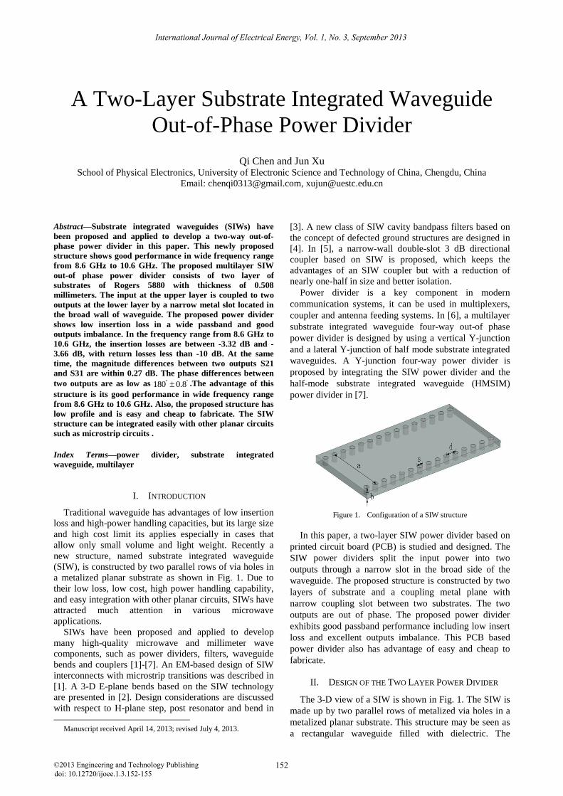
new structure, named substrate integrated waveguide
(SIW), is constructed by two parallel rows of via holes in
a metalized planar substrate as shown in Fig. 1. Due to
their low loss, low cost, high power handling capability,
and easy integration with other planar circuits, SIWs have
attracted much attention in various microwave
applications.
SIWs have been proposed and applied to develop
many high-quality microwave and millimeter wave
components, such as power dividers, filters, waveguide
bends and couplers [1]-[7]. An EM-based design of SIW
interconnects with microstrip transitions was described in
[1]. A 3-D E-plane bends based on the SIW technology
are presented in [2]. Design considerations are discussed
with respect to H-plane step, post resonator and bend in
Manuscript received April 14, 2013; revised July 4, 2013.
[3]. A new class of SIW cavity bandpass filters based on
the concept of defected ground structures are designed in
[4]. In [5], a narrow-wall double-slot 3 dB directional
coupler based on SIW is proposed, which keeps the
advantages of an SIW coupler but with a reduction of
nearly one-half in size and better isolation.
Power divider is a key component in modern
communication systems, it can be used in multiplexers,
coupler and antenna feeding systems. In [6], a multilayer
substrate integrated waveguide four-way out-of phase
power divider is designed by using a vertical Y-junction
and a lateral Y-junction of half mode substrate integrated
waveguides. A Y-junction four-way power divider is
proposed by integrating the SIW power divider and the
half-mode substrate integrated waveguide (HMSIM)
power divider in [7].
Figure 1. Configuration of a SIW structure
In this paper, a two-layer SIW power divider based on
printed circuit board (PCB) is studied and designed. The
SIW power dividers split the input power into two
outputs through a narrow slot in the broad side of the
waveguide. The proposed structure is constructed by two
layers of substrate and a coupling metal plane with
narrow coupling slot between two substrates. The two
outputs are out of phase. The proposed power divider
exhibits good passband performance including low insert
loss and excellent outputs imbalance. This PCB based
power divider also has advantage of easy and cheap to
fabricate.
II. DESIGN OF THE TWO LAYER POWER DIVIDER
The 3-D view of a SIW is shown in Fig. 1. The SIW is
made up by two parallel rows of metalized via holes in a
metalized planar substrate. This structure may be seen as
a rectangular waveguide filled with dielectric. The
152©2013 Engineering and Technology Publishingdoi: 10.12720/ijoee.1.3.152-155
International Journal of Electrical Energy, Vol. 1, No. 3, September 2013

diameter of via holes is s and the thickness of substrate is
b. The distance between two rows of via holes is a, and
the distance between two adjacent via holes in same row
is d. It is obvious that the SIW is period structure with
period length of d.
Since the SIW is a quasi-rectangular waveguide, the
cutoff frequencies of the SIW modes cmnf can be
calculated as follow [1], [8]:
2 21( ) ( )
2Cmn
eqv
m nf
a b
(1)
where eqva and b are equivalent width and height of
SIW, m and n represent mode order numbers, and
are permeability and permittivity, respectively. The cutoff
frequency for dominant mode 10TE can be calculated as,
10
1
2C
eqv
fa
(2)
For the structure shown in Fig. 1, We can calculate the
equivalent width eqva as follow
2 2
eqv 1.08 0.1d d
a as a
(3)
Two useful empirical criteria to establish upper bounds
for s and d are
2s d (4)
5
gd
(5)
where g is the guided wavelength. For the dominant
mode 10TE ,
102
2 2
2
2
( ) ( )
g
r
c a
(6)
If the first higher-order mode propagating along the
SIW is the 0TEm mode, from (2) and (4) an upper limit
for the via diameter is given by
2
2
5 1
ad
m
(7)
Figure 2. The structure of the proposed SIW power divider
Fig. 2 shows the structure of the proposed two-layer
out-of-phase SIW based power divider with narrow
coupling slots.
As shown in Fig. 2, the power divider is built on two
0.508 mm-thick substrates of Rogers 5880 with relative
permittivity of 2.2 and loss tangent of 0.0009. The
coupling metal plane with a narrow coupling slot locates
between two substrates. The mode power of the input
SIW in the upper substrate is coupled through the narrow
slot in the coupling metal layer and divided into two out-
of-phase outputs in a lower substrate.
As the SIW structure could not be connect to a
network analyzer directly, a microstrip-to-SIW transitions
are designed to connected SIW and the 50-ohm
microstrip to make the measurements. The designed
microstrip-to-SIW transitions is shown in Fig. 3. A
triangle tapered line is employed in the designed
microstrip-to-SIW transition. Good performance could be
achieved by optimization of the angle and length of the
triangle tapered line.
Figure 3. The proposed microstrip-to-SIW transition
The design of the proposed power divider with
microstrip-to-SIW transitions is shown in Fig. 4. The
width of the 50-ohm microstrip is W1. The length and
width of the triangle tapered line in the microstrip-to-SIW
transition section are L1 and W2. The length and width of
the input SIW in the upper substrate and output SIW in
the lower substrate are L2 , W3 and L6, W6, respectively.
The length and width of the coupling slot locates at the
metal plane between two substrates are L3 and W4.
Figure 4. Design of the proposed power divider with microstrip-to-SIW transitions
The width of SIW(W3, W6) is designed for working in
the frequency of X-band. The dimensions of via holes (s
and d), which are designed to reduce leakage from the
substrate integrated waveguide structure, can be decided
by formulas (4) and (5).
153©2013 Engineering and Technology Publishing
International Journal of Electrical Energy, Vol. 1, No. 3, September 2013

TABLE I. PARAMETERS OF THE PROPOSED POWER DIVIDER
(UNIT: MILIMETERS)
Dimensions values Dimensions values
W1 1.58 L2 18.11
W2 8.96 L3 7.94
W3 19.01 L4 4.11
W4 0.052 L5 13.05
W5 8.96 L6 68
W6 19.01 s 2
L1 13.05 d 1
Table I gives the dimensions of the proposed two-way
out-phase power divider. The thickness of the coupling
metal plane between two substrates is 0.034 millimetres.
III. RESULTS
The top view of the proposed SIW power divider with
microstrip-to-SIW transitions is shown in Fig. 5. The
input port (port1 in Fig. 5) locates at the upper substrate
while the two outputs (port2 and port3) locate at the
lower layer substrate. The proposed structure was built
with a two-layer substrate with thickness of 0.508 mm,
relative dielectric constant of 2.2 and loss tangent of
0.0009. The impedance of input and output microstrip
was designed to 50 ohms at a center frequency of 9.5
GHz.
Three microstrip-to-SIW transitions in the proposed
structure were designed to connect the microstrip lines
and the SIWs. The input power come in from a 50-ohm
microstrip and then come through a microstrip-to-SIW
transition before arriving at the SIW structure. A narrow
slot was employed to divide the input power into two way
outputs. The two outputs with 180 degrees phase
difference go through the output SIW in the opposite
direction. In order to facilitate measurements, microstrip-
to-SIW transitions are used to transform the SIW to 50-
ohm microstip.
Port2 Port1 Port3
Figure 5. Top view of the proposed SIW power divider with microstrip-to-SIW transitions
The simulations are carried out using Ansoft HFSS
package. Fig. 6 shows the optimized results of the SIW
power divider As shown in Fig. 6, in a wide frequency
range from 8.6 GHz to 10.6 GHz, the return losses are
less than -10 dB, and the insertion losses are between -
3.32 dB and -3.66 dB. The magnitude differences
between two outputs S21 and S31 are within 0.27 dB in
the frequency range from 8.6 to 10.6 GHz.
8 9 10 11
-15
-10
-5
0
S p
ara
me
ters
(d
B)
Frequency (GHz)
S11
S21
S31
Figure 6. The optimized result of the SIW power divider
Fig. 7 shows the phase differences between 21S and
31S . We can see from the figure that the phase
differences between two output are relatively low. Over a
wide frequency range from 8 to11 GHz, the phase
differences between two outputs are as low as180 0.8 .
8 9 10 11
179.0
179.5
180.0
180.5
181.0
Ph
ase
va
ria
tio
n (
de
gre
e)
Frequency (GHz)
Figure 7. Phase difference between the output ports
IV. CONCLUSION
This paper presents and demonstrates a two-way out-
phase power divider based on two-layer substrate-
integrated waveguides. In the proposed structure, an input
SIW in a upper layer is divided into two output SIWs in a
lower layer by coupling the energy from a narrow slot
etched on the broad side of the SIW.
The proposed power divider shows good performance
in a wide range of frequency. Simulated results show that
the out-of-phase power divider exhibits low passband
insertion loss in a broad bandwidth. The outputs
imbalance is also very good. The proposed structure has
advantages of cheap to fabricate, compact in size and
easy to integrate with planar circuits. The proposed out-
of-phase power divider can be served as a building block
in millimeter-wave systems.
154©2013 Engineering and Technology Publishing
International Journal of Electrical Energy, Vol. 1, No. 3, September 2013

REFERENCES
[1] J. E. Rayas-Sanchez and V. Gutierrez-Ayala, "A general EM-based design procedure for single-layer substrate integrated
waveguide interconnects with microstrip transitions,” in Proc. Microwave Symposium Digest, IEEE MTT-S International, 2008,
pp. 983- 986.
[2] B. Y. E. Khatib, T. Djerafi, and K. Wu, "Substrate-integrated waveguide vertical interconnects for 3-D integrated circuits,”
IEEE Trans. Components Packaging And Manufacturing Technology, vol. 2, no. 9, pp. 1526-1535, Sep. 2012.
[3] D. Deslandes and K. Wu, "Design consideration and performance
analysis of substrate integrated waveguide components," in Proc. European Microwave Conference, Milan, Italy, Sep. 2002, pp.
881-884. [4] Y. L. Zhang, W. Hong, K. Wu, J. Xin Chen, and H. J. Tang,
"Novel substrate integrated waveguide cavity filter with defected
ground structure," IEEE Trans. Microw. Theory Tech., vol. 53, no. 4, pp. 1280-1287, Apr. 2005.
[5] B. Liu, W. Hong, Y. Zhang, J. X. Chen, and K. Wu, "Half-mode substrate integrated waveguide (HMSIW) double-slot coupler,"
Electronicis Letters, vol. 43, no. 2, pp. 113-114, Jan. 2007.
[6] D. S. Eom, J. D. Byun, and H. Y. Lee, “Multilayer substrate integrated waveguide four-way out-of-phase power divider,” IEEE
Trans. Microw. Theroy Tech., vol. 57, no. 12, pp. 3469–3476, Dec. 2009.
[7] X. Zou, C. M. Tong, and D. M. Yu, "Y-junction power divider
based on substrate integrated waveguide," Electronics Letter, vol. 47, no. 25, pp.1375-1376, Dec. 2011.
[8] F. Xu and K. Wu, "Guided-wave and leakage characteristics of substrate integrated waveguide," IEEE Trans. Microw. Theory
Tech., vol. 53, no. 1, pp. 66–73, Jan. 2005.
Qi Chen was born in Hunan province, China, in 1984.
He received the B.S. and M.S. degree in radio physics
from University of Electronic Science and Technology of China, Chengdu, China, in 2006 and 2009
respectively. He is currently working towards the Ph.D. degree in radio physics, University of Electronic
Science and Technology of China, Chengdu, China.
His current research interests include advanced microwave and millimeter-wave devices and circuits, substrate integrated waveguide
(SIW) passive components, passive circuits working at frequencies up to 300 GHz.
Jun Xu was born in Chengdu, China, in March 1963. He received the Graduate degree from the Department
of Electromagnetic Engineering, Chengdu Institute of
Radio Engineering, Chengdu, in July 1984. He received the Masters degree in July 1990. In July 2002,
he was granted the Post Ph.D., electronics physics major. Currently, he is Dean of Academic Affairs, School of Physical
Electronics University of Electronic Science and Technology of China.
He joined the University of Electronic Science and Technology of China, Chengdu, in 1984. In June 1998, he was selected as the Project
Person of Ability for the second term at the university. In June 2000, he was promoted to Professor. His current research interests include
electromagnetic theory and microwave technology, millimeter wave
hybrid integrated technology, millimeter wave communication, and radar radio frequency technology.
155©2013 Engineering and Technology Publishing
International Journal of Electrical Energy, Vol. 1, No. 3, September 2013