mrs-fcv3n4 draft.qxd 1/13/2010 12:40 pm page 1mrs.org.sg/outlook/mrs-s outlook vol4...
TRANSCRIPT

To spread information and knowledge and to promote collaboration in the area of Materials Research, Engineeringand Technology amongst the members of MRS-SVol 4 No. 2 October – December 2009 | ISSN 1793-3609
MRS-S Activities: Past, Present and Future
The Materials Research Society of Singapore (MRS-S) organized four International andthree National Conferences in Singapore since 2001. The biennial ‘InternationalConference on Materials for Advanced Technologies (ICMAT)’ series were held in 2001,2003, 2005 2007 and 2009.
The biennial National Conferences were held in 2004, 2006 and 2008. MRS-S also spon-sored/supported several other conferences, workshops, symposia and public lectures.It instituted gold medals for the best outgoing students in Materials Science at theNational University of Singapore (NUS) and Nanyang Technological University (NTU).It instituted the ‘MRS Singapore Student Bursary Fund’ at the National University ofSingapore. MRS-S also instituted the ‘MRS-S Book Prize’ at the ‘Republic Polytechnic’of Singapore. This yearly Book Prize will be awarded to the top final-year student fromthe ‘Diploma in Materials Science’.
To reach out to the public, MRS-S has organized number of public lectures by NobelLaureates and also an Astronaut.
The MRS-S gold medal for the academic year, 2008/2009 at NUS was awarded to Mr.Shi Yezhou of the Faculty of Engineering. Congratulations to him, and MRS-S wishes allthe best in his future academic career.
ICMAT 2009 & IUMRS-ICA 2009 be held during June 28–July 3, 2009 in Singapore.It had 23 Symposia, 9 Plenary and 3 Theme Lectures in addition to the Keynote,Invited, Oral talks and Poster presentations,covering almost all the aspects of materialsscience, engineering and technology. There were 2170 registered participants. Therewas also an Exhibition with 43 Booths, of the products and services by the manufactur-ers, book and journal publishers.
37 Best Poster Awards were given away on the last day of the ICMAT 2009 &IUMRS-ICA 2009 Conference. The List of Symposia, names and addresses of the Award win-ners, and titles of the Posters are listed separately below.
The ICMAT 2011 will be held in Singapore during June, 26-July1, 2011.
C O N T E N T SC O N T E N T SMRS-S MRS-S Activities: Past, PresentActivities: Past, Presentand Future and Future
ppage 26...age 26...HighlightHighlights of previous ICMAs of previous ICMATTConferencesConferences
ppage 27...age 27...HighlightHighlights of previous Nationals of previous NationalConferencesConferences
ppage 27...age 27...List of Symposia List of Symposia
ppage 28...age 28...Materials Education &Materials Education &Research in SingaporeResearch in Singapore
ppage 32...age 32...HighlightHighlights of the Recents of the RecentLiterature Literature
ppage 33...age 33...MRS-S MembershipMRS-S Membership
ppage 34...age 34...Recent BooksRecent Books
ppage 35...age 35...Theme Theme Article Article
ppage 43...age 43...Forthcoming ConferencesForthcoming Conferences
ppage 55...age 55...Theme Theme Articles’Articles’ Appeared inAppeared inVVol. 4 Nos. 1ol. 4 Nos. 1
ppage 56...age 56...InvitInvitation to MRS-S Membersation to MRS-S Members
ppage 57...age 57...
© 2009 MRS-S, Singapore. All rights reserved.
mrs-fcv3n4_draft.qxd 1/13/2010 12:40 PM Page 1
was
MRS-S OUTLOOK Volume 4• No.2• October–December, 2009
MR
S-S
Act
iviti
es:
Pas
t,P
rese
ntan
dF
utur
e
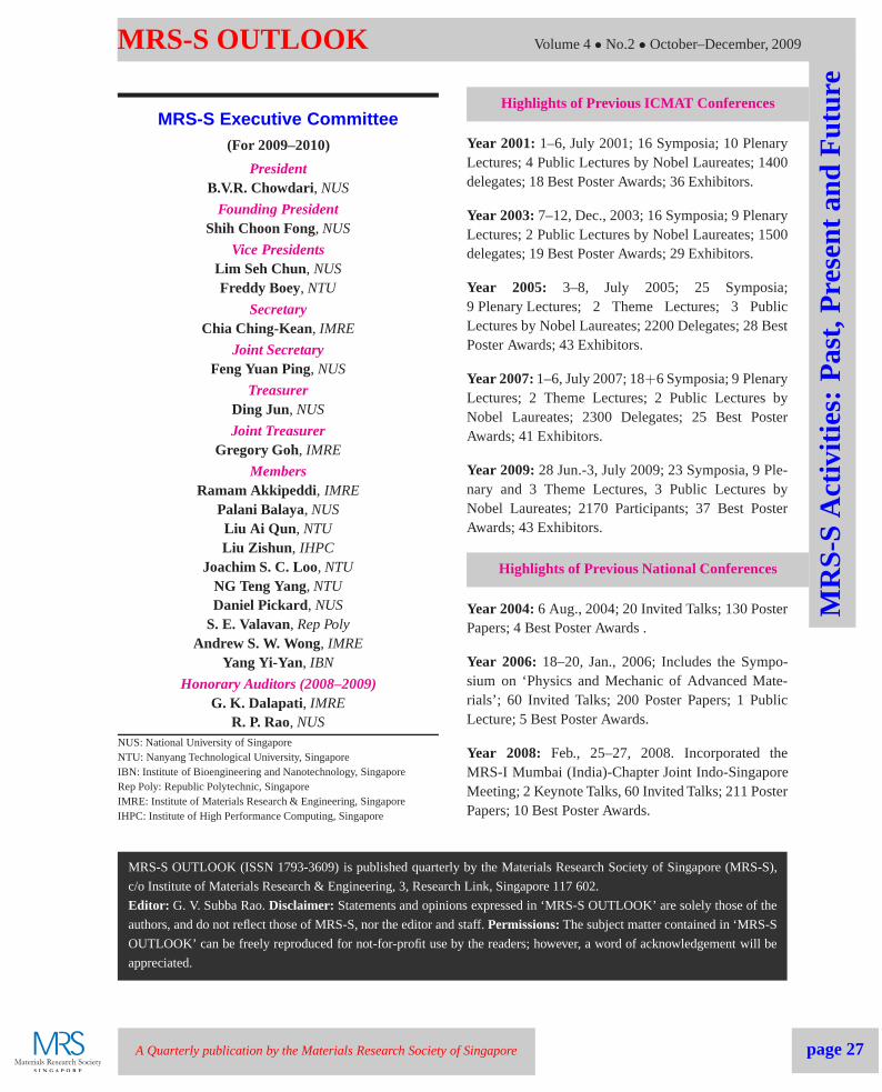
MRS-S Executive Committee(For 2009–2010)
PresidentB.V.R. Chowdari, NUS
Founding PresidentShih Choon Fong, NUS
Vice PresidentsLim Seh Chun, NUSFreddy Boey, NTU
SecretaryChia Ching-Kean, IMRE
Joint SecretaryFeng Yuan Ping, NUS
TreasurerDing Jun, NUS
Joint TreasurerGregory Goh, IMRE
MembersRamam Akkipeddi, IMRE
Palani Balaya, NUSLiu Ai Qun , NTULiu Zishun , IHPC
Joachim S. C. Loo, NTUNG Teng Yang, NTUDaniel Pickard, NUS
S. E. Valavan, Rep PolyAndrew S. W. Wong, IMRE
Yang Yi-Yan, IBN
Honorary Auditors (2008–2009)G. K. Dalapati, IMRE
R. P. Rao, NUSNUS: National University of SingaporeNTU: Nanyang Technological University, SingaporeIBN: Institute of Bioengineering and Nanotechnology, SingaporeRep Poly: Republic Polytechnic, SingaporeIMRE: Institute of Materials Research & Engineering, SingaporeIHPC: Institute of High Performance Computing, Singapore
Highlights of Previous ICMAT Conferences
Year 2001:1–6, July 2001; 16 Symposia; 10 PlenaryLectures; 4 Public Lectures by Nobel Laureates; 1400delegates; 18 Best Poster Awards; 36 Exhibitors.
Year 2003:7–12, Dec., 2003; 16 Symposia; 9 PlenaryLectures; 2 Public Lectures by Nobel Laureates; 1500delegates; 19 Best Poster Awards; 29 Exhibitors.
Year 2005: 3–8, July 2005; 25 Symposia;9 Plenary Lectures; 2 Theme Lectures; 3 PublicLectures by Nobel Laureates; 2200 Delegates; 28 BestPoster Awards; 43 Exhibitors.
Year 2007:1–6, July 2007; 18+6 Symposia; 9 PlenaryLectures; 2 Theme Lectures; 2 Public Lectures byNobel Laureates; 2300 Delegates; 25 Best PosterAwards; 41 Exhibitors.
Year 2009:28 Jun.-3, July 2009; 23 Symposia, 9 Ple-nary and 3 Theme Lectures, 3 Public Lectures byNobel Laureates; 2170 Participants; 37 Best PosterAwards; 43 Exhibitors.
Highlights of Previous National Conferences
Year 2004:6 Aug., 2004; 20 Invited Talks; 130 PosterPapers; 4 Best Poster Awards .
Year 2006: 18–20, Jan., 2006; Includes the Sympo-sium on ‘Physics and Mechanic of Advanced Mate-rials’; 60 Invited Talks; 200 Poster Papers; 1 PublicLecture; 5 Best Poster Awards.
Year 2008: Feb., 25–27, 2008. Incorporated theMRS-I Mumbai (India)-Chapter Joint Indo-SingaporeMeeting; 2 Keynote Talks, 60 Invited Talks; 211 PosterPapers; 10 Best Poster Awards.
MRS-S OUTLOOK (ISSN 1793-3609) is published quarterly by the Materials Research Society of Singapore (MRS-S),
c/o Institute of Materials Research & Engineering, 3, Research Link, Singapore 117 602.
Editor: G. V. Subba Rao.Disclaimer: Statements and opinions expressed in ‘MRS-S OUTLOOK’ are solely those of the
authors, and do not reflect those of MRS-S, nor the editor and staff. Permissions:The subject matter contained in ‘MRS-S
OUTLOOK’ can be freely reproduced for not-for-profit use by the readers; however, a word of acknowledgement will be
appreciated.
A Quarterly publication by the Materials Research Society of Singapore page 27

Volume 4• No.2• October–December, 2009 MRS-S OUTLOOKM
RS
-SA
ctiv
ities
:P
ast,
Pre
sent
and
Fut
ure
ICMAT 2009 & IUMRS-ICA 2009 Conference: List of Symposia & Best Poster Awards
List of Symposia
Symposia A: Advanced Biomaterials and Regenera-tive MedicineSymposia B: Nanomaterials for Bioimaging andBiosensingSymposia C: Advanced Delivery of Therapeutics:New Challenges for MaterialsSymposia D: Functional Ceramic Materials, OxideThin Films and HeterostructuresSymposia E:Nanostructured Magnetic Materials andTheir ApplicationsSymposia F: Nanostructured Materials for Electro-chemical Energy Systems: Lithium Batteries, Superca-pacitors and Fuel CellsSymposia G:Plasmonics and ApplicationsSymposia H: Carbon Nanotubes: Synthesis, Charac-terisation and ApplicationsSymposia I: Carbon Rich Materials (CRMs) andApplicationsSymposia J:Nanodevices and NanofabricationSymposia K: Nano Patterning & Surface Characteri-zation
Symposia L: NEMS/MEMS Technology and DevicesSymposia M: DNA Nanoscience and PhysicsSymposia N:Plastic ElectronicsSymposia O: Compound Semiconductor Photonics:Materials, Devices and IntegrationSymposia P:Optical Fiber Devices and ApplicationsSymposia Q:Computational Materials Design at AllScales: From Theory to ApplicationSymposia R: Single Crystals; Growth and Applica-tions for Research and IndustrySymposia S:Novel Routes of Solution ProcessingSymposia T:Advanced Component Manufacture fromLight MaterialsSymposia U: Mechanical Behavior of Micro- andNano-Scale SystemsSymposia V: Materials Education: New Tools andResourcesSymposia W: GEM4 /SMART Symposium on Infec-tious Diseases
Best Poster Awards
Symp. & PosterCode
Title Authors and Addresses Country
A-S8.008(P) Heparin-immobilized Gold Nanopar-ticles for Targeted Cancer Cell Death.
Kyuri LEE, Hyukjin LEE, Ki HyunBAE, Tae Gwan PARK,Dept. of Biological Sci., KAIST,Daejon, South Korea.
S. Korea
A-S8.047 In Vitro Maturation of Large hfMSC-PCL/TCP Bone Tissue EngineeredConstruct through Long Term Culturein a Biaxial Perfusion Flow Bioreac-tor.
Yuchun LIU, Mark CHONG, Zhiy-ong ZHANG, Woon Shin CHONG,Toon Tien FOO, Yhee Cheng CHNG,Mahesh CHOOLANI, Jerry CHAN,Swee Hin TEOH,Dept. of Mech. Engg., NUS, Singa-pore.
Singapore
A-S8.103 The Use of Carboxymethylcellulose-derived Hydrogel to Control Hepato-cyte Aggregation Behavior and Main-tain Liver-specific Functionin vitro.
Yuko OGUSHI, ShinjiSAKAI, Takayuki TAKEI, HiroyukiIJIMA, Koei KAWAKAMI,Dept. of Chem. Engg., Kyushu Univ.,Fukuoka, Japan
Japan
A Quarterly publication by the Materials Research Society of Singaporepage 28
MRS-S OUTLOOK Volume 4• No.2• October–December, 2009
MR
S-S
Act
iviti
es:
Pas
t,P
rese
ntan
dF
utur
e
B-S8.01 Examination of Au Nanocrystal-Directed Growth ofAu-C2O Core-Shell Nanostructures.
Chun-Hong KUO, Michael H.HUANG,Dept. of Chemistry, National TsingHua University, Hsinchu, Taiwan.
Taiwan
C-S5.19 Shell-detachable Micelles Based onDisulfide-linked Block Copolymeras Potential Carrier for IntracellularDrug Delivery.
Yu-Cai WANG, Ling-Yan TANG,Yang LI, Jin-Zhi DU, Jun WANG,Dept. of Polymer Sci. & Engg.,Univ. of Science and Technol. ofChina, Hefei, China.
China
D-S11.010 Synthesis and Field Emission Proper-ties of Well-Aligned ZnO Nanowireson Buffer Layer.
Wei Li ONG, Cha Yung YU, YingWANG, Chorng Haur SOW, SharonXiaodai LIM, Andrew See WengWONG, Ghim Wei HO,Dept. of Electrical and ComputerEngg., NUS, Singapore.
Singapore
D-S11.040 Relaxation Dynamics in EpitaxialBiFeO3 Thin Films.
Lang CHEN, WeiGang CHEN,School of Mater. Sci. & Engg., NTU,Singapore.
Singapore
D-S11.076 Reducing Gas Response Kinetics ofNanostructured Indium Oxide ThinFilms.
Seetha MAHALINGAM, BharathiSHIVA,Mangalaraj DEVANESAN, NatarajDEVARAJ,Dept. of Physics, Bharathiar Univer-sity, Tamil Nadu, India.
India
D-S11.092 Formation and Characterisation ofCuprous Oxide Film via OxygenPlasma Treatment of Metallic Cop-per.
Chin Chun OOI, Gregory GOH,IMRE, Singapore.
Singapore
E-S5.46 Nanostructured SmCo5 Thin Filmswith Perpendicular Anisotropy.
Lina ZHANG, Jiangfeng HU, Jing-sheng CHEN, Jun DING,Dept. of Mater. Sci. & Engg., NUS,Singapore.
Singapore
E-S5.67 Reduction of Switching Field Distri-bution inBit-patterned Media with Antifer-romagnetically Coupled RecordingLayer.
SuziDENG, S.N. PIRAMANAYAGAM,R. SBIAA, K.O. AUNG,DSI, Singapore.
Singapore
F-S8.05 Isolation of Solid Solution Phases inSize-Controlled LixFePO4 at RoomTemperature.
Genki KOBAYASHI, Shin-IchiNISHIMURA, Min-Sik PARK, RyojiKANNO, Masatomo YASHIMA,Takashi IDA, Atsuo YAMADA,Interdisciplinary Grad. School of Sci.& Engg., Tokyo Inst. of Technol.,Yokohama, Japan.
Japan
F-S8.26 Lithium Ion Conductivity at Inter-faces of Multi-component Systems.
Dominik SAMUELIS, Lijun FU,Xiangxin GUO, Chilin LI, JiyongSHIN, Joachim MAIERMax Planck Institute for Solid StateResearch, Stuttgart, Germany.
Germany
G-S8.02 Surface Enhanced Raman ScatteringObservation on Metal Nanobowls.
Yun MA, Yu Meng YOU, Sureshku-mar CHANDRASEKAR,Chin Leong ONG, Xian Ting ZENG,Ze Xiang SHEN,Division of Phys. & Appl. Phys.,NTU, Singapore.
Singapore
A Quarterly publication by the Materials Research Society of Singapore page 29
Volume 4• No.2• October–December, 2009 MRS-S OUTLOOKM
RS
-SA
ctiv
ities
:P
ast,
Pre
sent
and
Fut
ure
G-S8.14 From Surface EnhancedRaman Spectroscopy (SERS) to TipEnhanced Raman Scattering (TERS):A Raman Enhancement Study UsingIndividual Single-crystalline SilverNanowires.
YuMeng YOU, PURNAWIRMAN,Johnson KASIM, ChaoLing DU,Ting YU, ZeXiang SHEN,Division of Phys. & Appl. Phys.,NTU, Singapore.
Singapore
G-S8.23 Effect of UsingThin Transparent Conductive Layeron Plasmonic Oscillations in MetalNanoparticles Fabricated by ElectronBeam Lithography.
Urcan GULER, Seckin OZTURK,Mustafa KULAKCI, Sedat CANLI,Rasit TURAN,Dept. of Phys., Middle East TechnicalUniversity, Ankara, Turkey.
Turkey
H-S5.15 Comparison between Double- andSingle-Wall Carbon Nanotube EffectTransistors.
Leihua HUANG, Eng Fong CHOR,Yihong WU, Zaibing GUO,Dept. of Electrical and ComputerEngineering, NUS, Singapore.
Singapore
H-S5.18 Simulation of Electron IrradiationEffects in Carbon Nanotubes - Intro-duction of Relativistic Effect.
Masaaki YASUDA, ShinyaWAKUDA, Ryosuke MIMURA,Hiroaki KAWATA, Yoshihiko HIRAI,Dept. of Physics and Electronics,Osaka Prefecture University, Sakai,Japan.
Japan
I-S8.23 Polycyclic Aromatic Hydro-carbons Adsorption on Noble MetalClose Packed Surfaces: An Innova-tive First Step to Fullerenes and Het-erofullerenes.
Giulio BIDDAU, Pablo POU, Gon-zalo OTERO, Jose Angel MAR-TIN GAGO, Taisuke OZAKI, RubenPEREZ,Departamento de Fisica Teorica dela Materia Condensada, UniversidadAutonoma de Madrid, Madrid, Spain.
Spain
I-S8.33 Synthesis of Centimeter-scaledFew-layer Graphene using ChemicalVapor Deposition Method.
Sung-Yen WEI, Zhen-Yu JUANG,Chih-Yu WU, Ang-You LU, Keh-Chyang LEOU, Fu-Rong CHEN,Chuen-Horng TSAI,Dept. of Engg. & System Sci-ence, National Tsing Hua University,Hsinchu, Taiwan.
Taiwan
J-S11.12 Exploiting Self-heating Effect inNanowires.
Roman JIMENEZ-DIAZ, DanielPRADES, Francisco HERNANDEZ-RAMIREZ, Albert CIRERA, AlbertROMANO-RODRIGUEZ, AlbertCORNET, Joan Ramon MORANTE,S BARTH, S MATHUR,Dep. Electronica, UniversitatBarcelona, Barcelona, Spain.
Spain
J-S11.51 Comparative Study of Doping Effecton Reverse-bias-modulated BipolarResistance Switching in Transition-metal Doped ZnO.
Haiyang PENG, Gongping LI,Zhipeng WEI, Tom WU,Division of Phys. & Appl. Phys.,NTU, Singapore.
Singapore
K-S11.08 Non-close-packed Non-spherical Colloidal Particle StructuresFabricated by Combining Pre-heatingand Reactive Ion Etching.
Chunxiao CONG, William ChandraJUNU, Ting YU, Zexiang SHEN,Division of Phys. & Appl. Phys.,NTU, Singapore.
Singapore
A Quarterly publication by the Materials Research Society of Singaporepage 30

MRS-S OUTLOOK Volume 4• No.2• October–December, 2009
MR
S-S
Act
iviti
es:
Pas
t,P
rese
ntan
dF
utur
e
L-S5.17 Fabrication of Reliable RF MEMSSwitches in CPW Configuration.
Jaibir SHARMA,Dept. of Electrical Engg., IIT Madras,Chennai, Tamilnadu, India.
India
L-S5.23 Silicide Thin Films for Silicon Micro-Machining: Masking and StructuralLayers.
Madhu BHASKARAN, Sharath SRI-RAM,Microelectronics and Mater. Technol.Centre, School of Electrical & Com-puter Engg., RMIT University, Mel-bourne, Australia.
Australia
L-S5.40 MEMSTunable De-multiplexer Using FTIRRing Down Resonators.
Weiming ZHU, Wu ZHANG, TarikBOUROUINA, Aiqun LIU,School of Electrical & ElectronicEngg., NTU, Singapore.
Singapore
L-S5.49 A Liquid Optical Tip via Control ofDiffusion Coefficient and Flow Rate.
Yi YANG, Sha XIONG, Ai Qun LIU,School of Electrical & ElectronicEngg., NTU, Singapore.
Singapore
M-S5.28 Preparation of Homo- and Hetero-dyeCluster by Using DNA as a Scaffold.
Taiga FUJII, Hiromu KASHIDA,Hiroyuki ASANUMA,Graduate School of Engg., NagoyaUniversity, Nagoya, Japan.
Japan
M-S5.30 Preparation and Biophysical Studiesof Charge Mutated Histone ProteinsH4 and H2A for Nucleosome CoreParticle and Chromatin Condensa-tion.
Ying LIU, Nikolay KOROLEV, LarsNORDENSKIOLD,School of Biological Sciences, NTU,Singapore.
Singapore
O-S11.13 Dependency of In Thickness onthe Properties of Self-assembled InPRing-shape Nanostructures Grown byDroplet Molecular Beam Epitaxy.
Wipakorn JEVASUWAN, SomsakPANYAKEOW, SomchaiRATANATHAMMAPHAN,Dept. of Electrical Engg., Chula-longkorn Univ., Bangkok, Thailand.
Thailand
O-S11.39 Enhanced Light Extrac-tion from GaN-based Light Emit-ting Diodes with ZnO Nanorods onNiO/ITO Contact.
Kehui DAI, Chuan Beng TAY, LiangZHANG, Chew Beng SOH, SooJin CHUA, Lianshan WANG, DexiuHUANG,Dept. of Electrical & ComputerEngg., NTU, Singapore, & Div. ofOptoelectronic Devices and Integra-tion, Wuhan National Laboratory forOptoelectronics, China.
Singapore/China
P-S5.18 Enhancement of Evanescent Field inPhotonic Crystal Fiber with NovelCore Structure and its Application asChemical Sensor.
Jiyoung PARK, Jongki KIM, SejinLEE, Yong Gon SEO,Jens KOBELKE, Soan KIM, Kyung-whan OH,Dept. of Physics, Yonsei Univ., Seoul,South Korea.
S. Korea
Q-S5.32 Itinerant Flat-Band Magnetism inHydrogenated Carbon Nanotubes.
Xiaoping YANG, Gang WU,Max-Planck-Institute for Solid StateResearch, Stuttgart, Germany.
Germany
R-S8.21 Growth, Structure and MorphologicalStudies on(MoxW1−x)Se2 Single Crystals.
Deepa MAKHIJA, R. J. PATHAK, K.D. PATEL, V. M. PATHAK, R. SRI-VASTAVA,Dept. of Physics, Sardar Patel Univ.,Gujarat, India.
India
A Quarterly publication by the Materials Research Society of Singapore page 31

Volume 4• No.2• October–December, 2009 MRS-S OUTLOOKM
RS
-SA
ctiv
ities
:P
ast,
Pre
sent
and
Fut
ure
S-S5.29 Rational Control of Openings inPolymer Nanocavities.
Li Huey TAN, Hongyu CHEN,
Div. of Chem. & Biolog. Chem.,NTU, Singapore.
Singapore
T-S11.07 Annealing of Flexible Rolled Al-5.5wt%Mg Alloy Sheets for AutoBody Applications.
Hyoung-Wook KIM, Cha-Yong LIM,Beom Suck HAN, Yong Mun RYU,Adv. Metallic Mater. Dept., KoreaInstitute of Mater. Sci., Changwon,South Korea.
S. Korea
U-S5.04 InelasticDeformation of Glass beneath SharpDiamond Indenters.
Satoshi YOSHIDA, HiroshiSAWASATO,Toru SUGAWARA, YoshinariMIURA, Jun MATSUOKA,Center for Glass Sci. &Technol., TheUniv. of Shiga Prefecture, Hikone,Japan.
Japan
British Council of Intl. Network of Young Scientists Initia tive (INYS), UK, Singapore, Awards
1 The Application of Real-time Elec-tron Spectroscopy to Carbon-basedSemiconductor.
Owain Roberts,Inst. of Math. & Phys., AberystwythUniv. Ceredigion, UK.
UK
2 Preparation and Characterization ofNano/submicro sized Materials forEnergy Storage Applications.
M. V. Reddy,Dept. of Phys., NUS, Singapore.
Singapore
3 Organic Memory Devices: Fabrica-tion and Characterization.
Mohammed Mabrook,Dept. of Engg., Durham Univ.,Durham, UK.
UK
Materials Education & Research in Singapore
There are two Universities and several Research Institutes in Singapore involved in teaching,research and development in the broad area of Materials Science, Engineering and Technology.These are listed below along with the Websites and provide information on the available coursesand opportunities for undergraduate, graduate and post doctoral research. They also entertainqueries regarding openings for Research Scientists and Faculty positions.
National University of Singapore: www.nus.edu.sg
Nanyang Technological University: www.ntu.edu.sg
Institute of Materials Research and Engineering (IMRE): www.imre.a-star.edu.sg
Institute of Microelectronics (IME): www.ime.a-star.edu.sg
Data Storage Institute: www.dsi.a-star.edu.sg
Institute of Chemical & Engineering Sciences: www.ices.a-star.edu.sg
Institute of High Performance Computing: www.ihpc.a-star.edu.sg
Singapore Institute of Manufacturing Technology: www.SIMTech.a-star.edu.sg
Institute of Bioengineering and Nanotechnology (IBN): www.ibn.a-star.edu.sg
A Quarterly publication by the Materials Research Society of Singaporepage 32
MRS-S OUTLOOK Volume 4• No.2• October–December, 2009
MR
S-S
Act
iviti
es:
Pas
t,P
rese
ntan
dF
utur
e
Highlights of Recent Literature
(Contributed by the Editor)
Large-Area Synthesis of High-Quality andUniform Graphene Films on Copper Foils
Graphene, a monolayer ofsp2-bonded carbon atoms, isa quasi–two-dimensional material. It has been attract-ing great interest because of its distinctive band struc-ture and physical properties. For many electronicsapplications, large-area graphene films are needed.Li et al., [1] report the growth of large-area (cm-size) graphene films, on copper (Cu) substrates bychemical vapour deposition at temperatures up to1000◦C using a mixture of methane and hydrogen. Thefilms are predominantly single-layer graphene, withless than 5% of the area having few graphene lay-ers, and are continuous across Cu-surface steps andgrain boundaries. The authors also developed graphenefilm-transfer processes to arbitrary substrates. Thedual-gated field-effect transistors (FETs) fabricated onSi/SiO2 substrates showed electron mobilities as highas 4050cm2/V.sec, at room temperature.
References1. X. Li, W. Cai, J. An, S. Kim, J. Nah, D. Yang, R. Piner,
A. Velamakanni, I. Jung, E. Tutuc, S. K. Banerjee, L.Colombo and R. S. Ruoff, Science,324(No. 5932), 1312-1314 (2009) (5 Jun Issue).
Peierls distortion as a route to highthermoelectric performance in In4Se3 crystals.
Thermoelectric energy harvesting, that is, the transfor-mation of heat into useful electricity, is of great interestfor practical applications. The main obstacle is the lowthermoelectric efficiency of materials for convertingheat to electricity, quantified by the thermoelectric fig-ure of merit, ZT, where T is the temperature. The bestavailable n-type materials for use in mid-temperature(500–900 K) thermoelectric generators have a rela-tively low ZT of 1 or less, and so there is much interestin finding avenues for increasing this figure of merit.
Rhyeeet al., [1] reported a binary crystalline n-type material, In4Se3−δ, which achieves the ZT valueof 1.48 at 705 K. Using high-resolution transmission
electron microscopy, electron diffraction, and first-principles calculations, the authors demonstrated thatthis material supports a charge density wave instabilitywhich is responsible for the large anisotropy observedin the electric and thermal transport. The high ZT valueis the result of the high Seebeck coefficient and the lowthermal conductivity in the plane of the charge densitywave.
References
1. J.-S. Rhyee, K. H. Lee, S. M. Lee, E. Cho, S. I. Kim,E. Lee, Y. S. Kwon, J. H. Shim and G. Kotliar, Nature,459, 965-968 (2009) (18 June Issue).
Electronic and magnetic phase diagram ofβ-Fe1.01Se with superconductivity at 36.7 Kunder pressure.
The discovery of new high-temperature superconduc-tors based on FeAs has led to a new ’gold rush’ in high-TC superconductivity. All of the new superconductorsshare the same common structural motif of FeAs lay-ers and reach superconducting transition temperature(Tc) values up to 55 K. Last year, superconductivityhas been reported in FeSe, which has the same ironpnictide layer structure, but without separating layers.
Medvedevet al., [1] report the magnetic and elec-tronic phase diagram ofβ-Fe1.01Se as a function oftemperature and pressure. The Tcincreases from 8.5 to36.7 K under an applied pressure of 8.9 GPa. It thendecreases at higher pressures. A marked change in vol-ume is observed at the same time as Tc rises, owing toa collapse of the separation between the Fe2Se2 layers.No static magnetic ordering is observed for the wholep–T phase diagram. The authors also report that athigher pressures (starting around 7 GPa and completedat 38 GPa), Fe1.01Se transforms to a hexagonal NiAs-type structure and exhibits non-magnetic behaviour.
References
1. S. Medvedev, T. M. McQueen, I. A. Troyan, T. Palasyuk,M. I. Eremets, R. J. Cava, S. Naghavi, F. Casper, V.Ksenofontov, G. Wortmann and C. Felser, Nature Mate-rials,8 (8), 630- 633 (2009).
A Quarterly publication by the Materials Research Society of Singapore page 33

Volume 4• No.2• October–December, 2009 MRS-S OUTLOOKM
embe
rshi
pImpact of Anode Microstructure on SolidOxide Fuel Cells.
Recently, Suzukiet al., [1] reported a correlationbetween the microstructure of the anode electrode ofa solid oxide fuel cell (SOFC) and its electrochemi-cal performance for a tubular design. They showed thatthe electrochemical performance of the cell was exten-sively improved when the size of constituent particleswas reduced so as to yield a highly porous microstruc-ture. The SOFC had a power density of greater than1 W/cm2at an operating temperature as low as 600 ˚ Cwith a conventional zirconia-based electrolyte, a nickelcermet anode, and a lanthanum ferrite perovskite cath-ode material.
The authors also examined the effect of the hydro-gen fuel flow rate (linear velocity) for the optimiza-tion of operating conditions. Higher linear fuel velocityled to better cell performance for the cell with higheranode porosity.
References
1. T. Suzuki, Z. Hasan, Y. Funahashi, T. Yamaguchi, Y.Fujishiro and M. Awano, Science,325 (5942) 852-855(2009) (Aug., 14 issue).
High-Detectivity Polymer Photodetectors withSpectral Response from 300 nm to 1450 nm.Sensing from the ultraviolet-visible to the infrared iscritical for a variety of industrial and scientific applica-tions. Today, gallium nitride–, silicon-, and indium gal-lium arsenide—based detectors are used for differentsub-bands within the ultraviolet to near-infrared wave-length range. Gonget al., [1] demonstrate polymerphotodetectors with broad spectral response (300 to1450 nm) fabricated by using a small-band-gap semi-conducting polymer blended with a fullerene deriva-tive. Operating at room temperature, the polymer pho-todetectors exhibit detectivities greater than 1012 cmHz1/2/W and a linear dynamic range over 100 deci-bels. The self-assembled nanomorphology and devicearchitecture result in high photodetectivity over thiswide spectral range and reduce the dark current (andnoise) to values well below dark currents obtainedin narrow-band photodetectors made with inorganicsemiconductors.
References
1. X. Gong, M. Tong, Y. Xia, W. Cai, J. S. Moon, Y. Cao, G.Yu, C. -L. Shieh, B. Nilsson and A. J. Heeger, Science,325(No.5948), 1665-1667 (2009) (7 Sept. Issue).
MRS-S MembershipReaders are invited to become members of the Materials Research Society of Singapore (MRS-S).
Professional Membershipis open to any person engaged in activities associated with materials science, engineer-ing and technology.
Student Membership is open to any bonafide student of a tertiary institution genuinely interested in the practiceof materials science, engineering and technology.
Corporate Membership is open to any organisation, government or private, commercial or otherwise, that is inany way engaged in any activities that deal with any aspect ofmaterial science, engineering and technology. ACorporate Membership is entitled to nominate two of its employees as its official representatives and to change itsnominees from time to time provided the Committee has no objection to any such nomination.
Annual Subscription Fee:Professional Membership: S$50Student Membership: S$5Corporate Membership: S$500
For details and application form, please visit: www.mrs.org.sg
A Quarterly publication by the Materials Research Society of Singaporepage 34
MRS-S OUTLOOK Volume 4• No.2• October–December, 2009
Rec
entB
ooks
and
Rev
iew
Art
icle
s
Recent Books and Review Articlesin the Area of Materials Science, Engineering and Technology
(Contributed by the Editor)
Books
• Solid State Gas Sensing.Edited by ElisabettaComini, Guido Faglia, and Giorgio Sberveglieri.Springer, New York, 2008. Hardback: 353 pp., illus.$129. ISBN 9780387096643.
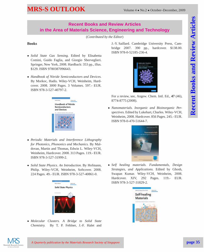
• Handbook of Nitride Semiconductors and Devices.By Morkoc, Hadis. Wiley-VCH, Weinheim, Hard-cover. 2008. 3000 Pages. 3 Volumes. 597.- EUR.ISBN 978-3-527-40797-2.
• Periodic Materials and Interference Lithographyfor Photonics, Phononics and Mechanics.By Mal-dovan, Martin and Thomas, Edwin L. Wiley-VCH,Weinheim, Hardcover. 2008. 313 Pages. 119.- EUR.ISBN 978-3-527-31999-2.
• Solid State Physics. An Introduction.By Hofmann,Philip. Wiley-VCH, Weinheim, Softcover. 2008.224 Pages. 49.- EUR. ISBN 978-3-527-40861-0.
ISBN 978-3-527-40861-0.
• Molecular Clusters. A Bridge to Solid StateChemistry. By T. P. Fehlner, J.-F. Halet and
J.-Y. Saillard. Cambridge University Press, Cam-bridge 2007. 390 pp., hardcover. $138.00.ISBN 978-0-52185-236-4.
For a review, see, Angew. Chem. Intl. Ed.,47 (46),8774-8775 (2008).
• Nanomaterials. Inorganic and Bioinorganic Per-spectives.Edited by Lukehart, Charles. Wiley-VCH,Weinheim, 2008. Hardcover. 856 Pages. 245.- EUR.ISBN 978-0-470-51644-7.
• Self healing materials. Fundamentals, DesignStrategies, and Applications.Edited by Ghosh,Swapan Kumar. Wiley-VCH, Weinheim, 2008.Hardcover. XIV, 292 Pages. 119.- EUR.ISBN 978-3-527-31829-2.
A Quarterly publication by the Materials Research Society of Singapore page 35

Volume 4• No.2• October–December, 2009 MRS-S OUTLOOKR
ecen
tBoo
ksan
dR
evie
wA
rtic
les
• Einstein Relation in Compound Semiconductorsand Their Nanostructures.By Kamakhya PrasadGhatak, Sitangshu Bhattacharya, and Debashis De.Springer, Berlin, 2008. Hardback: 477 pp., illus.$179.95. ISBN 9783540795568.
• High-Efficient Low-Cost Photovoltaics. RecentDevelopments.Edited by Vesselinka Petrova-Koch,Rudolf Hezel, and Adolf Goetzberger. Springer,Berlin, 2008. Hardback: 246 pp., illus. $149.95.ISBN 9783540793588.
• Piezoelectricity. Evolution and Future of a Technol-ogy.By Walter Heywang, Karl Lubitz, and WolframWersing. Springer, Berlin, 2008. Hardback: 600 pp.,illus. $189.95. ISBN 9783540686804.
• Self-Assembled Nanomaterials II: Nanotubes.Edited by Toshimi Shimizu. Springer, Berlin,2008. Hardback: 203 pp., illus. $229. ISBN9783540851042.
• Computational Multiscale Modeling of Fluids andSolids: Theory and Applications.By M. O. Stein-hauser. Springer, Berlin, 2008. Hardback: 445 pp.,illus. $159. ISBN 9783540751168.
• Introduction to Nanoelectronics: Science, Nan-otechnology, Engineering, and Applications.ByVladimir V. Mitin, Viatcheslav A. Kochelap, andMichael A. Stroscio. Cambridge University Press,Cambridge, 2008. Hardback: 345 pp., illus. $80.ISBN 9780521881722.
• The NMR Probe of High-Tc Materials.By R. E.Walstedt. Springer, Berlin, 2008. Hardback: 279 pp.,illus. $209. ISBN 9783540755647.
• Electronic Device Architectures for the Nano-CMOSEra. From Ultimate CMOS Scaling to BeyondCMOS Devices.Edited by Simon Deleonibus. PanStanford, Singapore, 2008. Hardback: 439 pp., illus.$167. ISBN 9789814241281.
• Mechanical Behavior of Materials.By Marc Andre
Meyers and Krishan Kumar Chawla, 2nd ed., Cam-bridge University Press, Cambridge, 2008. Hard-back: 880 pp., illus. $90. ISBN 9780521866750.
• Hydrogen Energy: Challenge and Prospects.By D.A. J. Rand and R. M. Dell, RSC Publishing, 2008,300 pp, Price£45, ISBN: 978-0-85404-597-6. For areview, see, J. Appl. Electrochem.,39(2), 311-312(2009).
• Introduction to Hydrogen Technology.By Roman J.Presset al.,. Wiley, Hoboken, NJ, 2008. Hardback:317 pp., $90. ISBN 9780471779858.
• Boulevard of Broken Symmetries. Effective FieldTheories of Condensed Matter.By Adriaan M.J. Schakel, World Scientific, Hackensack, NJ,2009. Hardback: 412 pp., illus. $79. ISBN9789812813909.
• Fundamentals of Photonic Crystal Guiding.ByMaksim Skorobogatiy and Jianke Yang, CambridgeUniversity Press, Cambridge, 2009. Hardback: 279pp., illus. $120. ISBN 9780521513289.
• Solution Processing of Inorganic Materials. Editedby Mitzi, David. Wiley-VCH, Weinheim, 2009.Hardcover. 498 Pages. Euro 105. ISBN-10: 0-470-40665-8. ISBN-13: 978-0-470-40665-6 — JohnWiley & Sons.
• Bulk Nanostructured Materials.Edited by Zehet-bauer, Michael J. and Zhu, Yuntian Theodore.Wiley-VCH, Weinheim, 2009. Hardcover. 710Pages. 199.- EUR. ISBN 978-3-527-31524-6.
A Quarterly publication by the Materials Research Society of Singaporepage 36
MRS-S OUTLOOK Volume 4• No.2• October–December, 2009
Rec
entB
ooks
and
Rev
iew
Art
icle
s
• Carbon Materials for Catalysis.Edited by Serp,Philippe and Figueiredo, Jose Luis. Wiley-VCH,Weinheim, 2009. Hardcover. 580 Pages. 125.-Euro. ISBN-10: 0-470-17885-X ISBN-13: 978-0-470-17885-0 - John Wiley & Sons.
• Computational Methods in Catalysis and MaterialsScience. An Introduction for Scientists and Engi-neers.Edited by van Santen, Rutger A., and Sautet,Philippe. Wiley-VCH, Weinheim, 2009. Hardcover.454 Pages. 99.- EUR. ISBN 978-3-527-32032-5.
• CVD Diamond for Electronic Devices and Sen-sors. Edited by Sussmann, Ricardo S. Wiley-VCH,Weinheim, 2009. Hardcover. 596 Pages. 175.- Euro.ISBN-10: 0-470-06532-X. ISBN-13: 978-0-470-06532-7 - John Wiley & Sons.
• Essentials of Modern Materials Science and Engi-neering.By Newell, James A. Wiley-VCH, Wein-heim, 2009. Softcover. 368 Pages. 47.9 Euro. ISBN-10: 0-471-75365-3. ISBN-13: 978-0-471-75365-0 -John Wiley & Sons.
• Chirality at the Nanoscale. Nanoparticles, Surfaces,Materials and more.Edited by Amabilino, DavidB. Wiley-VCH, Weinheim, 2009. Hardcover. 418Pages. 149.- Euro. ISBN-10: 3-527-32013-X. ISBN-13: 978-3-527-32013-4 - Wiley-VCH, Weinheim.
• Nanochemistry. A Chemical Approach to Nanoma-terials. By Geoffrey A. Ozin, Andre C. Arsenault,and Ludovico Cademartiri. 2nd Edition. RSC Pub-lishing, Cambridge, 2009. Hardback: 874 pp., illus.$89.95. ISBN 9781847558954.
A Quarterly publication by the Materials Research Society of Singapore page 37
Volume 4• No.2• October–December, 2009 MRS-S OUTLOOKR
ecen
tBoo
ksan
dR
evie
wA
rtic
les
• Computer Arithmetics for Nanoelectronics.By VladP. Shmerko, Svetlana N. Yanushkevich and SergeyEdward Lyshevski,CRC Press, Taylor and Francis Group, 2009. Hard-back. 408 pp., $129.95. ISBN: 9781420066210;ISBN 10: 1420066218.
• Nanotechnology. Volume 6: Nanoprobes.Edited byFuchs, Harald. Wiley-VCH, Weinheim, 2009. Hard-cover. 370 Pages. 149.- Euro. ISBN 978-3-527-31733-2.
• Science at the Nanoscale. An Introductory Textbook.By Chin Wee Shong, Sow Chorng Haur and AndrewT S Wee. Pan Stanford Publ. Pte. Ltd., Singapore,2009. 228 pp. US$88. ISBN 978-981-4241-03-8.
Review Articles
• High-Performance Organic Field-Effect Transistors.By D. Braga and G. Horowitz, Adv. Mater.,21(14-15), 1473-1486 (2009).
AbstractWith the advent of devices based on single crys-tals, the performance of organic field-effect transis-tors (OFETs) has experienced a significant leap, withmobility now in excess of 10 cm2 V−1 s−1. ThisReview gives an overview of the state-of-the-art of
these high-performance organic transistors. It alsofocuses on the problem of parameter extraction, lim-itations of the performance by the interfaces, whichinclude the dielectric-semiconductor interface, and theinjection and retrieval of charge carriers at the sourceand drain electrodes. 116 References.
• Toxicity Evaluation for Safe Use of Nanomaterials:Recent Achievements and Technical Challenges.ByS. M. Hussain, L. K. B.-Stolle, A. M. Schrand, R.C. Murdock, K. O. Yu, D. M. Mattie, J. J. Schlagerand M. Terrones, Adv. Mater.,21(16), 1549-1559(2009).
AbstractThis Review evaluates previous investigations relatedto nanomaterials (NM) toxicity studies using biologi-cal models and describes the limitations that often pre-vent toxicologists from identifying whether NM posea real hazard to human health. One major limitationto assess toxicity is the characterization of the NMprior to and after exposure to living cells or animals.The most relevant physicochemical characteristics ofNM are: size, surface chemistry, crystallinity, mor-phology, solubility, aggregation tendency, homogene-ity of dispersions, and turbidity. All of these proper-ties need to be assessed in order to determine theircontribution to toxicity. Due to the lack of appropri-ate methods to determine the physicochemical natureof nanoparticles in biological systems, the exact natureof NM toxicity is not fully described or understood atpresent. This Review emphasizes the need for state-of-the-art physicochemical characterization, the deter-mination of appropriate exposure protocols and reli-able methods for assessing NM internalization andtheir kinetics in living organisms. Once these issuesare addressed, optimal experimental conditions couldbe established in order to identify if NM pose a threatto human health. Multidisciplinary research betweenmaterials scientists and life scientists should overcomethese limitations in identifying the true hazards of NM.54 References.
• Developments of lithium-ion batteries and chal-lenges of LiFePO4 as one promising cathode mate-rial. By Z. Li, D. Zhang and F. Yang, J. Mater. Sci.,44 (10), 2435-2443(2009).
A Quarterly publication by the Materials Research Society of Singaporepage 38

MRS-S OUTLOOK Volume 4• No.2• October–December, 2009
Rec
entB
ooks
and
Rev
iew
Art
icle
s
AbstractDevelopments and developing trends of lithium-ionbatteries (LIBs) are summarized first: it is proposedthat solid thin film microbatteries and large-scale all-solid-state rechargeable LIBs are the two main devel-oping tendencies. Meanwhile, cost and safety issuesare the primary limitations to improve advanced LIBswith excellent electrochemical performance. Next, oneof the most promising cathode materials, LiFePO4,is introduced in detail. Advantages and drawbacks ofLiFePO4 as cathode active material are analyzed, andthe main approaches to circumvent its drawbacks pro-posed by many groups are also summarized. In addi-tion, some mechanism investigations carried out on thiscathode material, and challenging problems waiting forsolutions before LiFePO4 can be commercialized arealso discussed in this Review. 91 References.
• Recent Developments in the Field of InorganicPhosphors. By H. A. Hoppe, Angew Chem. Int. Ed.,48 (20), 3572-3582 (2009).
AbstractNew inorganic luminescent materials, especially thosedoped with rare earth ions can help to increaseenergy efficiency when used in plasma display panels(PDPs) and white-light-emitting diodes (white LEDs).In mercury-free fluorescent lamps these phosphorsmight contribute to environmental protection, and theyprovide better scintillation materials for medical diag-nostics. This Review focuses on some of the recentdevelopments. 131 References.
• Spider Silk: From Soluble Protein to ExtraordinaryFiber. By M. Heim, D. Keerl and T. Scheibel, AngewChem. Int. Ed.,48 (20), 3584-3596 (2009).
AbstractSpider silks have mechanical properties that outper-form most natural and synthetic fibers. In nature, theformation of a solid fiber from soluble spider silk pro-teins is the result of complex biochemical and physicalprocesses that take place within specialized spinningorgans. This review presents natural and artificial silkproduction processes, from gene transcription to silkprotein processing and finally fiber assembly. In-vivoand in-vitro findings in the field of spider silk research
form the basis for the design of new proteins and pro-cessing strategies, which will enable applications ofthese fascinating protein-based materials in technicaland medical sciences. 103 References.
• Magnesium nanostructures for energy storage andconversion. By B. Peng, J. Liang, Z. Tao and J.Chen, J. Mater. Chem.,19(19), 2877–2883 (2009).
AbstractMg nanostructures have enhanced the great potentialof bulk Mg in the area of energy storage and con-version due to their lightweight, abundant, and high-energy density properties. In this review, the authorshighlight the recent developments in the synthesis ofMg nanostructures and their application in two spe-cific areas: high-energy batteries and hydrogen storage(related to fuel cells). 64 References.
• Development of a roadmap for advanced ceramics:2010–2025. By J. Rodel, A. B.N. Kounga, M. W.-Eibl, D. Koch, A. Bierwisch, W. Rossner, M. J.Hoffmann, R. Danzer and G. Schneider, J. EuropeanCeram. Soc.,29 (9), 1549-1560 (2009).
AbstractA roadmap for advanced ceramics for the period from2010 to 2025 has been developed to provide guidelinesfor future investments for policy makers, scientists andindustry alike. Based on questionnaires, interviews anda final workshop with well-balanced participation ofmembers from industry and academia three roadmapson application fields, and two roadmaps on scientificareas have been developed and contrasted. The threeapplication fields selected are: (i) electronics, infor-mation and communication; (ii) energy and environ-ment; (iii) mechanical engineering, and the two scien-tific fields are: (a) structural and functional properties;(b) process technology.
These can be grouped into four major research top-ics which should be addressed in the future to securea sustainable development and growth of the advancedceramics markets: Novel ceramics with enhanced andnew properties; High-performance key components forsystem application; Highly efficient processing tech-nology; Holistic modelling and simulation techniques.
A Quarterly publication by the Materials Research Society of Singapore page 39

Volume 4• No.2• October–December, 2009 MRS-S OUTLOOKR
ecen
tBoo
ksan
dR
evie
wA
rtic
les
Within these topics, the tremendous growth opportuni-ties for ceramics as an enabling technology are high-lighted and manifold suggestions for future develop-ment are given. The authors conclude that increasinglymulti-disciplinary approaches and R&D co-operationswill be required. 46 References.
• Material and device considerations for organic thin-film transistor sensors. By M. E. Roberts, A. N.Sokolov and Z. Bao, J. Mater. Chem.,19 (21), 3351- 3363 (2009).
AbstractThe rapid development of the field of organic electron-ics has sparked great interest in the use of organic thin-film transistors (OTFTs) as low-cost electronic sen-sors. The direct coupling of the electronic and the sen-sor media to provide real time electrical output hasalready demonstrated high sensitivity to a variety ofchemical species. The synthetic versatility of organicmaterials also provides endless routes to impart func-tionality for specifically targeted chemical interactions.Owing to their compatibility with flexible materialsand simple fabrication methods, OTFTs are poised tohave a tremendous impact on future portable detectiontechnology. This article reviews recent progress madetoward improved sensitivity, selectivity and stability ofOTFT sensors through material and device engineer-ing. Specific consideration is paid to the interaction ofthe electronic materials with the analytes as a means ofproviding insight into mechanistic principles as well asthe future direction of OTFTs. 64 References.
• Conjugated Polyelectrolytes: Synthesis, Photo-physics, and Applications. By H. Jiang, P. Taranekar,J. R. Reynolds and K. S. Schanze, Angew. Chem.Int. Ed.,48 (24), 4300-4316 (2009).
AbstractConjugated polyelectrolytes (CPEs) are an emerg-ing class of multifunctional polymers that featureπ-conjugated backbones festooned with ionic solubiliz-ing groups. These materials have been exploited in anumber of applications, including fluorescent biosen-sors, polymer light-emitting diodes, and polymer solar
cells. CPEs provide a unique set of properties, includ-ing water solubility and processability, main-chain-controlled exciton and charge transport, variable bandgap light absorption and fluorescence, ionic interac-tions and aggregation phenomena. These characteris-tics allow them to be considered for use in applica-tions, like, light-emitting diodes, electrochromic color-changing displays, photovoltaic devices and photode-tectors, and chemical and biological sensors. ThisReview describes the evolution of CPE structures fromsimple polymers to complex materials, and illustrateshow the physical and electronic properties lead to use-ful applications in devices. 92 References.
• Thin-Film Transistors. By R. A. Street, Adv. Mater.,21(20), 2007-2022 (2009).
AbstractThin-film transistors (TFTs) matured later than sili-con (Si) integrated circuits, but in the past 15 yearsthe technology has grown into a huge industry basedon display applications, with amorphous and poly-crystalline Si as the incumbent technology. Recently,an intense search has developed for new materialsand new fabrication techniques that can improve theperformance, lower manufacturing cost, and enablenew functionality. There are now many new options,namely, organic semiconductors (OSCs), metal oxides,nanowires, printing technology as well as thin-film Simaterials with new properties. All of the new materialshave something to offer, but, according to the author,none is entirely without technical problems.80 Refer-ences.
• Reversible and High-Capacity Nanostructured Elec-trode Materials for Li-Ion Batteries. By M. G. Kimand J. Cho, Adv. Funct. Mater.,19(10), 1497-1514(2009).
AbstractReversible nano-structured electrode materials are atthe center of research relating to rechargeable lithiumbatteries, which require high power, high capacity,and high safety. The higher capacities and higher ratecapabilities for the nano-structured electrode materi-als in comparison to their bulk counterparts can beattributed to the higher surface area, which reduces
A Quarterly publication by the Materials Research Society of Singaporepage 40
MRS-S OUTLOOK Volume 4• No.2• October–December, 2009
Rec
entB
ooks
and
Rev
iew
Art
icle
s
the overpotential and allows faster reaction kinetics atthe electrode surface. These electrochemical enhance-ments can lead to versatile potential applications ofthe batteries and can provide breakthroughs for thecurrently limited power suppliers of mobile electron-ics. This Review describes recent research advances onnano-structured cathode and anode materials, such asmetals, metal oxides, metal phosphides and LiCoO2,Li(Ni 1−xMx)O2 with zero-, one-, two-, and three-dimensional morphologies. 147 References.
• Conducting-Polymer Nanomaterials for High-Performance Sensor Applications: Issues and Chal-lenges. By H. Yoon and J. Jang, Adv. Funct. Mater.,19(10), 1567-1576 (2009).
AbstractOwing to their promising applications in electronicand optoelectronic devices, conducting polymers havebeen continuously studied during the past few decades.Nevertheless, only limited progress had been madein conducting-polymer-based sensors until nanos-tructured conducting polymers were demonstratedfor high-performance signal transducers. Significantadvances in the synthesis of conducting-polymer nano-materials have been recently reported, with enhancedsensitivity relative to their bulk counterparts. Today,conducting-polymer nanomaterials rival metal andinorganic semiconductor nanomaterials in sensingcapability. However, there are still several techno-logical challenges to be solved for practical sensorapplications of conducting-polymer nanomaterials. Inthis Review article, the key issues on conducting-polymer nanomaterials in the development of state-of-the-art sensors are discussed. A perspective on next-generation sensor technology from a materials point ofview is also given. 73 References.
• Inorganic solid Li ion conductors: An overview. ByP. Knauth, Solid State Ionics,180 (14-16), 911-916(2009).
AbstractThis short review presents the state-of-the-art knowl-edge on crystalline, composite and amorphous inor-ganic solid lithium ion conductors (LICs), which areof interest as potential solid electrolytes in lithium
batteries and might replace the currently used poly-meric lithium ion conductors. The discussion of crys-talline LICs includes perovskite-type Lithium Lan-thanum Titanates, NASICON-type, LiSICON- andThio-LiSICON-type, as well as the garnet-type mixedoxides. The part on composite LICs discusses materialscontaining oxides and mesoporous oxides. In the amor-phous LIC part, mechanical attrition of Li-compounds,oxide and sulfide-based glasses as well as LIPON, andrelated systems are presented. 62 References.
• Complexity in biomaterials for tissue engineering.By E. S. Place, N. D. Evans and M. M. Stevens,Nature Mater.,8 (6),457-470 (2009).
AbstractThe molecular and physical information coded withinthe extracellular milieu is informing the developmentof a new generation of biomaterials for tissue engi-neering. Several powerful extracellular influences havealready found their way into cell-instructive scaffolds,while others remain largely unexplored. Yet, for com-mercial success tissue engineering products must benot only efficacious but also cost-effective, introducinga potential dichotomy between the need for sophistica-tion and ease of production. This is spurring interest inrecreating extracellular influences in simplified forms,from the reduction of biopolymers into short functionaldomains, to the use of basic chemistries to manipu-late cell fate. In the future these exciting developmentsare likely to help reconcile the clinical and commercialpressures on tissue engineering. 144 References.
• Ceramic technologies for automotive industry: Cur-rent status and perspectives. By A. Okada, Mater.Sci. & Engg.,B161(1-3) 182-187 (2009).
AbstractThe automotive industry has developed substantiallythrough advances in mechanical technologies, andtechnologies such as electronics and advanced materi-als have also contributed to further advances in auto-mobiles. The contribution of ceramic materials toautomobile technologies ranges over driving perfor-mance, exhaust gas purification, and fuel efficiencyimprovements. Several ceramic components, such as
A Quarterly publication by the Materials Research Society of Singapore page 41
Volume 4• No.2• October–December, 2009 MRS-S OUTLOOKR
ecen
tBoo
ksan
dR
evie
wA
rtic
les
knock sensors, oxygen sensors, exhaust gas cata-lysts, and silicon nitride parts for automotive engines,have been successfully applied to automobiles. ThisReview focuses on the contribution of ceramics toautomotive technologies. It also mentions potentialcontributions in the future, including adiabatic turbo-compound diesels, ceramic gas turbines, fuel cells, andelectric vehicles, because ceramic technologies havebeen intensively involved in the challenge to achieveadvanced power sources. 27 References.
• To What Extent Iron-Pnictide New Superconduc-tors Have Been Clarified: A Progress Report. By K.Ishida, Y. Nakai and H. Hosono, J. Phys. Soc. Japan,78 (6), 062001-1- 20 (2009).
AbstractThe discovery of the iron-based layered superconduc-tor, LaFeAs(O1−xFx) with a superconducting transi-tion temperature (Tc) ∼26 K by Kamiharaet al., in
2008 had a great impact to researchers in the areasof condensed-matter physics, solid state chemistry andmaterials science. Since then new iron-pnictide super-conductors with different crystal structures and varyingTc, namely, (Ba,K)Fe2As2), LiFeAs, and FeSe1−δhavebeen discovered and intensively investigated.
In this review, the authors present a summary ofexperimental reports on the iron-based superconduc-tors as they were known at the end of 2008. At thesame time, this paper is intended to be useful for exper-imenters to know the current status of these super-conductors. The authors introduce experimental resultsthat reveal basic physical properties in the normaland superconducting states. The similarities and differ-ences between iron-pnictide superconductors and otherunconventional superconductors are also discussed.123 References.
A Quarterly publication by the Materials Research Society of Singaporepage 42

MRS-S OUTLOOK Volume 4• No.2• October–December, 2009
The
me
Art
icle
Theme Article
From Applied Science to Commercial Application — Synchrotron Radiation as a Broad R&DPlatform: Part VIH. O. Moser1,2, K. Banas1, M. Cholewa1, C. Z. Diao1, X. Y. Gao2, L. K. Jian1, S. M. P. Kalaiselvi1, Z. J. Li1,G. Liu1, T. Liu2, S. K. Maniam1, A. T. S. Wee2, P. Yang1 and Y. Adam Yuan3,4
1Singapore Synchrotron Light Source, National University of Singapore, Singapore2Department of Physics, National University of Singapore, Singapore3Department of Biological Sciences, National University ofSingapore, Singapore4Temasek Life Sciences Laboratory, National University of Singapore and Nanyang Technological University, Singapore
[This is a six-Part article. Parts I-V appeared in the previous Issues. – Editor.]
8 Phase contrast imaging and tomography
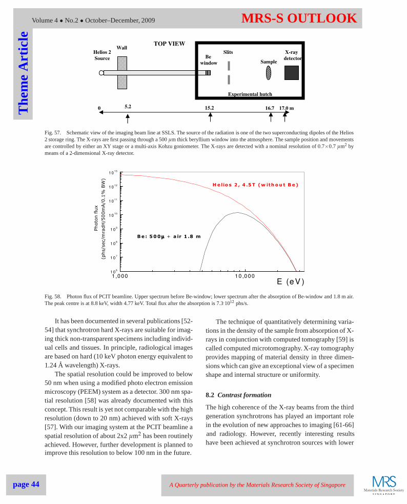
Over the past few years, results from the phase contrastimaging and tomography (PCIT) beamline [52-54] atthe Singapore Synchrotron Light Source (SSLS) haveshown that high resolution (about 2µm) 2-dimensional(2D) and 3-dimensional (3D) imaging can be achieved.Using white radiation the photon flux is high enoughto perform real time radiology (100 ms per frame) athigh lateral resolution as well as high-speed 2D imag-ing and 3D tomography. Refractive edge enhancementwas also observed. PCIT is mostly used for materialsand process characterization.
Although several groups [55, 56] have already doc-umented a resolution down to 20 nm with X-rays and3D tomography when imaging cryogenic single cellsand down to below 1 nm [57] with Transmission Elec-tron Microscopy (TEM), the useful sample sizes werelimited to less than a fewµm. However, there is a largepool of applications for which 1µm resolution tomog-raphy is optimal when sample sizes approach 1-2 mm.In this paper, we concentrate on selected applicationsat about 1µm resolution. Additionally, a new project atSSLS will be discussed for reaching a resolution downto 50 nm.
8.1 Experimental set up
The schematic diagram of the PCIT beamline is pre-sented in Fig. 57. PCIT is a simple beam line devotedto imaging. It features a fast valve, ion pumps, a rect-angular wall through tube, aγ-shutter and a Be win-dow at the end. At present it offers a white beam ofhard X-rays with a cross section of 20x8 mm2 and
energy range of about 2 – 15 keV. Source parame-ters are as follows:σx =0.76 mm,σy =0.38 mm,σx’=2.56 mrad,σy’ =0.06 mrad. The system is designed
to produce a beam of about 1x1 mm2 at the samplewith the use of variable slits. The X-ray beam is deliv-ered from the Helios 2 storage ring without any focus-ing and monochromatisation.After passing through the500 µm thick Be window and about 1.5 m of air thebeam is collimated at the specimen. Spectra of X-raysas emerging from the Helios 2 ring and as at the sampleposition are shown in fig. 58. After passing through thespecimen, X-rays are converted to visible photons bya thin (ca. 300µm thick) CdWO4 scintillator and laterdetected by the Roper Scientific CoolSNAP cf CCDcamera with 1,392×1,040 pixels. A×5 objective isused to magnify the beam from the mirror to the CCDcamera. The CoolSNAP cf CCD camera is equippedwith a 7.2×6.2 mm2 size CCD chip and operates at 25Megapixels per second. This is the 12-bit camera withaverage speed of 17.3 frames per second of readouttime. Its noise level of 15e- is quite high, but sufficientfor most experiments performed. The increase of theimage size by the×5 objective determines the effectivesize of the image to 976×728µm2 and nominal pixelresolution of 0.7× 0.7µm2. Although SSLS has a bril-liance of 3× 10¹² photons/mm2/mrad2/0.1% BW at 6keV that is up to three orders of magnitude smaller thanthat of 3rd generation synchrotron light sources, use ofbroadband radiation enables the flux of X-rays at thesample to be sufficient to perform high speed experi-ments including 2D imaging and 3D tomography.
A Quarterly publication by the Materials Research Society of Singapore page 43
Volume 4• No.2• October–December, 2009 MRS-S OUTLOOKT
hem
eA
rtic
le
TOP VIEW
Helios 2
Source
Wall X-ray
detector
5.2 0 15.2 16.7 17.0 m
Be
window Sample
Experimental hutch
Slits
Fig. 57. Schematic view of the imaging beam line at SSLS. The source of the radiation is one of the two superconducting dipoles of the Helios2 storage ring. The X-rays are first passing through a 500µm thick beryllium window into the atmosphere. The sample position and movementsare controlled by either an XY stage or a multi-axis Kohzu goniometer. The X-rays are detected with a nominal resolution of 0.7×0.7µm2 bymeans of a 2-dimensional X-ray detector.
1,0 00 10 ,0 0 01 0
6
1 07
1 08
1 09
1010
1011
1012
1013
Be : 500 µµµµ + a ir 1 .8 m
He lio s 2 , 4 .5T (w ithou t B e)
Photon flux
(phs/sec/mradH/500mA/0.1% BW)
E (eV )
Fig. 58. Photon flux of PCIT beamline. Upper spectrum before Be-window; lower spectrum after the absorption of Be-windowand 1.8 m air.The peak centre is at 8.8 keV, width 4.77 keV. Total flux after the absorption is 7.3.1012 phs/s.
It has been documented in several publications [52-54] that synchrotron hard X-rays are suitable for imag-ing thick non-transparent specimens including individ-ual cells and tissues. In principle, radiological imagesare based on hard (10 keV photon energy equivalent to1.24A wavelength) X-rays.
The spatial resolution could be improved to below50 nm when using a modified photo electron emissionmicroscopy (PEEM) system as a detector. 300 nm spa-tial resolution [58] was already documented with thisconcept. This result is yet not comparable with the highresolution (down to 20 nm) achieved with soft X-rays[57]. With our imaging system at the PCIT beamline aspatial resolution of about 2x2µm2 has been routinelyachieved. However, further development is planned toimprove this resolution to below 100 nm in the future.
The technique of quantitatively determining varia-tions in the density of the sample from absorption of X-rays in conjunction with computed tomography [59] iscalled computed microtomography. X-ray tomographyprovides mapping of material density in three dimen-sions which can give an exceptional view of a specimenshape and internal structure or uniformity.
8.2 Contrast formation
The high coherence of the X-ray beams from the thirdgeneration synchrotrons has played an important rolein the evolution of new approaches to imaging [61-66]and radiology. However, recently interesting resultshave been achieved at synchrotron sources with lower
A Quarterly publication by the Materials Research Society of Singaporepage 44

MRS-S OUTLOOK Volume 4• No.2• October–December, 2009
The
me
Art
icle
(A) (B)
A
100 µm 100 µm
Fig. 59. Two-dimensional image of 70µm diameter nylon fibre (A) and calculated phase (B). White lines of edge enhancement clearly visibleat the edge of a fibre at image A. Phase images have been calculated by Tim Gureyev from CSIRO in Melbourne, Australia.
coherence [52,54]. In these works, it was documentedthat combination of refraction and diffraction effectscould produce an edge enhancement and improvementin the image quality. It was shown that without highspace and time coherence an enhancement in the phasecontrast imaging is possible. This well documentedexperimental work had been supported recently by the-oretical calculations [67]. The formation of the imageat the PCIT beamline includes a combination of effectssuch as absorption, reflection, refraction and diffrac-tion.
In the complex X-ray refractive index n = 1 -δ - iβ,the absorption contrast is related to the imaginary com-ponent iβ, while the real componentδ is closely relatedto phase contrast imaging (PCI). Many examples ofPCI will involve a combination of phase and absorp-tion contrast to varying degrees. While both generallydecrease with increasing X-ray energy, it is importantto note thatδ varies asλ2 whereasβ varies asλ4,whereλ is the wavelength of X-rays.
Detailed studies of contrast mechanisms includingmeasurements of partial coherence of the beam, refrac-tion, diffraction and absorption are under way. Fig.59A represents a 2D image collected from a 70µmdiameter nylon fibre. Fig. 59B represents a 2D phasedistribution of the nylon fibre from the image.
8.3 Results and conclusions
In one of the first demonstrations of the X-ray micro-tomography at SSLS, we used the water filtration fibre.A straight section of the fibre was selected for the CATscan. For the X-ray microtomography, each projectionwas made by detecting the beam of X-rays passing
through the sample (approximately∼1×1 mm2 ). Thesample was rotated by 0.18◦ between each projection.Typically up to 1,000 projections over 180◦ are beingcollected during a 2 hours’ scan. The beam of X-raysexperienced sufficient refraction to give good contrastat micron resolution.
1,000 projections were collected during the experi-ment with 2 seconds per projection. Each projection isa 2D image with 1,392×1,040 pixels and 12-bit accu-racy (ca. 2.83 Mb per image). Collected data wereanalyzed with the specially developed software andthe image reconstructed using filtered backprojectionalgorithm. The estimated spatial resolution after recon-struction was about 2µm. Individual reconstructedslices are presented in Fig. 60. By putting many recon-structed slices together we were able to display 3-dimensional details of the specimen with∼2 µm reso-lution in all three directions as shown in Fig. 60.
A group of Prof. Hutmacher from Faculty of Engi-neering at National University of Singapore (NUS)has been developing artificial scaffolds. The combi-nation of bioactive ceramics like calcium phosphateswith polymers improves the mechanical properties ofthe composite and enhances the osteoconductive prop-erties of the polymer. Polymers have been added tocalcium phosphate materials in order to improve theirmechanical strength and calcium phosphate fillers havebeen blended with polymers to improve their compres-sive strength and modulus. Such samples are not trans-parent and could only be visualized in 3D using micro-tomography technique at SSLS. The result is shown inFig. 61.
A Quarterly publication by the Materials Research Society of Singapore page 45

Volume 4• No.2• October–December, 2009 MRS-S OUTLOOKT
hem
eA
rtic
le
A B
100 µm
Fig. 60. Reconstructed slice which shows the internal structure of a water filtration fibre made of poly acrylonitrile. A)shows a recon-structed slice from the fibre before the filtration process. B) shows a reconstructed 3D image of the water filtration fibre.This image comprises976×976×728µm3.
Fig. 61. Reconstructed 3D view which shows the internal structure of an artificial scaffold made of polycaprolactone – tricalcium phosphate(PCL – TCP) polymer matrix with CaP particles (red color). This image comprises 976×976×728µm3.
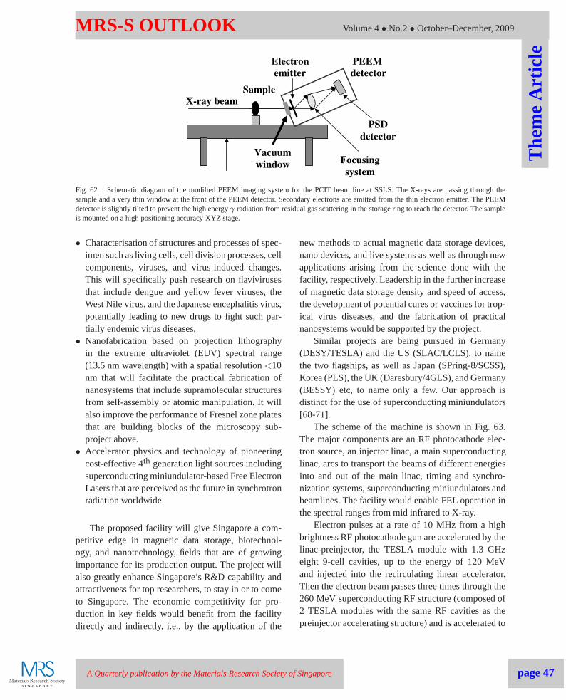
SSLS is working at improving the spatial res-olution to below 50 nm by modifying a standardphoto electron emission microscopy (PEEM) system todevelop the XEEM microscope. A 300 nm spatial reso-lution [58] was already demonstrated with this concept.A further reduction to the sub 10 nm range may be pos-sible using a proposed time-of-flight PEEM approach[60]. The proposed upgrading of the PCIT beam linewith the modified PEEM imaging system is shownschematically in Fig. 62.
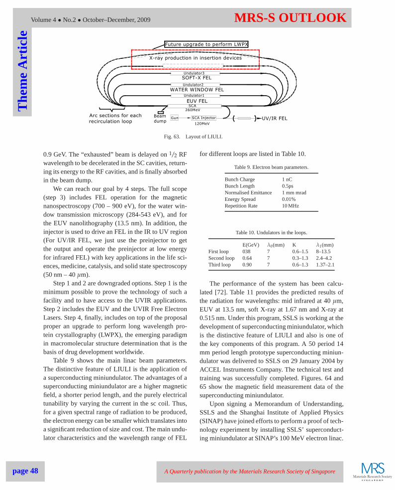
9 LIULI – A leading facility for Singaporescience
Besides the exploitation of the Helios 2 superconduct-ing compact storage ring for user operations and forits own R&D work, SSLS envisions a 4th generationsynchrotron light source to complement and, eventu-ally, replace the current facility. This vision includes an
accelerator system based on a superconducting linearaccelerator with up to 5 recirculation loops for energymultiplication and recovery with the distinguishingfeature that the light would be generated by super-conducting mini- and micro-undulators. The respec-tive R&D programme is called LIULI which standsfor LInac Undulator Light Installation. This facilitywould position Singapore among the leading playersin photon science. It aims at the solution of three keyproblems in nanotechnology and the life sciences. Theproject will set new standards in the
• Characterization of magnetic structures by nanospectroscopy and nano imaging on the<2 nm reso-lution level including element-specific and chemicalcontrast for the benefit of basic science, technologi-cal applications, as well as commercial exploitation,
A Quarterly publication by the Materials Research Society of Singaporepage 46
MRS-S OUTLOOK Volume 4• No.2• October–December, 2009
The
me
Art
icle
X-ray beamSample
PEEM
detector
Electron
emitter
Vacuum
window
PSD
detector
Focusing
system
Fig. 62. Schematic diagram of the modified PEEM imaging system for the PCIT beam line at SSLS. The X-rays are passing through thesample and a very thin window at the front of the PEEM detector. Secondary electrons are emitted from the thin electron emitter. The PEEMdetector is slightly tilted to prevent the high energyγ radiation from residual gas scattering in the storage ring to reach the detector. The sampleis mounted on a high positioning accuracy XYZ stage.
• Characterisation of structures and processes of spec-imen such as living cells, cell division processes, cellcomponents, viruses, and virus-induced changes.This will specifically push research on flavivirusesthat include dengue and yellow fever viruses, theWest Nile virus, and the Japanese encephalitis virus,potentially leading to new drugs to fight such par-tially endemic virus diseases,
• Nanofabrication based on projection lithographyin the extreme ultraviolet (EUV) spectral range(13.5 nm wavelength) with a spatial resolution<10nm that will facilitate the practical fabrication ofnanosystems that include supramolecular structuresfrom self-assembly or atomic manipulation. It willalso improve the performance of Fresnel zone platesthat are building blocks of the microscopy sub-project above.
• Accelerator physics and technology of pioneeringcost-effective 4th generation light sources includingsuperconducting miniundulator-based Free ElectronLasers that are perceived as the future in synchrotronradiation worldwide.
The proposed facility will give Singapore a com-petitive edge in magnetic data storage, biotechnol-ogy, and nanotechnology, fields that are of growingimportance for its production output. The project willalso greatly enhance Singapore’s R&D capability andattractiveness for top researchers, to stay in or to cometo Singapore. The economic competitivity for pro-duction in key fields would benefit from the facilitydirectly and indirectly, i.e., by the application of the
new methods to actual magnetic data storage devices,nano devices, and live systems as well as through newapplications arising from the science done with thefacility, respectively. Leadership in the further increaseof magnetic data storage density and speed of access,the development of potential cures or vaccines for trop-ical virus diseases, and the fabrication of practicalnanosystems would be supported by the project.
Similar projects are being pursued in Germany(DESY/TESLA) and the US (SLAC/LCLS), to namethe two flagships, as well as Japan (SPring-8/SCSS),Korea (PLS), the UK (Daresbury/4GLS), and Germany(BESSY) etc, to name only a few. Our approach isdistinct for the use of superconducting miniundulators[68-71].
The scheme of the machine is shown in Fig. 63.The major components are an RF photocathode elec-tron source, an injector linac, a main superconductinglinac, arcs to transport the beams of different energiesinto and out of the main linac, timing and synchro-nization systems, superconducting miniundulators andbeamlines. The facility would enable FEL operation inthe spectral ranges from mid infrared to X-ray.
Electron pulses at a rate of 10 MHz from a highbrightness RF photocathode gun are accelerated by thelinac-preinjector, the TESLA module with 1.3 GHzeight 9-cell cavities, up to the energy of 120 MeVand injected into the recirculating linear accelerator.Then the electron beam passes three times through the260 MeV superconducting RF structure (composed of2 TESLA modules with the same RF cavities as thepreinjector accelerating structure) and is accelerated to
A Quarterly publication by the Materials Research Society of Singapore page 47
Volume 4• No.2• October–December, 2009 MRS-S OUTLOOKT
hem
eA
rtic
le
Arc sections for each
recirculation loopBeam
dump
X-ray production in insertion devices
Future upgrade to perform LWPX
UV/IR FEL
WATER WINDOW FEL
SOFT-X FEL
EUV FEL
260MeV
120MeV
SCA InjectorGun
Undulator3
Undulator2
Undulator1
SCA
Fig. 63. Layout of LIULI.
0.9 GeV. The “exhausted” beam is delayed on1/2 RFwavelength to be decelerated in the SC cavities, return-ing its energy to the RF cavities, and is finally absorbedin the beam dump.
We can reach our goal by 4 steps. The full scope(step 3) includes FEL operation for the magneticnanospectroscopy (700 – 900 eV), for the water win-dow transmission microscopy (284-543 eV), and forthe EUV nanolithography (13.5 nm). In addition, theinjector is used to drive an FEL in the IR to UV region(For UV/IR FEL, we just use the preinjector to getthe output and operate the preinjector at low energyfor infrared FEL) with key applications in the life sci-ences, medicine, catalysis, and solid state spectroscopy(50 nm – 40µm).
Step 1 and 2 are downgraded options. Step 1 is theminimum possible to prove the technology of such afacility and to have access to the UVIR applications.Step 2 includes the EUV and the UVIR Free ElectronLasers. Step 4, finally, includes on top of the proposalproper an upgrade to perform long wavelength pro-tein crystallography (LWPX), the emerging paradigmin macromolecular structure determination that is thebasis of drug development worldwide.
Table 9 shows the main linac beam parameters.The distinctive feature of LIULI is the application ofa superconducting miniundulator. The advantages of asuperconducting miniundulator are a higher magneticfield, a shorter period length, and the purely electricaltunability by varying the current in the sc coil. Thus,for a given spectral range of radiation to be produced,the electron energy can be smaller which translates intoa significant reduction of size and cost. The main undu-lator characteristics and the wavelength range of FEL
for different loops are listed in Table 10.
Table 9. Electron beam parameters.
Bunch Charge 1 nCBunch Length 0.5psNormalised Emittance 1 mm mradEnergy Spread 0.01%Repetition Rate 10 MHz
Table 10. Undulators in the loops.
E(GeV) λ0(mm) K λ1(mm)First loop 038 7 0.6–1.5 8–13.5Second loop 0.64 7 0.3–1.3 2.4–4.2Third loop 0.90 7 0.6–1.3 1.37–2.1
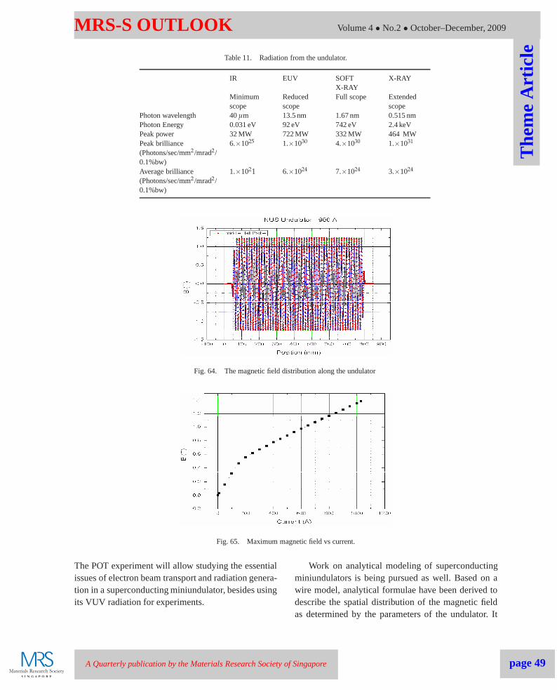
The performance of the system has been calcu-lated [72]. Table 11 provides the predicted results ofthe radiation for wavelengths: mid infrared at 40µm,EUV at 13.5 nm, soft X-ray at 1.67 nm and X-ray at0.515 nm. Under this program, SSLS is working at thedevelopment of superconducting miniundulator, whichis the distinctive feature of LIULI and also is one ofthe key components of this program. A 50 period 14mm period length prototype superconducting miniun-dulator was delivered to SSLS on 29 January 2004 byACCEL Instruments Company. The technical test andtraining was successfully completed. Figures. 64 and65 show the magnetic field measurement data of thesuperconducting miniundulator.
Upon signing a Memorandum of Understanding,SSLS and the Shanghai Institute of Applied Physics(SINAP) have joined efforts to perform a proof of tech-nology experiment by installing SSLS’ superconduct-ing miniundulator at SINAP’s 100 MeV electron linac.
A Quarterly publication by the Materials Research Society of Singaporepage 48
MRS-S OUTLOOK Volume 4• No.2• October–December, 2009
The
me
Art
icleTable 11. Radiation from the undulator.
IR EUV SOFTX-RAY
X-RAY
Minimumscope
Reducedscope
Full scope Extendedscope
Photon wavelength 40µm 13.5 nm 1.67 nm 0.515 nmPhoton Energy 0.031 eV 92 eV 742 eV 2.4 keVPeak power 32 MW 722 MW 332 MW 464 MWPeak brilliance(Photons/sec/mm2 /mrad2/0.1%bw)
6.×1025 1.×1030 4.×1030 1.×1031
Average brilliance(Photons/sec/mm2 /mrad2/0.1%bw)
1.×1021 6.×1024 7.×1024 3.×1024
Fig. 64. The magnetic field distribution along the undulator
Fig. 65. Maximum magnetic field vs current.
The POT experiment will allow studying the essentialissues of electron beam transport and radiation genera-tion in a superconducting miniundulator, besides usingits VUV radiation for experiments.
Work on analytical modeling of superconductingminiundulators is being pursued as well. Based on awire model, analytical formulae have been derived todescribe the spatial distribution of the magnetic fieldas determined by the parameters of the undulator. It
A Quarterly publication by the Materials Research Society of Singapore page 49
Volume 4• No.2• October–December, 2009 MRS-S OUTLOOKT
hem
eA
rtic
le was shown that the location of the field zeros is shiftedcompared with the position of the wires. This finite-length field error is systematic and alters the radia-tion spectrum significantly. After introducing a sim-ple compensation coil, the field quality, locations ofzeros, field integrals, and radiation spectrum becomesatisfactory [73]. Semi-analytical and numerical simu-lations are performed to estimate the tolerances of var-ious errors required for a satisfactory function of thesuperconducting miniundulator, including the effectsof systematic errors such as pitch, yaw and roll errorsof a whole superconducting miniundulator coil, andrandom errors of the wire positions [74].
Acknowledgement
Work supported in part by NUS Core SupportC-380-003-003-001, A*STAR/MOE RP 3979908M,A*STAR 012 105 0038, A*STAR R144-000-053-303,ARF R-144-000-53-107, and A*STAR 012 101 0131grants. Concerning HRXRD, we are grateful to GaoXinsheng, Tim White, Ooi Soo Ting, Yuan Hairong,Dong Jianrong, L.C. Lim, W.S. Chang and Wen Li forproviding samples or results. Regarding XRR, we aregrateful to P. Darmawan, P. S. Lee, Lin Qidan, D. Lu,B. Ramana Murthy, Low Hong Yee, Guo Qiang andD.H. Kim for providing samples.
References
52. W.L. Tsai, H.M. Chang, Y. Hwu, P.C. Hsu, H.L. Tsai,G.M. Chow, P.C. Ho, S.C. Li, H.O. Moser, Y. Ping, S.K.Seol, H. Je, A. Groso and G. Margaritondo, Imaging cellswith refractive index radiology,Biophysical Journal87,4180-4187(2004).
53. A. Yeo, P. Yang, A.G. Fane, T. White and H.O. Moser,Noninvasive observation of external and internal depo-sition during membrane filtration by X-ray Microimag-ing (XMI), Journal of Membrane Science250, 189-193(2005).
54. W.L. Tsai, P.C. Hsu, Y. Hwu, J.H. Je, P. Yang, H.O.Moser, A. Groso and G. Margaritondo, Edge-enhanced
radiology with broadband synchrotron X-rays, in H.O.Moser, ed., Synchrotron Radiation in Materials Science(SRMS-3),Nucl. Instr. and Meth.B199, 436-440(2003).
55. D. Weiss, G. Schneider, B. Niemann, P. Guttmann,D. Rudolph and G. Schmahl,Ultramicroscopy 84,185(2000).
56. M.A. Le Gros, G. McDermott and C.A. Larabell,CurrentOpinion in Structural Biology15,593-600(2005).
57. U. Ziese, C. Kubel. A.J. Verkleij and A.J. Koster,J. ofStruct. Biology138,58-62(2002).
58. Y. Hwu, W.L. Tsai, B. Lai, J.H. Je, G.H. Fecher, M.Bertolo and G. Margaritondo, Using photoelectron emis-sion microscopy with hard X-rays,Surface Science480,188-195(2001).
59. E. Seeram, Computed tomography, W.B Saunders(2001).
60. A. Khursheed,J. Vac. Sci. Technol. B23, 2749-2753(2005).
61. G. Margaritondo,Phys. World11,28(1998).62. A. Snigirev, I. Snigireva, V. Kohn, S. Kuznetsov and I.
Schelokov,Rev. Sci. Instr.66,5486-5492 (1995).63. A. Pogany, D. Gao and S.W. Wilkins,Rev. Sci. Instr.68,
2774-2782 (1997).64. K.A. Nugent, T.E. Gureyev, D.F. Cookson, D. Paganin
and Z. Barnea,Phys. Rev. Lett.77,2961-2964 (1996).65. K.A. Nugent, A.G. Peele, H.M. Quiney and H.N. Chap-
man,Acta Cryst. A61,373-381 (2005).66. K.A. Nugent, A.G. Peele, H.N. Chapman and A.P. Man-
cuso,Phys. Rev. Lett.91,203902(1-4) (2003).67. Ya. I. Nesterets, S.W. Wilkins, T.E. Gureyev, A. Pogany
and A.W. Stevenson,Rev. Sci. Instr.76, (2005).68. H.O. Moser, B. Krevet and H. Holzapfel, Mikroundula-
tor, German patent P 41 01 094.9-33, Jan. 16, 1991.69. G. Ingold, I. Ben-Zvi, L. Solomon and M. Woodle,Nucl.
Instr. Meth. A375,451(1996).70. S. Casalbuoni, M. Hagelstein, B. Kostka and R. Ross-
manith, Physical Review ST-Accelerator and Beams9,010702 (2006).
71. H.O. Moser and C.Z. Diao,International Journal ofModern Physics B21,508-512(2007).
72. Ming Xie, IEEE Proceedings for PAC95, No.95CH3584,183, 1996.
73. H.O. Moser and C.Z. Diao,Nucl. Instr. Meth. A535,606-613(2004).
74. C.Z. Diao and H.O. Moser,RRCAT, Indore, India, 711-713 (2007).
A Quarterly publication by the Materials Research Society of Singaporepage 50
Proceedings of APAC07,
MRS-S OUTLOOK Volume 4• No.2• October–December, 2009
The
me
Art
icle
is the Director of the Singapore Synchrotron
ingapore, since
t of
ical diagnostics
gszentrum
radiation in
He pioneered
diation facility
strongly
Herbert O. Moser is the Director of the Singapore Synchrotron Light Source (SSLS) at theNational University of Singapore, since 2000, and a Professor of Physics with the Departmentof Physics/NUS. After 15 years of acceleration and optical diagnostics of cluster ion beamsfor nuclear fusion at Forschungszentrum Karlsruhe (FZK), he joined the field of synchrotronradiation in 1983, working on both, generation and applications. He pioneered and led theconstruction of the ANKA synchrotron radiation facility atFZK including the development ofsuperconducting miniundulators. Under his leadership, SSLS has been strongly promoting bothscientific and commercial use of synchrotron radiation. H.O. Moser’s current research interests
include micro/nanomanufactured electromagnetic metamaterials and optical/photonics devices, X-ray phase con-trast and coherent diffraction imaging, reflectometry and diffraction, forensics, superconducting miniundulators,and accelerators. He has more than 280 publications, 15 patents and 7 more in the pipeline. He is Editor-in-Chiefof Advances in Synchrotron Radiation.
apore
gapore since 2008.
Doctorate (Ph.D.) in
the Jagiellonian
Postdoctoral
004-2006 he worked
of Sciences in Cracow,
Fast and accurate
in the
ed by the Prime
Krzysztof Banashas been working as the beamline scientist at Singapore Synchrotron LightSource National University of Singapore since 2008. He received his Diploma (M.Sc.) inPhysics and his Doctorate (Ph.D.) in Physics, in 1996 and 2002, respectively, both from theJagiellonian University in Cracow, Poland. In 2002-2004 hewas a Postdoctoral Researcher atUniversity of Leipzig, Germany. In 2004-2006 he worked at the Institute of Nuclear PhysicsPolish Academy of Sciences in Cracow, Poland. In 2007 he was co-worker in project enti-tled Fast and accurate characterization of explosives by means of synchrotron radiationinthe frame of The Enterprise Challenge Program established by the Prime Minister’s Office of
the Government of the Republic of Singapore. His research interests include various imaging and spectroscopictechniques, application of multivariate statistical analysis and digital signal processing for data evaluation.
Marian Cholewa has been working as the Beamline Senior Research Fellow at Monash Uni-versity, Australia since 2008. He received his Diploma (M.Sc.) in Physics from the JagiellonianUniversity in Cracow, Poland in 1977. He received his Doctorate (Ph.D.) in Physics and habil-itation in Physics, in 1987 and 2007, respectively, both from the Institute of Nuclear PhysicsPolish Academy of Sciences in Cracow, Poland. Since 1977 he has been working at scientific
institutions in Poland (1977-1987), USA (1982-1985), Australia (1987-1998), Germany (2000-2003 and 2007-2008) and Singapore (2003-2007). And he had been a Director of MC Scientific Consulting (1998-2004). Hisresearch interests include various development and applications of imaging, spectroscopic techniques and livecells irradiation with high resolution microbeams. He is anauthor or co-author of over 120 publications in thescientific journals. He has been a recipient of several research grants in Australia and overseas. And is an author of2 patents.
A Quarterly publication by the Materials Research Society of Singapore page 51

Volume 4• No.2• October–December, 2009 MRS-S OUTLOOKT
hem
eA
rtic
le
Diao Caozhengreceived Ph. D. degree from the University of Science and Technology ofChina (USTC) in 1998. From 1995 to 2001, he has participated in the design, commission-ing of the storage ring FEL at NSRL in China. From 2001 to 2003,he worked at SCA-FEL,Stanford University on the development of an IR-FEL. Since 2003, he joined SSLS to work atmachine group and research work on the development of superconducting miniundulator and
the conceptual design of a new light source (LIULI).
Xingyu Gao completed his B. Sc. from Peking University in July 1991 and M.Sc. fromPeking University in July 1994. He completed his Dr. rer. nat. from Max-Planck-Institute forMicrostructure physics and Martin-Luther University in Germany in 1999. From June 2000 toFeb 2002, he worked as a postdoctoral associate in Department of Physics of Louisiana StateUniversity in USA. From Feb 2002 to present, he worked as a research fellow in Department ofPhysics, National University of Singapore. He was promotedto senior research fellow in 2007.He has authored or co-authored over 70 Scientific Publications in peer-reviewed journals. Hisresearch interests include surface physics, material science, ultra-thin films especially organic
and magnetic films, nano structures, synchrotron radiationrelated techniques, and first-principle calculation.
Jian Linke obtained his Bachelor, Master and Ph D. degree (1989) from Xian Jiaotong Univer-sity, China, major in Mechanical Engineering. From 2005, hehas been working in SingaporeSynchrotron Light Source, National University of Singapore, as head of Micro-Nanofabricationgroup. Before joining the SSLS/NUS, he has worked in Department of Mechanical Engineer-ing, Xian Jiaotong University, China (1989-1998); in Center for Advanced Microstrucrures andDevice (CAMD), Louisiana University (LSU), USA (1998-2002) and in Application Center forMicroengineering, BESSY GmbH, Berlin, Germany (2002-2005). His research work is mainlyon the area of micro/nanofabrication by means of e-beam writing, laser writing, optical and
X-ray lithography as well as LIGA (lithography, electroplating and molding) process.
S. M. Kalaiselvi obtained her Bachelor of Engineering degree from Madras University, Indiain the year 2001, specializing in Electronics and Instrumentation, and her Master of Sci-ence degree from Nanyang Technological University, Singapore in the year 2006, major-ing Photonics. She is currently working at Singapore Synchrotron Light Source, NUS, sinceJanuary 2007, at the fabrication of freely-suspended matrix-free THz electromagnetic meta-materials composed of upright S structures using three level aligned lithography (Metafoil). Her job scope involves Deep X-ray lithography, UV Lithography, Mask designing& Fabrication, Metrology (Optical microscopy, Wyko profiling, SEM), RIE, DC and RFsputtering, DC and pulsed plating of Gold and Ni, FTIR spectroscopy, hot Embossing and
Simulation using CST-Microwave studio.
A Quarterly publication by the Materials Research Society of Singaporepage 52

MRS-S OUTLOOK Volume 4• No.2• October–December, 2009
The
me
Art
icle
After completing her undergraduate studies at Tianjin University in 1992, MsLi Zhi Juangraduated from Beijing Jiaotong University, China, with M.S in Optics in 1997. She workedas a technical support staff at Krystal International Ltd inBeijing since her graduation. Shethen resided in USA for a while but returned to China and joined Tiger Technology Limitedin Shijiazhuang as a project manager in June 2002. She oversaw a G2 project involving real-time intelligent expert and neural network systems used in fermentation of penicillin in a NorthChina pharmaceutical factory. Zhi Juan came to Singapore inlate 2005 to join SSLS, NUS
as a Research Assistant, working at the PCIT beamline and on the X-ray technique analysis of different kind ofexplosive materials project. She left for Germany in 2007 towork on her PhD studies at ISS, FZK, majoring inrocking curve X-ray imaging technique.
Gang Liu received the B.S. degree in organic chemistry from Anhui University, Anhui, China,in 1993, and the Ph.D. degree in application of synchrotron radiation from the University ofScience and Technology of China (USTC), Hefei, China, in 2002. He is an Associate Professorin the National Synchrotron Radiation Laboratory, USTC. Hehas worked for one year (2007)in micro/nanofabrication group of SSLS. He is currently working on synchrotron radiationapplications and associated LIGA and UV-LIGA technologies.
T. Liu A staff member at Institute for Synchrotron Radiation, Forschungszentrum Karl-sruhe, Germany; 10/2007∼4/2008: research fellow at Singapore Synchrotron Light Source,National University of Singapore; 06/2005∼09/2007: research fellow at Department ofPhysics, National University of Singapore; 01/1998∼06/2005: beamline scientist at Syn-chrotron Radiation Laboratory, Institute of High Energy Physics, Chinese Academy of Sci-ences, Beijing; 11/2000∼05/2002: visiting scientist at Chemistry Division, Argonne NationalLaboratory, Argonne, USA.
Sivakumar M. Maniam received the B. App. Sc.(Hons) in physics from University SainsMalaysia, Malaysia, and MSc. in Photonics from Nanyang Technological University, Singa-pore, in 1999 and 2007, respectively. He worked as an equipment engineer in the semiconduc-tor and analytical industry for 5 years. He is currently a Research Assistant with SingaporeSynchrotron Light Source (SSLS), National University of Singapore, and member of Electro-magnetic Metamaterial and Lithography for Micro- and Nano Technology group in SSLS. Cur-
rent research interest includes in nanostructure metamaterials and graphene. Mr. Maniam is a Member of Instituteof Physics (UK) and Material Research Society of Singapore.He is also currently a graduate student in Departmentof Physics and Centre for Quantum Technologies, NUS, working on disorder in graphene lattice.
A Quarterly publication by the Materials Research Society of Singapore page 53

Volume 4• No.2• October–December, 2009 MRS-S OUTLOOKT
hem
eA
rtic
le
Andrew Weeobtained his BA and MA (Physics) from the University of Cambridge, and DPhilfrom the University of Oxford, UK. He is a Professor of Physics at the National University ofSingapore (NUS), and currently Dean, Faculty of Science. Hehas published more than 300papers in internationally refereed journals in the field of surface and interface science. Hisresearch interests include adsorption and surface structural studies on single crystals, scan-ning tunneling microscopy (STM) and synchrotron radiationstudies of the molecule-substrateinterface, graphene and related nanomaterials, and depth resolution in secondary ion mass spec-trometry (SIMS). He is a Fellow of the Institute of Physics, UK, and Fellow, Institute of Physics
Singapore. He is on the editorial board of several journals includingApplied Physics Letters-Journal of AppliedPhysics, Surface & Interface Analysis, Surface Review and Letters, and International Journal of Nanoscience.
Yang Ping is Senior Research Fellow and beam line scientist responsible for XDD andPCI beamlines at SSLS. He majors in material structure characterization and has experi-ences/expertise in the fields: 1. X-ray diffraction topographic study on defects in crystal mate-rials; 2. C60/C70nano-cluster; 3. Structure analysis by single & powder crystal diffraction,modulated structure determination; 4. Reflectometry & diffractometry at grazing incidenceangles/film characterization; 5. Diffuse scattering; 6. X-ray standing wave and fluorescence; 7.XAFS (x-ray absorption fine structure) on coordination and valence state; 8. Synchrotron radi-ation shielding; 9. Atomic force microscopy (AFM); 10. Synchrotron radiation applications/
beamline instrumentation. He is currently common member ofSingapore - Material Research Society (S-MRS)and the treasurer of the Society for Crystallography – Singapore (S-SfC). 94 journal papers and more than 26conference publications have been published.
Adam Yuan obtained his B.S. in Chemistry, M.S. in Crystallography andPh.D. in Immunol-ogy in China. After 3 years postdoctoral training in Columbia University, he joined MemorialSloan-Kettering Cancer Center in New York as a research associate and a senior research scien-tist. In 2006, he joined National University of Singapore asan assistant professor and TemasekLife Sciences Laboratory as a principal investigator. His current research is focusing on thestructural mechanism of gene regulation at the molecular level. By the combination of struc-tural, biochemical and biophysical approaches in vitro andcellular and genetic approaches invivo, his group is able to study both RNA-protein recognition and protein-protein interactions
along with these gene regulation events.
A Quarterly publication by the Materials Research Society of Singaporepage 54
MRS-S OUTLOOK Volume 4• No.2• October–December, 2009
Con
fere
nces
:F
orth
com
ing
Forthcoming Conferences
International Symposium on Novel Materials and their Synthesis (NMS-V),Shanghai, China, 18-22 October, 2009
Contact address: Prof. Yuping Wu, Chemistry Dept., Fudan University, Shanghai, 200433, China.E-mail: [email protected]
TACT 2009 International Thin Films Conference, December 14- 16, 2009, Taipei, Taiwan
TACT 2009 is organized by Taiwan Association for Coatings and Thin Films Technology (TACT) and Amer-ican Vacuum Society (AVS). The TACT 2009 is the premier international meeting in the field promoting globalexchange of information among scientists, technologists,and manufacturers. The conference will draw atten-dees with multiple oral technical sessions and a well-attended poster session which is a major component of thetechnical program. The conference is organized in different technical symposia to address experimental, theoret-ical, and manufacturing issues associated with development of new coating materials and processes, and evolvingapproaches to scale-up for commercial applications.
Additional conference program include a two day exhibitionof the latest in equipment, materials and ser-vices used for the deposition, monitoring and characterization of coatings and thin films. The conference symposiainclude: A. Coatings for energy conversion. B. Nanostructured and nanocomposite coatings. C. Optical, optoelec-tronic and dielectric coatings. D. Tribological and protective coatings. E. Biomedical coatings. F. Plasma sources,diagnostics and simulation for thin film processes.For additional details, see, http://www.tact.org.tw/tact2009/submission.htm
ICONSAT 2010, Mumbai, India, 17-20, Feb., 2010
The International Conference on Nanoscience and Technology (ICONSTAT 2010) will be held in Mumbai, Indiaduring Feb., 17-20, 2010.
Contact address: Prof. D. Bahadur, Convener, ICONSAT2010,Dept. of Matallurg. Engg.& Mater. Sci., IITBombay, Powai, Mumbai 400076, India.For additional details, see, http://www.iconsat2010.in
IUMRS-ICEM 2010, Giyang, Korea, 22-27 August, 2010
International Union of Materials Research Societies - International Conference on Electronic Materials 2010 willbe held at KINTEX (Korea International Exhibition Center),Goyang, Gyeonggi-do, Korea, from August 22(Sun)-27(Fri), 2010. It is being organized by the Materials Research Society of Lorea (MRS-K).
Organizing CommitteeGeneral Chair: Prof. Hyeong Joon Kim (Seoul National University); e-mail:[email protected]: Prof. Woo-Gwang Jung (Kookmin University); e-mail: [email protected] Committee Chair: Prof. Hyungsun Kim (Inha University); e-mail: [email protected] Committee Chair: Prof. Taik Nam Kim (Paichai University); e-mail: [email protected]: Ms. Ji Young Kim (MRS-K); e-mail: [email protected] Dates (tentative)
A Quarterly publication by the Materials Research Society of Singapore page 55
Volume 4• No.2• October–December, 2009 MRS-S OUTLOOKC
onfe
renc
es:
For
thco
min
g• Abstract Submission Due: March 15, 2010• Notification to Authors: April 30, 2010• Final Announcement with Program: June 15, 2010• Advance Registration: June 30, 2010.
‘Theme Article’ Appeared in ‘MRS-S OUTLOOK’, Vol. 1, No.1
From applied science to commercial application — synchrotron radiation as a broad R&Dplatform: Part V.By H.O. Moser1, K. Banas1, M. Cholewa1, C.Z. Diao1, X.Y. Gao2, L.K. Jian1, S.M.P. Kalaiselvi1, Z.J. Li1, G.Liu1, T. Liu2, S.K. Maniam1, A.T.S. Wee2, P. Yang1, Y. Adam Yuan3,4, MRS-S OUTLOOK,4 (1), 12-20(2009).
1Singapore Synchrotron Light Source, National University of Singapore, Singapore2Department of Physics, National University of Singapore, Singapore3Department of Biological Sciences, National University ofSingapore, Singapore4Temasek Life Sciences Laboratory, National University of Singapore and Nanyang Technological University, Singapore
Abstract:Synchrotron radiation based soft X-ray spectroscopy, namely X-ray photoemission spectroscopy (XPS)and X-ray absorption spectroscopy (XAS)/X-ray absorptionnear edge structure (XANES) are powerful tools forstudying novel materials from thin films to nanostructures with surface sensitivity. These techniques can offerunique electronic, magnetic, chemical, and even some structural information. The SINS beamline at SingaporeSynchrotron Light Source (SSLS) is ideal for the photoemission (XPS/UPS) and XAS to study the surface, inter-face, and nanostructure science. In this Article, several different sample systems studied at SINS beamline, com-prising inorganic and organic compounds/thin films are described and discussed.
Please see: ww.mrs.org.sg for accessing Parts I to IV.
A Quarterly publication by the Materials Research Society of Singaporepage 56

MRS-S OUTLOOK Volume 4• No.2• October–December, 2009
Invi
tatio
n
INVITATION
MRS-S members are welcome tocontribute to ‘MRS-S OUTLOOK’
• To suggest topics and prospective author(s) for ‘thematic’ articles pertaining tothe areas of materials science, engineering and technology. These will be ofgeneral interest to the students, teachers as well as active researchers. Thesecan be 10–15 pages (A4-size, single spaced) with figures, tables and selectreferences.
• To contribute reports on the recently held conferences and information on theforthcoming conferences.
• To contribute ‘Highlights from Recent Literature’ in the areas of materi-als science, engineering and technology. These must pertain to the years2008–2009, and be of general interest to non-specialists, students, teachers aswell as active researchers. Each ‘Highlight’ must not exceed 250–300 words,including reference(s). Contributing author(s) and e-mail address(es) will beincluded under each ‘Highlight’.
• To contribute information about the recent awards and distinctions conferredon the MRS-S members.
• To contribute ‘Letters to the Editor’. They may be edited for brevity, clarity andavailable space, and the author(s) will be informed.
Information on the above aspects may be communicated to the Editor:
Dr. G.V. Subba RaoE-mail: [email protected]
The Editorial Board of ‘MRS-S OUTLOOK’ reserves the right toinclude or not any of the submitted contributions.
Design & Typeset byResearch Publishing ServicesE-mail:[email protected]
A Quarterly publication by the Materials Research Society of Singapore page 57