mpc5775k hardware design freescale semiconductor...
TRANSCRIPT

1 IntroductionThe MPC5775K is a 32-bit heterogeneous multi-coremicrocontroller primarily intended for use in computationallyintensive automotive safety and chassis applications. Thedevice incorporates three Power Architecture® cores arrangedas two independent e200z7260 for general computation and ane200z420 core with an e200z419 checker core running indelayed lockstep configuration for safety-critical andhousekeeping tasks. The MPC5775K also integrates high-performance analog and signal processing features designed tosupport sophisticated automotive RADAR applications.
This application note illustrates the MPC5775K power supplyoptions and details the external circuitry required for powersupplies, oscillator connections, and supply decoupling pins. Italso discusses configuration options for clock, reset, ADCmodules and the RADAR analog front-end, as well asrecommended debug and peripheral communicationconnections and other major external hardware required forthe device.
The MPC5775K requires multiple external power supplies tooperate. The main core internal logic requires a 1.25 V powersupply. This can be supplied from an external source oralternatively provided by an internal DC-DC regulator thatrequires a dedicated supply. 3.3 V is required for the generalpurpose I/O, flash memory, analog front-end, externalcommunications interfaces, and on-chip SAR analog to digitalconverter.
Freescale Semiconductor Document Number: AN4888
Application Note Rev. 2, 6/2015
MPC5775K Hardware DesignGuideby: Andrew Robertson and Gary Kerr
© 2015 Freescale Semiconductor, Inc.
Contents
1 Introduction.............................. .............................. 1
2 MPC5775K Package OptionsOverview............................................ .....................2
3 Power Supply........................... ...............................2
4 Clock Configuration..................... ........................ 12
5 Device Reset Configuration............. .....................14
6 Recommended Debug Connectors AndConnector Pin-out Definitions.................. ............ 15
7 ADC Overview......................................................19
8 RADAR Analog Front End.............. .................... 22
9 Example Communication PeripheralConnections........................................................... 25
10 Additional Connections............... ......................... 43
A Release Notes........................................................ 44
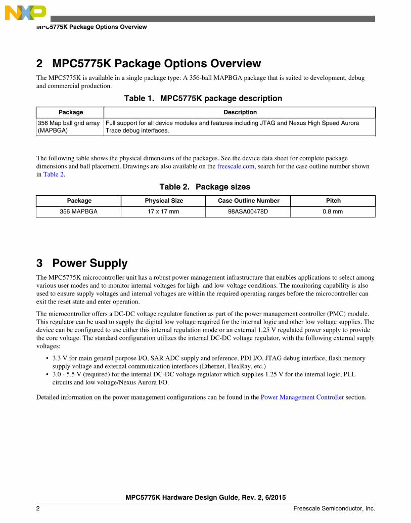
2 MPC5775K Package Options OverviewThe MPC5775K is available in a single package type: A 356-ball MAPBGA package that is suited to development, debugand commercial production.
Table 1. MPC5775K package description
Package Description
356 Map ball grid array(MAPBGA)
Full support for all device modules and features including JTAG and Nexus High Speed AuroraTrace debug interfaces.
The following table shows the physical dimensions of the packages. See the device data sheet for complete packagedimensions and ball placement. Drawings are also available on the freescale.com, search for the case outline number shownin Table 2.
Table 2. Package sizes
Package Physical Size Case Outline Number Pitch
356 MAPBGA 17 x 17 mm 98ASA00478D 0.8 mm
3 Power SupplyThe MPC5775K microcontroller unit has a robust power management infrastructure that enables applications to select amongvarious user modes and to monitor internal voltages for high- and low-voltage conditions. The monitoring capability is alsoused to ensure supply voltages and internal voltages are within the required operating ranges before the microcontroller canexit the reset state and enter operation.
The microcontroller offers a DC-DC voltage regulator function as part of the power management controller (PMC) module.This regulator can be used to supply the digital low voltage required for the internal logic and other low voltage supplies. Thedevice can be configured to use either this internal regulation mode or an external 1.25 V regulated power supply to providethe core voltage. The standard configuration utilizes the internal DC-DC voltage regulator, with the following external supplyvoltages:
• 3.3 V for main general purpose I/O, SAR ADC supply and reference, PDI I/O, JTAG debug interface, flash memorysupply voltage and external communication interfaces (Ethernet, FlexRay, etc.)
• 3.0 - 5.5 V (required) for the internal DC-DC voltage regulator which supplies 1.25 V for the internal logic, PLLcircuits and low voltage/Nexus Aurora I/O.
Detailed information on the power management configurations can be found in the Power Management Controller section.
MPC5775K Package Options Overview
MPC5775K Hardware Design Guide, Rev. 2, 6/2015
2 Freescale Semiconductor, Inc.

3.1 Power Supply Signals and DecouplingTable 3 lists all MCU power domains with corresponding pin names. Depending on the power management configuration,some of the supplies below may not require an external power source. The power management configuration is detailed inPower Management Controller.
Table 3. MCU power supply pins
Domain name SupplyVoltage
Description
VDD_LV_CORE 1.25 V Low-voltage supply for core logic
VDD_HV_IOx 3.3 V High-voltage supply for general purpose I/O
VDD_HV_RAW 3.3 V High-voltage, high fidelity supply for analog front-end block
VDD_HV_DAC 3.3 V High-voltage supply for DAC module in analog front-end
VDD_HV_ADC 3.3 V Voltage supply for SAR ADC module
VDD_HV_ADCREF0/2 3.3 V Voltage reference for SAR ADC 0/2
VDD_HV_ADCREF1/3 3.3 V Voltage reference for SAR ADC 1/3
VDD_HV_FLA 3.3 V Voltage supply for flash memory
VDD_HV_IO_PDI 3.3 V or 1.8 V PDI I/O voltage supply
VDD_HV_PMU 3.3 V Voltage supply for power management unit
VDD_HV_REG3V8 3.0 V - 5.5 V1 Voltage supply for internal DC-DC voltage regulator
VDD_LV_LFASTPLL2 1.25 V Voltage supply for DigiRF (SIPI/LFAST) PLL
VDD_LV_IO_AURORA3 1.25 V Voltage supply for Nexus Aurora I/O
VDD_LV_PLL0 1.25 V Voltage supply for system PLL
VDD_LV_IO 1.25 V Low voltage supply for general purpose I/O
1. Internal regulation mode. When using external regulation mode, this domain can be tied to VDD_HV_PMU2. The naming convention VDD_LV_LFASTPLL is equal to VDD_LV_DRFPLL3. VDD_LV_IO_AURORA must be connected to the same voltage supply as VDD_LV_CORE. The supplies must be brought
up simultaneously.
Some of the supplies can be powered with different supply voltages. The parallel digital interface (PDI) communicationsinterface can operate at 3.3 V or alternatively at 1.8 V for input only mode. The internal voltage regulator supply,VDD_HV_PMU, can be supplied with a voltage between 3.0 V and 5.5 V. See the device data sheet for specific informationand to learn what voltage ranges can be safely connected to the power pins.
Table 4 shows all power domains and the suggested decoupling and/or filter capacitors for their corresponding pins. Thesevalues are provided as a guideline and will vary depending on the application and capability of the power supplies used.
The decoupling capacitors must be placed as close as possible to the MCU supply pins, with priority given to those with thesmallest capacitance value..
Table 4. Supply pin decoupling capacitors
Domain name SupplyVoltage
Minimum Decoupling Capacitors
VDD _LV_CORE 1.25 V 0.1 μF x 16, 4.7 μF x 4, 10 μF x 2 (40 μF total)1
VDD_HV_IOx 3.3 V 2 x 0.1 μF for each VDD_HV_IO supply2
VDD_HV_RAW 3.3 V 0.1 μF, 1 μF
VDD_HV_DAC 3.3 V 1000 pF, 0.1 μF, 1 μF
Table continues on the next page...
Power Supply
MPC5775K Hardware Design Guide, Rev. 2, 6/2015
Freescale Semiconductor, Inc. 3
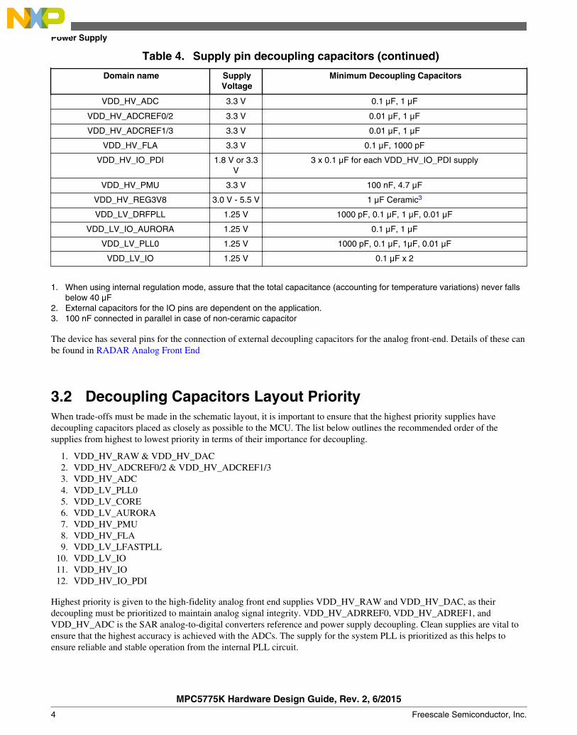
Table 4. Supply pin decoupling capacitors (continued)
Domain name SupplyVoltage
Minimum Decoupling Capacitors
VDD_HV_ADC 3.3 V 0.1 μF, 1 μF
VDD_HV_ADCREF0/2 3.3 V 0.01 μF, 1 μF
VDD_HV_ADCREF1/3 3.3 V 0.01 μF, 1 μF
VDD_HV_FLA 3.3 V 0.1 μF, 1000 pF
VDD_HV_IO_PDI 1.8 V or 3.3V
3 x 0.1 μF for each VDD_HV_IO_PDI supply
VDD_HV_PMU 3.3 V 100 nF, 4.7 μF
VDD_HV_REG3V8 3.0 V - 5.5 V 1 μF Ceramic3
VDD_LV_DRFPLL 1.25 V 1000 pF, 0.1 μF, 1 μF, 0.01 μF
VDD_LV_IO_AURORA 1.25 V 0.1 μF, 1 μF
VDD_LV_PLL0 1.25 V 1000 pF, 0.1 μF, 1μF, 0.01 μF
VDD_LV_IO 1.25 V 0.1 μF x 2
1. When using internal regulation mode, assure that the total capacitance (accounting for temperature variations) never fallsbelow 40 μF
2. External capacitors for the IO pins are dependent on the application.3. 100 nF connected in parallel in case of non-ceramic capacitor
The device has several pins for the connection of external decoupling capacitors for the analog front-end. Details of these canbe found in RADAR Analog Front End
3.2 Decoupling Capacitors Layout PriorityWhen trade-offs must be made in the schematic layout, it is important to ensure that the highest priority supplies havedecoupling capacitors placed as closely as possible to the MCU. The list below outlines the recommended order of thesupplies from highest to lowest priority in terms of their importance for decoupling.
1. VDD_HV_RAW & VDD_HV_DAC2. VDD_HV_ADCREF0/2 & VDD_HV_ADCREF1/33. VDD_HV_ADC4. VDD_LV_PLL05. VDD_LV_CORE6. VDD_LV_AURORA7. VDD_HV_PMU8. VDD_HV_FLA9. VDD_LV_LFASTPLL
10. VDD_LV_IO11. VDD_HV_IO12. VDD_HV_IO_PDI
Highest priority is given to the high-fidelity analog front end supplies VDD_HV_RAW and VDD_HV_DAC, as theirdecoupling must be prioritized to maintain analog signal integrity. VDD_HV_ADRREF0, VDD_HV_ADREF1, andVDD_HV_ADC is the SAR analog-to-digital converters reference and power supply decoupling. Clean supplies are vital toensure that the highest accuracy is achieved with the ADCs. The supply for the system PLL is prioritized as this helps toensure reliable and stable operation from the internal PLL circuit.
Power Supply
MPC5775K Hardware Design Guide, Rev. 2, 6/2015
4 Freescale Semiconductor, Inc.

Medium priority is given to VDD_LV_CORE, VDD_LV_DRFPLL, VDD_LV_AURORA, VDD_HV_PMU, andVDD_HV_FLA. VDD_LV_CORE is the main supply for the on-chip digital logic and this is prioritized as it affects thelargest amount of logic on the device. VDD_LV_AURORA powers the high speed Nexus Aurora pins and noise on thisdomain would affect the quality of the output. VDD_HV_PMU is the power management unit supply and VDD_HV_FLA isthe input supply for the flash memory. A good supply to the flash memory ensures reliable flash programming and erasing.
VDD_LV_DRFPLL powers the PLL for the LFAST/SIPI communication interface. VDD_HV_IO, VDD_LV_IO,VDD_IO_PDI drive GPIO and other external communication interfaces. Although it is still important that these supplieshave a clean power signal, the hardware they power is less affected by noise and they are considered of lower priority.
3.3 Power Management ControllerThe MPC5775K has a dedicated module for configuration and monitoring of power supplies, enable signals, internalcomponent trimming, and power-on reset generation. The Power Management Controller (PMC) consists of an analog blockand a supporting digital interface that provides control over the analog components. The Power Management Controllerchapter in the device reference manual explores the digital block in some depth.
NOTEThis document will focus on the external hardware and connections concerned with thePMC analog block.
3.3.1 Core Supply OptionsThe MPC5775K offers two options for supplying the 1.25 V used by the core and other low-voltage digital power domains.
• Internal voltage regulation mode, using the integrated DC-DC voltage regulator (VREG)• External voltage regulation mode using an externally regulated 1.25 V supply
The input pin VREG_SEL allows selection between internal and external regulation modes, the function of this input isdescribed in the table below.
Table 5. VREG_SEL input signal
Input Level Core Supply Mode
High (3.3V) Internal regulation mode
Low (GND) External regulation mode
The Power Management Controller (PMC) has an internal voltage regulator function that uses a switched-mode power supply(SMPS) circuit to supply the 1.25 V required by the internal core logic, (VDD_LV_CORE) and the other low-voltage digitalsupplies (VDD_LV_AURORA, VDD_LV_PLL0 and VDD_LV_IO). The regulator requires the support of external circuitrydetailed in SMPS External Component Configuration. This configuration is an asynchronous buck regulator with nominalswitching frequency of 1 MHz. The switching frequency is modulated to improve the EMI performance of the device, furtherinformation on this feature can be found in the PMC chapter in the device reference manual.
Power Supply
MPC5775K Hardware Design Guide, Rev. 2, 6/2015
Freescale Semiconductor, Inc. 5
VREG_SEL is part of a collection of I/O signals that relate to the VREG operation mode. The other pins are mentioned in thetable below.
Table 6. PMC Voltage regulator signals
Signal Name Direction VREG Enabled (Internal Mode) VREG Disabled (External Mode)
VREG_POR_B Input External power-on reset. If not required,can be left floating or connected to 3.3 V
supply. Pulled up internally to 3.3 V
Power-on reset(POR) input. Used byexternal circuitry to trigger a POR or hold
device in reset state
VREG_ISENS Input Current sense input to internal regulator Not used. Connect to VDD_LV_CORE
VREG_SWP Output Output from internal VREG. Controls thegate of the external switching PMOS
transistor 1
Not used, can be left floating
1. If the connection between VREG_SWP and the PMOS gate is broken, the switch may fully turn on. For added protectionagainst this risk, a 100 Kilo Ohm resistor can be connected between VDD_HV_REG3V8 and the PMOS gate.
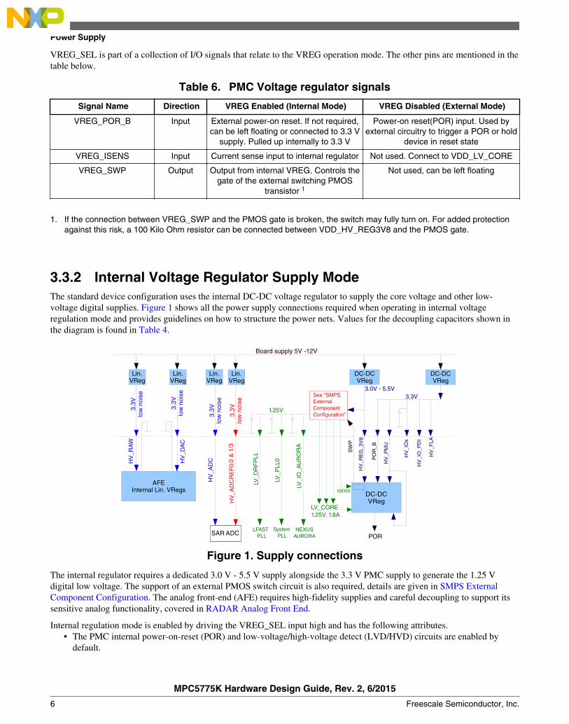
3.3.2 Internal Voltage Regulator Supply ModeThe standard device configuration uses the internal DC-DC voltage regulator to supply the core voltage and other low-voltage digital supplies. Figure 1 shows all the power supply connections required when operating in internal voltageregulation mode and provides guidelines on how to structure the power nets. Values for the decoupling capacitors shown inthe diagram is found in Table 4.
DC-DCVReg
Board supply 5V -12V
DC-DCVReg
SW
P
SAR ADC
3.3V
low
noi
se
POR
Lin.VReg
Lin.VReg
3.3V
low
noi
se
Lin.VReg
Lin.VReg
PO
R_B
DC-DCVReg
AFEInternal Lin. VRegs
3.3V
low
noi
se
3.3V
low
noi
se
HV
_PM
U
3.3V
HV
_RE
G_3
V8
3.0V - 5.5V
LV_D
RF
PLL
LV_P
LL0
LFAST PLL
System PLL
HV
_AD
CR
EF
0/2
& 1
/3
HV
_AD
C
1.25V
HV
_DA
C
HV
_RA
W
LV_I
O_A
UR
OR
A
NEXUSAURORA
See "SMPSExternalComponent Configuration"
HV
_FLA
HV
_IO
x
ISENS
LV_CORE1.25V, 1.8A
HV
_IO
_PD
I
Figure 1. Supply connections
The internal regulator requires a dedicated 3.0 V - 5.5 V supply alongside the 3.3 V PMC supply to generate the 1.25 Vdigital low voltage. The support of an external PMOS switch circuit is also required, details are given in SMPS ExternalComponent Configuration. The analog front-end (AFE) requires high-fidelity supplies and careful decoupling to support itssensitive analog functionality, covered in RADAR Analog Front End.
Internal regulation mode is enabled by driving the VREG_SEL input high and has the following attributes.• The PMC internal power-on-reset (POR) and low-voltage/high-voltage detect (LVD/HVD) circuits are enabled by
default.
Power Supply
MPC5775K Hardware Design Guide, Rev. 2, 6/2015
6 Freescale Semiconductor, Inc.
• The internal POR will keep the device in reset until all the monitored supplies have reached their minimum operationthreshold.
• The internal POR function means that the external POR pin VREG_POR_B is not needed. As such, it is internallypulled up to the PMC supply voltage. It can be left floating or alternatively connected to 3.3 V.
• VREG_POR_B remains active in internal regulation mode, even though POR is managed internally. If pulled low itwill cause a power-on reset regardless of voltage regulation mode.1
• The internal LVD/HVD circuits are enabled by default to ensure the expected boot-up sequence occurs. Moreinformation on the LVDs/HVDs is available in Low-Voltage (LVD) and High-Voltage Detection (HVD).
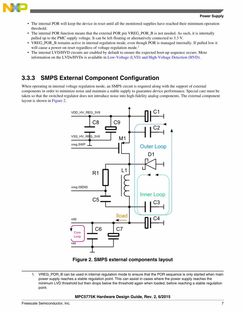
3.3.3 SMPS External Component ConfigurationWhen operating in internal voltage regulation mode, an SMPS circuit is required along with the support of externalcomponents in order to minimize noise and maintain a stable supply to guarantee device performance. Special care must betaken so that the switched regulator does not introduce noise into high-fidelity analog components. The external componentlayout is shown in Figure 2.
Figure 2. SMPS external components layout
1. VREG_POR_B can be used in internal regulation mode to ensure that the POR sequence is only started when mainpower supply reaches a stable regulation point. This can assist in cases where the power supply reaches theminimum LVD threshold but then drops below the threshold again when loaded, before reaching a stable regulationpoint.
Power Supply
MPC5775K Hardware Design Guide, Rev. 2, 6/2015
Freescale Semiconductor, Inc. 7

Table 7 provides recommended values for the external components.
Table 7. External component values
Component Label Recommended Value
M1 SI3443, 2SQ2315
L1 2.2 μH 3A <100 mΩ series resistance (E.g. Bourns SRU8043-2R2Y)
D1 SS8P3L 8A Schottcky diode
R1 240 kΩ
C1 10 μF ceramic
C2 100 nF ceramic
C3 100 nF ceramic (place close to inductor)
C4 10 μF ceramic (place close to inductor)
C5 100 pF ceramic
C6 4x 100 nF + 4x 10 nF ceramic (place close to MCU supply pins)
C7 4x 10 μF ceramic (place close to MCU supply pins)1
C8 100 nF ceramic (place close to MCU supply pins)
C9 1 μF ceramic (place close to MCU supply pins)
1. These are the same capacitors as those listed for VDD_LV_CORE in Table 2
For optimum electro-magnetic interference(EMI) performance, it is critical that the inner and outer loops shown in Figure 2overlap on the PCB and are made as short as possible. It is highly recommended to have a section of the PCB ground planededicated to making a good connection between the grounds of C1/C2 and C3/C4. This measure will help to ensure that theloops are made as short as possible.
The role of C1/C2 is to guarantee a low input impedance to the buck converter. In a similar manner, C3/C4 make theimpedance low at the buck converter output. This measure helps reduce the high frequency content of the current passingthrough the highlighted branch 'Iload', making it less critical that the buck converter components be placed close to theVDD/VSS pins of the MCU. However, it is important that capacitors C6 and C7 are placed as closely as possible to theVDD/VSS pins of the MCU, as they guarantee the low impedance of the core MCU supply and also help to reduce the highfrequency content of the 'Iload' path.
The gate-driver circuitry also forms important current loops that must be minimized (not shown in Figure 2). For thatpurpose, C8/C9 must be placed as close as possible to the gate-driver supply pins. The ground connections for C8/C9 must bemade as short as possible to C1/C2. When the PMOS switch is turned on, the high-frequency current that charges the gatecomes from C1/C2, passing through the PMOS gate into the gate-driver pin. That current is carried to the gate-driver VSS pinreturning to C1/C2. This current loop must be made as small as possible.
Conversely, when the PMOS switch is turned off, high-frequency currents enter in the PMOS gate coming from the gate-driver pin and flow into C1/C2, returning through the ground into C8/C9 and then into the gate-driver supply pin. Minimizingthis second loop area is as critical as the first.
To shield nearby nets from the gate-driver generated noise, it is also recommended that the gate-driver supply pins are usedto shield the VREG_SWP net until it reaches the PMOS switch. Nets on other PCB layer should avoid running parallel to thisnet.
The figure below is a circuit schematic showing an example SMPS circuit derived from the guidelines. For best performance,use the component values recommended in Table 7.
Power Supply
MPC5775K Hardware Design Guide, Rev. 2, 6/2015
8 Freescale Semiconductor, Inc.

VDD_LV_COREVDD_LV_*
VDD_HV_REG3V8
VDD_HV_REG3V8
Figure 3. Example schematic of SMPS external components
3.3.4 External Supply ModeIf there is a stable 1.25 V regulated supply available to provide the digital low voltage, the internal voltage regulator can bedisabled. This also negates the need for the external SMPS circuit. An overview of the power connections required for such aconfiguration is shown in Figure 4
DC-DCVReg
Board supply 5V -12V
SAR ADC
3.3V
low
noi
se
POR
Lin.VReg
Lin.VReg
3.3V
low
noi
se
Lin.VReg
Lin.VReg
PO
R_B
DC-DCVReg
AFEInternal Lin. VRegs
3.3V
low
noi
se
3.3V
low
noi
se
HV
_PM
U
3.3V
HV
_RE
G_3
V8
LV_D
RF
PLL
LV_P
LL0
LFAST PLL
System PLL
HV
_AD
CR
EF
0/2
& 1
/3
HV
_AD
C
1.25V
HV
_DA
C
HV
_RA
W
LV_I
O_A
UR
OR
A
NEXUSAURORA
DC-DCVReg
HV
_FLA
HV
_IO
x
LV_CORE1.25V, 1.8A
HV
_IO
_PD
I
Figure 4. Supply connections
This mode of operation can be selected by driving the VREG_SEL pin low. This disables the internal:
• Voltage regulator (VREG)
Power Supply
MPC5775K Hardware Design Guide, Rev. 2, 6/2015
Freescale Semiconductor, Inc. 9
• VDD_LV POR function (can be enabled by software)• VDD_LV LVD/HVD circuits (can be enabled by software)
When internal regulation is disabled, the signals VREG_ISENS and VREG_SWP are not needed as they are for feedback andcontrol of the SMPS circuitry. VREG_ISENS should be connected to VDD_LV_CORE and VREG_SWP connected toVDD_HV_PMU.
In external regulation mode, the supply for the internal voltage regulator, VDD_HV_REG3V8, can be connected to the samesupply voltage as VDD_HV_PMU.
VDD_LV POR and LVD/HVD is the responsibility of the external regulation circuit. The device must be kept in reset(VREG_POR_B driven low) during power-up until all supplies have reached their minimum operating threshold and alsoduring operation if any of the supplies move outside the specified range, as defined in the device data sheet. To achieve this,external LVD/HVD circuits are needed to monitor the supplies. After power-up, the internal LVDs/HVDs can be enabled bysoftware to act as a second tier of detection and provide power supply information to the software.
3.4 Supply MonitoringThe MPC5775K has the capability to monitor selected supply voltages internally. This section concerns only the internalmonitoring functions for POR and LVD/HVD, external POR and LVD/HVD circuit behavior will vary and should bedesigned using the device data sheet as reference. From this point, it is assumed that internal regulation mode is being usedunless where explicitly stated. In external regulation mode, the internal POR and LVD/HVD are disabled by default but canbe enabled by software after power-up.
The function of the power-on reset (POR) and low-voltage detect (LVD) circuits is to hold the device in reset as long as thesupply voltages to the LVD circuits are below the minimum operating voltage. The device is held in reset until the point atwhich the supplies cross the lower threshold and the POR and LVDs are released.
3.4.1 Behavior of LVD / HVDThe internal LVD and HVD circuits monitor when the voltage on the corresponding supply is below or above defined valuesand either assert a reset or an interrupt. The LVDs/HVDs also support hysteresis for the falling and rising trip points.
Although there is an option to disable the LVDs and HVDs following reset, they are capable of being used in a ‘monitor’only mode and also capable of generating a safe/interrupt event. The LVDs/HVDs can also be configured after deviceinitialization to prevent reset when a supply crosses the LVD threshold, providing a higher voltage range. An applicationmust then verify that the device remains in the functional range.
NOTEThe LVDs that form the power-on reset functionality, monitoring VDD_LV_CORE andVDD_HV_PMU, cannot be disabled. These modules are used during power-up phase andmust ensure that an absolute lowest threshold of operation is never crossed. This is not aguarantee that the device will function down to this level. It is rather a guarantee that thedevice will recover if this level is crossed.
3.4.2 Low-Voltage (LVD) and High-Voltage Detection (HVD)The internal LVD circuits monitor when the voltage on the corresponding supply is below defined values and either assert areset or an interrupt, while the HVD circuits monitor to ensure a supply does not exceed an upper voltage limit. The LVDs/HVDs also support hysteresis in the falling and rising trip points.
• All LVDs and HVDs are capable of generating either a reset or an interrupt based on configuration, with the exceptionof two POR threshold monitors2 :
Power Supply
MPC5775K Hardware Design Guide, Rev. 2, 6/2015
10 Freescale Semiconductor, Inc.
• LVD monitoring the internal core voltage (VDD_LV_CORE) always generates a reset when triggered.• LVD monitoring the PMC voltage supply input (VDD_HV_PMU) always generates a reset when triggered.
• All LVDs and HVDs configured for reset generation cause functional or destructive reset. Reset is not exited until alldestructive reset conditions are cleared.
• The appropriate bits in the PMC status registers are set by LVD and HVD events.• LVD and HVD control is protected by the SoC-wide register protection scheme. Therefore, it is configurable as long as
the scheme is followed.• There are user option bits available to allow degrading of “configurable” LVDs/HVDs from destructive down to
functional reset. This is a write once mechanism managed by SSCM during device initialization.• When the LVD or the HVD is enabled for destructive reset generation, then when a trigger event is detected, the
external RESET_B pin is driven low.
Please refer to the device data sheet for LVD and HVD characteristics.
3.4.3 Power-on ResetThe power management controller (PMC) controls the internal power-on reset (POR) signal for the MCU. POR is thecombination of all internal POR signals from the analog PMC block. When the critical power supplies are below minimumlevels(internal regulation mode) or the VREG_POR_B pin is driven low, the MCU is held in the POWERUP phase of thereset state machine, POR asserted, until the power supplies have reached their specified levels. When the required voltagelevels have been reached, POR is deasserted and is input to the reset generation module (MC_RGM) which propagates thedevice through the next steps of the boot process.
The PMC has internal POR low voltage detect(LVD) circuits to detect the minimum critical power supply voltages requiredto operate the internal voltage regulator, including hysteresis. It monitors:
• The voltage on the 1.25 V supply input, VDD_LV_CORE• The 3.3 V signal used internally by the PMC, VDD_HV_PMU
Once both these supply voltages are above the threshold the internal POR signal will deassert. See Device ResetConfiguration and the Reset chapter in the reference manual for VREG_POR_B and RESET_B pin functionality.
3.5 Power SequenceThe device is considered to be in a power sequence (POWER-UP state) when the device is either not supplied or is partiallysupplied. An internal power-on reset (POR) signal is used to identify POWER-UP state. This signal is released on exit of thepower sequence. The power-on reset signal is a combination of LVD monitoring of the VDD_LV_CORE andVDD_HV_PMU supplies. Exit from the next phase, PHASE0, depends on the release of the secondary LVD/HVD circuits,which monitor:
• VDD_LV_PLL0• VDD_HV_IO• VDD_HV_FLA• VDD_HV_ADC
Once they have reached the minimum operating threshold the device will exit reset. For more information on phases of thereset process, please refer to the Reset chapter in the device reference manual.
The actual threshold use for each internal LVD depends on the configuration of the device. This is configurable by hardware(flash option bits content) or by software (LVD event configuration through PMC register interface). Once the power-onsignal has been asserted, the device configuration is reset to default power-up configuration. During the initialization phase,
2. As mentioned previously, the internal POR management is disabled by default when external regulation mode isselected. They cannot be disabled when operating in internal VREG mode.
Power Supply
MPC5775K Hardware Design Guide, Rev. 2, 6/2015
Freescale Semiconductor, Inc. 11

the device defaults to a pre-determined state for each of the LVDs, HVDs, and the internal regulators. As the flash memorybecomes available, the differential read process allows the trimmed data to be available for trimming the internal LVDs,HVDs, and regulators.
3.5.1 Power-up SequenceIn this section, the assumption is made that all supplies are low when entering the power-up sequence. Brown-out and powerdown sequences are specified in following sections.
There are simple power sequencing rules to follow in order to correctly power-up the device:• The system PLL supply (VDD_LV_PLL0) and the core supply (VDD_LV_CORE) must be powered simultaneously. It
is recommended to connect them to the same voltage supply.• The high-voltage I/O supply (VDD_HV_IO) and the Power Management Unit supply (VDD_HV_PMU) must be
powered simultaneously or VDD_HV_IO ramped before VDD_HV_PMU such that the two supplies always maintainless than 100 mV difference during the power ramp. They can be connected to the same voltage supply.
• The SD ADCs must be powered before a signal is applied to their inputs, to ensure protection of the input channelsfrom overdrive signal levels. To do this, ramp VDD_HV_RAW supply before applying input to the SD ADCs.
All power supplies should ramp at slew rates within the ranges recommended in the device data sheet.
3.5.2 Power-down SequenceIf the threshold of the configurable monitor LVDs is crossed and they are configured to generate a destructive reset, thedevice re-enters the PHASE0 phase. The power-down sequence is started and the device enters the POWER-UP state as soonas the threshold of one of the POR LVDs (monitoring VDD_LV_CORE and VDD_HV_PMU) is crossed. The devicesupplies may then proceed to drop down to ground either through device leakage or external pull-down.
3.5.3 Brown-out ManagementDuring brown-out, the device re-enters the POWER-UP phase as soon as the threshold of either POR VDD 1.2 V or APOR iscrossed.
4 Clock ConfigurationThe MPC5775K system reference clock can be sourced in two ways: using the internal RC oscillator (IRCOSC) orconnecting an external oscillator (XOSC). To use XOSC, an external 40 MHz crystal or oscillator must be connected throughthe XTAL and EXTAL pins. Information on how to do this can be found in Connecting External Clock Sources. IRCOSC orXOSC is used as the clock source for the internal phase-locked loops (PLL) to generate the high frequency clocks for thecores and peripherals.
This structure provides five different clock domains that are available as the source for system and peripheral clocks:• IRCOSC - 16 MHz internal reliable RC oscillator• XOSC - 40 MHz oscillator (using external crystal (XTAL) or external oscillator in bypass (EXTAL))• PLL0 - up to 266 MHz PLL• PLL1 - up to 266 MHz frequency-modulated (FM) PLL• SDPLL- 320 MHz3 PLL for the Sigma-Delta ADC
3. Divided by 2 (160 MHz) if used for system and peripheral clocks
Clock Configuration
MPC5775K Hardware Design Guide, Rev. 2, 6/2015
12 Freescale Semiconductor, Inc.

XOSC 40MHz1-2ps JitterBypass:40MHz
FMPLL_1VCO:600-1250MHz
IRCOSC16MHz
Cryst40MHz
SDPLL320MHz
IRC_CLK
PLL_CLK0
PLL_CLK1
PLL_0VCO: 600-1250MHz
OSC40MHz
XOSC_CLK
SDPLL_CLK
AFEXTAL
EXTAL
Figure 5. MPC5775K clock sources
During power up, the IRCOSC is the default clock for the system. In normal operation, software can then configure each ofthe system components to use one of the clock domains as the clock source. The dual PLL must be enabled by software andcan provide separate system and peripheral clocks. PLL0 is the primary PLL driven by the reference clock and used toprovide a clock to the device modules. PLL1 is a frequency-modulated PLL (FMPLL) driven by PLL0 and is used to providethe system clock. Alternatively, XOSC can be used to drive PLL1.
The most important aspects of an accurate clock source require that some care be taken in the layout and design of thecircuitry around the crystal and PLL power supplies. Any noise in these circuits can affect the accuracy of the clock source tothe PLL. The power supply for the PLL is taken from VDD_LV_PLL0. Noise on this supply can affect the accuracy andjitter performance of the PLLs. In order to minimize any potential noise, it is recommended that the additional capacitorsrecommended in Table 4 are fitted to the VDD_LV_PLL0 supply.
4.1 Connecting External Clock SourcesThe MPC5775K features internal load capacitance on the XTAL and EXTAL pins for connecting external clock sources.This feature is intended to simplify the design and reduce the overall system cost by eliminating external components andreducing the PCB footprint. See the device data sheet for details on the internal capacitance values. PCB designers must takeinto account the parasitic capacitance levels on the signal lines connecting an external oscillator to the XTAL and EXTALpins in order to avoid frequency deviation. Generally, for a crystal with load capacitance of 8 pF, a capacitance figure of 5-6pF on the signal lines connected to both XTAL and EXTAL will result in good oscillator performance.
A diagram for the connection of an external 40 MHz crystal oscillator is shown in the figure below.
Clock Configuration
MPC5775K Hardware Design Guide, Rev. 2, 6/2015
Freescale Semiconductor, Inc. 13

XTAL EXTAL
Crystal
MPC5775K
Figure 6. External oscillator connection
The oscillator should be placed as close as possible to the MCU. In order to minimize signal degradation, the circuitry shouldbe placed entirely on only one PCB layer, avoiding unnecessary vias where possible. Do not allow any signals to cross thecrystal connections to the device. Absolutely no high current or high speed signals should be run near any of the crystalcomponents.
Other than the connections shown in the above schematics, no other connections should be made to the crystal or EXTALand XTAL device pins. Do not use XTAL to drive any other circuitry than shown.
If an external clock is being used as clock reference to the MCU, then the XTAL pin should be left floating and the clockshould be provided to EXTAL as shown in the figure below.
XTAL EXTAL
MPC5775K
40MHzClock
Figure 7. External clock connection (Bypass Mode)
Using either of these methods to connect an external clock makes it available as the XOSC internal clock source.
5 Device Reset ConfigurationThe MPC5775K MCU requires only very basic external reset circuitry. External circuitry for device configuration is notrequired. The device is configured during reset based on data in stored flash memory.
5.1 External Reset SignalsThe MPC5775K device features two active-low external reset signals:
• Functional reset (RESET_B)• Power-on reset (VREG_POR_B)
Device Reset Configuration
MPC5775K Hardware Design Guide, Rev. 2, 6/2015
14 Freescale Semiconductor, Inc.
RESET_B is a bidirectional reset input/output that indicates if the device is active (high signal) or in reset. It is thus weakpull-up after the reset sequence has completed. A falling edge on this pin will trigger a functional reset to the ResetGeneration Module(RGM). Forcing this pin low will keep the device in the last phase of the reset sequence(Phase3[Functional]).
In external voltage regulation mode, VREG_POR_B allows external supply circuits to signal to the MCU when power isavailable so the power-up sequence can begin. It should be forced high when the critical power supplies cross the LVDthreshold.
In internal regulation mode, VREG_POR_B is not needed as the POR is managed within the PMC. It is internally pulled upto the PMC voltage, so it can be left floating. Alternatively, it can be connected to VDD_HV_PMU through a 4.7 Kilo Ohmpull-up resistor. Note that VREG_POR_B remains active in internal regulation mode. As such, if it is pulled low it will causea power-on reset in the device.
Both of these pins operate on the 3.3 V power domain.
6 Recommended Debug Connectors And Connector Pin-outDefinitions
The MPC5775K microcontroller implements the newly added (in the IEEE-ISTO 5001™-2011 version of the standard) highspeed serial Nexus trace Auxiliary Port that uses the Xilinx™ Aurora physical interface. The Aurora interface allows theNexus protocol information to be transmitted serially at a high date rate over one or more Aurora lanes. The Aurora protocolhandles the encoding of the data and stripes the information across the number of lanes available on the device.
Table 8 shows the recommended connectors for different applications for the MPC57xxx Family.
Table 8. Recommended connectors
Connector style Target system part number Connector type
14-pin BERG JTAG only 3M 2514-6002UB JTAG-only configuration
17-position (2 × 17, 34-pin) Samtec Samtec ASP-137973-01 Serial Nexus configuration (supports upto 8 simplex lanes, less lanes areavailable if duplex support or HighSpeed Calibration LFAST interface
support is required)
NOTEWhichever connector is chosen, "keep-out" areas may be required by some tools. Consultthe preferred tool vendor to determine any area that must remain clear around the debugconnector. Some tool vendors may include an extension cable to minimize "keep-out"areas, but use of an extension will degrade the signal. In many cases, this degradation willbe insignificant, but it depends on many factors including clock frequency and targetboard layout.
6.1 MPC5775K JTAG ConnectorTable 9 shows the pinout of the recommended JTAG connector to support the MPC5775K device.
Recommended Debug Connectors And Connector Pin-out Definitions
MPC5775K Hardware Design Guide, Rev. 2, 6/2015
Freescale Semiconductor, Inc. 15

The recommended connector for the target system is Tyco part number 2514-6002UB.
Table 9. Recommended JTAG connector pinout
Description Pin Pin Description
TDI 1 2 GND/VSS
TDO 3 4 GND/VSS
TCK 51 6 GND/VSS
EVTI0 7 8 VREG_POR_B
RESET_B 9 10 TMS
VREF/VDD 11 12 GND/VSS
EVTO0 13 14 JCOMP
1. If LBIST is enabled, an external pull resistor between 1 Kilo and 100 Kilo Ohm must be connected between TCK and eitherVDD/VSS to avoid LBIST failures
Figure 8. Diagram of the JTAG connector pinout
6.2 MPC5775K High-Speed Nexus Serial Trace ConnectorFor high speed Nexus Aurora trace applications, the Samtec™ ERF8 Series connector is recommended in the IEEE-ISTO5001™-2011 standard. For the MPC57xx family, the 17 position (34 pins) connector is recommended. The part number ofthe Samtec connectors are shown in Table 10.
Table 10. Recommended high-speed serial trace connector part numbers
Connector Part number (Samtec) Style Description
HS34 ASP-137973-01 Samtec ERF8 Series, 17position by 2 row
Vertical mount for MCUmodule
HS34 ASP-177706-02 Samtec ERF8 Series, 17position by 2 row
Right Angle mount for MCUmodule
The Samtec ERF8 series of connectors is intended for high speed applications requiring a minimum footprint size with areliable, latching connection. The recommended connector has two rows of seventeen contacts each with a spacing of 0.8mm. The connector provides isolation between the high-speed trace signals and the low-speed JTAG and control signals. Italso provides ample ground connections to ensure signal integrity. If at all possible, the connector should be placed onto thetarget system with the even numbered pins nearest the edge of the printed circuit board.
Recommended Debug Connectors And Connector Pin-out Definitions
MPC5775K Hardware Design Guide, Rev. 2, 6/2015
16 Freescale Semiconductor, Inc.
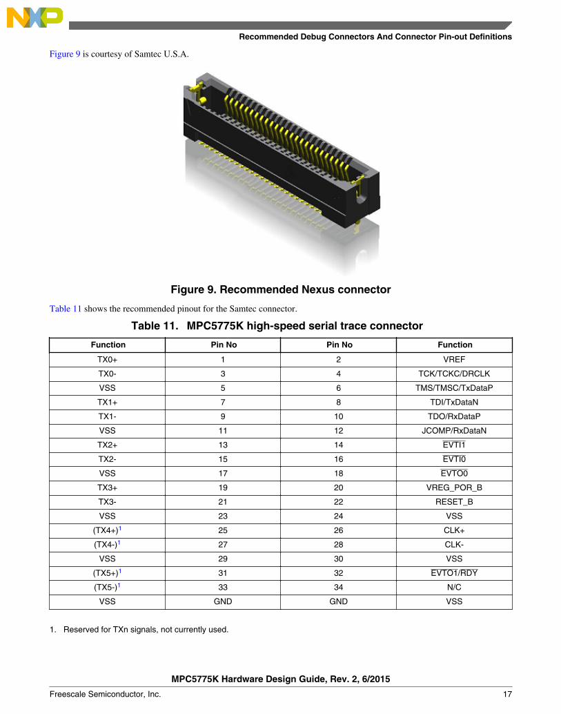
Figure 9 is courtesy of Samtec U.S.A.
Figure 9. Recommended Nexus connector
Table 11 shows the recommended pinout for the Samtec connector.
Table 11. MPC5775K high-speed serial trace connector
Function Pin No Pin No Function
TX0+ 1 2 VREF
TX0- 3 4 TCK/TCKC/DRCLK
VSS 5 6 TMS/TMSC/TxDataP
TX1+ 7 8 TDI/TxDataN
TX1- 9 10 TDO/RxDataP
VSS 11 12 JCOMP/RxDataN
TX2+ 13 14 EVTI1
TX2- 15 16 EVTI0
VSS 17 18 EVTO0
TX3+ 19 20 VREG_POR_B
TX3- 21 22 RESET_B
VSS 23 24 VSS
(TX4+)1 25 26 CLK+
(TX4-)1 27 28 CLK-
VSS 29 30 VSS
(TX5+)1 31 32 EVTO1/RDY
(TX5-)1 33 34 N/C
VSS GND GND VSS
1. Reserved for TXn signals, not currently used.
Recommended Debug Connectors And Connector Pin-out Definitions
MPC5775K Hardware Design Guide, Rev. 2, 6/2015
Freescale Semiconductor, Inc. 17
It is recommended that the "even" side of the connector be mounted closer to the edge of the printed circuit board to facilitatea direct connection to the tool.
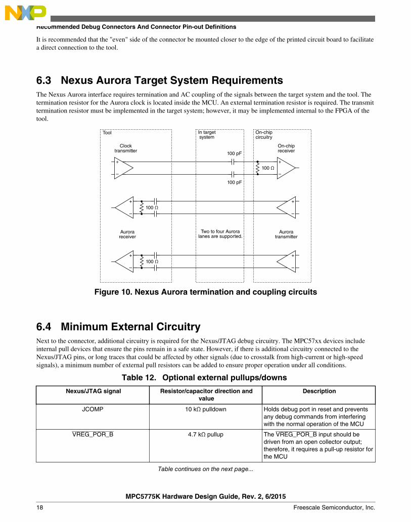
6.3 Nexus Aurora Target System RequirementsThe Nexus Aurora interface requires termination and AC coupling of the signals between the target system and the tool. Thetermination resistor for the Aurora clock is located inside the MCU. An external termination resistor is required. The transmittermination resistor must be implemented in the target system; however, it may be implemented internal to the FPGA of thetool.
+
–
+
–
Clock transmitter
100 Ω
On-chip receiver
In target system
+
–
+
–
Tool
+
–
+
–
Aurorareceiver
Auroratransmitter
Two to four Aurora lanes are supported.
On-chip circuitry
100 pF
100 pF
100 Ω
100 Ω
Figure 10. Nexus Aurora termination and coupling circuits
6.4 Minimum External CircuitryNext to the connector, additional circuitry is required for the Nexus/JTAG debug circuitry. The MPC57xx devices includeinternal pull devices that ensure the pins remain in a safe state. However, if there is additional circuitry connected to theNexus/JTAG pins, or long traces that could be affected by other signals (due to crosstalk from high-current or high-speedsignals), a minimum number of external pull resistors can be added to ensure proper operation under all conditions.
Table 12. Optional external pullups/downs
Nexus/JTAG signal Resistor/capacitor direction andvalue
Description
JCOMP 10 kΩ pulldown Holds debug port in reset and preventsany debug commands from interferingwith the normal operation of the MCU
VREG_POR_B 4.7 kΩ pullup The VREG_POR_B input should bedriven from an open collector output;therefore, it requires a pull-up resistor forthe MCU
Table continues on the next page...
Recommended Debug Connectors And Connector Pin-out Definitions
MPC5775K Hardware Design Guide, Rev. 2, 6/2015
18 Freescale Semiconductor, Inc.

Table 12. Optional external pullups/downs (continued)
Nexus/JTAG signal Resistor/capacitor direction andvalue
Description
RESET_B 4.7 kΩ pullup The RESET_B input should be drivenfrom an open collector output; therefore,it requires a pull-up resistor for the MCU
Nexus CLKP & CLKN 100 pF on the signal lines The LVDS Nexus clock signals require acapacitor for high speed functionality
EVTI 10 kΩ pullup A pullup resistor prevents debug modefrom being forced after reset if debugmode is enabled (JCOMP = high). It alsoprevents breakpoints from being forced ifdebug mode is enabled.
NOTE: In almost all situations, aresistor is not required on thissignal.
In addition to the pullup and pulldown resistors, some systems may want to use buffers between the JTAG connector inputs(JCOMP, TDI, TDO, TMS, EVTI, EVTO, VREG_POR_B, and RESET_B) and the MCU. This will prevent over-voltageconditions from causing damage to the MCU signals. Normal systems should not require this circuitry, but it is helpful insystems that can be exposed to improper connections that provide voltages that are outside the operating conditions of theMCU. A common circuit to use is the Texas Instruments™ SN74CBTLV38615. This device is a bus switch that implementsa bidirectional interface between two terminals with less than 5 Ω of resistance. It should be powered by the same supply thatpowers the debug port. The device enable should be connected to ground for the interface to be enabled whenever the debugport on the MCU is powered. This circuit provides a high impedance to the tool when the debug port is powered off.
7 ADC OverviewThe MPC5775K has two types of analog-to-digital converters (ADCs) that are designed for different applications:
• Four 12-bit Successive-Approximation-Register (SAR) ADCs with a configurable number of channels (up to 16 each)for voltage and temperature monitoring among other general applications
• Eight 12-bit Sigma-Delta (SD) ADC instances for rapid RADAR signal conversions
The SDADC is part of the RADAR analog front-end and is detailed in Sigma-Delta ADC. This chapter will focus on theSAR ADCs.
The SAR ADCs receive input from 25 multiplexed pins. Please refer to the Power Supply section for information on how toconnect the ADC power and reference pins.
Each ADC instance receives input from a number of pins(channels), some of which are multiplexed to share with other ADCinstances. This multiplexing, along with many other attributes of the ADCs, is controlled by configuration registers. EachADC instance has an interface to the DMA controller for retrieval of converted data, the FCCU for error handling and theinterrupt controller. Conversions can be triggered by hardware, software or externally:
• A Cross triggering unit (CTU) connected to each ADC allows automatic generation of ADC conversion requests onuser selected conditions without CPU involvement.
• eTimer module provides the capability for external trigger injection to request a conversion.• The CPU can request a conversion through software
ADC Overview
MPC5775K Hardware Design Guide, Rev. 2, 6/2015
Freescale Semiconductor, Inc. 19

7.1 SAR Analog Input Pin MultiplexingThere are 25 external analog pins that act as input channels for the SAR ADCs. They are multiplexed in order to facilitatesharing of the pins among the ADC instances.
There is an analog bypass bit "APC" in the Multiplexed Signal Configuration Register (MCSR) registers of the SystemIntegration Unit (SIUL2) for the pins to disable the digital circuitry from the analog pins.
Table 13 gives the analog input pin assignment for the MPC5775K 356MBGA package.
Table 13. ADC pin muxing
ADC Internal/External
Signal source PackageAvailabilityADC
InstanceChannel
NoSource External Pin
Shared external channels - ADC0/1
ADC0 11 External ADC0_AN[11]_ADC1_AN[11] PAD[25] All
ADC1 11
ADC0 12 External ADC0_AN[12]_ADC1_AN[12] PAD[26] All
ADC1 12
ADC0 13 External ADC0_AN[13]_ADC1_AN[13] PAD[27] All
ADC1 13
ADC0 14 External ADC0_AN[14]_ADC1_AN[14] PAD[28] All
ADC1 14
ADC0 external channels
ADC0 0 External ADC0_AN[0] PAD[23] All
ADC0 1 External ADC0_AN[1] PAD[24] All
ADC0 2 External ADC0_AN[2] PAD[33] All
ADC0 3 External ADC0_AN[3] PAD[34] All
ADC0 4 External ADC0_AN[4] PAD[70] All
ADC0 5 External ADC0_AN[5] PAD[66] All
ADC0 6 External ADC0_AN[6] PAD[71] All
ADC0 7 External ADC0_AN[7] PAD[68] All
ADC0 8 External ADC0_AN[8] PAD[69] All
ADC0 9 — not assigned — —
ADC0 10 Internal Bandgap Reference PMC — —
ADC0 15 Internal TSENS0 — —
ADC1 Channels
ADC1 0 External ADC1_AN[0] PAD[29] All
ADC1 1 External ADC1_AN[1] PAD[30] All
ADC1 2 External ADC1_AN[2] PAD[31] All
ADC1 3 External ADC1_AN[3] PAD[32] All
ADC1 9 — not assigned — —
ADC1 10 Internal Bandgap Reference PMC — —
ADC1 15 Internal TSENS1 — —
Shared external channels - ADC1/3
Table continues on the next page...
ADC Overview
MPC5775K Hardware Design Guide, Rev. 2, 6/2015
20 Freescale Semiconductor, Inc.

Table 13. ADC pin muxing (continued)
ADC Internal/External
Signal source PackageAvailabilityADC
InstanceChannel
NoSource External Pin
ADC1 4 External ADC1_AN[4]_ADC3_AN[3] PAD[75] All
ADC3 3
ADC1 5 External ADC1_AN[5]_ADC3_AN[4] PAD[64] All
ADC3 4
ADC1 6 External ADC1_AN[6]_ADC3_AN[5] PAD[76] All
ADC3 5
ADC1 7 External ADC1_AN[7]_ADC3_AN[6] PAD[73] All
ADC3 6
ADC1 8 External ADC1_AN[8]_ADC3_AN[7] PAD[74] All
ADC3 7
Shared external channels - ADC2/3
ADC2 0 External ADC2_AN[0]_ADC3_AN[0] PAD[149] All
ADC3 0
ADC2 1 External ADC2_AN[1]_ADC3_AN[1] PAD[150] All
ADC3 1
ADC2 2 External ADC2_AN2[]_ADC3_AN[2] PAD[151] All
ADC3 2
ADC2 channels
ADC2 5 Internal Reserved for factory test only--SWG (for testonly)
— —
ADC2 10 Internal Bandgap reference PMC — —
ADC3 channels
ADC3 10 Internal Bandgap Reference PMC — —
ADC3 11 Internal Reserved for factory test only--Reserved for ATX — —
ADC3 12 Internal Reserved for factory test only--Reserved for ATX — —
ADC3 13 Internal Reserved for factory test only--Reserved for ATX — —
ADC3 14 Internal Reserved for factory test only--Reserved for ATX — —
ADC0 and ADC1 Presampling
ADC0 PRESx Internal VREFP_ADC0 — —
ADC0 PRESx Internal VREFN_ADC0 — —
ADC1 PRESx Internal VREFP_ADC1 — —
ADC1 PRESx Internal VREFN_ADC1 — —
ADC2 and ADC3 Presampling
ADC2 PRESx Internal VREFP_ADC2 — —
ADC2 PRESx Internal VREFN_ADC2 — —
ADC3 PRESx Internal VREFP_ADC3 — —
ADC3 PRESx Internal VREFN_ADC3 — —
ADC Overview
MPC5775K Hardware Design Guide, Rev. 2, 6/2015
Freescale Semiconductor, Inc. 21
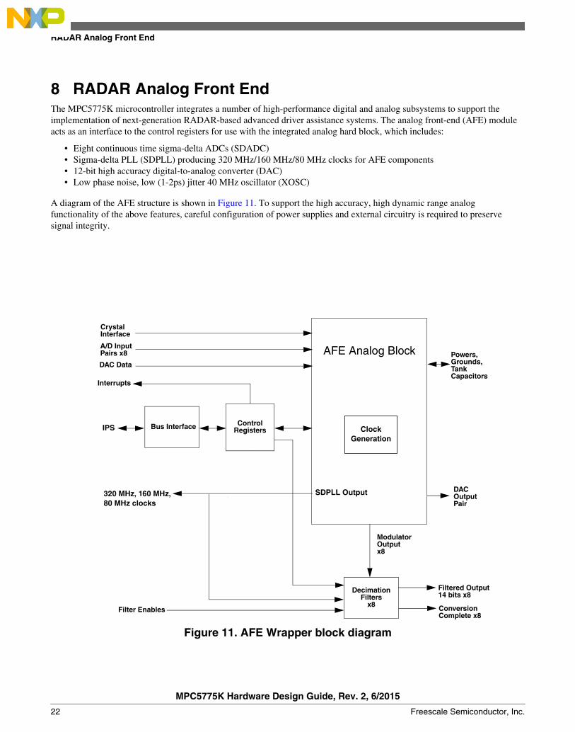
8 RADAR Analog Front EndThe MPC5775K microcontroller integrates a number of high-performance digital and analog subsystems to support theimplementation of next-generation RADAR-based advanced driver assistance systems. The analog front-end (AFE) moduleacts as an interface to the control registers for use with the integrated analog hard block, which includes:
• Eight continuous time sigma-delta ADCs (SDADC)• Sigma-delta PLL (SDPLL) producing 320 MHz/160 MHz/80 MHz clocks for AFE components• 12-bit high accuracy digital-to-analog converter (DAC)• Low phase noise, low (1-2ps) jitter 40 MHz oscillator (XOSC)
A diagram of the AFE structure is shown in Figure 11. To support the high accuracy, high dynamic range analogfunctionality of the above features, careful configuration of power supplies and external circuitry is required to preservesignal integrity.
Filtered Output
Bus Interface
DecimationFilters
x8
ModulatorOutputx8
14 bits x8
ConversionComplete x8
ControlRegisters
Interrupts
A/D InputPairs x8
CrystalInterface
DACOutputPair
Powers,Grounds,TankCapacitors
Filter Enables
DAC Data
ClockGeneration
AFE Analog Block
SDPLL Output320 MHz, 160 MHz,80 MHz clocks
IPS
Figure 11. AFE Wrapper block diagram
RADAR Analog Front End
MPC5775K Hardware Design Guide, Rev. 2, 6/2015
22 Freescale Semiconductor, Inc.
8.1 AFE Power Supplies and External ConnectionsThe AFE module requires multiple external connections. These are a mixture of high-fidelity analog power supplies, digitalpower supplies, ground connections, external capacitor connections and output signals for the various functions.
Table 14. AFE power supply connections
Name VoltageRange
Domain Function
VDD_HV_RAW 3.0 V - 3.6 V 3.3 V Connects to 1.4 V regulators for: XOSC, SD PLL and SDADC analog and digital.
VDD_HV_DAC 3.0 V - 3.6 V 3.3 V Connects to DAC regulator
The table below shows the pins that the AFE exposes for the connection of external components. The components should beconnected between the pin and ground.
Table 15. AFE external component connections
Pin Name Function Recommended
SD_R External 0.1% trimming resistor fortuning the ADC resistor array.
40.2 Kilo Ohm +/-0.1%
VDD_LV_SDCLK External bypass capacitor for LVDSanalog 1.4 V VREG.
1.0 μF & 0.1 μF grounded toVSS_LV_SDCLK
VDD_LV_OSC External bypass capacitor for XOSCanalog 1.4 V VREG
1.0 μF & 0.1 μF grounded toVSS_LV_OSC
VDD_LV_SDPLL External bypass capacitor for SD PLLanalog 1.4 V VREG.
1.0 μF & 0.1 μF grounded toVSS_LV_SDPLL
VDD_LV_RADARREF External bypass capacitor for 1.2 V fromthe VREF.
1.0 μF grounded to VSS_LV_SDADC
DAC_C DAC connection to external cap fornoise filtering.
10 μF connected to VDD_HV_DAC
SD_CM ADC common mode external bypasscapacitor
1.0 μF & 0.1 μF grounded toVSS_LV_SDADC
VDD_LV_SDADC External bypass capacitor for ADCanalog 1.4 V Vreg.
0.47 μF & 0.1 μF grounded toVSS_LV_SDADC
VDD_LV_RADARDIG External bypass capacitor for ADCdigital 1.4 V Vreg.
1.0 μF & 0.1 μF grounded toVSS_LV_RADARDIG
AFE_FILTER Bypass capacitor for filtered analogsupply
1.0 μF & 0.1 μF grounded toVSS_LV_SDADC
VDD_LV_DAC2V5 Bypass capacitor rampDAC 2.5 V VREG 1.0 μF & 0.1 μF grounded toVSS_HV_REGDAC
8.2 Sigma-Delta ADCThe eight time-continuous SD ADCs receive input as a differential pair. Each instance has two dedicated input pins.
RADAR Analog Front End
MPC5775K Hardware Design Guide, Rev. 2, 6/2015
Freescale Semiconductor, Inc. 23

Table 16. Sigma-Delta ADC external connections
Name Pin(356MBGA)
Direction Function
SD_0_ADCN A2 I ADC0 negative input
SD_1_ADCN A3 I ADC1 negative input
SD_2_ADCN A4 I ADC2 negative input
SD_3_ADCN A5 I ADC3 negative input
SD_4_ADCN A6 I ADC4 negative input
SD_5_ADCN A7 I ADC5 negative input
SD_6_ADCN A8 I ADC6 negative input
SD_7_ADCN A9 I ADC7 negative input
SD_0_ADCP B2 I ADC0 positive input
SD_1_ADCP B3 I ADC1 positive input
SD_2_ADCP B4 I ADC2 positive input
SD_3_ADCP B5 I ADC3 positive input
SD_4_ADCP B6 I ADC4 positive input
SD_5_ADCP B7 I ADC5 positive input
SD_6_ADCP B8 I ADC6 positive input
SD_7_ADCP B9 I ADC7 positive input
8.3 Digital-to-Analog ConverterThe DAC is used to produce analog ramp signals for generation of RADAR waveforms.
Table 17. DAC signal description
Name Pin (356MBGA) Direction Function
DAC_AN D8 O DAC negative output (current)Connected to external 300
Ohm resistor
DAC_AP C8 O DAC positive output (current)Connected to external 300
Ohm resistor
The resistors are required because the DAC output is a current source. Figure 12 shows how to connect the external resistorsto the DAC output pins.
RADAR Analog Front End
MPC5775K Hardware Design Guide, Rev. 2, 6/2015
24 Freescale Semiconductor, Inc.

MPC5775K
DAC_AP
DAC_AN
300 Ohm
300 Ohm
Figure 12. DAC Output Pin Connections
8.4 Sigma-Delta PLLThere are no external connections required for the Sigma-Delta PLL. Information on configuration can be found in theAnalog Front End chapter in the device reference manual.
8.5 XOSCInstructions on how to connect an external source to drive the XOSC clock can be found in Connecting External ClockSources.
Table 18. XOSC external connections
Name Pin (356MBGA) Direction Function
XOSC_EXTAL E1 I EXTAL analog input signal
XOSC_XTAL D1 O XTAL analog output signal
9 Example Communication Peripheral ConnectionsThere are a wide range of peripheral pins available on the MCU. Many of these have fairly standard definitions for their use.This section provides example connections for some of the most commonly used communications peripherals, such as LIN,FlexCAN, FlexRay, and RS-232 communication interfaces.
Example Communication Peripheral Connections
MPC5775K Hardware Design Guide, Rev. 2, 6/2015
Freescale Semiconductor, Inc. 25

9.1 Example RS232 InterfaceThe RS-232 (TIA/EIA-232-F) standard is a fairly common interface that is available on all computers. While this interface isdisappearing, adapters are available to allow the use of RS-232 peripherals through other interfaces, such as USB. RS-232was intended to be a very low-cost and low-performance interface. This interface was originally specified with signalvoltages of +12 V and –12 V, typically. However, this has been lowered to a typical minimum voltage of +5 V and –5 V inrecent years.
Figure 13 and Table 19 show the typical connections between the serial port of an MCU and the MAX3232-EP RS-232Dtransceiver from Texas Instruments http://www.ti.com/. The transceiver operates from either a 3.3 V or a 5 V supply andincludes two charge pumps to generate the output voltages that are required. This device contains two transmit drivers andtwo receivers. The charge pumps require four external capacitors.
+ 0.47uF +
0.1uF
3.3V or 5V
162738495
DB9F
FB
1
V+
C1-
C2+
C2-
V-
DOUT2
8
Vcc
16
GN
D 15
DOUT1
RIN1 ROUT1
DIN1
DIN2
ROUT2
0.1uF
SCI_TXDA
SCI_RXDA
MAX3232
SCI_RXDA2
HOST-R2 SCI_TXDA2
HOST-T2 9
HOST-R1
HOST-T1
+
0.47uF
+
0.47uF+
10
11
12
7
RIN2
14
13
2
4C1+
3
6
5
Figure 13. Typical SCI to RS232 circuit
NOTEThe commercial grade MAX3232 device is not rated for the full automotive temperatureof -40 to +125° C and is not intended for automotive applications. This circuit should notbe used or populated in a production module intended for automotive use. However, inmany cases, the RS-232 interface is intended only as a development interface; therefore,the commercial device can be used for prototyping purposes. Texas Instruments doesoffer a device option with an operating temperature range of -40 to +85° C. TexasInstruments has an enhanced version of the device, MAX3232-EP, that is intended foraerospace, medical, and defense applications. This version is available with an operatingtemperature range of –55 to +125° C.
Table 19. Typical RS-232D connector definition
Pin number Description
1 Connect to pin 4 and 6
2 RS-232 TX (Transmit)
3 RS-232 RX (Receive)
4 Connect to pin 1 and 6
5 GND
Table continues on the next page...
Example Communication Peripheral Connections
MPC5775K Hardware Design Guide, Rev. 2, 6/2015
26 Freescale Semiconductor, Inc.
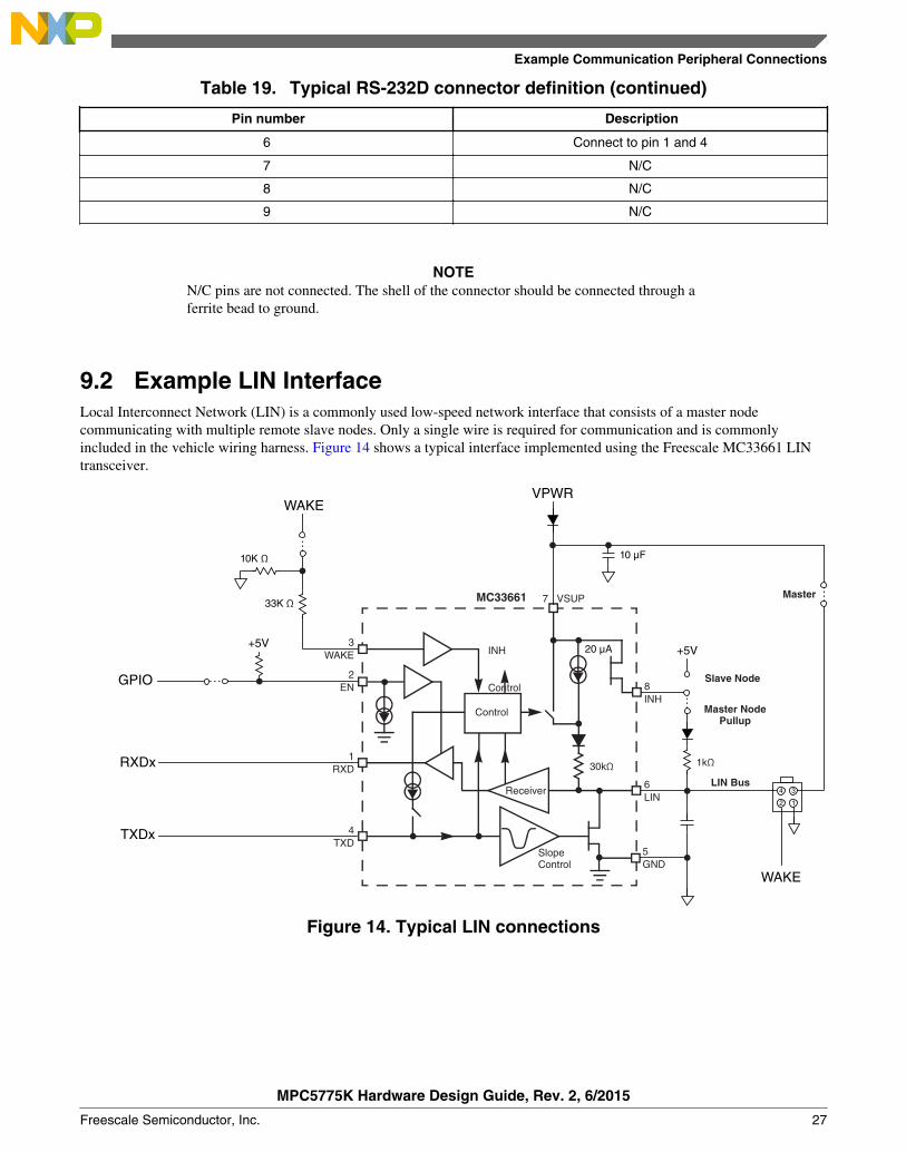
Table 19. Typical RS-232D connector definition (continued)
Pin number Description
6 Connect to pin 1 and 4
7 N/C
8 N/C
9 N/C
NOTEN/C pins are not connected. The shell of the connector should be connected through aferrite bead to ground.
9.2 Example LIN InterfaceLocal Interconnect Network (LIN) is a commonly used low-speed network interface that consists of a master nodecommunicating with multiple remote slave nodes. Only a single wire is required for communication and is commonlyincluded in the vehicle wiring harness. Figure 14 shows a typical interface implemented using the Freescale MC33661 LINtransceiver.
Control
Receiver
INH
Control
5 GND
7 VSUPMC33661
LIN Bus
Master Node Pullup
RXDx
TXDx
VPWR
33K Ω
+5V
10K Ω
GPIO
+5V
Slave Node
12
34
WAKE
WAKE
Master
3 WAKE
2 EN
1 RXD
4 TXD
6 LIN
8 INH
30kΩ
Slope Control
20 μA
10 μF
1kΩ
Figure 14. Typical LIN connections
Example Communication Peripheral Connections
MPC5775K Hardware Design Guide, Rev. 2, 6/2015
Freescale Semiconductor, Inc. 27

Table 20 below shows the pins of the MC33661 and their typical connections to an MCU.
Table 20. MC33661 pin definitions and example system connections
Pin number Pin name Pin direction Full pin name MCU or systemconnection
Description
1 RXD Output Receive DataOutput
MCU LIN RXD LIN Receive DataOutput to the MCU
2 EN Input Enable Control MCU GPIO Enables operationof the device
3 Wake Input Wake Input LIN Bus Wake1 Wake enables thedevices out ofsleep mode
4 TXD Input Transmit Data Input MCU LIN TXD LIN Transmit DataInput from the MCU
5 GND Input Ground System GroundReference
Device groundreference
6 LIN Input/Output LIN Bus LIN bus Bidirectional pinthat represents thesingle-wire transmit
and receiver
7 VSUP Input Power Supply Protected batteryvoltage
This is the powersupply for thedevice and is
typically connectedto a nominal 12 V
8 INH Output Inhibit Output LIN Bus (if master) The Inhibit pincontrols either anexternal regulatorto turn on a slave
node or isconnected througha resistor to the LIN
bus on masternodes
1. Wake is an optional signal on the LIN connector, but may come directly from a switch.
There is no standard industry-defined LIN connector. Freescale uses a 4-pin Molex® connector that allows for the LIN buspin, a power supply source (VPWR), a wakeup signal, and a ground reference. Slave nodes will often implement twoconnectors to allow a daisy-chain of multiple nodes to be easily implemented. Table 21 shows the Freescale pinout.
Table 21. LIN connector pinout recommendation
Function Pin number Pin number Function
LIN Bus 4 3 VPWR
Wake 2 1 Ground
In a typical system, these pins would be used as follows:
• LIN bus—This is the single-wire LIN bus that connects between the master LIN node and the slave LIN nodes.• VPWR—This connector input can be used as the power input to a slave node. Care should be taken that sufficient
current is available for the total number of LIN slaves that are powered through this connection. In some systems, thismay come from the master LIN node.
Example Communication Peripheral Connections
MPC5775K Hardware Design Guide, Rev. 2, 6/2015
28 Freescale Semiconductor, Inc.

• Wake—The Wake signal is typically used for each individual slave node to enable the LIN physical interface of thatnode and to consequently enable the power supply (using the INH output) to power up the MCU to perform someaction. For example, when the handle on a car door is lifted, to turn on the MCU that controls a function inside thevehicle, such as powering a smart dome light or enabling the controls of a smart seat.
• Ground—Ground reference for the module.
Part numbers for the 4-pin Molex Mini-Fit Jr.™ connector are shown in Table 22.
Table 22. Recommended connector part numbers
Description Manufacturer part number(Molex)
4-pin right-angle connector with flange for target system, tin contacts, with latch 39-29-1048
4-pin right-angle connector with pegs for target system, tin contacts, with latch 39-30-1040
4-pin vertical connector with pegs for target system, tin contacts, with latch 39-29-9042
4-pin right-angle connector with flange for target system, gold contacts, latch 39-29-5043
Mating connector with latch for cable assemblies 39-01-2040
Socket terminal for mating cable assembly 39-00-0077
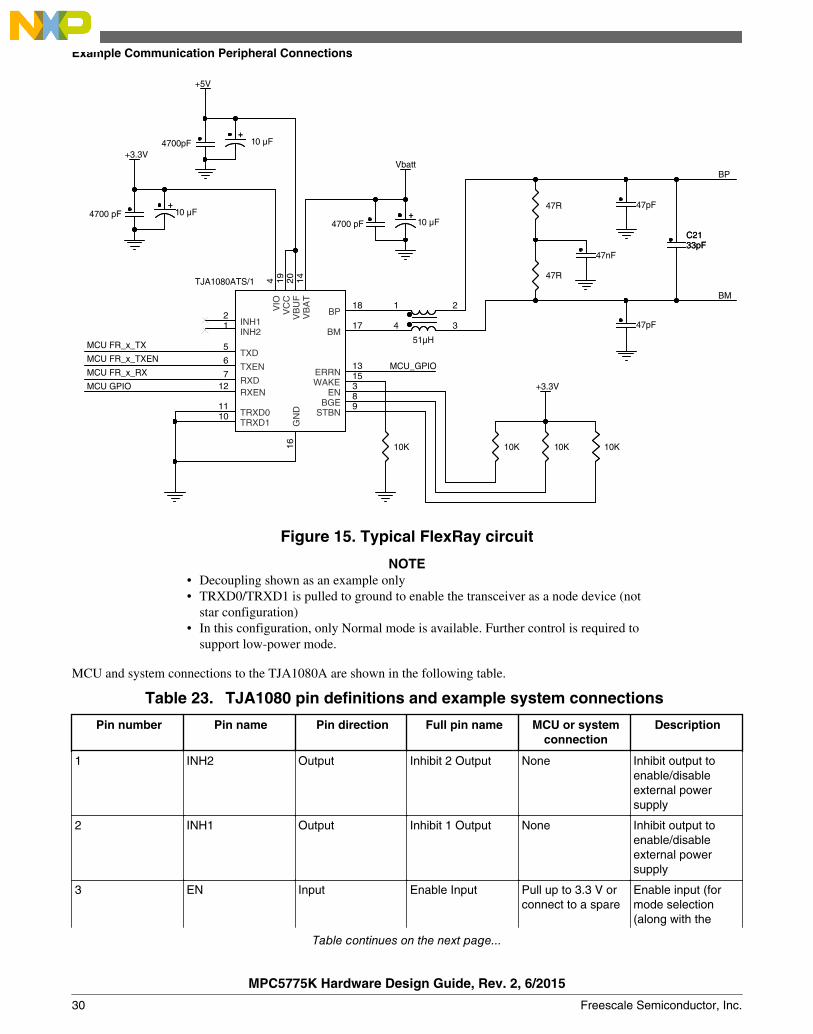
9.3 FlexRay Interface Circuitry using TJA1080AFlexRay is an automotive fault-tolerant 2-wire communications interface. FlexRay is generally used at 10,000 Kbit/s (10Mbit/s).
Freescale FlexRay devices implement a bus driver interface compliant with Communications System Electrical PhysicalLayer Specification, Version 2.1 Rev A.
Typically, FlexRay bus data rates of 10 Mbit/s, 8 Mbit/s, 5 Mbit/s, and 2.5 Mbit/s are supported and although the logicportions of the interface are implemented in the device, an external physical interface device is required to allow multipleFlexRay modules to be connected together.
The NXP™ (http://www.nxp.com ) TJA1080A device is typically used as the FlexRay transceiver, although others areavailable. One transceiver is required for each FlexRay channel. The figure below shows the typical connections using theTJA1080A.
Example Communication Peripheral Connections
MPC5775K Hardware Design Guide, Rev. 2, 6/2015
Freescale Semiconductor, Inc. 29
MCU FR_x_TX
MCU FR_x_TXEN
MCU FR_x_RX
MCU GPIO
MCU_GPIO
BP
BM
Vbatt
+5V
+3.3V
+3.3V
+10 μF
+
10K
47R
47nF
4700 pF
10K
C21 33pFC21 33pF
+10 μF
+
4700pF
47R
++10 μF
47pF
TJA1080ATS/1
TRXD0 11
TRXD1 10
TXD 5
TXEN 6
BGE 8
STBN 9
EN 3WAKE 15
INH2 1 INH1 2 BP
18
BM 17
RXD 7 ERRN
13
RXEN 12
VIO
4
VC
C
19
VB
UF
20
VB
AT
14
GN
D
16
47pF
10K
4700 pF
51μH
21
4 3
10K
Figure 15. Typical FlexRay circuit
NOTE• Decoupling shown as an example only• TRXD0/TRXD1 is pulled to ground to enable the transceiver as a node device (not
star configuration)• In this configuration, only Normal mode is available. Further control is required to
support low-power mode.
MCU and system connections to the TJA1080A are shown in the following table.
Table 23. TJA1080 pin definitions and example system connections
Pin number Pin name Pin direction Full pin name MCU or systemconnection
Description
1 INH2 Output Inhibit 2 Output None Inhibit output toenable/disableexternal powersupply
2 INH1 Output Inhibit 1 Output None Inhibit output toenable/disableexternal powersupply
3 EN Input Enable Input Pull up to 3.3 V orconnect to a spare
Enable input (formode selection(along with the
Table continues on the next page...
Example Communication Peripheral Connections
MPC5775K Hardware Design Guide, Rev. 2, 6/2015
30 Freescale Semiconductor, Inc.
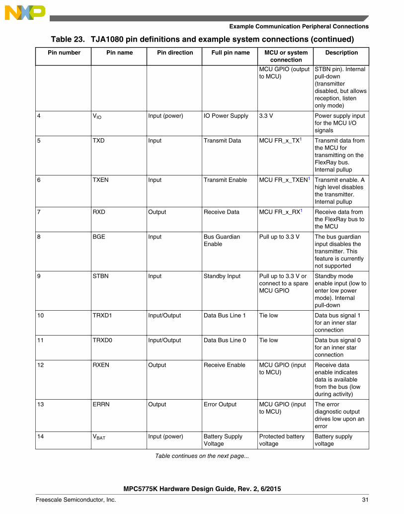
Table 23. TJA1080 pin definitions and example system connections (continued)
Pin number Pin name Pin direction Full pin name MCU or systemconnection
Description
MCU GPIO (outputto MCU)
STBN pin). Internalpull-down(transmitterdisabled, but allowsreception, listenonly mode)
4 VIO Input (power) IO Power Supply 3.3 V Power supply inputfor the MCU I/Osignals
5 TXD Input Transmit Data MCU FR_x_TX1 Transmit data fromthe MCU fortransmitting on theFlexRay bus.Internal pullup
6 TXEN Input Transmit Enable MCU FR_x_TXEN1 Transmit enable. Ahigh level disablesthe transmitter.Internal pullup
7 RXD Output Receive Data MCU FR_x_RX1 Receive data fromthe FlexRay bus tothe MCU
8 BGE Input Bus GuardianEnable
Pull up to 3.3 V The bus guardianinput disables thetransmitter. Thisfeature is currentlynot supported
9 STBN Input Standby Input Pull up to 3.3 V orconnect to a spareMCU GPIO
Standby modeenable input (low toenter low powermode). Internalpull-down
10 TRXD1 Input/Output Data Bus Line 1 Tie low Data bus signal 1for an inner starconnection
11 TRXD0 Input/Output Data Bus Line 0 Tie low Data bus signal 0for an inner starconnection
12 RXEN Output Receive Enable MCU GPIO (inputto MCU)
Receive dataenable indicatesdata is availablefrom the bus (lowduring activity)
13 ERRN Output Error Output MCU GPIO (inputto MCU)
The errordiagnostic outputdrives low upon anerror
14 VBAT Input (power) Battery SupplyVoltage
Protected batteryvoltage
Battery supplyvoltage
Table continues on the next page...
Example Communication Peripheral Connections
MPC5775K Hardware Design Guide, Rev. 2, 6/2015
Freescale Semiconductor, Inc. 31
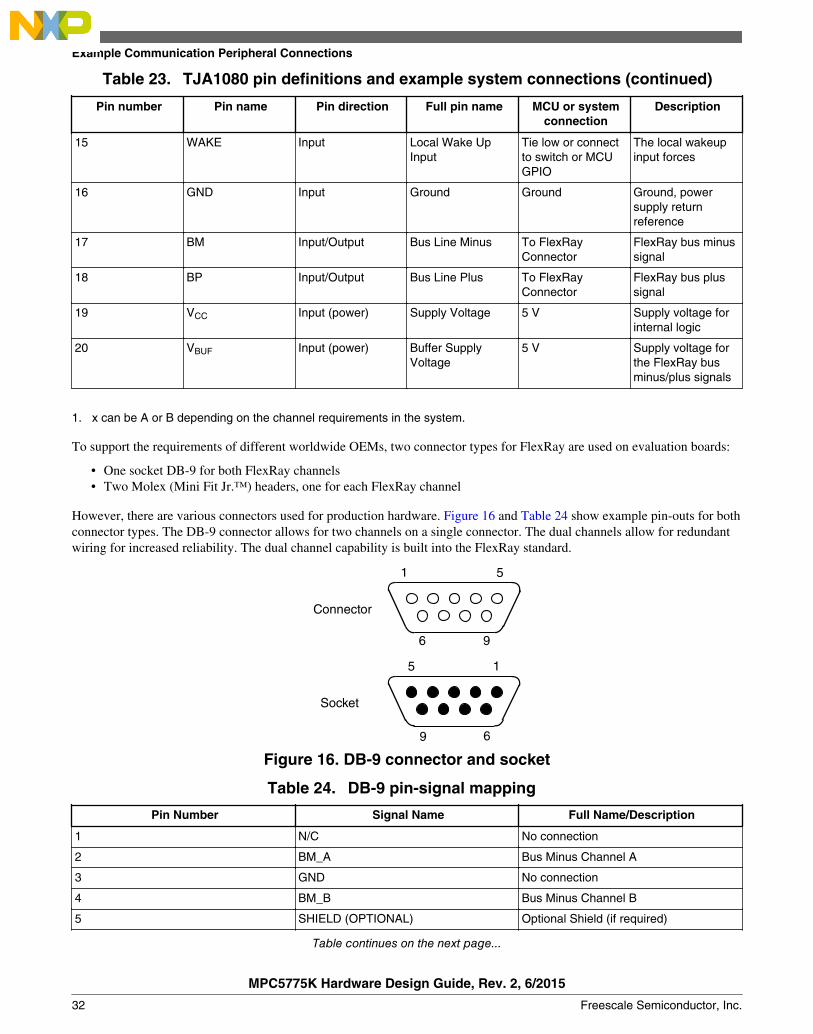
Table 23. TJA1080 pin definitions and example system connections (continued)
Pin number Pin name Pin direction Full pin name MCU or systemconnection
Description
15 WAKE Input Local Wake UpInput
Tie low or connectto switch or MCUGPIO
The local wakeupinput forces
16 GND Input Ground Ground Ground, powersupply returnreference
17 BM Input/Output Bus Line Minus To FlexRayConnector
FlexRay bus minussignal
18 BP Input/Output Bus Line Plus To FlexRayConnector
FlexRay bus plussignal
19 VCC Input (power) Supply Voltage 5 V Supply voltage forinternal logic
20 VBUF Input (power) Buffer SupplyVoltage
5 V Supply voltage forthe FlexRay busminus/plus signals
1. x can be A or B depending on the channel requirements in the system.
To support the requirements of different worldwide OEMs, two connector types for FlexRay are used on evaluation boards:
• One socket DB-9 for both FlexRay channels• Two Molex (Mini Fit Jr.™) headers, one for each FlexRay channel
However, there are various connectors used for production hardware. Figure 16 and Table 24 show example pin-outs for bothconnector types. The DB-9 connector allows for two channels on a single connector. The dual channels allow for redundantwiring for increased reliability. The dual channel capability is built into the FlexRay standard.
1 5
6 9
Connector
15
69
Socket
Figure 16. DB-9 connector and socket
Table 24. DB-9 pin-signal mapping
Pin Number Signal Name Full Name/Description
1 N/C No connection
2 BM_A Bus Minus Channel A
3 GND No connection
4 BM_B Bus Minus Channel B
5 SHIELD (OPTIONAL) Optional Shield (if required)
Table continues on the next page...
Example Communication Peripheral Connections
MPC5775K Hardware Design Guide, Rev. 2, 6/2015
32 Freescale Semiconductor, Inc.

Table 24. DB-9 pin-signal mapping (continued)
Pin Number Signal Name Full Name/Description
6 N/C No connection
7 BP_A Bus Plus Channel A
8 BP_B Bus Plus Channel B
9 N/C No connection
NOTE• A socket is used on the evaluation board and a cable with a connector connects
with this.• The metal shell of the socket should be connected through a ferrite bead to GND.
2
1
Latch Tab
Figure 17. Molex connector picture
Table 25. Molex pin-signal mapping
Pin Number Signal Name
1 BP
2 BM
NOTE
A connector is used on the evaluation board and a cable with a socket connects with this.
The Molex connectors are available in two types, one with pegs for mounting to the board and one without. The part numbersare shown in the following table.
Table 26. Recommended Molex Mini-Fit Jr. connector part numbers
Description Manufacturer Part Number (Molex)
2-pin vertical connector with pegs for target system, tincontacts, latch
39-29-9022
2-pin vertical connector without pegs for target system, tincontacts, latch
39-28-8020
2-pin right-angle connector with pegs for target system, tincontacts, latch
39-30-0020
Table continues on the next page...
Example Communication Peripheral Connections
MPC5775K Hardware Design Guide, Rev. 2, 6/2015
Freescale Semiconductor, Inc. 33

Table 26. Recommended Molex Mini-Fit Jr. connector part numbers (continued)
Description Manufacturer Part Number (Molex)
2-pin right-angle connector with flange for target system, tincontacts, latch
39-29-1028
Mating connector with latch for cable assemblies 39-01-2020
Socket terminal for mating cable assembly 39-00-0077
9.4 CAN Interface CircuitryController Area Network (CAN) is commonly used in almost all automotive applications to allow communication betweenvarious microchips in the car.
The number of CAN modules on-chip varies from device to device. A separate CAN transceiver is required for each CANmodule, although some CAN transceivers may have more than one transceiver on a single chip. It is possible to connect twoCAN modules to a single transceiver if the transmit pins are put into open-collector mode with an external pullup resistor.However, the value of this resistor may limit the maximum speed of the CAN module if not sized properly for the speed.
Freescale CAN modules conform to CAN protocol specification version 2.0 B, and the transceivers shown in this applicationnote comply with ISO 11898 physical layer standard.
Typically, CAN is used at either a low speed (5 Kbit/s to 125 Kbit/s) or a high speed (250 Kbit/s to 1 Mbit/s). Powertrainapplications typically use a high speed (HS) CAN interface to communicate between the engine control unit and thetransmission control unit. Body and chassis applications typically use a low speed (LS) CAN interface. In the dashboard of avehicle, there is typically a gateway device that interfaces between HS and LS CAN networks.
Freescale has a high-speed standalone CAN physical interface device with built-in diagnostic capabilities (MC33902), aswell as CAN transceivers integrated with other functions4. Other popular CAN transceivers include the NXP devices shownin the following table. Example TJA1050 HS and TJA1054 LS circuits are shown in this application note.
Table 27. NXP CAN transceiver comparison
TJA1050 TJA1054 TJA1040 TJA1041
Bitrate (Kbit/s) 1000 125 1000 1000
Modes of operation Normal, Listen-only Normal, Standby, Sleep Normal, Standby Normal, Listen-only,Standby, Sleep
9.4.1 High-Speed CAN With Diagnostics: MC33902 InterfaceFor target systems that require full diagnostics of the CAN interface, the Freescale MC33902 high-speed CAN transceiver isavailable. Features of this device are:
• High-speed CAN interface for baud rates of 40 Kbit/s to 1.0 Mbit/s• Compatible with ISO 11898 standard• Single supply from battery• I/O compatible from 2.75 V to 5.5 V via a dedicated input terminal (3.3 V or 5.0 V logic compatible)• Low-power mode with remote CAN wakeup and local wake-up recognition and reporting
4. An example device is the MC33905 that includes a 5 V power supply controller, a CAN transceiver physical interface, anda LIN transceiver physical interface.
Example Communication Peripheral Connections
MPC5775K Hardware Design Guide, Rev. 2, 6/2015
34 Freescale Semiconductor, Inc.

• CAN bus failure diagnostics and TXD/RXD pin monitoring, cold start detection, and wake-up sources reported throughthe ERR pin
• Enhanced diagnostics for bus, TXD, RXD, and supply pins available through pseudo-SPI via existing terminals EN,STBY, and ERR
• Split terminal for bus recessive level stabilization• INH output to control external voltage regulator
A block diagram of this transceiver is shown below.
Differential Receiver
Driver
Driver
2.5 V
Receiver
Pattern Detection
VSUP
CANH
CANL
QH
QL
Rin
Rin
INH
STBY
ERR
VSUP
Logi
c C
ontr
ol /
Inte
rfac
e / P
_SP
I
VIO
5.0 V Regulator
VDD
Failure Detection Buffer
VDD
SPLIT
Monitoring
INH
Wake-up
& Management
WAKE
GND
Detector
control
TXD
RXD
EN
Vio
Thermal
Figure 18. MC33902 block diagram
While a full SPI interface is not available for the diagnostic information, a quasi-SPI interface is available to communicate tothe MCU. This interface is referred to as the P_SPI interface in the MC33902 data sheet.
The figure below shows an example schematic using the MC33902.
Example Communication Peripheral Connections
MPC5775K Hardware Design Guide, Rev. 2, 6/2015
Freescale Semiconductor, Inc. 35
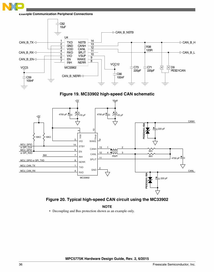
INH 7
TXD 1
RXD 4
EN 6 VIO 5
VDD 3
NERR 8
GND 2
WAKE 9VSUP 10SPLIT 11CANL 12CANH 13NSTB 14 U4
MC33902
CAN_B_TX
CAN_B_RX
CAN_B_H
CAN_B_L
VCC5
C59 100nF
C62 10uF
R38 120R
VCC12
C66 100nF
C73 220pF
C71 220pF
D9 PESD1CAN
CAN_B_EN
CAN_B_NSTB
CAN_B_NERR
Figure 19. MC33902 high-speed CAN schematic
INH
MCU_GPIO or SPI_TXD
MCU_CAN_TX
MCU_CAN_RX CANL
CANH
+5V Vbatt
+5V
220 pF
4700 pF
10KΩ
4700 pF
++ 10 μF
10KΩ P
ES
D24
VL1
BA
PE
SD
24V
L1B
AP
ES
D24
VL1
BA
PE
SD
24V
L1B
A
30Ω
220 pF
4700 pF
30Ω
++ 10 μF
22μH
21
4 3
MC33902
SPLIT 11
CANH 13
CANL 12
STBY 14
WAKE 9
EN 6
VIO 5
INH 7
TXD 1
RXD 4
NERR 8
Vd
d
3
Vsu
p
10
GND 2
MCU_GPIO or SPI_CLKMCU_GPIO or SPI_RXD
Figure 20. Typical high-speed CAN circuit using the MC33902
NOTE• Decoupling and Bus protection shown as an example only.
Example Communication Peripheral Connections
MPC5775K Hardware Design Guide, Rev. 2, 6/2015
36 Freescale Semiconductor, Inc.

The table below shows the pins of the MC33902 and the possible connections to a MCU and the target system.
Table 28. MC33902 pin definitions and example system connections
Pinnumber
Pin name Pindirection
Full pinname
MCU or systemconnection
Description
1 TXD Input TransmitData
MCU CAN TXDA CAN transmit data input from the MCU
2 GND Output Ground Ground Ground termination
3 VDD Output VDDInternalRegulatorOutput
Bypass capacitors only 5 V power supply output. Requiresexternal bypass capacitors.
4 RXD Output ReceiveData
MCU CAN TXDA CAN receive data output to the MCU
5 VIO Input VoltageSupply forIO
3.3 V or 5 V Supply voltage input for the digital inputand output pins. This should be matchedto the IO voltage supply of the MCU.Most typically, this is 5 V, but could alsobe 3.3 V.
6 EN Input Enable Main MCU GPIO or SPItransmit dataoutputeTPUA31 (GPIO)
This is the enable input for the device instatic mode control. This is the masteroutput/slave input when used in SPImode, and the MOSI (master out, slavein) during SPI operation.
7 INH Output Inhibit Use depends on intendedoperation (see text below)
Inhibit output for control of an externalpower supply regulator
8 ERR Output Active LowError
Main MCU GPIO or SPIreceive datainputeTPUA26 (GPIO)
Pin for static error and wakeup flagreporting MISO (master in, slave out)during SPI operation
9 WAKE Input Wake MCU GPIO (output)Tied toground
Wake input
10 VSUP Input VoltageSupply
Battery voltage Battery supply pin, nominally 12 V
11 SPLIT Output Split CAN terminationmidpointNot Used
Output for connection of the CAN bustermination middle point
12 CANL Input/Output CAN BusLow
CAN Bus Connector CAN bus low pin
13 CANH Input/Output CAN BusHigh
CAN Bus Connector CAN bus high pin
14 NTSB Input Standby Main MCU GPIO or SPIClock outputeTPUA28(GPIO)
Standby input for device static modecontrol. CLK (Clock) during P_SPIoperation
The use of the Inhibit pin (INH) is dependent on the selected target system operation. INH can turn an external power supplyon and therefore wake a connected MCU for operation to save power when MCU operation is not required. In MPC5500 andMPC5600 automotive power train applications (engine control), INH is typically not used. However, in automotive body andchassis applications, it may be used.
Example Communication Peripheral Connections
MPC5775K Hardware Design Guide, Rev. 2, 6/2015
Freescale Semiconductor, Inc. 37

9.4.2 High-Speed CAN TJA1050 InterfaceThe figure below shows the typical connections for the physical interface between the MCU and the CAN bus for high-speedapplications using the NXP TJA1050 HS CAN transceiver.
MCU_CAN_TXD
VREF
MCU_CAN_RXD
CANH
CANL
+5V
60 Ω
60 Ω
60 Ω
60 Ω
10K
4700 pF
U1
TJA1050T
U1
TJA1050T
GND 2
VCC 3
CANH 7
CANL 6
S 8
TXD 1
RXD 4
VREF 5
4700 pF
4700 pF
++ 10 μF
Figure 21. Typical high-speed CAN circuit using TJA1050
NOTE• Decoupling shown as an example only.• TXD/RXD pullup/pulldown may be required, depending on device
implementation.
The table below describes the TJA1050 pin and system connections.
Table 29. TJA1050 pin definitions and example system connections
Pinnumber
Pin name Pindirection
Full pinname
MCU or systemconnection
Description
1 TXD Input TransmitData
MCU CAN TXD CAN transmit data input from the MCU
2 GND Output Ground Ground Ground return termination
3 VCC Input — 5 V Voltage supply input (5 V)
4 RXD Output ReceiveData
MCU CAN RXD CAN receive data output to the MCU
5 VREF Output ReferencevoltageOutput
Not used Mid-supply output voltage. This istypically not used in many systems, butcan be used if voltage translation needsto be done between the CAN transceiverand the MCU.
6 CANL Input/Output CAN BusLow
CAN Bus Connector CAN bus low pin
7 CANH Input/Output CAN BusHigh
CAN Bus Connector CAN bus high pin
Table continues on the next page...
Example Communication Peripheral Connections
MPC5775K Hardware Design Guide, Rev. 2, 6/2015
38 Freescale Semiconductor, Inc.

Table 29. TJA1050 pin definitions and example system connections (continued)
Pinnumber
Pin name Pindirection
Full pinname
MCU or systemconnection
Description
8 S Input Select Grounded or MCU GPIO Select for high-speed mode or silentmode. Silent mode disables thetransmitter, but keeps the rest of thedevice active. This may be used in caseof an error condition.
9.4.3 Low-Speed CAN TJA1054 InterfaceThe figure below shows the typical connections for the physical interface between the MCU and the CAN bus for low-speedapplications using the NXP TJA1054 LS CAN transceiver. Optionally, the standby and enable pins can be connected to MCUGPIO pins for additional control of the physical interface.
MCU_CAN_TXDMCU_CAN_RXD
MCU_GPIO
INHCANH
CANL
Vbatt +5V
+5V
10K Ω
10K ΩTJA1054
INH 1
WAKE7
STB5
EN 6
TXD 2
ERR4
RXD 3
GN
D
13
RTL 9
CANH 11
CANL 12
RTH 8
BA
T
14
VC
C
10
4700 pF++
10 μF
4700 pF++
10 μF
511 Ω120 Ω
511 ΩMCU_GPIO
MCU_GPIO
Isolation and protection circuitry is not shown in this drawing,only a termination resistor is shown.
Figure 22. Typical low-speed CAN circuit using TJA1054
NOTE• Decoupling shown as an example only.• STB and EN should be pulled high for Normal mode. These signals can optionally
be connected to MCU GPIO pins to allow MCU control of the physical interface.
Example Communication Peripheral Connections
MPC5775K Hardware Design Guide, Rev. 2, 6/2015
Freescale Semiconductor, Inc. 39
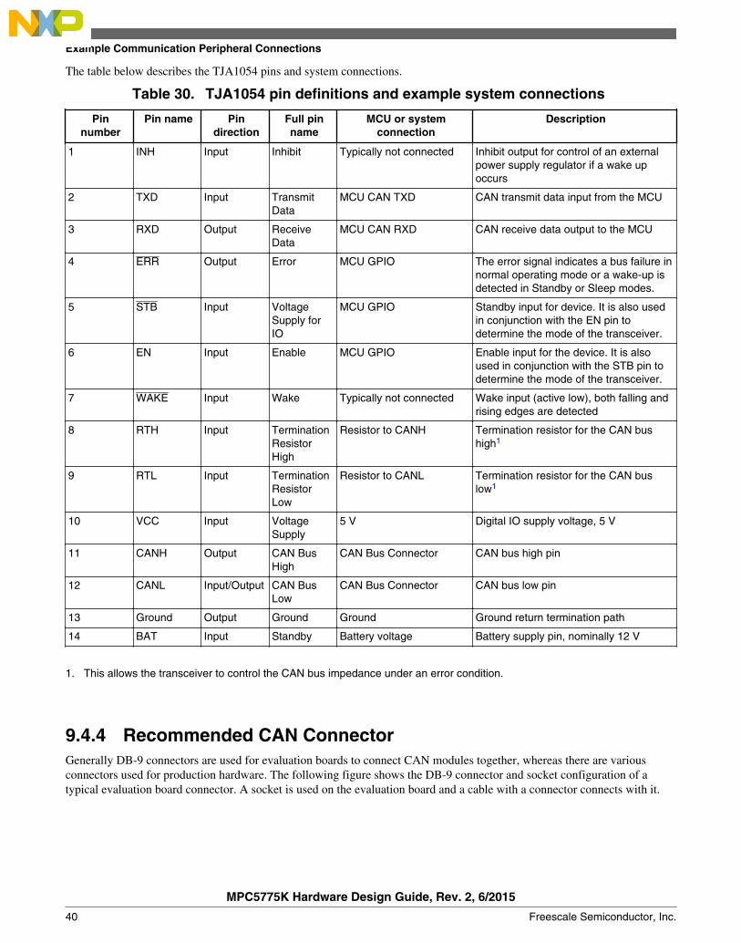
The table below describes the TJA1054 pins and system connections.
Table 30. TJA1054 pin definitions and example system connections
Pinnumber
Pin name Pindirection
Full pinname
MCU or systemconnection
Description
1 INH Input Inhibit Typically not connected Inhibit output for control of an externalpower supply regulator if a wake upoccurs
2 TXD Input TransmitData
MCU CAN TXD CAN transmit data input from the MCU
3 RXD Output ReceiveData
MCU CAN RXD CAN receive data output to the MCU
4 ERR Output Error MCU GPIO The error signal indicates a bus failure innormal operating mode or a wake-up isdetected in Standby or Sleep modes.
5 STB Input VoltageSupply forIO
MCU GPIO Standby input for device. It is also usedin conjunction with the EN pin todetermine the mode of the transceiver.
6 EN Input Enable MCU GPIO Enable input for the device. It is alsoused in conjunction with the STB pin todetermine the mode of the transceiver.
7 WAKE Input Wake Typically not connected Wake input (active low), both falling andrising edges are detected
8 RTH Input TerminationResistorHigh
Resistor to CANH Termination resistor for the CAN bushigh1
9 RTL Input TerminationResistorLow
Resistor to CANL Termination resistor for the CAN buslow1
10 VCC Input VoltageSupply
5 V Digital IO supply voltage, 5 V
11 CANH Output CAN BusHigh
CAN Bus Connector CAN bus high pin
12 CANL Input/Output CAN BusLow
CAN Bus Connector CAN bus low pin
13 Ground Output Ground Ground Ground return termination path
14 BAT Input Standby Battery voltage Battery supply pin, nominally 12 V
1. This allows the transceiver to control the CAN bus impedance under an error condition.
9.4.4 Recommended CAN ConnectorGenerally DB-9 connectors are used for evaluation boards to connect CAN modules together, whereas there are variousconnectors used for production hardware. The following figure shows the DB-9 connector and socket configuration of atypical evaluation board connector. A socket is used on the evaluation board and a cable with a connector connects with it.
Example Communication Peripheral Connections
MPC5775K Hardware Design Guide, Rev. 2, 6/2015
40 Freescale Semiconductor, Inc.

1 5
6 9
Connector
15
69
Socket
Figure 23. DB-9 connector and socket
The table below shows the typical connector pin-out definition.
Table 31. DB-9 pin signal mapping
Pin number Signal name
1 N/C
2 CAN_L
3 GND
4 N/C
5 CAN_SHIELD (OPTIONAL)
6 GND
7 CAN_H
8 N/C
9 CAN_V+ (OPTIONAL)
NOTE
The metal shell of the socket should be connected through a ferrite bead to the chassisground.
9.5 Ethernet Interface ExamplesEthernet is a communication technology that was originally developed for creating local area networks (LANs) betweencomputers. Over time, it has become the standard wired communications network for the PC and is widely used withintelecommunications and industrial applications. In recent years, Ethernet has found its way into automotive electronics withdeployment in diagnostic and camera applications.
The Ethernet MAC-NET (ENET) module on the MPC5775K device is a communication controller that supports 10 and 100Mbit/s Ethernet/IEEE 802.3 networks. It includes functionality to accelerate the processing of various common network layerprotocols such as IP, TCP and UDP. An external transceiver interface and transceiver function are required to complete theinterface to the media. The figure below shows a typical set up of the compete interface to the network. Here a DP83848VYBfrom Texas Instruments is used as the ethernet physical transceiver (PHY). This will be used throughout Ethernet InterfaceExamples to show an example interface.
Example Communication Peripheral Connections
MPC5775K Hardware Design Guide, Rev. 2, 6/2015
Freescale Semiconductor, Inc. 41

MPC5775K
MCU
DP83848VYBMII / RMII
MII- 25MHzRMII - 50MHz Clock Source
ETHERNET PHY
MA
GN
ET
ICS
RJ4510/100 Mb/sE
NE
T
Figure 24. Ethernet application configuration example
As shown in Figure 24 the ENET can interface to a PHY using either the 10/100 Mbit/s MII or RMII or the 10 Mbit/s onlyMII-Lite/7-wire interface. The ENET signals from the MCU take their voltage level from the VDD_HV_IO supply domain.Most PHYs require signals in the 3.3 V range, so the VDD_HV_IO should be set accordingly. Be aware that this domain isshared with the FlexRay I/O.
The ENET signals are summarized in Table 32 and their use in each interface type is highlighted as REQ = Required, N/A =Not applicable for this mode and OPN = Optional.
NOTEThe signals required by different PHYs will vary in some cases for each interface option;see the data sheet of your selected PHY.
Table 32. MPC5775K ENET signal overview
Signal Name Description Direction MII RMII 7-Wire Port Options
ENET_MDIO Management Data Input/Output
I/O REQ N/A N/A PG[8]
ENET_MDC Management Data Clock O REQ N/A N/A PG[9]
ENET_RMII_CLK RMII Reference Clock Input/Output
I/O N/A REQ N/A PG[11]
ENET_TX_EN Transmit Enable O REQ REQ REQ PC[15], PI[3]
ENET_TXD0 Transmit Data 0 O REQ REQ REQ PD[0], PG[3]
ENET_TXD1 Transmit Data 1 O REQ REQ N/A PD[3], PG[4]
ENET_TXD2 Transmit Data 2 O REQ N/A N/A PD[4], PG[6]
ENET_TXD3 Transmit Data 3 O REQ N/A N/A PM[5], PG[10]
ENET_TXCLK Transmit Clock I REQ N/A REQ PG[11]
ENET_RXDV Receive Data Valid I REQ REQ N/A PD[2], PI[2]
ENET_RXD0 Receive Data 0 I REQ REQ REQ PD[5]
ENET_RXD1 Receive Data 1 I REQ REQ N/A PD[6]
ENET_RXD2 Receive Data 2 I REQ N/A N/A PH[4]
ENET_RXD3 Receive Data 3 I REQ N/A N/A PH[5]
ENET_RXCLK Receive Clock I REQ N/A REQ PD[1], PH[13]
Example Communication Peripheral Connections
MPC5775K Hardware Design Guide, Rev. 2, 6/2015
42 Freescale Semiconductor, Inc.
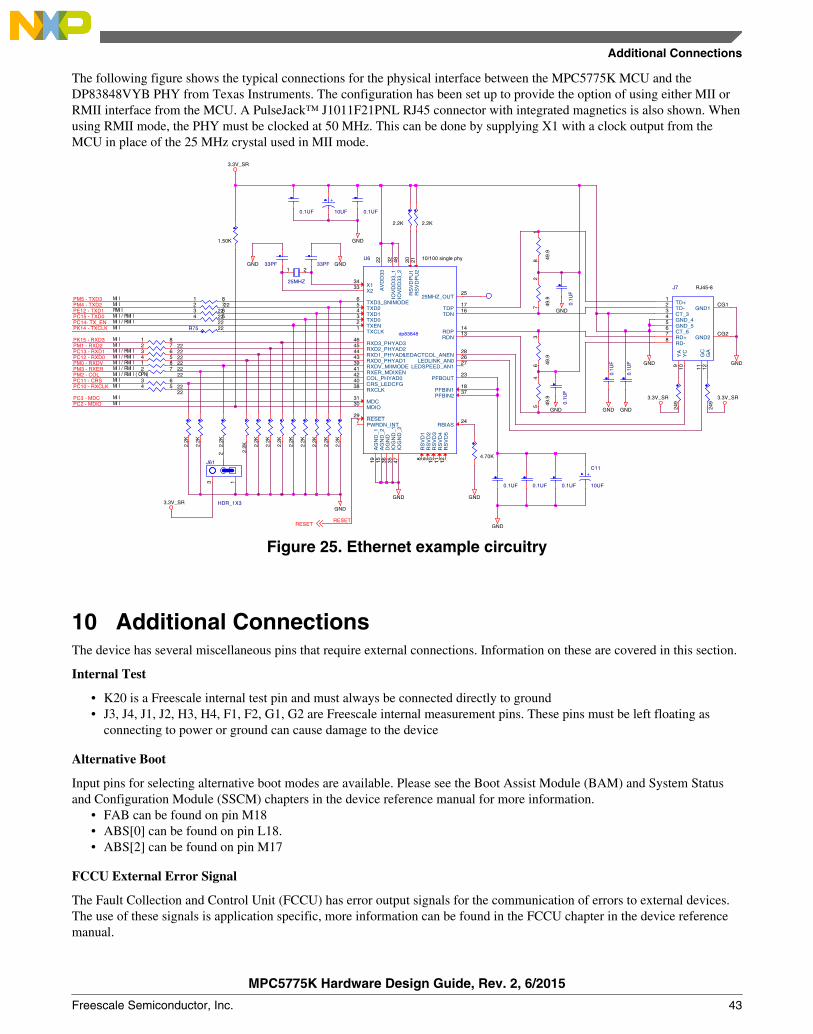
The following figure shows the typical connections for the physical interface between the MPC5775K MCU and theDP83848VYB PHY from Texas Instruments. The configuration has been set up to provide the option of using either MII orRMII interface from the MCU. A PulseJack™ J1011F21PNL RJ45 connector with integrated magnetics is also shown. Whenusing RMII mode, the PHY must be clocked at 50 MHz. This can be done by supplying X1 with a clock output from theMCU in place of the 25 MHz crystal used in MII mode.
PC10 - RXCLK
PK14 - TXCLK
PC15 - TXD0PE12 - TXD1PM4 - TXD2
PK15 - RXD3PM1 - RXD2PC13 - RXD1PC12 - RXD0
PC2 - MDIO
PM0 - RXDVPM3 - RXERPM2 - COLPC11 - CRS
PC14- TX_EN
PC3 - MDC
PM5 - TXD3
RESET
GND
GND
GND
GND GND
GNDGND
3.3V_SR3.3V_SR
GND GND
3.3V_SR
GND
GND
GND
GND3.3V_SR
RESET
RMI I MI I / RMI I MI I / RMI I
MI I
MI I MI I MI I MI I / RMI I ( OPN) MI I / RMI I MI I / RMI I MI I / RMI I MI I / RMI I MI I MI I MI I
MI I MI I
49.9
36
33PF
0.1UF
2.2K
222 7
0.1U
F
J7 RJ45-8
TD+1
TD-2
CT_33
GND_44
GND_55
CT_66
RD+7
RD-8
YA
9
YC
10
GC
11
GA
12
GND1CG1
GND2CG2
25MHZ
21
0.1UF
1.50K
2.2K
2.2K
0.1U
F
0.1UF
2.2K
224 5
249
0.1UF
2.2K
0.1UF
223 6
222 7
49.9
18
2.2K
224 5
221 8
223 6
J61
HDR_1X3
1
2
3
0.1U
F
221 8
0.1U
F
2.2K
2.2K
49.9
27
R75 22
2.2K
dp83848
U6 10/100 single phy
RXCLK38
RS
VD
PU
221
RS
VD
PU
120
RS
VD
512
RS
VD
411
RS
VD
310
RS
VD
29
RS
VD
18
RDN13RDP14
LEDACTCOL_ANEN28
IOV
DD
33_2
48IO
VD
D33
_132
IOG
ND
_247
IOG
ND
_135
DG
ND
36A
VD
D33
22A
GN
D_2
15A
GN
D_1
19
TXD25
TXCLK1
LEDLINK_AN026
RXER_MDIXEN41
MDC31
RESET29
PWRDN_INT7
MDIO30
CRS_LEDCFG40
RXD3_PHYAD346
RXD2_PHYAD245
RXD1_PHYAD144
RXD0_PHYAD143
RXDV_MIIMODE39
TXEN2 TXD03
LEDSPEED_AN127
PFBIN237
TXD3_SNIMODE6
TXD14
RBIAS24
COL_PHYAD042
PFBIN118
PFBOUT23
X233 X134
TDN16TDP17
25MHZ_OUT25
249
2.2K
49.9
45
224 5
+
10UF
33PF
223 6
2.2K
2.2K
222 7
4.70K
221 8
+C11 10UF
2.2K
2.2K
Figure 25. Ethernet example circuitry
10 Additional ConnectionsThe device has several miscellaneous pins that require external connections. Information on these are covered in this section.
Internal Test
• K20 is a Freescale internal test pin and must always be connected directly to ground• J3, J4, J1, J2, H3, H4, F1, F2, G1, G2 are Freescale internal measurement pins. These pins must be left floating as
connecting to power or ground can cause damage to the device
Alternative Boot
Input pins for selecting alternative boot modes are available. Please see the Boot Assist Module (BAM) and System Statusand Configuration Module (SSCM) chapters in the device reference manual for more information.
• FAB can be found on pin M18• ABS[0] can be found on pin L18.• ABS[2] can be found on pin M17
FCCU External Error Signal
The Fault Collection and Control Unit (FCCU) has error output signals for the communication of errors to external devices.The use of these signals is application specific, more information can be found in the FCCU chapter in the device referencemanual.
Additional Connections
MPC5775K Hardware Design Guide, Rev. 2, 6/2015
Freescale Semiconductor, Inc. 43

• FCCU_F0 can be found on Y15• FCCU_F1 can be found on W15
Non-Maskable Interrupt (NMI)
NMI input can be found on pin Y18. The use of this pin is application specific; please see the Wake-up Unit (WKPU) chapterin the device reference manual for more information.
If the pin is not used, it can be rendered non-functional by connecting to VDD_HV_IO through a 4.7 Kilo Ohm or 10 KiloOhm pull-up resistor.
No Connection Pins
There are a number of non-functional pins that must be dealt with appropriately.
Table 33. No connection pins
Pins No Connect Strategy
d3 Connect to ground (GND)
r19, r20 Connect to ground (GND)
t4 Leave floating
t18, t19 Connect to ground (GND)
u3 Leave floating
u10 Connect to ground (GND)
v10 Connect to ground (GND)
k20 Connect to ground (GND)
Appendix A Release NotesTable A-1 summarizes revisions to this document.
Table A-1. Revision History
Rev Date Description of Changes
1 3/2015 • In section Power Supply removed mention of 5V SAR ADC reference option• In section Power Supply Signals and Decoupling
• Removed mention of 5V SAR ADC reference option• Consolidated VDD_HV_PDI pins• Changed name of VDD_LV_DRFPLL to VDD_LV_LFASTPLL and added explanation note• Changed recommended capacitance configurations for supply pin decoupling
• In section Decoupling Capacitors Layout Priority added VDD_LV_IO and consolidatedVDD_HV_PDI pins
• In section Power Management Controller• Removed mention of 5V SAR ADC reference option• Modified diagram to remove 5V SAR ADC reference option• Added note describing function of VREG_POR_B
• In section SMPS External Component Configuration added detail to description• In section External Supply Mode
• Removed mention of 5V SAR ADC reference option• Modified diagram to remove 5V SAR ADC reference option
• In section Power-up Sequence added rule on powering VDD_HV_IO and VDD_HV_PMU• In section External Reset Signals added note on VREG_POR_B functionality
Table continues on the next page...
Additional Connections
MPC5775K Hardware Design Guide, Rev. 2, 6/2015
44 Freescale Semiconductor, Inc.
Table A-1. Revision History (continued)
Rev Date Description of Changes
• In section MPC5775K High-Speed Nexus Serial Trace Connector added part number for serialtrace connector
• In section Minimum External Circutiry corrected Nexus clock lines recommended capacitancevalues
• In table AFE external component connections• Changed SD_R trimming resistor tolerance• Corrected function description on VDD_LV_SDADC and VDD_LV_RADARDIG pins
2 6/2015 • In section Power Supply Signals and Decoupling removed VDD_HV_IO_PWM and consolidatedinto VDD_HV_IOx supply.
• Added footnote to VDD_LV_IO_AURORA• In section Power Management Controller modified the supply connections diagrams
• Removed HV_IO_PWM• Combined HV_IO_PDI_0 and HV_IO_PDI_1 into HV_IO_PDI• Removed regulator supplying HV_REG_3V8 and connected this to 3.3 V regulator
• In section Connecting External Clock Sources removed mention of configurable load capacitanceand added advice on parasitic capacitance on oscillator connection lines.
MPC5775K Hardware Design Guide, Rev. 2, 6/2015
Freescale Semiconductor, Inc. 45

How to Reach Us:
Home Page:freescale.com
Web Support:freescale.com/support
Information in this document is provided solely to enable system andsoftware implementers to use Freescale products. There are no expressor implied copyright licenses granted hereunder to design or fabricateany integrated circuits based on the information in this document.Freescale reserves the right to make changes without further notice toany products herein.
Freescale makes no warranty, representation, or guarantee regardingthe suitability of its products for any particular purpose, nor doesFreescale assume any liability arising out of the application or use ofany product or circuit, and specifically disclaims any and all liability,including without limitation consequential or incidental damages.“Typical” parameters that may be provided in Freescale data sheetsand/or specifications can and do vary in different applications, andactual performance may vary over time. All operating parameters,including “typicals,” must be validated for each customer application bycustomer's technical experts. Freescale does not convey any licenseunder its patent rights nor the rights of others. Freescale sells productspursuant to standard terms and conditions of sale, which can be foundat the following address: freescale.com/SalesTermsandConditions.
Freescale™ and the Freescale logo are trademarks of FreescaleSemiconductor, Inc. The Power Architecture and Power.org word marksand the Power and Power.org logos and related marks are trademarksand service marks licensed by Power.org. All other product or servicenames are the property of their respective owners.
© 2015 Freescale Semiconductor, Inc.
Document Number AN4888Revision 2, 6/2015