molecular electronics - eecs · origins of molecular electronics “it seems to us reasonable to...
TRANSCRIPT

Molecular Electronics
11/17/05

- Molecules are used in bulk form in a number of prototype devices:
Thin film transistors, Prof. Kaniki group
Covered by EECS 513: Flat Panel Displays
- Limit our discussion to situation where:• Small number (< ~ 1000) of molecules per device.• Each molecule plays an active role.• further focusing on small organic molecules , macromolecules (eg, carbon nanotubes) already discussed
Molecular electronics: definition
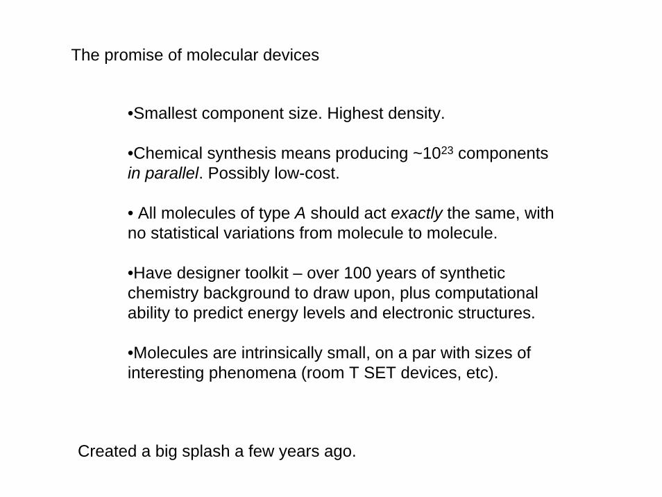
•Smallest component size. Highest density.
•Chemical synthesis means producing ~1023 components in parallel. Possibly low-cost.
• All molecules of type A should act exactly the same, with no statistical variations from molecule to molecule.
•Have designer toolkit – over 100 years of synthetic chemistry background to draw upon, plus computational ability to predict energy levels and electronic structures.
•Molecules are intrinsically small, on a par with sizes of interesting phenomena (room T SET devices, etc).
Created a big splash a few years ago.
The promise of molecular devices

Three key ideas that are fundamental departures from traditional electronics industry methodologies:
Big concepts
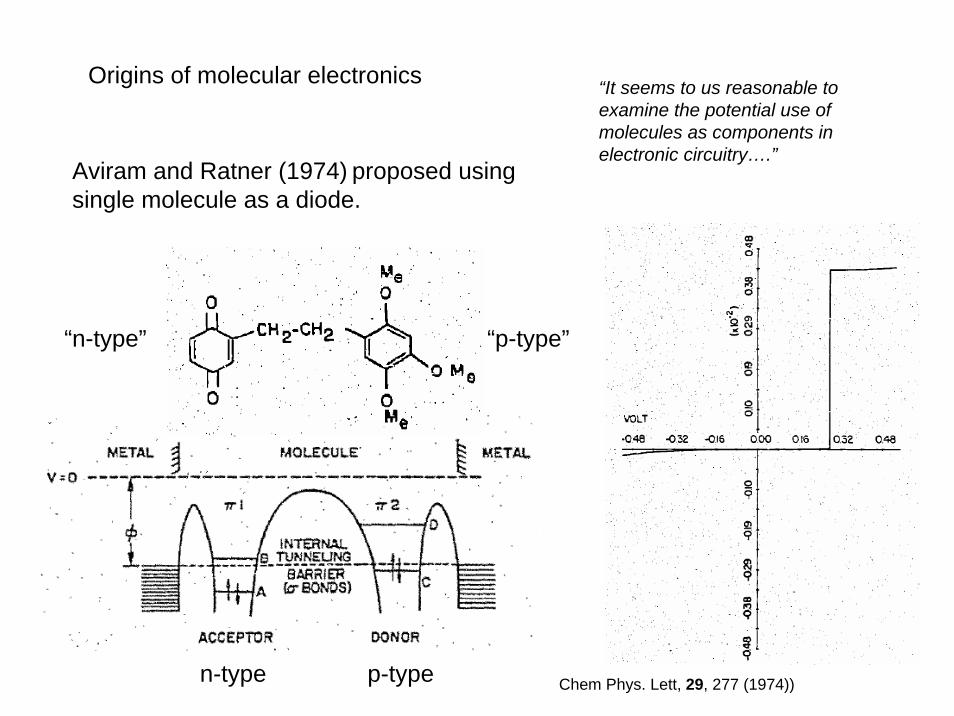
Aviram and Ratner (1974) proposed using single molecule as a diode.
Origins of molecular electronics “It seems to us reasonable toexamine the potential use ofmolecules as components inelectronic circuitry….”
“n-type”
n-type p-type
“p-type”
Chem Phys. Lett, 29, 277 (1974))
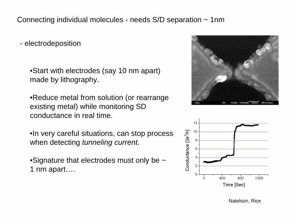
•Start with electrodes (say 10 nm apart) made by lithography.
•Reduce metal from solution (or rearrange existing metal) while monitoring SD conductance in real time.
•In very careful situations, can stop process when detecting tunneling current.
•Signature that electrodes must only be ~ 1 nm apart….
Connecting individual molecules - needs S/D separation ~ 1nm
- electrodeposition
Natelson, Rice

Downsides:
• Long term stability at room temperature poor.
• Cleanliness and microstructure of metal not well characterized or controlled.
• Strong indications that, at atomic scale, deposited metal is not necessarily a good metal!
Bottom line:Hard to attribute observed effects to molecules. Not a good choice.
Electrodeposition
Natelson, Rice

•Start with continuous metal wire.
•(At low T and UHV), flow current through wire until it breaks due to electromigration.
•Resulting in nm size gap.
•Decorate broken wire with molecules.
•Good metal, clean.
•Still have stability problems when sample is raised back up to higher temperatures.
Park et al., APL 75, 301 (1999).Electromigration
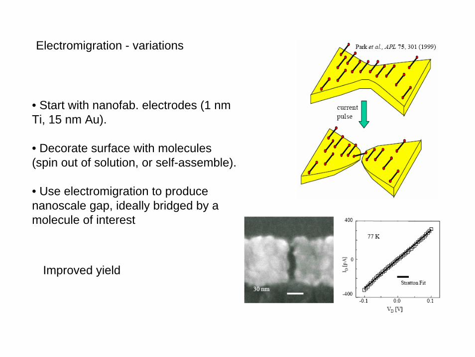
• Start with nanofab. electrodes (1 nmTi, 15 nm Au).
• Decorate surface with molecules(spin out of solution, or self-assemble).
• Use electromigration to producenanoscale gap, ideally bridged by amolecule of interest
Improved yield
Electromigration - variations
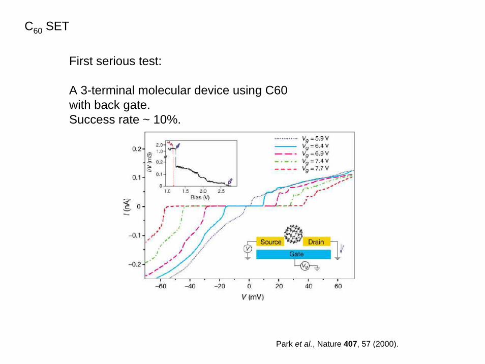
First serious test:
A 3-terminal molecular device using C60 with back gate.Success rate ~ 10%.
Park et al., Nature 407, 57 (2000).
C60 SET

• Coulomb blockade “diamond plot” - changing charge on C60 by 1 electron.• Coupling to gate varies from device to device.• Signature of additional excitation with ~ 5 meVenergy.
Park et al., Nature 407, 57 (2000).

Proposed explanation for that excitation:
Vibrational mode of C60 bound to Au.
Adding or removing an electron excites the vibrationalmodes (forces exerted by image charge)
C60 SET
Devices at this scale, made with not well-controlled methods, are dreadful to debug.
• Low yields of small gaps (10-15%)
• How can you tell what you have? No control of final molecular / metal configuration.
• intentionally reduce device yield (y) to reduce probabilities of having more than one molecules connected (~y2)
• find common features on all possible devices, and neglect effects observed only occasionally (can see just about everything once or twice).
• Use a “designer molecule” that allows you to clearly identify molecular conduction and distinguish it from others
Challenges:
One commonly used trick, thiol (-HS) groups bond well to Au.
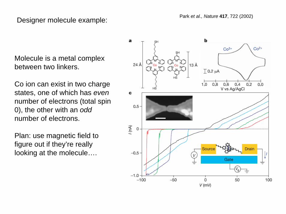
Molecule is a metal complex between two linkers.
Co ion can exist in two charge states, one of which has even number of electrons (total spin 0), the other with an odd number of electrons.
Plan: use magnetic field to figure out if they’re really looking at the molecule….
Designer molecule example: Park et al., Nature 417, 722 (2002)

•“Extra” level appears because “free” spin on Co ion can be either aligned or antialigned with applied magnetic field.
•This level shifts linearly with applied field: Zeeman effect!
•Other evidence: Kondo effect….
Designer molecule example:Park et al., Nature 417, 722 (2002)
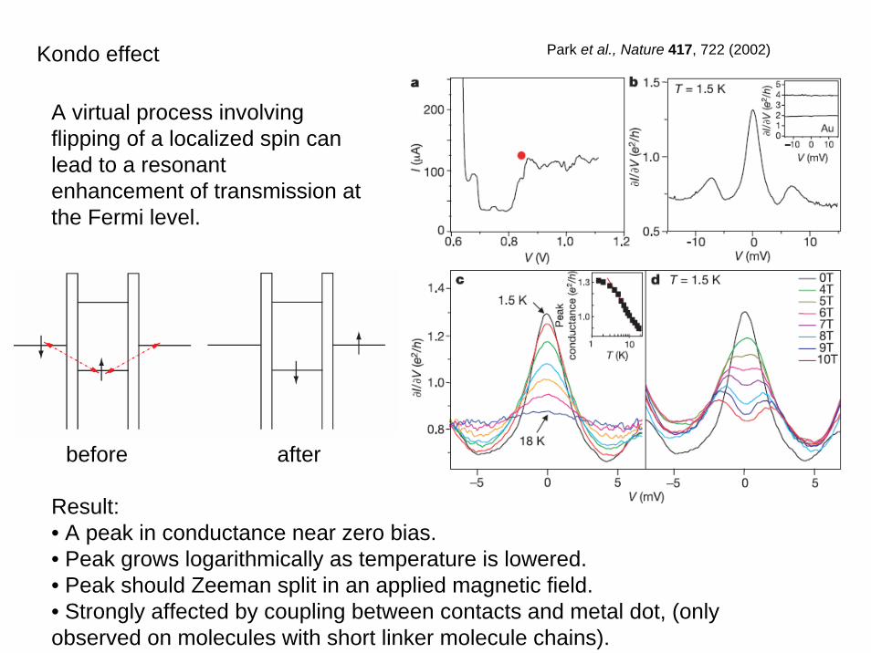
A virtual process involving flipping of a localized spin can lead to a resonant enhancement of transmission at the Fermi level.
Result:• A peak in conductance near zero bias.• Peak grows logarithmically as temperature is lowered.• Peak should Zeeman split in an applied magnetic field.• Strongly affected by coupling between contacts and metal dot, (only observed on molecules with short linker molecule chains).
Kondo effect
before after
Park et al., Nature 417, 722 (2002)

New molecule includestwo vanadiumions that can have eitherspin 0 or spin 1/2depending on charge state.
Plan: Total spin ofmolecule should vary ascharge of molecule isvaried.
Liang et al., Nature 417, 725 (2002)Designer molecule example:

Kondo effect is again observed.
This paper appeared back-to-back in Nature with the previous paper we justdiscussed.
The point of both: strong evidence that they are really looking at transport through a single molecule of interest.
Highest Kondo temperature devices due to the small size of the molecules
Designer molecule example:
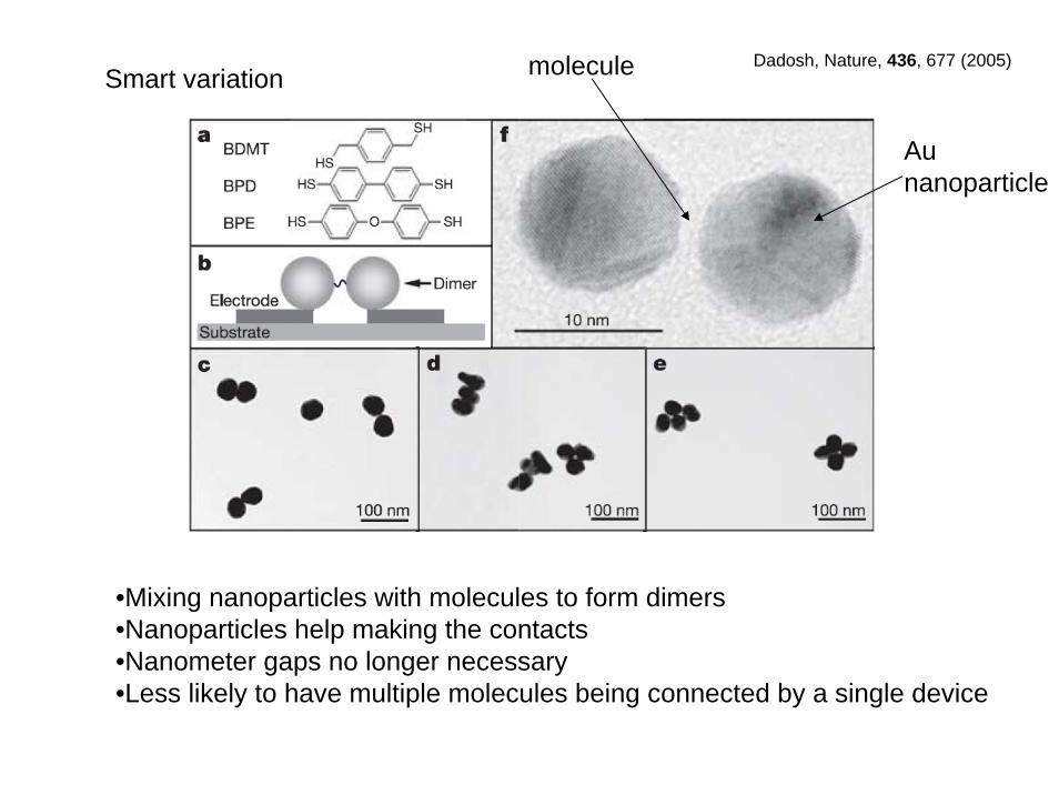
Smart variation
•Mixing nanoparticles with molecules to form dimers•Nanoparticles help making the contacts•Nanometer gaps no longer necessary•Less likely to have multiple molecules being connected by a single device
Dadosh, Nature, 436, 677 (2005)molecule
Au nanoparticle
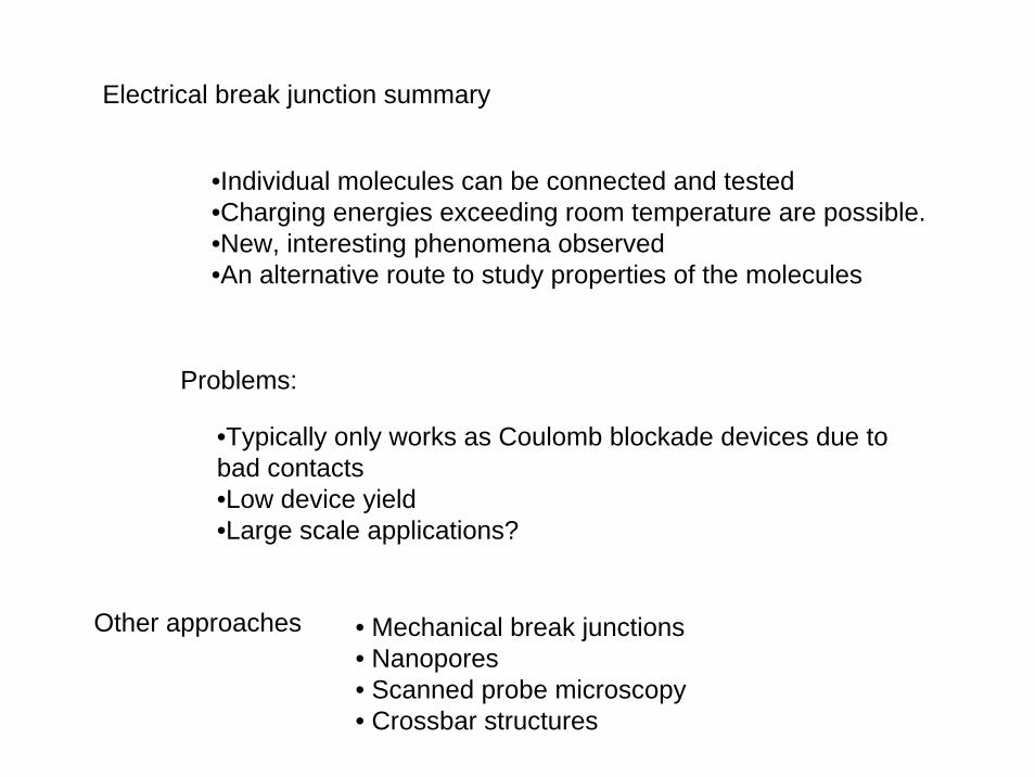
Electrical break junction summary
•Individual molecules can be connected and tested•Charging energies exceeding room temperature are possible.•New, interesting phenomena observed•An alternative route to study properties of the molecules
•Typically only works as Coulomb blockade devices due to bad contacts•Low device yield•Large scale applications?
Problems:
Other approaches • Mechanical break junctions• Nanopores• Scanned probe microscopy• Crossbar structures

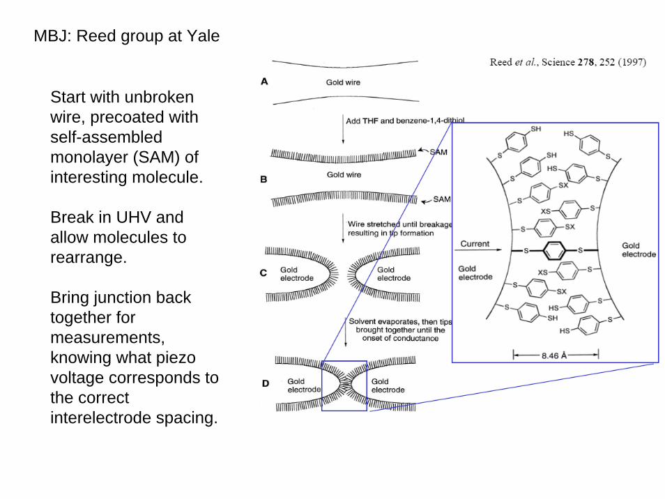
Start with unbroken wire, precoated with self-assembled monolayer (SAM) of interesting molecule.
Break in UHV andallow molecules to rearrange.
Bring junction back together for measurements,knowing what piezovoltage corresponds tothe correct interelectrode spacing.
MBJ: Reed group at Yale

Reed et al., Science 278, 252 (1997)
di Ventra et al., PRL 84, 979 (2000)
Results:
•Differential conductance (blue trace) has features that can be identified with resonant tunneling through molecular levels.
•Theory must account for specific bonding of S to Au to get shape close
•Theory still overestimates conduction by ~ 20x.
MBJ: Reed

• Highly productive research technique for examining single molecules.• Shows that single molecule conduction is possible, though generally poor.• Single molecule conduction depends crucially on atomic-scale details of bonding and metal surfaces.
Problems:
• Mechanical stability essential.• Very difficult to do temperature sweeps - everything moves due to differential contraction. This is a problem b/c standard way of deducing conduction mechanisms uses G(V,T).
MBJ summary

Not a single molecule technique - more like ~ 1000 in parallel.Originally developed to study ~ 10-30 nm diameter metal junctions.

Images from Reed group, Yale
Nanopores
Requires self-assembly followed byevaporation of top electrode.No one knows what interface looks like.Yield very very low (~ 1-2 %).

•Nanopore devices made with above molecule exhibit negative differential resistance, as shown.
•Mechanism not clear: temperature dependence is significant and steep.
•Proposed mechanism: changes in resistance in different charge states
Nanopore devices: NDR
Chen et al., Science 286, 1550 (1999)Seminario et al., JACS 122, 3015 (2000)

With modification of molecule,can see NDR that persists up toroom temperature.
Other possible mechanism besides simple electronic structure:orientation of phenyl rings.
Nanopore devices: NDR
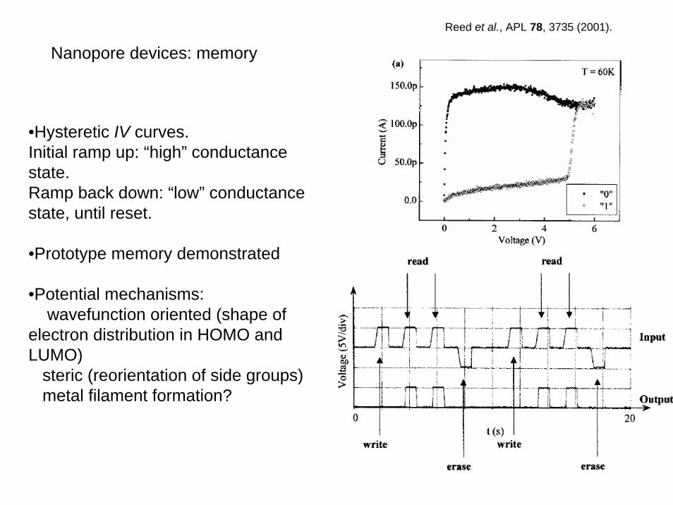
•Hysteretic IV curves. Initial ramp up: “high” conductance state.Ramp back down: “low” conductance state, until reset.
•Prototype memory demonstrated
•Potential mechanisms:wavefunction oriented (shape of
electron distribution in HOMO and LUMO)
steric (reorientation of side groups)metal filament formation?
Nanopore devices: memoryReed et al., APL 78, 3735 (2001).

Another means of looking forinteresting molecules andtesting their (2-terminal)conductive properties is to usescanned probe microscopes.
• Allows highly controlledpositioning of electrodespreviously decorated withmolecules.
• Can obtain I-V curves forsingle molecules.
• Can quickly examine manymolecules
Scanned probe microscopy: STM

• Mechanical stability.
• Difficult to do T-dep. measurements.
• Interpretation of contacts difficult-tunneling conductance is supposed to be proportional to product of local single-particle density of states of tip and surface.
• As result, tricky to deconvolve topography from electronic properties.
One occasion it’s not too hard: time varyingbehavior
Donhauser et al., Science 292, 2303 (2001).
Downsides:
Phenylene ethynylene oligomers isolated in matrices of alkanethiolate monolayers.
Switching caused by conformational changes rather than charge transfer as previously argued.
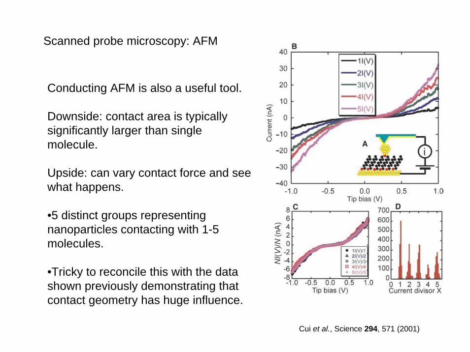
Conducting AFM is also a useful tool.
Downside: contact area is typicallysignificantly larger than singlemolecule.
Upside: can vary contact force and seewhat happens.
•5 distinct groups representing nanoparticles contacting with 1-5 molecules.
•Tricky to reconcile this with the data shown previously demonstrating that contact geometry has huge influence.
Scanned probe microscopy: AFM
Cui et al., Science 294, 571 (2001)

• Nanopores have produced some impressive results - NDR, memory w/ T-dependent measurements of ~ 1000 molecules in ||.
• Problem is, yields are terrible, and diagnostics on final molecule condition is essentially impossible.
• SPM techniques are much faster, and confirm some of the nanopore work (NDR, switching of conductance states).
• Unfortunately, SPM has its own set of experimental issues.
• Mechanisms behind these results still argued.
Nanopore and SPM summary
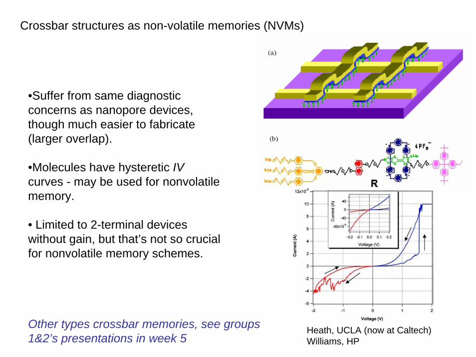
•Suffer from same diagnostic concerns as nanopore devices, though much easier to fabricate (larger overlap).
•Molecules have hysteretic IV curves - may be used for nonvolatile memory.
• Limited to 2-terminal devices without gain, but that’s not so crucial for nonvolatile memory schemes.
Crossbar structures as non-volatile memories (NVMs)
Other types crossbar memories, see groups 1&2’s presentations in week 5
Heath, UCLA (now at Caltech)Williams, HP
Molecular crossbar structures as NVMs
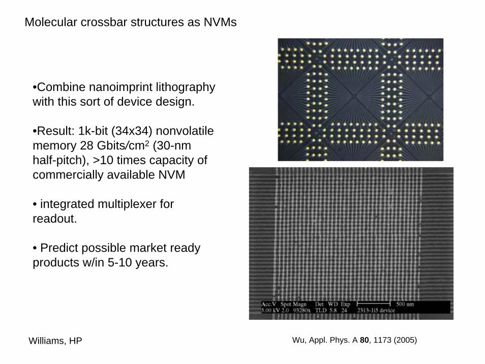
•Combine nanoimprint lithography with this sort of device design.
•Result: 1k-bit (34x34) nonvolatile memory 28 Gbits/cm2 (30-nm half-pitch), >10 times capacity of commercially available NVM
• integrated multiplexer for readout.
• Predict possible market ready products w/in 5-10 years.
Wu, Appl. Phys. A 80, 1173 (2005)Williams, HP
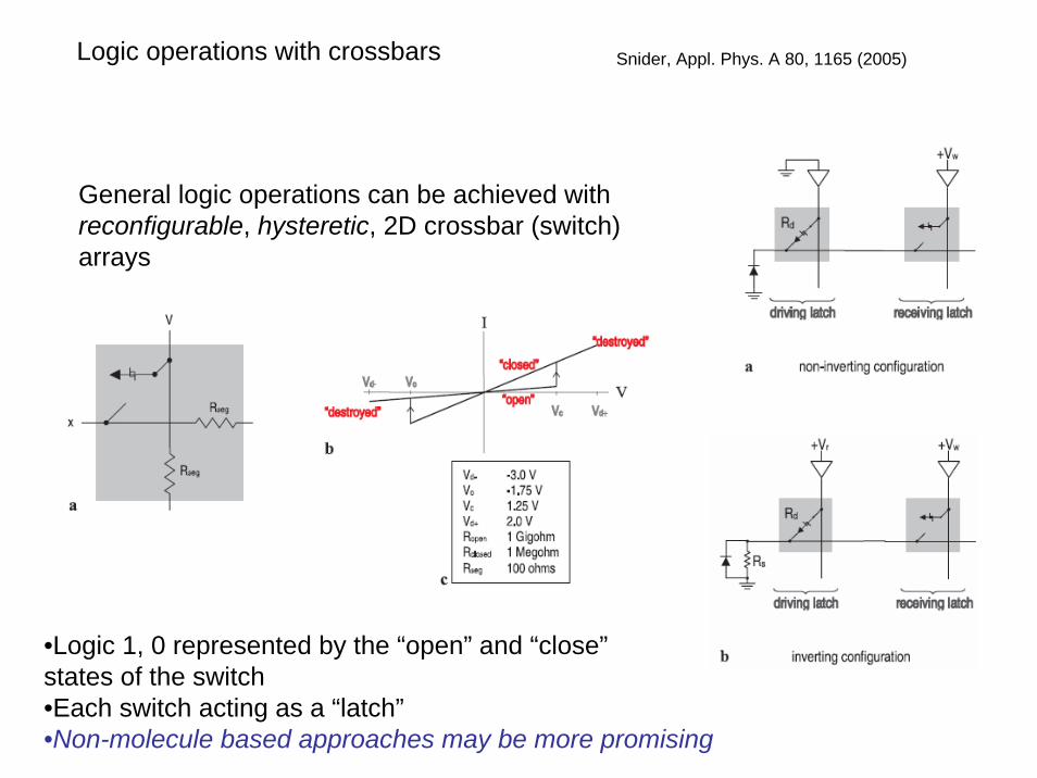
Logic operations with crossbars
General logic operations can be achieved with reconfigurable, hysteretic, 2D crossbar (switch) arrays
•Logic 1, 0 represented by the “open” and “close”states of the switch•Each switch acting as a “latch”•Non-molecule based approaches may be more promising
Snider, Appl. Phys. A 80, 1165 (2005)

Half-adder circuit
Combining multiple crossbars to implement more complex logic functions.
General logic operations Snider, Appl. Phys. A 80, 1165 (2005)

Dealing with defects
Large number of defects in these nanodevices
•Redundancy: instead of trying to make each device perfect, make redundant imperfect devices with high connectivity
•Shifting difficulty in hardware to software: build the generic computer (however imperfectly), find the defects, configure the resources with software, compile the program, and then run it. Think how a field programmable gate array (FPGA) works.
Coding with redundancyHeath, Science ,280, 1716 (1998)Kuekes, Sci Ame, 74, Nov, (2005)

• Self-assemble large number offunctionalized nanoparticles +molecules (e.g. NDR and memorymolecules) across an array of leads.
• Training + field programming:apply voltage pulses; measurecurrents; train system to havedesired functionality (!).
Nanocell concept
Tour (Rice), Reed (Yale)
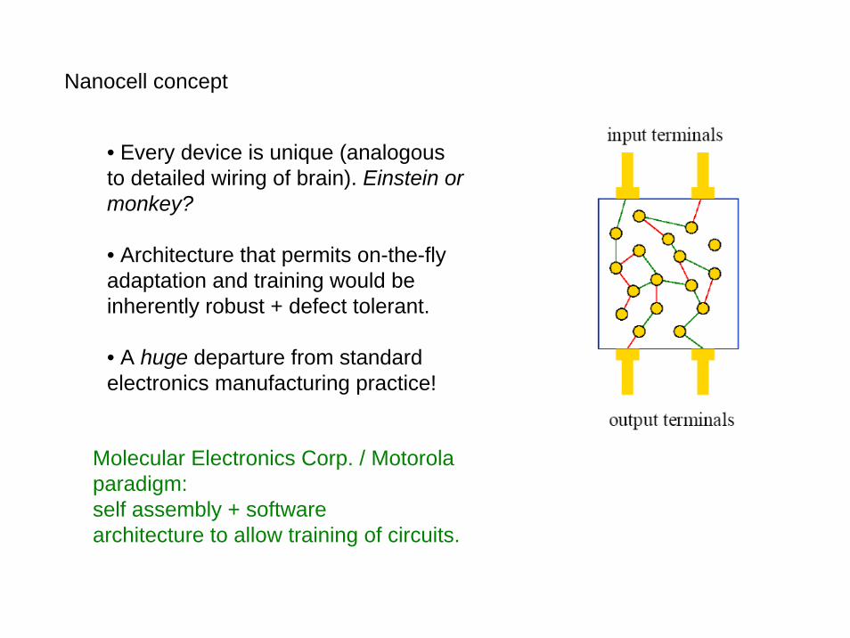
• Every device is unique (analogousto detailed wiring of brain). Einstein or monkey?
• Architecture that permits on-the-flyadaptation and training would beinherently robust + defect tolerant.
• A huge departure from standardelectronics manufacturing practice!
Molecular Electronics Corp. / Motorola paradigm: self assembly + softwarearchitecture to allow training of circuits.
Nanocell concept

• Several research tools exist to study and utilize a single molecule or a small number of molecules.
• Details (contacts, quantitative results with predictive power) are still lacking.
• Basic physics responsible for certain interesting properties (NDR, switching) still under debate.
• We’re a long way from practical molecular electronic devices, though applications in niche markets may be on the horizon.
• Knowledge learned, such as the crossbar structure, may provide a promising solution to past Moor’s law, even though molecular electronics may not be the best choice.
Summary and prospects