dna based molecular electronics -...
TRANSCRIPT

SUBMISSION OF PROJECT PROPOSAL ON RESEARCH AND DEVELOPMENT, PROGRAMME SUPPORT OF DBT
PROJECT TITLE
DNA based Molecular Electronics
SUBMITTED BY
Prof. Rajiv Prakash (Principal Investigator)
Professor
School of Materials Science and Technology,
Institute of Technology, Banaras Hindu University, Varanasi 221005

2
PROFORMA FOR SUBMISSION OF PROJECT PROPOSALS ON RESEARCH AND DEVELOPMENT, PROGRAMME SUPPORT
PART I: GENERAL INFORMATION
1. Name of the Institute/University/Organization submitting the Project Proposal: School of Materials Science and Technology, Institute of Technology, Banaras Hindu University, Varanasi-221005 ……………………………………...........…………………………………………......... 2. State: ...U.P............................. 3. Status of the Institute: Central University ....................................................................... (Please see Annexure-I)(Project Performa downloads in DBT site, Sl. No 20) 4. Name and designation of the Executive Authority of the Institute/University forwarding the application: ........................................................................................................................ ......................Registrar, Banaras Hindu University, Varanasi...................................... ..............................................................………………………………………………….. 5. Project Title:...... DNA based Molecular Electronics..................................................
............................................................................................................................................ 6. Category of the Project (Please tick):.R&D/ Programme Support R&D 7. Specific Area (Please see Annexure - II)(Project Performa downloads in DBT site) BASIC RESEARCH (Bio-Engineering) 8. Duration : ........3.......... Years................0.................. Months
9. Total Cost (Rs.) .... Rs. 35,44,300...(including Institutional Overhead @15%)…………....
10. Is the project Single Institutional or Multiple-Institutional (S/M)? : Single Institutional
11. If the project is multi-institutional, please furnish the following: NA
Name of Project Coordinator: ............................................................................... Affiliation: ............................................................................................................... Address: ..........................................................................................................……………….... 12. Scope of application indicating anticipated product and processes
1. Electronic properties of DNA and DNA modified with conducting polymers and
charge conduction.
2. Field effect transistor (FET) based on DNA and DNA modified-conducting
polymers
13. Project Summary (Not to exceed one page. Please use separate sheet). Pl. see enclosure-1

3
PART II: PARTICULARS OF INVESTIGATORS (One or more co-investigators are preferred in every project. Inclusion of co-investigator(s) is
mandatory for investigators retiring before completion of the project) NA Principal Investigator: 14. Name:……………… Prof. Rajiv Prakash..............................................................................
Date of Birth: ........... 01-07-1971……........................ Sex (M/F): ........M.............................
Designation:............... Professor……………..........................................……..........
Department:............... School of Materials Science and Technology, Varanasi-221005…...... Institute/University:....Institute of Technology, Banaras Hindu University.............................. Address:......................School of Materials Science and Technology, ………………………. Institute of Technology, Banaras Hindu University, Varanasi..............
...................................…………………………………………………PIN:......221005...........
Telephone: ..09935033011.. Fax:..0542-2368707...
E-mail:[email protected]…....
Number of research projects being handled at present:....02...(as PI).....02 (as Co-PI)..........
Co-Investigator 15. Name: .......................... ………...................................................................
Date of Birth : ...............................................Sex (M/F) : ..................................
Designation : ................................................................................................
Department : .................................................... Institute/University: ..... ……………........ Address : ...................... …………………… ....................................…………………………………………………PIN : .............
Number of Research projects being handled at present: .........No any......................................
Co-Investigator NA 16. Name : ....................................................................................................…………….............
Date of Birth : ................................................................ Sex(M/F) : ......................................
Designation : ...........................................................................................................................
Department : ..........................................................................................................…………..
Institute/University : ...............................................................................................................
Address : ………….................................................................................................................
.........................……………………………………………....... PIN : .........…......................
Telephone : .................…......... Fax ..............…............. E-mail : ..………............................
Number of Research projects being handled at
present:..............................................................
Note : Use separate page, if more investigators are involved NA

4
PART III : TECHNICAL DETAILS OF PROJECT (Under the following heads on separate sheets)
16. Introduction (not to exceed 2 pages or 1000 words)
Molecular electronics describes the field in which molecules are utilized as the active
(switching, sensing, etc.) or passive (current rectifiers, surface passivents) elements in
electronic devices. In molecular electronics devices, molecules either serve as conduits of
electrical current or influence the charge transport properties of the electrodes to which
they are connected. Molecular electronics is an interesting field of research aiming at a
reduction in cost and dimensions of devices. The potential applications of organic
molecules in molecular biotechnology and nanoelectronics industry are the objectives of
the scientific and technological research [1-3]. Therefore the better understanding of the
structural, electronic and transport properties of molecules is important. In recent years,
several molecules have been extensively studied for this purpose. Among these,
deoxyribo nucleic acid (DNA) is one of the most promising materials (as such or hybrid
with organic semiconductors) because they have several unique advantages; such as
nanometer-scale molecular film, adjustable length, ionic states based on pH and self-
assembly property [4-7].
16.1 Origin of the proposal
DNA as such or hybrid with inorganic and organic materials got much more attention in
electronics and sensors. Understanding the electrical conduction mechanism through a
DNA molecule is essential for these devices and applications. DNA itself could be
suitable for charge conduction, because some of the orbitals belonging to the bases
overlap quite well with each other along the axis of the molecular chain. However, it is
still under debate that it is conducting or semiconducting or insulating. Recently, we
developed some novel DNA-polymer hybrid materials and found very interesting
electrical properties, which can be explored for various applications.
16.2-3 (a) Rationale of the study supported by cited literature (b) Hypothesis (c) Key questions and Current status of research and development in the subject: Recent studies on the electrical conduction of DNA molecules reveal that they may act as
either semiconductor [8, 9] with nanosize dimensions or non-semiconducting materials
(i.e. insulator or metal) [10]. The actual magnitude of DNA conductivity and its physical
mechanism is still under debate, since experiments indicate that this biomolecule can

5
behave as an insulator [11-13], a wide bandgap semiconductor [14,15], a good conductor
[16,17], or even a proximity-induced superconductor. More investigations are required to
settle the existing controversies about the electrical conductivity behaviour of the DNA
molecules. If they are like semiconductors, they may find very interesting applications in
semiconducting devices such as diodes and field effect transistors. The field of DNA
electronics is highly interdisciplinary, interfacing physics, biology, chemistry, computer
science, engineering and so on. The main thrust is on the use of individual DNA
molecules for producing a new range of electronic devices that are much smaller, faster
and more energy efficient than the present semiconductor-based electronic devices. The
DNA/metal interfaces are unavoidable in these devices. The fundamental device
properties are affected by interfacial properties, and it is necessary to understand not only
the electronic properties of DNA itself, but also the interfacial electronic phenomena. The
fabrication and characterization of electronic devices using DNA alone or along with
carbon nanotubes or organic conducting polymers have been carried out in the recent
years [7-11].
Organic conducting polymers and their derivatives have been intensively investigated in
the last three decades due their unique electronic and optical properties, ease in synthesis
and low cost, ability to be chemically tuned, and most importantly their lightweight and
foldable mechanical properties. Conducting polymers have been explored for their
various applications in molecular electronics and optoelectronic devices [18-21].
However, the major issues with these semiconductors are low mobility and stability.
Some recent experiments showed that this problem may be overcome by introducing the
nanofillers or biomaterials in conducting polymers matrixes. Recently DNA modified
conducting polymers are used as efficient biosensors [24]. It is believed that conducting
polymers may offer an efficient way for DNA grafting [25] and may be able to modulate
long range charge transport through strong interactions with attached DNA molecules
[26]. Most of the authors have studied only structural, morphological, and chemical
kinetics of DNA modified conducting polymers [26-32], only a few papers are reported
for electronic properties of DNA modified conducting polymers [33].
In India Prof. Nandi group at IACS, Calcutta presented a simple mixing process of
poly(o-methoxyaniline) with DNA; the morphology of the resulting hybrid is studied by
scanning electron microscopy (SEM) and by transmission electron microscopy (TEM)
[34]. The structure of the hybrid is studied by wide-angle X-ray diffraction (WAXS), the
nature of the interaction between the components obtained from FT-IR spectra are also
presented. The thermal properties and the conductivity of the samples are also studied and
6
found encouraging. Prof. Alok Dhawan at School of Science and Technology
Ahmedabad University and groups at Sree Chitra Tirunal Institute for Medical Sciences &
Technology Thiruvananthapuram are extensively involved in this area. Prof. AC Pandey and
his group at Allahabad University and Prof. P.C. Pandey at Institute of Technology, BHU are
working on similar problem. The main aim of their work is to use DNA in molecular
electronics and formation of hybrid materials for various technological applications. We
are also working on this problem with a specific aim to find out how the mixing and
doping occurs with DNA and conducting polymer; and how the conductivity, thermal
property, optical properties, etc., changes while interaction of DNA with polymer chains.
16.4-5 The relevance and expected outcome of the proposed study and our
Preliminary work
We propose to address a few key questions like (i) the actual magnitude of DNA
conductivity (ii) understanding of its electronic properties (iii) Interaction of DNA with
conducting polymers (iv) conducting polymers/DNA hybrid and charge conduction.
These studies will not only be important from scientific point of view but technological
also for the development of new type of materials for semiconducting devices as well as
for improving the performance of organic devices. We propose to develop DNA modified
conducting polymers based field effect transistors (FET) in this project. DNA and DNA
modified polymer based field effect transistors may be further explored for various
technological applications including bio-sensors. Our preliminary work in this direction
has given encouraging results and we could able to successfully polymerize conducting
polymer over DNA template. Our preliminary work (Rajiv Prakash et al., Chemical
Physics Letters, 511 (2011) 77–81) in this direction is shown with the help of two figures
3, 4 under the heading 18 work plan and also enclosed in the end of the proposal.
The expected out put will be in form of extensive study on understanding of DNA
electronics, charge transfer and its interactions with organic conducting polymers. Further
we will provide the process of synthesis of a new type of semiconducting DNA-organic
polymer hybrid materials and applications in diode and field effect transistors. The output
will be the two devices i.e. Schottky diode and Field Effect Transistor based on DNA
alone and DNA-conducting polymer semiconducting hybrid material.

7
17. Specific Objectives of Proposal (Detail for achieving the objectives are given under
work plan)
Study of electronic properties of DNA and DNA modified with organic conducting
polymers like polyaniline and polyindole.
Study of charge conduction and electronic properties at DNA/metal interface and
DNA-organic conducting polymers hybrid/metal interfaces for device application.
Fabrication and study of Schottky diodes and field effect transistors based on DNA
and DNA-organic conducting polymers hybrid materials.
18. Work Plan
Electronic properties and charge conduction mechanism of DNA and DNA modified
Polymers
The physics of charge injection and transport in DNA molecules will be studied by DNA
based thin-film field-effect transistors. Using this device it is very simple and easy to
characterize the electronic properties of semiconducting materials. Field-effect transistor
is a three terminal device (source, drain and gate), by controlling the voltage on one plate
(gate), a charge can be induced on the other. Charges are injected from the source
electrode and collected across the conducting channel at the drain by applying a voltage
between the two. The injection of charge from source and collection of charge from drain
electrode is strongly depending on the types of the barrier formed between them. From
the characteristics of DNA thin film (using barrier layer/channel materials) FET we can
calculate the charge mobility of DNA molecules, nature of charge carriers, and charge
conduction mechanism and charge transport at the metal/DNA interface.
Interfacial properties and Schottky diodes and field effect transistors based on DNA
molecules
Two different approaches will be adopted using macro and nano contacts as shown in
figure 1. For macro contact DNA will be spin coated over ITO glass substrate (with
surface resistance of ~10Ω/cm2) and dried in vacuum. Different metals Al, Ti and Ag will

8
S T M
Thin metal (Al/Pt)DNA
Pt tip
VAC
be deposited with area of 1 mm2 using suitable mask on DNA/ITO by vacuum
evaporation method (using vacuum coating system available with us). The I-V and C-V
measurements of devices will be carried out for Al/DNA/ITO, Ti/DNA/ITO and
Ag/DNA/ITO structures using Keithley and Novocontrol instruments available with us
(fund is requested for up-gradation of our Novocontrol instrument). Another approach for
nano-contact will be adopted by spin coating the DNA on a flat aluminum (Al) substrate.
The I-V characteristics of nano-layered device will be measured using STM (NT-NDT
STM available with us) for Al/DNA configuration with a nanometer sized Pt tip
positioned at nanometric distance as shown in Fig.1 (b).
Fig.1 (a) Macro device configuration of (Al, Ti, Ag metal)/DNA/ITO glass assembly,
(b) Nano-device configuration (Al, Pt metal)/DNA/Pt metal assembly [20].
Field Effect Transistor fabrication and measurements-
Field-effect transistors device will be fabricated using a SiO2/Si (n doped) substrate
coated with gold (Au) electrodes (source-drain) separated by 50 μm channel. The gold
electrode of thickness nearly 30nm will be deposited by thermal oxidation evaporation
over the substrate to form source and drain electrode by using Ni shadow mask technique
at vacuum (order 10-6) torr using the facilities available at our Electronics Department.
DNA film will be coated between source and drain by both spin coating as well as using
electrochemical technique. The schematic cross sectional view of DNA Field-effect
transistors is shown in Fig.2.
Fig.2 Structure of DNA based FET Si
DNA Au source Au drain
SiO2
Glass
ITO
DNA Metals spots
9
Study the electronic properties of DNA modified polymers for electronic devices
(Schottky diode and field effect transistor) applications.
The immobilization of DNA on conducting polymers will be achieved mainly by two
approaches (i) incorporation of nucleotides into the polymer matrix during the growth of
the conducting polymer and (ii) Electrochemically formation of polymer in presence of
DNA at a fixed potential for fixed time over the device directly [23, 29].
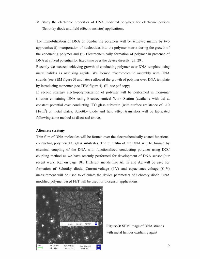
Recently we succeed achieving growth of conducting polymer over DNA template using
metal halides as oxidizing agents. We formed macromolecule assembly with DNA
strands (see SEM figure 3) and later r allowed the growth of polymer over DNA template
by introducing monomer (see TEM figure 4). (Pl. see pdf copy)
In second strategy electropolymerization of polymer will be performed in monomer
solution containing DNA using Electrochemical Work Station (available with us) at
constant potential over conducting ITO glass substrate (with surface resistance of ~10
Ω/cm2) or metal plates. Schottky diode and field effect transistors will be fabricated
following same method as discussed above.
Alternate strategy
Thin film of DNA molecules will be formed over the electrochemically coated functional
conducting polymer/ITO glass substrates. The thin film of the DNA will be formed by
chemical coupling of the DNA with functionalized conducting polymer using DCC
coupling method as we have recently performed for development of DNA sensor [our
recent work: Ref on page 18]. Different metals like Al, Ti and Ag will be used for
formation of Schottky diode. Current-voltage (I-V) and capacitance-voltage (C-V)
measurement will be used to calculate the device parameters of Schottky diode. DNA
modified polymer based FET will be used for biosensor applications.
Figure-3: SEM image of DNA strands
with metal halides oxidizing agent

10
Figure-4: TEM image of DNA coupled with polyindole conducting polymer formed using
our novel technique (as shown in figure3)
References
[1] Hihath J, Bruot C, Tao NJ “Electron-Phonon Interactions in Single Octane dithiol
Molecular Junctions” ACS Nano 4, Pages: 3823-3830,2010.
[2] S. Kohler and P. Hänggi, Nat. Nanotechnol. 2, 675, 2007.
[3] S. Sönmezoğlu, S. Şenkul, R. Taş, G. Çankaya, and M. Can, Thin Solid Films, 518,
4375, 2010.
[4] C. A. Mirkin, R. L. Letsinger, R. C. Mucic, and J. J. Storhoff, Nature London, 382,
607,1996.
[5] C. J. Murphy, M. R. Arkin, Y. Jenkins, N. D. Ghatlia, S. H. Bossmann, N. J. Turro,
and J. K. Barton, Science, 262, 1025, 1993.
[6] Y. Okahata, T. Kobayashi, K. Tanaka, and M. Shimomura, J. Am. Chem. Soc., 120,
6165,1998.
[7] Y. Maeda, H. Tabata, and T. Kawai, Appl. Phys. Lett., 79, 1181, 2001.
[8] O. Gullu, M. Cankaya, O. Baris, A. Turut, Appl. Phys. Lett., 92, 212106, 2008.

11
[9] O. Gullu, M. Cankaya, O. Baris, M. Biber, H. Ozdemir, M. Gulluce, A. Turut, Appl.
Surf. Sci., 254, 5175,2008 (b) O. Gullu, M. Cankaya, O. Baris, A. Turut, Microelectron.
Eng., 85, 2250, 2008.
[10] Giuseppe Maruccio, Paolo Visconti, Valentina Arima, Stefano D’Amico, Adriana
Biasco, Eliana D’Amone, Roberto Cingolani, and Ross Rinaldi, Nano Lett., 3, 479483, 2003
[11] Samuel M.Khamis,RobertR.Johnson, Zhengtang Luo, A.T.CharlieJohnson, J. Phys.
Chem. of Solids, 71, 476, 2010.
[12] Y.S. Jo, Y. Lee, Y. Roh, Mater. Sci. Eng. C, 23, 841, 2003.
[13] P. J. de Pablo, F. Moreno-Herrero, J. Colchero, J. Gomez Herrero, P. Herrero, A. M.
Baro, P. Ordejon, J. M. Soler, and E. Artacho, Phys. Rev. Lett., 85, 4992, 2000.
[14] A. J. Storm, J. van Noort, S. de Vries, and C. Dekker, Appl. Phys. Lett., 79, 3881, 2001.
[15] Y. Zhang, R. H. Austin, J. Kraeft, E. C. Cox, and N. P. Ong, Phys. Rev. Lett., 89,
198102, 2002.
[16] J. S. Hwang, K. J. Kong, D. Ahn, G. S. Lee, D. J. Ahn, and S. W. Hwang, Appl.
Phys. Lett., 81, 1134, 2002.
[17] H. Watanabe, C. Manabe, T. Shigematsu, K. Shimotani, and M. Shimizu, Appl.
Phys. Lett., 79, 2462, 2001.
[18] P. Tran, B. Alavi, and G. Grüner, Phys. Rev. Lett., 85, 1564, 2000.
[19] B. Hartzell, B. McCord, D. Asare, H. Chen, J. J. Heremans, and V. Soghomonian,
Appl. Phys. Lett., 82, 4800, 2003.
[20] K. P. Kamloth, Chem. Rev.,108, 367, 2008
[21] R. H. Friend, Pure Appl. Chem., 73 (3) 425, 2001.
[22] A. K Singh, R. Prakash, A. D. D. Dwivedi and P. Chakrabarti, “IEEE Electron
Device Letter, 29, 571, 2008.
[23] A Tsumura, H. Koezuka and T Ando Appl. Phys. Lett., 49, 18, 1986.
[24] Su X D. , Biochem Biophys Res Commun, , 290 (3), 962, 2000
[25] Wang J, Jiang M., Langmuir, 16(5), 2269, 2000.
[26] Gibbs J M, Park S J, Anderson D R, Watson K J, Mirkin C A, Nguyen S B T., J Am
Chem Soc, 127(4), 1170, 2005.
[27] Lassalle N, Mailley P, Vieil E, Livache T, Roget A, Correia J P, Abrantes L M., J
Electroanal Chem, 509(1), 48, 2001.
[28] Wang J, Jiang M, Fortes A, Mukherjee B., Anal Chim Acta, 402 (1-2), 7, 1999.
[29] Jiang M, Wang J. Recognition and detection of oligonucleotides in the presence of
chromosomal DNA based on entrapment within conducting polymer networks. J
Electroanal Chem, 500(1-2), 584, 2001.

12
[30] Cha J, Han J I, Choi Y, Yoon D S, Oh K W, Lim G., 18(10), 1241, 2003.
[31] Minehan D S, Marx K A, Tripathy S K., 27(3), 777, 1994.
[32] Thompson L A, Kowalik J, Josowicz M, Janata J., J. Am. Chem. Soc, 125(2), 324, 2003.
[33] A. Dawn and Arun K. Nandi, J. Phys. Chem. B, 110, 18291, 2006.
[34] A. Dawn, A. K. Nandi, Macromol. Biosci., 5, 441, 2005.

13
Timelines: (Please provide quantifiable outputs)
Period of study
Achievable targets
0-6 Months
Recruitment of JRF, Purchase of Chemicals and Literature search Start of basic work like design of electrodes, devices and electronic properties of DNA.
7-12 Months Study of electronic properties of DNA and charge conduction mechanism.
13-24 Months
Study of electronic properties of DNA modified with conducting polymers like polyaniline and polyindole and study of charge conduction mechanism at DNA/metal interface and conducting polymers/DNA interfaces.
25-30Months Study of Schottky diodes and field effect transistors based on DNA 31-36 Months
Study of Schottky diodes and field effect transistors based on DNA modified with conducting polymers like polyaniline and polyindole.
20. Name and address of 5 experts in the field
S.No
Name Designation Address
1. Prof. P.C. Pandey
Professor Department of Applied Chemistry Institute of Technology, BHU, Varanasi-05 Email: [email protected] Alternate: [email protected]
2. Dr. C.P. Sharma
Scientist Sree Chitra Tirunal Institute for Medical Sciences & Technology Thiruvananthapuram - 695 011, Kerala, India Email: [email protected]
3. Prof. A.C. Pandey
Professor Nanotechnology Application Centre, University of Allahabad, Allahabad-211 002 Email: [email protected] Alternate: [email protected]
4 Prof. Alok Dhavan
Director Institute of Life Sciences School of Science and Technology Ahmedabad University, 16/1 Vikram Sarabhai Marg, Opp. IIM, Vastrapur, Ahmedabad-380015 Email: [email protected] Alternate: [email protected]
5. Dr. Ashok Pandey
Scientist F And Head
National Institute for Interdisciplinary Science and Technology, CSIR Lab Industrial Estate P.O. Pappanamcode Thiruvananthapuram, Kerala 695 019 Email: [email protected]

14
PART IV: BUDGET PARTICULARS Budget (In Rupees) A. Non-Recurring (e.g. equipments, accessories, etc.)
S. No.
Item Year 1 Year 2 Year 3 Total
1. 2. 3 4..
Up-gradation of existing Potentiostat for FRA (frequency response analyser) mHz to MHz Thermal vapour deposition unit Spin coating Unit Electrical mini probe for conductivity measurements
6,00,000 8,00,000 4,00,000 5,00,000
- - 6,00,000 8,00,000 4,00,000 5,00,000
Sub-Total (A) Rs. 23,00,000 B. Recurring B.1 Manpower (See guidelines at Annexure-III)
S. No.
Position No.
Consolidated Emolument
Year 1 Year 2 Year 3 Total Rs.
1 JRF
Rs. 4,32,000 @12,000/month
1,44,000
1,44,000
1,44,000
4,32,000
Sub-Total (B.1) = Rs. 4,32,000 B.2 Consumables
S. No.
Item
Year 1 Year 2 Year 3 Total
1. 2. 3.
Cell attachment and screen printed electrodes for electrochemical work with adaptor and instruments. DNA and biomolecules and other Monomers and reagents for polymerization
2,00,000 50,000 25,000
- 50,000 25,000
- 50,000 25,000
2,00,000 1,50,000 75,000
Sub-Total (B.2) = Rs. 4,25,000
Other items Consolidated Emolument
Year 1 Year 2 Year 3 Total
B.3 Travel
Rs. 75,000 25,000 25,000 25,000 75,000
B.4 Contingency
Rs. 1,50,000 50,000 50,000 50,000 1,50,000
B.5 Overhead (If applicable)
@15% or as per rule
- - -
Sub-total of B (B.1+B.2+B.3+B.4+B.5)
Rs. 10,82,000 + 15% Over Head1,62,300
6,56,300 2,94,000 2,94,000 12,44,300 Including Over Head
Grand Total (A + B)
Rs.23,32,000 29,56,300 2,94,000 2,94,000 Rs.35,44,300 Including Over head
Note : Please give justification for each head and sub-head separately mentioned in the above table.
Financial Year : April – March Justification: Pl. see enclosure-2

15
PART V: EXISTING FACILITIES Resources and additional information
1. Laboratory:
a. Manpower: Ph.D. students: 8 working on Institute or CSIR fellowships Project Student: One project fellow in DST project and One in NALCO Industrial Project
b. Equipments:
* Required up-gradation and computer interface Apart from this we have XRD, SEM, AFM facilities available in the School for structural and morphological characterizations related to this project work.
2. Other resources such as clinical material, animal house facility, glass house. Experimental garden, pilot plant facility etc.
All the above facilities are available in the University. Not required in this project
S.No. Name of equipment Make 1. FET characterization setup as dual channel source
meter Keithley-Model 2612A
2. I-V characterization set up (Current source meter with nano voltmeter) without mini-probe
Keithley- Model 6220 and 2182A
3. Electrochemical work station CH Instrument 4. Electrochemical work station with Quartz Crystal
Microbalance Autolab
5. UV-vis Abs Spectrophotometer Perkin Elmer 6. Thermal Analyser
DSC and TGA/DTA Mettler-Toledo 832
7. Dual Channel Source Meter 8. FT-IR Thermo 9. Synthesis and basic characterization facilities
related to conducting polymers and sensors -

16
PART VII: PROFORMA FOR BIOGRAPHICAL SKETCH OF
INVESTIGATORS Provide the following information for the key personnel in the order listed on PART II.
Follow this format for each person. DO NOT EXCEED THREE PAGES
Name : .......……………Dr. Rajiv Prakash.......................................................................
Designation :…………..Professor.....................................................................
Department/Institute/University:
School of Materials Science and Technology, ……….………. Institute of Technology, Banaras Hindu University, Varanasi
Phone and Fax: +91-542-2368707 and 2307047 E-mail: [email protected] Alternate: [email protected]
Date of Birth : ..01-07-1971...... Sex (M/F) ......M................... SC/ST : ....No............
Education (Post-Graduation onwards & Professional Career)
Sl No. Institution Place
Degree Awarded
Year Field of Study
1. Banaras Hindu University, Varanasi
B.Sc. 1992 Physics, chemistry, Mathematics and English
2. Banaras Hindu University, Varanasi
M.Sc. 1994 Chemistry (Specialization in Organic Chemistry)
3. Institute of Technology, Banaras Hindu University, Varanasi
M.Tech. 1996 Materials Science and Technology
4. Chemistry, Banaras Hindu University, Varanasi Working Place: Chemical Physics Group, TIFR, Bombay
Ph.D. 2000 Organic conducting polymers and their technological applications
Position and Honors Position and Employment (Starting with the most recent employment)
Sl No. Institution Place
Position From (Date) To (date)
1. Analytical Division “Indian Institute of Toxicology Reserach”, CSIR, Lucknow
Scientist Gr IV (i) May 1997 July 2004
2. Chemistry, Banaras Hindu University, Varanasi
Assistant Professor July 2004 Sept. 2004
3. Institute of Technology, Banaras Hindu University, Varanasi
Associate Professor Sept. 2004 Sept 2010
4. Institute of Technology, Banaras Hindu University, Varanasi
Professor Sept. 2010 Till date

17
Honors/Awards (1) MRSI Medal 2010 (Materials Research Soc., India)
(2) Young Engineers Awards-2005 of Indian National Academy of Engineering
(3) Young Scientist Award-2003 of U.P. Council of Science and Technology.
(under Department of Science and Technology)
(4) Visiting Scientist (under DAAD Scholarship) at Johannes Gutenberg University,
Mainz, Germany (2002-2003)
(5) Editor in Journals Editorial Board:
1. Member Editorial Board of Journal of Sensor Technology, Scientific Research Publishing,
USA http://www.scirp.org/journal/jst/ E-ISSN: 2161-1238 P-ISSN Print: 2161-122X
2. Member Editorial Board of Biosensors Journal, Ashdin Publishing, UK. <http://mts.ashdin.com/>
http://www.ashdin.com/journals/bj/Rajiv_Prakash.aspx. E-ISSN: 2090-4967; P-ISSN: 2090-4959
3. Editor and Member, Board of Academic matters and Publication-NST Consortium Journal
Nano Trends <http://www.stmjournals.com> P-ISSN 0973-418X
4. Editor and Member, Board of Academic Matters and Publication-STM Journal Consortium
J NanoScience, Nanoengineering & Applications <http://www.stmjournals.com>
5. Member, Advisory Editorial Board of International Journal of Research, India
<http://www.ijrimsec.com> P-ISSN-0976-8211
Member Advisory committee of TIFAC for India Technology Vision Plan 2035 on Materials and Processing
Professional Experience and Training relevant to the Project PI is working in the area of Sensors and Biosensor from 1997 (as a Scientist in IITR, Lucknow) and started bio-electronics during his stay in University of Mainz, Germany. At present PI is working in the area of Sensors and Biosensors under collaboration with Biochemical and Biomedical Engineering departments of the IT, BHU and extensively involve in Organic Electronics and Bio-electronics areas with collaboration of Electronic department of the IT, BHU as well as with Life Science Group of Kyushu Institute of Technology, Kitakyushu, Japan (Under DST-JSPS). B. Publications (Numbers only) 73 (International)
Books : ....01............. Research Papers, Reports: ..73..............General articles…………....
Patents : ...15.............Others (Please specify) :.....Indian 05..............................................
Guiding Project /Ph.D. Students: M. Tech. Project: 23 (including 1 working at present)
Ph.D.: 05 Submitted/Awarded and 8 working at present
[Including co-supervisor for 1 student in Dept. Electronics, IT, BHU]
18
Selected peer-reviewed publications (Ten best publications in chronological order) 1. Electronic Properties and Photoresponse of Polycarbazole-Multiwalled Carbon
Nanotube Nanocomposite/Aluminum Schottky Diode Arun Kumar Singh, P. Chakrabarti and Rajiv Prakash IEEE Electron Device Letters, 32, 5 (2011) 593-595.
2. Organic Schottky Diode based on Conducting Polymer-Nanoclay Composite Arun Kumar Singh and Rajiv Prakash RSC Adv. (In press, 2012) DOI:10.1039/C2RA20206A.
3. Methanol Derived Large Scale Chemical Synthesis of Brightly Fluorescent Graphene Vyom Parashar, Kaushal Kumar, Rajiv Prakash, Shiv K Pandey, Avinash C Pandey, Journal of Materials Chemistry, 21 (2011) 6506-6509.
4. Novel Synthesis of Polycarbazole–Gold Nanocomposite Bhavana Gupta, Leela Joshi, Rajiv Prakash Macromolecular Chemistry and Physics, 212 (2011) 1692-1699
5. Nano Structured Nickel Oxide based DNA Biosensor for Detection of Visceral Leishmaniasis (Kala-azar)
Swati Mohan, Pankaj Srivastava, S. N. Maheshwari, Shyam Sundar, Rajiv Prakash, Analyst, 136 (2011) 2845-2851 6. Reactive Compatibilization of Polycarbonate (PC) and Poly (methyl
methacrylate) (PMMA) in the Presence of a Novel Transesterification Catalyst SnCl2.2H2O. Ahilesh Kumar Singh, Rajiv Prakash, Dhananjai Pandey, Journal of Physical Chemistry B, 115 (2011) 1601-1607
7. Synthesis of Functionalized Conducting Polymer “Polyanthranilic Acid” Using
Various Oxidizing Agents and Formation of Composites with PVC Bhavana Gupta and Rajiv Prakash, Polymers for Advanced Technologies, 22 (2011) 1982–1988. 8. Structural, Thermal, and Fluorescence Properties of Eu(DBM)3Phenx Complex
Doped in PMMA A. Singh, Sunil Singh, Hirdyesh Mishra, Rajiv Prakash, S. B. Rai
J Physical Chemistry B, 114 (2010) 13042–13051. 9. A Label-Free Genosensor for BRCA1 Related Sequence based on Impedance
Spectroscopy. Swati Mohan, Preeti Nigam, Subir Kundu, Rajiv Prakash, Analyst, 135(2010) 2887-2893.
10. Novel Conducting Polymer Functionalized with Metal-Cyclam Complex and its Sensor Application: Development of Azidothymidine Drug Sensor. Swati Mohan and Rajiv Prakash, Talanta, 81 (2010) 449–454.

19
List maximum of five recent publications relevant to the proposed area of work. 1. Synthesis of Nano Ground Nutshell-like Polyindole by Supramolecular
Assembled Salts of ss-DNA Assisted Chloroauric Acid Ashish Kumar and Rajiv Prakash Chemical Physics Letters, 511 (2011) 77–81
2. A label-free genosensor for BRCA1 related sequence based on impedance spectroscopy. Swati Mohan, Preeti Nigam, Subir Kundu, Rajiv Prakash, Analyst, 135(2010) 2887-2893.
3. Controlled Drug Release Characteristics and Enhanced Antibacterial Effect of Graphene Nanosheets Containing Gentamicin Sulphate H Pandey, V Parashar, R Parashar, Rajiv Prakash, P W Ramteke, A C Pandey, Nanoscale (2011) doi. 10.1039/C1NR10661A 4. Nano Structured Nickel Oxide based DNA Biosensor for Detection of Visceral Leishmaniasis (Kala-azar) Swati Mohan, Pankaj Srivastava, S. N. Maheshwari, Shyam Sundar, Rajiv Prakash, Analyst, 136 (2011) 2845-2851 5. Electronic Properties and Photoresponse of Polycarbazole-Multiwalled Carbon Nanotube Nanocomposite/Aluminum Schottky Diode Arun Kumar Singh, P. Chakrabarti and Rajiv Prakash IEEE Electron Device Letters, 32, 5 (2011) 593-595 Research Support
Ongoing Research Projects
Sl No.
Title of Project Funding Agency
Amount Date of sanction and Duration
1. “Development of DNA based biosensor and application for detection of Listeria Monocytogenes”
DST and Inductry project
~28 Lakhs (Industry 3 lakhs)
Ref: IDP/Sen/137/08 Dated 14.6.2010
2. “Development of Azidothymidine (Anti HIV drug) and its Reactive Phase-I Metabolites Electrochemical Sensor based on Low Cost Screen Printed Electrodes”
DST ~30 Lakhs Fund Received Dec 2011
3. “Morphology Control of Organic Materials for Nanobioelectronics Devices”
JSPS-DST (Indo-Japan)
~ 5 Lakhs 2011-2013
4. “Electrochemical sensors for heavy metal ions (Zn, Cu, Ni) in Industrial waste water”
NLC NALCO
~20,000 USD 2012-13

20
Completed Research Projects (State only major projects of last 3 years)
Sl No.
Title of Project Funding Agency Amount Date of completion
1. “Development of Optically Active Polymers for Data Storage Applications” (Co-PI)
DIT and Industry (MBIL) project
~200 Lakhs (Industry 80 laksh)
July 2010
2. “Development of Lead and Copper Screen Printed Sensors”.
CSIR ~8 Lakhs
June 2009
3. “Studies of the Effect of High Energy Irradiation on Conducting Polymers”
IUAC-UGC
~4 Lakhs
Dec. 2009
Place : IT, BHU Signature of Investigator Date :

21
Enclosure-1 Project Summary: Recent studies on the electrical conduction of DNA molecules reveal that they may act as
either semiconductor with nanosize dimensions or non-semiconducting materials. The
actual magnitude of DNA conductivity and its physical mechanism is still under debate,
since experiments indicate that this biomolecule can behave as an insulator, a wide
bandgap semiconductor, a good conductor, or even a proximity-induced superconductor.
More investigations are required to settle the existing controversies about the electrical
conductivity behaviour of the DNA molecules. If they are like semiconductors, they may
find very interesting applications not only in use as such semiconducting materials for
electronic devices but also improving the major limitations of organic semiconductors
like low mobility and stability. The field of DNA electronics is highly interdisciplinary,
interfacing physics, biology, chemistry, computer science, engineering and so on.
Recently efforts are made in developing DNA-organic polymers or organic conductors
hybrid materials for various applications. It is believed that organic conducting polymers
may offer an efficient way for DNA grafting (due to having pH dependent charges) and
may be able to modulate long range charge transport through strong interactions with
attached DNA molecules. Most of the workers have studied only structural,
morphological, and chemical kinetics of DNA modified organic conducting polymers,
only a few papers are reported for electronic properties of DNA modified organic
conducting polymers. The main thrust is on the use of DNA-organic molecules
interaction and formation of hybrid materials for much smaller, faster and more energy
efficient semiconductor-based electronic devices.
In this project we propose to address a few key questions like the actual magnitude of
DNA conductivity and its physical mechanism, understanding of its electronic properties
and interfacial electronic phenomena at DNA/metal interface. Further we are proposing
DNA-organic polymer hybrid material formation and study of polymers/DNA hybrid
material for electronic devices. These studies will not only be important from scientific
point of view but technological also for the development of new type of materials for
semiconducting devices as well as for improving the performance of organic devices. We
have proposed I-V and C-V characteristics of DNA and DNA-conducting polymer hybrid
materials to develop DNA or DNA modified polymers based electronic devices like
Schottky diode and field effect transistors in this project. DNA and DNA modified
polymer based Schottky diode and field effect transistors may be further explored for

22
various technological applications. Our preliminary work in this direction has given
encouraging results (Rajiv Prakash et al., Chemical Physics Letters, 511 (2011) 77–81)
and we successfully polymerized conducting polymer over DNA template and formed
polymer-DNA hybrid material.

23
Enclosure-2 Justification for budget: Instruments: C-V measurement is an important parameter for study of the electronic properties of semiconducting materials. Our proposed work for study of electronic properties and charge transfer mechanism in DNA and DNA modified with conducting polymer will be mainly based on I-V and C-V measurements and further various calculations and device parameters (Diode and FET devices) will be calculated using I-V and C-V plots. We have Keithley instruments for the study of I-V but I do not have any instrument for C-V analysis. New instrument is costing more than 15 lakhs but on investment of 5 lakhs for up-gradation of our existing potentiostat will solve our purpose for impedance analysis. Further for conductivity measurements we need mini probe which is not available in our lab. It will be attached with our existing Keithley instruments. For device fabrication we need Thermal Vapour Deposition Unit and Spin Coating Unit. Thermal vapour deposition unit will be used for fabrication of devices as shown in Fig.1 and spin coating unit will be used for coating of chemicals and biochemicals over devices as shown in Fig.2 in this proposal. These instruments are frequently required and we do not have this facility in our School (so far we are using from Electronics Department). Man power Man power is required for proper implementation of the proposed work. Student will be trained for various synthesis techniques and in electronic devices fabrication. A JRF will be benefited a lots with this type of training and also work in novel area of bio-electronics. Consumables: The major part under this head is electrochemical cell attachment and electrodes suitable for this work. Screen printed electrode with adaptor will be purchase for this work. It is required for electrochemical synthesis of conducting polymer and coupling of the DNA with conducting polymer followed by characterization using a disposable screen printed electrodes. The other consumable items i.e. monomers of the conducting polymers, various reagents required for coupling, DNA will be purchased from this head. These chemicals are very costly due to requirement of their high grades. Apart from this consumables for device fabrications and high purity metals will be purchased out of this head. Contingency: It will be used for development of devices and electrodes. Design of the solid state electrodes and device electrodes will be costly. It will require Teflon, peek, PVC and SiO2 materials for construction of electrodes. These materials will be purchased first in small quantity, which will be much costly.

24
Fabrication required in the project for the electrodes, testing cell and incubation/drying chambers, which will be carried out from this head. Travel Grant: This grant will be used for attending the conferences and interactions with other labs related to the project. It will also be used for inviting eminent scientists and academicians working in related area to give invited talk in our School.

25
dk’kh fgUnw fo’ofo|ky;
BANARAS HINDU UNIVERSITY (laln ds i=kad la[;k 225 ds kjk 1916 esa LFkkfir) (Established by Parliament Notification No. 225 of 1916)
PART VI: DECLARATION/CERTIFICATION It is certified that a) the research work proposed in the scheme/project does not in any way duplicate the work already done or being carried out elsewhere on the subject. b) the same project proposal has not been submitted to any other agency for financial support. c) the emoluments for the manpower proposed are those admissible to persons of corresponding status employed in the institute/university or as per the Ministry of Science & Technology guidelines (Annexure-III) d) necessary provision for the scheme/project will be made in the Institute/University/State budget in anticipation of the sanction of the scheme/project. e) if the project involves the utilizationof genetically engineered organisms, we agree to submit an application through our Institutional Biosafety Committee. We also declare that while conducting experiments, the Biosafety Guidelines of the Department of Biotechnology would be followed in toto. f) if the project involves field trials/experiments/exchange of specimens, etc. we will ensure that ethical clearances would be taken from concerned ethical Committees/ Competent authorities and the same would be conveyed to the Department of Biotechnology before implementing the project. g) it is agreed that any research outcome or intellectual property right(s) on the invention(s) arising out of the project shall be taken in accordance with the instructions issued with the approval of the Ministry of Finance, Department of Expenditure, as contained in Annexure-V. h) we agree to accept the terms and conditions as enclosed in Annexure-IV. The same is signed and enclosed. i) the institute/university agrees that the equipment, other basic facilities and such other administrative facilities as per terms and conditions of the grant will be extended to investigator(s) throughout the duration of the project. j) the Institute assumes to undertake the financial and other management responsibilities of the project.
Signature of Principal Investigator Signature of Executive Authority Date : of Institute/University with seal Date :