molecular electronics: beyond coulomb blockadephys533/notes/lecture29.pdf · molecular electronics:...
TRANSCRIPT
1
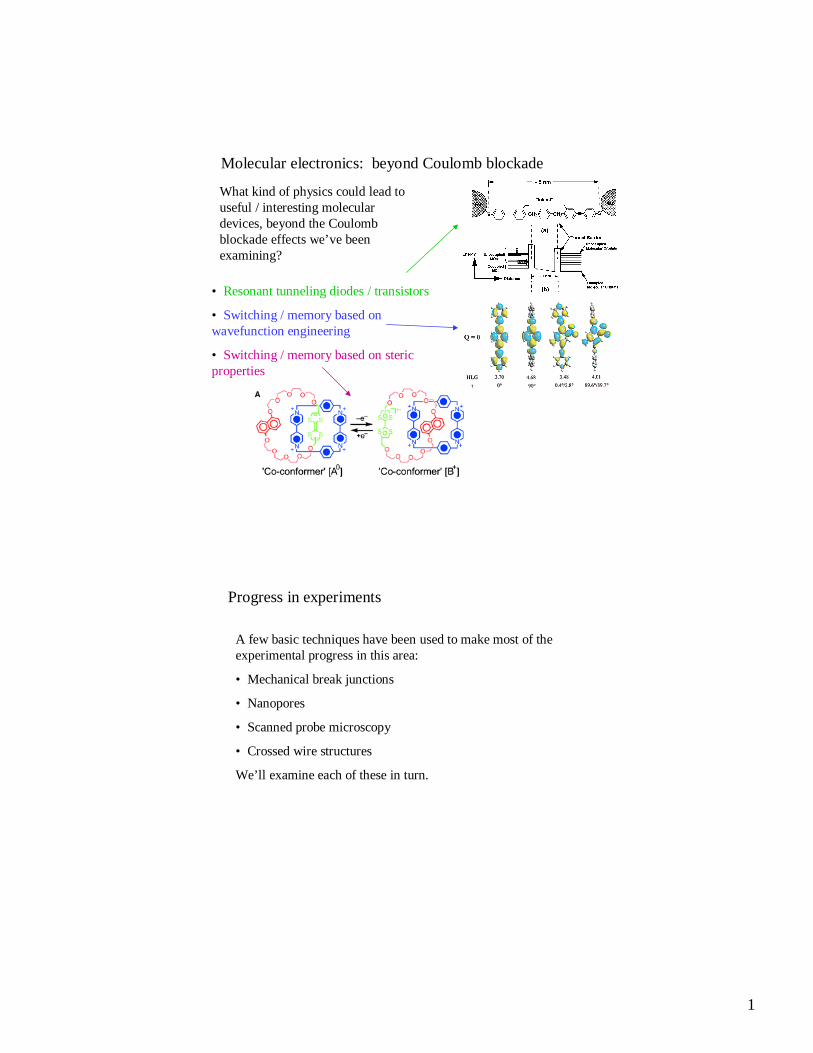
Molecular electronics: beyond Coulomb blockade
• Resonant tunneling diodes / transistors
• Switching / memory based on wavefunction engineering
• Switching / memory based on steric properties
What kind of physics could lead to useful / interesting molecular devices, beyond the Coulomb blockade effects we’ve been examining?
Progress in experiments
A few basic techniques have been used to make most of the experimental progress in this area:
• Mechanical break junctions
• Nanopores
• Scanned probe microscopy
• Crossed wire structures
We’ll examine each of these in turn.

2
Mechanical break junctions
Basic idea:Mechanical advantage: lateral motion from bending can be ~ 1000x smaller than vertical motion.
Breaking can be done in UHV to avoid contamination.
Bare metal tunneling current allows calibration of position.
Images from van Wees group, Netherlands
Zhou et al., APL 67, 1160 (1995).
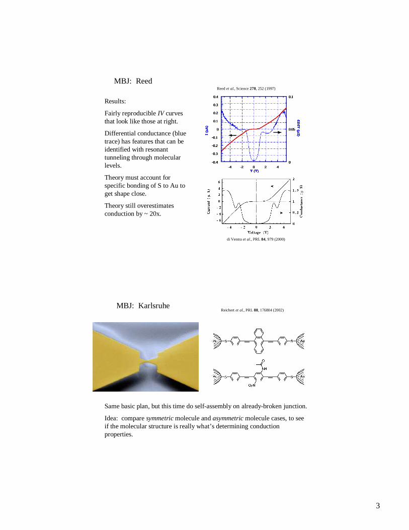
MBJ: Reed
Reed et al., Science 278, 252 (1997)Start with unbroken wire, precoated with self-assembled monolayer (SAM) of interesting molecule.
Break in UHV and allow molecules to rearrange.
Bring junction back together for measurements, knowing what piezo voltage corresponds to the correct interelectrode spacing.
3
MBJ: Reed
Results:
Fairly reproducible IV curves that look like those at right.
Differential conductance (blue trace) has features that can be identified with resonant tunneling through molecular levels.
Theory must account for specific bonding of S to Au to get shape close.
Theory still overestimates conduction by ~ 20x.
Reed et al., Science 278, 252 (1997)
di Ventraet al., PRL 84, 979 (2000)
MBJ: KarlsruheReichert et al., PRL 88, 176804 (2002)
Same basic plan, but this time do self-assembly on already-broken junction.
Idea: compare symmetric molecule and asymmetric molecule cases, to see if the molecular structure is really what’s determining conduction properties.
4
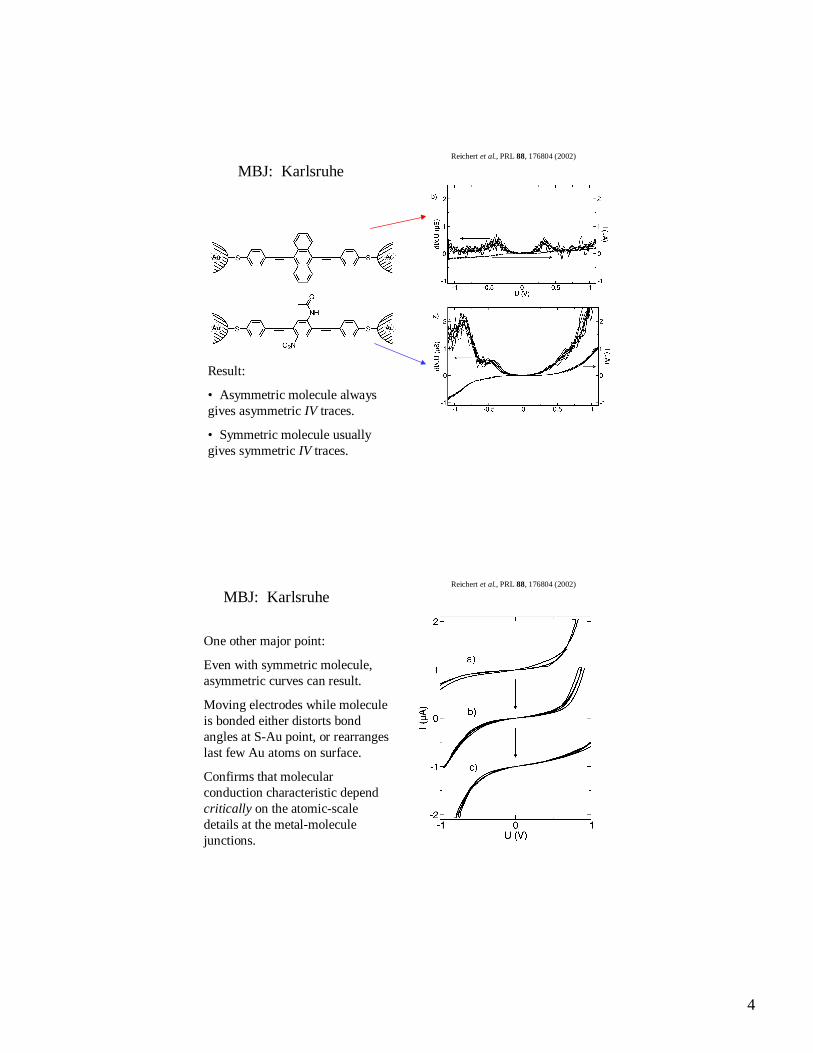
MBJ: KarlsruheReichert et al., PRL 88, 176804 (2002)
Result:
• Asymmetric molecule always gives asymmetric IV traces.
• Symmetric molecule usually gives symmetric IV traces.
MBJ: KarlsruheReichert et al., PRL 88, 176804 (2002)
One other major point:
Even with symmetric molecule, asymmetric curves can result.
Moving electrodes while molecule is bonded either distorts bond angles at S-Au point, or rearranges last few Au atoms on surface.
Confirms that molecular conduction characteristic depend critically on the atomic-scale details at the metal-molecule junctions.

5
MBJ: Crossed wiresKushmericket al., PRL 89, 086802 (2002)
Same point can be made in an even simpler crossed-wire geometry at room temperature.
MBJ: Crossed wires and vibrations
Kushmericket al., Nano Lett. 4, 639 (2004)
• Junctions made this way are stable enough to allow measurements of d2I/dV2.
• Inelastic electron tunneling features make sense.

6
MBJ: Gating
• Possible (though hard!) to make mechanical break junctions in gate-able configurations!
• Potentially very important technique.
Champagne et al., cond-mat/0409134
MBJ summary
• Highly productive research technique for examining single molecules.
• Shows that single molecule conduction is possible, though generally poor.
• Single molecule conduction depends crucially on atomic-scale details of bonding and metal surfaces.
• Gating is possible under certain circumstances.
Endemic problems with technique:
• Mechanical stability essential.
• Very difficult to do temperature sweeps - everything moves due to differential contraction. This is a problem b/c standard way ofdeducing conduction mechanisms uses G(V,T).

7
Nanopores Images from Reed group, Yale
Not a single molecule technique - more like ~ 1000 in parallel.
Originally developed to study ~ 10-30 nm diameter metal junctions.
NanoporesImages from Reed group, Yale
Requires self-assembly followed by evaporation of top electrode.
Noone knows what interface looks like.
Yield very very low (~ 1-2 %).
8
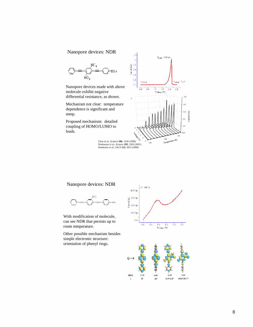
Nanopore devices: NDR
Chen et al., Science 286, 1550 (1999)Donhauser et al., Science 293, 2303 (2001)Seminario et al., JACS 122, 3015 (2000)
Nanopore devices made with above molecule exhibit negative differential resistance, as shown.
Mechanism not clear: temperature dependence is significant and steep.
Proposed mechanism: detailed coupling of HOMO/LUMO to leads.
Nanopore devices: NDR
With modification of molecule, can see NDR that persists up to room temperature.
Other possible mechanism besides simple electronic structure: orientation of phenyl rings.

9
Nanopore devices: memory Reed et al., APL 78, 3735 (2001).
Hysteretic IV curves.
Initial ramp up: “high” conductance state.
Ramp back down: “low” conductance state, until reset.
Like NDR, effect is strongly temperature dependent.
Requires very large electric fields to actuate….
Nanopore devices: memory
Can clearly use this kind of hysteretic IV curve as a memory!
Again, potential mechanisms are either wavefunction oriented (shape of electron distribution in HOMO and LUMO) or steric (reorientation of side groups).

10
Nanopore devices: simple tunneling + vibrationsWang et al., PRB 68, 035416 (2003)
Wang et al., Nano Lett. 4, 643 (2004)
• Recent nanopore papers on very “boring” molecules show nice results.
• Conduction really is via tunneling.
• Inelastic features make sense.
Scanned probe microscopy: STM
Paul Weiss, PSU
Another means of looking for interesting molecules and testing their (2-terminal) conductive properties is to use scanned probe microscopes.
• Allows highly controlled positioning of electrodes previously decorated with molecules.
• Can obtain I-V curves for single molecules.
• Can quickly examine many molecules

11
Scanned probe microscopy: STM
Downsides:
• Mechanical stability
• Difficult to do T-dep. measurements.
• Interpretation of contacts difficult -tunneling conductance is supposed to be proportional to product of local single-particle density of states of tip and surface.
• As result, tricky to deconvolve topography from electronic properties.
One time it’s not too hard: time-varying behavior
Donhauseret al., Science 292, 2303 (2001).
Scanned probe microscopy: AFM
Cui et al., Science 294, 571 (2001)
Conducting AFM is also a useful tool.
Downside: contact area is typically significantly larger than single molecule.
Upside: can vary contact force and see what happens.
Surprisingly nice result at right: looks like as Au nanoparticle is pressed harder, more and more molecules are in contact in the circuit.
Tricky to reconcile this with the data shown previously demonstrating that contact geometry is huge influence.

12
Nanopore and SPM summary
• Nanopores have produced some impressive results - NDR, memory w/ T-dependent measurements of ~ 1000 molecules in ||.
• Problem is, yields are terrible, and diagnostics on final molecule condition is essentially impossible.
• SPM techniques are much faster, and confirm some of the nanopore work (NDR, switching of conductance states).
• Unfortunately, SPM has its own set of experimental issues.
• Mechanisms behind these properties still argued.
Crossed wire structuresCollier et al., Science 285, 391 (1999)Collier et al., Science 289, 1172 (2000)
On industrial side, HP and UCLA have been working on “crossed wire” structures.
Suffer from same diagnostic concerns as nanopore devices, though much easier to fabricate (larger overlap).
•Molecules have hysteretic IVcurves - may be used for nonvolatile memory.
• Limited to 2-terminal devices without gain, but that’s not so crucial for nonvolatile memory schemes.
13
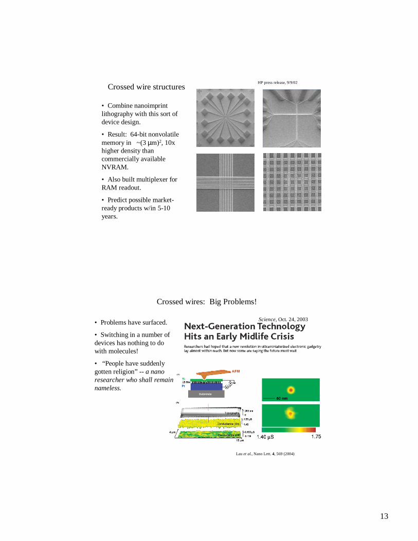
Crossed wire structuresHP press release, 9/9/02
• Combine nanoimprint lithography with this sort of device design.
• Result: 64-bit nonvolatile memory in ~(3 µm)2, 10x higher density than commercially available NVRAM.
• Also built multiplexer for RAM readout.
• Predict possible market-ready products w/in 5-10 years.
Crossed wires: Big Problems!
• Problems have surfaced.
• Switching in a number of devices has nothing to do with molecules!
• “People have suddenly gotten religion” --a nano researcher who shall remain nameless.
Science, Oct. 24, 2003
Lau et al., Nano Lett. 4, 569 (2004)
14
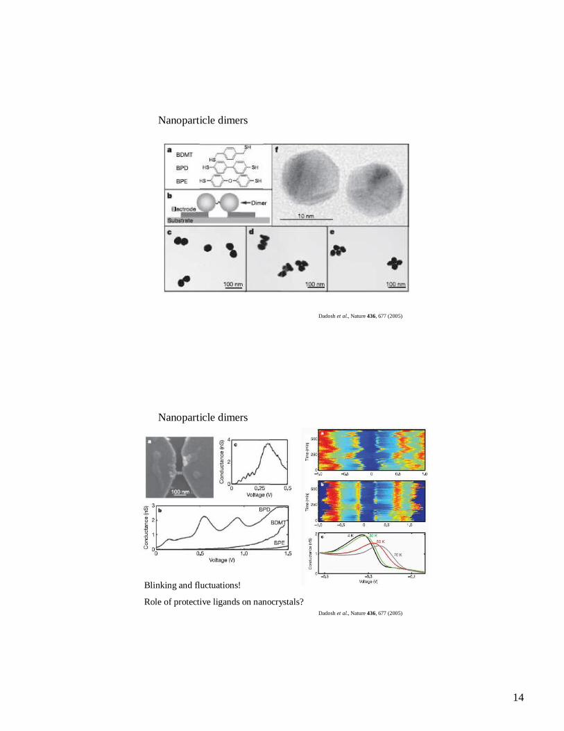
Nanoparticle dimers
Dadoshet al., Nature 436, 677 (2005)
Nanoparticle dimers
Dadoshet al., Nature 436, 677 (2005)
Blinking and fluctuations!
Role of protective ligands on nanocrystals?

15
Nanocell concept
The researchers: Tour (Rice), Reed (Yale), Allara (Penn State), Mallouk (Penn State)
Nanocell concept:
• Self-assemble large number of functionalized nanoparticles + molecules (e.g. NDR and memory molecules) across an array of leads.
• Training + field programming: apply voltage pulses; measure currents; train system to have desired functionality (!).
Nanocell conceptinput terminals
output terminals
• Every device is unique (analogous to detailed wiring of brain).
• Architecture that permits on-the-fly adaptation and training would be inherently robust + defect tolerant.
• A huge departure from standard electronics manufacturing practice!
Molecular Electronics Corp. / Motorola paradigm: self-assembly + software architecture to allow training of circuits.

16
Summary and prospects
• Several research tools exist for trying to examine molecular conduction beyond Coulomb blockade.
• Basic qualitative features involving resonant tunneling through levels are understood.
• Details (contacts, quantitative results with predictive power) are still lacking.
• Basic physics responsible for certain interesting properties (NDR, switching) still under debate.
• We’re a long way from practical molecular electronic devices, though applications in niche markets may be on the horizon.
• A fascinating field in which to be working!
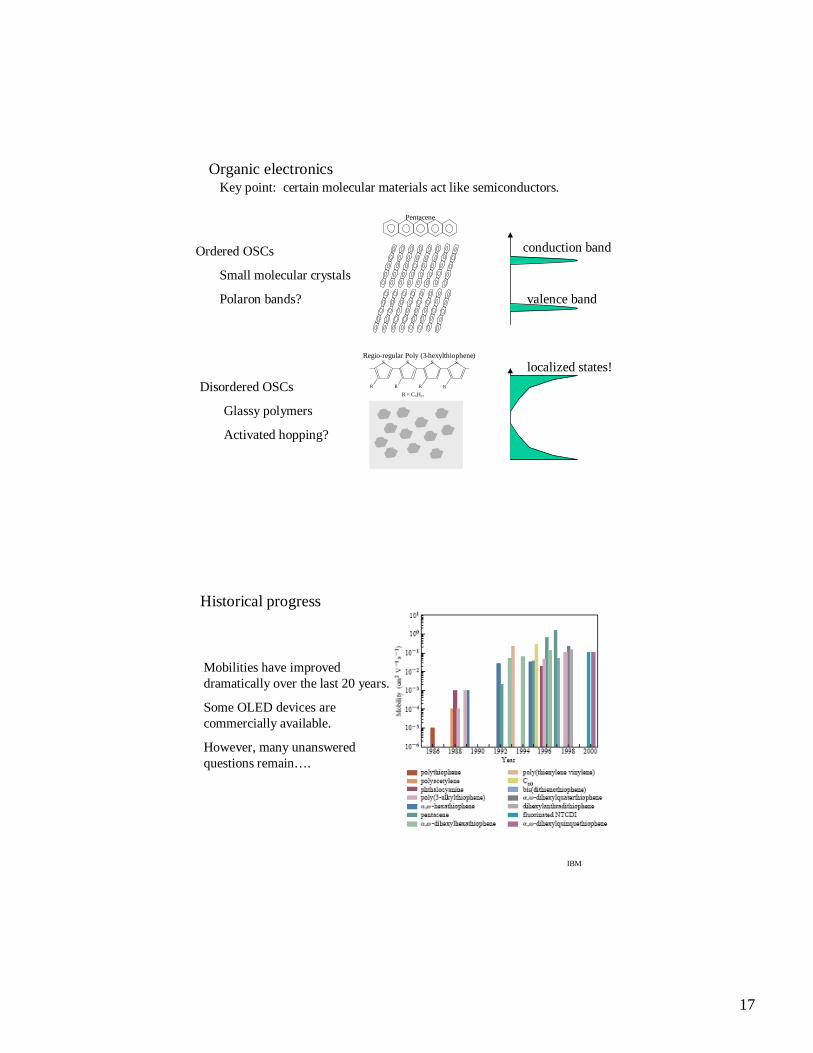
Organic electronics
A thriving research (and commercial !) field already exists using molecular materials.
Organic LEDs Organic FETs
IBM
17
Organic electronics
Pentacene
S S S S
R
R = C6H13
R R R
Regio-regular Poly (3-hexylthiophene)
Key point: certain molecular materials act like semiconductors.
Ordered OSCs
Small molecular crystals
Polaron bands?
Disordered OSCs
Glassy polymers
Activated hopping?
conduction band
valence band
localized states!
Historical progress
Mobilities have improved dramatically over the last 20 years.
Some OLED devices are commercially available.
However, many unanswered questions remain….
IBM

18
Unanswered questions
• What are the basic physical parameters of carriers in organic semiconductors? (Effective masses, etc.)
• What is the physics of charge injection at OSC-metal interfaces?
• How does the conduction mechanism evolve from bands to hopping as disorder is increased?
• What are the fundamental limits of OSC performance?
• How important are electronic correlations in these materials?
Next time….
Basics of magnetism and magnetic materials.