modal formulation for diffraction by absorbing photonic
TRANSCRIPT

arX
iv:1
606.
0039
0v1
[ph
ysic
s.op
tics]
24
Nov
201
5
Modal formulation for diffraction by absorbing
photonic crystal slabs
Kokou B. Dossou1,∗, Lindsay C. Botten1, Ara A. Asatryan1,
Bjorn C.P. Sturmberg2, Michael A. Byrne1, Christopher G. Poulton1,
Ross C. McPhedran2, and C. Martijn de Sterke2
1 CUDOS, University of Technology, Sydney, N.S.W. 2007, Australia
2CUDOS and IPOS, School of Physics, University of Sydney, NSW 2006, Australia
∗Corresponding author: [email protected]
A finite element-based modal formulation of diffraction of a plane wave by
an absorbing photonic crystal slab of arbitrary geometry is developed for
photovoltaic applications. The semi-analytic approach allows efficient and
accurate calculation of the absorption of an array with a complex unit cell.
This approach gives direct physical insight into the absorption mechanism in
such structures, which can be used to enhance the absorption. The verification
and validation of this approach is applied to a silicon nanowire array and the
efficiency and accuracy of the method is demonstrated. The method is ideally
suited to studying the manner in which spectral properties (e.g., absorption)
vary with the thickness of the array, and we demonstrate this with efficient
calculations which can identify an optimal geometry. c© 2018 Optical Society
of America
OCIS codes: 050.1960, 290.0290, 350.6050, 160.5293.
1. Introduction
Photonic crystals, which consist of a periodically arranged lattice of dielectric scatterers,
have attracted substantial research interest over the past decade [1]. Most commonly these
structures are used to trap, guide, and otherwise manipulate pulses of light, and have led
to a variety of important applications in modern nanophotonics, including extremely high-Q
electromagnetic cavities [2] and slow-light propagation of electromagnetic pulses [3]. However,
a new and increasingly important application of photonic crystal structures is in the field
of photovoltaics. It has long been known that structured materials can be used to achieve
1

photovoltaic conversion efficiency beyond the Yablonovitch limit [4,5], and indeed researchers
have recently proposed photonic crystals [6, 7] and arrays of dielectric nanowires [8, 9] as
inexpensive ways to create highly efficient absorbers. Recent research in this area has been
driven by advances in nanostructure fabrication [10] concurrent with increased investment
in renewable energy technology (for the latest developments see [11]).
One aspect in which the use of photonic crystals in photovoltaics differs markedly from
their employment in optical nanophotonics is the important role played by material absorp-
tion. For most nanophotonic applications absorption is an undesirable effect which must in
general be minimized and can in many cases be neglected. This is in stark contrast to pho-
tovoltaics, in which the main aim is to exploit the properties of the structure to increase the
overall absorption efficiency.
Modeling of absorbing photonic crystals has thus far been performed using direct numerical
methods such as the Finite-Difference Time-Domain (FDTD) method [8], the Finite Element
Method (FEM) [12] or using the Transfer Matrix method [9]. Although these methods have
produced valuable information about the absorption properties of such structures they do
not allow us to gain direct physical insight into the mechanism of the absorption within
them. Furthermore, these calculations require substantial computational time and resources.
Here we present a rigorous modal formulation of the scattering and absorption of a plane
wave by an array of absorbing nanowires, or, correspondingly, an absorbing photonic crystal
slab (Fig. 1). The approach is a generalization of diffraction by capacitive grids formulated
initially in Refs [13, 14] for perfectly conducting cylinders. In contrast to conventional pho-
tonic crystal calculations the material absorption is taken into account rigorously, using
measured values for the real and the imaginary parts of the refractive indices of the mate-
rials comprising the array. Our formulation can be applied to array elements of arbitrary
composition and cross-section. The semi-analytical nature of this modal approach results in
a method which is quick, accurate, and gives extensive physical insight into the importance
of the various absorption and scattering mechanisms involved in these structures.
The method is based on an expansion in terms of the fundamental eigenmodes of the
structure in each different region. Within the photonic crystal slab the fields are expanded in
terms of Bloch modes, while the fields in free space above and below the slab are expanded
in a basis of plane waves. These expansions are then matched using the continuity of the
tangential components of the fields at the top and the bottom interfaces of the slab to
compute Fresnel interface reflection and transmission matrices.
An important aspect of this approach is that the set of Bloch modes must form a complete
basis. This is not a trivial matter, as even for structures consisting of lossless materials
the eigenvalue problem for the Bloch modes is not formally Hermitian. However, it is well
known from the classical treatment of non-Hermitian eigenvalue problems [15, p. 884] that a
2

complete basis may be obtained by including the Bloch modes of the adjoint problem. Here,
we use the FEM to compute both the Bloch modes and the adjoint Bloch modes. Because
the mode computation may be carried out in two dimensions (2D) like waveguide mode
calculations, this routine is highly efficient. We note that a previous study [16], undertaken
using a different method, failed to locate some of the modes, as is demonstrated in Sec. 3.A;
we emphasis that the algorithm presented here is capable of generating a complete set of
modes. In addition the FEM allows us to compute Bloch modes for arbitrary materials and
cross sections.
We note that this approach differs from earlier formulations [13,14] in which the photonic
crystal had to consist of an array of cylinders with a circular cross-section. With the modes
identified, the transmission through, and reflection from, the slab can be computed using a
generalization of Fresnel reflection and transmission matrices, and the absorption is found
using an energy conservation relation.
The organization of the paper is as follows. The theoretical foundation of the method
is given in Sec. 2 while the numerical verification, validation and characterization of the
absorption properties of a particular silicon nanowire array occurs in Sec. 3. The details
of the mode orthogonality, normalization, completeness as well as energy and reciprocity
relations are given in the appendices.
2. Theoretical description
As mentioned in Sec. 1, we separate the solution of the diffraction problem into three steps,
one involving the consideration of the scattering of plane waves at the top interface and
the introduction of the Fresnel reflection and the transmission matrices for a top interface
(Fig. 1). Next we introduce the Fresnel reflection and transmission matrices for the bottom
interface by considering the reflection of the waveguide modes of the semi-infinite array of
cylinders at the bottom interface. Then the total reflection and transmission through the
slab can be calculated using a Fabry-Perot style of analysis. The approach is based on the
calculation of the Bloch modes and adjoint Bloch modes of an infinite array of cylinders.
Before doing so however, we first provide the field’s plane wave expansions above and below
the photonic crystal slab.
2.A. Plane wave expansion
In a uniform media such as free space, all components of the electromagnetic field of a plane
wave must satisfy the Helmholtz equation
∇2E + k2E = 0, (1)
where k = 2π/λ is the free space wavenumber. Here we consider the diffraction of a plane
wave on a periodic square array of cylinders with finite length (see Fig. 1). In such a structure,
3

the fields have a quasi-periodicity imposed by the incident plane wave field exp(i(α0x+β0y−γ00z)), where γ00 =
√
k2 − α20 − β2
0 . That is,
E(r +R) = E(r)eik0·R, (2)
where k0 = (α0, β0) and R = (s1d, s2d) is a lattice vector, where s1 and s2 are integers. All
plane waves of the form exp(i(αx + βy ± γz)) = exp(i(k⊥ · r)) exp(±iγz), must satisfy the
Bloch condition Eq. (2) and so eik⊥·Rs = eik0·Rs. Hence (k⊥ − k0) ·Rs = 2πm , where m is
an integer. It follows then that the coefficients α and β are discretized as follows
αp = α0 + p2π
d, (3)
βq = β0 + q2π
d(4)
and form the well known diffraction grating orders.
We split the electromagnetic field into its transverse electric TE and the transverse mag-
netic TM components (see, for example, Ref. [17]) . For the transverse electric mode, the
electric field is perpendicular to the plane of incidence, while for the transverse magnetic
mode the magnetic field vector is perpendicular to the plane of incidence—with the plane of
incidence being defined by the z-axis and the plane wave propagation direction given by the
vector k0. These TE and TM resolutes are given by
REs (x, y) = − i
Qsez ×∇⊥Vs
=ez ×Qs
Qs
Vs(x, y), (5)
RMs (x, y) = − i
Qs∇⊥Vs =
Qs
QsVs(x, y), (6)
Qs = (αp, βq), (7)
respectively, where Vs(x, y) = exp(iQs · r). The TE and TM plan wave modes are mutually
orthogonal, and are normalized such that
∫∫
Rap ·R
b
q dS = δabδpq, (8)
where the overline in Rb
q denotes complex conjugation and the integration is over the unit
cell.
The general form of the plane wave expansions above and below the grating (see Fig. 1)
can then be written in terms of these TE and TM modes. Following the nomenclature of
4

Ref. [17], the plane wave expansions take the forms
E⊥(r) =∑
s
χ−1/2s
[
fE−s e−iγs(z−z0)
+ fE+s eiγs(z−z0)
]
REs (r)
+ χ1/2s
[
fM−s e−iγs(z−z0)
+ fM+s eiγs(z−z0)
]
RMs (r) (9)
ez ×H⊥(r) =∑
s
χ1/2s
[
fE−s e−iγs(z−z0)
− fE+s eiγs(z−z0)
]
REs (r)
+ χ−1/2s
[
fM−s e−iγs(z−z0)
− fM+s eiγs(z−z0)
]
RMs (r) (10)
where fE±s and fM±
s represent the amplitudes of transverse electric and magnetic component
of the downward (−) and upward (+) propagating plane waves and
γs =√
k2 − α2p − β2
q , (11)
where s denotes a plane wave channel represented by the pair of integers s = (p, q) ∈ Z2. In
the numerical implementation it is convenient to order the plane waves in descending order
of γ2s . In Eqs (9) and (10), χs is defined as
χs =γsk, (12)
and the factors χ±1/2s are included to normalize the calculation of energy fluxes.
2.B. FEM calculation of modes and adjoint modes of cylinder arrays
The FEM presented here is a general purpose numerical method which can handle the
square, hexagonal or any other array geometry. The constitutive materials of the array can
be dispersive and lossy. We first introduce the eigenvalue problem and then we present a
variational formulation and the corresponding FEM discretization.
2.B.1. Maxwell’s equations
At a fixed frequency, the electric and magnetic fields of the electromagnetic modes satisfy
Maxwell’s equations
∇×H = − i k εE , ∇ · (εE) = 0 , (13)
∇×E = i k µH , ∇ · (µH) = 0 , (14)
5
where ε and µ are the relative dielectric permittivity and magnetic permeability respectively.
We express the time dependence in the form e−iωt. The magnetic field H has been rescaled
as Z0H → H with Z0 =√
µ0/ε0, the impedance of free space.
We now consider the electromagnetic modes of an array of cylinders of infinite length.
The cylinder axes are aligned with the z−axis. The dielectric permittivity and magnetic
permeability of the array are invariant with respect to z. From this translational invariance,
we know that the Bloch modes of the array have a z−dependence exp(iζz) and are quasi-
periodic with respect to x and y. This reduces the problem of finding the modes to a unit
cell Ω in the xy−plane (see Fig. 1).
As explained in Section 2.B.4, this modal problem for the cylinder arrays is not Hermitian
and therefore the eigenmodes do not necessarily form an orthogonal set. However, by intro-
ducing the modes of the adjoint problem we can form a set of adjoint modes which have a
biorthogonality property [18] with respect to the primal eigenmodes. In order to introduce
the adjoint problem, we first write Maxwell’s equations for conjugate material parameters
ε(r) and µ(r):
∇×Hc = − i k εEc , ∇ · (εEc) = 0 , (15)
∇×Ec = i k µHc , ∇ · (µHc) = 0 . (16)
The fields Ec and Hc have the same time dependence and quasi-periodicity as E and H .
We define the adjoint modes as the conjugate fields E† = Ec and H† = Hc, and they satisfy
Maxwell’s equations:
∇×H† = i k εE† , ∇ · (εE†) = 0 , (17)
∇×E† = − i k µH† , ∇ · (µH†) = 0 . (18)
Therefore, the adjoint modes E† and H† satisfy the same wave equations as E and H , but
have the opposite quasi-periodicity and ei ω t time dependence.
2.B.2. Variational formulation of the eigenvalue problem
Let Ω denote a unit cell of the periodic lattice. Within the array, a Bloch mode is a nonzero
solution of the vectorial wave equation
∇× (µ−1∇×E)− k2εE = 0, on the domain Ω, (19)
which is quasi-periodic in the transverse plane with respect to the wave vector k⊥, and has
exponential z dependence, with the propagation constant ζ , i.e.
E(x, y, z) = E(x, y) ei ζ z. (20)
6

The longitudinal and transverse components of the electric field E are respectively Ez and
E⊥ = [Ex, Ey]T .. At the edges of the unit cell, the tangential component E⊥ · ~τ (~τ denotes a
unit tangential vector to the unit cell boundary ∂Ω) and the longitudinal component Ez of
a Bloch mode satisfy the boundary conditions
E⊥ · ~τ and Ez are k⊥-quasi-periodic over ∂Ω. (21)
The quasi-periodicity of the components H⊥ · ~τ and Hz of the magnetic field H associated
with E is enforced as a “natural boundary condition” of the FEM.
Taking the exponential z dependence into account by substituting (20) into (19), one is
led to the coupled partial differential equations
~∇⊥ × (µ−1(∇⊥ ×E⊥))− i ζµ−1∇⊥Ez
+(ζ2µ−1 − k2ε)E⊥ = 0,
−i ζ∇⊥ ·(µ−1E⊥)−∇⊥·(µ−1∇⊥Ez)−k2εEz=0
(22)
where the operators ∇⊥Ez and ∇⊥ ·E⊥ are the gradient and the divergence with respect to
the transverse variables x and y; the transverse curl operators are defined as
~∇⊥ × ezFz =
∂Fz
∂y
−∂Fz
∂x
, (23)
∇⊥ × F⊥ =
(
∂Fy
∂x− ∂Fx
∂y
)
ez. (24)
Problem (22) is a nonlinear eigenproblem with respect to the unknown ζ since it involves
both ζ and ζ2. For ζ 6= 0, the substitution
Ez = −i ζEz (25)
leads to a generalized eigenvalue problem involving only ζ2
~∇⊥ × (µ−1(∇⊥ ×E⊥))− k2εE⊥
= ζ2(µ−1∇⊥Ez − µ−1E⊥),
−∇⊥ ·(µ−1E⊥)+∇⊥ ·(µ−1∇⊥Ez) + k2εEz=0.
(26)
Note that an eigenvalue ζ2 6= 0 of Eq. (26) corresponds to a pair of propagation constants
ζ+ = ζ and ζ− = −ζ which are respectively associated with a upward propagating (i.e.,
towards z → ∞) wave, E+ = [E⊥, Ez] = [E⊥,−i ζ+Ez] (according to the scaling (25))
and a downward propagating wave E− = [E⊥, Ez] = [E⊥,−i ζ−Ez]. As shown in Ref. [19],
except for a countable set of frequencies, in general all eigenvalues of the problem (26) are
7

nonzero. We remark that, in some cases, the mathematical analysis of the eigenproblem can
be simpler and more elegant if Eq. (26) is rewritten in the following form
~∇⊥ × (µ−1(∇⊥ ×E⊥))− k2εE⊥
= ζ2(
µ−1∇⊥Ez − µ−1E⊥
)
,
0=ζ2(
−∇⊥ ·(µ−1E⊥)+∇⊥·(µ−1∇⊥Ez) + k2εEz
)
.
(27)
For instance, as is explained below (see Eqs. (40)–(42)), the differential operators on the left
and right hand sides of Eq. (27) are Hermitian, in the case of lossless gratings while, for lossy
gratings, the adjoint of each operator is the complex conjugate of the operator. However,
all nonzero fields of the form E = (0, 0, Ez) become eigenmodes (although most are non-
physical) of Eq. (27) associated with the zero eigenvalue. In order to avoid the unnecessary
calculations of these non-physical modes, we have used a numerical implementation based
on Eq. (26).
We now explain our convention used in the modal classification. Taking into account the
exponential z dependence ei ζ z, if Re ζ2 > 0 and Im ζ2 = 0 (propagating mode) the upward
travelling wave E+ corresponds to the positive square root of ζ2 , i.e., ζ+ > 0; otherwise if
Re ζ2 < 0 or Im ζ2 6= 0 (evanescent mode) the upward travelling wave E+ corresponds to
the mode such that |ei ζ z| decreases as z increases, i.e., ζ+ is the complex square root of ζ2
such that Im ζ+ > 0.
In order to obtain the variational formulation corresponding to the problem Eqs. (26) and
(21) we introduce the following functional spaces
V =
Fz ∈ L2(Ω) | ∇⊥Fz ∈ L2(Ω);
Fz is k⊥-quasi-periodic over ∂Ω
, (28)
W =
F⊥ ∈ (L2(Ω))2 | ∇⊥ × F⊥ ∈ L2(Ω);
F⊥ · ~τ is k⊥-quasi-periodic over ∂Ω
. (29)
Then if we multiply the first and second equations in Eq. (26) respectively by the complex
conjugate of the test functions F⊥ ∈ W and Fz ∈ V, we obtain the variational formulation
of the problem after integration by parts:
Find ζ ∈ C and (E⊥, Ez) ∈ W × V such that (E⊥, Ez) 6= 0 and ∀(F⊥, Fz) ∈ W × V
((∇⊥ × F⊥), µ−1(∇⊥ ×E⊥))− k2 (F⊥, εE⊥)
= ζ2(
F⊥, µ−1(∇⊥Ez −E⊥)
)
,
(∇⊥Fz, µ−1E⊥)−
(
∇⊥Fz, µ−1∇⊥Ez
)
+ k2(
Fz, εEz
)
= 0,
(30)
8

where (, ) represents the L2(Ω) inner product
(F ,E) =
∫
Ω
F ·E dA . (31)
2.B.3. Finite element discretization
Let Vh and Wh be two finite dimensional approximation spaces to the functional spaces Vand W respectively. The discretized problem is obtained by substituting Wh×Vh for W×Vin the formulation of problem (30). We introduce sets of basis functions, respectively for the
spaces Vh and Wh, and map these onto Eq. (30) to derive the discretized problem in matrix
form [20]:[
Ktt 0
Kzt Kzz
][
E⊥,n
Ez,n
]
= ζ2n
[
Mtt KHzt
0 0
][
E⊥,n
Ez,n
]
, (32)
where the superscript H denotes the Hermitian transpose (or conjugate transpose) operator.
Let (G⊥,i)i∈1,2,...,dim(Wh) and (Gz,i)i∈1,2,...,dim(Vh) be the chosen basis functions for the spaces
Wh and Vh respectively. For i, j ∈ 1, 2, . . . , dim(Wh), the elements of the matrices Ktt and
Mtt are defined as
(Ktt)ij =(
(∇⊥ ×G⊥,i), µ−1(∇⊥ ×G⊥,j)
)
− k2 (G⊥,i, εG⊥,j) (33)
(Mtt)ij = −(
G⊥,i, µ−1(∇⊥G⊥,j)
)
, (34)
and, for i ∈ 1, 2, . . . , dim(Vh) and j ∈ 1, 2, . . . , dim(Wh), the matrix Kzt is defined as
(Kzt)ij =(
∇⊥Gz,i, µ−1G⊥,j
)
, (35)
while, for i, j ∈ 1, 2, . . . , dim(Vh), the coefficients of the matrix Kzz are
(Kzz)ij = −(
∇⊥Gz,i, µ−1∇⊥Gz,j
)
+ k2(
Gz,i, εGz,j
)
. (36)
The generalized eigenvalue problem Eq. (32) can be solved efficiently using the eigensolver
for sparse matrices ARPACK [21]. Once the array modes En are computed, we express a
field E inside the array by the modal expansion
E(x, y, z) =∑
n
cn En(x, y) exp(i ζn z) (37)
where the index n counts out all the upward and downward propagating modes.
In contrast, a formulation of Maxwell’s equations which is based on (Ez, Hz) fields leads
to a nonlinear eigenvalue problem [16] which becomes inefficient to solve as the number of
eigenvalues to be computed increases. The ARPACK library can be used to compute a few
selected eigenvalues of large sparse matrices, and a shift and invert spectral transformation
can be applied so that the numerical solutions converge to eigenvalues located within a
9
desired region of the spectrum. Here, by considering the plane wave dispersion relation
Eq. (11), the target region includes the propagation constant ζ near a reference value ζref =
(n2refk
2 − α20 − β2
0)1/2
where the reference index nref ∈ R is selected to be slightly higher than
the largest real part of the slab refractive indices.
We have chosen Vh as the space of two-dimensional vector fields whose components are
piecewise polynomials of degree p while Wh consists of piecewise continuous polynomials
of degree p + 1 (in this paper p = 2). The vector fields of Vh must be tangentially contin-
uous across the inter-element edges of the finite element triangulation while their normal
component is allowed to be discontinuous (edge element).
We now present some general principles which have guided our choice for the spaces Vh
and Wh. It is known that, for a simply connected domain Ω, the gradient, curl and div
operators form an exact sequence:
H(Grad,Ω)∇→ H(Curl,Ω)
∇×→ H(Div,Ω)∇·→ L(Ω) (38)
i.e., the range of each operator coincides with the kernel of the following one. The derivation
of this statement is based on the Poincare lemma and for more details see Ref. [22, p. 133],
for instance. For the sake of numerical stability [23], FEM approximation spaces must be
chosen such that the exact sequence is reproduced at the discrete level.
In the context of waveguide mode theory, a scalar function takes the form(
Fz(x, y) ei ζ z)
and its gradient is ∇(
Fz(x, y) ei ζ z)
= [∇⊥Fz(x, y), i ζ Fz(x, y)] ei ζ z. If Fz(x, y) is a piecewise
continuous polynomial of degree p + 1, i.e., Fz(x, y) ∈ Wh, then the two components of
∇⊥Fz(x, y) are piecewise polynomials of degree p, i.e., ∇⊥Fz(x, y) ∈ Vh. We can then verify
that, with our choice of Vh andWh, the first exactness relation of Eq. (38), i.e.,H(Grad,Ω)∇→
H(Curl,Ω), is also reproduced at the discrete level. We do not discuss the second exactness
relation since, here, we do not have to build an approximation space for H(Div,Ω). We recall
that in this paper we set p = 2, and approximate the transverse and longitudinal components
using polynomials of degrees 2 and 3 respectively; the construction of the basis functions for
the FEM spaces is described in Ref. [20].
2.B.4. Adjoint modes and the biorthogonality property
Modal orthogonality relations, or more correctly biorthogonality relations, in the case of the
problem considered here, are important in determining the field expansion coefficients cn in
Eq. (37). Although we may recast Eq. (32) in a form in which each matrix is Hermitian (for
the lossless case):
[
Ktt 0
0 0
][
E⊥,n
Ez,n
]
= ζ2n
[
Mtt KHzt
Kzt Kzz
][
E⊥,n
Ez,n
]
, (39)
10
this generalized eigenvalue problem Av = ζ2B v is not Hermitian in general, since for
two Hermitian matrices, A and B, the corresponding eigenproblem, B−1 Av = ζ2 v is
not necessarily Hermitian since the product of two Hermitian matrices is not, in general,
Hermitian. Accordingly, the eigenmodes En do not necessarily form an orthogonal set. It is
also clear that the eigenproblem is not Hermitian in the presence of loss.
Therefore we introduce the adjoint problem that we solve to obtain a set of adjoint modes
which have a biorthogonality property [18] with respect to the eigenmodes En. In order to
define the adjoint operators, we first write Eq. (27), the alternate form of Eq. (26), as
LEn = ζ2nMEn, (40)
where L and M are the differential operators defined by
LE=
[
~∇⊥ × (µ−1(∇⊥ ×E⊥))− k2εE⊥ 0
0 0
]
, (41)
ME=
[
−µ−1E⊥ µ−1∇⊥Ez
−∇⊥ ·(µ−1E⊥) ∇⊥ ·(µ−1∇⊥Ez)+k2εEz
]
. (42)
The adjoint operators L† and M†, with respect to the inner product Eq. (31) are
L†F =
[
~∇⊥ × (µ−1(∇⊥ × F⊥))− k2εF⊥ 0
0 0
]
, (43)
M†F =
[
−µ−1F⊥ µ−1∇⊥Fz
−∇⊥ ·(µ−1F⊥) ∇⊥ ·(µ−1∇⊥Fz)+k2εFz
]
, (44)
and follow from the definitions
(
L†F ,E)
= (F ,LE) , ∀E,F , (45)(
M†F ,E)
= (F ,ME) , ∀E,F . (46)
Although for lossless media, we then have L† = L andM† = M, as in Eq. (39), eigenproblem
Eq. (40) is not Hermitian and, as we see in Section 3, complex values of ζ2n can occur even
for a lossless photonic crystal.
The modes Ecn are the eigenmodes of the problem
L†Ecm = ζcm
2M†Ecm (47)
which satisfy the same quasi-periodic boundary conditions as En.
We now conjugate the boundary value problem Eq. (47) and take into account the fact
that L† = L and M† = M. Consistent with Eqs (17) and (18) we redefine the adjoint mode
as the eigenmode E†m which satisfies the same partial differential equation as En, i.e.,
LE†m = ζ†
2
mME†m, (48)
11
but with the quasi-periodic boundary conditions associated with the adjoint wavevector
k†⊥ = −k⊥. This is convenient for the FEM programming since the same subprograms can
be used to handle the partial differential equations (40) and (48) while only a few lines of
code are needed to manage the sign change for k⊥.
The spectral theory for non-self-adjoint operators is difficult and in general less developed.
In this paper we assume that the modes En form a complete set and that the adjoint modes
E†n can be numbered such that ζ†
2n = ζ2n, and the following biorthogonality relationship is
satisfied
∫
Ω
ez · (E†m ×Hn)dA = δmn, (49)
in which H = [H⊥, Hz] can be obtained from the electric field E = [E⊥, Ez] using the
relation
H =∇×E
i k µ(50)
which is derived directly from Maxwell’s equations (14).
A similar spectral property has been proven for a class of non-self-adjoint Sturm-Liouville
problems (see for instance, Theorem 5.3 of Ref. [24]). It is not clear if such a theorem can
be extended to the vectorial waveguide mode problem, although it has been shown that the
spectral theory of compact operators can be applied to a waveguide problem [19]. However,
our numerical calculations have generated modes which satisfy the biorthogonality relation
and verify the completeness relations Eqs (107) and (111), in Appendix B, to generally within
10−4, and with even a better convergence when the number of plane wave orders and array
modes, used in the truncated expansion, increase.
We now establish the biorthogonality relation Eq. (49) using the operator definitions
Eqs. (45) and (46) of the adjoint, and Eqs (40) and (48). This relation may also be es-
tablished directly from Maxwell’s equations, as is shown in Appendix A.
We begin with
(
L†E†m,En
)
=(
E†m,LEn
)
, (51)
and, since En and E†m are eigenfunctions, we obtain
(
ζ†m2
M†E†m,En
)
=(
E†m, ζ
2nMEn
)
. (52)
Now, by taking into account Eq. (46), we can derive the following biorthogonality property:
(
ζ2n − ζ†m2)(
E†m,MEn
)
= 0 , (53)
12

i.e.,
(
E†m,MEn
)
= 0, if ζ2n 6= ζ†m2. (54)
The integrand of the field product in Eq. (54) can be expressed in term of the fields Hm and
E†n as in Eq. (49) by noting
ez · (E†m ×Hn) =
E†m,⊥ · (i ζnEn,⊥ −∇⊥En,z)
i k µ(55)
= −ζ E†
m,⊥ · (MEn)⊥k
, (56)
= −ζ E†m · (MEn)
k, (57)
since (MEn)z = 0, (40) and (41).
The biorthogonality relation Eq. (54) is useful for the FEM implementation of the field
product since the product of two vectors v and v† takes the form −ζ (v† · (M v))/k where
M is the discrete version of the operator M and is the matrix on the right hand side of
Eq. (39).
The calculation of the modes En and the adjoint modes E†n using this FEM approach is
highly efficient and numerically stable.
In the following section we use modes of the structure for the field expansion inside the
photonic crystal slab, and exploit the adjoint modes, which are biorthogonal to the primal
modes, in the solution of the field matching problem in a least square sense.
2.C. Fresnel interface reflection and transmission matrices
In this section we introduce the Fresnel reflection and transmission matrices for photonic
crystal-air interfaces and calculate the total transmission, reflection and absorption of a
photonic crystal slab. First we introduce the Fresnel reflection R12 and transmission T12
matrices for an interface between free space and the semi-infinite array of cylinders. We
specify an incident plane wave field fE/M− (see Eqs(9)–(10)) propagating from above onto a
semi-infinite slab, giving rise to an upward reflected plane wave field fE/M+ and a downward
propagating field of modes c− in the slab.
The field matching equations between the plane wave expansions Eqs (9) and (10) and the
array mode expansion Eq. (37) are obtained by enforcing the continuity of the tangential
13

components of transverse fields on either side of the interface:
∑
s
χ−1/2s
(
fE−s + fE+
s
)
REs + χ1/2
s
(
fM−s + fM+
s
)
RMs
=∑
n
c−nEn⊥, (58)
∑
s
χ1/2s
(
fE−s − fE+
s
)
REs + χ−1/2
s
(
fM−s − fM+
s
)
RMs
=∑
n
c−n (ez ×Hn⊥) . (59)
Equations (58) and (59) correspond to the continuity condition of the tangential electric
field and magnetic field respectively. Here En⊥ denotes the downward tangential electric
field component of mode n while Hn⊥ denotes the downward tangential magnetic field of
mode n, which satisfy the orthonormality relation∫
Ω
ez · (E†m ×Hn)dA = −δmn. (60)
In Appendix B we derive completeness relations for both the Bloch modes basis and the
plane wave basis.
We now proceed to solve these equations in a least squares sense, using the Galerkin-
Rayleigh-Ritz method in which the two sets of equations are respectively projected on the
two sets of basis functions. In this treatment, we project the electric field equation onto
the plane wave basis and the magnetic field equation onto the slab mode basis to derive, in
matrix form,
X−1/2(
f− + f+)
= Jc−, (61)
J †X1/2(
f− − f+)
= c−, (62)
where
f± =
(
fE±
fM±
)
, X =
(
χ 0
0 χ−1
)
, (63)
J =
(
JE
JM
)
, JE/M =[
JE/Msm
]
,
JE/Msm =
∫∫
RE/M
s ·Em⊥ dS, (64)
J † =(
J †E J †M)
, J †E/M =[
J†E/Mms
]
,
J†E/Mms =
∫∫
RE/Ms ·E†
m⊥ dS, (65)
χ = diag χs. (66)
14
Then, defining the scattering matrices R12 and T12 according to the definitions
f+ = R12f−, c− = T12f
−, (67)
we may solve Eqs (61) and (62) to derive
R12 = −I + 2A (I +BA)−1B = (AB + I)−1(AB − I), (68)
T12 = 2 (I +BA)−1B, (69)
where A = X1/2J , B = J †X1/2. (70)
For a structure with inversion symmetric inclusions the following useful relations hold:
E†n(r) = En(−r), J † = JT and B = AT . While the Fresnel matrices R12 and T12 given in
Eqs (68) and (69) have been derived by presuming a plane wave field incident from above,
identical forms are derived if we presume incidence from below, a consequence of the given
symmetries of the modes.
We now derive the slab-free space Fresnel coefficients, assuming that we have a modal field
c− incident from above and giving rise to a reflected modal field c+ and a transmitted plane
wave field f− below. This time, the field matching equations are
∑
s
χ−1/2s fE−
s REs + χ1/2
s fM−s RM
s =
∑
n
(
c−n + c+n)
En⊥, (71)
∑
s
χ1/2s fE−
s REs + χ−1/2
s fM−s RM
s =
∑
n
(
c−n − c+n)
(ez ×Hn⊥) , (72)
and we again project the electric field equation onto the plane wave basis and the magnetic
field equation on to the modal basis for the slab. Accordingly, we derive
X−1/2f− = J(
c− + c+)
, (73)
J†X1/2f− = c− − c+. (74)
Then, defining the scattering matrices R21 and T21 according to c+ = R21c− and f+ =
T21c−, we form
R21 = (I −BA) (I +BA)−1 , (75)
T21 = 2A (I +BA)−1 . (76)
These Fresnel scattering matrices R12, T12, R21, T21 can now be readily utilized to calculate
the total transmission, reflection and the absorption of the slab. Note that for inversion
15

symmetric inclusions the following reciprocity relations hold: T T12 = T21 and RT
12 = R21.
These relations hold independently of the truncation of the field expansions. In addition, in
general, the following relations are also true: T12T21 = I −R221 and T21T12 = I −R2
12.
2.D. Transmission, reflection of the slab
Following the diagram in Fig. 2, we may use the Fresnel interface matrices to calculate the
transmission and the reflection matrices for the entire structure from the following equations:
f+1 = R12f
−1 + T21Pc+, (77)
c− = T12f−1 +R21Pc+, (78)
c+ = R21Pc−, (79)
f−2 = T21Pc−, (80)
where P = diag [exp(i ζn h)] is the diagonal matrix which describes the propagation of the
nth Bloch mode inside the slab with a thickness h. The transmission and reflection matrices
defined as f−2 = Tf−
1 , f+1 = Rf−
1 can be deduced from the system Eqs. (77)–(80) as
T = T21P (I −R21PR21P )−1T12, (81)
R = R12 + T21P (I −R21PR21P )−1R21PT12. (82)
The amplitudes of the transmitted and reflected fields are then given by, t = Tδ, r = Rδ,
where δ = [0, . . . , 0, cos δ, 0, . . . , 0, sin δ, 0, . . . , 0]T is the vector containing the magnitudes of
components of the incident plane wave in the specular diffraction order, and δ is the angle
between the electric vector and the plane of incidence. The absorptance, A, is calculated by
energy conservation as
A = 1−∑
s∈P
[|rs|2 + |ts|2], (83)
where rs, ts are the diffraction order components of r, t and P is the set of all propagating
orders in free space.
In the absence of absorption the following relations for the slab reflection R and trans-
mission T matrices can be deduced (for details see Appendix C). Given that the photonic
crystal slab is up/down symmetric, the slab transmission T ′ and the reflection R′ matrices
for plane wave incidence from below are the same as for incidence from above: T ′ = T and
R′ = R. Therefore the energy conservation relations take the form
RHI1R+ THI1T = I1 + iRHI1 − iI1R, (84)
RHI1T + THI1R = iTHI1 − iI1T , (85)
16

with I1 denoting a diagonal matrix with the entries 1 for the propagating plane wave channels
and zeros for the evanescent plane wave channels, and I1 being a diagonal matrix which has
entries +1 in the evanescent TE channels and −1 in the evanescent TM channels, and zeros
for the propagating channels.
The semi-analytic expressions for the transmission Eq. (81) and the reflection Eq. (82)
matrices for the slab can give important insight to improve the overall absorption efficiency.
For instance, in Eq. (81) the matrices T12 and T21 represent the coupling matrices for a plane
wave into and out of the slab, while the scattering matrix
(I −R21PR21P )−1 (86)
describes Fabry-Perot-like multiple scattering. As demonstrated in Ref. [25], absorption is
enhanced if first, there is a strong coupling (T12), strong scattering amplitudes Eq. (86) that
increase the effective path in the slab multiple times, and the field strength is concentrated
in the region of high absorption.
3. Numerical simulations and verifications
In this section, we first use our mode solver to compute the dispersion curves of an array of
lossless cylinders. Then we apply our modal approach to analyze the absorption spectrum
of an array of lossy cylinders (silicon) and we also examine the convergence of the method
with respect to the truncation parameters. Finally, we consider the example of a photonic
crystal slab which exhibits Fano resonances.
3.A. Dispersion curves of an array of cylinders
Though our method can be applied to inclusions of any cross section, we first consider
an array of lossless circular cylinders, with dielectric constant n2c = 8.9 (alumina), and
normalized radius a/d = 0.2, in an air background (refractive index nb = 1). We compute
the propagation constant ζ of the Bloch modes defined in Eq. (20) using the vectorial FEM.
Figure 3 shows the dispersion curves corresponding to a periodic boundary condition in
the transverse plane, i.e., k⊥ = (α0, β0) = (0, 0). The solid red curves indicate values of
the propagation constant ζ such that ζ2 is real—with positive values of ζ2 corresponding to
propagating modes, while negative values indicate evanescent modes.
The dispersion curve for the fundamental propagating mode is at the lower right corner and
starts at the coordinate origin. Complex values of ζ2 can also occur, even for a lossless system,
and even with Re ζ2 > 0; these modes, which occur in conjugate pairs, are shown by the
dashed blue curves and are distinguished by a horizontal axis which is labeled Re ζ2+Im ζ2.
We can observe that the dashed blue curves connect a maximum point of a solid red curve
to a minimum point of another solid red curve. This property of the dispersion of cylinders
arrays was observed by Blad and Sudbø [16].
17

The dispersion curves in Fig. 3 are plotted using the same parameters as in Fig. 4
of Ref. [16]. All curves shown in Fig. 4 of [16] also appear in Fig. 3 of the present
paper although our figure reveals many additional curves, for instance, near ((Re ζ2 +
Im ζ2)/(2 π/d)2, d2/λ2) = (−2., 0.1). In [16], the dispersion curves were plotted using a con-
tinuation method whose starting points are on the axis ζ = 0; most of the curves which do
not intersect this axis are missing in Fig. 4 of [16] but their solutions are required for the
completeness of the modal expansion Eqs (58) and (59). For instance, if the eigenvalues ζn
are numbered in decreasing order of Re ζ2n, then the index number of the eigenvalues, which
appear near ((Re ζ2 + Im ζ2)/(2 π/d)2, d2/λ2) = (−2.0, 0.1) in Fig. 3, are between 10 and 20
and, as explained in the convergence study of the next section, we typically need well over
20 modes to obtain good convergence.
3.B. Absorptance of a dilute silicon nanowire array
We now consider a silicon nanowire (SiNW) array consisting of absorptive nanowires of
radius a = 60 nm, arranged in square lattice of lattice constant d = 600 nm. This constitutes
a dilute SiNW array since the silicon fill fraction is approximately 3.1%. The dilute nature of
the array can facilitate the identification of the modes which play a key role in the absorption
mechanism [25]. The height of the nanowires is h = 2.33µm. For silicon we use the complex
refractive index of Green and Keevers [26]. Figure 4 shows the absorptance spectrum of
the dilute SiNW array, together with the absorptance of a homogeneous slab of equivalent
thickness and of a homogeneous slab of equivalent volume of silicon. The absorption feature
between 600 and 700 nm is absent in bulk silicon and is entirely due to the nanowire geometry.
Using our method we have identified some specific Bloch modes which play a key role in this
absorption behavior [25]. At shorter wavelengths the absorption of the silicon is high and
therefore the absorption of the slab does not depend on the slab thickness (see Fig.4 thin
blue curve and thick red curve).
Note that that the geometry of the inclusion does not need to be circular since our FEM
based method can handle arbitrary inclusion shapes. Indeed, in Fig. 5 the absorptance spec-
trum of a SiNW array consisting of square cylinders is analyzed and compared to the absorp-
tance for circular cylinders of same period and cross sectional area. At long wavelengths, the
absorption for the two geometries is the same, while at shorter wavelengths the absorption
is slightly higher for the square cylinders. This can be explained by the field concentration
at the corners of the square cylinders [27].
The contour plot in Fig. 6 shows the absorptance versus wavelength and the cylinder
height h for the circular SiNW array. Note that the nanowire height of h = 2.33µm used in
Fig. 4 is, indeed, in a region of high absorptance for the wavelength band [600 nm, 700 nm].
Note that the propagation matrix P is the only matrix in the expressions (81) and (82) for
18
the reflection and transmission matrices which depends on the thickness h and it can be
easily updated when h is varied for a fixed value of the wavelength. Thus, the modal method
is a very fast technique in exploring the dependence of the absorptance with respect to the
thickness. Indeed, the contour plot is obtained by computing the absorptance for 6001 height
values uniformly spaced over the interval [0µm, 3µm], for 409 wavelength values uniformly
distributed over the interval [310 nm, 1126 nm]; a high sampling resolution is required in
order to capture the oscillatory features which occur in the region λ ∈ [400 nm, 700 nm]. It
took about 44 hours to generate the full results using 16 cores of a high performance parallel
computer with 256 cores (it is a shared memory system consisting of 128 processors Intel
Itanium 2 1.6GHz (Dual Core)). If the absorptance had to be computed independently for
the 6001× 409 data points, this would have required many months of computer time.
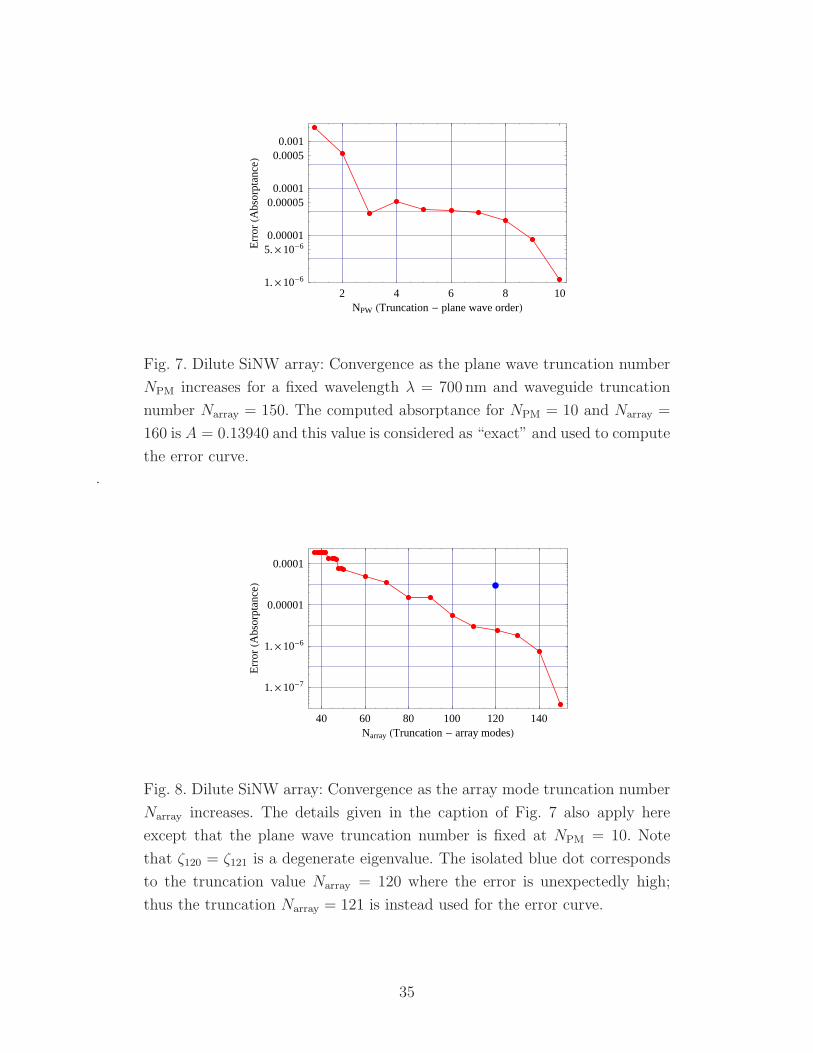
We have studied the convergence with respect to the truncation parameters of the plane
wave expansions and array mode expansions in Eqs (58) and (59). The array modes are
ordered in decreasing order with respect to Re ζ2n. We have used a circular truncation for
the plane wave truncation number NPM, i.e., for a given value of NPM, only the plane wave
orders (p, q) such that p2 + q2 ≤ N2PM are used in the truncated expansions; this choice is
motivated by the fact that, for normal incidence, it is consistent with the ordering of the
array modes since the plane wave propagation constants are given by the dispersion relation
γ2s = k2 − (p2 + q2) (2π/d)2 (see Eq. (11)); the propagation constants γs are also numbered
in decreasing value of −(p2 + q2).
Figures 7 and 8 illustrate the convergence when the number of plane wave orders and
the number of array modes used in modal expansions are increased. The wavelength is set
to λ = 700 nm and the corresponding silicon refractive index is n = 3.774 + 0.011 i, which
is taken from Ref. [26]. The error is estimated by assuming that the result obtained with
the highest discretization is “exact” (A = 0.13940 for NPM = 10 and Narray = 160). The
calculations are based on a highly refined FEM mesh consisting of 8088 triangles and 16361
nodes. In Fig. 8, there is a sudden jump in error when Narray = 120 (isolated blue dot); this
is due to the chosen truncation cutting through a pair of degenerate eigenvalue ζ120 = ζ121
i.e., including one member of the pair but excluding the other). Indeed the solution is well-
behaved when Narray = 121. Similar behavior has been observed when a pair of conjugate
eigenvalues is cut. Thus all members of a family of eigenvalues must be included together in
the modal expansion, otherwise there is degradation of the convergence, which is particularly
strong when it occurs for a low-order eigenvalue which makes a significant contribution to
the modal expansions. In practice we expect the computed absorptance to have about three
digits of accuracy when the truncation parameters of the plane wave expansions and array
mode expansions are set respectively to NPM = 3 (giving 29 plane wave orders and 2 × 29
basis functions for TE and TM polarizations) and Narray = 50, assuming adequate resolution
19

of the FEM mesh. The absorptance curve for the dilute SiNW array in Fig. 4 is obtained
using these truncation parameters and an FEM mesh which has 1982 triangles and 4061
nodes.
Figure 9 presents the absorptance spectrum for off-normal incidence (45). The absorp-
tance is sensitive to the angle of incidence and the light polarization. Compared with normal
incidence, the absorptance peak in the wavelength band [600 nm, 700 nm] (low silicon absorp-
tion) has shifted to shorter wavelengths while the peak near 400 nm (high silicon absorption)
has shifted to longer wavelengths.
3.C. Fano resonances in a photonic crystal slab
Fano resonances are well known from the field of particle physics [28], and they are observable
also in photonic crystals [29]. They are notable for their sharp spectral features and so serve
as a good benchmark for the accuracy of new numerical methods. We have carried out a
calculation of Fano resonances using our modal formulation. We present here an example
that was first studied by Fan and Joannopoulos [29]. The photonic crystal slab consists
of a square array of air holes in a background material of relative permittivity ǫ = 12.
Figure 10 shows the transmittance of a photonic crystal slab as a function of the normalized
frequency d/λ for a plane wave at normal incidence. The parameters of the slab considered
in Fig. 10 are identical to those in Fig. 12(a) of Ref. [29], and the curves from the two figures
are the same to visual accuracy. This is an additional validation of the approach presented
here. The transmittance curve reveals a strong transmission resonance which is typical of
asymmetric Fano resonances. These resonances are very sharp and can be used for switching
purposes [30].
4. Conclusion
We have developed a rigorous modal formulation for the diffraction of plane waves by absorb-
ing photonic crystal slabs. This approach combines the strongest aspects of two methods:
the computation of Bloch modes is handled numerically, using finite elements in a two-
dimensional context where this method excels, while the reflection and transmission of the
fields through the slab interfaces are handled semi-analytically, using a generalization of the
theory of thin films. This approach can lead to results achieved using a fraction of the compu-
tational resources of conventional algorithms: an example of this is given in Fig. 6, in which
a large number of different computations for different slab thicknesses were able to be com-
puted in a very short time. Although the speed-testing of this method against conventional
methods (FDTD and 3D Finite Element packages such as COMSOL) is a subject for future
work, we have demonstrated here the method’s accuracy and its rapidity of convergence. The
method also satisfies all internal checks related to reciprocity and conservation of energy, as
20

well as reproducing known results from the literature in challenging situations, such as the
simulation of Fano resonances (Fig. 10).
The method is very general with respect to the geometry of the structure. We have demon-
strated this by modeling both square and circular shaped inclusions. In addition, because
the method is at a fixed frequency, it can handle both dissipative and dispersive structures
in a straightforward manner, using tabulated values of the real and imaginary parts of the
refractive index. This is in contrast to time-domain methods such as FDTD, or to some
formulations of the finite element approach. Though we have used a single array type here
(the square array), other types of structure (such as hexagonal arrays) can be dealt with by
appropriately adjusting the unit cell Ω, together with the allowed range of Bloch modes.
It is also easy to see how this method could be extended to multiple slabs containing
different geometries, as well as taking into account the effect of one or more substrates; this
extension would involve the inclusion of field expansions for each layer, together with appro-
priate Fresnel matrices, in the equation system (77)-(80). In principle this approach could
then be used to study rods (or holes) whose radius or refractive index changed continuously
with depth, provided the spacing between the array cells remained constant.
Our method has an important advantage over purely numerical algorithms in that it gives
physical insight into the mechanisms of transmission and absorption in slabs of lossy periodic
media. The explanation of the absorption spectrum in arrays of silicon nanorods is vital for
the enhancement of efficiency of solar cells, however this spectrum is complicated, with
a number of processes, including coupling of light into the structure, Fabry-Perot effects,
and the overlap of the light with the absorbing material, all playing an important role. By
expanding in the natural eigenmodes of each layer of the structure, it is possible to isolate
these different effects and to identify criteria that the structure must satisfy in order to
efficiently absorb light over a specific wavelength range. This, we have discussed in a recent
related publication [25].
Acknowledgments
This research was conducted by the Australian Research Council Centre of Excellence for
Ultrahigh Bandwidth Devices for Optical Systems (project number CE110001018). We grate-
fully acknowledge the generous allocations of computing time from the National Computa-
tional Infrastructure (NCI) and from Intersect Australia.
21

A. Modal biorthogonality and normalization
Here we prove the biorthogonality of the modes and adjoint modes. Let us consider set of
modes (En,Hn) and adjoint modes (E†m,H
†m) of photonic crystal. These modes satisfy
∇×Hn = − ikεEn, (87a)
∇×En = ikµHn (87b)
and
∇×H†m = ikεE†
m, (88a)
∇×E†m = − ikµH†
m. (88b)
We multiply both sides of (87a) by E†m and (88a) by En and correspondingly we multiply
each set of (87b) by H†m and (88b) by Hn then adding these we deduce
∇ · (En ×H†m +E†
m ×Hn) = 0. (89)
Next we separate the transverse ⊥ and longitudinal ‖ (along the cylinder axes) components
according to
En = En⊥ +En‖, Hn = Hn⊥ +Hn‖, ∇ = ∇⊥ + ez∂
∂z. (90)
After the substitution of (90) into (89) we obtain
ez ·∂
∂z
[
En⊥ ×H†m⊥ + E
†m⊥ ×Hn⊥
]
= ∇⊥ ·[
En⊥ ×H†m‖ + En‖ ×H
†m⊥
+ E†m⊥ ×Hn‖ + E
†m‖ ×Hn⊥
]
. (91)
Taking into account the z-dependence on the modes given by the factors exp (iζnz),
exp (−iζ†mz) and integrating (91) over the unit cell we derive
i(ζn − ζ†m)
∫
Ω
ez · (En⊥ ×H†m⊥ +E
†m⊥ ×Hn⊥)dA = 0, (92)
since the integral on the left hand side vanishes due to quasi-periodicity. We finally obtain∫
Ω
ez · (En⊥ ×H†m⊥ +E
†m⊥ ×Hn⊥)dA = 0, (93)
which holds for arbitrary modes such that ζn 6= ζ†m.
The same relation holds for the counter propagating mode m
i(ζn + ζ†m)
∫
Ω
ez · (E−n⊥ ×H
†n⊥ +E
†m⊥ ×H−
n⊥)dA = 0. (94)
22

The minus sign in the superscript position indicates the direction of the propagation. Taking
into account the relations E−n⊥ = En⊥ and H−
n⊥ = −Hn⊥ we can rewrite (94) in the form∫
Ω
ez · (En⊥ ×H†m⊥ −E
†m⊥ ×Hn⊥)dA = 0. (95)
After subtraction of relation (95) from (94) the orthogonality relation takes form∫
Ω
ez · (E†m⊥ ×Hn⊥)dA = 0, (96)
which states that two distinct modes propagating in the same direction are orthogonal. It is
then clear that these modes can always be normalized such that∫
Ω
(ez ×Hn⊥) ·E†m⊥dA = δmn. (97)
B. Modal Completeness
From the field expansions we can derive the condition of the modal completeness. The plane
waves can be expanded in the following forms:
RE/M
s =∑
n
cE/Mn (ez ×H
†n⊥), (98)
RE/Ms =
∑
n
dE/Mn En⊥. (99)
By projecting Eq. (98) on the modes Em⊥ and using the biorthogonality relations Eq. (97)
we deduce (see Eq. (65))
cE/Mm =
∫
Ω
Em⊥ ·RE/M
s dA = JE/Msm . (100)
Similarly we project (99) onto the adjoint magnetic mode (ez ×H†m⊥) and deduce
dE/Mm =
∫
Ω
(ez ×H†m⊥) ·RE/M
s dA = KE/Mms . (101)
Thus,
RE/M
s =∑
n
KE/Mns (ez ×H
†n⊥), (102)
RE/Ms =
∑
n
JE/Mns En⊥. (103)
Next we project (99) onto plane wave basis by multiplying both sides of (99) by RE/M
s′
and integrating over the unit cell. We obtain∫
Ω
RE/Ms ·RE/M
s′ dA =∑
n
KE/Mns′
∫
Ω
En⊥ ·RE/M
s′ dA
=∑
n
KE/Mns′ J
E/Ms′n = δss′. (104)
23

The equation (104) represents the completeness relation for the modes. If we introduce the
vectors of matrices
J =
[
JE
JM
]
and K =
[
KE
KM
]
, (105)
where
JE/M =[
JE/Msm
]
and KE/M =[
KE/Msn
]
(106)
then the completeness relation Eq. (104) can be written in the matrix form
JK = I, (107)
where I is the identity matrix.
The completeness relation of the Rayleigh modes can be established in a similar way. The
transverse component of electric and magnetic modal fields can be represented as a series in
terms of Rayleigh modes in the region above the grid as
Em⊥ =∑
s
(
JEsmR
Es + JM
smRMs
)
, (108)
ez ×H†n⊥ =
∑
s
(
KEnsR
E
s +KMnsR
M
s
)
. (109)
By multiplying (108) on (109) and integrating we deduce∫
Ω
E†m⊥ · (ez ×Hn⊥ ) dA =
∑
s
(
JEsmKE
sn + JMsmKM
sn
)
= δnm. (110)
The completeness relation Eq. (110) can be written in matrix form
KJ = I. (111)
C. Interface and slab Energy conservation and reciprocity relations
Here we briefly outline the derivation of energy conservation relations for the situation when
there is no absorption. The flux conservation leads to the certain relations between the
Fresnel interface reflection and transmission matrices.
For some value z we can write an expansion
E⊥ =∑
n
(c−n + c+n )En⊥ (112)
and similarly
ez ×H⊥ =∑
n
(c−n − c+n )ez ×Hn⊥ (113)
24

The downward flux is defined by
Sz = Re
[∫
E⊥ · (ez × H⊥)
]
= (114)
1
2
[
(c− − c+)HU(c− + c+) + (c− + c+)HUH(c− − c+)]
,
where the matrix U is given by
Umn =
∫
Ω
Em⊥ · (ez ×Hn⊥)dA. (115)
The relation (114) can be written in the form
Sz = Re
[c−H c+H]V
[
c−
c+
]
, (116)
where matrix
V =
[
12(U +UH) 1
2(U −UH)
−12(U−UH) −1
2(U+UH)
]
(117)
is Hermitian, i.e. V H = V . This is a general result which is applicable also in the presence
of absorption. The U matrix is a dense matrix in the presence of absorption. In the absence
of absorption it reduces to the following structural form
U =
1 0 0 0 0 0 0 0 . . . 0
0 1 0 0 0 0 0 0 . . . 0
0 0 1 0 0 0 0 0 . . . 0
0 0 0 ±1 0 0 0 0 . . . 0
0 0 0 0 ±1 0 0 0 . . . 0
0 0 0 0 0 ±1 0 0 . . . 0
0 0 0 0 0 0 0 1 . . . 0
0 0 0 0 0 0 −1 0 . . . 0... . . .
...
0 . . . 0 1... . . . −1 0
.
(118)
as we show in Appendix D. Here we have ordered first the propagating modes with real
values of ζn, then evanescent modes with pure imaginary propagating constants ζn = ±i|ζn|and finally the evanescent modes with complex valued propagating constants ζn = ζ ′n + iζ ′′n.
25
Given the form of the U matrix Eq. (118) the expression for the flux Eq. (116) can be
expressed as
Sz = [c− c+]H
[
Im iIm
−iIm −Im
][
c−
c+
]
, (119)
where Im = Us - a diagonal matrix with unity on the propagating part of the diagonal of
U , while Im = Ua corresponds to the evanescent part of U [see Eq. (119)].
We next develop the energy conservation relations by considering the integration of fields
at the interface between free space and the semi-infinite photonic crystal. We write
c− = T12f− +R21c
+, (120)
f+ = R12f− + T21c
+, (121)
while[
c−
c+
]
=
[
T12 R21
0 I
][
f−
c+
]
. (122)
We also can rewrite the relation (121) in the matrix form[
f−
f+
]
=
[
I 0
R12 T21
][
f−
c+
]
, (123)
while the energy flux in the free space as
Sz = [f− f+]H
[
I1 iI1−iI1 −I1
][
f−
f+
]
. (124)
Now we substitute the relation for modal vector coefficients c± Eq. (122) into Eq. (119) and
the plane wave coefficients Eq. (123) into Eq. (124) then by equating the total fluxes in free
space Eq. (124) and in the photonic crystal Eq. (122) we can write[
I RH12
0 TH21
][
I1 −iI1iI1 −I1
][
I 0
R12 T21
]
=
[
TH12 0
RH21 I
][
I2 −iI2iI2 −I2
][
T12 R21
0 I
]
. (125)
where I2 = Im and I2 = Im and I1 as defined for the plane waves in Section 2.D.. Expandingthese and equating the formed partitions yields four conservation relations
RH12I1R12 + TH
12I2T12 = I1 + iRH12I1 − iI1R12, (126)
RH12I1T21 + TH
12I2R21 = iTH12I2 − iI1T21, (127)
RH21I2T12 + TH
21I1R12 = iTH21I1 − iI2T12, (128)
RH21I2R21 + TH
21I1T21 = I2 + iRH21I2 − iI2R21. (129)
26
The slab energy conservation relations can be found in the similar way as for the interface
relations as above. Furthermore the expressions of the energy relations are very similar to
the interface relations. The only difference is now the transmission T12 and the reflection
R12 matrices in (129) need to be replaced by the slab reflection and transmission matrices.
D. The flux matrix U
The adjoint modes are defined by
L†E†n = ζ2†n M†E†
n, (130)
with anti-quasi-periodicity condition E†(r +Rp) = E†(r) exp (−ik0 ·Rp) When there is no
absorption
LE†n = ζ2†n ME†
n (131)
given L† = L and M† = M are then self adjoint operators. Note that even though the
operators M and L are self adjoint (when there is no absorption) the eigenvalue problem
Eq. (131) is not Hermitian because the operator M−1L is not self adjoint in general. There-
fore the eigenvalues can be real representing propagating modes, as well as complex (pure
imaginary or complex) representing evanescent modes. Now from Eq. (131) we deduce
LE†n = ζ2†n ME
†n, (132)
where overline means complex conjugation. By comparing Eq. (132) and the original eigen-
value equation we deduce
E†nζ2 = E
nζ2 (133)
For the real eigenvalues ζ we choose ζ† = ζ while for complex ζ we must choose ζ† = −ζ
which will ensure that the downward evanescent propagating field is decaying. Therefore we
have
E†nζ = Enζ (134)
for the propagating field and
E†nζ = En,−ζ (135)
for the evanescent field. From Maxwell’s equations we deduce that
H†⊥nζ = −H⊥n,−ζ. (136)
27
Thus, the equations (92) and (94) can be rewritten as
(ζm − ζn)
∫
Ω
ez · (Em⊥ ×Hn⊥ +En⊥ ×Hm⊥)dA = 0,
(137)
(ζm + ζn)
∫
Ω
ez · (Em⊥ ×Hn⊥ −En⊥ ×Hm⊥)dA = 0
(138)
Therefore when ζm 6= ±ζ, by adding and subtracting the relations (137) and (138) we may
deduce∫
Ω
ez · (Em⊥ ×Hn⊥)dA =
∫
Ω
ez · (En⊥ ×Hm⊥)dA = 0, (139)
which are the Umn elements of the matrix U introduced earlier. From (138) and for ζm = ζnand real ζn we deduce that the integral
∫
Ω
ez · (En⊥ ×Hn⊥)dA (140)
is real. When ζm is pure imaginary and ζm = ζn = iζ then from (138) we deduce that
∫
Ω
ez · (En⊥ ×Hn⊥)dA (141)
is pure imaginary.
Now let us consider the case where ζn is complex. The U matrix is defined by (115). For
modes ζm = ζ and ζn = −ζ from (115) and (136) we deduce
Umn =
∫
Ω
Eζ⊥ · (ez ×H−ζ⊥)dA = −∫
Ω
Eζ⊥ · (ez ×H†ζ⊥)dA. (142)
By using the orthonormal condition
∫
Ω
Eζ⊥ · (ez ×H†ζ⊥)dA = 1 (143)
we find Uζm,ζn = Uζ,−ζ = −1.
For the modes ζm = −ζ and ζn = ζ from (115) we obtain
Umn =
∫
Ω
E−ζ⊥ · (ez ×Hζ⊥)dA
=
∫
Ω
E†ζ⊥ · (ez ×Hζ⊥)dA = 1. (144)
So the elements Uζm,ζn = U−ζ,ζ, = 1. This means that (U +UH)/2 is a diagonal matrix with
unit elements on only the corresponding to propagating modal part.
28

References
1. J. D. Joannopoulos, R. D. Meade, and J. N. Winn, Photonic Crystals: Molding the Flow
of Light (Princeton University Press, New Jersey, 1995).
2. T. Asano, B.-S. Song, and S. Noda, “Analysis of the experimental Q factors (∼1 million)
of photonic crystal nanocavities,” Opt. Express 14, 1996–2002 (2006).
3. T. F. Krauss, “Slow light in photonic crystal waveguides,” Journal of Physics D 40, 2666
(2007).
4. Z. Yu, A. Raman, and S. Fan, “Fundamental limit of light trapping in grating structures,”
Opt. Express 18, A366–A380 (2010).
5. E. Yablonovitch, “Statistical ray optics,” J. Opt. Soc. Am. 72, 899–907 (1982).
6. S. Nishimura, N. Abrams, B. A. Lewis, L. I. Halaoui, T. E. Mallouk, K. D. Benkstein,
J. van de Lagemaat, and A. J. Frank, “Standing wave enhancement of red absorbance
and photocurrent in dye-sensitized titanium dioxide photoelectrodes coupled to photonic
crystals,” J. Am. Chem. Soc. 125, 6306–6310 (2003).
7. A. Chutinan and S. John, “Light trapping and absorption optimization in certain thin-
film photonic crystal architectures,” Phys. Rev. A 78, 023825 (2008).
8. B. Tian, X. Zheng, T. J. Kempa, Y. Fang, N. Yu, G. Yu, J. Huang, and C. M. Lieber,
“Coaxial silicon nanowires as solar cells and nanoelectronic power sources,” Nature 449,
885–889 (2007).
9. C. Lin and M. L. Povinelli, “Optical absorption enhancement in silicon nanowire arrays
with a large lattice constant for photovoltaic applications,” Opt. Express 17, 19371–
19381 (2009).
10. N. S. Lewis, “Toward cost-effective solar energy use,” Science 315, 798–801 (2007).
11. P. Wurfel, Physics of Solar Cells: From Basic Principles to Advanced Concepts (Vch
Verlagsgesellschaft Mbh, 2009).
12. J. Li, H. Yu, S. M. Wong, X. Li, G. Zhang, P. G.-Q. Lo, and D.-L. Kwong, “Design
guidelines of periodic Si nanowire arrays for solar cell application,” Appl. Phys. Lett.
95, 243113 (2009).
13. R. C. McPhedran, D. H. Dawes, L. C. Botten, and N. A. Nicorovici, “On-axis diffrac-
tion by perfectly conducting capacitive grids,” Journal of Electromagnetic Waves and
Applications 10, 1085–1111(27) (1996).
14. L. C. Botten, R. C. McPhedran, N. A. Nicorovici, and A. B. Movchan, “Off-axis diffrac-
tion by perfectly conducting capacitive grids: Modal formulation and verification,” Jour-
nal of Electromagnetic Waves and Applications 12, 847–882(36) (1998).
15. P. M. Morse and H. Feshbach, Methods of Theoretical Physics, Part I (McGraw-Hill,
1953).
29

16. J. Blad and A. S. Sudbø, “Evanescent modes in out-of-plane band structure for two-
dimensional photonic crystals,” Opt. Express 17, 7170–7185 (2009).
17. D. J. Kan, A. A. Asatryan, C. G. Poulton, and L. C. Botten, “Multipole method for
modeling linear defects in photonic woodpiles,” J. Opt. Soc. Am. B 27, 246–258 (2010).
18. L. C. Botten, M. S. Craig, R. C. McPhedran, J. L. Adams, and J. R. Andrewartha, “The
finitely conducting lamellar diffraction grating,” Opt. Acta 28, 1087–1102 (1981).
19. L. Vardapetyan and L. Demkowicz, “Full-wave analysis of dielectric waveguides at a
given frequency,” Math. Comp. 72, 105–129 (electronic) (2003).
20. K. Dossou and M. Fontaine, “A high order isoparametric finite element method for the
computation of waveguide modes,” Comput. Methods Appl. Mech. Engrg. 194, 837–858
(2005).
21. R. B. Lehoucq, D. C. Sorensen, and C. Yang, ARPACK users’ guide (Society for Indus-
trial and Applied Mathematics (SIAM), Philadelphia, PA, 1998).
22. A. Bossavit, Computational Electromagnetism: Variational Formulations, Complemen-
tarity, Edge Elements (Academic Press, 1998).
23. D. Boffi, F. Brezzi, L. F. Demkowicz, R. G. Duran, R. S. Falk, and M. Fortin,Mixed finite
elements, compatibility conditions, and applications (Springer-Verlag, Berlin, 2008).
24. G. W. Hanson and A. B. Yakovlev, Operator theory for electromagnetics : an introduction
(Springer, 2002).
25. B. C. P. Sturmberg, K. B. Dossou, L. C. Botten, A. A. Asatryan, C. G. Poulton, C. M.
de Sterke, and R. C. McPhedran, “Modal analysis of enhanced absorption in silicon
nanowire arrays,” Opt. Express 19, A1067–A1081 (2011).
26. M. A. Green and M. J. Keevers, “Optical properties of intrinsic silicon at 300 K,” Progress
in Photovoltaics: Research and Applications 3, 189–192 (1995).
27. J. Meixner, “The behavior of electromagnetic fields at edges,” IEEE Trans. Antennas
Propag. 20, 442 – 446 (1972).
28. U. Fano, “Effects of configuration interaction on intensities and phase shifts,” Phys. Rev.
124, 1866–1878 (1961).
29. S. Fan and J. D. Joannopoulos, “Analysis of guided resonances in photonic crystal slabs,”
Phys. Rev. B 65, 235112 (2002).
30. R. Asadi, M. Malek-Mohammad, and S. Khorasani, “All optical switch based on Fano
resonance in metal nanocomposite photonic crystals,” Opt. Comm. 284, 2230–2235
(2011).
30

List of Figures
1 Geometry of the problem. The dielectric permittivity and the magnetic per-
meability of the slab can be dispersive and can have absorption. The unit
cell of the array (right panel) can have arbitrary number of inclusions with
arbitrary shapes. The direction of the plane wave incident from above the
structure can be arbitrarily chosen. . . . . . . . . . . . . . . . . . . . . . . . 32
2 Schematic of the field representation near the top and bottom interfaces. . . 32
3 Dispersion curves (lossless cylinders). The solid red curves represent solutions
such that ζ2 is real. The dashed blue curves represent solutions such that
Im(ζ2) is not zero. The complex solutions ζ2 occur as conjugate pairs and, in
order to differentiate the pairs, we use the term Re(ζ2)+ Im(ζ2) for the x-axis
instead of Re(ζ2). . . . . . . . . . . . . . . . . . . . . . . . . . . . . . . . . 33
4 Dotted black curve is the absorption spectrum at normal incidence for a dilute
SiNW array (silicon fill fraction is approximately 3.1%). For comparison, the
absorptance curves of a homogeneous slab of equal thickness (thin blue curve)
and of a homogeneous slab comprising equal volume of silicon (thick red curve)
are shown. . . . . . . . . . . . . . . . . . . . . . . . . . . . . . . . . . . . . . 33
5 The black dotted curve and the red solid curve are the absorption spectrum,
at normal incidence, of dilute SiNW arrays consisting respectively of circular
cylinders with radius a = 60 nm and square cylinders with side length a√π.
The two types of cylinders have the same cross section area and the same
height. . . . . . . . . . . . . . . . . . . . . . . . . . . . . . . . . . . . . . . 34
6 Dilute SiNW array: Contour plot of the absorptance as a function of the
wavelength and the cylinder height h. The cylinder radius and the lattice
constant are respectively a = 60 nm and d = 600 nm. . . . . . . . . . . . . . 34
7 Dilute SiNW array: Convergence as the plane wave truncation number NPM
increases for a fixed wavelength λ = 700 nm and waveguide truncation number
Narray = 150. The computed absorptance for NPM = 10 and Narray = 160 is
A = 0.13940 and this value is considered as “exact” and used to compute the
error curve. . . . . . . . . . . . . . . . . . . . . . . . . . . . . . . . . . . . . 35
8 Dilute SiNW array: Convergence as the array mode truncation number Narray
increases. The details given in the caption of Fig. 7 also apply here except that
the plane wave truncation number is fixed at NPM = 10. Note that ζ120 = ζ121
is a degenerate eigenvalue. The isolated blue dot corresponds to the truncation
value Narray = 120 where the error is unexpectedly high; thus the truncation
Narray = 121 is instead used for the error curve. . . . . . . . . . . . . . . . . 35
31

d
d
Fig. 1. Geometry of the problem. The dielectric permittivity and the magnetic
permeability of the slab can be dispersive and can have absorption. The unit
cell of the array (right panel) can have arbitrary number of inclusions with
arbitrary shapes. The direction of the plane wave incident from above the
structure can be arbitrarily chosen.
f 1- f 1
+
c- P c+
P c- c+
f 2-
Fig. 2. Schematic of the field representation near the top and bottom interfaces.
9 Off-normal incidence on a dilute SiNW: Absorption spectrum for 45 off-
normal orientated along x-axis (azimuthal angle = 0). The solid red and
dashed blue curves represent an incidence by TE-polarized and TM-polarized
plane wave respectively. The absorption spectrum for normal incidence (Fig. 4)
is also shown (dotted black). . . . . . . . . . . . . . . . . . . . . . . . . . . 36
10 Fano resonances: Transmittance versus normalized frequency for the normal
incidence. The radius of the cylinders is a/d = 0.05. The resonances in trans-
mission are well resolved. . . . . . . . . . . . . . . . . . . . . . . . . . . . . 36
32

-3 -2 -1 0 1 2HReHΖ2L+ImHΖ2LL H2ΠdL2
0
0.5
1
1.5
2
d2
Λ2
Fig. 3. Dispersion curves (lossless cylinders). The solid red curves represent
solutions such that ζ2 is real. The dashed blue curves represent solutions such
that Im(ζ2) is not zero. The complex solutions ζ2 occur as conjugate pairs
and, in order to differentiate the pairs, we use the term Re(ζ2) + Im(ζ2) for
the x-axis instead of Re(ζ2).
300 400 500 600 700 800 900 1000 1100Wavelength HnmL
0.2
0.4
0.6
0.8
1
Abs
orpt
ance
Fig. 4. Dotted black curve is the absorption spectrum at normal incidence for a
dilute SiNW array (silicon fill fraction is approximately 3.1%). For comparison,
the absorptance curves of a homogeneous slab of equal thickness (thin blue
curve) and of a homogeneous slab comprising equal volume of silicon (thick
red curve) are shown.
33

300 400 500 600 700 800 900 1000 1100Wavelength HnmL
0.2
0.4
0.6
0.8
1
Abs
orpt
ance
Fig. 5. The black dotted curve and the red solid curve are the absorption
spectrum, at normal incidence, of dilute SiNW arrays consisting respectively
of circular cylinders with radius a = 60 nm and square cylinders with side
length a√π. The two types of cylinders have the same cross section area and
the same height.
400 600 800 1000Wavelength HnmL
0
0.5
1
1.5
2
2.5
3
Hei
ghtHΜ
mL
0.0
0.97
Fig. 6. Dilute SiNW array: Contour plot of the absorptance as a function of
the wavelength and the cylinder height h. The cylinder radius and the lattice
constant are respectively a = 60 nm and d = 600 nm.
34
2 4 6 8 10NPW HTruncation - plane wave orderL
1.´10-6
5.´10-60.00001
0.000050.0001
0.00050.001
Err
orHA
bsor
ptan
ceL
Fig. 7. Dilute SiNW array: Convergence as the plane wave truncation number
NPM increases for a fixed wavelength λ = 700 nm and waveguide truncation
number Narray = 150. The computed absorptance for NPM = 10 and Narray =
160 is A = 0.13940 and this value is considered as “exact” and used to compute
the error curve.
.
40 60 80 100 120 140Narray HTruncation - array modesL
1.´10-7
1.´10-6
0.00001
0.0001
Err
orHA
bsor
ptan
ceL
Fig. 8. Dilute SiNW array: Convergence as the array mode truncation number
Narray increases. The details given in the caption of Fig. 7 also apply here
except that the plane wave truncation number is fixed at NPM = 10. Note
that ζ120 = ζ121 is a degenerate eigenvalue. The isolated blue dot corresponds
to the truncation value Narray = 120 where the error is unexpectedly high;
thus the truncation Narray = 121 is instead used for the error curve.
35

300 400 500 600 700 800 900Wavelength HnmL
0.2
0.4
0.6
0.8
1
Abs
orpt
ance
Fig. 9. Off-normal incidence on a dilute SiNW: Absorption spectrum for 45
off-normal orientated along x-axis (azimuthal angle = 0). The solid red and
dashed blue curves represent an incidence by TE-polarized and TM-polarized
plane wave respectively. The absorption spectrum for normal incidence (Fig. 4)
is also shown (dotted black).
0.25 0.3 0.35 0.4 0.45 0.5 0.55 0.6dΛ
0.2
0.4
0.6
0.8
1
Tra
nsm
ittan
ce
Fig. 10. Fano resonances: Transmittance versus normalized frequency for the
normal incidence. The radius of the cylinders is a/d = 0.05. The resonances in
transmission are well resolved.
36