mixed-signal control processor with arm cortex-m4
TRANSCRIPT

Preliminary Technical Data
Mixed-Signal Control Processorwith ARM Cortex-M4
ADSP-CM402F/CM403F/CM407F/CM408F
Rev. PrEInformation furnished by Analog Devices is believed to be accurate and reliable.However, no responsibility is assumed by Analog Devices for its use, nor for anyinfringements of patents or other rights of third parties that may result from its use.Specifications subject to change without notice. No license is granted by implicationor otherwise under any patent or patent rights of Analog Devices. Trademarks andregistered trademarks are the property of their respective owners.
One Technology Way, P.O. Box 9106, Norwood, MA 02062-9106 U.S.A.Tel: 781.329.4700 www.analog.comFax: 781.461.3113 © 2013 Analog Devices, Inc. All rights reserved.
SYSTEM FEATURES
100 MHz to 240 MHz ARM Cortex-M4 with floating-point unit 128K Byte to 384K Byte zero-wait-state L1 SRAM with
16K Byte L1 cacheUp to 2M Byte flash memory16-bit asynchronous external memory interfaceEnhanced PWM unitsFour 3rd/4th order SINC filters for glueless connection of iso-
lated ADCsHarmonic analysis engine10/100 Ethernet MACFull Speed USB On-the-Go (OTG)Two CAN (controller area network) 2.0B interfacesThree UART ports
Two Serial Peripheral Interface (SPI-compatible) portsEight 32-bit general-purpose timersFour Encoder Interfaces, 2 with frequency divisionSingle power supply176-lead (24 mm × 24 mm) RoHS compliant LQFP package120-lead (14 mm × 14 mm) RoHS compliant LQFP package
ANALOG SUBSYSTEM FEATURES
ADC controller (ADCC) and DAC controller (DACC)Two 16-bit SAR ADCs with up to 24 multiplexed inputs,
supporting dual simultaneous conversion in 380 ns (16-bit, no missing codes, ±3.5LSB INL)
Two 12-bit R-string DACs, with output rate up to 50 kHzTwo 2.5 V precision voltage reference outputs(For details, see ADC/DAC Specifications on Page 36.)
Figure 1. Block Diagram
UP TO 2M BYTEFLASH
L1 CACHE
16K BYTEL1 INSTRUCTION
CACHE
SYSTEM CONTROL BLOCKS
PERIPHERALS
HARDWARE FUNCTIONS
L3 MEMORY
SYSTEM FABRIC1× EMAC WITH
IEEE 1588(OPTIONAL)
2x SPORT
2× CAN
STATIC MEMORYCONTROLLER
ASYNC INTERFACE
2× SPI
4× QUADRATUREENCODER
8× TIMER
12× PWM PAIRS
1× TWI
USB FS OTG(OPTIONAL)
L1 MEMORY
UP TO 384K BYTE PARITY-ENABLED
ZERO-WAIT-STATE SRAM
CoreSight™TEST & CONTROL
PLL & POWERMANAGEMENT
FAULTMANAGEMENT
EVENTCONTROL
SYSTEMWATCHDOGS
3× UART
ADCC DACC
HARMONIC ANALYSIS ENGINE(HAE)
ANALOG SUBSYSTEM
GPI
O (4
0 O
R 9
1)
ADC DAC
Cortex-M4
SINC FILTERS

Rev. PrE | Page 2 of 84 | September 2013
ADSP-CM402F/CM403F/CM407F/CM408F Preliminary Technical Data
TABLE OF CONTENTSSystem Features . . . . . . . . . . . . . . . . . . . . . . . . . . . . . . . . . . . . . . . . . . . . . . . . . . . . . . . 1Analog Subsystem Features . . . . . . . . . . . . . . . . . . . . . . . . . . . . . . . . . . . . . . . . 1General Description . . . . . . . . . . . . . . . . . . . . . . . . . . . . . . . . . . . . . . . . . . . . . . . . . 3
Analog Subsystem .. . . . . . . . . . . . . . . . . . . . . . . . . . . . . . . . . . . . . . . . . . . . . . . . 4ARM Cortex-M4 Core . . . . . . . . . . . . . . . . . . . . . . . . . . . . . . . . . . . . . . . . . . . 7EmbeddedICE . . . . . . . . . . . . . . . . . . . . . . . . . . . . . . . . . . . . . . . . . . . . . . . . . . . . . . 7Processor Infrastructure . . . . . . . . . . . . . . . . . . . . . . . . . . . . . . . . . . . . . . . . . 7Memory Architecture . . . . . . . . . . . . . . . . . . . . . . . . . . . . . . . . . . . . . . . . . . . . 8Security Features . . . . . . . . . . . . . . . . . . . . . . . . . . . . . . . . . . . . . . . . . . . . . . . . 10Processor Reliability Features . . . . . . . . . . . . . . . . . . . . . . . . . . . . . . . . . 10Additional Processor Peripherals . . . . . . . . . . . . . . . . . . . . . . . . . . . . 11General-Purpose Counters . . . . . . . . . . . . . . . . . . . . . . . . . . . . . . . . . . . . 12Serial Peripheral Interface (SPI) Ports . . . . . . . . . . . . . . . . . . . . . . 12UART Ports . . . . . . . . . . . . . . . . . . . . . . . . . . . . . . . . . . . . . . . . . . . . . . . . . . . . . . 12TWI Controller Interface . . . . . . . . . . . . . . . . . . . . . . . . . . . . . . . . . . . . . . 12Controller Area Network (CAN) . . . . . . . . . . . . . . . . . . . . . . . . . . . . 1310/100 Ethernet MAC .. . . . . . . . . . . . . . . . . . . . . . . . . . . . . . . . . . . . . . . . . 13USB 2.0 On-the-Go Dual-Role Device Controller . . . . . . . 13Clock and Power Management . . . . . . . . . . . . . . . . . . . . . . . . . . . . . . . 14System Debug . . . . . . . . . . . . . . . . . . . . . . . . . . . . . . . . . . . . . . . . . . . . . . . . . . . . 15Development Tools . . . . . . . . . . . . . . . . . . . . . . . . . . . . . . . . . . . . . . . . . . . . . 15
Related Documents . . . . . . . . . . . . . . . . . . . . . . . . . . . . . . . . . . . . . . . . . . . . . . 15Related Signal Chains . . . . . . . . . . . . . . . . . . . . . . . . . . . . . . . . . . . . . . . . . . . 16
ADSP-CM402F/ADSP-CM403F Signal Descriptions . . . . . . 17ADSP-CM402F/ADSP-CM403F Multiplexed Pins . . . . . . . . . 22ADSP-CM407F/ADSP-CM408F Signal Descriptions . . . . . . 24ADSP-CM407F/ADSP-CM408F Multiplexed Pins . . . . . . . . . 31Specifications . . . . . . . . . . . . . . . . . . . . . . . . . . . . . . . . . . . . . . . . . . . . . . . . . . . . . . . . 34
Operating Conditions . . . . . . . . . . . . . . . . . . . . . . . . . . . . . . . . . . . . . . . . . . . 34Electrical Characteristics . . . . . . . . . . . . . . . . . . . . . . . . . . . . . . . . . . . . . . . 35ADC/DAC Specifications . . . . . . . . . . . . . . . . . . . . . . . . . . . . . . . . . . . . . . 36Flash Specifications . . . . . . . . . . . . . . . . . . . . . . . . . . . . . . . . . . . . . . . . . . . . . . 43Absolute Maximum Ratings . . . . . . . . . . . . . . . . . . . . . . . . . . . . . . . . . . . 44ESD Sensitivity . . . . . . . . . . . . . . . . . . . . . . . . . . . . . . . . . . . . . . . . . . . . . . . . . . . 44Package Information . . . . . . . . . . . . . . . . . . . . . . . . . . . . . . . . . . . . . . . . . . . . 44Timing Specifications . . . . . . . . . . . . . . . . . . . . . . . . . . . . . . . . . . . . . . . . . . . 45Output Drive Currents . . . . . . . . . . . . . . . . . . . . . . . . . . . . . . . . . . . . . . . . . 72Environmental Conditions . . . . . . . . . . . . . . . . . . . . . . . . . . . . . . . . . . . . 73
120-Lead LQFP Lead Assignments . . . . . . . . . . . . . . . . . . . . . . . . . . . . . 74176-Lead LQFP Lead Assignments . . . . . . . . . . . . . . . . . . . . . . . . . . . . . 77Outline Dimensions . . . . . . . . . . . . . . . . . . . . . . . . . . . . . . . . . . . . . . . . . . . . . . . . 81Pre-Release Products . . . . . . . . . . . . . . . . . . . . . . . . . . . . . . . . . . . . . . . . . . . . . . . 82
REVISION HISTORY
09/13—Revision PrD to Revision PrEUpdated the Specifications section to include Flash information and timing data for all interfaces. See Specifications . . . . . . . 34

Preliminary Technical Data
Rev. PrE | Page 3 of 84 | September 2013
ADSP-CM402F/CM403F/CM407F/CM408F
GENERAL DESCRIPTIONThe ADSP-CM40x family of mixed-signal control processors is based on the ARM® Cortex-M4TM processor core with floating-point unit operating at frequencies up to 240 MHz and integrat-ing up to 384KB of SRAM memory, 2MB of flash memory, accelerators and peripherals optimized for motor control and photo-voltaic (PV) inverter control and an analog module con-sisting of two 16-bit SAR-type ADCs and two 12-bit DACs. The ADSP-CM40x family operates from a single voltage supply (VDD_EXT/VDD_ANA), generating its own internal voltage supplies using internal voltage regulators and an external pass transistor.This family of mixed-signal control processors offers low static power consumption and is produced with a low-power and low-voltage design methodology, delivering world class processor and ADC performance with lower power consumption. By integrating a rich set of industry-leading system peripherals and memory (shown in Table 1), the ADSP-CM40x mixed-sig-nal control processors are the platform of choice for
next-generation applications that require RISC programmabil-ity, advanced communications and leading-edge signal processing in one integrated package. These applications span a wide array of markets including power/motor control, embed-ded industrial, instrumentation, medical and consumer.Each ADSP-CM40x family member contains the following modules.
• 8 GP timers with PWM output• 3-Phase PWM units with up to 4 output pairs per unit• 2 CAN modules• 1 two-wire interface (TWI) module• 3 UARTs
Table 1 provides the additional product features shown by model.
Table 1. ADSP-CM40x Family Product Features
Generic ADSP-CM402F ADSP-CM403F ADSP-CM407F ADSP-CM408F
Package 120-Lead LQFP 176-Lead LQFP
GPIOs 40 91
EBIU 16-bit Asynchronous/5 Address 16-Bit Asynchronous/24 Address
ADC ENOB (no averaging) 11+ 13+ 11+ 13+
ADC Inputs 24 16
DAC Outputs 2 N/A
SPORTs 3 Half-SPORTs 4 Half-SPORTs
Ethernet N/A 1 N/A N/A 1 N/A
USB N/A 1 1 N/A 1 1
External SPI 1 2
General-Purpose Counters 2 4 (2 with dual-outputs)
Feature Set Code E F C E F A B D A B
L1 SRAM (KB) 128 128 384 128 128 384 384 128 384 384
Flash (KB) 512 256 2048 512 256 2048 2048 1024 2048 2048
Core Clock (MHz) 150 100 240 150 100 240 240 150 240 240
Model
AD
SP-CM
402BSWZ-EF
AD
SP-CM
402BSWZ-FF
AD
SP-CM
403BSWZ-C
F
AD
SP-CM
403BSWZ-EF
AD
SP-CM
403BSWZ-FF
AD
SP-CM
407BSWZ-A
F
AD
SP-CM
407BSWZ-BF
AD
SP-CM
407BSWZ-D
F
AD
SP-CM
408BSWZ-A
F
AD
SP-CM
408BSWZ-BF

Rev. PrE | Page 4 of 84 | September 2013
ADSP-CM402F/CM403F/CM407F/CM408F Preliminary Technical Data
ANALOG SUBSYSTEM
The processors contain two ADCs and two DACs. Control of these data converters is simplified by a powerful on-chip ana-log-to-digital conversion controller (ADCC) and a digital-to-analog conversion controller (DACC). The ADCC and DACC are integrated seamlessly into the software programming model, and they efficiently manage the configuration and real-time operation of the ADCs and DACs. For technical details, see ADC/DAC Specifications on Page 36.The ADCC provides the mechanism to precisely control execu-tion of timing and analog sampling events on the ADCs. The ADCC supports two-channel (one each—ADC0, ADC1) simul-taneous sampling of ADC inputs with TBD ps time offset accuracy (aperture delay), and can deliver 16 channels of ADC data to memory in 3 μS. Conversion data from the ADCs may be either routed via DMA to memory, or to a destination regis-ter via the processor. The ADCC can be configured so that the
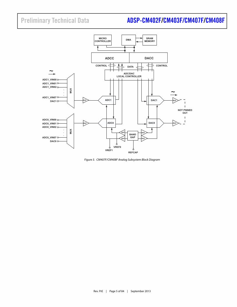
two ADCs sample and convert both analog inputs simultane-ously or at different times and may be operated in asynchronous or synchronous modes. The best performance can be achieved in synchronous mode.Likewise, the DACC interfaces to two DACs and has purpose of managing those DACs. Conversion data to the DACs may be either routed from memory through DMA, or from a source register via the processor.Functional operation and programming for the ADCC and DACC are described in detail in the ADSP-CM40x Mixed-Signal Control Processor with ARM Cortex-M4 Hardware Reference.ADC and DAC features and performance specifications differ by processor model. Simplified block diagrams of the ADCC, DACC and the ADCs and DACs are shown in Figure 2 and Figure 3.
Figure 2. CM402F/CM403F Analog Subsystem Block Diagram
DAC1
DAC0ADC0
ADC1_VIN00
.
.
.
ADC1_VIN01ADC1_VIN02
ADC1_VIN11DAC1
ADC0_VIN00
.
.
.
ADC0_VIN01ADC0_VIN02
ADC0_VIN11DAC0
MU
X M
UX
ADCC DACC
CONTROL CONTROL
MICROCONTROLLER DMA SRAM
MEMORY
DATA
VREF1VREF0
REFCAP
BUF
BUF
BUF
BUF
BUFBUF
DAC1_VOUT
DAC0_VOUT
~
~
~
ADC1
BUFBUF
BANDGAP
ADC/DACLOCAL CONTROLLER
Preliminary Technical Data
Rev. PrE | Page 5 of 84 | September 2013
ADSP-CM402F/CM403F/CM407F/CM408F
Figure 3. CM407F/CM408F Analog Subsystem Block Diagram
DAC1
DAC0
ADC1
ADC0
ADC1_VIN00
.
.
.
ADC1_VIN01ADC1_VIN02
ADC1_VIN07DAC1
ADC0_VIN00
.
.
.
ADC0_VIN01ADC0_VIN02
ADC0_VIN07DAC0
MU
XM
UX
ADCC DACC
CONTROL CONTROL
MICROCONTROLLER DMA SRAM
MEMORY
DATA
VREF1VREF0
REFCAP
BUF
BUF
BUF
BUF
BUFBUF
~
~
NOT PINNEDOUT
BUFBUF
BANDGAP
ADC/DACLOCAL CONTROLLER

Rev. PrE | Page 6 of 84 | September 2013
ADSP-CM402F/CM403F/CM407F/CM408F Preliminary Technical Data
Considerations for Best Converter Performance
As with any high performance analog/digital circuit, to achieve best performance, good circuit design and board layout prac-tices should be followed. The power supply and its noise bypass (decoupling), ground return paths and pin connections, and analog/digital routing channel paths and signal shielding, are all of first-order consideration. For application hints of design best practice, see Figure 4 and the ADSP-CM40x Mixed-Signal Con-trol Processor with ARM Cortex-M4 Hardware Reference.
ADC Module
The ADC module contains two 16-bit, high speed, low power successive approximation register (SAR) ADCs, allowing for dual simultaneous sampling with each ADC proceeded by a 12-channel multiplexer. See ADC Specifications on Page 36 for detailed performance specifications. Input multiplexers enable up to a combined 26 analog input sources to the ADCs (12 ana-log inputs plus 1 DAC loopback input per ADC). The voltage input range requirement for those analog inputs is from 0 V to 2.5 V. All analog inputs are of single-ended design. As with all single-ended inputs, signals from high impedance sources are the most difficult to control, and depending on the
electrical environment, may require an external buffer circuit for signal conditioning (Figure 5). An on-chip buffer between the multiplexer and ADC reduces the need for additional signal conditioning external to the processor. Additionally, each ADC has an on-chip 2.5 V reference that can be overdriven when an external voltage reference is preferred.
DAC Module
The DAC is a 12-bit, low power, string DAC design. The output of the DAC is buffered, and can drive an R/C load to either ground or VDD_ANA. See DAC Specifications on Page 38 for detailed performance specifications. It should be noted that on some models of the processor, the DAC outputs are not pinned out. However, these outputs are always available as one of the multiplexed inputs to the ADCs. This feature may be useful for functional self-check of the converters.
Figure 4. Typical Power Supply Configuration
Figure 5. Equivalent Single-Ended Input (Simplified)
VDD_EXT
VDD_VREG
VDD_INT
BYP_D0
GND
VDD_ANA0
GND_ANA0
BYP_A0
VREF0
VREF_GND0
REFCAP
VREF1_GND
VREF1
BYP_A1
GND_ANA1
VDD_ANA1
VREG
CIR
CU
IT
GND_ANA
3.3V
CONNECTEDAT ONEPOINT
GND_DIGPLANE
GND_ANAPLANE
GND_DIG
GND_ANA2GND_ANA3
VREG_BASE
ADSP-CM40x
ANALOGSOURCE
TOADCVIN
VDD_ANA
CTBD
OPTIONALEXTERNAL
BUFFER
C
HOLD
RTRACK
CIN
RIN TBD
TBD
ADSP-CM40x

Preliminary Technical Data
Rev. PrE | Page 7 of 84 | September 2013
ADSP-CM402F/CM403F/CM407F/CM408F
Harmonic Analysis Engine (HAE)
The Harmonic Analysis Engine (HAE) block receives 8 kHz input samples from two source signals whose frequencies are between 45 Hz and 65 Hz. The HAE will then process the input samples and produce output results. The output results consist of power quality measurements of the fundamental and up to 12 additional harmonics.
SINC Filter
The SINC module processes four bit streams using a pair of configurable SINC filters for each bitstream. The purpose of the primary SINC filter of each pair is to produce the filtered and decimated output for the pair. The output may be decimated to any integer rate between 8 and 256 times lower than the input rate. Greater decimation allows greater removal of noise and therefore greater ENOB.Optional additional filtering outside the SINC module may be used to further increase ENOB. The primary SINC filter output is accessible through transfer to processor memory, or to another peripheral, via DMA.Each of the four channels is also provided with a low-latency secondary filter with programmable positive and negative over-range detection comparators. These limit detection events can be used to interrupt the core, generate a trigger, or signal a sys-tem fault.
ARM CORTEX-M4 CORE
The ARM Cortex-M4, core shown in Figure 6, is a 32-bit reduced instruction set computer (RISC). It uses a single 32-bit bus for instruction and data. The length of the data can be eight bits, 16 bits, or 32 bits. The length of the instruction word is 16 or 32 bits. The controller has the following features.
Cortex-M4 Architecture
• Thumb-2 ISA Technology• DSP and SIMD extensions• Single cycle MAC (Up to 32 × 32 + 64 -> 64)• Hardware Divide Instructions• Single-precision FPU• NVIC Interrupt Controller (129 Interrupts and
16 Priorities)• Memory Protection Unit (MPU)• Full CoreSightTM Debug, Trace, Breakpoints, Watchpoints,
and Cross-Triggers
Microarchitecture
• 3-stage pipeline with branch speculation• Low-latency interrupt processing with tail chaining
Configurable For Ultra Low Power
• Deep sleep mode, dynamic power management• Programmable Clock Generator Unit
EmbeddedICE
EmbeddedICE® provides integrated on-chip support for the core. The EmbeddedICE module contains the breakpoint and watch-point registers that allow code to be halted for debugging purposes. These registers are controlled through the JTAG test port.When a breakpoint or watchpoint is encountered, the processor halts and enters debug state. Once in a debug state, the proces-sor registers can be inspected as well as the Flash/EE, SRAM, and memory mapped registers.
PROCESSOR INFRASTRUCTURE
The following sections provide information on the primary infrastructure components of the ADSP-CM40x processors.
DMA Controllers (DDEs)
The processor contains 17 peripheral DMA channels plus two MDMA streams. DDE channel numbers 0–16 are for peripher-als and channels 17–20 are for MDMA.
System Event Controller (SEC)
The SEC manages the enabling and routing of system fault sources through its integrated fault management unit.
Trigger Routing Unit (TRU)
The TRU provides system-level sequence control without core intervention. The TRU maps trigger masters (generators of trig-gers) to trigger slaves (receivers of triggers). Slave endpoints can be configured to respond to triggers in various ways. Common applications enabled by the TRU include:
• Automatically triggering the start of a DMA sequence after a sequence from another DMA channel completes
• Software triggering• Synchronization of concurrent activities
Pin Interrupts
Every port pin on the processor can request interrupts in either an edge-sensitive or a level-sensitive manner with programma-ble polarity. Interrupt functionality is decoupled from GPIO operation. Six system-level interrupt channels (PINT0–5) are reserved for this purpose. Each of these interrupt channels can manage up to 32 interrupt pins. The assignment from pin to interrupt is not performed on a pin-by-pin basis. Rather, groups of eight pins (half ports) can be flexibly assigned to interrupt channels. Every pin interrupt channel features a special set of 32-bit mem-ory-mapped registers that enable half-port assignment and interrupt management. This includes masking, identification, and clearing of requests. These registers also enable access to the respective pin states and use of the interrupt latches, regardless of whether the interrupt is masked or not. Most control registers feature multiple MMR address entries to write-one-to-set or write-one-to-clear them individually.

Rev. PrE | Page 8 of 84 | September 2013
ADSP-CM402F/CM403F/CM407F/CM408F Preliminary Technical Data
General-Purpose I/O (GPIO)
Each general-purpose port pin can be individually controlled by manipulation of the port control, status, and interrupt registers:
• GPIO direction control register – Specifies the direction of each individual GPIO pin as input or output.
• GPIO control and status registers – A “write one to mod-ify” mechanism allows any combination of individual GPIO pins to be modified in a single instruction, without affecting the level of any other GPIO pins.
• GPIO interrupt mask registers – Allow each individual GPIO pin to function as an interrupt to the processor. GPIO pins defined as inputs can be configured to generate hardware interrupts, while output pins can be triggered by software interrupts.
• GPIO interrupt sensitivity registers – Specify whether indi-vidual pins are level- or edge-sensitive and specify—if edge-sensitive—whether just the rising edge or both the ris-ing and falling edges of the signal are significant.
Pin Multiplexing
The processor supports a flexible multiplexing scheme that mul-tiplexes the GPIO pins with various peripherals. A maximum of 4 peripherals plus GPIO functionality is shared by each GPIO pin. All GPIO pins have a bypass path feature—that is, when the output enable and the input enable of a GPIO pin are both active, the data signal before the pad driver is looped back to the receive path for the same GPIO pin. See ADSP-CM402F/ADSP-CM403F Multiplexed Pins on Page 22 and ADSP-CM407F/ADSP-CM408F Multiplexed Pins on Page 31.
MEMORY ARCHITECTURE
The internal and external memory of the ADSP-CM40x proces-sor is shown in Figure 7 and described in the following sections.
ARM Cortex-M4 Memory Subsystem
The memory map of the ADSP-CM40x family is based on the Cortex-M4 model from ARM. By retaining the standardized memory mapping, it becomes easier to port applications across M4 platforms. Only the physical implementation of memories inside the model differs from other vendors.ADSP-CM40x application development is typically based on memory blocks across CODE/SRAM and external memory regions. Sufficient internal memory is available via internal SRAM and internal flash. Additional external memory devices may be interfaced via the SMC asynchronous memory port, as well as through the SPI0 serial memory interface.
Code RegionAccesses in this region (0x0000_0000 to 0x1FFF_FFFF) are per-formed by the core on its ICODE and DCODE interfaces, and they target the memory and cache resources within the ADI Cortex-M4F platform component.
• Boot ROM. A 32K byte boot ROM executed at system reset. This space supports read-only access by the M4F core only. Note that ROM memory contents cannot be modified by the user.
• Internal SRAM Code Region. This memory space con-tains the application instructions and literal (constant) data which must be executed real time. It supports read/write access by the M4F core and read/write DMA access by sys-tem devices. Internal SRAM can be partitioned between
Figure 6. Cortex-M4 Block Diagram

Preliminary Technical Data
Rev. PrE | Page 9 of 84 | September 2013
ADSP-CM402F/CM403F/CM407F/CM408F
CODE and DATA (SRAM region in M4 space) in 64K byte blocks. Access to this region occurs at core clock speed, with no wait states.
• Integrated Flash. This contains the 2M byte flash memory space interfaced via the SPI2 port of the processor. This memory space contains the application instructions and lit-eral (constant) data. Reads from flash memory are directly cached via internal code cache. Direct memory-mapped reads are permitted via SPI memory-mapped protocol.
• Internal Code Cache. A zero-wait-state code cache SRAM memory is available internally (not visible in the memory map) to cache instruction access from internal flash as well as any externally connected serial flash and asynchronous memory.
• MEM-X/MEM-Y. These are virtual memory blocks which are used as cacheable memory for the code cache. No phys-ical memory device resides inside these blocks. The application code must be compiled against these memory blocks to utilize the cache.
SRAM RegionAccesses in this region (0x2000_0000 to 0x3FFF_FFFF) are per-formed by the ARM Cortex-M4F core on its SYS interface. The SRAM region of the core can otherwise act as a data region for an application.
• Internal SRAM Data Region. This space can contain read/write data. Internal SRAM can be partitioned between CODE and DATA (SRAM region in M4 space) in 64K byte blocks. Access to this region occurs at core clock speed, with no wait states. It supports read/write access by the M4F core and read/write DMA access by system devices. It supports exclusive memory accesses via the global exclusive access monitor within the ADI Cortex-M4F platform. Bit-banding support is also available.
External (Memory-Mapped) Peripheral Region• External SPI Flash Support. Up to 16M byte of external
serial quad flash memory optionally connected to the SPI0 port of the processor. Reads from flash memory are directly cached via internal code cache. Direct memory-mapped reads are permitted via SPI memory-mapped protocol.
• System MMRs. Various system MMRs reside in this region. Bit-banding support is available for MMRs.
External SRAM Region• L2 Asynchronous Memory. Up to 32M byte × 4 banks of
external memory can be optionally connected to the asyn-chronous memory port (SMC). Code execution from these memory blocks can be optionally cached via internal code cache. Direct R/W data access is also possible. Figure 7. ADSP-CM40x Memory Map

Rev. PrE | Page 10 of 84 | September 2013
ADSP-CM402F/CM403F/CM407F/CM408F Preliminary Technical Data
System RegionAccesses in this region (0xE000_0000 to 0xF7FF_FFFF) are per-formed by the ARM Cortex-M4F core on its SYS interface, and are handled within the ADI Cortex-M4F platform. The MPU may be programmed to limit access to this space to privileged mode only.
• CoreSight ROM. The ROM table entries point to the debug components of the processor.
• ARM PPB Peripherals. This space is defined by ARM and occupies the bottom 256K byte of the SYS region (0xE000_0000 to 0xE004_0000). The space supports read/write access by the M4F core to the ARM core’s inter-nal peripherals (MPU, ITM, DWT, FPB, SCS, TPIU, ETM) and the CoreSight ROM. It is not accessible by system DMA.
• Platform Control Registers. This space has registers within the ADI Cortex-M4F platform component that con-trol the ARM core, its memory, and the code cache. It is accessible by the M4F core via its SYS port (but is not accessible by system DMA).
Static Memory Controller (SMC)
The SMC can be programmed to control up to four banks of external memories or memory-mapped devices, with very flexi-ble timing parameters. Each bank occupies a 32M byte segment regardless of the size of the device used.
Booting
The processor has several mechanisms for automatically loading internal and external memory after a reset. The boot mode is defined by the SYS_BMODE input pins dedicated for this pur-pose. There are two categories of boot modes. In master boot modes, the processor actively loads data from a serial memory. In slave boot modes, the processor receives data from external host devices. The boot modes are shown in Table 2. These modes are imple-mented by the SYS_BMODE bits of the RCU_CTL register and are sampled during power-on resets and software-initiated resets.
SECURITY FEATURES
The processor provides a combination of hardware and soft-ware protection mechanisms that lock out access to the part in secure mode, but grant access in open mode. These mechanisms include password-protected slave boot modes (SPI and UART), as well as password-protected JTAG/SWD debug interfaces.
PROCESSOR RELIABILITY FEATURES
The processor provides the following features which can enhance or help achieve certain levels of system safety and reli-ability. While the level of safety is mainly dominated by system considerations, the following features are provided to enhance robustness.
Multi-Parity-Bit-Protected L1 Memories
In the processor’s SRAM and cache L1 memory space, each word is protected by multiple parity bits to detect the single event upsets that occur in all RAMs.
Cortex MPU
The MPU divides the memory map into a number of regions, and allows the system programmer to define the location, size, access permissions, and memory attributes of each region. It supports independent attribute settings for each region, over-lapping regions, and export of memory attributes to the system.For more information, refer to http://infocenter.arm.com/
System Protection
All system resources and L2 memory banks can be controlled by either the processor core, memory-to-memory DMA, or the debug unit. A system protection unit (SPU) enables write accesses to specific resources that are locked to a given master. System protection is enabled in greater granularity for some modules through a global lock concept.
Watchpoint Protection
The primary purpose of watchpoints and hardware breakpoints is to serve emulator needs. When enabled, they signal an emula-tor event whenever user-defined system resources are accessed or a core executes from user-defined addresses. Watchdog events can be configured such that they signal the events to the core or to the SEC.
Software Watchdog
The on-chip watchdog timer can provide software-based super-vision of the ADSP-CM40x core.
Signal Watchdogs
The eight general-purpose timers feature two modes to monitor off-chip signals. The Watchdog Period mode monitors whether external signals toggle with a period within an expected range. The Watchdog Width mode monitors whether the pulse widths of external signals are in an expected range. Both modes help to detect incorrect undesired toggling (or lack thereof) of system-level signals.
Table 2. Boot Modes
SYS_BMODE[1:0] Setting
Description
00 No boot/Idle. The processor does not boot. Rather the boot kernel executes an IDLE instruction.
01 Flash Boot. Boot from integrated Flash memory through the SPI2. For derivatives with no flash, the processor boots through the SPI0 peripheral configured as a master.
10 SPI Slave Boot. Boot through the SPI0 peripheral configured as a slave.
11 UART Boot. Boot through the UART0 peripheral configured as a slave.

Preliminary Technical Data
Rev. PrE | Page 11 of 84 | September 2013
ADSP-CM402F/CM403F/CM407F/CM408F
Oscillator Watchdog
The oscillator watchdog monitors the external clock oscillator, and can detect the absence of clock as well as incorrect har-monic oscillation. The oscillator watchdog detection signal is routed to the fault management portion of the System Event Controller.
Low-Latency Sinc Filter Over-range Detection
The SINC filter units provide a low-latency secondary filter with programmable positive and negative limit detectors for each input channel. These may be used to monitor an isolation ADC bitstream for over- or under-range conditions with a filter group delay as low as 0.7 μs on a 10 MHz bitstream. The sec-ondary SINC filter events can be used to interrupt the core, to trigger other events directly in hardware using the Trigger Rout-ing Unit (TRU), or to signal the Fault Management Unit of a system fault.
Up/Down Count Mismatch Detection
The GP counter can monitor external signal pairs, such as request/grant strobes. If the edge count mismatch exceeds the expected range, the up/down counter can flag this to the proces-sor or to the SEC.
Fault Management
The fault management unit is part of the system event controller (SEC). Most system events can be defined as faults. If defined as such, the SEC forwards the event to its fault management unit which may automatically reset the entire device for reboot, or simply toggle the SYS_FAULT output pin to signal off-chip hardware. Optionally, the fault management unit can delay the action taken via a keyed sequence, to provide a final chance for the core to resolve the crisis and to prevent the fault action from being taken.
ADDITIONAL PROCESSOR PERIPHERALS
The processor contains a rich set of peripherals connected to the core via several concurrent high-bandwidth buses, providing flexibility in system configuration as well as excellent overall system performance (see the block diagram on Page 1). The processor contains high speed serial and parallel ports, an interrupt controller for flexible management of interrupts from the on-chip peripherals or external sources, and power manage-ment control functions to tailor the performance and power characteristics of the processor and system to many application scenarios.The following sections describe additional peripherals that were not described in the previous sections.
Timers
The processor includes several timers which are described in the following sections.
General-Purpose TimersThe GP timer unit provides eight general-purpose programma-ble timers. Each timer has an external pin that can be configured either as a pulse width modulator (PWM) or timer output, as an
input to clock the timer, or as a mechanism for measuring pulse widths and periods of external events. These timers can be syn-chronized to an external clock input on the TMRx pins, an external signal on the TM0_CLK input pin, or to the internal SYSCLK.The timer unit can be used in conjunction with the UARTs and the CAN controller to measure the width of the pulses in the data stream to provide a software auto-baud detect function for the respective serial channels. The timer can generate interrupts to the processor core, provid-ing periodic events for synchronization to either the system clock or to external signals. Timer events can also trigger other peripherals via the TRU (for instance, to signal a fault).
Watchdog TimerThe core includes a 32-bit timer, which may be used to imple-ment a software watchdog function. A software watchdog can improve system availability by forcing the processor to a known state, via generation of a hardware reset, nonmaskable interrupt (NMI), or general-purpose interrupt, if the timer expires before being reset by software. The programmer initializes the count value of the timer, enables the appropriate interrupt, then enables the timer. Thereafter, the software must reload the counter before it counts to zero from the programmed value. This protects the system from remaining in an unknown state where software, which would normally reset the timer, has stopped running due to an external noise condition or software error.After a reset, software can determine if the watchdog was the source of the hardware reset by interrogating a status bit that is set only upon a watchdog generated reset.
3-Phase PWM Units
The Pulse Width Modulator (PWM) unit provides duty cycle and phase control capabilities to a resolution of one system clock cycle (SYSCLK). The Heightened Precision PWM (HPPWM) module provides increased performance to the PWM unit by increasing its resolution by several bits, resulting in Enhanced Precision levels. Additional features include:
• 16-bit center-based PWM generation unit• Programmable PWM pulse width• Single/double update modes• Programmable dead time and switching frequency• Twos-complement implementation which permits smooth
transition to full ON and full OFF states• Dedicated asynchronous PWM shutdown signal
Each PWM block integrates a flexible and programmable 3-phase PWM waveform generator that can be programmed to generate the required switching patterns to drive a 3-phase volt-age source inverter for ac induction motor (ACIM) or permanent magnet synchronous motor (PMSM) control. In addition, the PWM block contains special functions that con-siderably simplify the generation of the required PWM

Rev. PrE | Page 12 of 84 | September 2013
ADSP-CM402F/CM403F/CM407F/CM408F Preliminary Technical Data
switching patterns for control of the electronically commutated motor (ECM) or brushless dc motor (BDCM). Software can enable a special mode for switched reluctance motors (SRM).The eight PWM output signals (per PWM unit) consist of four high-side drive signals and four low-side drive signals. The polarity of a generated PWM signal can be set with software, so that either active HI or active LO PWM patterns can be produced.Each PWM unit features a dedicated asynchronous shutdown pin which (when brought low) instantaneously places all PWM outputs in the OFF state.
Serial Ports (SPORTs)
The synchronous serial ports provide an inexpensive interface to a wide variety of digital and mixed-signal peripheral devices such as Analog Devices’ audio codecs, ADCs, and DACs. The serial ports are made up of two data lines, a clock, and frame sync. The data lines can be programmed to either transmit or receive and each data line has a dedicated DMA channel.Serial port data can be automatically transferred to and from on-chip memory/external memory via dedicated DMA chan-nels. Each of the serial ports can work in conjunction with another serial port to provide TDM support. In this configura-tion, one SPORT provides two transmit signals while the other SPORT provides the two receive signals. The frame sync and clock are shared.Serial ports operate in five modes:
• Standard DSP serial mode• Multichannel (TDM) mode• I2S mode• Packed I2S mode• Left-justified mode
GENERAL-PURPOSE COUNTERS
The 32-bit counter can operate in general-purpose up/down count modes and can sense 2-bit quadrature or binary codes as typically emitted by industrial drives or manual thumbwheels. Count direction is either controlled by a level-sensitive input pin or by two edge detectors.A third counter input can provide flexible zero marker support and can alternatively be used to input the push-button signal of thumb wheels. All three pins have a programmable debouncing circuit.The GP Counter can also support a programmable M/N fre-quency scaling of the CNT_CUD and CNT_CDG pins onto output pins in Quadrature Encoding Mode.Internal signals forwarded to each general-purpose timer enable these timers to measure the intervals between count events. Boundary registers enable auto-zero operation or simple system warning by interrupts when programmable count values are exceeded.
SERIAL PERIPHERAL INTERFACE (SPI) PORTS
The processor contains the SPI-compatible port that allows the processor to communicate with multiple SPI-compatible devices. In its simplest mode, the SPI interface uses three pins for trans-ferring data: two data pins Master Output-Slave Input and Master Input-Slave Output (SPI_MOSI and SPI_MISO) and a clock pin, SPI_CLK. A SPI chip select input pin (SPI_SS) lets other SPI devices select the processor, and seven SPI chip select output pins (SPI_SELn) let the processor select other SPI devices. The SPI select pins are reconfigured general-purpose I/O pins. Using these pins, the SPI provides a full-duplex, syn-chronous serial interface, which supports both master and slave modes and multimaster environments. The SPI port’s baud rate and clock phase/polarities are pro-grammable, and it has integrated DMA channels for both transmit and receive data streams.
UART PORTS
The processor provides full-duplex universal asynchronous receiver/transmitter (UART) ports, which are fully compatible with PC-standard UARTs. Each UART port provides a simpli-fied UART interface to other peripherals or hosts, supporting full-duplex, DMA-supported, asynchronous transfers of serial data. A UART port includes support for five to eight data bits, and none, even, or odd parity. Optionally, an additional address bit can be transferred to interrupt only addressed nodes in multi-drop bus (MDB) systems. A frame is terminated by one, one and a half, two or two and a half stop bits.The UART ports support automatic hardware flow control through the Clear To Send (CTS) input and Request To Send (RTS) output with programmable assertion FIFO levels.To help support the Local Interconnect Network (LIN) proto-cols, a special command causes the transmitter to queue a break command of programmable bit length into the transmit buffer. Similarly, the number of stop bits can be extended by a pro-grammable inter-frame space.The capabilities of the UARTs are further extended with sup-port for the Infrared Data Association (IrDA®) serial infrared physical layer link specification (SIR) protocol.
TWI CONTROLLER INTERFACE
The processor includes a 2-wire interface (TWI) module for providing a simple exchange method of control data between multiple devices. The TWI module is compatible with the widely used I2C bus standard. The TWI module offers the capabilities of simultaneous master and slave operation and support for both 7-bit addressing and multimedia data arbitra-tion. The TWI interface utilizes two pins for transferring clock (TWI_SCL) and data (TWI_SDA) and supports the protocol at speeds up to 400k bits/sec. The TWI interface pins are compati-ble with 5 V logic levels.Additionally, the TWI module is fully compatible with serial camera control bus (SCCB) functionality for easier control of various CMOS camera sensor devices.

Preliminary Technical Data
Rev. PrE | Page 13 of 84 | September 2013
ADSP-CM402F/CM403F/CM407F/CM408F
CONTROLLER AREA NETWORK (CAN)
The CAN controller implements the CAN 2.0B (active) proto-col. This protocol is an asynchronous communications protocol used in both industrial and automotive control systems. The CAN protocol is well suited for control applications due to its capability to communicate reliably over a network. This is because the protocol incorporates CRC checking, message error tracking, and fault node confinement. The CAN controller offers the following features:
• 32 mailboxes (8 receive only, 8 transmit only, 16 configu-rable for receive or transmit).
• Dedicated acceptance masks for each mailbox.• Additional data filtering on first two bytes.• Support for both the standard (11-bit) and extended (29-
bit) identifier (ID) message formats.• Support for remote frames.• Active or passive network support.• CAN wakeup from hibernation mode (lowest static power
consumption mode).• Interrupts, including: TX complete, RX complete, error
and global.An additional crystal is not required to supply the CAN clock, as the CAN clock is derived from a system clock through a pro-grammable divider.
10/100 ETHERNET MAC
The processor can directly connect to a network by way of an embedded fast Ethernet media access controller (MAC) that supports both 10-BaseT (10M bits/sec) and 100-BaseT (100M bits/sec) operation. The 10/100 Ethernet MAC peripheral on the processor is fully compliant to the IEEE 802.3-2002 standard. It provides programmable features designed to minimize supervi-sion, bus use, or message processing by the rest of the processor system. Some standard features are:
• Support for RMII protocols for external PHYs• Full duplex and half duplex modes• Media access management (in half-duplex operation)• Flow control • Station management: generation of MDC/MDIO frames
for read-write access to PHY registersSome advanced features are:
• Automatic checksum computation of IP header and IP payload fields of Rx frames
• Independent 32-bit descriptor-driven receive and transmit DMA channels
• Frame status delivery to memory through DMA, including frame completion semaphores for efficient buffer queue management in software
• Tx DMA support for separate descriptors for MAC header and payload to eliminate buffer copy operations
• Convenient frame alignment modes• 47 MAC management statistics counters with selectable
clear-on-read behavior and programmable interrupts on half maximum value
• Advanced power management• Magic packet detection and wakeup frame filtering• Support for 802.3Q tagged VLAN frames• Programmable MDC clock rate and preamble suppression
IEEE 1588 Support
The IEEE 1588 standard is a precision clock synchronization protocol for networked measurement and control systems. The processor includes hardware support for IEEE 1588 with an integrated precision time protocol synchronization engine. This engine provides hardware assisted time stamping to improve the accuracy of clock synchronization between PTP nodes. The main features of the engine are:
• Support for both IEEE 1588-2002 and IEEE 1588-2008 pro-tocol standards
• 64-bit hardware assisted time stamping for transmit and receive frames capable of up to 10 ns resolution
• Identification of PTP message type, version, and PTP pay-load in frames sent directly over Ethernet and transmission of the status
• Coarse and fine correction methods for system time update• Alarm features: target time can be set to interrupt when
system time reaches target time• Pulse-Per-Second output for physical representation of the
system time. Flexibility to control the Pulse-Per-Second (PPS) output signal including control of start time, stop time, PPS output width and interval
• Automatic detection and time stamping of PTP messages over IPv4, IPv6 and Ethernet packets
• Multiple input clock sources (SYSCLK, RMII clock, exter-nal clock)
• Auxiliary snapshot to time stamp external events
USB 2.0 ON-THE-GO DUAL-ROLE DEVICE CONTROLLER
The USB 2.0 OTG dual-role device controller provides a low-cost connectivity solution for the growing adoption of this bus standard in industrial applications, as well as consumer mobile devices such as cell phones, digital still cameras, and MP3 play-ers. The USB 2.0 controller is a full-speed-only (FS) interface that allows these devices to transfer data using a point-to-point USB connection without the need for a PC host. The module can operate in a traditional USB peripheral-only mode as well as the host mode presented in the On-the-Go (OTG) supplement to the USB 2.0 specification.

Rev. PrE | Page 14 of 84 | September 2013
ADSP-CM402F/CM403F/CM407F/CM408F Preliminary Technical Data
CLOCK AND POWER MANAGEMENT
The processor provides three operating modes, each with a dif-ferent performance/power profile. Control of clocking to each of the processor peripherals also reduces power consumption. See Table 3 for a summary of the power settings for each mode.
Crystal Oscillator (SYS_XTAL)
The processor can be clocked by an external crystal, a sine wave input, or a buffered, shaped clock derived from an external clock oscillator. If an external clock is used, it should be a TTL compatible signal and must not be halted, changed, or operated below the specified frequency during normal operation. This signal is connected to the processor’s SYS_CLKIN pin. When an external clock is used, the SYS_XTAL pin must be left uncon-nected. Alternatively, because the processor includes an on-chip oscillator circuit, an external crystal may be used.
Oscillator Watchdog
A programmable Oscillator Watchdog unit is provided to allow verification of proper startup and harmonic mode of the exter-nal crystal. This allows the user to specify the expected frequency of oscillation, and to enable detection of non-oscilla-tion and improper-oscillation faults. These events can be routed to the SYS_FAULT output pin and/or to cause a reset of the part.
Clock Generation
The clock generation unit (CGU) generates all on-chip clocks and synchronization signals. Multiplication factors are pro-grammed to the PLLs to define the PLLCLK frequency. Programmable values divide the PLLCLK frequency to generate the core clock (CCLK), the system clocks (SYSCLK) and the output clock (OCLK). This is illustrated in Figure 8 on Page 34.Writing to the CGU control registers does not affect the behav-ior of the PLL immediately. Registers are first programmed with a new value, and the PLL logic executes the changes so that it transitions smoothly from the current conditions to the new ones. SYS_CLKIN oscillations start when power is applied to the VDD_EXT pins. The rising edge of SYS_HWRST can be applied as soon as all voltage supplies are within specifications (see Oper-ating Conditions on Page 34), and SYS_CLKIN oscillations are stable.
A SYS_CLKOUT output pin has programmable options to out-put divided-down versions of the on-chip clocks, including USB clocks. By default, the SYS_CLKOUT pin drives a buffered ver-sion of the SYS_CLKIN input. Clock generation faults (for example PLL unlock) may trigger a reset by hardware.
Clock Out/External Clock
SYS_CLKOUT can be used to output one of several different clocks used on the processor. The clocks shown in Table 4 can be outputs from SYS_CLKOUT.
Power Management
As shown in Table 5 and Figure 4 on Page 6, the processor sup-ports three different power domains, VDD_INT, VDD_EXT and VDD_ANA. By isolating the internal logic of the processor into its own power domain, separate from other I/O, the processor can take advantage of dynamic power management without affect-ing the other I/O devices. There are no sequencing requirements for the various power domains, but all domains must be powered according to the appropriate Specifications table for processor operating conditions; even if the fea-ture/peripheral is not used.The dynamic power management feature of the processor allows the processor’s core clock frequency (fCCLK) to be dynam-ically controlled.
The power dissipated by a processor is largely a function of its clock frequency and the square of the operating voltage. For example, reducing the clock frequency by 25% results in a 25% reduction in dynamic power dissipation. For more information on power pins, see Operating Conditions on Page 34.
Full-On Operating Mode—Maximum PerformanceIn the full-on mode, the PLL is enabled and is not bypassed, providing capability for maximum operational frequency. This is the execution state in which maximum performance can be achieved. The processor core and all enabled peripherals run at full speed.
Table 3. Power Settings
Mode PLLPLLBypassed fCCLK fSYSCLK
CorePower
Full On Enabled No Enabled Enabled On
Active Enabled Yes Enabled Enabled On
Disabled Yes Enabled Enabled On
Deep Sleep Disabled — Disabled Disabled On
Table 4. SYS_CLKOUT Source and Divider Options
Clock Source Divider
CCLK (core clock) By 4
SYSCLK (system clock) None
OCLK (output clock) Programmable
USBCLK Programmable
CLKBUF None, direct from SYS_CLKIN
Table 5. Power Domains
Power Domain Pin
All internal logic VDD_INT
Digital I/O VDD_EXT
Analog VDD_ANA

Preliminary Technical Data
Rev. PrE | Page 15 of 84 | September 2013
ADSP-CM402F/CM403F/CM407F/CM408F
For more information about PLL controls, see the “Dynamic Power Management” chapter in the ADSP-CM40x Mixed-Signal Control Processor with ARM Cortex-M4 Hardware Reference.
Deep Sleep Operating Mode—Maximum Dynamic Power SavingsThe deep sleep mode maximizes dynamic power savings by dis-abling the clocks to the processor core and to all synchronous peripherals. Asynchronous peripherals may still be running but cannot access internal resources or external memory.
Voltage Regulation for VDD_INT
TBD
Reset Control Unit
Reset is the initial state of the whole processor or of the core and is the result of a hardware or software triggered event. In this state, all control registers are set to their default values and func-tional units are idle. Exiting a core only reset starts with the core being ready to boot. The Reset Control Unit (RCU) controls how all the functional units enter and exit reset. Differences in functional require-ments and clocking constraints define how reset signals are generated. Programs must guarantee that none of the reset functions puts the system into an undefined state or causes resources to stall. From a system perspective reset is defined by both the reset tar-get and the reset source as described below.Target defined:
• Hardware Reset – All functional units are set to their default states without exception. History is lost.
• System Reset – All functional units except the RCU are set to their default states.
• The processor core-only reset – Affects the core only. The system software should guarantee that the core in reset state is not accessed by any bus master.
Source defined:• Hardware Reset – The SYS_HWRST input signal is
asserted active (pulled down).• System Reset – May be triggered by software (writing to the
RCU_CTL register) or by another functional unit such as the dynamic power management (DPM) unit or any of the system event controller (SEC), trigger routing unit (TRU), or emulator inputs.
• Trigger request (peripheral).
SYSTEM DEBUG
The processor includes various features that allow for easy sys-tem debug. These are described in the following sections.
JTAG debug and Serial Wire Debug Port (SWJ-DP)
SWJ-DP is a combined JTAG-DP and SW-DP that enables either a Serial Wire Debug (SWD) or JTAG probe to be con-nected to a target. SWD signals share the same pins as JTAG. There is an auto detect mechanism that switches between JTAG-DP and SW-DP depending on which special data sequence is used the emulator pod transmits to the JTAG pins.The SWJ-DP behaves as a JTAG target if normal JTAG sequences are sent to it and as a single wire target if the SW_DP sequence is transmitted.
Embedded Trace Macrocell (ETM) and Instrumentation Trace Macrocell (ITM)
The ADSP-CM40x processors support both Embedded Trace Macrocell (ETM) and Instrumentation Trace Macrocell (ITM). These both offer an optional debug component that enables log-ging of real-time instruction and data flow within the CPU core. This data is stored and read through special debugger pods that have the trace feature capability. The ITM is a single-data pin feature and the ETM is a 4-data pin feature.
System Watchpoint Unit
The System Watchpoint Unit (SWU) is a single module which connects to a single system bus and provides for transaction monitoring. One SWU is attached to the bus going to each system slave. The SWU provides ports for all system bus address channel signals. Each SWU contains four match groups of regis-ters with associated hardware. These four SWU match groups operate independently, but share common event (interrupt and trigger) outputs.
DEVELOPMENT TOOLS
The ADSP-CM40x processor is supported with a set of highly sophisticated and easy-to-use development tools for embedded applications. For more information, see the Analog Devices website.
RELATED DOCUMENTS
TBD
Instruction Set Description
See ARM documents.

Rev. PrE | Page 16 of 84 | September 2013
ADSP-CM402F/CM403F/CM407F/CM408F Preliminary Technical Data
RELATED SIGNAL CHAINS
A signal chain is a series of signal-conditioning electronic com-ponents that receive input (data acquired from sampling either real-time phenomena or from stored data) in tandem, with the output of one portion of the chain supplying input to the next. Signal chains are often used in signal processing applications to gather and process data or to apply system controls based on analysis of real-time phenomena. For more information about this term and related topics, see the “signal chain” entry in the Glossary of EE Terms on the Analog Devices website.Analog Devices eases signal processing system development by providing signal processing components that are designed to work together well. A tool for viewing relationships between specific applications and related components is available on the www.analog.com website.The Application Signal Chains page in the Circuits from the LabTM site (http:\\www.analog.com\circuits) provides:
• Graphical circuit block diagram presentation of signal chains for a variety of circuit types and applications
• Drill down links for components in each chain to selection guides and application information
• Reference designs applying best practice design techniques

Preliminary Technical Data
Rev. PrE | Page 17 of 84 | September 2013
ADSP-CM402F/CM403F/CM407F/CM408F
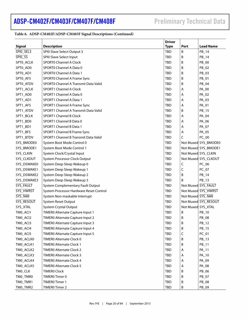
ADSP-CM402F/ADSP-CM403F SIGNAL DESCRIPTIONSTable 6 identifies each signal on the chip, describes the signal, and lists the driver type, port, and lead name.
Table 6. ADSP-CM402F/ADSP-CM403F Signal Descriptions
Signal DescriptionDriver Type Port Lead Name
ADC0_VIN00 Channel 0 Single-Ended Analog Input for ADC0 TBD Not Muxed ADC0_VIN00
ADC0_VIN01 Channel 1 Single-Ended Analog Input for ADC0 TBD Not Muxed ADC0_VIN01
ADC0_VIN02 Channel 2 Single-Ended Analog Input for ADC0 TBD Not Muxed ADC0_VIN02
ADC0_VIN03 Channel 3 Single-Ended Analog Input for ADC0 TBD Not Muxed ADC0_VIN03
ADC0_VIN04 Channel 4 Single-Ended Analog Input for ADC0 TBD Not Muxed ADC0_VIN04
ADC0_VIN05 Channel 5 Single-Ended Analog Input for ADC0 TBD Not Muxed ADC0_VIN05
ADC0_VIN06 Channel 6 Single-Ended Analog Input for ADC0 TBD Not Muxed ADC0_VIN06
ADC0_VIN07 Channel 7 Single-Ended Analog Input for ADC0 TBD Not Muxed ADC0_VIN07
ADC0_VIN08 Channel 8 Single-Ended Analog Input for ADC0 TBD Not Muxed ADC0_VIN08
ADC0_VIN09 Channel 9 Single-Ended Analog Input for ADC0 TBD Not Muxed ADC0_VIN09
ADC0_VIN10 Channel 10 Single-Ended Analog Input for ADC0 TBD Not Muxed ADC0_VIN10
ADC0_VIN11 Channel 11 Single-Ended Analog Input for ADC0 TBD Not Muxed ADC0_VIN11
ADC1_VIN00 Channel 0 Single-Ended Analog Input for ADC1 TBD Not Muxed ADC1_VIN00
ADC1_VIN01 Channel 1 Single-Ended Analog Input for ADC1 TBD Not Muxed ADC1_VIN01
ADC1_VIN02 Channel 2 Single-Ended Analog Input for ADC1 TBD Not Muxed ADC1_VIN02
ADC1_VIN03 Channel 3 Single-Ended Analog Input for ADC1 TBD Not Muxed ADC1_VIN03
ADC1_VIN04 Channel 4 Single-Ended Analog Input for ADC1 TBD Not Muxed ADC1_VIN04
ADC1_VIN05 Channel 5 Single-Ended Analog Input for ADC1 TBD Not Muxed ADC1_VIN05
ADC1_VIN06 Channel 6 Single-Ended Analog Input for ADC1 TBD Not Muxed ADC1_VIN06
ADC1_VIN07 Channel 7 Single-Ended Analog Input for ADC1 TBD Not Muxed ADC1_VIN07
ADC1_VIN08 Channel 8 Single-Ended Analog Input for ADC1 TBD Not Muxed ADC1_VIN08
ADC1_VIN09 Channel 9 Single-Ended Analog Input for ADC1 TBD Not Muxed ADC1_VIN09
ADC1_VIN10 Channel 10 Single-Ended Analog Input for ADC1 TBD Not Muxed ADC1_VIN10
ADC1_VIN11 Channel 11 Single-Ended Analog Input for ADC1 TBD Not Muxed ADC1_VIN11
BYP_A0 On-chip Analog Power Regulation Bypass Filter Node for ADC0 (see recom-mended bypass - Figure 4 on Page 6)
TBD Not Muxed BYP_A0
BYP_A1 On-chip Analog Power Regulation Bypass Filter Node for ADC1 (see recom-mended bypass - Figure 4 on Page 6)
TBD Not Muxed BYP_A1
BYP_D0 On-chip Digital Power Regulation Bypass Filter Node for Analog Subsystem (see recommended bypass - Figure 4 on Page 6)
TBD Not Muxed BYP_D0
CAN0_RX CAN0 Receive TBD B PB_15
CAN0_TX CAN0 Transmit TBD C PC_00
CAN1_RX CAN1 Receive TBD B PB_10
CAN1_TX CAN1 Transmit TBD B PB_11
CNT0_DG CNT0 Count Down and Gate TBD B PB_02
CNT0_OUTA CNT0 Output Divider A TBD B PB_13
CNT0_OUTB CNT0 Output Divider B TBD B PB_14
CNT0_UD CNT0 Count Up and Direction TBD B PB_01
CNT0_ZM CNT0 Count Zero Marker TBD B PB_00
CNT1_DG CNT1 Count Down and Gate TBD B PB_05
CNT1_UD CNT1 Count Up and Direction TBD B PB_04
CNT1_ZM CNT1 Count Zero Marker TBD B PB_03

Rev. PrE | Page 18 of 84 | September 2013
ADSP-CM402F/CM403F/CM407F/CM408F Preliminary Technical Data
DAC0_VOUT Analog Voltage Output 0 TBD Not Muxed DAC0_VOUT
DAC1_VOUT Analog Voltage Output 1 TBD Not Muxed DAC1_VOUT
GND Digital Ground TBD Not Muxed GND
GND_ANA0 Analog Ground return for VDD_ANA0 (see recommended bypass - Figure 4 on Page 6)
TBD Not Muxed GND_ANA0
GND_ANA1 Analog Ground return for VDD_ANA1 (see recommended bypass - Figure 4 on Page 6)
TBD Not Muxed GND_ANA1
GND_ANA2 Analog Ground (see recommended bypass - Figure 4 on Page 6) TBD Not Muxed GND_ANA2
GND_ANA3 Analog Ground (see recommended bypass - Figure 4 on Page 6) TBD Not Muxed GND_ANA3
GND_VREF0 Ground return for VREF0 (see recommended bypass filter- Figure 4 on Page 6) TBD Not Muxed GND_VREF0
GND_VREF1 Ground return for VREF1 (see recommended bypass filter- Figure 4 on Page 6) TBD Not Muxed GND_VREF1
JTG_TCK/SWCLK JTG Clock/Serial Wire Clock TBD Not Muxed JTG_TCK/SWCLK
JTG_TDI JTG Serial Data In TBD Not Muxed JTG_TDI
JTG_TDO/SWO JTG Serial Data Out/Serial Wire Trace Output TBD Not Muxed JTG_TDO/SWO
JTG_TMS/SWDIO JTG Mode Select/Serial Wire Debug Data I/O TBD Not Muxed JTG_TMS/SWDIO
JTG_TRST JTG Reset TBD Not Muxed JTG_TRST
PA_00 – PA_15 Port A Positions 0 – 15 TBD A PA_00 – PA_15
PB_00 – PB_15 Port B Positions 0 – 15 TBD B PB_00 – PB_15
PC_00 – PC_07 Port C Positions 0 – 7 TBD C PC_00 – PC_07
PWM0_AH PWM0 Channel A High Side TBD A PA_02
PWM0_AL PWM0 Channel A Low Side TBD A PA_03
PWM0_BH PWM0 Channel B High Side TBD A PA_04
PWM0_BL PWM0 Channel B Low Side TBD A PA_05
PWM0_CH PWM0 Channel C High Side TBD A PA_06
PWM0_CL PWM0 Channel C Low Side TBD A PA_07
PWM0_DH PWM0 Channel D High Side TBD B PB_00
PWM0_DL PWM0 Channel D Low Side TBD B PB_01
PWM0_SYNC PWM0 Sync TBD A PA_00
PWM0_TRIP0 PWM0 Shutdown Input 0 TBD A PA_01
PWM1_AH PWM1 Channel A High Side TBD A PA_12
PWM1_AL PWM1 Channel A Low Side TBD A PA_13
PWM1_BH PWM1 Channel B High Side TBD A PA_14
PWM1_BL PWM1 Channel B Low Side TBD A PA_15
PWM1_CH PWM1 Channel C High Side TBD A PA_08
PWM1_CL PWM1 Channel C Low Side TBD A PA_09
PWM1_DH PWM1 Channel D High Side TBD B PB_02
PWM1_DL PWM1 Channel D Low Side TBD B PB_03
PWM1_SYNC PWM1 Sync TBD A PA_10
PWM1_TRIP0 PWM1 Shutdown Input 0 TBD A PA_11
PWM2_AH PWM2 Channel A High Side TBD B PB_06
PWM2_AL PWM2 Channel A Low Side TBD B PB_07
PWM2_BH PWM2 Channel B High Side TBD B PB_08
PWM2_BL PWM2 Channel B Low Side TBD B PB_09
PWM2_CH PWM2 Channel C High Side TBD C PC_03
PWM2_CL PWM2 Channel C Low Side TBD C PC_04
PWM2_DH PWM2 Channel D High Side TBD C PC_05
Table 6. ADSP-CM402F/ADSP-CM403F Signal Descriptions (Continued)
Signal DescriptionDriver Type Port Lead Name

Preliminary Technical Data
Rev. PrE | Page 19 of 84 | September 2013
ADSP-CM402F/CM403F/CM407F/CM408F
PWM2_DL PWM2 Channel D Low Side TBD C PC_06
PWM2_SYNC PWM2 Sync TBD B PB_04
PWM2_TRIP0 PWM2 Shutdown Input 0 TBD B PB_05
REFCAP Output of BandGap Generator Filter Node (see recommended bypass filter - Figure 4 on Page 6)
TBD Not Muxed REFCAP
SINC0_CLK0 SINC0 Clock 0 TBD B PB_10
SINC0_CLK1 SINC0 Clock 1 TBD C PC_07
SINC0_D0 SINC0 Data 0 TBD B PB_11
SINC0_D1 SINC0 Data 1 TBD B PB_12
SINC0_D2 SINC0 Data 2 TBD B PB_13
SINC0_D3 SINC0 Data 3 TBD B PB_14
SMC0_A01 SMC0 Address 1 TBD B PB_13
SMC0_A02 SMC0 Address 2 TBD B PB_14
SMC0_A03 SMC0 Address 3 TBD B PB_15
SMC0_A04 SMC0 Address 4 TBD C PC_00
SMC0_A05 SMC0 Address 5 TBD C PC_01
SMC0_AMS0 SMC0 Memory Select 0 TBD B PB_11
SMC0_AMS2 SMC0 Memory Select 2 TBD A PA_07
SMC0_AOE SMC0 Output Enable TBD B PB_12
SMC0_ARDY SMC0 Asynchronous Ready TBD B PB_08
SMC0_ARE SMC0 Read Enable TBD B PB_09
SMC0_AWE SMC0 Write Enable TBD B PB_10
SMC0_D00 SMC0 Data 0 TBD A PA_08
SMC0_D01 SMC0 Data 1 TBD A PA_09
SMC0_D02 SMC0 Data 2 TBD A PA_10
SMC0_D03 SMC0 Data 3 TBD A PA_11
SMC0_D04 SMC0 Data 4 TBD A PA_12
SMC0_D05 SMC0 Data 5 TBD A PA_13
SMC0_D06 SMC0 Data 6 TBD A PA_14
SMC0_D07 SMC0 Data 7 TBD A PA_15
SMC0_D08 SMC0 Data 8 TBD B PB_00
SMC0_D09 SMC0 Data 9 TBD B PB_01
SMC0_D10 SMC0 Data 10 TBD B PB_02
SMC0_D11 SMC0 Data 11 TBD B PB_03
SMC0_D12 SMC0 Data 12 TBD B PB_04
SMC0_D13 SMC0 Data 13 TBD B PB_05
SMC0_D14 SMC0 Data 14 TBD B PB_06
SMC0_D15 SMC0 Data 15 TBD B PB_07
SPI0_CLK SPI0 Clock TBD C PC_03
SPI0_D2 SPI0 Data 2 TBD B PB_10
SPI0_D3 SPI0 Data 3 TBD B PB_11
SPI0_MISO SPI0 Master In, Slave Out TBD C PC_04
SPI0_MOSI SPI0 Master Out, Slave In TBD C PC_05
SPI0_RDY SPI0 Ready TBD C PC_02
SPI0_SEL1 SPI0 Slave Select Output 1 TBD C PC_06
SPI0_SEL2 SPI0 Slave Select Output 2 TBD B PB_13
Table 6. ADSP-CM402F/ADSP-CM403F Signal Descriptions (Continued)
Signal DescriptionDriver Type Port Lead Name
Rev. PrE | Page 20 of 84 | September 2013
ADSP-CM402F/CM403F/CM407F/CM408F Preliminary Technical Data
SPI0_SEL3 SPI0 Slave Select Output 3 TBD B PB_14
SPI0_SS SPI0 Slave Select Input TBD B PB_14
SPT0_ACLK SPORT0 Channel A Clock TBD B PB_00
SPT0_AD0 SPORT0 Channel A Data 0 TBD B PB_02
SPT0_AD1 SPORT0 Channel A Data 1 TBD B PB_03
SPT0_AFS SPORT0 Channel A Frame Sync TBD B PB_01
SPT0_ATDV SPORT0 Channel A Transmit Data Valid TBD B PB_04
SPT1_ACLK SPORT1 Channel A Clock TBD A PA_00
SPT1_AD0 SPORT1 Channel A Data 0 TBD A PA_02
SPT1_AD1 SPORT1 Channel A Data 1 TBD A PA_03
SPT1_AFS SPORT1 Channel A Frame Sync TBD A PA_01
SPT1_ATDV SPORT1 Channel A Transmit Data Valid TBD B PB_15
SPT1_BCLK SPORT1 Channel B Clock TBD A PA_04
SPT1_BD0 SPORT1 Channel B Data 0 TBD A PA_06
SPT1_BD1 SPORT1 Channel B Data 1 TBD A PA_07
SPT1_BFS SPORT1 Channel B Frame Sync TBD A PA_05
SPT1_BTDV SPORT1 Channel B Transmit Data Valid TBD C PC_00
SYS_BMODE0 System Boot Mode Control 0 TBD Not Muxed SYS_BMODE0
SYS_BMODE1 System Boot Mode Control 1 TBD Not Muxed SYS_BMODE1
SYS_CLKIN System Clock/Crystal Input TBD Not Muxed SYS_CLKIN
SYS_CLKOUT System Processor Clock Output TBD Not Muxed SYS_CLKOUT
SYS_DSWAKE0 System Deep Sleep Wakeup 0 TBD C PC_06
SYS_DSWAKE1 System Deep Sleep Wakeup 1 TBD C PC_07
SYS_DSWAKE2 System Deep Sleep Wakeup 2 TBD B PB_14
SYS_DSWAKE3 System Deep Sleep Wakeup 3 TBD B PB_13
SYS_FAULT System Complementary Fault Output TBD Not Muxed SYS_FAULT
SYS_HWRST System Processor Hardware Reset Control TBD Not Muxed SYS_HWRST
SYS_NMI System Non-maskable Interrupt TBD Not Muxed SYS_NMI
SYS_RESOUT System Reset Output TBD Not Muxed SYS_RESOUT
SYS_XTAL System Crystal Output TBD Not Muxed SYS_XTAL
TM0_ACI1 TIMER0 Alternate Capture Input 1 TBD B PB_10
TM0_ACI2 TIMER0 Alternate Capture Input 2 TBD B PB_08
TM0_ACI3 TIMER0 Alternate Capture Input 3 TBD B PB_12
TM0_ACI4 TIMER0 Alternate Capture Input 4 TBD B PB_15
TM0_ACI5 TIMER0 Alternate Capture Input 5 TBD C PC_01
TM0_ACLK0 TIMER0 Alternate Clock 0 TBD B PB_13
TM0_ACLK1 TIMER0 Alternate Clock 1 TBD B PB_11
TM0_ACLK2 TIMER0 Alternate Clock 2 TBD A PA_11
TM0_ACLK3 TIMER0 Alternate Clock 3 TBD A PA_10
TM0_ACLK4 TIMER0 Alternate Clock 4 TBD A PA_09
TM0_ACLK5 TIMER0 Alternate Clock 5 TBD A PA_08
TM0_CLK TIMER0 Clock TBD B PB_06
TM0_TMR0 TIMER0 Timer 0 TBD B PB_07
TM0_TMR1 TIMER0 Timer 1 TBD B PB_08
TM0_TMR2 TIMER0 Timer 2 TBD B PB_09
Table 6. ADSP-CM402F/ADSP-CM403F Signal Descriptions (Continued)
Signal DescriptionDriver Type Port Lead Name

Preliminary Technical Data
Rev. PrE | Page 21 of 84 | September 2013
ADSP-CM402F/CM403F/CM407F/CM408F
TM0_TMR3 TIMER0 Timer 3 TBD A PA_15
TM0_TMR4 TIMER0 Timer 4 TBD A PA_12
TM0_TMR5 TIMER0 Timer 5 TBD A PA_13
TM0_TMR6 TIMER0 Timer 6 TBD A PA_14
TM0_TMR7 TIMER0 Timer 7 TBD B PB_05
TRACE_CLK Embedded Trace Module Clock TBD B PB_00
TRACE_D0 Embedded Trace Module Data 0 TBD B PB_01
TRACE_D1 Embedded Trace Module Data 1 TBD B PB_02
TRACE_D2 Embedded Trace Module Data 2 TBD B PB_03
TRACE_D3 Embedded Trace Module Data 3 TBD C PC_02
TWI0_SCL TWI0 Serial Clock TBD Not Muxed TWI0_SCL
TWI0_SDA TWI0 Serial Data TBD Not Muxed TWI0_SDA
UART0_CTS UART0 Clear to Send TBD B PB_05
UART0_RTS UART0 Request to Send TBD B PB_04
UART0_RX UART0 Receive TBD C PC_01
UART0_TX UART0 Transmit TBD C PC_02
UART1_CTS UART1 Clear to Send TBD A PA_11
UART1_RTS UART1 Request to Send TBD C PC_07
UART1_RX UART1 Receive TBD B PB_08
UART1_RX UART1 Receive TBD B PB_15
UART1_TX UART1 Transmit TBD B PB_09
UART1_TX UART1 Transmit TBD C PC_00
UART2_RX UART2 Receive TBD B PB_12
UART2_TX UART2 Transmit TBD C PC_07
VDD_ANA0 Analog Power Supply Voltage (see recommended bypass - Figure 4 on Page 6) TBD Not Muxed VDD_ANA0
VDD_ANA1 Analog Power Supply Voltage (see recommended bypass - Figure 4 on Page 6) TBD Not Muxed VDD_ANA1
VDD_EXT External Voltage Domain TBD Not Muxed VDD_EXT
VDD_INT Internal Voltage Domain TBD Not Muxed VDD_INT
VDD_VREG VREG Supply Voltage TBD Not Muxed VDD_VREG
VREF0 Voltage Reference for ADC0. Default configuration is Output (see recommended bypass - Figure 4 on Page 6)
TBD Not Muxed VREF0
VREF1 Voltage Reference for ADC1. Default configuration is Output (see recommended bypass - Figure 4 on Page 6)
TBD Not Muxed VREF1
VREG_BASE Voltage Regulator Base Node TBD Not Muxed VREG_BASE
Table 6. ADSP-CM402F/ADSP-CM403F Signal Descriptions (Continued)
Signal DescriptionDriver Type Port Lead Name

Rev. PrE | Page 22 of 84 | September 2013
ADSP-CM402F/CM403F/CM407F/CM408F Preliminary Technical Data
ADSP-CM402F/ADSP-CM403F MULTIPLEXED PINSTable 7 through Table 9 identify the signals on each multiplexed pin on the chip, one table per port. The various functions are accessed through the indicated PORT_FER register and PORT_MUX register settings for each port.
Table 7. Signal Muxing Table Port A
PORT_FER = 0 PORT_FER = 1
GPIO PORT_MUX=b#00 PORT_MUX=b#01 PORT_MUX=b#10 PORT_MUX=b#11 Input Tap
PA_00 PWM0_SYNC SPT1_ACLK
PA_01 PWM0_TRIP0 SPT1_AFS
PA_02 PWM0_AH SPT1_AD0
PA_03 PWM0_AL SPT1_AD1
PA_04 PWM0_BH SPT1_BCLK
PA_05 PWM0_BL SPT1_BFS
PA_06 PWM0_CH SPT1_BD0
PA_07 PWM0_CL SMC0_AMS2 SPT1_BD1
PA_08 PWM1_CH SMC0_D00 TM0_ACLK5
PA_09 PWM1_CL SMC0_D01 TM0_ACLK4
PA_10 PWM1_SYNC SMC0_D02 TM0_ACLK3
PA_11 PWM1_TRIP0 UART1_CTS SMC0_D03 TM0_ACLK2
PA_12 PWM1_AH TM0_TMR4 SMC0_D04
PA_13 PWM1_AL TM0_TMR5 SMC0_D05
PA_14 PWM1_BH TM0_TMR6 SMC0_D06
PA_15 PWM1_BL TM0_TMR3 SMC0_D07
Table 8. Signal Muxing Table Port B
PORT_FER = 0 PORT_FER = 1
GPIO PORT_MUX=b#00 PORT_MUX=b#01 PORT_MUX=b#10 PORT_MUX=b#11 Input Tap
PB_00 PWM0_DH TRACE_CLK SPT0_ACLK SMC0_D08 CNT0_ZM
PB_01 PWM0_DL TRACE_D0 SPT0_AFS SMC0_D09 CNT0_UD
PB_02 PWM1_DH TRACE_D1 SPT0_AD0 SMC0_D10 CNT0_DG
PB_03 PWM1_DL TRACE_D2 SPT0_AD1 SMC0_D11 CNT1_ZM
PB_04 PWM2_SYNC UART0_RTS SPT0_ATDV SMC0_D12 CNT1_UD
PB_05 PWM2_TRIP0 UART0_CTS TM0_TMR7 SMC0_D13 CNT1_DG
PB_06 PWM2_AH TM0_CLK SMC0_D14
PB_07 PWM2_AL TM0_TMR0 SMC0_D15
PB_08 PWM2_BH TM0_TMR1 UART1_RX SMC0_ARDY TM0_ACI2
PB_09 PWM2_BL TM0_TMR2 UART1_TX SMC0_ARE
PB_10 SINC0_CLK0 SPI0_D2 CAN1_RX SMC0_AWE TM0_ACI1
PB_11 SINC0_D0 SPI0_D3 CAN1_TX SMC0_AMS0 TM0_ACLK1
PB_12 SINC0_D1 UART2_RX SMC0_AOE TM0_ACI3
PB_13 SINC0_D2 CNT0_OUTA SPI0_SEL2 SMC0_A01 TM0_ACLK0/SYS_DSWAKE3
PB_14 SINC0_D3 CNT0_OUTB SPI0_SEL3 SMC0_A02 SPI0_SS/SYS_DSWAKE2
PB_15 CAN0_RX SPT1_ATDV UART1_RX SMC0_A03 TM0_ACI4

Preliminary Technical Data
Rev. PrE | Page 23 of 84 | September 2013
ADSP-CM402F/CM403F/CM407F/CM408F
Table 9. Signal Muxing Table Port C
PORT_FER = 0 PORT_FER = 1
GPIO PORT_MUX=b#00 PORT_MUX=b#01 PORT_MUX=b#10 PORT_MUX=b#11 Input Tap
PC_00 CAN0_TX SPT1_BTDV UART1_TX SMC0_A04
PC_01 UART0_RX SMC0_A05 TM0_ACI5
PC_02 UART0_TX TRACE_D3 SPI0_RDY
PC_03 SPI0_CLK PWM2_CH
PC_04 SPI0_MISO PWM2_CL
PC_05 SPI0_MOSI PWM2_DH
PC_06 SPI0_SEL1 PWM2_DL SYS_DSWAKE0
PC_07 SINC0_CLK1 UART2_TX UART1_RTS SYS_DSWAKE1

Rev. PrE | Page 24 of 84 | September 2013
ADSP-CM402F/CM403F/CM407F/CM408F Preliminary Technical Data
ADSP-CM407F/ADSP-CM408F SIGNAL DESCRIPTIONSTable 10 identifies each signal on the chip, describes the signal, and lists the driver type, port, and lead name.
Table 10. ADSP-CM407F/ADSP-CM408F Signal Descriptions
Signal DescriptionDriverType Port Lead Name
ADC0_VIN00 Channel 0 Single-Ended Analog Input for ADC0 TBD Not Muxed ADC0_VIN00
ADC0_VIN01 Channel 1 Single-Ended Analog Input for ADC0 TBD Not Muxed ADC0_VIN01
ADC0_VIN02 Channel 2 Single-Ended Analog Input for ADC0 TBD Not Muxed ADC0_VIN02
ADC0_VIN03 Channel 3 Single-Ended Analog Input for ADC0 TBD Not Muxed ADC0_VIN03
ADC0_VIN04 Channel 4 Single-Ended Analog Input for ADC0 TBD Not Muxed ADC0_VIN04
ADC0_VIN05 Channel 5 Single-Ended Analog Input for ADC0 TBD Not Muxed ADC0_VIN05
ADC0_VIN06 Channel 6 Single-Ended Analog Input for ADC0 TBD Not Muxed ADC0_VIN06
ADC0_VIN07 Channel 7 Single-Ended Analog Input for ADC0 TBD Not Muxed ADC0_VIN07
ADC1_VIN00 Channel 0 Single-Ended Analog Input for ADC1 TBD Not Muxed ADC1_VIN00
ADC1_VIN01 Channel 1 Single-Ended Analog Input for ADC1 TBD Not Muxed ADC1_VIN01
ADC1_VIN02 Channel 2 Single-Ended Analog Input for ADC1 TBD Not Muxed ADC1_VIN02
ADC1_VIN03 Channel 3 Single-Ended Analog Input for ADC1 TBD Not Muxed ADC1_VIN03
ADC1_VIN04 Channel 4 Single-Ended Analog Input for ADC1 TBD Not Muxed ADC1_VIN04
ADC1_VIN05 Channel 5 Single-Ended Analog Input for ADC1 TBD Not Muxed ADC1_VIN05
ADC1_VIN06 Channel 6 Single-Ended Analog Input for ADC1 TBD Not Muxed ADC1_VIN06
ADC1_VIN07 Channel 7 Single-Ended Analog Input for ADC1 TBD Not Muxed ADC1_VIN07
BYP_A0 On-chip Analog Power Regulation Bypass Filter Node for ADC0 (see recom-mended bypass - Figure 4 on Page 6)
TBD Not Muxed BYP_A0
BYP_A1 On-chip Analog Power Regulation Bypass Filter Node for ADC1 (see recom-mended bypass - Figure 4 on Page 6)
TBD Not Muxed BYP_A1
BYP_D0 On-chip Digital Power Regulation Bypass Filter Node for Analog Subsystem (see recommended bypass - Figure 4 on Page 6)
TBD Not Muxed BYP_D0
CAN0_RX CAN0 Receive TBD B PB_15
CAN0_TX CAN0 Transmit TBD C PC_00
CAN1_RX CAN1 Receive TBD B PB_10
CAN1_TX CAN1 Transmit TBD B PB_11
CNT0_DG CNT0 Count Down and Gate TBD B PB_02
CNT0_OUTA CNT0 Output Divider A TBD B PB_13
CNT0_OUTA CNT0 Output Divider A TBD F PF_00
CNT0_OUTB CNT0 Output Divider B TBD B PB_14
CNT0_OUTB CNT0 Output Divider B TBD F PF_01
CNT0_UD CNT0 Count Up and Direction TBD B PB_01
CNT0_ZM CNT0 Count Zero Marker TBD B PB_00
CNT1_DG CNT1 Count Down and Gate TBD B PB_05
CNT1_OUTA CNT1 Output Divider A TBD E PE_14
CNT1_OUTB CNT1 Output Divider B TBD E PE_15
CNT1_UD CNT1 Count Up and Direction TBD B PB_04
CNT1_ZM CNT1 Count Zero Marker TBD B PB_03
CNT2_DG CNT2 Count Down and Gate TBD E PE_10
CNT2_UD CNT2 Count Up and Direction TBD E PE_09
CNT2_ZM CNT2 Count Zero Marker TBD E PE_08
CNT3_DG CNT3 Count Down and Gate TBD E PE_13

Preliminary Technical Data
Rev. PrE | Page 25 of 84 | September 2013
ADSP-CM402F/CM403F/CM407F/CM408F
CNT3_UD CNT3 Count Up and Direction TBD E PE_12
CNT3_ZM CNT3 Count Zero Marker TBD E PE_11
ETH0_CRS EMAC0 Carrier Sense/RMII Receive Data Valid TBD E PE_09
ETH0_MDC EMAC0 Management Channel Clock TBD E PE_11
ETH0_MDIO EMAC0 Management Channel Serial Data TBD E PE_10
ETH0_PTPAUXIN EMAC0 PTP Auxiliary Trigger Input TBD E PE_07
ETH0_PTPCLKIN EMAC0 PTP Clock Input TBD F PF_10
ETH0_PTPPPS EMAC0 PTP Pulse-Per-Second Output TBD E PE_08
ETH0_REFCLK EMAC0 Reference Clock TBD E PE_15
ETH0_RXD0 EMAC0 Receive Data 0 TBD F PF_00
ETH0_RXD1 EMAC0 Receive Data 1 TBD F PF_01
ETH0_TXD0 EMAC0 Transmit Data 0 TBD E PE_12
ETH0_TXD1 EMAC0 Transmit Data 1 TBD E PE_13
ETH0_TXEN EMAC0 Transmit Enable TBD E PE_14
GND Digital Ground TBD Not Muxed GND
GND_ANA0 Analog Ground return for VDD_ANA0 (see recommended bypass - Figure 4 on Page 6)
TBD Not Muxed GND_ANA0
GND_ANA1 Analog Ground return for VDD_ANA1 (see recommended bypass - Figure 4 on Page 6)
TBD Not Muxed GND_ANA1
GND_ANA2 Analog Ground (see recommended bypass - Figure 4 on Page 6) TBD Not Muxed GND_ANA2
GND_ANA3 Analog Ground (see recommended bypass - Figure 4 on Page 6) TBD Not Muxed GND_ANA3
GND_VREF0 Ground return for VREF0 (see recommended bypass filter- Figure 4 on Page 6)
TBD Not Muxed GND_VREF0
GND_VREF1 Ground return for VREF1 (see recommended bypass filter- Figure 4 on Page 6)
TBD Not Muxed GND_VREF1
JTG_TCK/SWCLK JTG Clock/Serial Wire Clock TBD Not Muxed JTG_TCK/SWCLK
JTG_TDI JTG Serial Data In TBD Not Muxed JTG_TDI
JTG_TDO/SWO JTG Serial Data Out/Serial Wire Trace Output TBD Not Muxed JTG_TDO/SWO
JTG_TMS/SWDIO JTG Mode Select/Serial Wire Debug Data I/O TBD Not Muxed JTG_TMS/SWDIO
JTG_TRST JTG Reset TBD Not Muxed JTG_TRST
PA_00 – PA_15 Port A Positions 0 – 15 TBD A PA_00 – PA_15
PB_00 – PB_15 Port B Positions 0 – 15 TBD B PB_00 – PB_15
PC_00 – PC_15 Port C Positions 0 – 15 TBD C PC_00 – PC_15
PD_00 – PD_15 Port D Positions 0 – 15 TBD D PD_00 – PD_15
PE_00 – PE_15 Port E Positions 0 – 15 TBD E PE_00 – PE_15
PF_00 – PF_10 Port F Positions 0 – 10 TBD F PF_00 – PF_10
PWM0_AH PWM0 Channel A High Side TBD A PA_02
PWM0_AL PWM0 Channel A Low Side TBD A PA_03
PWM0_BH PWM0 Channel B High Side TBD A PA_04
PWM0_BL PWM0 Channel B Low Side TBD A PA_05
PWM0_CH PWM0 Channel C High Side TBD A PA_06
PWM0_CL PWM0 Channel C Low Side TBD A PA_07
PWM0_DH PWM0 Channel D High Side TBD B PB_00
PWM0_DL PWM0 Channel D Low Side TBD B PB_01
PWM0_SYNC PWM0 Sync TBD A PA_00
PWM0_TRIP0 PWM0 Shutdown Input 0 TBD A PA_01
Table 10. ADSP-CM407F/ADSP-CM408F Signal Descriptions (Continued)
Signal DescriptionDriverType Port Lead Name

Rev. PrE | Page 26 of 84 | September 2013
ADSP-CM402F/CM403F/CM407F/CM408F Preliminary Technical Data
PWM1_AH PWM1 Channel A High Side TBD A PA_12
PWM1_AL PWM1 Channel A Low Side TBD A PA_13
PWM1_BH PWM1 Channel B High Side TBD A PA_14
PWM1_BL PWM1 Channel B Low Side TBD A PA_15
PWM1_CH PWM1 Channel C High Side TBD A PA_08
PWM1_CL PWM1 Channel C Low Side TBD A PA_09
PWM1_DH PWM1 Channel D High Side TBD B PB_02
PWM1_DL PWM1 Channel D Low Side TBD B PB_03
PWM1_SYNC PWM1 Sync TBD A PA_10
PWM1_TRIP0 PWM1 Shutdown Input 0 TBD A PA_11
PWM2_AH PWM2 Channel A High Side TBD B PB_06
PWM2_AL PWM2 Channel A Low Side TBD B PB_07
PWM2_BH PWM2 Channel B High Side TBD B PB_08
PWM2_BL PWM2 Channel B Low Side TBD B PB_09
PWM2_CH PWM2 Channel C High Side TBD C PC_03
PWM2_CL PWM2 Channel C Low Side TBD C PC_04
PWM2_DH PWM2 Channel D High Side TBD C PC_05
PWM2_DL PWM2 Channel D Low Side TBD C PC_06
PWM2_SYNC PWM2 Sync TBD B PB_04
PWM2_TRIP0 PWM2 Shutdown Input 0 TBD B PB_05
REFCAP Output of BandGap Generator Filter Node (see recommended bypass filter - Figure 4 on Page 6)
TBD Not Muxed REFCAP
SINC0_CLK0 SINC0 Clock 0 TBD B PB_10
SINC0_CLK1 SINC0 Clock 1 TBD C PC_07
SINC0_D0 SINC0 Data 0 TBD B PB_11
SINC0_D1 SINC0 Data 1 TBD B PB_12
SINC0_D2 SINC0 Data 2 TBD B PB_13
SINC0_D3 SINC0 Data 3 TBD B PB_14
SMC0_A01 SMC0 Address 1 TBD B PB_13
SMC0_A01 SMC0 Address 1 TBD F PF_05
SMC0_A02 SMC0 Address 2 TBD B PB_14
SMC0_A02 SMC0 Address 2 TBD F PF_06
SMC0_A03 SMC0 Address 3 TBD B PB_15
SMC0_A03 SMC0 Address 3 TBD F PF_07
SMC0_A04 SMC0 Address 4 TBD C PC_00
SMC0_A04 SMC0 Address 4 TBD F PF_08
SMC0_A05 SMC0 Address 5 TBD C PC_01
SMC0_A05 SMC0 Address 5 TBD F PF_09
SMC0_A06 SMC0 Address 6 TBD D PD_08
SMC0_A07 SMC0 Address 7 TBD D PD_09
SMC0_A08 SMC0 Address 8 TBD D PD_10
SMC0_A09 SMC0 Address 9 TBD D PD_11
SMC0_A10 SMC0 Address 10 TBD D PD_12
SMC0_A11 SMC0 Address 11 TBD D PD_13
SMC0_A12 SMC0 Address 12 TBD D PD_14
SMC0_A13 SMC0 Address 13 TBD D PD_15
Table 10. ADSP-CM407F/ADSP-CM408F Signal Descriptions (Continued)
Signal DescriptionDriverType Port Lead Name

Preliminary Technical Data
Rev. PrE | Page 27 of 84 | September 2013
ADSP-CM402F/CM403F/CM407F/CM408F
SMC0_A14 SMC0 Address 14 TBD E PE_00
SMC0_A15 SMC0 Address 15 TBD E PE_01
SMC0_A16 SMC0 Address 16 TBD E PE_02
SMC0_A17 SMC0 Address 17 TBD E PE_03
SMC0_A18 SMC0 Address 18 TBD E PE_04
SMC0_A19 SMC0 Address 19 TBD E PE_05
SMC0_A20 SMC0 Address 20 TBD E PE_06
SMC0_A21 SMC0 Address 21 TBD E PE_07
SMC0_A22 SMC0 Address 22 TBD E PE_08
SMC0_A23 SMC0 Address 23 TBD E PE_09
SMC0_A24 SMC0 Address 24 TBD E PE_11
SMC0_ABE0 SMC0 Byte Enable 0 TBD E PE_12
SMC0_ABE1 SMC0 Byte Enable 1 TBD E PE_13
SMC0_AMS0 SMC0 Memory Select 0 TBD B PB_11
SMC0_AMS0 SMC0 Memory Select 0 TBD Not Muxed SMC0_AMS0
SMC0_AMS1 SMC0 Memory Select 1 TBD E PE_10
SMC0_AMS2 SMC0 Memory Select 2 TBD A PA_07
SMC0_AMS3 SMC0 Memory Select 3 TBD C PC_11
SMC0_AOE SMC0 Output Enable TBD B PB_12
SMC0_AOE SMC0 Output Enable TBD F PF_03
SMC0_ARDY SMC0 Asynchronous Ready TBD B PB_08
SMC0_ARDY SMC0 Asynchronous Ready TBD F PF_04
SMC0_ARE SMC0 Read Enable TBD B PB_09
SMC0_ARE SMC0 Read Enable TBD Not Muxed SMC0_ARE
SMC0_AWE SMC0 Write Enable TBD B PB_10
SMC0_AWE SMC0 Write Enable TBD Not Muxed SMC0_AWE
SMC0_D00 SMC0 Data 0 TBD A PA_08
SMC0_D00 SMC0 Data 0 TBD C PC_08
SMC0_D01 SMC0 Data 1 TBD A PA_09
SMC0_D01 SMC0 Data 1 TBD C PC_09
SMC0_D02 SMC0 Data 2 TBD A PA_10
SMC0_D02 SMC0 Data 2 TBD C PC_10
SMC0_D03 SMC0 Data 3 TBD A PA_11
SMC0_D03 SMC0 Data 3 TBD C PC_11
SMC0_D04 SMC0 Data 4 TBD A PA_12
SMC0_D04 SMC0 Data 4 TBD C PC_12
SMC0_D05 SMC0 Data 5 TBD A PA_13
SMC0_D05 SMC0 Data 5 TBD C PC_13
SMC0_D06 SMC0 Data 6 TBD A PA_14
SMC0_D06 SMC0 Data 6 TBD C PC_14
SMC0_D07 SMC0 Data 7 TBD A PA_15
SMC0_D07 SMC0 Data 7 TBD C PC_15
SMC0_D08 SMC0 Data 8 TBD B PB_00
SMC0_D08 SMC0 Data 8 TBD D PD_00
SMC0_D09 SMC0 Data 9 TBD B PB_01
Table 10. ADSP-CM407F/ADSP-CM408F Signal Descriptions (Continued)
Signal DescriptionDriverType Port Lead Name

Rev. PrE | Page 28 of 84 | September 2013
ADSP-CM402F/CM403F/CM407F/CM408F Preliminary Technical Data
SMC0_D09 SMC0 Data 9 TBD D PD_01
SMC0_D10 SMC0 Data 10 TBD B PB_02
SMC0_D10 SMC0 Data 10 TBD D PD_02
SMC0_D11 SMC0 Data 11 TBD B PB_03
SMC0_D11 SMC0 Data 11 TBD D PD_03
SMC0_D12 SMC0 Data 12 TBD B PB_04
SMC0_D12 SMC0 Data 12 TBD D PD_04
SMC0_D13 SMC0 Data 13 TBD B PB_05
SMC0_D13 SMC0 Data 13 TBD D PD_05
SMC0_D14 SMC0 Data 14 TBD B PB_06
SMC0_D14 SMC0 Data 14 TBD D PD_06
SMC0_D15 SMC0 Data 15 TBD B PB_07
SMC0_D15 SMC0 Data 15 TBD D PD_07
SPI0_CLK SPI0 Clock TBD C PC_03
SPI0_D2 SPI0 Data 2 TBD B PB_10
SPI0_D3 SPI0 Data 3 TBD B PB_11
SPI0_MISO SPI0 Master In, Slave Out TBD C PC_04
SPI0_MOSI SPI0 Master Out, Slave In TBD C PC_05
SPI0_RDY SPI0 Ready TBD C PC_02
SPI0_SEL1 SPI0 Slave Select Output 1 TBD C PC_06
SPI0_SEL2 SPI0 Slave Select Output 2 TBD B PB_13
SPI0_SEL3 SPI0 Slave Select Output 3 TBD B PB_14
SPI0_SS SPI0 Slave Select Input TBD B PB_14
SPI1_CLK SPI1 Clock TBD C PC_12
SPI1_MISO SPI1 Master In, Slave Out TBD C PC_13
SPI1_MOSI SPI1 Master Out, Slave In TBD C PC_14
SPI1_SEL1 SPI1 Slave Select Output 1 TBD C PC_15
SPI1_SEL2 SPI1 Slave Select Output 2 TBD B PB_06
SPI1_SEL3 SPI1 Slave Select Output 3 TBD B PB_07
SPI1_SS SPI1 Slave Select Input TBD C PC_15
SPT0_ACLK SPORT0 Channel A Clock TBD B PB_00
SPT0_AD0 SPORT0 Channel A Data 0 TBD B PB_02
SPT0_AD1 SPORT0 Channel A Data 1 TBD B PB_03
SPT0_AFS SPORT0 Channel A Frame Sync TBD B PB_01
SPT0_ATDV SPORT0 Channel A Transmit Data Valid TBD B PB_04
SPT0_BCLK SPORT0 Channel B Clock TBD C PC_08
SPT0_BD0 SPORT0 Channel B Data 0 TBD C PC_10
SPT0_BD1 SPORT0 Channel B Data 1 TBD C PC_11
SPT0_BFS SPORT0 Channel B Frame Sync TBD C PC_09
SPT0_BTDV SPORT0 Channel B Transmit Data Valid TBD B PB_12
SPT1_ACLK SPORT1 Channel A Clock TBD A PA_00
SPT1_AD0 SPORT1 Channel A Data 0 TBD A PA_02
SPT1_AD1 SPORT1 Channel A Data 1 TBD A PA_03
SPT1_AFS SPORT1 Channel A Frame Sync TBD A PA_01
SPT1_ATDV SPORT1 Channel A Transmit Data Valid TBD B PB_15
Table 10. ADSP-CM407F/ADSP-CM408F Signal Descriptions (Continued)
Signal DescriptionDriverType Port Lead Name

Preliminary Technical Data
Rev. PrE | Page 29 of 84 | September 2013
ADSP-CM402F/CM403F/CM407F/CM408F
SPT1_BCLK SPORT1 Channel B Clock TBD A PA_04
SPT1_BD0 SPORT1 Channel B Data 0 TBD A PA_06
SPT1_BD1 SPORT1 Channel B Data 1 TBD A PA_07
SPT1_BFS SPORT1 Channel B Frame Sync TBD A PA_05
SPT1_BTDV SPORT1 Channel B Transmit Data Valid TBD C PC_00
SYS_BMODE0 System Boot Mode Control 0 TBD Not Muxed SYS_BMODE0
SYS_BMODE1 System Boot Mode Control 1 TBD Not Muxed SYS_BMODE1
SYS_CLKIN System Clock/Crystal Input TBD Not Muxed SYS_CLKIN
SYS_CLKOUT System Processor Clock Output TBD Not Muxed SYS_CLKOUT
SYS_DSWAKE0 System Deep Sleep Wakeup 0 TBD C PC_06
SYS_DSWAKE1 System Deep Sleep Wakeup 1 TBD C PC_07
SYS_DSWAKE2 System Deep Sleep Wakeup 2 TBD B PB_14
SYS_DSWAKE3 System Deep Sleep Wakeup 3 TBD B PB_13
SYS_FAULT System Complementary Fault Output TBD Not Muxed SYS_FAULT
SYS_HWRST System Processor Hardware Reset Control TBD Not Muxed SYS_HWRST
SYS_NMI System Non-maskable Interrupt TBD Not Muxed SYS_NMI
SYS_RESOUT System Reset Output TBD Not Muxed SYS_RESOUT
SYS_XTAL System Crystal Output TBD Not Muxed SYS_XTAL
TM0_ACI1 TIMER0 Alternate Capture Input 1 TBD B PB_10
TM0_ACI2 TIMER0 Alternate Capture Input 2 TBD B PB_08
TM0_ACI3 TIMER0 Alternate Capture Input 3 TBD B PB_12
TM0_ACI4 TIMER0 Alternate Capture Input 4 TBD B PB_15
TM0_ACI5 TIMER0 Alternate Capture Input 5 TBD C PC_01
TM0_ACLK0 TIMER0 Alternate Clock 0 TBD B PB_13
TM0_ACLK1 TIMER0 Alternate Clock 1 TBD B PB_11
TM0_ACLK2 TIMER0 Alternate Clock 2 TBD A PA_11
TM0_ACLK3 TIMER0 Alternate Clock 3 TBD A PA_10
TM0_ACLK4 TIMER0 Alternate Clock 4 TBD A PA_09
TM0_ACLK5 TIMER0 Alternate Clock 5 TBD A PA_08
TM0_CLK TIMER0 Clock TBD B PB_06
TM0_TMR0 TIMER0 Timer 0 TBD B PB_07
TM0_TMR1 TIMER0 Timer 1 TBD B PB_08
TM0_TMR2 TIMER0 Timer 2 TBD B PB_09
TM0_TMR3 TIMER0 Timer 3 TBD A PA_15
TM0_TMR4 TIMER0 Timer 4 TBD A PA_12
TM0_TMR5 TIMER0 Timer 5 TBD A PA_13
TM0_TMR6 TIMER0 Timer 6 TBD A PA_14
TM0_TMR7 TIMER0 Timer 7 TBD B PB_05
TRACE_CLK Clock TBD B PB_00
TRACE_D0 Embedded Trace Module Data 0 TBD B PB_01
TRACE_D1 Embedded Trace Module Data 1 TBD B PB_02
TRACE_D2 Embedded Trace Module Data 2 TBD B PB_03
TRACE_D3 Embedded Trace Module Data 3 TBD C PC_02
TRACE_D3 Embedded Trace Module Data 3 TBD F PF_02
TWI0_SCL TWI0 Serial Clock TBD Not Muxed TWI0_SCL
Table 10. ADSP-CM407F/ADSP-CM408F Signal Descriptions (Continued)
Signal DescriptionDriverType Port Lead Name
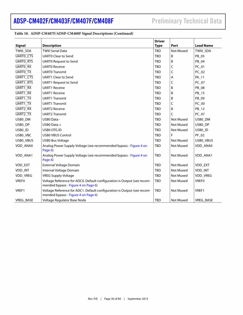
Rev. PrE | Page 30 of 84 | September 2013
ADSP-CM402F/CM403F/CM407F/CM408F Preliminary Technical Data
TWI0_SDA TWI0 Serial Data TBD Not Muxed TWI0_SDA
UART0_CTS UART0 Clear to Send TBD B PB_05
UART0_RTS UART0 Request to Send TBD B PB_04
UART0_RX UART0 Receive TBD C PC_01
UART0_TX UART0 Transmit TBD C PC_02
UART1_CTS UART1 Clear to Send TBD A PA_11
UART1_RTS UART1 Request to Send TBD C PC_07
UART1_RX UART1 Receive TBD B PB_08
UART1_RX UART1 Receive TBD B PB_15
UART1_TX UART1 Transmit TBD B PB_09
UART1_TX UART1 Transmit TBD C PC_00
UART2_RX UART2 Receive TBD B PB_12
UART2_TX UART2 Transmit TBD C PC_07
USB0_DM USB0 Data - TBD Not Muxed USB0_DM
USB0_DP USB0 Data + TBD Not Muxed USB0_DP
USB0_ID USB0 OTG ID TBD Not Muxed USB0_ID
USB0_VBC USB0 VBUS Control TBD F PF_02
USB0_VBUS USB0 Bus Voltage TBD Not Muxed USB0_VBUS
VDD_ANA0 Analog Power Supply Voltage (see recommended bypass - Figure 4 on Page 6)
TBD Not Muxed VDD_ANA0
VDD_ANA1 Analog Power Supply Voltage (see recommended bypass - Figure 4 on Page 6)
TBD Not Muxed VDD_ANA1
VDD_EXT External Voltage Domain TBD Not Muxed VDD_EXT
VDD_INT Internal Voltage Domain TBD Not Muxed VDD_INT
VDD_VREG VREG Supply Voltage TBD Not Muxed VDD_VREG
VREF0 Voltage Reference for ADC0. Default configuration is Output (see recom-mended bypass - Figure 4 on Page 6)
TBD Not Muxed VREF0
VREF1 Voltage Reference for ADC1. Default configuration is Output (see recom-mended bypass - Figure 4 on Page 6)
TBD Not Muxed VREF1
VREG_BASE Voltage Regulator Base Node TBD Not Muxed VREG_BASE
Table 10. ADSP-CM407F/ADSP-CM408F Signal Descriptions (Continued)
Signal DescriptionDriverType Port Lead Name

Preliminary Technical Data
Rev. PrE | Page 31 of 84 | September 2013
ADSP-CM402F/CM403F/CM407F/CM408F
ADSP-CM407F/ADSP-CM408F MULTIPLEXED PINSTable 11 through Table 16 identify the signals on each multi-plexed pin on the chip, one table per port. The various functions are accessed through the indicated PORT_FER register and PORT_MUX register settings for each port.
Table 11. Signal Muxing Table Port A
PORT_FER = 0 PORT_FER = 1
GPIO PORT_MUX=b#00 PORT_MUX=b#01 PORT_MUX=b#10 PORT_MUX=b#11 Input Tap
PA_00 PWM0_SYNC SPT1_ACLK
PA_01 PWM0_TRIP0 SPT1_AFS
PA_02 PWM0_AH SPT1_AD0
PA_03 PWM0_AL SPT1_AD1
PA_04 PWM0_BH SPT1_BCLK
PA_05 PWM0_BL SPT1_BFS
PA_06 PWM0_CH SPT1_BD0
PA_07 PWM0_CL SMC0_AMS2 SPT1_BD1
PA_08 PWM1_CH SMC0_D00 TM0_ACLK5
PA_09 PWM1_CL SMC0_D01 TM0_ACLK4
PA_10 PWM1_SYNC SMC0_D02 TM0_ACLK3
PA_11 PWM1_TRIP0 UART1_CTS SMC0_D03 TM0_ACLK2
PA_12 PWM1_AH TM0_TMR4 SMC0_D04
PA_13 PWM1_AL TM0_TMR5 SMC0_D05
PA_14 PWM1_BH TM0_TMR6 SMC0_D06
PA_15 PWM1_BL TM0_TMR3 SMC0_D07
Table 12. Signal Muxing Table Port B
PORT_FER = 0 PORT_FER = 1
GPIO PORT_MUX=b#00 PORT_MUX=b#01 PORT_MUX=b#10 PORT_MUX=b#11 Input Tap
PB_00 PWM0_DH TRACE_CLK SPT0_ACLK SMC0_D08 CNT0_ZM
PB_01 PWM0_DL TRACE_D0 SPT0_AFS SMC0_D09 CNT0_UD
PB_02 PWM1_DH TRACE_D1 SPT0_AD0 SMC0_D10 CNT0_DG
PB_03 PWM1_DL TRACE_D2 SPT0_AD1 SMC0_D11 CNT1_ZM
PB_04 PWM2_SYNC UART0_RTS SPT0_ATDV SMC0_D12 CNT1_UD
PB_05 PWM2_TRIP0 UART0_CTS TM0_TMR7 SMC0_D13 CNT1_DG
PB_06 PWM2_AH TM0_CLK SPI1_SEL2 SMC0_D14
PB_07 PWM2_AL TM0_TMR0 SPI1_SEL3 SMC0_D15
PB_08 PWM2_BH TM0_TMR1 UART1_RX SMC0_ARDY TM0_ACI2
PB_09 PWM2_BL TM0_TMR2 UART1_TX SMC0_ARE
PB_10 SINC0_CLK0 SPI0_D2 CAN1_RX SMC0_AWE TM0_ACI1
PB_11 SINC0_D0 SPI0_D3 CAN1_TX SMC0_AMS0 TM0_ACLK1
PB_12 SINC0_D1 SPT0_BTDV UART2_RX SMC0_AOE TM0_ACI3
PB_13 SINC0_D2 CNT0_OUTA SPI0_SEL2 SMC0_A01 TM0_ACLK0/SYS_DSWAKE3
PB_14 SINC0_D3 CNT0_OUTB SPI0_SEL3 SMC0_A02 SPI0_SS/SYS_DSWAKE2
PB_15 CAN0_RX SPT1_ATDV UART1_RX SMC0_A03 TM0_ACI4

Rev. PrE | Page 32 of 84 | September 2013
ADSP-CM402F/CM403F/CM407F/CM408F Preliminary Technical Data
Table 13. Signal Muxing Table Port C
PORT_FER = 0 PORT_FER = 1
GPIO PORT_MUX=b#00 PORT_MUX=b#01 PORT_MUX=b#10 PORT_MUX=b#11 Input Tap
PC_00 CAN0_TX SPT1_BTDV UART1_TX SMC0_A04
PC_01 UART0_RX SMC0_A05 TM0_ACI5
PC_02 UART0_TX TRACE_D3 SPI0_RDY
PC_03 SPI0_CLK PWM2_CH
PC_04 SPI0_MISO PWM2_CL
PC_05 SPI0_MOSI PWM2_DH
PC_06 SPI0_SEL1 PWM2_DL SYS_DSWAKE0
PC_07 SINC0_CLK1 UART2_TX UART1_RTS SYS_DSWAKE1
PC_08 SPT0_BCLK SMC0_D00
PC_09 SPT0_BFS SMC0_D01
PC_10 SPT0_BD0 SMC0_D02
PC_11 SMC0_AMS3 SPT0_BD1 SMC0_D03
PC_12 SPI1_CLK SMC0_D04
PC_13 SPI1_MISO SMC0_D05
PC_14 SPI1_MOSI SMC0_D06
PC_15 SPI1_SEL1 SMC0_D07 SPI1_SS
Table 14. Signal Muxing Table Port D
PORT_FER = 0 PORT_FER = 1
GPIO PORT_MUX=b#00 PORT_MUX=b#01 PORT_MUX=b#10 PORT_MUX=b#11 Input Tap
PD_00 SMC0_D08
PD_01 SMC0_D09
PD_02 SMC0_D10
PD_03 SMC0_D11
PD_04 SMC0_D12
PD_05 SMC0_D13
PD_06 SMC0_D14
PD_07 SMC0_D15
PD_08 SMC0_A06
PD_09 SMC0_A07
PD_10 SMC0_A08
PD_11 SMC0_A09
PD_12 SMC0_A10
PD_13 SMC0_A11
PD_14 SMC0_A12
PD_15 SMC0_A13

Preliminary Technical Data
Rev. PrE | Page 33 of 84 | September 2013
ADSP-CM402F/CM403F/CM407F/CM408F
Table 15. Signal Muxing Table Port E
PORT_FER = 0 PORT_FER = 1
GPIO PORT_MUX=b#00 PORT_MUX=b#01 PORT_MUX=b#10 PORT_MUX=b#11 Input Tap
PE_00 SMC0_A14
PE_01 SMC0_A15
PE_02 SMC0_A16
PE_03 SMC0_A17
PE_04 SMC0_A18
PE_05 SMC0_A19
PE_06 SMC0_A20
PE_07 ETH0_PTPAUXIN SMC0_A21
PE_08 ETH0_PTPPPS SMC0_A22 CNT2_ZM
PE_09 ETH0_CRS SMC0_A23 CNT2_UD
PE_10 ETH0_MDIO SMC0_AMS1 CNT2_DG
PE_11 ETH0_MDC SMC0_A24 CNT3_ZM
PE_12 ETH0_TXD0 SMC0_ABE0 CNT3_UD
PE_13 ETH0_TXD1 SMC0_ABE1 CNT3_DG
PE_14 ETH0_TXEN CNT1_OUTA
PE_15 ETH0_REFCLK CNT1_OUTB
Table 16. Signal Muxing Table Port F
PORT_FER = 0 PORT_FER = 1
GPIO PORT_MUX=b#00 PORT_MUX=b#01 PORT_MUX=b#10 PORT_MUX=b#11 Input Tap
PF_00 ETH0_RXD0 CNT0_OUTA
PF_01 ETH0_RXD1 CNT0_OUTB
PF_02 USB0_VBC TRACE_D3
PF_03 SMC0_AOE
PF_04 SMC0_ARDY
PF_05 SMC0_A01
PF_06 SMC0_A02
PF_07 SMC0_A03
PF_08 SMC0_A04
PF_09 SMC0_A05
PF_10 ETH0_PTPCLKIN

Rev. PrE | Page 34 of 84 | September 2013
ADSP-CM402F/CM403F/CM407F/CM408F Preliminary Technical Data
SPECIFICATIONSFor information about product specifications please contact your ADI representative.
OPERATING CONDITIONS
Clock Related Operating Conditions
Table 17 describes the core clock timing requirements. The data presented in the tables applies to all speed grades except where expressly noted. Figure 8 provides a graphical representation of the various clocks and their available divider values.
Parameter Conditions Min Nominal Max Unit
VDD_INT1
1 The expected nominal value is 1.2 V 5%, and initial customer designs should design with a programmable regulator that can be adjusted from 1.0 V to 1.4 V in 50 mV steps.
Digital Internal Supply Voltage TBD MHz TBD TBD TBD V
VDD_EXT2
2 Must remain powered (even if the associated function is not used).
Digital External Supply Voltage 3.13 3.3 3.47 V
VDD_ANA2 Analog Supply Voltage 3.13 3.3 3.47 V
VIH3
3 Parameter value applies to all input and bidirectional signals except TWI signals and USB0 signals.
High Level Input Voltage VDD_EXT = 3.47 V 2.0 V
VIHTWI4
4 Parameter applies to TWI_SDA and TWI_SCL.
High Level Input Voltage VDD_EXT = 3.47 V 0.7 × VVBUSTWI VVBUSTWI V
VIL3 Low Level Input Voltage VDD_EXT = 3.13 V 0.8 V
VILTWI4 Low Level Input Voltage VDD_EXT = 3.13 V 0.3 × VVBUSTWI V
TJ Junction Temperature TAMBIENT = TBD°C to +TBD°C –40 105 °C
Table 17. Clock Operating Conditions
Parameter Maximum Unit
fCCLK Core Clock Frequency (CCLK ≥ SYSCLK, CSEL ≤ SYSSEL) TBD MHz
fSYSCLK SYSCLK Frequency TBD MHz
fOCLK Output Clock Frequency TBD MHz
Table 18. Phase-Locked Loop Operating Conditions
Parameter Minimum Maximum Unit
fPLLCLK PLL Clock Frequency TBD TBD MHz
Figure 8. Clock Relationships and Divider Values
SYS_CLKIN PLL
DCLK (= USBCLK)
SYSCLK (= SCLK)
CCLKCSEL(1-31)
SSEL(1-31)
DSEL(1-31)
OCLKOSEL(1-127)
PLLCLK

Preliminary Technical Data
Rev. PrE | Page 35 of 84 | September 2013
ADSP-CM402F/CM403F/CM407F/CM408F
ELECTRICAL CHARACTERISTICS
Total Power Dissipation
Total power dissipation has two components:1. Static, including leakage current2. Dynamic, due to transistor switching characteristics
Many operating conditions can also affect power dissipation, including temperature, voltage, operating frequency, and pro-cessor activity. Electrical Characteristics on Page 35 shows the current dissipation for internal circuitry (VDD_INT). IDD_DEEPSLEEP specifies static power dissipation as a function of voltage (VDD_INT) and temperature, and IDD_INT specifies the total power specification for the listed test conditions, including the dynamic component as a function of voltage (VDD_INT) and frequency. There are two parts to the dynamic component. The first part is due to transistor switching in the core clock (CCLK) domain. This part is subject to an Activity Scaling Factor (ASF) which represents application code running on the processor core and L1 memories.
The ASF is combined with the CCLK frequency and VDD_INT dependent data in Table TBD to calculate this part. The second part is due to transistor switching in the system clock (SYSCLK) domain, which is included in the IDD_INT specification equation (TBD).
Parameter Test Conditions Min Typical Max Unit
VOH High Level Output Voltage VDD_EXT = 3.13 V, IOH = –0.5 mA 2.4 V
VOL Low Level Output Voltage VDD_EXT = 3.13 V, IOL = 2.0 mA 0.4 V
VOLTWI1
1 Applies to bidirectional pins TWI_SCL and TWI_SDA.
Low Level Output Voltage VDD_EXT = 3.13 V, IOL = 2.0 mA TBD V
IIH2
2 Applies to input pins.
High Level Input Current VDD_EXT =3.47 V, VIN = 3.47 V 10 μA
IIL2 Low Level Input Current VDD_EXT =3.47 V, VIN = 0 V 10 μA
IIHP3
3 Applies to JTAG input pins (JTG_TCK, JTG_TDI, JTG_TMS, JTG_TRST).
High Level Input Current JTAG VDD_EXT = 3.47 V, VIN = 3.47 V 100 μA
IOZH4
4 Applies to three-statable pins.
Three-State Leakage Current VDD_EXT = 3.47 V, VIN = 3.47 V 10 μA
IOZHTWI1 Three-State Leakage Current VDD_EXT =3.47 V, VIN = TBD V TBD μA
IOZL4 Three-State Leakage Current VDD_EXT = 3.47 V, VIN = 0 V 10 μA
CIN5, 6
5 Guaranteed, but not tested.6 Applies to all signal pins.
Input Capacitance fIN = 1 MHz, TJ = 25°C, VIN = 3.3 V TBD TBD pF
IDD_DEEPSLEEP7
7 See the ADSP-CM40x Mixed-Signal Control Processor with ARM Cortex-M4 Hardware Reference for definition of deep sleep operating mode.
VDD_INT Current in Deep Sleep Mode VDD_INT = TBD V, fCCLK = 0 MHz, fSYSCLK = 0 MHz, TJ = 25°C, ASF = 0.00
TBD mA
IDD_IDLE VDD_INT Current in Idle VDD_INT = TBD V, fCCLK = TBD MHz, TJ = 25°C, ASF = TBD
TBD mA
IDD_TYP VDD_INT Current VDD_INT = TBD V, fCCLK = TBD MHz, Tj = 25°C, ASF = 1.00
TBD mA
IDD_DEEPSLEEP VDD_INT Current in Deep Sleep Mode fCCLK = 0 MHz, fSYSCLK = 0 MHz TBD mA
IDD_INT VDD_INT Current fCCLK 0 MHz, fSYSCLK 0 MHz TBD mA

Rev. PrE | Page 36 of 84 | September 2013
ADSP-CM402F/CM403F/CM407F/CM408F Preliminary Technical Data
ADC/DAC SPECIFICATIONS
ADC Specifications
Typical values assume VDD_ANA = 3.3 V, VREF = 2.5 V, TJUNCTION = 25°C unless otherwise noted.
Parameter Min Typ Max Unit Test Conditions/Comment
ANALOG INPUT ADC0_VIN, 00–11, ADC1_VIN, 00–11
Requirement
Single-Ended Input Voltage Range 0 2.5 V
Characteristic
DC Leakage Current TBD μA
Input Resistance TBD ohms Figure 5 on Page 6
Input Capacitance TBD pF Condition 1= Track, Figure 5 on Page 6
TBD pF Condition 2 = Hold, Figure 5 on Page 6
VOLTAGE REFERENCE (OUTPUT MODE)
VREF0, VREF1
Characteristic
Output Voltage 2.5 ±1.25mV V
Long-Term Stability TBD ppm
Output Voltage Thermal Hysteresis TBD ppm
Output Impedance TBD ohms
Temperature Coefficient TBD ppm/°C –40°C to +105°C
VOLTAGE REFERENCE (INPUT MODE) VREF0, VREF1
Requirement
Input Voltage Range 0 2.5 V
DC Leakage Current TBD μA
Input Capacitance TBD pF
STATIC PERFORMANCE
DC ACCURACY ADC0_VIN, 00–11, ADC1_VIN, 00–11
Characteristic
Resolution 16 Bits No missing codes, natural binary coding
ADSP-CM403F/ADSP-CM408F
Differential Non-Linearity (DNL) –0.90/+1.5 LSB Figure 9 on Page 39
Integral Non-Linearity (INL) TBD ±3.5 TBD LSB Figure 12 on Page 39
Offset Error ±TBD TBD LSB
Offset Error Match TBD LSB
Offset Drift TBD LSB
Gain Error TBD LSB
Gain Error Match TBD LSB
ADSP-CM402F/ADSP-CM407F
Differential Non-Linearity (DNL) –1.0/+2.0 LSB Figure 9 on Page 39
Integral Non-Linearity (INL) TBD ±12.0 TBD LSB Figure 12 on Page 39
Offset Error ±TBD TBD LSB
Offset Error Match TBD LSB
Offset Drift TBD LSB
Gain Error TBD LSB
Gain Error Match TBD LSB
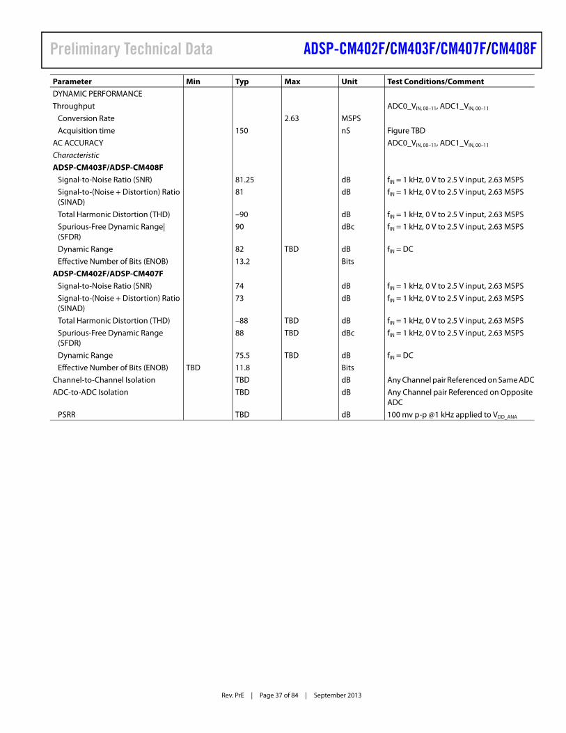
Preliminary Technical Data
Rev. PrE | Page 37 of 84 | September 2013
ADSP-CM402F/CM403F/CM407F/CM408F
DYNAMIC PERFORMANCE
Throughput ADC0_VIN, 00–11, ADC1_VIN, 00–11
Conversion Rate 2.63 MSPS
Acquisition time 150 nS Figure TBD
AC ACCURACY ADC0_VIN, 00–11, ADC1_VIN, 00–11
Characteristic
ADSP-CM403F/ADSP-CM408F
Signal-to-Noise Ratio (SNR) 81.25 dB fIN = 1 kHz, 0 V to 2.5 V input, 2.63 MSPS
Signal-to-(Noise + Distortion) Ratio (SINAD)
81 dB fIN = 1 kHz, 0 V to 2.5 V input, 2.63 MSPS
Total Harmonic Distortion (THD) –90 dB fIN = 1 kHz, 0 V to 2.5 V input, 2.63 MSPS
Spurious-Free Dynamic Range| (SFDR)
90 dBc fIN = 1 kHz, 0 V to 2.5 V input, 2.63 MSPS
Dynamic Range 82 TBD dB fIN = DC
Effective Number of Bits (ENOB) 13.2 Bits
ADSP-CM402F/ADSP-CM407F
Signal-to-Noise Ratio (SNR) 74 dB fIN = 1 kHz, 0 V to 2.5 V input, 2.63 MSPS
Signal-to-(Noise + Distortion) Ratio (SINAD)
73 dB fIN = 1 kHz, 0 V to 2.5 V input, 2.63 MSPS
Total Harmonic Distortion (THD) –88 TBD dB fIN = 1 kHz, 0 V to 2.5 V input, 2.63 MSPS
Spurious-Free Dynamic Range (SFDR)
88 TBD dBc fIN = 1 kHz, 0 V to 2.5 V input, 2.63 MSPS
Dynamic Range 75.5 TBD dB fIN = DC
Effective Number of Bits (ENOB) TBD 11.8 Bits
Channel-to-Channel Isolation TBD dB Any Channel pair Referenced on Same ADC
ADC-to-ADC Isolation TBD dB Any Channel pair Referenced on Opposite ADC
PSRR TBD dB 100 mv p-p @1 kHz applied to VDD_ANA
Parameter Min Typ Max Unit Test Conditions/Comment

Rev. PrE | Page 38 of 84 | September 2013
ADSP-CM402F/CM403F/CM407F/CM408F Preliminary Technical Data
DAC Specifications
Typical values assume VDD_ANA = 3.3 V, VREF = 2.5 V, TJUNCTION = 25°C unless otherwise noted.
Parameter Min Typ Max Unit Test Condition
ANALOG OUTPUT DAC0_VOUT,DAC1_VOUT
Characteristic
Output Voltage Range TBD 0.1 to 2.5 TBD V
Output Impedance TBD OhmsOhmsOhms
Normal operationDAC @ full scaleDAC @ zero scale
Update Rate 50 kHz
Short Circuit Current to GND 30 mA
Short Circuit Current to VDD 30 mA
STATIC PERFORMANCE
DC ACCURACY RL = 500 ohms, CL = 100 pF
Characteristic
Resolution 12 Bits
Differential Non-Linearity (DNL) ±0.5 TBD LSB Guaranteed monotonic
Integral Non-Linearity (INL) ±2 TBD LSB
Offset Error ±TBD TBD mV Measured at code TBD, Figure 23 on Page 41, Figure 27 on Page 42
Full-Scale Error ±TBD TBD % FSR % of full scale, measured at code 0xFFF, Figure 28 on Page 42, Figure 30 on Page 42
Gain Error ±TBD TBD % FSR % of full scale, Figure 28 on Page 42, Figure 30 on Page 42
DC Isolation TBD uV Static output of DAC0_VOUT while DAC1_VOUT toggles 0 to full scale
DYNAMIC PERFORMANCE
AC ACCURACY RL = 500 ohms, CL = 100 pF
Characteristic
Signal-to-Noise Ratio (SNR) 70 dB
Signal-to-(Noise + Distortion) Ratio (SINAD)
69 dB
Total Harmonic Distortion TBD dB
Dynamic Range TBD dB
Settling Time 10 TBD μSec From ¼ to ¾ full scale, Figure 31 on Page 42
Slew Rate 1.5 V/μSec
D/A Glitch Energy TBD nV/Sec Measured when code changes from 0x7FF to 0x800
DAC to DAC Isolation TBD nV/Sec
PSRR TBD dB 100mv p-p @1kHz applied to VDD_ANAx

Preliminary Technical Data
Rev. PrE | Page 39 of 84 | September 2013
ADSP-CM402F/CM403F/CM407F/CM408F
ADC Typical Performance Characteristics
VDD_ANA = 3.3 V, VREF = 2.5 V, TJUNCTION = 25°C unless otherwise noted.
Figure 9. DNL vs. Code
Figure 10. Histogram of DC Input at Code Center (External Reference)
Figure 11. Histogram of DC Input at Code Center (Internal Reference)
4095CODE
8192 12288 16384
POSITIVE INL = TBD NEGATIVE INL = TBD
0
DN
L (L
SB)
CODE IN HEX
1FFC
60,000
50,000
0
40,000
30,000
1FFD 1FFE 1FFF 2000 2001 2002 2003 2004
20,000
10,000
CO
UN
TS
CODE IN HEX
1FFC
60,000
50,000
0
40,000
30,000
1FFD 1FFE 1FFF 2000 2001 2002 2003 2004
20,000
10,000
CO
UN
TS
Figure 12. INL vs. Code
Figure 13. Histogram of DC Input at Code Transition (External Reference)
Figure 14. Histogram of DC Input at Code Transition (Internal Reference)
4095CODE
8192 12288 16384
POSITIVE INL = TBD NEGATIVE INL = TBD
0
INL
(LSB
)
CODE IN HEX
1FFC
60,000
50,000
0
40,000
30,000
1FFD 1FFE 1FFF 2000 2001 2002 2003 2004
20,000
10,000
CO
UN
TS
CODE IN HEX
1FFC
60,000
50,000
0
40,000
30,000
1FFD 1FFE 1FFF 2000 2001 2002 2003 2004
20,000
10,000
CO
UN
TS

Rev. PrE | Page 40 of 84 | September 2013
ADSP-CM402F/CM403F/CM407F/CM408F Preliminary Technical Data
Figure 15. FFT Plot (External Reference)
Figure 16. SNR, SINAD, and ENOB vs. External Reference Voltage
Figure 17. SINAD vs. Frequency
0
FREQUENCY (kHz)
500 750 1000
0
AM
PLIT
UD
E (d
B)
250 1250
fS = 2.63 MSPS fIN = 1 kHzSNR = TBDTHD = TBDSINAD = TBD
0.0
REFERENCE VOLATGE (V)
0.75 1.00 1.50
SNR
, SIN
AD
(dB
)
0.25 2.500.50 1.25 1.75 2.252.00
SNR
SINAD
ENOB
12
13
14
15
16
ENO
B (B
its)
FREQUENCY (kHz)
80
85
90
95
1 10 100 1000
SIN
AD
(dB
)
VDD_ANA = TBD V
VDD_ANA = 3.3 V
VDD_ANA = TBD V
65
70
75
Figure 18. FFT Plot (Internal Reference)
Figure 19. THD and SFDR vs. External Reference Voltage
Figure 20. THD vs. Frequency
0
FREQUENCY (kHz)
500 750 1000
0
AM
PLIT
UD
E (d
B)
250 1250
fS = 2.63 MSPS fIN = 1 kHzSNR = TBDTHD = TBDSINAD = TBD
0.0
REFERENCE VOLTAGE (V)
0.75 1.00 1.50
THD
(dB
)
0.25 2.500.50 1.25 1.75 2.252.00
THD
SFDR
80
85
90
95
100
SFD
R (d
B)
FREQUENCY (kHz)
-90
THD
(dB
)
-95
-100
-105
-110
-85
1 10 100 1000
VDD_ANA = TBD V
VDD_ANA = 3.3 V
VDD_ANA = TBD V

Preliminary Technical Data
Rev. PrE | Page 41 of 84 | September 2013
ADSP-CM402F/CM403F/CM407F/CM408F
DAC Typical Performance Characteristics
VDD_ANA = 3.3 V, VREF = 2.5 V, TJUNCTION = 25°C unless otherwise noted.
Figure 21. DNL vs. Code
Figure 22. INL Error and DNL Error vs. Temperature
Figure 23. Zero-Code Error and Offset Error vs. Temperature
0CODE
500 1000 1500
0
DN
L ER
RO
R (L
SB)
2000 2500 3000 3500 4000
TEMPERATURE (°C)
8
6
4
2
0
-8
-6
-4
-2
ER
RO
R (L
SB)
VDD = VREF = TBD V
MAX INL
MAX DNL
MIN DNL
MIN INL
-50 -25 0 25 50 75 100 125
-50
TEMPERATURE (°C)
-25 0 25
1.5
1.0
0.5
0
-2.0
-1.5
-1.0
-0.5
ER
RO
R (m
V)
50 75 100
ZERO-CODE ERROR
125-2.5
OFFSET ERROR
Figure 24. INL vs. Code
Figure 25. INL Error and DNL Error vs. Supply
Figure 26. INL Error and DNL Error vs. Supply
0CODE
500 1000 1500
0
INL
ERR
OR
(LSB
)
2000 2500 3000 3500 4000
VDD_ANA (V)3.0 3.2
8
6
4
0
-8
-6
-4
ERR
OR
(mV)
3.1 3.3 3.4 3.62.9 3.5
2
-2
MAX INL
MAX DNL
MIN DNL
MIN INL
TJ = 25°C
2.9
TEMPERATURE (°C)
3.1 3.2
1.5
1.0
0.5
0
-2.0
-1.5
-1.0
-0.5
ER
RO
R (m
V)
3.3 3.4 3.5
ZERO-CODE ERROR
3.6-2.5
OFFSET ERROR
3.0

Rev. PrE | Page 42 of 84 | September 2013
ADSP-CM402F/CM403F/CM407F/CM408F Preliminary Technical Data
Figure 27. Zero-Code Error and Offset Error vs. Supply
Figure 28. Gain Error and Full-Scale Error vs. Temperature
Figure 29. Noise Spectral Density
VDD_ANA (V)3.0 3.2
1.0
0.5
0
-0.5
-1.0
-2.5
-2.0
-1.5
ERR
OR
(mV)
3.1 3.3 3.4 3.62.9 3.5
ZERO-CODE ERROR
OFFSET ERROR
TEMPERATURE (°C)
0
-0.02
-0.04
-0.06
-0.14
-0.12
-0.10
-0.08
ER
RO
R (%
FSR
)
GAIN ERROR
-0.16FULL-SCALE ERROR
-0.18
-0.20-50 -25 0 25 50 75 100 125
FREQUENCY (Hz)
500
600
700
800
10 100 1k 10k
200
300
400
100k 1M
100
0
Figure 30. Gain Error and Full-Scale Error vs. Supply
Figure 31. Settling Time vs. Capacitive Load
VDD (V)3.0 3.2
1.0
0.5
0
-1.0
-2.0
ERR
OR
(% F
SR)
3.1 3.3 3.4 3.62.9 3.5
-0.5
-1.5
GAIN ERROR
FULL-SCALE ERROR
CAPACITANCE (nF)
1 3
16
14
TIM
E (μ
s)
2 4 5 100 6
VDD_ANA = TBD V12
10
8
6
47 8 9
VDD_ANA = TBD V

Preliminary Technical Data
Rev. PrE | Page 43 of 84 | September 2013
ADSP-CM402F/CM403F/CM407F/CM408F
FLASH SPECIFICATIONS
The Flash features include:• 100,000 ERASE cycles per sector• 20 years data retention
Flash PROGRAM/ERASE SUSPEND Command
Table 19 lists parameters for the Flash suspend command.
Flash AC Characteristics and Operating Conditions
Table 20 identifies Flash specific operating conditions.
Table 19. Suspend Parameters1,2,3
Parameter Condition Typ Max Units Notes
Erase to suspend Sector erase or erase resume to erase suspend 700 – μs 1
Program to suspend Program resume to program suspend 5 – μs 1
Subsector erase to suspend Subsector erase or subsector erase resume to erase suspend 50 – μs 1
Suspend latency Program 7 – μs 2
Suspend latency Subsector erase 15 – μs 2
Suspend latency Erase 15 – μs 3
1 Timing is not internally controlled.2 Any READ command accepted.3 Any command except the following are accepted: SECTOR, SUBSECTOR, or BULK ERASE; WRITE STATUS REGISTER.
Table 20. AC Characteristics and Operating Conditions
Parameter Symbol Min Typ1 Max Unit
Clock frequency for all commands other than READ (SPI-ER, QIO-SPI protocol) fC DC – 100 MHz
Clock frequency for READ commands fR DC – 54 MHz
PAGE PROGRAM cycle time (256 bytes)2 tPP – 0.5 5 ms
PAGE PROGRAM cycle time (n bytes)2,3 tPP – int(n/8) × 0.015 5 ms
Subsector ERASE cycle time tSSE – 0.3 1.5 s
Sector ERASE cycle time tSE – 0.7 3 s
Bulk ERASE cycle time tBE – 170 250 s
1 Typical values given for TJ = 25°C.2 When using the PAGE PROGRAM command to program consecutive bytes, optimized timings are obtained with one sequence including all the bytes versus several sequences
of only a few bytes (1 < n < 256).3 int(A) corresponds to the upper integer part of A. For example int(12/8) = 2, int(32/8) = 4 int(15.3) =16.

Rev. PrE | Page 44 of 84 | September 2013
ADSP-CM402F/CM403F/CM407F/CM408F Preliminary Technical Data
ABSOLUTE MAXIMUM RATINGS
Stresses greater than those listed in the table may cause perma-nent damage to the device. These are stress ratings only. Functional operation of the device at these or any other condi-tions greater than those indicated in the operational sections of this specification is not implied. Exposure to absolute maximum rating conditions for extended periods may affect device reliability.
ESD SENSITIVITY
PACKAGE INFORMATION
The information presented in Figure 32 and Table 22 provides details about package branding. For a complete listing of prod-uct availability, see Pre-Release Products on Page 82.
Parameter Rating
Internal Supply Voltage (VDD_INT) –0.33 V to +1.32 V
External (I/O) Supply Voltage (VDD_EXT) –0.33 V to +3.63 V
Analog Supply Voltage (VDD_ANA) –0.33 V to +3.63 V
Digital Input Voltage1, 2
1 Applies to 100% transient duty cycle. For other duty cycles see Table 21. 2 Applies only when VDD_EXT is within specifications. When VDD_EXT is outside speci-
fications, the range is VDD_EXT ± 0.2 Volts.
–0.33 V to +3.63 V
TWI Digital Input Voltage1, 2, 3
3 Applies to pins TWI_SCL and TWI_SDA.
–0.33 V to +5.50 V
Digital Output Voltage Swing –0.33 V to VDD_EXT + 0.5 V
Analog Input Voltage –0.3 V to VREF0 /VREF1 + 0.3 V
USB0_Dx Input –0.33 V to +5.25 V
USB0_VBUS Input Voltage –0.33 V to +6.00 V
Storage Temperature Range –65°C to +150°C
Junction Temperature Under Bias +125° C
Table 21. Maximum Duty Cycle for Input Transient Voltage1
1 Applies to all signal pins with the exception of SYS_CLKIN, SYS_XTAL.
VIN Min (V) VIN Max (V) Maximum Duty Cycle
TBD TBD TBD
TBD TBD TBD
TBD TBD TBD
TBD TBD TBD
TBD TBD TBD
Figure 32. Product Information on Package
Table 22. Package Brand Information
Brand Key Field Description
ADSP-CM40x Product Name1
1 See available products in Pre-Release Products on Page 82.
t Temperature Range
pp Package Type
Z RoHS Compliant Designation
ccc See Ordering Guide
vvvvvv.x Assembly Lot Code
n.n Silicon Revision
yyww Date Code
ESD (electrostatic discharge) sensitive device.Charged devices and circuit boards can discharge without detection. Although this product features patented or proprietary protection circuitry, damage may occur on devices subjected to high energy ESD. Therefore, proper ESD precautions should be taken to avoid performance degradation or loss of functionality.
DATA TBD

Preliminary Technical Data
Rev. PrE | Page 45 of 84 | September 2013
ADSP-CM402F/CM403F/CM407F/CM408F
TIMING SPECIFICATIONS
Specifications are subject to change without notice.
Clock and Reset Timing
Table 23 and Figure 33 describe clock and reset operations. Per the CCLK, SYSCLK, SCLK, DCLK, and OCLK timing specifica-tions in Table 17 on Page 34, combinations of SYS_CLKIN and clock multipliers must not select clock rates in excess of the processor’s maximum instruction rate.
Table 23. Clock and Reset Timing
Parameter Min Max Unit
Timing Requirements
fCKIN SYS_CLKIN Frequency (using a crystal)1, 2, 3 20 50 MHz
fCKIN SYS_CLKIN Frequency (using a crystal oscillator)1, 2, 3 20 60 MHz
tCKINL SYS_CLKIN Low Pulse1 TBD ns
tCKINH SYS_CLKIN High Pulse1 TBD ns
tWRST SYS_HWRST Asserted Pulse Width Low4 11 × tCKIN ns1 Applies to PLL bypass mode and PLL non bypass mode.2 The tCKIN period (see Figure 33) equals 1/fCKIN.3 If the CGU_CTL.DF bit is set, the minimum fCKIN specification is 40 MHz.4 Applies after power-up sequence is complete. See Table 24 and Figure 34 for power-up reset timing.
Figure 33. Clock and Reset Timing
SYS_CLKIN
tWRST
tCKIN
tCKINL tCKINH
SYS_HWRST

Rev. PrE | Page 46 of 84 | September 2013
ADSP-CM402F/CM403F/CM407F/CM408F Preliminary Technical Data
Power-Up Reset Timing
In Figure 34, VDD_SUPPLIES are VDD_INT, VDD_EXT, VDD_VREG, VDD_ANA0, and VDD_ANA1.
Table 24. Power-Up Reset Timing
Parameter Min Max Unit
Timing Requirement
tRST_IN_PWR SYS_HWRST Deasserted after VDD_INT, VDD_EXT, VDD_VREG, VDD_ANA0, VDD_ANA1, and SYS_CLKIN are Stable and Within Specification
11 × tCKIN ns
Figure 34. Power-Up Reset Timing
RESET
tRST_IN_PWR
CLKINV
DD_SUPPLIES

Preliminary Technical Data
Rev. PrE | Page 47 of 84 | September 2013
ADSP-CM402F/CM403F/CM407F/CM408F
Asynchronous Read
Table 25. Asynchronous Memory Read (BxMODE = b#00)
Parameter Min Max Unit
Timing Requirements
tSDATARE DATA in Setup Before SMC0_ARE High TBD ns
tHDATARE DATA in Hold After SMC0_ARE High TBD ns
tDARDYARE SMC0_ARDY Valid After SMC0_ARE Low1, 2 (RAT – 2.5) × tSCLK – TBD ns
Switching Characteristics
tADDRARE SMC0_Ax/SMC0_AMSx Assertion Before SMC0_ARE Low3
(PREST + RST + PREAT) × tSCLK – TBD ns
tAOEARE SMC0_AOE Assertion Before SMC0_ARE Low (RST + PREAT) × tSCLK – TBD ns
tHARE Output4 Hold After SMC0_ARE High5 RHT × tSCLK –TBD ns
tWARE SMC0_ARE Active Low Width6 RAT × tSCLK – TBD ns
tDAREARDY SMC0_ARE High Delay After SMC0_ARDY Assertion1
2.5 × tSCLK 3.5 × tSCLK + TBD ns
1 SMC0_BxCTL.ARDYEN bit = 1.2 RAT value set using the SMC_BxTIM.RAT bits.3 PREST, RST, and PREAT values set using the SMC_BxETIM.PREST bits, SMC_BxTIM.RST bits, and the SMC_BxETIM.PREAT bits.4 Output signals are SMC0_Ax, SMC0_AMS, SMC0_AOE, SMC0_ABEx.5 RHT value set using the SMC_BxTIM.RHT bits.6 SMC0_BxCTL.ARDYEN bit = 0.
Figure 35. Asynchronous Read
SMC0_ARE
SMC0_AMSx
SMC0_Ax
tWARE
SMC0_AOE
SMC0_Dx (DATA)
SMC0_ARDY
tAOEARE
tADDRARE
tDARDYARE
tHARE
tHDATARE
tDAREARDY
tSDATARE

Rev. PrE | Page 48 of 84 | September 2013
ADSP-CM402F/CM403F/CM407F/CM408F Preliminary Technical Data
Asynchronous Flash Read
Table 26. Asynchronous Flash Read
Parameter Min Max Unit
Switching Characteristics
tAMSADV SMC0_Ax (Address)/SMC0_AMSx Assertion Before SMC0_AOE Low1 PREST × tSCLK – TBD ns
tWADV SMC0_AOE Active Low Width2 RST × tSCLK – TBD ns
tDADVARE SMC0_ARE Low Delay From SMC0_AOE High3 PREAT × tSCLK – TBD ns
tHARE Output4 Hold After SMC0_ARE High5 RHT × tSCLK – TBD ns
tWARE6 SMC0_ARE Active Low Width7 RAT × tSCLK – TBD ns
1 PREST value set using the SMC_BxETIM.PREST bits.2 RST value set using the SMC_BxTIM.RST bits.3 PREAT value set using the SMC_BxETIM.PREAT bits.4 Output signals are SMC0_Ax, SMC0_AMS, SMC0_AOE.5 RHT value set using the SMC_BxTIM.RHT bits.6 SMC0_BxCTL.ARDYEN bit = 0.7 RAT value set using the SMC_BxTIM.RAT bits.
Figure 36. Asynchronous Flash Read
SMC0_Ax(ADDRESS)
tAMSADV
tDADVARE
tWADV
tWARE tHARE
READ LATCHEDDATA
SMC0_AMSx(NOR_CE)
SMC0_AOE(NOR_ADV)
SMC0_ARE(NOR_OE)
SMC0_Dx(DATA)

Preliminary Technical Data
Rev. PrE | Page 49 of 84 | September 2013
ADSP-CM402F/CM403F/CM407F/CM408F
Asynchronous Page Mode Read
Table 27. Asynchronous Page Mode Read
Parameter Min Max Unit
Switching Characteristics
tAV SMC0_Ax (Address) Valid for First Address Min Width1 (PREST + RST + PREAT + RAT) × tSCLK – TBD ns
tAV1 SMC0_Ax (Address) Valid for Subsequent SMC0_Ax (Address) Min Width
PGWS × tSCLK – TBD ns
tWADV SMC0_AOE Active Low Width2 RST × tSCLK – TBD ns
tHARE Output3 Hold After SMC0_ARE High4 RHT × tSCLK – TBD ns
tWARE5 SMC0_ARE Active Low Width6 RAT × tSCLK – TBD ns
1 PREST, RST, PREAT and RAT values set using the SMC_BxETIM.PREST bits, SMC_BxTIM.RST bits, SMC_BxETIM.PREAT bits, and the SMC_BxTIM.RAT bits.2 RST value set using the SMC_BxTIM.RST bits.3 Output signals are SMC0_Ax, SMC0_AMSx, SMC0_AOE.4 RHT value set using the SMC_BxTIM.RHT bits.5 SMC_BxCTL.ARDYEN bit = 0.6 RAT value set using the SMC_BxTIM.RAT bits.
Figure 37. Asynchronous Page Mode Read
SMC0_AMSx(NOR_CE)
SMC0_ARE(NOR_OE)
SMC0_AOE(NOR_ADV)
SMC0_Dx(DATA)
A0
tWADV
tWARE tHARE
D0 D1 D2 D3
A0 + 1 A0 + 2 A0 + 3
tAV tAV1 tAV1 tAV1
READ LATCHED
DATA
READ LATCHED
DATA
READ LATCHED
DATA
READ LATCHED
DATA
SMC0_Ax(ADDRESS)

Rev. PrE | Page 50 of 84 | September 2013
ADSP-CM402F/CM403F/CM407F/CM408F Preliminary Technical Data
Asynchronous Write
Table 28. Asynchronous Memory Write (BxMODE = b#00)
Parameter Min Max Unit
Timing Requirement
tDARDYAWE1 SMC0_ARDY Valid After SMC0_AWE Low2 (WAT – 2.5) × tSCLK
– TBDns
Switching Characteristics
tENDAT DATA Enable After SMC0_AMSx Assertion TBD ns
tDDAT DATA Disable After SMC0_AMSx Deassertion TBD ns
tAMSAWE SMC0_Ax/SMC0_AMSx Assertion Before SMC0_AWE Low3
(PREST + WST + PREAT) × tSCLK – TBD ns
tHAWE Output4 Hold After SMC0_AWE High5 WHT × tSCLK – TBD ns
tWAWE6 SMC0_AWE Active Low Width2 WAT × tSCLK – TBD ns
tDAWEARDY1 SMC0_AWE High Delay After SMC0_ARDY Assertion 2.5 × tSCLK 3.5 × tSCLK + TBD ns
1 SMC_BxCTL.ARDYEN bit = 1.2 WAT value set using the SMC_BxTIM.WAT bits.3 PREST, WST, PREAT values set using the SMC_BxETIM.PREST bits, SMC_BxTIM.WST bits, SMC_BxETIM.PREAT bits, and the SMC_BxTIM.RAT bits.4 Output signals are DATA, SMC0_Ax, SMC0_AMSx, SMC0_ABEx.5 WHT value set using the SMC_BxTIM.WHT bits.6 SMC_BxCTL.ARDYEN bit = 0.
Figure 38. Asynchronous Write
SMC0_AWE
SMC0_ABExSMC0_Ax
tDARDYAWE
tAMSAWE
tDAWEARDY
tENDAT tDDAT
tHAWEtWAWE
SMC0_AMSx
SMC0_Dx (DATA)
SMC0_ARDY

Preliminary Technical Data
Rev. PrE | Page 51 of 84 | September 2013
ADSP-CM402F/CM403F/CM407F/CM408F
Asynchronous Flash Write
All Accesses
Table 29. Asynchronous Flash Write
Parameter Min Max Unit
Switching Characteristics
tAMSADV SMC0_Ax/SMC0_AMSx Assertion Before SMC0_AOE Low1 PREST × tSCLK – TBD ns
tDADVAWE SMC0_AWE Low Delay From SMC0_AOE High2 PREAT × tSCLK – TBD ns
tWADV SMC0_AOE Active Low Width3 WST × tSCLK – TBD ns
tHAWE Output4 Hold After SMC0_AWE High5 WHT × tSCLK – TBD ns
tWAWE6 SMC0_AWE Active Low Width7 WAT × tSCLK – TBD ns
1 PREST value set using the SMC_BxETIM.PREST bits.2 PREAT value set using the SMC_BxETIM.PREAT bits.3 WST value set using the SMC_BxTIM.WST bits.4 Output signals are DATA, SMC0_Ax, SMC0_AMSx, SMC0_ABEx.5 WHT value set using the SMC_BxTIM.WHT bits.6 SMC_BxCTL.ARDYEN bit = 0.7 WAT value set using the SMC_BxTIM.WAT bits.
Figure 39. Asynchronous Flash Write
SMC0_AMSx (NOR_CE )
SMC0_AWE (NOR_WE)
SMC0_Ax(ADDRESS)
SMC0_AOE (NOR_ADV)
tAMSADV
tDADVAWE
SMC0_DX(DATA)
tWADV
tWAWE tHAWE
Table 30. All Accesses
Parameter Min Max Unit
Switching Characteristic
tTURN SMC0_AMSx Inactive Width (IT + TT) × tSCLK – TBD ns

Rev. PrE | Page 52 of 84 | September 2013
ADSP-CM402F/CM403F/CM407F/CM408F Preliminary Technical Data
Serial Ports
To determine whether communication is possible between two devices at clock speed n, the following specifications must be confirmed: 1) frame sync delay and frame sync setup and hold, 2) data delay and data setup and hold, and 3) serial clock
(SPT_CLK) width. In Figure 40 either the rising edge or the fall-ing edge of SPT_CLK (external or internal) can be used as the active sampling edge.
Table 31. Serial Ports—External Clock
Parameter Min Max Unit
Timing Requirements
tSFSE Frame Sync Setup Before SPT_CLK (Externally Generated Frame Sync in either Transmit or Receive Mode)1
TBD ns
tHFSE Frame Sync Hold After SPT_CLK (Externally Generated Frame Sync in either Transmit or Receive Mode)1
TBD ns
tSDRE Receive Data Setup Before Receive SPT_CLK1 TBD ns
tHDRE Receive Data Hold After SPT_CLK1 TBD ns
tSCLKW SPT_CLK Width for External SPT_CLK Data/FS Receive2 [0.5 × tSCLK – TBD] or [TBD] ns
SPT_CLK Width for External SPT_CLK Data/FS Transmit2 [0.5 × tSCLK – TBD] or [8TBD] ns
tSPTCLK SPT_CLK Period for External SPT_CLK Data/FS Receive2 [tSCLK – TBD] or [TBD] ns
SPT_CLK Period for External SPT_CLK Data/FS Transmit2 [tSCLK – TBD] or [TBD] ns
Switching Characteristics
tDFSE Frame Sync Delay After SPT_CLK (Internally Generated Frame Sync in either Transmit or Receive Mode)3
TBD ns
tHOFSE Frame Sync Hold After SPT_CLK (Internally Generated Frame Sync in either Transmit or Receive Mode)3
TBD ns
tDDTE Transmit Data Delay After Transmit SPT_CLK3 TBD ns
tHDTE Transmit Data Hold After Transmit SPT_CLK3 TBD ns1 Referenced to sample edge.2 Whichever is greater.3 Referenced to drive edge.

Preliminary Technical Data
Rev. PrE | Page 53 of 84 | September 2013
ADSP-CM402F/CM403F/CM407F/CM408F
Table 32. Serial Ports—Internal Clock
Parameter Min Max Unit
Timing Requirements
tSFSI Frame Sync Setup Before SPT_CLK(Externally Generated Frame Sync in either Transmit or Receive Mode)1
TBDns
tHFSI Frame Sync Hold After SPT_CLK(Externally Generated Frame Sync in either Transmit or Receive Mode)1
TBDns
tSDRI Receive Data Setup Before SPT_CLK1 TBD ns
tHDRI Receive Data Hold After SPT_CLK1 TBD ns
Switching Characteristics
tDFSI Frame Sync Delay After SPT_CLK (Internally Generated Frame Sync in Transmit or Receive Mode)2
TBD ns
tHOFSI Frame Sync Hold After SPT_CLK (Internally Generated Frame Sync in Transmit or Receive Mode)2
TBD ns
tDDTI Transmit Data Delay After SPT_CLK2 TBD ns
tHDTI Transmit Data Hold After SPT_CLK2 TBD ns
tSCLKIW SPT_CLK Width for Internal SPT_CLK Data/FS Transmit3 [0.5 × tSCLK – TBD] or [TBD] ns
SPT_CLK Width for Internal SPT_CLK Data/FS Receive [0.5 × tSCLK – TBD] or [TBD] ns
tSPTCLK SPT_CLK Period for Internal SPT_CLK Data/FS Transmit3 [tSCLK – TBD] or [TBD] ns
tSPTCLK SPT_CLK Period for Internal SPT_CLK Data/FS Receive3 [tSCLK – TBD] or [TBD] ns1 Referenced to the sample edge.2 Referenced to drive edge.3 Whichever is greater.

Rev. PrE | Page 54 of 84 | September 2013
ADSP-CM402F/CM403F/CM407F/CM408F Preliminary Technical Data
Figure 40. Serial Ports
DRIVE EDGE SAMPLE EDGE
SPT_A/BDx(DATA CHANNEL A/B)
SPT_A/BFS(FRAME SYNC)
SPT_A/BCLK(SPORT CLOCK)
tHOFSI tHFSI
tHDRI
DATA RECEIVE—INTERNAL CLOCK
DRIVE EDGE SAMPLE EDGE
tHFSI
tDDTI
DATA TRANSMIT—INTERNAL CLOCK
DRIVE EDGE SAMPLE EDGE
tHOFSEtHOFSI
tHDTI
tHFSE
tHDTE
tDDTE
DATA TRANSMIT—EXTERNAL CLOCK
DRIVE EDGE SAMPLE EDGE
tHOFSE tHFSE
tHDRE
DATA RECEIVE—EXTERNAL CLOCK
tSCLKIW
tDFSI
tSFSI
tSDRI
tSCLKW
tDFSE
tSFSE
tSDRE
tDFSE
tSFSEtSFSI
tDFSI
tSCLKIW tSCLKW
SPT_A/BDx(DATA CHANNEL A/B)
SPT_A/BFS(FRAME SYNC)
SPT_A/BCLK(SPORT CLOCK)
SPT_A/BDx(DATA CHANNEL A/B)
SPT_A/BFS(FRAME SYNC)
SPT_A/BCLK(SPORT CLOCK)
SPT_A/BDx(DATA CHANNEL A/B)
SPT_A/BFS(FRAME SYNC)
SPT_A/BCLK(SPORT CLOCK)

Preliminary Technical Data
Rev. PrE | Page 55 of 84 | September 2013
ADSP-CM402F/CM403F/CM407F/CM408F
Table 33. Serial Ports—Enable and Three-State
Parameter Min Max Unit
Switching Characteristics
tDDTEN Data Enable from External Transmit SPT_CLK1 TBD ns
tDDTTE Data Disable from External Transmit SPT_CLK1 TBD ns
tDDTIN Data Enable from Internal Transmit SPT_CLK1 TBD ns
tDDTTI Data Disable from Internal Transmit SPT_CLK1 TBD ns 1 Referenced to drive edge.
Figure 41. Serial Ports—Enable and Three-State
DRIVE EDGE DRIVE EDGE
tDDTIN
tDDTEN tDDTTE
SPT_CLK(SPORT CLOCK
INTERNAL)
SPT_A/BDx(DATA
CHANNEL A/B)
SPT_CLK(SPORT CLOCK
EXTERNAL)
SPT_A/BDx(DATA
CHANNEL A/B)
DRIVE EDGE DRIVE EDGE
tDDTTI

Rev. PrE | Page 56 of 84 | September 2013
ADSP-CM402F/CM403F/CM407F/CM408F Preliminary Technical Data
The SPT_TDV output signal becomes active in SPORT multi-channel mode. During transmit slots (enabled with active channel selection registers) the SPT_TDV is asserted for com-munication with external devices.
Table 34. Serial Ports—TDV (Transmit Data Valid)
Parameter Min Max Unit
Switching Characteristics
tDRDVEN Data-Valid Enable Delay from Drive Edge of External Clock1 TBD ns
tDFDVEN Data-Valid Disable Delay from Drive Edge of External Clock1 TBD ns
tDRDVIN Data-Valid Enable Delay from Drive Edge of Internal Clock1 TBD ns
tDFDVIN Data-Valid Disable Delay from Drive Edge of Internal Clock1 TBD ns 1 Referenced to drive edge.
Figure 42. Serial Ports—Transmit Data Valid Internal and External Clock
DRIVE EDGE DRIVE EDGE
SPT_CLK(SPORT CLOCK
EXTERNAL)
tDRDVEN tDFDVEN
DRIVE EDGE DRIVE EDGE
SPT_CLK(SPORT CLOCK
INTERNAL)
tDRDVIN tDFDVIN
SPT_A/BTDV
SPT_A/BTDV

Preliminary Technical Data
Rev. PrE | Page 57 of 84 | September 2013
ADSP-CM402F/CM403F/CM407F/CM408F
Table 35. Serial Ports—External Late Frame Sync
Parameter Min Max Unit
Switching Characteristics
tDDTLFSE Data Delay from Late External Transmit Frame Sync or External Receive Frame Sync with MCE = 1, MFD = 01
TBD ns
tDDTENFS Data Enable for MCE = 1, MFD = 01 TBD ns1 The tDDTLFSE and tDDTENFS parameters apply to left-justified as well as standard serial mode, and MCE = 1, MFD = 0.
Figure 43. External Late Frame Sync
DRIVE SAMPLE
2ND BIT1ST BIT
DRIVE
tDDTE/I
tHDTE/I
tDDTLFSE
tDDTENFS
tSFSE/I
tHFSE/I
SPT_A/BDx(DATA CHANNEL A/B)
SPT_A/BFS(FRAME SYNC)
SPT_A/BCLK(SPORT CLOCK)

Rev. PrE | Page 58 of 84 | September 2013
ADSP-CM402F/CM403F/CM407F/CM408F Preliminary Technical Data
Serial Peripheral Interface (SPI) Port—Master Timing
Table 36 and Figure 44 describe SPI port master operations. Note that:
• In dual mode data transmit the SPI_MISO signal is also an output.
• In quad mode data transmit the SPI_MISO, SPI_D2, and SPI_D3 signals are also outputs.
• In dual mode data receive the SPI_MOSI signal is also an input.
• In quad mode data receive the SPI_MOSI, SPI_D2, and SPI_D3 signals are also inputs.
Table 36. Serial Peripheral Interface (SPI) Port—Master Timing
Parameter Min Max Unit
Timing Requirements
tSSPIDM Data Input Valid to SPI_CLK Edge (Data Input Setup) TBD ns
tHSPIDM SPI_CLK Sampling Edge to Data Input Invalid TBD ns
Switching Characteristics
tSDSCIM SPI_SEL low to First SPI_CLK Edge1 [0.5 × tSCLK – TBD] or [TBD] ns
tSPICHM SPI_CLK High Period for Data Transmit1 [0.5 × tSCLK – TBD] or [TBD] ns
SPI_CLK High Period for Data Receive1 [0.5 × tSCLK – TBD] or [TBD] ns
tSPICLM SPI_CLK Low Period for Data Transmit1 [0.5 × tSCLK – TBD] or [TBD] ns
SPI_CLK Low Period for Data Receive1 [0.5 × tSCLK – TBD] or [TBD] ns
tSPICLK SPI_CLK Period for Data Transmit1 [tSCLK – TBD] or [TBD] ns
SPI_CLK Period for Data Receive1 [tSCLK – TBD] or [TBD] ns
tHDSM Last SPI_CLK Edge to SPI_SEL High 2 × tSCLK –TBD ns
tSPITDM Sequential Transfer Delay1, 2 [tSCLK – TBD] or [TBD] ns
tDDSPIDM SPI_CLK Edge to Data Out Valid (Data Out Delay) TBD ns
tHDSPIDM SPI_CLK Edge to Data Out Invalid (Data Out Hold) TBD ns1 Whichever is greater.2 Applies to sequential mode with STOP ≥ 1.

Preliminary Technical Data
Rev. PrE | Page 59 of 84 | September 2013
ADSP-CM402F/CM403F/CM407F/CM408F
Figure 44. Serial Peripheral Interface (SPI) Port—Master Timing
tSDSCIM tSPICLK tHDSM tSPITDMtSPICLM tSPICHM
tHDSPIDM
tHSPIDMtSSPIDM
SPI_SEL(OUTPUT)
SPI_CLK(OUTPUT)
DATA OUTPUTS (SPI_MOSI)
CPHA = 1
CPHA = 0
tDDSPIDM
tHSPIDM
tSSPIDM
tHDSPIDM
tDDSPIDM
DATA INPUTS (SPI_MISO)
DATA OUTPUTS (SPI_MOSI)
DATA INPUTS (SPI_MISO)

Rev. PrE | Page 60 of 84 | September 2013
ADSP-CM402F/CM403F/CM407F/CM408F Preliminary Technical Data
Serial Peripheral Interface (SPI) Port—Slave Timing
Table 37 and Figure 45 describe SPI port slave operations. Note that:
• In dual mode data transmit the SPI_MOSI signal is also an output.
• In quad mode data transmit the SPI_MOSI, SPI_D2, and SPI_D3 signals are also outputs.
• In dual mode data receive the SPI_MISO signal is also an input.
• In quad mode data receive the SPI_MISO, SPI_D2, and SPI_D3 signals are also inputs.
Table 37. Serial Peripheral Interface (SPI) Port—Slave Timing
Parameter Min Max Unit
Timing Requirements
tSPICHS SPI_CLK High Period for Data Transmit1 [0.5 × tSCLK – TBD] or [TBD] ns
SPI_CLK High Period for Data Receive1 [0.5 × tSCLK – TBD] or [TBD] ns
tSPICLS SPI_CLK Low Period for Data Transmit1 [0.5 × tSCLK – TBD] or [TBD] ns
SPI_CLK Low Period for Data Receive1 [0.5 × tSCLK – TBD] or [TBD] ns
tSPICLK SPI_CLK Period for Data Transmit1 [tSCLK – TBD] or [TBD] ns
SPI_CLK Period for Data Receive1 [tSCLK – TBD] or [TBD] ns
tHDS Last SPI_CLK Edge to SPI_SS Not Asserted TBD ns
tSPITDS Sequential Transfer Delay 0.5 × tSPICLK – TBD ns
tSDSCI SPI_SS Assertion to First SPI_CLK Edge TBD ns
tSSPID Data Input Valid to SPI_CLK Edge (Data Input Setup) TBD ns
tHSPID SPI_CLK Sampling Edge to Data Input Invalid TBD ns
Switching Characteristics
tDSOE SPI_SS Assertion to Data Out Active TBD TBD ns
tDSDHI SPI_SS Deassertion to Data High Impedance TBD TBD ns
tDDSPID SPI_CLK Edge to Data Out Valid (Data Out Delay) TBD ns
tHDSPID SPI_CLK Edge to Data Out Invalid (Data Out Hold) TBD ns1 Whichever is greater.

Preliminary Technical Data
Rev. PrE | Page 61 of 84 | September 2013
ADSP-CM402F/CM403F/CM407F/CM408F
Figure 45. Serial Peripheral Interface (SPI) Port—Slave Timing
tSPICLK tHDS tSPITDStSDSCI tSPICLS tSPICHS
tDSOE tDDSPIDtDDSPID tDSDHItHDSPID
tSSPID
tDSDHItHDSPIDtDSOE
tHSPIDtSSPID
tDDSPID
SPI_SS(INPUT)
SPI_CLK(INPUT)
tHSPID
DATA OUTPUTS (SPI_MISO)
CPHA = 1
CPHA = 0
DATA INPUTS (SPI_MOSI)
DATA OUTPUTS (SPI_MISO)
DATA INPUTS (SPI_MOSI)

Rev. PrE | Page 62 of 84 | September 2013
ADSP-CM402F/CM403F/CM407F/CM408F Preliminary Technical Data
Serial Peripheral Interface (SPI) Port—SPI_RDY Slave Timing
Table 38. SPI Port—SPI_RDY Slave Timing
Parameter Min Max Unit
Switching Characteristics
tDSPISCKRDYSR SPI_RDY De-assertion from Valid Input SPI_CLK Edge in Slave Mode Receive 2.5 × tSCLK 3.5 × tSCLK + TBD ns
tDSPISCKRDYST SPI_RDY De-assertion from Valid Input SPI_CLK Edge in Slave Mode Transmit 3.5 × tSCLK 4.5 × tSCLK + TBD ns
Figure 46. SPI_RDY De-assertion from Valid Input SPI_CLK Edge in Slave Mode Receive (FCCH = 0)
Figure 47. SPI_RDY De-assertion from Valid Input SPI_CLK Edge in Slave Mode Transmit (FCCH = 1)
SPI_CLK (CPOL = 0)
SPI_CLK(CPOL = 1)
tDSPISCKRDYSR
SPI_RDY (O)
SPI_CLK(CPOL = 0)
SPI_CLK(CPOL = 1)
CPHA = 1
CPHA = 0
SPI_CLK (CPOL = 1)
SPI_CLK(CPOL = 0)
tDSPISCKRDYST
SPI_RDY (O)
SPI_CLK(CPOL = 1)
SPI_CLK(CPOL = 0)
CPHA = 1
CPHA = 0

Preliminary Technical Data
Rev. PrE | Page 63 of 84 | September 2013
ADSP-CM402F/CM403F/CM407F/CM408F
Serial Peripheral Interface (SPI) Port—Open Drain Mode Timing
In Figure 48 and Figure 49, the outputs can be SPI_MOSI SPI_MISO, SPI_D2, and/or SPI_D3 depending on the mode of operation.
Table 39. SPI Port ODM Master Mode Timing
Parameter Min Max Unit
Switching Characteristics
tHDSPIODMM SPI_CLK Edge to High Impedance from Data Out Valid TBD ns
tDDSPIODMM SPI_CLK Edge to Data Out Valid from High Impedance TBD TBD ns
Figure 48. ODM Master
Table 40. SPI Port—ODM Slave Mode
Parameter Min Max Unit
Timing Requirements
tHDSPIODMS SPI_CLK Edge to High Impedance from Data Out Valid TBD ns
tDDSPIODMS SPI_CLK Edge to Data Out Valid from High Impedance TBD ns
Figure 49. ODM Slave
SPI_CLK(CPOL = 0)
tHDSPIODMM
SPI_CLK (CPOL = 1)
tDDSPIODMM tDDSPIODMM
tHDSPIODMM
OUTPUT (CPHA = 1)
OUTPUT (CPHA = 0)
tHDSPIODMS
tDDSPIODMS tDDSPIODMS
tHDSPIODMS
SPI_CLK (CPOL = 0)
SPI_CLK(CPOL = 1)
OUTPUT (CPHA = 1)
OUTPUT (CPHA = 0)

Rev. PrE | Page 64 of 84 | September 2013
ADSP-CM402F/CM403F/CM407F/CM408F Preliminary Technical Data
Serial Peripheral Interface (SPI) Port—SPI_RDY Timing
Table 41. SPI Port—SPI_RDY Timing
Parameter Min Max Unit
Timing Requirements
tSRDYSCKM0 Minimum Setup Time for SPI_RDY De-assertion in Master Mode Before Last SPI_CLK Edge of Valid Data Transfer to Block Subsequent Transfer with CPHA = 0
(2.5 + 1.5 × BAUD1) × tSCLK + TBD
ns
tSRDYSCKM1 Minimum Setup Time for SPI_RDY De-assertion in Master Mode Before Last SPI_CLK Edge of Valid Data Transfer to Block Subsequent Transfer with CPHA = 1
(1.5 × BAUD1) × tSCLK + TBD ns
Switching Characteristic
tSRDYSCKM Time Between Assertion of SPI_RDY by Slave and First Edge of SPI_CLK for New SPI Transfer with CPHA = 0 and BAUD = 0 (STOP, LEAD, LAG = 0)
3 × tSCLK 4 × tSCLK + TBD ns
Time Between Assertion of SPI_RDY by Slave and First Edge of SPI_CLK for New SPI Transfer with CPHA = 0 and BAUD ≥ 1 (STOP, LEAD, LAG = 0)
(4 + 1.5 × BAUD1) × tSCLK (5 + 1.5 × BAUD1) × tSCLK + TBD
ns
Time Between Assertion of SPI_RDY by Slave and First Edge of SPI_CLK for New SPI Transfer with CPHA = 1 (STOP, LEAD, LAG = 0)
(3 + 0.5 × BAUD1) × tSCLK (4 + 0.5 × BAUD1) × tSCLK + TBD
ns
1 BAUD value set using the SPI_CLK.BAUD bits.
Figure 50. SPI_RDY Setup Before SPI_CLK with CPHA = 0
Figure 51. SPI_RDY Setup Before SPI_CLK with CPHA = 1
SPI_CLK (CPOL = 0)
SPI_CLK (CPOL = 1)
tSRDYSCKM0
SPI_RDY
SPI_CLK (CPOL = 0)
SPI_CLK (CPOL = 1)
tSRDYSCKM1
SPI_RDY

Preliminary Technical Data
Rev. PrE | Page 65 of 84 | September 2013
ADSP-CM402F/CM403F/CM407F/CM408F
Figure 52. SPI_CLK Switching Diagram after SPI_RDY Assertion, CPHA = x
SPI_CLK(CPOL = 0)
SPI_CLK (CPOL = 1)
tSRDYSCKM
SPI_RDY

Rev. PrE | Page 66 of 84 | September 2013
ADSP-CM402F/CM403F/CM407F/CM408F Preliminary Technical Data
General-Purpose Port Timing
Table 42 and Figure 53 describe general-purpose port operations.
Timer Cycle Timing
Table 43 and Figure 54 describe timer expired operations. The input signal is asynchronous in “width capture mode” and “external clock mode” and has an absolute maximum input fre-
quency of (fSCLK/4) MHz. The Width Value value is the timer period assigned in the TMx_TMRn_WIDTH register and can range from 1 to 232 – 1.
Table 42. General-Purpose Port Timing
Parameter Min Max Unit
Timing Requirement
tWFI General-Purpose Port Pin Input Pulse Width 2 × tSCLK ns
Figure 53. General-Purpose Port Timing
GPIO INPUT
tWFI
Table 43. Timer Cycle Timing
Parameter Min Max Unit
Timing Requirements
tWL Timer Pulse Width Input Low (Measured In SCLK Cycles)1 2 × tSCLK ns
tWH Timer Pulse Width Input High (Measured In SCLK Cycles)1 2 × tSCLK ns
Switching Characteristics
tHTO Timer Pulse Width Output (Measured In SCLK Cycles) tSCLK × Width Value – TBD tSCLK × Width Value + TBD ns1 The minimum pulse widths apply for TMx signals in width capture and external clock modes.
Figure 54. Timer Cycle Timing
TMR OUTPUT
TMR INPUT
tWH, tWL
tHTO

Preliminary Technical Data
Rev. PrE | Page 67 of 84 | September 2013
ADSP-CM402F/CM403F/CM407F/CM408F
Up/Down Counter/Rotary Encoder Timing
Pulse Width Modulator (PWM) Timing
Table 45 and Figure 56 describe PWM operations.
Table 44. Up/Down Counter/Rotary Encoder Timing
Parameter Min Max Unit
Timing Requirement
tWCOUNT Up/Down Counter/Rotary Encoder Input Pulse Width 2 × tSCLK ns
Figure 55. Up/Down Counter/Rotary Encoder Timing
CNT_UDCNT_DGCNT_ZM
tWCOUNT
Table 45. PWM Timing
Parameter Min Max Unit
Timing Requirement
tES External Sync Pulse Width 2 × tSCLK ns
Switching Characteristics
tDODIS Output Inactive (OFF) After Trip Input1 TBD ns
tDOE Output Delay After External Sync1, 2 2 × tSCLK + TBD 5 × tSCLK + TBD ns1 PWM outputs are: PWMx_AH, PWMx_AL, PWMx_BH, PWMx_BL, PWMx_CH, and PWMx_CL.2 When the external sync signal is synchronous to the peripheral clock, it takes fewer clock cycles for the output to appear compared to when the external sync signal is
asynchronous to the peripheral clock. For more information, see the ADSP-CM40x Microcontroller Hardware Reference.
Figure 56. PWM Timing
PWM_TRIP
PWM_SYNC(AS INPUT)
tES
tDOE
OUTPUT
tDODIS

Rev. PrE | Page 68 of 84 | September 2013
ADSP-CM402F/CM403F/CM407F/CM408F Preliminary Technical Data
Universal Asynchronous Receiver-Transmitter (UART) Ports—Receive and Transmit Timing
The UART ports receive and transmit operations are described in the ADSP-CM40x Mixed-Signal Control Processor with ARM Cortex-M4 Hardware Reference.
CAN Interface
The CAN interface timing is described in the ADSP-CM40x Mixed-Signal Control Processor with ARM Cortex-M4 Hardware Reference.
Universal Serial Bus (USB) On-The-Go—Receive and Transmit Timing
The USB interface timing is described in the ADSP-CM40x Mixed-Signal Control Processor with ARM Cortex-M4 Hardware Reference.

Preliminary Technical Data
Rev. PrE | Page 69 of 84 | September 2013
ADSP-CM402F/CM403F/CM407F/CM408F
10/100 Ethernet MAC Controller Timing
Table 46 through Table 48 and Figure 57 through Figure 59 describe the 10/100 Ethernet MAC Controller operations.
Table 46. 10/100 Ethernet MAC Controller Timing: RMII Receive Signal
Parameter1 Min Max Unit
Timing Requirements
tREFCLKF ETHx_REFCLK Frequency (fSCLK = SCLK Frequency) None 50 + 1% MHz
tREFCLKW ETHx_REFCLK Width (tREFCLK = ETHx_REFCLK Period) tREFCLK × 35% tREFCLK × 65% ns
tREFCLKIS Rx Input Valid to RMII ETHx_REFCLK Rising Edge (Data In Setup) TBD ns
tREFCLKIH RMII ETHx_REFCLK Rising Edge to Rx Input Invalid (Data In Hold) TBD ns1 RMII inputs synchronous to RMII REF_CLK are ERxD1–0, RMII CRS_DV, and ERxER.
Figure 57. 10/100 Ethernet MAC Controller Timing: RMII Receive Signal
Table 47. 10/100 Ethernet MAC Controller Timing: RMII Transmit Signal
Parameter1 Min Max Unit
Switching Characteristics
tREFCLKOV RMII ETHx_REFCLK Rising Edge to Transmit Output Valid (Data Out Valid) TBD ns
tREFCLKOH RMII ETHx_REFCLK Rising Edge to Transmit Output Invalid (Data Out Hold) TBD ns1 RMII outputs synchronous to RMII REF_CLK are ETxD1–0.
Figure 58. 10/100 Ethernet MAC Controller Timing: RMII Transmit Signal
tREFCLKIS tREFCLKIH
ETHx_RXD1–0ETHx_CRS
ETHx_RXERR
RMII_REF_CLK
tREFCLKW
tREFCLK
tREFCLKOV
tREFCLKOH
RMII_REF_CLK
ETHx_TXD1–0ETHx_TXEN
tREFCLK

Rev. PrE | Page 70 of 84 | September 2013
ADSP-CM402F/CM403F/CM407F/CM408F Preliminary Technical Data
Table 48. 10/100 Ethernet MAC Controller Timing: RMII Station Management
Parameter1 Min Max Unit
Timing Requirements
tMDIOS ETHx_MDIO Input Valid to ETHx_MDC Rising Edge (Setup) TBD ns
tMDCIH ETHx_MDC Rising Edge to ETHx_MDIO Input Invalid (Hold) TBD ns
Switching Characteristics
tMDCOV ETHx_MDC Falling Edge to ETHx_MDIO Output Valid tSCLK + TBD ns
tMDCOH ETHx_MDC Falling Edge to ETHx_MDIO Output Invalid (Hold) tSCLK –TBD ns1 ETHx_MDC/ETHx_MDIO is a 2-wire serial bidirectional port for controlling one or more external PHYs. ETHx_MDC is an output clock whose minimum period is
programmable as a multiple of the system clock SCLK. ETHx_MDIO is a bidirectional data line.
Figure 59. 10/100 Ethernet MAC Controller Timing: RMII Station Management
ETHx_MDIO (INPUT)
ETHx_MDIO (OUTPUT)
ETHx_MDC (OUTPUT)
tMDIOS
tMDCOH
tMDCIH
tMDCOV

Preliminary Technical Data
Rev. PrE | Page 71 of 84 | September 2013
ADSP-CM402F/CM403F/CM407F/CM408F
JTAG Test And Emulation Port Timing
Table 49 and Figure 60 describe JTAG port operations.
Table 49. JTAG Port Timing
Parameter Min Max Unit
Timing Requirements
tTCK JTG_TCK Period 20 ns
tSTAP JTG_TDI, JTG_TMS Setup Before JTG_TCK High TBD ns
tHTAP JTG_TDI, JTG_TMS Hold After JTG_TCK High TBD ns
tSSYS System Inputs Setup Before JTG_TCK High1 TBD ns
tHSYS System Inputs Hold After JTG_TCK High1 TBD ns
tTRSTW JTG_TRST Pulse Width (measured in JTG_TCK cycles)2 TBD TCK
Switching Characteristics
tDTDO JTG_TDO Delay from JTG_TCK Low TBD ns
tDSYS System Outputs Delay After JTG_TCK Low3 TBD ns1 System Inputs = PA_15–0, PB_15–0, PC_15–0, PD_15–0, PE_15–0, PF_10–0, SYS_BMODE0–1, SYS_HWRST, SYS_FAULT, SYS_NMI, TWI0_SCL, TWI0_SDA.2 50 MHz Maximum.3 System Outputs = PA_15–0, PB_15–0, PC_15–0, PD_15–0, PE_15–0, PF_10–0, SMC0_AMS0, SMC0_ARE, SMC0_AWE, SYS_CLKOUT, SYS_FAULT, SYS_RESOUT.
Figure 60. JTAG Port Timing
JTG_TCK
JTG_TMSJTG_TDI
JTG_TDO
SYSTEMINPUTS
SYSTEMOUTPUTS
tTCK
tSTAP tHTAP
tDTDO
tSSYS tHSYS
tDSYS

Rev. PrE | Page 72 of 84 | September 2013
ADSP-CM402F/CM403F/CM407F/CM408F Preliminary Technical Data
OUTPUT DRIVE CURRENTS
Figure 61 and Figure 62 show typical current-voltage character-istics for the output drivers of the processors. The curves represent the current drive capability of the output drivers as a function of output voltage.
Capacitive Loading
Output delays and holds are based on standard capacitive loads of an average of 6 pF on all pins (see Figure 63). VLOAD is equal to (VDD_EXT)/2.
The graph of Figure 64 shows how output rise and fall times vary with capacitance. The delay and hold specifications given should be derated by a factor derived from these figures. The graphs in these figures may not be linear outside the ranges shown.
Figure 61. Driver Type A Current
Figure 62. Driver Type B Current
0
SO
UR
CE
CU
RR
EN
T (
mA
)
SOURCE VOLTAGE (V)
0 0.5 1.0 1.5 2.0 2.5 3.0 3.5
200
120
80
– 200
– 120
– 40
4.0
VDDEXT = TBDV @ – 40°C
VDDEXT = 3.3V @ 25°C
– 80
– 160
40
160
VDDEXT = TBDV @ 105°C
TBD
0
SO
UR
CE
CU
RR
EN
T (
mA
)
SOURCE VOLTAGE (V)
0 0.5 1.0 1.5 2.0 2.5 3.0 3.5
160
120
80
– 160
– 40
4.0
VDDEXT = TBDV @ – 40°C
VDDEXT = 3.3V @ 25°C
– 80
– 120
40
VDDEXT = TBDV @ 105°C
TBD
Figure 63. Equivalent Device Loading for AC Measurements (Includes All Fixtures)
Figure 64. Driver Type A Typical Rise and Fall Times (10%-90%) vs. Load Capacitance
T1
ZO = 50Ω (impedance)TD = 4.04 ± 1.18 ns
2pF
50Ω
0.5pF
70Ω
400Ω
45Ω
4pF
NOTES:THE WORST CASE TRANSMISSION LINE DELAY IS SHOWN AND CAN BE USEDFOR THE OUTPUT TIMING ANALYSIS TO REFELECT THE TRANSMISSION LINEEFFECT AND MUST BE CONSIDERED. THE TRANSMISSION LINE (TD), IS FOR LOAD ONLY AND DOES NOT AFFECT THE DATA SHEET TIMING SPECIFICATIONS.
ANALOG DEVICES RECOMMENDS USING THE IBIS MODEL TIMING FOR A GIVEN SYSTEM REQUIREMENT. IF NECESSARY, A SYSTEM MAY INCORPORATE EXTERNAL DRIVERS TO COMPENSATE FOR ANY TIMING DIFFERENCES.
VLOADDUT
OUTPUT
LOAD CAPACITANCE (pF)
12
0
14
8
4
2
6
RIS
E A
ND
FA
LL
TIM
ES
(n
s)
10
0 25020050 100 150
16
tFALL = 3.3V @ 25°C
tRISE = 3.3V @ 25°C
TBD

Preliminary Technical Data
Rev. PrE | Page 73 of 84 | September 2013
ADSP-CM402F/CM403F/CM407F/CM408F
ENVIRONMENTAL CONDITIONS
To determine the junction temperature on the application printed circuit board use:
where:TJ = Junction temperature (°C)TCASE = Case temperature (°C) measured by customer at top center of package.JT = From Table 50 and Table 51PD = Power dissipation (see Total Power Dissipation on Page 35 for the method to calculate PD)
Values of JA are provided for package comparison and printed circuit board design considerations. JA can be used for a first order approximation of TJ by the equation:
where:TA = Ambient temperature (°C)Values of JC are provided for package comparison and printed circuit board design considerations when an external heat sink is required.In Table 50 and Table 51, airflow measurements comply with JEDEC standards JESD51-2 and JESD51-6. The junction-to-case measurement complies with MIL-STD-883 (Method 1012.1). All measurements use a 2S2P JEDEC test board.
Table 50. Thermal Characteristics (120-Lead LQFP)
Parameter Condition Typical Unit
JA 0 linear m/s air flow 21.5 °C/W
JA 1 linear m/s air flow 19.2 °C/W
JA 2 linear m/s air flow 18.4 °C/W
JC 9.29 °C/W
JT 0 linear m/s air flow 0.25 °C/W
JT 1 linear m/s air flow 0.40 °C/W
JT 2 linear m/s air flow 0.56 °C/W
Table 51. Thermal Characteristics (176-Lead LQFP)
Parameter Condition Typical Unit
JA 0 linear m/s air flow 21.5 °C/W
JA 1 linear m/s air flow 19.3 °C/W
JA 2 linear m/s air flow 18.5 °C/W
JC 9.24 °C/W
JT 0 linear m/s air flow 0.25 °C/W
JT 1 linear m/s air flow 0.37 °C/W
JT 2 linear m/s air flow 0.48 °C/W
TJ TCASE JT PD +=
TJ TA JA PD +=

Rev. PrE | Page 74 of 84 | September 2013
ADSP-CM402F/CM403F/CM407F/CM408F Preliminary Technical Data
120-LEAD LQFP LEAD ASSIGNMENTSTable 52 lists the 120-lead LQFP package by lead number and Table 53 lists the 120-lead LQFP package by signal.
Table 52. 120-lead LQFP Lead Assignment (Numerical by Lead Number)
Lead No. Signal Name Lead No. Signal Name Lead No. Signal Name Lead No. Signal Name
1 PA_13 32 JTG_TRST 63 ADC1_VIN05 94 DAC0_VOUT
2 VDD_EXT 33 JTG_TDO/SWO 64 ADC1_VIN06 95 VDD_EXT
3 PA_12 34 JTG_TMS/SWDIO 65 ADC1_VIN07 96 VDD_INT
4 PA_11 35 PC_07 66 ADC1_VIN08 97 VDD_EXT
5 PA_10 36 VDD_EXT 67 ADC1_VIN09 98 GND
6 PA_09 37 PC_06 68 ADC1_VIN10 99 SYS_NMI
7 PA_08 38 PC_05 69 ADC1_VIN11 100 VDD_EXT
8 PA_07 39 PC_04 70 VDD_ANA1 101 VDD_EXT
9 VDD_EXT 40 PC_03 71 GND_ANA1 102 PB_10
10 PA_06 41 PC_02 72 BYP_A1 103 PB_08
11 PA_05 42 PC_01 73 VREF1 104 PB_09
12 PA_04 43 VDD_EXT 74 GND_VREF1 105 PB_06
13 PA_03 44 VDD_INT 75 REFCAP 106 PB_07
14 PA_02 45 PC_00 76 GND_VREF0 107 PB_05
15 PA_01 46 PB_14 77 VREF0 108 VDD_INT
16 VDD_INT 47 PB_15 78 BYP_A0 109 VDD_EXT
17 VDD_EXT 48 PB_13 79 GND_ANA0 110 PB_04
18 SYS_RESOUT 49 VDD_EXT 80 VDD_ANA0 111 PB_03
19 PA_00 50 PB_11 81 ADC0_VIN11 112 PB_02
20 SYS_FAULT 51 PB_12 82 ADC0_VIN10 113 PB_01
21 SYS_HWRST 52 GND 83 ADC0_VIN09 114 PB_00
22 VDD_EXT 53 VDD_EXT 84 ADC0_VIN08 115 PA_15
23 SYS_XTAL 54 VDD_INT 85 ADC0_VIN07 116 VDD_EXT
24 SYS_CLKIN 55 BYP_D0 86 ADC0_VIN06 117 PA_14
25 VREG_BASE 56 DAC1_VOUT 87 ADC0_VIN05 118 SYS_CLKOUT
26 VDD_VREG 57 ADC1_VIN00 88 ADC0_VIN04 119 SYS_BMODE1
27 VDD_EXT 58 ADC1_VIN01 89 ADC0_VIN03 120 SYS_BMODE0
28 TWI0_SCL 59 ADC1_VIN02 90 GND_ANA2 121* GND
29 TWI0_SDA 60 ADC1_VIN03 91 ADC0_VIN02
30 JTG_TDI 61 GND_ANA3 92 ADC0_VIN01
31 JTG_TCK/SWCLK 62 ADC1_VIN04 93 ADC0_VIN00
* Pin no. 121 is the GND supply (see Figure 66) for the processor; this pad must connect to GND.

Preliminary Technical Data
Rev. PrE | Page 75 of 84 | September 2013
ADSP-CM402F/CM403F/CM407F/CM408F
Table 53. 120-lead LQFP Lead Assignment (Alphabetical by Signal Name)
Signal Name Lead No. Signal Name Lead No. Signal Name Lead No. Signal Name Lead No.
ADC0_VIN00 93 GND 121* PB_03 111 TWI0_SCL 28
ADC0_VIN01 92 GND_ANA0 79 PB_04 110 TWI0_SDA 29
ADC0_VIN02 91 GND_ANA1 71 PB_05 107 VDD_ANA0 80
ADC0_VIN03 89 GND_ANA2 90 PB_06 105 VDD_ANA1 70
ADC0_VIN04 88 GND_ANA3 61 PB_07 106 VDD_EXT 2
ADC0_VIN05 87 GND_VREF0 76 PB_08 103 VDD_EXT 9
ADC0_VIN06 86 GND_VREF1 74 PB_09 104 VDD_EXT 17
ADC0_VIN07 85 JTG_TCK/SWCLK 31 PB_10 102 VDD_EXT 22
ADC0_VIN08 84 JTG_TDI 30 PB_11 50 VDD_EXT 27
ADC0_VIN09 83 JTG_TDO/SWO 33 PB_12 51 VDD_EXT 36
ADC0_VIN10 82 JTG_TMS/SWDIO 34 PB_13 48 VDD_EXT 43
ADC0_VIN11 81 JTG_TRST 32 PB_14 46 VDD_EXT 49
ADC1_VIN00 57 PA_00 19 PB_15 47 VDD_EXT 53
ADC1_VIN01 58 PA_01 15 PC_00 45 VDD_EXT 95
ADC1_VIN02 59 PA_02 14 PC_01 42 VDD_EXT 97
ADC1_VIN03 60 PA_03 13 PC_02 41 VDD_EXT 100
ADC1_VIN04 62 PA_04 12 PC_03 40 VDD_EXT 101
ADC1_VIN05 63 PA_05 11 PC_04 39 VDD_EXT 109
ADC1_VIN06 64 PA_06 10 PC_05 38 VDD_EXT 116
ADC1_VIN07 65 PA_07 8 PC_06 37 VDD_INT 16
ADC1_VIN08 66 PA_08 7 PC_07 35 VDD_INT 44
ADC1_VIN09 67 PA_09 6 REFCAP 75 VDD_INT 54
ADC1_VIN10 68 PA_10 5 SYS_BMODE0 120 VDD_INT 96
ADC1_VIN11 69 PA_11 4 SYS_BMODE1 119 VDD_INT 108
BYP_A0 78 PA_12 3 SYS_CLKIN 24 VDD_VREG 26
BYP_A1 72 PA_13 1 SYS_CLKOUT 118 VREF0 77
BYP_D0 55 PA_14 117 SYS_FAULT 20 VREF1 73
DAC0_VOUT 94 PA_15 115 SYS_HWRST 21 VREG_BASE 25
DAC1_VOUT 56 PB_00 114 SYS_NMI 99
GND 98 PB_01 113 SYS_RESOUT 18
GND 52 PB_02 112 SYS_XTAL 23
* Pin no. 121 is the GND supply (see Figure 66) for the processor; this pad must connect to GND.

Rev. PrE | Page 76 of 84 | September 2013
ADSP-CM402F/CM403F/CM407F/CM408F Preliminary Technical Data
Figure 65 shows the top view of the 120-lead LQFP package lead configuration and Figure 66 shows the bottom view of the 120-lead LQFP package lead configuration.
Figure 65. 120-Lead LQFP Package Lead Configuration (Top View)
Figure 66. 120-Lead LQFP Package Lead Configuration (Bottom View)
LEAD 1
LEAD 30
LEAD 90
LEAD 61
LEAD 120 LEAD 91
LEAD 31 LEAD 60
LEAD 1
120-LEAD LQFP_EPTOP VIEW
INDICATOR
LEAD 30
LEAD 1
LEAD 61
LEAD 90
LEAD 31LEAD 60
LEAD 120
120-LEAD LQFP_EPBOTTOM VIEW
LEAD 91
GND PAD(LEAD 121)

Preliminary Technical Data
Rev. PrE | Page 77 of 84 | September 2013
ADSP-CM402F/CM403F/CM407F/CM408F
176-LEAD LQFP LEAD ASSIGNMENTSTable 54 lists the 176-lead LQFP package by lead number and Table 55 lists the 176-lead LQFP package by signal.
Table 54. 176-lead LQFP Lead Assignment (Numerical by Lead Number)
Lead No. Signal Name Lead No. Signal Name Lead No. Signal Name Lead No. Signal Name
1 PA_13 46 JTG_TRST 91 PE_05 136 VDD_EXT
2 VDD_EXT 47 JTG_TDO/SWO 92 PE_04 137 VDD_EXT
3 PA_12 48 JTG_TMS/SWDIO 93 VDD_EXT 138 PD_12
4 PA_11 49 PC_07 94 VDD_INT 139 PD_13
5 PC_15 50 VDD_EXT 95 BYP_D0 140 PD_10
6 PA_10 51 PC_05 96 GND_ANA3 141 PD_11
7 PC_14 52 PC_06 97 ADC1_VIN00 142 PD_08
8 VDD_EXT 53 PF_10 98 ADC1_VIN01 143 PD_09
9 PC_13 54 PC_04 99 ADC1_VIN02 144 VDD_EXT
10 PC_11 55 PF_08 100 ADC1_VIN03 145 PD_07
11 PC_12 56 PF_09 101 ADC1_VIN04 146 PD_06
12 PA_09 57 VDD_EXT 102 ADC1_VIN05 147 SMC0_AMS0
13 PA_08 58 PF_06 103 ADC1_VIN06 148 SMC0_AWE
14 PA_07 59 PF_07 104 ADC1_VIN07 149 SMC0_ARE
15 VDD_EXT 60 PC_03 105 VDD_ANA1 150 VDD_EXT
16 PA_06 61 PF_05 106 GND_ANA1 151 PB_10
17 PA_05 62 PC_01 107 BYP_A1 152 PB_09
18 PA_04 63 PC_02 108 VREF1 153 PB_08
19 PA_03 64 VDD_EXT 109 GND_VREF1 154 PB_07
20 PA_02 65 VDD_INT 110 REFCAP 155 PB_06
21 PA_01 66 PC_00 111 GND_VREF0 156 PB_05
22 VDD_INT 67 PF_04 112 VREF0 157 VDD_INT
23 VDD_EXT 68 PF_03 113 BYP_A0 158 VDD_EXT
24 SYS_RESOUT 69 PF_02 114 GND_ANA0 159 PB_03
25 PA_00 70 PF_01 115 VDD_ANA0 160 PB_04
26 SYS_FAULT 71 PF_00 116 ADC0_VIN07 161 PD_05
27 SYS_HWRST 72 VDD_EXT 117 ADC0_VIN06 162 PB_02
28 VDD_EXT 73 PE_15 118 ADC0_VIN05 163 PD_03
29 SYS_XTAL 74 PE_14 119 ADC0_VIN04 164 PD_04
30 SYS_CLKIN 75 PE_13 120 ADC0_VIN03 165 VDD_EXT
31 VREG_BASE 76 PB_14 121 ADC0_VIN02 166 PD_01
32 VDD_VREG 77 PB_15 122 ADC0_VIN01 167 PD_02
33 VDD_EXT 78 PB_13 123 ADC0_VIN00 168 PB_01
34 USB0_DM 79 VDD_EXT 124 GND_ANA2 169 PD_00
35 USB0_DP 80 PB_11 125 VDD_EXT 170 PA_15
36 USB0_VBUS 81 PB_12 126 PE_03 171 PB_00
37 USB0_ID 82 PE_12 127 PE_02 172 VDD_EXT
38 PC_10 83 GND 128 VDD_INT 173 PA_14
39 PC_08 84 PE_11 129 VDD_EXT 174 SYS_CLKOUT
40 PC_09 85 PE_10 130 PE_01 175 SYS_BMODE1
41 VDD_EXT 86 VDD_EXT 131 GND 176 SYS_BMODE0
* Pin no. 177 is the GND supply (see Figure 68) for the processor; this pad must connect to GND.

Rev. PrE | Page 78 of 84 | September 2013
ADSP-CM402F/CM403F/CM407F/CM408F Preliminary Technical Data
42 TWI0_SCL 87 PE_09 132 SYS_NMI 177* GND
43 TWI0_SDA 88 PE_08 133 PE_00
44 JTG_TDI 89 PE_07 134 PD_15
45 JTG_TCK/SWCLK 90 PE_06 135 PD_14
Table 54. 176-lead LQFP Lead Assignment (Numerical by Lead Number)
Lead No. Signal Name Lead No. Signal Name Lead No. Signal Name Lead No. Signal Name
* Pin no. 177 is the GND supply (see Figure 68) for the processor; this pad must connect to GND.

Preliminary Technical Data
Rev. PrE | Page 79 of 84 | September 2013
ADSP-CM402F/CM403F/CM407F/CM408F
Table 55. 176-lead LQFP Lead Assignment (Alphabetical by Signal Name)
Signal Name Lead No. Signal Name Lead No. Signal Name Lead No. Signal Name Lead No.
ADC0_VIN00 123 PA_12 3 PD_09 143 SYS_RESOUT 24
ADC0_VIN01 122 PA_13 1 PD_10 140 SYS_XTAL 29
ADC0_VIN02 121 PA_14 173 PD_11 141 TWI0_SCL 42
ADC0_VIN03 120 PA_15 170 PD_12 138 TWI0_SDA 43
ADC0_VIN04 119 PB_00 171 PD_13 139 USB0_DM 34
ADC0_VIN05 118 PB_01 168 PD_14 135 USB0_DP 35
ADC0_VIN06 117 PB_02 162 PD_15 134 USB0_ID 37
ADC0_VIN07 116 PB_03 159 PE_00 133 USB0_VBUS 36
ADC1_VIN00 97 PB_04 160 PE_01 130 VDD_ANA0 115
ADC1_VIN01 98 PB_05 156 PE_02 127 VDD_ANA1 105
ADC1_VIN02 99 PB_06 155 PE_03 126 VDD_EXT 2
ADC1_VIN03 100 PB_07 154 PE_04 92 VDD_EXT 8
ADC1_VIN04 101 PB_08 153 PE_05 91 VDD_EXT 15
ADC1_VIN05 102 PB_09 152 PE_06 90 VDD_EXT 23
ADC1_VIN06 103 PB_10 151 PE_07 89 VDD_EXT 28
ADC1_VIN07 104 PB_11 80 PE_08 88 VDD_EXT 33
BYP_A0 113 PB_12 81 PE_09 87 VDD_EXT 41
BYP_A1 107 PB_13 78 PE_10 85 VDD_EXT 50
BYP_D0 95 PB_14 76 PE_11 84 VDD_EXT 57
GND 131 PB_15 77 PE_12 82 VDD_EXT 64
GND 83 PC_00 66 PE_13 75 VDD_EXT 72
GND 177* PC_01 62 PE_14 74 VDD_EXT 79
GND_ANA0 114 PC_02 63 PE_15 73 VDD_EXT 86
GND_ANA1 106 PC_03 60 PF_00 71 VDD_EXT 93
GND_ANA2 124 PC_04 54 PF_01 70 VDD_EXT 125
GND_ANA3 96 PC_05 51 PF_02 69 VDD_EXT 129
GND_VREF0 111 PC_06 52 PF_03 68 VDD_EXT 136
GND_VREF1 109 PC_07 49 PF_04 67 VDD_EXT 137
JTG_TCK/SWCLK 45 PC_08 39 PF_05 61 VDD_EXT 144
JTG_TDI 44 PC_09 40 PF_06 58 VDD_EXT 150
JTG_TDO/SWO 47 PC_10 38 PF_07 59 VDD_EXT 158
JTG_TMS/SWDIO 48 PC_11 10 PF_08 55 VDD_EXT 165
JTG_TRST 46 PC_12 11 PF_09 56 VDD_EXT 172
PA_00 25 PC_13 9 PF_10 53 VDD_INT 22
PA_01 21 PC_14 7 REFCAP 110 VDD_INT 65
PA_02 20 PC_15 5 SMC0_AMS0 147 VDD_INT 94
PA_03 19 PD_00 169 SMC0_ARE 149 VDD_INT 128
PA_04 18 PD_01 166 SMC0_AWE 148 VDD_INT 157
PA_05 17 PD_02 167 SYS_BMODE0 176 VDD_VREG 32
PA_06 16 PD_03 163 SYS_BMODE1 175 VREF0 112
PA_07 14 PD_04 164 SYS_CLKIN 30 VREF1 108
PA_08 13 PD_05 161 SYS_CLKOUT 174 VREG_BASE 31
PA_09 12 PD_06 146 SYS_FAULT 26
PA_10 6 PD_07 145 SYS_HWRST 27
PA_11 4 PD_08 142 SYS_NMI 132
* Pin no. 177 is the GND supply (see Figure 68) for the processor; this pad must connect to GND.

Rev. PrE | Page 80 of 84 | September 2013
ADSP-CM402F/CM403F/CM407F/CM408F Preliminary Technical Data
Figure 67 shows the top view of the 176-lead LQFP lead config-uration and Figure 68 shows the bottom view of the 176-lead LQFP lead configuration.
Figure 67. 176-Lead LQFP_EP Lead Configuration (Top View)
LEAD 1
LEAD 44
LEAD 132
LEAD 89
LEAD 176 LEAD 133
LEAD 45 LEAD 88
LEAD 1 INDICATOR
176-LEAD LQFP_EPTOP VIEW
Figure 68. 176-Lead LQFP_EP Lead Configuration (Bottom View)
LEAD 132
LEAD 89
LEAD 1
LEAD 44
LEAD 133 LEAD 176
LEAD 88 LEAD 45
176-LEAD LQFP_EPBOTTOM VIEW
GND PAD(LEAD 177)

Preliminary Technical Data
Rev. PrE | Page 81 of 84 | September 2013
ADSP-CM402F/CM403F/CM407F/CM408F
OUTLINE DIMENSIONSDimensions in Figure 69 (for the 120-lead LQFP) and in Figure 70 (for the 176-lead LQFP) are shown in millimeters.
Figure 69. 120-Lead Low Profile Quad Flat Package, Exposed Pad [LQFP_EP]1
(SW-120-3)Dimensions shown in millimeters
1 For information relating to the SW-120-3 package’s exposed pad, see the table endnote in 120-Lead LQFP Lead Assignments on Page 74.
120
60
90
61
31
1
30
91
BOTTOM VIEW(PINS UP)
COMPLIANT TO JEDEC STANDARDS MS-026-BEE-HD*NOTE: EXPOSED PAD DIMENSIONS ARE PRELIMINARY AND FOR ENGGRADE MATERIAL ONLY. THE PAD SIZE MAY CHANGE FOR VOLUME PRODUCTIONMATERIAL. TO MAINTAIN COMPATIBILITY PCB DESIGNERS MUST OBSERVETHE SPECIFIED KEEP-OUT AREA.
1.451.401.35
0.150.100.05
TOP VIEW(PINS DOWN)
911 90
31
30
60
61
120
0.230.180.13
0.40BSC
LEAD PITCH
11.60 REFSQ
1.60MAX
16.2016.00 SQ15.80 14.10
14.00 SQ13.90
VIEW A 0.08COPLANARITY
VIEW A ROTATED 90° CCW
12°
7°0°
0.200.150.09
0.750.600.45
1.00 REF
*EXPOSEDPAD
5.40REF
7.675REF
3.50REF
0.10 REF
U-GROOVE
*SEE NOTE(10 × 8 mm AREA)
2.25 REF 3.15 REF
FOR PROPER CONNECTION OF THE EXPOSED PAD, REFER TO THE PIN CONFIGURATION AND FUNCTION DESCRIPTIONS SECTION OF THIS DATA SHEET.
PIN 1SEATING
PLANE

Rev. PrE | Page 82 of 84 | September 2013
ADSP-CM402F/CM403F/CM407F/CM408F Preliminary Technical Data
PRE-RELEASE PRODUCTS
Figure 70. 176-Lead Low Profile Quad Flat Package, Exposed Pad [LQFP_EP]1
(SW-176-3)Dimensions shown in millimeters
1 For information relating to the SW-176-3 package’s exposed pad, see the table endnote in 176-Lead LQFP Lead Assignments on Page 77.
ModelTemperature
Range1, 2
1 Referenced temperature is ambient temperature. The ambient temperature is not a specification. Please see Operating Conditions on Page 34 for the junction temperature (TJ) specification which is the only temperature specification.
2 Actual temperature range for ENG grade product is subject to change, and will be provided to the customer at the time of shipment. The production target for ambient temperature is –40°C to +85°C.
Package DescriptionPackageOption
Processor Instruction Rate (Max)
ADSP-CM403FBSWZENG TBD 120-Lead Low-profile Quad Flat Package Exposed Pad
SW-120-3 TBD MHz
ADSP-CM408FBSWZENG TBD 176-Lead Low-profile Quad Flat Package Exposed Pad
SW-176-3 TBD MHz
COMPLIANT TO JEDEC STANDARDS MS-026-BGA-HD
0.150.100.05 0.08
COPLANARITY
0.200.150.09
1.451.401.35
7°0°
VIEW AROTATED 90° CCW
0.270.220.17
0.750.600.45
0.50BSC
LEAD PITCH
24.1024.00 SQ23.90
26.2026.00 SQ25.80
TOP VIEW(PINS DOWN)
BOTTOM VIEW(PINS UP)
1
44
1
4445
8988 4588
132
89
132
176 133 176133
1.60 MAX
1.00 REF
SEATINGPLANE
VIEW A
5.80REF
7.56REF
3.50REF
3.027 REF 2.225 REF
21.50 REF
FOR PROPER CONNECTION OF THE EXPOSED PAD, REFER TO THE PIN CONFIGURATION AND FUNCTION DESCRIPTIONS SECTION OF THIS DATA SHEET.
PIN 1
*EXPOSEDPAD 0.10 REF
*NOTE: EXPOSED PAD DIMENSIONS ARE PRELIMINARY AND FOR ENGGRADE MATERIAL ONLY. THE PAD SIZE MAY CHANGE FOR VOLUME PRODUCTIONMATERIAL. TO MAINTAIN COMPATIBILITY PCB DESIGNERS MUST OBSERVETHE SPECIFIED KEEP-OUT AREA.
U-GROOVE
*SEE NOTE(12 × 8 mm AREA)

Preliminary Technical Data
Rev. PrE | Page 83 of 84 | September 2013
ADSP-CM402F/CM403F/CM407F/CM408F

Rev. PrE | Page 84 of 84 | September 2013
Preliminary Technical Data
©2013 Analog Devices, Inc. All rights reserved. Trademarks andregistered trademarks are the property of their respective owners.
PR11805-0-9/13(PrE)
ADSP-CM402F/CM403F/CM407F/CM408F