microcontroller programming lmp5: interfacing to an...
TRANSCRIPT

Microcontroller Programming LMP5: Interfacing to an external D/A converter
1
Objectives - To read the A/D converter and turn the converted digital value back into an
analogue voltage using an external D/A converter. The entire cycle including ADC and DAC is to be run at a fixed sample rate of 3000 Hz
Introduction With this laboratory session we will complete our knowledge about principal building blocks of a digital control system. The output buffer board includes two external D/A converters (DAC, Analog Devices AD5311) which connect to the microcontroller using the Inter-IC bus (Philips, also referred to as I
2C or IIC). These 10-bit DACs operate
with a unipolar power supply (cf. Figure LMP5-1).
Figure LMP5-1 Functional block diagram AD53x1 (Analog Devices) Digital data is sent to the DAC through a 2-wire interface consisting of a serial data line (SDA) and a serial clock line (SCL). Protocol and timing specification are described in the corresponding data sheet which can be found on myUni at:
MP → Course Material → Tutorials → 9S12 → AD5311 Each unit on an IIC bus must have a unique 7-bit address. The AD5311 only implements 2 address lines, A0 and A1. It is therefore possible to connect up to 4 of these units to the same segment of an IIC bus (Figure LMP5-2). The 7-bit IIC bus address of the AD5311 consists of a fixed part (5 bits: 00011) followed by the two address bits A1 and A0. For example, the address of the 3
rd DAC from the left in
Figure LMP5-2 is
00011----0------1 (fixed) (A1) (A0) On the protective circuit board used in our laboratory the two DACs have been given
addresses 0001100 and 0001101, respectively.

Microcontroller Programming LMP5: Interfacing to an external D/A converter
2
Figure LMP5-2 Addressing of up to 4 DACs on the same IIC bus Notice that the microcontroller acts as bus master, whereas the DAC units are configured to be slaves. This ‘single master – multiple slaves’ mode is not the only possible constellation of an IIC bus communication system. There may be situations in which a multi-master system is more appropriate. However, in our case we are going to configure the MC9S12DP256B/C to be the sole master on the bus. All other units are assumed to be slaves. In addition to assigning the roles of master and slaves, we have to specify the direction in which data is to be transmitted. On an IIC bus, this is done using the 8
th bit of the
address byte. By setting this so-called Read/Write bit the master communicates a read request, causing the addressed slave to initiate a data transmission. On the other hand, a cleared R/W bit indicates a write request. This causes the addressed slave to get ready for receiving an unspecified number of data bytes from the master. In our case, we are only interested in sending data from the microcontroller (master) to the DAC (slave). We therefore have to initiate a write request (R/W bit cleared). Assuming that we would like to talk to DAC1 (A0 and A1 are both grounded, i. e. 0 V), the required IIC address byte becomes:
00011----0------0-------0 = 0001.1000 = 0x18 (fixed) (A1) (A0) (R/W) This byte is sent to the bus to prepare DAC1 for the reception of two 8-bit data values. This 16-bit data word comprises of a 2-bit power mode selector (PD0, PD1), a 10-bit data value (D0 – D11) and 4 unused bits (X). Figure LMP5-3 illustrates the entire bit sequence of a write request. Notice that the level of the data line (SDA) has to be kept stable during the high phase of the clock signal (SCL)
Figure LMP5-3 Write sequence initiated by the bus master (MC9S12DP256B/C)

Microcontroller Programming LMP5: Interfacing to an external D/A converter
3
With a single bus master, there will never be a conflict as to who gets access to the bus next (bus arbitration). This means that the transmission of a data value from the microcontroller to the DAC will take a fixed amount of time, namely the duration of 27 SCL cycles (address byte [= 8 cycles], 2 data bytes [= 16 cycles] and 3 acknowledgement cycles [= 3 cycles]). The SCL clock rate is therefore a crucial factor in determining how fast our DAC system will be. Programming the SCL clock rate is straight forward. Section 3.3.2 of the IIC block guide (S12IICV2.pdf) explains how to set-up the IIC Bus Frequency Divider register (IBFD). It all comes down to defining how many microcontroller bus cycles (24 MHz) make one SCL cycle. This choice depends on the physical parameters of the implemented IIC bus (length, pull-up resistors, number and type of connected slaves, etc.). On our laboratory development board with two AD5311 and 3.3 kΩ pull-up resistors, an appropriate value is IBFD = 0x1B. The SCL clock cycle therefore last for 128 bus cycles of the MC9S12DP256B/C. Running at 24 MHz this amounts to
][33.5][42128][1024
1128128
6sns
HzTT BUSCSCL µµ =⋅≈
⋅⋅=⋅= −
The transmission of a single data value from the microcontroller to the DAC lasts for 27 SCL cycles or
][144][33.52727 mssTT SCLDAC =⋅=⋅= µ
The maximum achievable data throughput (bandwidth) of our system is therefore
][9.6][10144
113max, kHzsT
fDAC
throughput ≈⋅
==−
A slightly higher data throughput might be achieved with smaller pull-up resistors and the reduction of the bus length to an absolute minimum. The AD5311 data sheet states a minimum SCL cycle time of 2.5 µs – approximately half of what we are using. Nevertheless, even at this minimum SCL cycle time the throughput would be no more than 14 – 15 kHz. This is one of the disadvantages of a serially loaded DAC. Faster conversion rates can be achieved by using parallel loading DACs. However, the latter require more space and tie up a larger number of digital I/O pins.
Implementation Write a short program that implements digital control system running at a base sample rate of 3 kHz. Each cycle, the system should read the value of one of the on-board potentiometers and write the value to the DAC (AD5311). Provide for a signal which will allow you to measure the duration of your control algorithm. This can easily be achieved by using one of the digital outputs: Upon entering the timer ISR set the output pin high; get a converted value from the ADC and send it to the DAC. Reset the output pin as soon as the data value has been written to the DAC. We will make use of the thus created square wave signal to ensure our controller works as expected. It may be a good idea to use one of the pins of port B – this way you will have a direct visual feedback of the efficiency of your controller: A brightly lit LED indicates that the control algorithm takes up much of the processing

Microcontroller Programming LMP5: Interfacing to an external D/A converter
4
time in between subsequent sample times. Conversely, a dimly lit LED indicates that the system is mostly idle (Figure LMP5-4).
Figure LMP5-4 Timing a control application The following code fragments should assist you with this exercise. For your convenience, you can download these files from myUni:
MP → Course Material → Tutorials → 9S12 → AD5311.zip Adding these two files (AD5311.c and AD5311.h) to your project will provide you with the functions DAC_Init and DAC_Write. You can use these functions to communicate with the AD5311. Even without knowing the exact details of the IIC interface and its registers you should be able to understand most of the presented code. This is a situation you will frequently encounter when working with microcontrollers as many developers make their programs available on the Internet. Recycling code can greatly speed up the development process – provided you are in a position of determining what is useful to your project and which sections need to be modified. dac5311.c /* ************************ dac5311.c *************************** * FW-07-04 * DAC5311, AD5311, 10-bit digital-to-analog converter, * unipolar supply, serially loaded * ************************************************************ */ #include <mc9s12dp256.h> /* derivative information */ //******** DAC_Init *************** void DAC_Init(void) /* initialize IIC bus (port J, PJ6 = SDA, PJ7 = SCL) */ IBCR |= 0x80; // IBEN = 1
tk tk+1 tk+2 tk+3
tk tk+1 tk+2 tk+3
ON OFF
ON OFF
t
t
available time
available time
Busy system
Idle system

Microcontroller Programming LMP5: Interfacing to an external D/A converter
5
//******** IIC_Start *************** void IIC_Start(unsigned int adr) /* set frequency divider register */ IBFD = 0x1B; // T_SCL = 128 * T_BUS = 128 * 42 ns = 5.33 us // T_DAC = 27 * T_SCL = 27 * 5.33 us = 0.144 ms (6.9 kHz) // (p. 19, S12IICV2.pdf) /* create START condition */ while(IBSR & 0x20); // wait for IBB flag to clear IBCR |= 0x30; // set TX and master mode (= START) /* send address byte */ IBDR = 0x18|(adr << 1); // 0x18 = %00011[00/01]0 // ^^^^^^^^ // | | // | +- R/W bit: 0 (write) // +-- address bits: 00 or 01 */ /* wait for the end-of-transmission signal from the IIC block */ while((IBSR & 0x02) == 0); // wait for IBIF flag to be set (end of transmission) IBSR |= 0x02; // clear IBIF flag //******** IIC_SendByte *************** void IIC_SendByte(unsigned char data) /* send data byte */ IBDR = data; /* wait for the end-of-transmission signal from the IIC block */ while((IBSR & 0x02) == 0); // wait for IBIF flag to be set (end of transmission) IBSR |= 0x02; // clear IBIF flag //******** IIC_Stop *************** void IIC_Stop(void) /* create STOP condition */ IBCR &= ~0x20; // clear master bit //******** DAC_Write *************** // perform 10-bit digital to analog conversion // input: DAC address (0 or 1) // 10 bit (signed) integer value to be converted void DAC_Write(unsigned int adr, short value) unsigned int volatile DAC_value; /* assemble DAC_value word (16 bit) */ DAC_value = 0x0000; // leading 2 don't care bits: 0 // PD1 = PD2 = 0 (normal [power] mode) // trailing 2 don't care bits: 0 /* set data bits */ DAC_value |= ((value & 0x3FF) << 2); /* --------------------------- */ /* communicate with the AD5311 */ /* --------------------------- */ /* START condition */ IIC_Start(adr); /* send data byte #1 */ IIC_SendByte((unsigned char)((DAC_value & 0xFF00) >> 8)); /* send data byte #2 */ IIC_SendByte((unsigned char)(DAC_value & 0x00FF)); /* STOP condition */ IIC_Stop();

Microcontroller Programming LMP5: Interfacing to an external D/A converter
6
dac5311.h /* ************************ dac5311.h ***************************** * FW-07-04 * DAC5311, AD5311, 10-bit digital-to-analog converter, * unipolar supply, serially loaded * ************************************************************ */ //******** DAC_Init *************** // Initialize DAC // input: DAC address // output: none // errors: none void DAC_Init(unsigned int adr); //******** DAC_Write *************** // perform 10-bit digital-to-analog conversion // input: DAC address (0, 1) // 10-bit (signed) integer value void DAC_Write(unsigned int adr, short value);
Test your system by measuring the output voltage of the selected DAC. This should reflect the voltage applied to the ADC. Measure the sample period of your control cycle as well as its duty cycle (ON phase, see Figure LMP5-4). Express the duty cycle as a percentage of the sample period. Measure the IIC clock signal (SCL) during transmissions to the DAC. This should look somewhat as shown in Figure LMP5-5.
Figure LMP5-5 Transmitting a value to the DAC (AD5311) Does the overall duration of this pulse train confirm your expectations?

Microcontroller Programming LMP5: Interfacing to an external D/A converter
7
Decrease the timebase of the scope (sec/div) to inspect the shape of the individual SCL clock pulses (Figure LMP5-6).
Figure LMP5-6 Shape of individual SCL clock pulses Determine the length of an SCL clock cycle. Is this duration as expected? How do you explain the rounded shape of the rising clock edge? Can you think of a way of improving the rise time?
Modify your program to read the signal of a signal/function generator applied to ADC channel AN06. Produce a sine wave of 20 Hz with an peak-peak amplitude of 4 V and a 2 V DC offset, i. e. the entire signal fits into the range from 0 V to 4 V. Verify the correctness of your settings by measuring the signal with the oscilloscope. This kind of
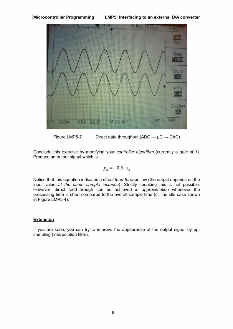
a quick test should always be done before you apply a signal to the microcontroller! Run your program and measure both input signal (from the function generator) and output signal (from the DAC). You should end up with a display similar to that shown in Figure LMP5-7 (CH1: DAC output, CH2: ADC input). Now change the frequency of your input signal. At what frequency does the output signal no longer resemble a sine wave? At what frequency would you expect aliasing to occur? How many conversions per period are required to represent a signal without loss of information? Set the frequency to 100 Hz. Zoom into the trace of the output signal and observe its step like characteristic. How does this relate to the resolution of the DAC? What would be the appropriate thing to do to make this signal look a little ‘nicer’?
Microcontroller Programming LMP5: Interfacing to an external D/A converter
8
Figure LMP5-7 Direct data throughput (ADC → µC → DAC) Conclude this exercise by modifying your controller algorithm (currently a gain of 1). Produce an output signal which is
nn xy ⋅−= 5.0
Notice that this equation indicates a direct feed-through law (the output depends on the input value at the same sample instance). Strictly speaking this is not possible. However, direct feed-through can be achieved in approximation whenever the processing time is short compared to the overall sample time (cf. the idle case shown in Figure LMP5-4).
Extension If you are keen, you can try to improve the appearance of the output signal by up-sampling (interpolation filter).