arm microcontroller interfacing tutorial -...
TRANSCRIPT

MicrocontrollerInterfacingCSE/EE5/7385MicrocontrollerArchitectureandInterfacing
DavidHoungninou
SouthernMethodistUniversity
Tableofcontent
1. Targetdevice:MCBSTM32C
2. References
3. GPIOports:registersandpins
4. InterfacingwiththeLEDs
2
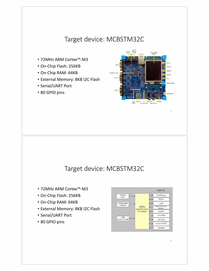
Targetdevice:MCBSTM32C
• 72MHzARMCortex™-M3
• On-ChipFlash:256KB• On-ChipRAM:64KB
• ExternalMemory:8KBI2CFlash
• Serial/UARTPort• 80GPIOpins
3
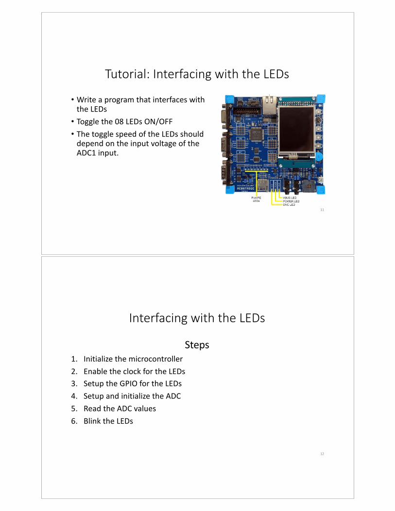
Targetdevice:MCBSTM32C
• 72MHzARMCortex™-M3
• On-ChipFlash:256KB• On-ChipRAM:64KB
• ExternalMemory:8KBI2CFlash
• Serial/UARTPort• 80GPIOpins
4

Usefulreferences
• Evaluationboard:MCBSTM32C
• Microcontroller:STM32F107VC
• Manufacturer:STMicroelectronics
• Boarddocumentation:www.keil.com/dd/chip/4889.htm
• Boardschematic:
www.keil.com/mcbstm32c/mcbstm32c-base-board-schematics.pdf
• MicrocontrollerReferencemanual:RM0008davidkebo.com/documents/RM0008_Reference_manual.pdf
5
WhatisaGPIOport?
• AGPIOportisagroupofuser-configurablepinsforGeneralPurposeInput/Output• TheSTM32F107VChas7generalpurposeinput/output(GPIO)ports
• The7GPIOPortsareA,B,C,D,E,FandG.• Eachportcanhaveupto16pins• Eachporthas7registers
6

WhatisaGPIOport?
7
WhatisaGPIOpin?
A GPIO pin is a generic pincontrollable by the user atrun time and configurableto be input or output.
Input
Output
8

WhatisaGPIOregister?
AGPIO registerisa32-bit storagearea thatholdconfigurationbitsforaGPIOpin
Exampleofaconfigurable32-bit register
9
7GPIOportregisters(32-bit)
• ConfigurationregisterlowGPIOx_CRL• ConfigurationregisterhighGPIOx_CRH• InputdataregisterGPIOx_IDR• OutputdataregisterGPIOx_ODR• Set/resetregisterGPIOx_BSRR• ResetregisterGPIOx_BRR• LockingregisterGPIOx_LCKR
the'x' istheportname.e.g.GPIOA_IDRistheinputdataregisterassociatedwithportA.
(Reference:RM0008Page170)
10
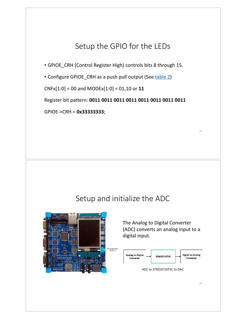
Tutorial:InterfacingwiththeLEDs
• WriteaprogramthatinterfaceswiththeLEDs
• Togglethe08LEDsON/OFF• ThetogglespeedoftheLEDsshoulddependontheinputvoltageoftheADC1input.
11
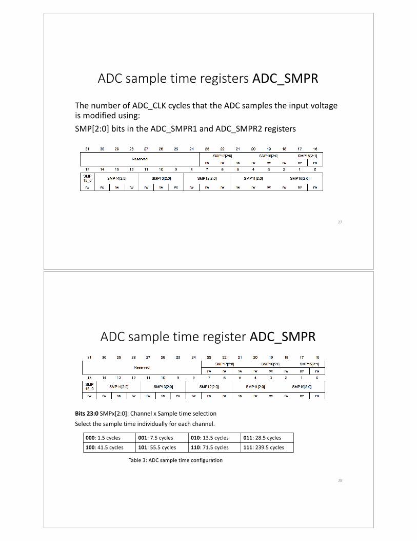
InterfacingwiththeLEDs
Steps1. Initializethemicrocontroller
2. EnabletheclockfortheLEDs
3. SetuptheGPIOfortheLEDs
4. SetupandinitializetheADC
5. ReadtheADCvalues
6. BlinktheLEDs
12

Initializethemicrocontroller
SystemInit()isafunctiondefinedinthesourcefilesystem_stm32f10x_cl.c
Thepurposeofthisfunctionisto:
• Initializetheembeddedflashinterface
• Updatethesystemclockfrequency
13
EnabletheclockfortheLEDs
• TheARMmicrocontrollerdoesnotholdtheclockactivecontinuously
• EnabletheclockfortheLEDsmanually(PortE)• Setconfigurationbit(s)inregisterRCC_APB2ENR• RCC_APB2ENR:AdvancedPeripheralBus2EnableRegister
RCC->APB2ENR|=1<<6; //EnableGPIOEclock14

SetuptheGPIOfortheLEDs
• LEDspinsarewiredtoGPIOE(PortE)• The16pinsarePE0toPE15• LEDsarewiredtopinsPE8,…PE15• Configurethepinsasoutput
GPIOE->CRH=0x33333333;
15
SetuptheGPIOfortheLEDsName r/w Bits Function
GPIOx_CRL Portconfigurationregisterlow rw CNF[1:0],MODE[1:0] Configurelowest8bitofport x.INorOUT
GPIOx_CRH Portconfigurationregisterhigh rw CNF[1:0],MODE[1:0] Configurehighest8bitofport x.INorOUT
GPIOx_IDR portinputdataregister r IDR[15:0]Readstateofpinsconfiguredforinputonport x (Lowest16bitsofword)
GPIOx_ODR portoutputdataregister rw ODR[15:0]WritetopinsconfiguredforOutputonport x (Lowest16bitsofword)
GPIOx_BSRR Portbitset/resetregister w BS[15:0],BR[15:0]AtomicSet/ResetindividualPinsconfiguredforOutput.
GPIOx_BRR Portbitresetregister w BR[15:0]AtomicResetindividualPinsconfiguredforOutput.(Lowest16bitsofword)
GPIOx_LCKR Portconfigurationlockregister rw LCK[15:0],LCKKLockindividualpinsofport x (FreezeCRLandCRHofports)
Table1:GPIOConfigurationRegisters16

SetuptheGPIOfortheLEDsConfigurationmode CNF1 CNF0 MODE1 MODE0 PxODRregister
GeneralPurposeOutput
Push-Pull0
0
011011
0or1
OpenDrain 1 0or1
AlternatefunctionOutput
Push-Pull1
0 Don'tCare
OpenDrain 1 Don'tCare
Input
Analog0
0
00
Don'tCare
Floating 1 Don'tCare
Pull-Down1 0
0
Pull-Up 1
Portconfigurationregistertopins Table2:Portbitconfigurationsummary 17
SetuptheGPIOfortheLEDs
Portconfigurationregisterlow(GPIOx_CRL)(x=A..G)
Portconfigurationregisterhigh(GPIOx_CRH)(x=A..G)
18
SetuptheGPIOfortheLEDs
• GPIOE_CRH(ControlRegisterHigh)controlsbits8through15.
• ConfigureGPIOE_CRHasa pushpulloutput (Seetable2)
CNFx[1:0]=00andMODEx[1:0]=01,10or11
Registerbitpattern:0011 0011 0011 0011 0011 0011 0011 0011
GPIOE->CRH=0x33333333;
19
SetupandinitializetheADC
TheAnalogtoDigitalConverter(ADC)convertsananaloginputtoadigitalinput.
ADCtoSTM32F107VCtoDAC
20

SetupandinitializetheADC
EnabletheclockfortheADC.
RCC->APB2ENR|=1 <<9;
APB2peripheralclockenableregister(RCC_APB2ENR)
21
SetupandinitializetheADC
• ThepotentiometerconnectstoportpinPC4(ADC12_IN14)
• PinPC4mustbeconfiguredasananaloginput.(Seetable2)
• Pin4isconnectedtoCRL(Configurationregisterlow)ToconfigurePC4weusethefollowingmask:
1111 1111 1111 0000 1111 1111 1111 1111
AbitwiseANDofGPIOC->CRLandthemaskclearsCNF4andMODE4
GPIOC->CRL&=0xFFF0FFFF;
22

SetuptheADC
Portconfigurationregisterlow(GPIOx_CRL)(x=A..G)
Portconfigurationregisterhigh(GPIOx_CRH)(x=A..G)
23
ADCSequenceregisters
TheSTM32F107has18analoginputchannels.
Sequenceregistersconfigurethenumberofchannelstosample
24

ADCSequenceregisters
Bits23:20L[3:0]:Regularchannelsequencelength.Numberofconversionsintheregularchannelconversionsequence.
0000:1conversion,0001:2conversions,...1111:16conversionsBits19:15SQ16[4:0]:16thconversioninregularsequence.Channelnumberassignedasthe16thintheconversionsequence.
Bits14:10SQ15[4:0]:15thconversioninregularsequence
25
ADCSequenceregisters
TheSTM32F107has18analoginputchannels.Thepotentiometeriswiredtochannel14Forasingleconversion:ADC1->SQR1=0x00000000;//RegularchannelsingleconversionADC1->SQR2=0x00000000;//Clear register
ADC1->SQR3=(14<<0); //channel14as1stconversion
26
ADCsampletimeregistersADC_SMPR
ThenumberofADC_CLKcyclesthattheADCsamplestheinputvoltageismodifiedusing:
SMP[2:0]bitsintheADC_SMPR1andADC_SMPR2registers
27
ADCsampletimeregisterADC_SMPR
Bits23:0SMPx[2:0]:ChannelxSampletimeselection
Selectthesampletimeindividuallyforeachchannel.
28
000:1.5cycles 001:7.5cycles 010:13.5cycles 011:28.5cycles
100:41.5cycles 101:55.5cycles 110:71.5cycles 111:239.5cycles
Table3:ADCsampletimeconfiguration

ADCsampletimeregisterADC_SMPR
29
TheADCshoulddelayreadingfor5.15uS
ForanADCCLKrunningat14MHz
Determinethesampletime(SettingforSMPx)?
ADCsampletimeregisterADC_SMPR
30
TheADCshoulddelayreadingfor5.15uS
ForanADCCLKrunningat14MHz
Determinethesampletime(SettingforSMPx)?
T=1/14MHz
T=0.07142uS
#of cycles =5.15uS /T=5.15uS /0.07142uS
#of cycles =72
ADCSampleTimeBitsRegister
Setchannel14atasampletimeof72cycles:
Thebitconfigurationfor72cyclesis110(Table3)
ADC1->SMPR1=6<<12;
ADC1->SMPR2=0x00000000;//Clearregister
31
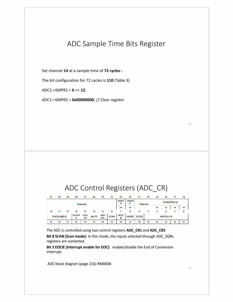
ADCControlRegisters(ADC_CR)
32
TheADCiscontrolledusingtwocontrolregistersADC_CR1 andADC_CR2Bit8SCAN(Scanmode):Inthismode,theinputsselectedthroughADC_SQRxregistersareconverted.
Bit5EOCIE (InterruptenableforEOC): enable/disabletheEndofConversioninterrupt.
ADCblockdiagram(page216)RM0008
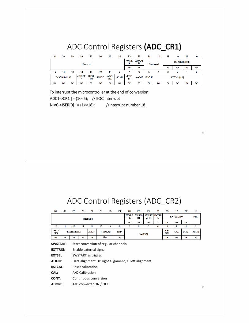
ADCControlRegisters(ADC_CR1)
33
Tointerruptthemicrocontrollerattheendofconversion:
ADC1->CR1|=(1<<5); //EOCinterrupt
NIVC->ISER[0]|=(1<<18); //Interruptnumber18
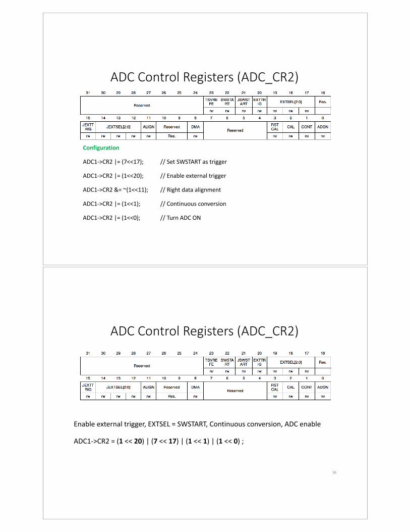
ADCControlRegisters(ADC_CR2)
34
SWSTART: Startconversionofregularchannels
EXTTRIG: Enableexternalsignal
EXTSEL SWSTARTastrigger.
ALIGN: Dataalignment.0:rightalignment, 1:leftalignment
RSTCAL: Resetcalibration
CAL: A/DCalibration
CONT: Continuousconversion
ADON: A/DconverterON/OFF
ADCControlRegisters(ADC_CR2)
35
Configuration
ADC1->CR2|=(7<<17); //SetSWSTARTastrigger
ADC1->CR2|=(1<<20); //Enableexternaltrigger
ADC1->CR2&=~(1<<11); // Rightdata alignment
ADC1->CR2|=(1<<1); // Continuousconversion
ADC1->CR2|=(1<<0); //TurnADCON
ADCControlRegisters(ADC_CR2)
Enableexternaltrigger,EXTSEL=SWSTART,Continuousconversion,ADCenable
ADC1->CR2=(1 <<20)|(7<<17)| (1 <<1) |(1<<0);
36
ADCControlRegisters(ADC_CR2)
37
CalibrationADC1->CR2|=(1<<3); //resetcalibration
while(ADC1->CR2&(1<<3)); //waituntilresetfinished
ADC1->CR2|=(1<<2); //startcalibration
while(ADC1->CR2&(1<<2)); //waituntilcalibrationfinished
ConversionADC1->CR2|=(1<<22); //start SWconversion
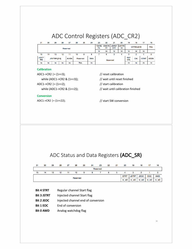
ADCStatusandDataRegisters(ADC_SR)
38
Bit4STRT RegularchannelStartflag
Bit3JSTRT InjectedchannelStartflag
Bit2JEOC Injectedchannelendofconversion
Bit1EOC Endofconversion
Bit0AWD Analogwatchdogflag
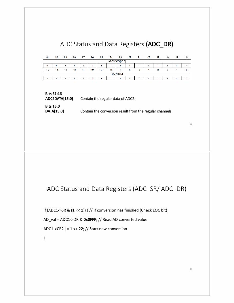
ADCStatusandDataRegisters(ADC_DR)
39
Bits31:16ADC2DATA[15:0] ContaintheregulardataofADC2.
Bits15:0DATA[15:0] Containtheconversionresultfromtheregularchannels.
ADCStatusandDataRegisters(ADC_SR/ADC_DR)
if (ADC1->SR&(1 <<1)){//Ifconversionhasfinished(CheckEOCbit)
AD_val =ADC1->DR&0x0FFF;//ReadADconvertedvalue
ADC1->CR2|=1 <<22;//Startnewconversion
}
40
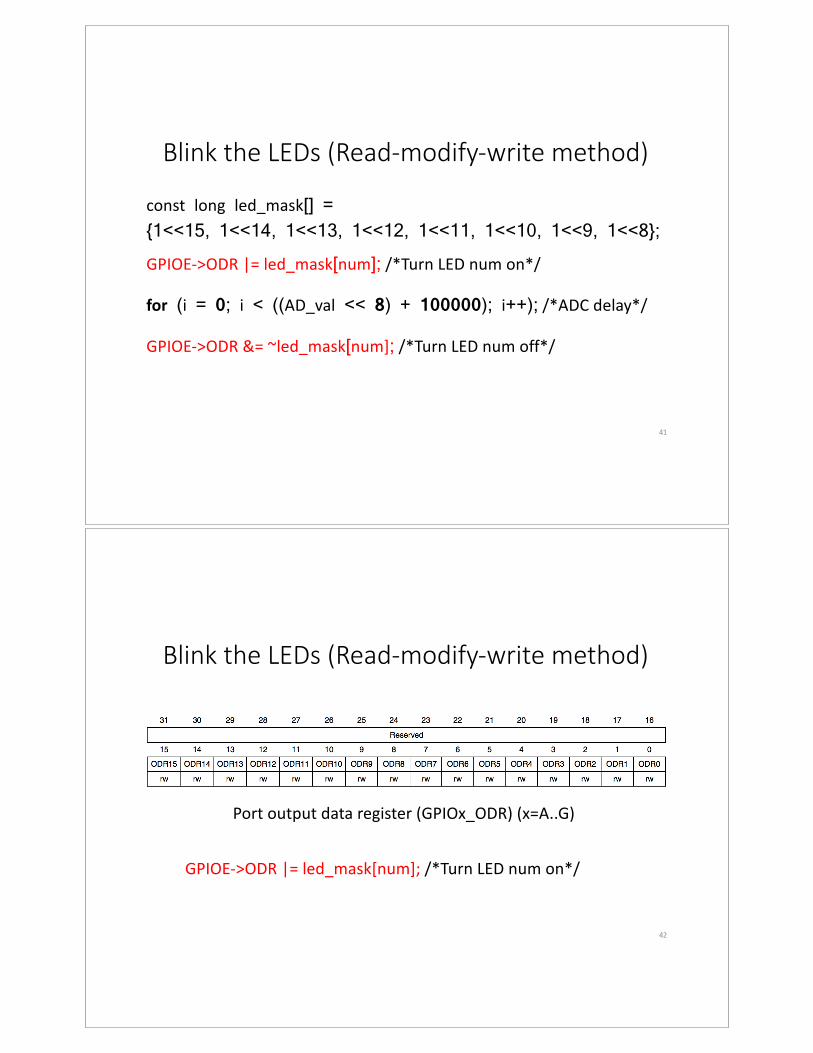
BlinktheLEDs(Read-modify-writemethod)
const long led_mask[] = {1<<15, 1<<14, 1<<13, 1<<12, 1<<11, 1<<10, 1<<9, 1<<8};GPIOE->ODR|=led_mask[num]; /*Turn LEDnum on*/
for (i = 0; i < ((AD_val << 8) + 100000); i++); /*ADCdelay*/
GPIOE->ODR&=~led_mask[num]; /*Turn LEDnum off*/
41
BlinktheLEDs(Read-modify-writemethod)
42
GPIOE->ODR|=led_mask[num]; /*Turn LEDnum on*/
Portoutputdataregister(GPIOx_ODR)(x=A..G)
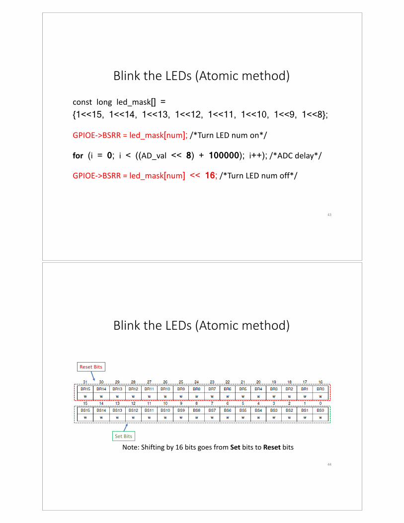
BlinktheLEDs(Atomicmethod)
const long led_mask[] = {1<<15, 1<<14, 1<<13, 1<<12, 1<<11, 1<<10, 1<<9, 1<<8};
GPIOE->BSRR=led_mask[num]; /*Turn LEDnum on*/
for (i = 0; i < ((AD_val << 8) + 100000); i++); /*ADCdelay*/GPIOE->BSRR=led_mask[num] << 16; /*Turn LEDnum off*/
43
BlinktheLEDs(Atomicmethod)
SetBits
ResetBits
Note:Shiftingby16bitsgoesfromSet bitstoReset bits
44

Timers
Timersareclocksourcesusedasthe‘heartbeats’foroperations.
e.g.ofapplicationsusingtimers:• Countingpulses• Measuringtimeperiodsofwaveforms
• Generatingpulsewidthmodulation(PWM)signals
• Triggeringexternaldevices• Timingspecialevents
45
Timers
03groupsoftimers:
• BasicTimers
• GeneralPurposeTimers
• AdvancedTimers (TIM1&TIM8)
46

Basictimers
TIM6,TIM7
Applications:noI/Ochannelsforinputcapture
noPWMgeneration
Onlyusedfortime-basegeneration
47
GeneralPurposeTimers
TIM2,TIM3,TIM4,TIM5
Applications:• PWMgeneration
• Inputcapture• Time-basegeneration
• Outputcompare
48

Advancedtimers
TIM1,TIM8
Applications:• AdvancedPWMgeneration
• Inputcapture• Time-basegeneration
• Outputcompare
49
Timerspin
EachtimerisassociatedwithanI/Opin
Configurethealternatefunctiontousethetimerpin
Whatisanalternatefunction?InadditiontogeneralpurposeinputandoutputtheARMsubsystemcanimplementotherspecializedinputoutputfunctions.
e.g.TIM4_Ch4 isanalternatefunctionforpinPB9
50

TIMx functionaldescription
Themainblockofthetimerisa16-bitcounterTIMx_CNT withanauto-reloadregister TIMx_ARRThecountercancountup,downorbothupanddown.
Thecounterclockcanbedividedbyapre-scalerTIMx_PSC
51General-purposetimers(TIM2toTIM5)RM0008Manual15.1Page364
TIMx functionaldescription
Countertimingdiagramwithpre-scalerdivisionchangefrom1to2
52
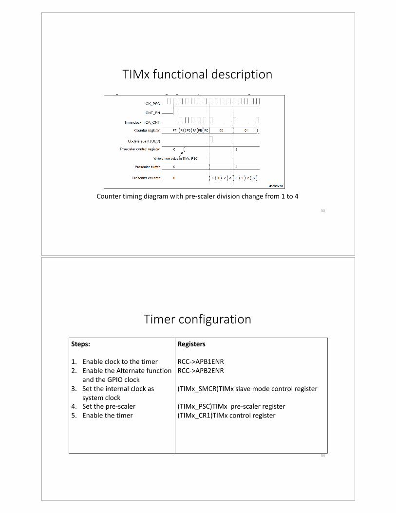
TIMx functionaldescription
Countertimingdiagramwithpre-scalerdivisionchangefrom1to4
53
Timerconfiguration
54
Steps:
1. Enableclocktothetimer2. EnabletheAlternatefunction
andtheGPIOclock3. Settheinternal clockas
systemclock4. Setthepre-scaler5. Enablethetimer
Registers
RCC->APB1ENRRCC->APB2ENR
(TIMx_SMCR)TIMx slavemodecontrolregister
(TIMx_PSC)TIMx pre-scalerregister(TIMx_CR1)TIMx controlregister
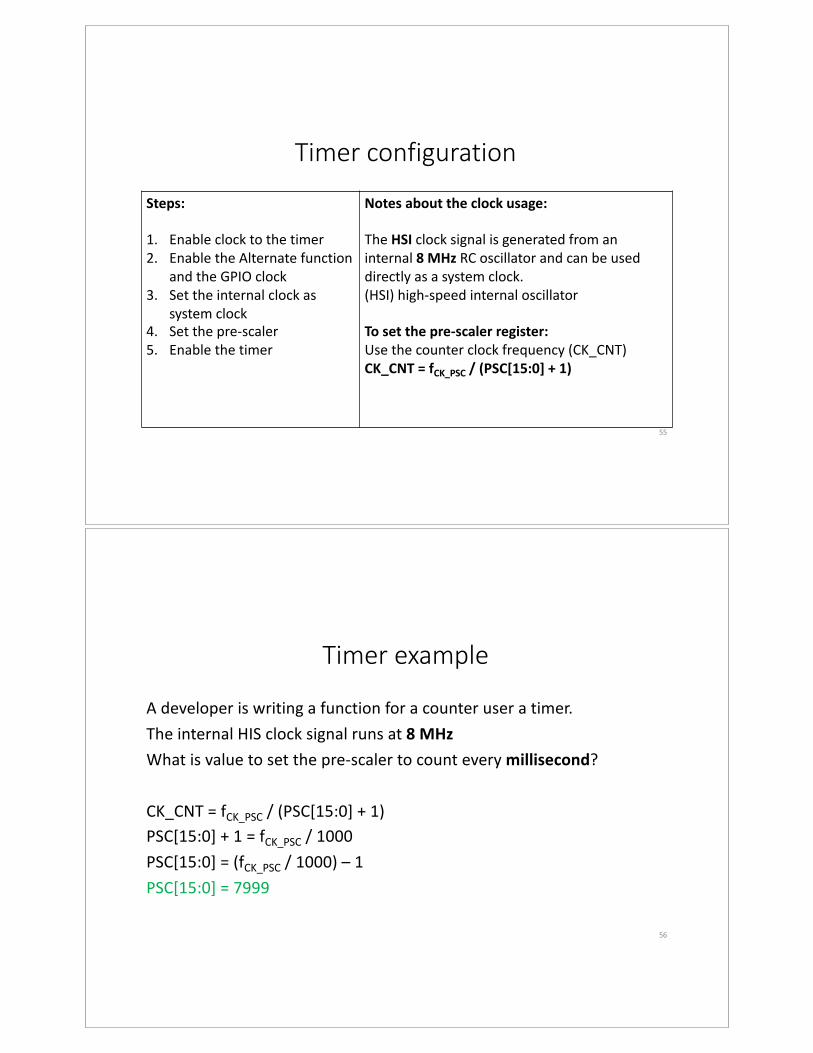
Timerconfiguration
55
Steps:
1. Enableclocktothetimer2. EnabletheAlternatefunction
andtheGPIOclock3. Settheinternal clockas
systemclock4. Setthepre-scaler5. Enablethetimer
Notes abouttheclockusage:
TheHSI clocksignalisgeneratedfromaninternal8MHzRCoscillatorandcanbeuseddirectlyasasystemclock.(HSI)high-speedinternaloscillator
Tosetthepre-scalerregister:Usethecounterclockfrequency(CK_CNT)CK_CNT=fCK_PSC /(PSC[15:0]+1)
Timerexample
Adeveloperiswritingafunctionforacounteruseratimer.
TheinternalHISclocksignalrunsat8MHzWhatisvaluetosetthepre-scalertocounteverymillisecond?
CK_CNT=fCK_PSC /(PSC[15:0]+1)
PSC[15:0]+1=fCK_PSC /1000
PSC[15:0]=(fCK_PSC /1000)– 1
PSC[15:0]=7999
56
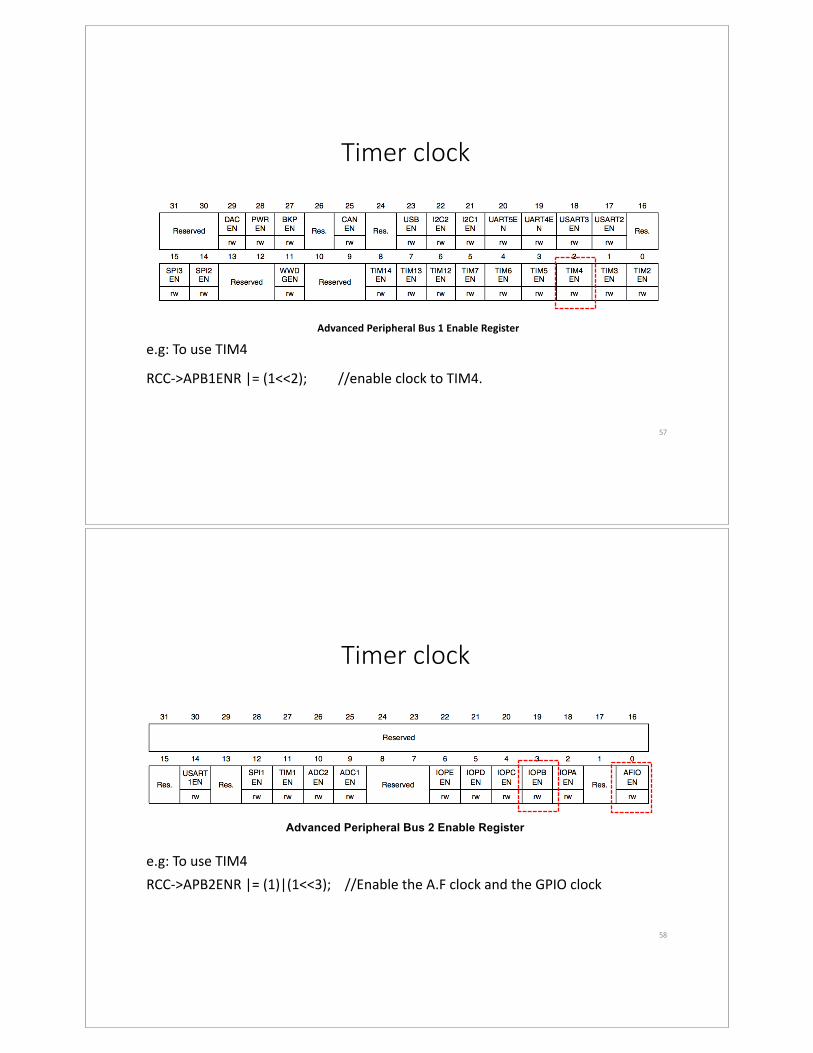
Timerclock
57
e.g:TouseTIM4
RCC->APB1ENR|=(1<<2); //enableclocktoTIM4.
AdvancedPeripheralBus1EnableRegister
Timerclock
58
e.g:TouseTIM4
RCC->APB2ENR|=(1)|(1<<3); //EnabletheA.FclockandtheGPIOclock
Advanced Peripheral Bus 2 Enable Register

Timerpre-scalerregister
59
TIM1&TIM8pre-scaler(TIMx_PSC)PSC[15:0]:Pre-scalervalue
Timerslavemoderegister
60
TIM1&TIM8slavemodecontrolregister(TIMx_SMCR)SMS=000,thepre-scalerisclockeddirectlybytheinternalclock.

Timercontrolregister
61
TIM1&TIM8controlregister1(TIMx_CR1)CEN:Counterenable0:Counterdisabled1:Counterenabled