mercuryplus technical reference
TRANSCRIPT

Technical ReferenceMERCURYplus NMR Spectrometer Systems
Pub. No. 01-999187-00, Rev. B1002

Technical ReferenceMERCURYplus NMR Spectrometer Systems
Pub. No. 01-999187-00, Rev. B1002

MERCURYplus Technical ReferenceMERCURYplus NMR Spectrometer SystemsPub. No. 01-999187-00, Rev. B1002
Applicability of manual:MERCURYplus NMR spectrometer systems
Technical contributors: Frits Vosman, Emil Johnson, Herman EggerTechnical writer: Mike MillerTechnical editor: Dan Steele
Revision history:A0401 – Initial release, ER ####B1002 – Update to latest Mercury specifications.
Copyright 2001, 2002 by Varian, Inc.3120 Hansen Way, Palo Alto, California 943041-800-356-4437http://www.varianinc.comAll rights reserved. Printed in the United States.
The information in this document has been carefully checked and is believed to be entirely reliable. However, no responsibility is assumed for inaccuracies. Statements in this document are not intended to create any warranty, expressed or implied. Specifications and performance characteristics of the software described in this manual may be changed at any time without notice. Varian reserves the right to make changes in any products herein to improve reliability, function, or design. Varian does not assume any liability arising out of the application or use of any product or circuit described herein; neither does it convey any license under its patent rights nor the rights of others. Inclusion in this document does not imply that any particular feature is standard on the instrument.
MERCURYplus, UNITYINOVA, VNMR, VnmrS, VnmrX, VnmrI, VnmrV, VnmrSGI, MAGICAL II, AutoLock, AutoShim, AutoPhase, limNET, ASM, and SMS are registered trademarks or trademarks of Varian, Inc. Sun, Solaris, CDE, Suninstall, Ultra, SPARC, SPARCstation, SunCD, and NFS are registered trademarks or trademarks of Sun Microsystems, Inc. and SPARC International. Oxford is a registered trademark of Oxford Instruments LTD.Ethernet is a registered trademark of Xerox Corporation. VxWORKS and VxWORKS POWERED are registered trademarks of WindRiver Inc. Other product names in this document are registered trademarks or trademarks of their respective holders.

01-999187-00 B1002 MERCURYplus Technical Reference 3
Table of Contents
Introduction ............................................................................................. 9
Chapter 1. Host Computer .................................................................... 111.1 User Interface .............................................................................................................. 11
1.2 Hardware ..................................................................................................................... 12
Chapter 2. NMR Console – Digital Section ......................................... 132.1 Acquisition CPU ......................................................................................................... 13
2.2 STM/Output Board ..................................................................................................... 14Block Diagram (Sheet 1) .................................................................................... 14Line Drivers (Sheet 2) ........................................................................................ 14Address Decoder (Sheet 3) ................................................................................. 14Programmable DRAM (Sheet 4) ........................................................................ 15STM Section (Sheet 5) ....................................................................................... 15Line Drivers (Sheet 6) ........................................................................................ 16Pre-FIFOs (Sheet 7) ............................................................................................ 16Loop-FIFOs (Sheet 8) ......................................................................................... 16Output Controller (Sheet 9) ................................................................................ 16Bypass Capacitors (Sheet 10) ............................................................................. 16Specifications ..................................................................................................... 17
2.3 16-Bit Analog-to-Digital Conversion (ADC) Board .................................................. 23Power Requirements ........................................................................................... 23VME Bus Interface (Sheet 2) ............................................................................. 23Input Selector/Differential Amplifiers (Sheet 3) ................................................ 23Lock ADC Channel (Sheet 4) ............................................................................. 24Signal Buffers (Sheet 5) ..................................................................................... 25PAL _kraddec Inputs and Outputs ...................................................................... 25PAL _fctdec Inputs and Outputs ......................................................................... 26PAL _ovld_de Inputs and Outputs ...................................................................... 27PAL _admod Inputs and Outputs ........................................................................ 28
Chapter 3. NMR Console – RF Section ............................................... 293.1 Junction Board ............................................................................................................ 30
Specifications ..................................................................................................... 30Safety Interlock .................................................................................................. 33Typical Power Consumption .............................................................................. 33AP Bus Buffer (Sheet 1) ..................................................................................... 3340-MHz Reference (Sheet 2) .............................................................................. 33Decoupler Band Select (Sheet 3) ........................................................................ 34Decoupler Modulation Circuit (Sheet 4) ............................................................ 35Comparator (Sheet 5) ......................................................................................... 35DC Power Inputs (Sheet 6) ................................................................................. 36PAL _lkgate Inputs and Outputs ......................................................................... 36PAL _lkoutputs Inputs and Outputs .................................................................... 37
Table of Contents
4 MERCURYplus Technical Reference 01-999187-00 B1002
PAL _ogates Inputs and Outputs ........................................................................ 38PAL addrmux Inputs and Outputs ...................................................................... 39
3.2 High/Low-Band Reference Generator ........................................................................ 39Block Diagram (Sheet 8) .................................................................................... 40Input .................................................................................................................... 41Output ................................................................................................................. 41
3.3 5-Nuclei Reference Generator – 200 MHz ................................................................. 42Block Diagram (Sheet 6) .................................................................................... 42Input .................................................................................................................... 43Output ................................................................................................................. 43
3.4 Low-Band Transmitter ................................................................................................ 43Block Diagram (Sheet 6) .................................................................................... 44Input .................................................................................................................... 45Output ................................................................................................................. 45
3.5 Broadband Observe Receiver ..................................................................................... 46Block Diagram (Sheet 7) .................................................................................... 46Input .................................................................................................................... 47Output ................................................................................................................. 47
3.6 High-Band Transmitter, Hetero Decoupler ................................................................. 48Block Diagram (Sheet 6) .................................................................................... 49Input .................................................................................................................... 49Output ................................................................................................................. 50
3.7 Homonuclear Decoupler ............................................................................................. 50Block Diagram (Sheet 6) .................................................................................... 50Input .................................................................................................................... 51Output ................................................................................................................. 51
3.8 Lock Transmitter – 200 MHz ...................................................................................... 52Block Diagram (Sheet 8) .................................................................................... 52Input .................................................................................................................... 53Output ................................................................................................................. 53
3.9 Lock Transmitter – 300, 400 MHz .............................................................................. 53Block Diagram (Sheet 8) .................................................................................... 54Input .................................................................................................................... 55Output ................................................................................................................. 55
3.10 Broadband Lock Receiver ........................................................................................ 56Block Diagram (Sheet 7) .................................................................................... 56Input .................................................................................................................... 57Output ................................................................................................................. 57General Specifications ........................................................................................ 57
3.11 Shim DAC/Driver ..................................................................................................... 58Power Requirements ........................................................................................... 58Specifications ..................................................................................................... 58Buffer U6B (Sheet 1) .......................................................................................... 59DAC Package (Sheet 2) ...................................................................................... 59Reset Circuit (Sheet 3) ........................................................................................ 61Buffer Circuits (Sheet 4) .................................................................................... 61DAC Outputs (Sheet 5) ...................................................................................... 62Axial Resistor Matrixes (Sheets 6 and 7) ........................................................... 62Radial Shim Drive Circuits (Sheets 8 and 9) ...................................................... 62

Table of Contents
01-999187-00 B1002 MERCURYplus Technical Reference 5
Power Circuits (Sheet 10) ................................................................................... 62Spare Packages (Sheet 11) .................................................................................. 63Block Diagram (Sheet 12) .................................................................................. 63
Chapter 4. Magnet Interface Box (MIB) ............................................... 654.1 Low-Band Broadband Preamp – 200-, 300-, 400-MHz Systems ............................... 66
4.2 Lock Preamplifier – 200-, 300-, 400-MHz Systems ................................................... 66
4.3 High-Band Preamplifier – 200-, 300-, 400-MHz Systems ......................................... 67
4.4 Auto Liq/Sol Spinner Board ....................................................................................... 68Block Diagram (Sheet 1) .................................................................................... 69Micro Controller (Sheet 2) ................................................................................. 69Probe Tune Signal/Spinner Signals (Sheet 3) ..................................................... 69DAC (Sheet 4) .................................................................................................... 70
4.5 Probe, Q-Tune Detector .............................................................................................. 71Block Diagram (Sheet 1) .................................................................................... 71Input .................................................................................................................... 71Output ................................................................................................................. 72
4.6 Automated Deuterium Gradient Shimming Relay ...................................................... 72
Chapter 5. Power Supply ...................................................................... 735.1 System Power Supply ................................................................................................. 73
5.2 High-Band, High-Power RF Amplifier – 200-, 300-, 400-MHz Systems .................. 75
5.3 Low-Band, High-Power RF Amplifier – 200-, 300-, 400-MHz Systems ................... 76
5.4 High-Band, Low-Power RF Amplifier – 200-, 300-MHz Systems ............................ 77
5.5 Low-Band, Low-Power RF Amplifier – 200-, 300-MHz Systems ............................. 78
5.6 Dual Channel RF Amplifier – 300-, 400-MHz Systems ............................................ 79
Chapter 6. Options ................................................................................ 816.1 Pulsed Field Gradient (PFG) Amplifier ...................................................................... 82
Performa I PFG ................................................................................................... 82Performa II PFG ................................................................................................. 85
6.2 PFG Interface Board ................................................................................................... 87Block Diagram (Sheet 1) .................................................................................... 87Wavegen Circuit (Sheet 2) .................................................................................. 88AP Bus (Sheet 3) ................................................................................................ 88Output (Sheet 4) ................................................................................................. 89Diagnostics (Sheet 4) .......................................................................................... 89Initialization (Sheet 4) ........................................................................................ 89Addresses ............................................................................................................ 89AP DAC Loading Sequence .............................................................................. 90Other I/O Signals ............................................................................................... 90
6.3 CP/MAS Accessory .................................................................................................... 90
6.4 Variable Temperature (VT) Unit ................................................................................. 91Status Indicators ................................................................................................. 92Protection ............................................................................................................ 92
6.5 Automated Sample Management ................................................................................ 93
Index ....................................................................................................... 95

6 MERCURYplus Technical Reference 01-999187-00 B1002
List of Figures
Figure 1. Host Computer System ................................................................................................... 11
Figure 2. Digital Card Cage (NMR Console)................................................................................. 13
Figure 3. RF Section (NMR Console) ............................................................................................ 29
Figure 4. Magnet Interface Box (MIB)........................................................................................... 65
Figure 5. Preamplifier Block Diagram ........................................................................................... 68
Figure 6. System Power Supply ..................................................................................................... 73
Figure 7. Console Options .............................................................................................................. 81

01-999187-00 B1002 MERCURYplus Technical Reference 7
List of Tables
Table 1. STM/Output Board LED Descriptions ............................................................................ 15
Table 2. STM/Output Board VME Address Space ........................................................................ 17
Table 3. VME Software Reset and Output Controls Register ....................................................... 17
Table 4. VME Interrupt Register ................................................................................................... 18
Table 5. STM Interrupt Status Register ......................................................................................... 18
Table 6. VME Interrupt Mask Register ......................................................................................... 18
Table 7. VME High-Speed Lines Register .................................................................................... 19
Table 8. VME Output Interrupt Status and Miscellaneous Register ............................................. 19
Table 9. VME AP Bus Register ..................................................................................................... 20
Table 10. VME Interrupt Vector Table .......................................................................................... 20
Table 11. FIFO Word Definition .................................................................................................... 20
Table 12. Time Base Definition ..................................................................................................... 21
Table 13. Special Definition of FF[26:24] ..................................................................................... 21
Table 14. STM AP Bus Registers .................................................................................................. 21
Table 15. STM Control Register .................................................................................................... 22
Table 16. STM Interrupt Mask ...................................................................................................... 22
Table 17. Phase Cycling Modes ..................................................................................................... 22
Table 18. Status Decoder and Sync Selector PAL ......................................................................... 23
Table 19. Status Register Definition .............................................................................................. 24
Table 20. Control Register Definition ........................................................................................... 24
Table 21. 16-Bit ADC Board PAL _kraddec Input and Output ..................................................... 25
Table 22. 16-Bit ADC Board PAL _fctdec Inputs and Outputs ..................................................... 26
Table 23. 16-Bit ADC Board PAL _ovld_de Inputs and Outputs ................................................. 27
Table 24. 16-Bit ADC Board PAL _admod PAL ........................................................................... 28
Table 25. Junction Board LEDs ..................................................................................................... 30
Table 26. Junction Board Inputs .................................................................................................... 31
Table 27. Junction Board Output ................................................................................................... 32
Table 28. Junction Board Output Signals ...................................................................................... 34
Table 29. Junction Board DMF ..................................................................................................... 35
Table 30. Safety Status Bits ........................................................................................................... 35
Table 31. Junction Board PAL _lkgate Inputs and Outputs ........................................................... 36
Table 32. Junction Board PAL _lkoutputs Inputs and Outputs ...................................................... 37
Table 33. PAL _ogates Inputs and Outputs .................................................................................... 38
Table 34. PAL addrmux Inputs and Outputs .................................................................................. 39
Table 35. Shim/DAC AP Bus Mapping ......................................................................................... 59
Table 36. DAC Loading Format .................................................................................................... 61
Table 37. Low-Band Broadband Preamplifier Connections .......................................................... 66
Table 38. Lock Preamplifier Input Signals .................................................................................... 67
Table 39. Lock Preamplifier Output Signals ................................................................................. 67
Table 40. Auto Liq/Sol Micro Controller Address Map. ............................................................... 69

List of Tables
8 MERCURYplus Technical Reference 01-999187-00 B1002
Table 41. Auto Liq/Sol Control Register Definitions .................................................................... 70
Table 42. Auto Liq/Sol Status Register Definitions ...................................................................... 71
Table 43. Power Supply Input Signals ........................................................................................... 74
Table 44. Power Supply Output Specifications ............................................................................. 74
Table 45. High-Band, High-Power Amplifier Specifications ........................................................ 75
Table 46. Low-Band, High-Power Amplifier Specifications ........................................................ 76
Table 47. High-Band, Low-Power Amplifier Specifications ........................................................ 77
Table 48. Low-Band RF Low-Power Amplifier Specification ...................................................... 78
Table 49. Dual Channel RF Amplifier Specifications ................................................................... 79
Table 50. Basic PFG Specifications ............................................................................................... 83
Table 51. AP Chip Output I/O Register ......................................................................................... 83
Table 52. PFG Constant-Current Output Specifications ................................................................ 83
Table 53. PFG Amplifier Accuracy Specifications ....................................................................... 84
Table 54. Performa II Data Interface ............................................................................................. 86
Table 55. PFG Constant-Current Output Specifications ................................................................ 87
Table 56. VT Specifications .......................................................................................................... 91
Table 57. VT Inputs and Outputs ................................................................................................... 92

01-999187-00 B1002 MERCURYplus Technical Reference 9
Introduction
A basic MERCURYplus NMR spectrometer intended for liquids operation has three major groups of components:
• Host computer system – Includes a Sun workstation with networking capabilities, keyboard, mouse, color monitor, CD-ROM, floppy drive, and a hard-disk drive. Additional hard drives, plotters, printers, and tape units for data storage are available as options.
• NMR console – Includes the rear-mounted rf and digital cardcages, rf amplifiers, and power supplies. The optional pulsed field gradient (PFG) amplifier and variable temperature (VT) control unit are installed in the console. Performa II and CP/MAS are housed in separate enclosures.
• Magnet and Magnet Interface box– Includes the probe, upper barrel, preamplifiers and related electronics, and air supply controls.
This manual provides detailed technical data for all major systems and subsystems. Refer to the manual MERCURYplus System Overview for a brief mechanical and functional description of the spectrometer. The publication System Schematics, MERCURYplus NMR Spectrometer Systemscontains the schematics listed in this manual.
ContentsThis Technical Reference is organized by chapters as follows:
• Chapter 1, ”Host Computer,” briefly introduces the host computer.
• Chapter 2, ”NMR Console – Digital Section,” covers the three printed-circuit boards contained in the digital card cage.
• Chapter 3, ”NMR Console – RF Section,” details the nine printed-circuit boards contained in the rf card cage.
• Chapter 4, ”Magnet Interface Box (MIB),” describes the preamplifiers, Auto Liq/Sol Spinner board, the automated deuterium gradient shimming relay, and the Q-Tune detector.
• Chapter 5, ”Power Supply,” gives an overview of the power supply and rf amplifiers contained in the power supply chassis.
• Chapter 6, ”Options,” describes console optional modules, including the PFG amplifier, PFG Interface board, and VT control unit mounted in the NMR console. It also covers sample changers.
Notational ConventionsA minus sign (–) is used as the last character of a signal name to represent a low true signal. On schematic diagrams, the corresponding notation is a tilde (~).
The syntax (xx:yy) is used to identify a bus containing similar signals, where xx is the most significant bit and yy is the least significant bit.

10 MERCURYplus Technical Reference 01-999187-00 B1002
01-999187-00 B1002 MERCURYplus Technical Reference 11
Chapter 1. Host Computer
Sections in this chapter:
• 1.1 “User Interface” this page
• 1.2 “Hardware” page 12
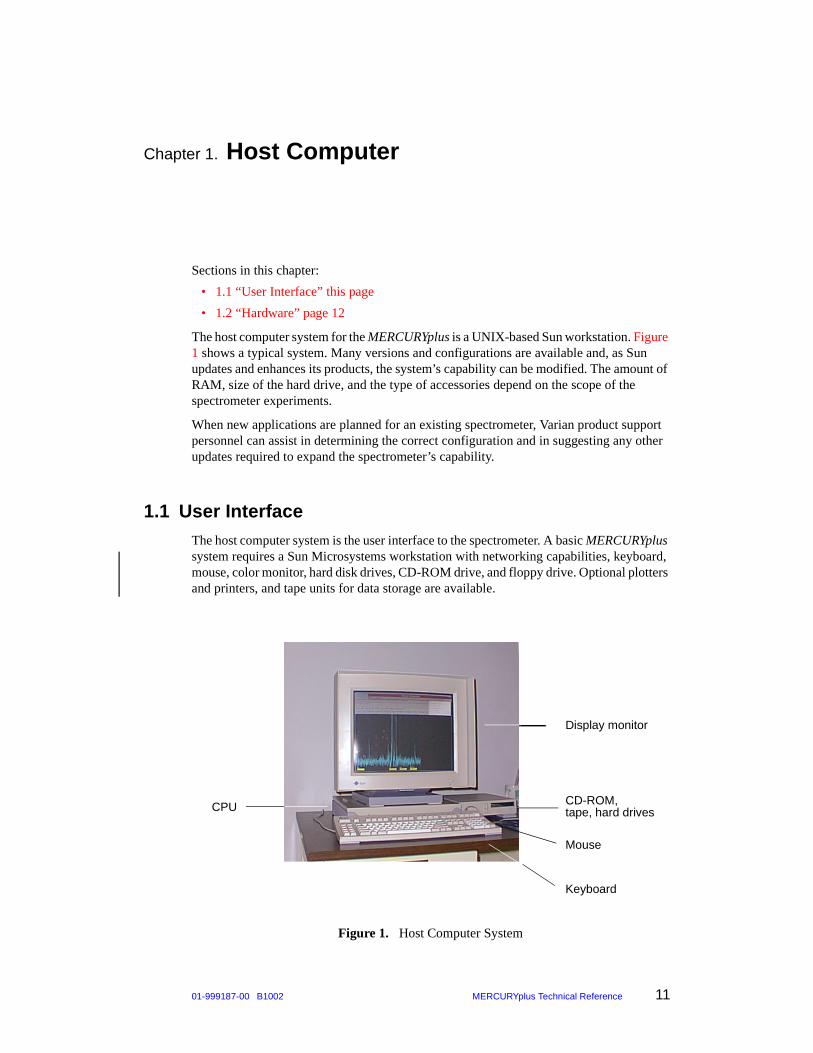
The host computer system for the MERCURYplus is a UNIX-based Sun workstation. Figure 1 shows a typical system. Many versions and configurations are available and, as Sun updates and enhances its products, the system’s capability can be modified. The amount of RAM, size of the hard drive, and the type of accessories depend on the scope of the spectrometer experiments.
When new applications are planned for an existing spectrometer, Varian product support personnel can assist in determining the correct configuration and in suggesting any other updates required to expand the spectrometer’s capability.
1.1 User InterfaceThe host computer system is the user interface to the spectrometer. A basic MERCURYplus system requires a Sun Microsystems workstation with networking capabilities, keyboard, mouse, color monitor, hard disk drives, CD-ROM drive, and floppy drive. Optional plotters and printers, and tape units for data storage are available.
Figure 1. Host Computer System
CPU
Display monitor
CD-ROM,tape, hard drives
Mouse
Keyboard

Chapter 1. Host Computer
12 MERCURYplus Technical Reference 01-999187-00 B1002
The VNMR data acquisition and processing software, and Sun Solaris operating system with CDE (Common Desktop Environment) software installed are resident in the CPU. The CDE software provides the same interface and “look” when Sun, IBM, or SGI data stations are used. In addition, the software can be tailored to the user’s needs and preferences. CDE has a tool bar, file manager, icons, and point-and-click capability.
1.2 HardwareThe display monitor shows FIDs, spectra, system configuration, and other information. The CD-ROM drive is used for loading programs and updating software. Optional larger hard drives, floppy drives, and tape backup drives are also available and are used when large quantities of data are processed.
A larger or second hard drive is recommended if data is to be archivied on the host computer. Otherwise, archival media is required.

01-999187-00 B1002 MERCURYplus Technical Reference 13
Chapter 2. NMR Console – Digital Section
Sections in this chapter:
• 2.1 “Acquisition CPU” this page
• 2.2 “STM/Output Board” page 14
• 2.3 “16-Bit Analog-to-Digital Conversion (ADC) Board” page 23
The MERCURYplus NMR console (see Figure 2) contains the acquisition system electronics, rf section, digital section, and the shim electronics/power supplies. This chapter provides detailed technical descriptions for the three standard circuit boards contained in the digital cardcage.
2.1 Acquisition CPUPart No. 01-905942-00
The Acquisition CPU board is a VME- bus-compatible, single-board microcomputer, based on a Motorola 68040-series microprocessor with 4 serial ports and an Ethernet port. The acquisition CPU uses Wind River System’s VxWorks, a real-time operating system that provides VxWorks-compatible Ethernet protocol for communications with the host.
The CPU is a universal board and includes internal jumpers to establish the correct connections for the spectrometer. Replacement boards are stocked in a standard test configuration with no installed PROMs. When installing a new board, new board jumpers must be placed in exactly the same positions found on the old board. Also, the PROMs from the old board must be installed in the corresponding new board socket and with the same orientation.
Finally, onboard NVRAM should be initialized. For more information, see the manual VNMR and Solaris Software Installation.
Figure 2. Digital Card Cage (NMR Console)
(ADC/STM Cable Cover - Not Shown)

Chapter 2. NMR Console – Digital Section
14 MERCURYplus Technical Reference 01-999187-00 B1002
2.2 STM/Output BoardSchematic No. 01-901367-00, Part No. 01-901364-00
The STM/Output board combines the functions of the traditional sum-to-memory (STM) board and the output board. The board includes:
• The VME bus interface, which uses U4B (01901422 ACTEL ACT1A 1020B FPGA) for interfacing to the VME CPU, VME interrupt handling, decode control signals for the entire board, and DRAM controls; U8B (01901423 ACTEL ACT1A 1010B FPGA) for address and AM code decoding; and a reset and output control register.
• The controller of the output section U5K, which uses the ACTEL ACT3A 1425A programmable FPGA for FIFO, HS line, AP bus, timer, and looping control.
• Six TI 74ACT7808 FIFOs to provide 2048x27 pre-FIFO (3) and 2048x27 loop-FIFO (3).
• A special AP chip U8L, 0090141900, which has two 8-bit output register and uses an ACTEL ACT1A 1010B FPGA.
• The STM section, which uses U4C, 01901421 ACTEL ACT1A 1010B FPGA as the STM acquisition controller, U8E, 01901420 ACTEL ACT2A 1225A FPGA as the address controller, and U4E, 01901436 ACTEL ACT1A 1020B FPGA as the data summing controller.
• Two megabytes of dual-ported DRAM (512K×32 SIMM), which uses a National DP8422A as a DRAM controller.
Block Diagram (Sheet 1)
Sheet 1 gives a block diagram of the STM/Output board.
Line Drivers (Sheet 2)
74ABT16245 line drivers are used to buffer the VME bus data, address, and control lines. This sheet also has the digital +5 V filtering, unused lines, and open collector drivers for VME bus DTACK~, and IRQ4~.
Address Decoder (Sheet 3)
U8B is the address decoder. U8B’s tasks include decoding the VME address and AM code and containing the reset and control register for the output section of this board. U4B is the VME interface. U4B receives the decoded address region from U8B and generates the appropriate enable lines for the entire board. U4B also generates control signals for the DRAM controller, prioritizes interrupts. and contains a VME interrupt mask register and interrupt test register.
U12J is an output status and miscellaneous system status 16-bit VME register. SW1(1-3) is used to set the board revision BD_REV[2:0], and SW1(4) is used to configure the amount of memory on board. When the 512K×32 SIMM is used for a total of 2 MBs, then SW1(4) should be ON, and when 1M×32 SIMM is used for a total of 4 MB, then SW1(4) should be OFF. U12K is a 16-bit latch used to convert 16-bit data from a 16-bit CPU to the 27-bit pre-FIFO data.

2.2 STM/Output Board
01-999187-00 B1002 MERCURYplus Technical Reference 15
Programmable DRAM (Sheet 4)
U8C is the programmable DRAM controller/driver DP8422A that drives the 512K×32 SIMM. U8C is hardwire configured on bootup or at system reset by UR1, UR2, and UR3. For a detailed explanation of the configuration setting of the DRAM controller/driver, refer to the National data book on the DP8422A.
U12D and half of U12C drive the address for U8C when the VME has control of the DRAM indicated by GRANT_VME~ active.
One half of U13G is a LED driver and the other half, in combination with half of U12C, is a HS lines 16-bit VME register. The LEDs display the status (see Table 1) of RUNNING~, FF_MT~, RUN_MT~, INITHALT~, NETBHL~, LOOPING~, APTO~, and HS_CTC~.
STM Section (Sheet 5)
The STM section of this board consists of three FPGAs: U4C, U8E, and U4E.
U4C is the acquisition controller. U4C decodes the AP bus to address the various registers and counters of the STM section, controls the data acquisition and summing process of the NMR data using a state machine, controls the phase cycling of the ADC data, and provides the STM interrupt mask and interrupt status register.
U8E is the address controller. U8E counts down a 24-bit NT counter, counts down a 20-bit NP counter loadable through a 20-bit NP register, increments the source and destination address, provides the 16-bit STM TAG register, drives the address bus of the DRAM controller with the content of the source or destination counter only when the STM section has control of the DRAM, which is signified with GRANT_STM~ active, and provides VME registers to read back the counted values of the NT counter, NP counter, and the content of the TAG register. All the counters and registers are loaded over the AP bus. The source and destination address are 20 bits wide and loaded through four 8-bit registers. The least significant 8 address bits are shared because software guarantees that the source and destination address are 1K apart. The most significant 4 address bits of the source and destination share one 8-bit register.
U4E is the STM 32-bit adder. U4E selects between the actual ADC 16-bit data or a stored test value loaded over the AP bus, sign extends this 16-bit data to 32-bit, sums this data with the data from memory or sums it with zero controlled by MZERO, checks for maxsum by comparing the absolute value of 8 MSBs to 7F, and triggers a VME interrupt if MAXSUM is true. All the input signals from the ADC are pulled down with 1k resistors to prevent CMOS latchup.
Table 1. STM/Output Board LED Descriptions
LED Indication Description
RUNNING~ FIFO is outputting controls
FF_MT~ FIFO is empty
RUN_MT~ Running, but empty (error)
INITHALT~ Stacked FIFO on a HALT-code (error)
NETBHL~ Not enough time between hard loops (error)
LOOPING~ There is a loop in the FIFO (not necessarily active)
APTO~ AP bus time out
HS_CTC~ CTC (commands to convert) are coming out of the FIFO (running active)

Chapter 2. NMR Console – Digital Section
16 MERCURYplus Technical Reference 01-999187-00 B1002
Line Drivers (Sheet 6)
U12B, U12E, and U12G are line drivers used to route DRAM_D[31:0] to VME_D[31:0]. The control lines HI2HI~ and HI2LO~, generated from U4B, are used to pass straight through or to swap between high word and low word as required on the VME bus.
J4 (SMB connector) is used as an EXT_SYNC input. VME bus connector P2 customized row A and C is shown with the pin assignment for the AP bus, HS lines, and miscellaneous signals.
U8L is a special AP chip hardwired for address A60. U8L only has two 8-bit registers with register 0 used as APBYTE[7:0], register 1 used as BYTEADDR[3:0] and strobe1 used as BYTE_CLK to indicate when the AP data is valid.
Pre-FIFOs (Sheet 7)
U3J, U5J, and U8J are three 74ACT7808 (2048 x 9 FIFO) used as pre-FIFOs for a total of 2048 x 27. These are loaded over the VME bus. The output of these pre-FIFOs are PFF[26:0], which are then latched by U2H, U5H, and U8H. These latches control whether the pre-FIFOs data are fed to the FIFOs during nonlooping mode, or the FIFOs data are fed back to the FIFOs during looping mode.
Loop-FIFOs (Sheet 8)
U3G, U5G, and U8G are three 74ACT7808 (2048 x 9 FIFO) used as loop-FIFOs for a total of 2048 × 27. The output of these FIFOs are FF[26:0], which are then latched by U4H, U7H, and U9H. These 6 latches on this sheet and on Sheet 7 control the data to be written into the loop-FIFOs, whether from the pre-FIFOs during nonlooping mode, or from the loop-FIFOs output during looping mode. The control signals for the latches, pre-FIFOs, and loop-FIFOs are controlled by U5K on sheet 9. FF[26:16] are pulled down to ground to ensure their default inactive state.
Output Controller (Sheet 9)
U5K is the output controller. U5K generates three time bases of 100 ns, 1 µs, and 1 ms, decodes the FIFOs data for timer word and time base selection, AP bus, HS lines, loop status, and CTC, provides control lines to the loop-FIFOs and pre-FIFOs and their latches to fill the loop-FIFOs, generates interrupts and status bits of the FIFOs, and provides the loop counter during hardware looping.
J5 (SMB connector) is used as the input 40 MHz, which passes through a squaring circuitry and then is divided down to 20 MHz by U2K, which supplies U5K and U4C. U12L is the output TAG 16-bit VME register. U13J is the AP bus 16-bit VME register. U13L is the AP bus 16-bit driver and U9J is the HS lines 9-bit driver before exiting through the backplane VME P2.
U1H is a 22V10. U1H decodes the pre-FIFOs and FIFOs status to PFF_AF~ and FF_AE~, selects the source for external trigger to start running the FIFOs either J5 from the front panel or LK_SYNC from the VME P2, generates CTC, and inverts HS_CTC to drive the LED on the front panel.
Bypass Capacitors (Sheet 10)
Sheet 10 shows all the bypass capacitors, ground test points, spare gates, and power and ground pins for the ICs on board.

2.2 STM/Output Board
01-999187-00 B1002 MERCURYplus Technical Reference 17
Specifications
Table 2 defines the VME address space.
Table 3 shows the VME software reset and output controls register (0x0801).
Table 2. STM/Output Board VME Address Space
Address Register Size Access
0x0901 NT[7:0] 8 bits R
0x0903 NT[15:8] 8 bits R
0x0905 NT[23:16] 8 bits R
0x0907 NP[7:0] 8 bits R
0x0909 NP[15:8] 8 bits R
0x090B NP[23:16] 8 bits R
0x090D STM TAG[7:0] 8 bits R
0x090F STM TAG[15:8] 8 bits R
0x0801 Soft reset & OP controls 8 bits W
0x0803 VME interrupt test 8 bits W
0x0805 STM interrupt status 8 bits R
0x0807 VME interrupt mask 8 bits W
0x0808 High speed lines 16 bits R
0x080A OP interrupt status 16 bits R
0x080C AP bus 16 bits R
0x080E Output tag 16 bits R
0xF0A00000 Stuff Pre-FIFO MSW STD 16 bits W
0xF0A00002 Stuff Pre-FIFO LSW STD 16 bits W
0x90000000 Stuff Pre-FIFO EXT 32 bits W
0xF0800000 – 0xF09FFFFF Dual-ported memory STD 16, 8 bits R/W
Table 3. VME Software Reset and Output Controls Register
Bit Definition
0 Output reset (OPCLR~)
1 FIFOs reset (FFCLR~)
2 AP bus reset (APRST~)
3 STM reset (STMCLR~)
4 Start FIFO running (START)
5 Enable external source to start FIFO (SYNCSTART)
6 Select either J4 or LK_SYNC as external sync (SYNCSEL)
7 Undefined (reserved)

Chapter 2. NMR Console – Digital Section
18 MERCURYplus Technical Reference 01-999187-00 B1002
The VME interrupt test register (0x0803) (see Table 4) can enable each interrupt for testing purposes.
Table 5 defines the STM interrupt status register (0x0805).
On power-up or reset, all the interrupts are masked. They must be unmasked before interrupts can occur over the VME bus. Table 6 lists the VME interrupt mask register (0x0807) definitions.
Table 4. VME Interrupt Register
Bit Definition (1 - cause interrupt)
0 When CT = NT or STM software interrupt (STM_INT_OK)
1 When MAXSUM or CP ≠ NP (STM_INT_BAD)
2 Output TAG interrupt (TAG_INT)
3 AP bus time out (APTO~)
4 ERRSTART~, INITHALT~, or NETBHL*
5 FIFO Has started running (RUNNING)
6 Pre-FIFO is almost empty (PFF_AE~)
7 Pre-FIFO is almost full (PFF_AF~)
*NETBHL is defined: Not enough time between hardware loop.
Table 5. STM Interrupt Status Register
Bit Definition
0 – 3 Undefined (reserved)
4 CP ≠ NP
5 CT = NT
6 MAXSUM
7 STM software interrupt
Table 6. VME Interrupt Mask Register
Bit Definition (1 = MASK, 0 = UNMASK)
0 When CT = NT or STM software interrupt (STM_INT_OK)
1 When MAXSUM or CP ≠ NP (STM_INT_BAD)
2 Output TAG interrupt (TAG_INT)
3 AP bus time out (APTO~)
4 ERRSTART~, INITHALT~, or NETBHL*
5 FIFO has started running (RUNNING)
6 Pre-FIFO is almost empty (PFF_AE~)
7 Pre-FIFO is almost full (PFF_AF~)
*NETBHL is defined: Not enough time between hardware loop.

2.2 STM/Output Board
01-999187-00 B1002 MERCURYplus Technical Reference 19
Table 7 describes the VME high-speed lines register (0x0808).
Table 8 shows the VME output interrupt status and miscellaneous register (0x080A).
Table 7. VME High-Speed Lines Register
Bit Definition
0 High-band transmitter gate (HBTMX)
1 High-band 90° gate (HB90)
2 High-band 180° gate (HB180)
3 Low-band transmitter gate (LBTMX)
4 Low-band 90° gate (LB90)
5 Low-band 180° gate (LB180)
6 Receiver gate (RCV_GATE)
7 FLAG
8 CTC
9 – 15 Undefined (reserved)
Table 8. VME Output Interrupt Status and Miscellaneous Register
Bit Definition Interrupt VME Description
0 HALTSTOP~ N Loop is halt state
1 FF_MT~ N FIFO is empty
2 INITHALT~ Y Stacked FIFO on a HALT-code (error)
3 RUN_MT~ N Running, but empty (error)
4 PFF_AE~ Y Almost empty
5 PFF_AF~ Y Almost full
6 LOOPING~ N Loop in the FIFO (not necessarily active)
7 RUNNING~ Y FIFO is outputting controls
8 APTO~ Y AP bus time out
9 ALARM N Running, but empty (error)
10 LK_SENS N Loop – lock or not lock
11 NETBHL Y Not enough time between hard loops (error)
12 SPIN_SENS N Spin or not spin
13 – 15 BD_REV[2:0] N Board revision

Chapter 2. NMR Console – Digital Section
20 MERCURYplus Technical Reference 01-999187-00 B1002
Table 9 defines the VME AP bus register (0x080C).
Table 10 describes the VME interrupt vector table.
FIFOs (see Table 11) are 27 bits wide with a resolution of 100 ns and a minimum delay of 200 ns.
Table 9. VME AP Bus Register
Bit Definition
0 - 7 AP_D[7:0]
8 - 11 AP_A[3:0]
12 APOP0
13 APOP1
14 APR/W~
15 FF_APOP
Table 10. VME Interrupt Vector Table
Bit Definition Vector
0 When CT = NT or STM software interrupt (STM_INT_OK) 0xB1 (177)
1 When MAXSUM or CP ≠ NP (STM_INT_BAD) 0xB0 (176)
2 Output TAG interrupt (TAG_INT) 0xC5 (197)
3 AP bus time out (APTO~) 0xC4 (196)
4 ERRSTART~, INITHALT~, or NETBHL 0xC3 (195)
5 FIFO has started running (RUNNING) 0xC2 (194)
6 Pre-FIFO is almost empty (PFF_AE~) 0xC1 (193)
7 Pre-FIFO is almost full (PFF_AF~) 0xC0 (192)
Table 11. FIFO Word Definition
STOP
START
CTC
8 HS LinesTB2
TB1
14-bit Timer Word / AP Bus
26 25 24 23-----------------------16 15 14 13-----------------------------0

2.2 STM/Output Board
01-999187-00 B1002 MERCURYplus Technical Reference 21
Table 12 defines the time base.
Table 13 gives special definition of FF[26:24].
The STM section is communicated over the AP bus by U8L, a special AP chip described on sheet 6. Table 14 defines the STM AP bus register.
Table 12. Time Base Definition
TB2 TB1 Time Base Definition
0 0 100 ns Timer word FF[13:0]
0 1 1 ms Timer word FF[13:0]
1 0 1 µs Write AP bus FF[15:0]
1 1 1 µs Read AP bus FF[15:0]
Table 13. Special Definition of FF[26:24]
Stop Start CTC Definition
1 1 0 PFF[15:0] contains loop count once detected out of the PFF, it is not be written to the FF.
1 1 1 FF[15:0]* contains the output tag word readable over the VME. This generates a VME interrupt.
*Halt Code is defined by FF[15:0] = 0xE000.
Table 14. STM AP Bus Registers
Byteaddr[3:0] Register
0 STM controls
1 STM interrupt mask
2 Load STM_TAG[15:8]
3 Load STM_TAG[7:0]
4 Load NT[23:16] counters
5 Load NT[15:8] counters
6 Load NT[7:0] counters
7 Load NP[23:16]
8 Load NP[15:8]
9 Load NP[7:0]
10 Load ADDR_SOURCE[21:18] & ADDR_DESTINATION[21:18]
11 Load ADDR_DESTINATION[17:10]
12 Load ADDR_SOURCE[17:10]
13 Load ADDR_SOURCE[9:2] & ADDR_DESTINATION[9:2]
14 Load ADC_TEST_DATA[7:0]
15 Load ADC_TEST_DATA[15:8]

Chapter 2. NMR Console – Digital Section
22 MERCURYplus Technical Reference 01-999187-00 B1002
Table 15 defines the STM control register.
Table 16 lists the STM interrupt mask definition.
Table 17 lists the phase cycling modes.
Table 15. STM Control Register
Bit Definition
0 STM phase mode Bit 0 (MODEBIT0)
1 STM phase mode Bit 1 (MODEBIT1)
2 STM phase mode Bit 2 (MODEBIT2)
3 Add Zero to ADC data (MZERO)
4 Add stored test data to memory instead of ADC data (TESTDATA)
5 Load ADDR_SOURCE, ADDR_DESTINATION, and NP Fromtheir registers into their respective counters (LD_S_D_NP)
6 Enable test CTC
7 Undefined (reserved)
Table 16. STM Interrupt Mask
Bit Definition
0 – 3 Undefined (reserved)
4 CP ≠ NP
5 CT = NT
6 MAXSUM
7 STM software interrupt
Table 17. Phase Cycling Modes
Phase Cycling Modes A B
0 Enable A+ Enable B
1 Enable B- Enable A+
2 Enable A- Enable B-
3 Enable B+ Enable A-
4 Enable A+ Enable B-
5 Enable B- Enable A-
6 Enable A- Enable B+
7 Enable B+ Enable A+
2.3 16-Bit Analog-to-Digital Conversion (ADC) Board
01-999187-00 B1002 MERCURYplus Technical Reference 23
Table 18 defines the status decoder and sync selector PAL.
2.3 16-Bit Analog-to-Digital Conversion (ADC) BoardSchematic No. 01-905105-00, Part No. 01-905102-00
The 16-bit Analog-to-Digital Conversion (ADC) board receives analog FID signals from the observe and lock receivers. The board samples the 0° and 90° NMR signals at the same time, providing true quadrature detection. A third 14-bit ADC is present for continuous monitoring of the lock level.
The board resides in the digital cardcage, next to the STM/Output board. The ADC board receives the acquisition control signals from the VME and STM/Output board and sends digital data to the STM/Output board.
Power Requirements
+24 V, ±10%, 0.11 A. –24 V, ±10%, 0.10 A. +5 V, ±10%, 0.80 A.
VME Bus Interface (Sheet 2)
The VME bus on the ADC board is a slave-type bus. Sheet 2 shows the VME bus interface. U11D is the VME address decoder for $FF0600. U9C is the address modifier decoder for AM code $29 and $2D. U10C is the VME interface PAL, which generates the control signals for the board and handles the interrupt interface. U10B holds the interrupt vector address with a default value of $96. U7B is the status register. U6B is the control register. J4 is the interrupt selector jumpers with a default level of IRQ2-. SW1 holds the board identification with a default value of 0.
See Table 19 for the status register definition and Table 20 for the control register definition
Input Selector/Differential Amplifiers (Sheet 3)
Sheet 3 describes the input selectors, buffer differential amplifiers, and 16-bit ADCs. From P2, the inputs are the observe and lock channel audio signals. These are switched by the analog multiplexers U12E and U12G, controlled by A[1:0] from the control register (see Table 20).
Table 18. Status Decoder and Sync Selector PAL
Command
SYNC = SYNCSEL & EXT_SYNC
# !SYNCSEL & LK_SYNC;
!ERRSTARTn = !RUN_MTn # !INITHALTn;
!CTC = FF24 & LNWB;
!PFF_AEn = PFFAF_AE & !PFF_HF;
!PFF_AFn = PFFAF_AE & PFF_HF;
!FF_AEn = FFAF_AE & !FF_HF;
!HS_CTCn = HS_CTC;

Chapter 2. NMR Console – Digital Section
24 MERCURYplus Technical Reference 01-999187-00 B1002
High-impedance buffers U12F/U12H buffer the 10-Vpp maximum signals. Next, U11F/U11H convert the input signals to single-ended from differential, doubles the input signals to 20 Vpp, which is full scale for the 16-bit ADCs U9F/U9HU12E, and provides low-pass filtering before feeding the ADCs. U12G are used to select the 2.5 V reference dc voltage and ground for self-diagnostic purposes. CTC- is buffered and pulse stretched by U6G for 100 ns to start the conversion of the ADCs. The BUSY- lines from the 2 ADCs are NORed together to generate the DATA_READY signal to inform the STM/Output board that the data conversion is done.
Lock ADC Channel (Sheet 4)
Sheet 4 shows the third utility 14-bit ADC. The analog multiplexer U6J controlled by A[3:2] selects among: the Lock90 signal from the Lock Receiver, the signal from the Diagnostic board, the auxiliary input signal from the SMB connector J1 located on the front panel, and the 2.5-V reference dc voltage. Input buffering of this ADC is the same as the main 16-bit ADCs. The start conversion command of this utility ADC is done by writing to $FF0603, which is pulse stretched by U5B for 100 ns. The EOC bit of the status register is polled until it becomes active, then the value of this ADC is read at $FF0603. U2B and U2C are the output buffers for this ADC.
Table 19. Status Register Definition
Read$FF601
Status Register
Bit 0 ADC Overload (1 = YES; 0 = NO)
Bit 1 End of conversion of the utility ADC U4B(1 = EOC; 0 = Conversion in progress)
Bit 2 Not used
Bit 3 Not used
Bit 4 SW 1 - Bit 3
Bit 5 SW 1 - Bit 2
Bit 6 SW 1 - Bit 1
Bit 7 SW 1 - Bit 0
Table 20. Control Register Definition
Read$FF0601
Status Register
Bit 0 A0 (00 - OBS0>U9F & OBS90>U9H)
Bit 1 A1 (01 - LOCK90>U9F & LOCK0>U9H)(10 - +2.5V REF>U9F&U9H; 11 - Not used)
Bit 2 Enable ADC Overload Detection
Bit 3 Reset the ADC Overload Bit
Bit 4 A2 (00-LOCK90>U4B; 01 - P2 SIGNAL)
Bit 5 A3 (10 - +2.5V REF; 11 - J1 AUXILARY)
Bit 6 Not used
Bit 7 Not used

2.3 16-Bit Analog-to-Digital Conversion (ADC) Board
01-999187-00 B1002 MERCURYplus Technical Reference 25
Signal Buffers (Sheet 5)
PAL U8F samples ADC_DATA0[15:0] on every conversion to detect maximum and minimum levels and generate the ADC overload signal. The ADC_OVLD can be disabled with bit 2 of the control register and reset with bit 3 (see Table 20). U4F and U4E buffers the ADC_DATA90[15:0], and U6F and U4E buffers the ADC_DATA0[15:0]. The control lines ENA- and ENB- from the STM/Output board, buffered by U4C, are used to enabled the appropriate pairs of buffers on the STM/Output board. VR1, VR2, and VR3 are used to regulate the +15V, +2.5V, and –15V, respectively, of buffers to be transferred to the STM/Output board.
PAL _kraddec Inputs and Outputs
Table 21 lists the inputs and outputs of the address decode logic PAL.
Table 21. 16-Bit ADC Board PAL _kraddec Input and Output
Input Pin Address bit
A4 1 bit 4
A5 2 bit 5
A6 3 bit 6
A7 4 bit 7
A8 5 bit 8
A9 6 bit 9
A10 7 bit 10
A11 8 bit 11
A12 9 bit 12
A13 10 bit 13
A14 11 bit 14
A15 13 bit 15
A16 14 bit 16
A17 15 bit 17
A18 16 bit 18
A19 17 bit 19
A20 20 bit 20
A21 21 bit 21
A22 22 bit 22
A23 23 bit 23
MATCH 18 Input for a match on bits 24-31
Output Pin Address bit
ADDREN 19 Address enable

Chapter 2. NMR Console – Digital Section
26 MERCURYplus Technical Reference 01-999187-00 B1002
PAL _fctdec Inputs and Outputs
Table 22 gives the input and output addresses for the function control logic. Note that the signal names terminated with a lowercase “n” are defined as negative true at the IC pin.
Table 22. 16-Bit ADC Board PAL _fctdec Inputs and Outputs
Input Pin Description
AMEN 1 Address modifier enable
DS1n 2 Data strobe 1
DS0n 3 Data strobe 0
A3 4 Address bits
A2 5 Address bits
A1 6 Address bits
ADDREN 7 Address enable
WRn 8 Write-/Read
LWORDn 9 Long word
IACKn 10 Interrupt acknowledge
ASn 11 Address strobe
IACKINn 13 interrupt acknowledge chain in
IREQ 18 Interrupt request
Output Pin Description
READPORT1 23 Invert readport1n
BDTACK 22 Board data acknowledge
READPORT0n 21 Read port 0
WRITEPORT0 20 Write to port 0
VECTORENn 19 Enable interrupt vector onto data bus
READPORT1n 17 Read port 1 (lock ADC)
WRITEPORT1 16 Write to port 1
DIR 15 Data direction
IACKOUTn 14 Interrupt acknowledge chain out

2.3 16-Bit Analog-to-Digital Conversion (ADC) Board
01-999187-00 B1002 MERCURYplus Technical Reference 27
PAL _ovld_de Inputs and Outputs
Table 23 shows the overload detection logic PAL inputs and outputs. Note that the signal names terminated with a lowercase “n” are defined as negative true at the IC pin.
Table 23. 16-Bit ADC Board PAL _ovld_de Inputs and Outputs
Input Pin Description
AD15 1 ADC high-order output bit
AD14 2 ADC high-order output bit
AD13 3 ADC high-order output bit
AD12 4 ADC high-order output bit
AD11 5 ADC high-order output bit
AD10 6 ADC high-order output bit
AD9 7 ADC high-order output bit
AD8 8 ADC high-order output bit
AD7 23 ADC high-order output bit
AD6 22 ADC high-order output bit
AD5 21 ADC high-order output bit
AD4 20 ADC high-order output bit
AD3 19 ADC high-order output bit
AD2 18 ADC high-order output bit
AD1 17 ADC high-order output bit
AD0 16 ADC high-order output bit
ENABLE_INT 9 Enable the overload interrupt
RESET_OVLD 10 Reset the overload flipflop
ENAn 11 Enable A
ENBn 13 Enable B
Output Pin Description
ADC_OVLD 15 ADC overload
IREQ 14 Interrupt request

Chapter 2. NMR Console – Digital Section
28 MERCURYplus Technical Reference 01-999187-00 B1002
PAL _admod Inputs and Outputs
Table 24 lists the input and output of the address modifier PAL. Note that the signal names terminated with a lowercase “n” are defined as negative true at the IC pin.
Table 24. 16-Bit ADC Board PAL _admod PAL
Input Pin Description
AM7 1 Address modifier word
AM6 2 Address modifier word
AM5 3 Address modifier word
AM4 4 Address modifier word
AM3 5 Address modifier word
AM2 6 Address modifier word
AM1 7 Address modifier word
AM0 8 Address modifier word
Output Pin Description
AMEN 16 Modifier enable
01-999187-00 B1002 MERCURYplus Technical Reference 29
Chapter 3. NMR Console – RF Section
Sections in this chapter:
• 3.1 “Junction Board” this page
• 3.2 “High/Low-Band Reference Generator” page 39
• 3.3 “5-Nuclei Reference Generator – 200 MHz” page 42
• 3.4 “Low-Band Transmitter” page 43
• 3.5 “Broadband Observe Receiver” page 46
• 3.6 “High-Band Transmitter, Hetero Decoupler” page 48
• 3.7 “Homonuclear Decoupler” page 50
• 3.8 “Lock Transmitter – 200 MHz” page 52
• 3.9 “Lock Transmitter – 300, 400 MHz” page 53
• 3.10 “Broadband Lock Receiver” page 56
• 3.11 “Shim DAC/Driver” page 58
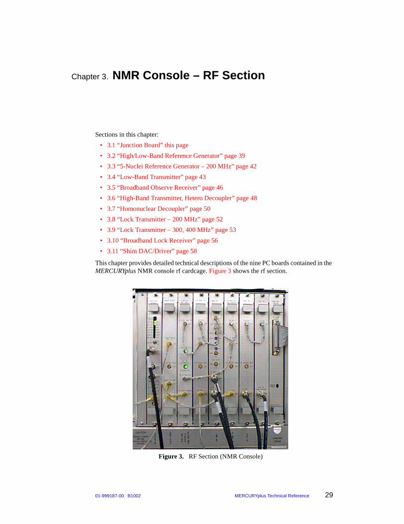
This chapter provides detailed technical descriptions of the nine PC boards contained in the MERCURYplus NMR console rf cardcage. Figure 3 shows the rf section.
Figure 3. RF Section (NMR Console)

Chapter 3. NMR Console – RF Section
30 MERCURYplus Technical Reference 01-999187-00 B1002
3.1 Junction BoardSchematic No. 01-901681-00, Part No. 01-901678-00
The Junction board contains five sections:
• 40-MHz oscillator provides the reference signal throughout the MERCURYplus system and supplies the clock signals to the homo-gate generator, lock-gate generator, and the decoupler modulation frequency generator (DMF) on this Junction board.
• AP bus interface has an analog port (AP) chip and the chip’s input/output buffers, a PAL for data multiplexing, and seven data latches. The latches provide a total of 16 AP-instructions to the various sections on this board and provide DMF and decoupler modulation mode (DMM) information to the DMF generator.
• Gate generator PAL outputs a total of six gates, one synchronization gate, and two blanking signals.
• DMF generator circuit modulates the four quadra-phase signals on the high-speed lines and outputs them to the transmitter boards in the system.
• Safety interlock circuit monitors the system conditions, including over-temperature on the shim DAC, power supply, amplifiers, and low-voltage from the power supply. If the circuit detects any abnormal condition, it provides blanking signals to the power amplifiers and sounds the beeper as an alarm. The system conditions can be read through the AP bus.
Specifications
Table 25 lists Junction board LEDs.
Table 25. Junction Board LEDs
Safety/Alarm Circuit Description Color
DS3 RF power supply green
DS4 Digital power supply green
DS8 SHIM board power supply red
DS5 +28 V/TEMP high-band rf amplifier red
DS6 +28 V/TEMP low-band rf amplifier red
DS7 RF PS temperature red
DS9 ALARM OFF red
AP Interface Description Color
DS2 APSTB green
DS1 APACK green

3.1 Junction Board
01-999187-00 B1002 MERCURYplus Technical Reference 31
Table 26 defines the Junction board P10 and P11 input pins.
Table 26. Junction Board Inputs
P10 Pin Description
High speed lines
C13 HI_BND_TX
C12 HI_BND_90
C11 HI_BND_180
C10 LOW_BND_TX
C9 LOW_BND_90
C8 LOW_BND_180
C7 OBS_RX_GATE
Other lines
A22/C22 HI_BND_TEMP/+28V
A21/C21 LOW_BND_TEMP/+28V
A17 RF_PS_TEMP
C1 Shim board power status, CMOSS/TTL
A30/C30 +24V
A29/C29 –24V
A32/C32 +12V
P11 Pin Description
A13/C13 to A32/C32 AP bus
A10/C10/A11/C11 +5V
A6/C6/A7/C7 –5V

Chapter 3. NMR Console – RF Section
32 MERCURYplus Technical Reference 01-999187-00 B1002
Table 27 shows the Junction board output connections. All signals are CMOS/TTLs except the 40-MHz signals.
Table 27. Junction Board Output
P10 Pin Description
A6 HI_BND_TX_GATE
A10 LOW_BND_TX_GATE
A5 HI_BND_LO_GATE~
A9 LOW_BND_LO_GATE~
A23/C23 HI_BND_BLNKG
A20/C20 LOW_BND_BLNKG
A4 OBS_RX_GATE~
A13 HOMO_TX_GATE (50 kHz)
A1 LOCK_TX_GATE (5 kHz/20 Hz)
A2 LOCK_LO_RX_GATE~ (5 kHz/20 Hz)
C2 Lock_Sync_Out (5 kHz/20 Hz)
A8 HI_BND_90_PM
A7 HI_BND_180_PM
A12 LOW_BND_90_PM
A11 LOW_BND_180_PM
A25/C25 SPINENABLE
C4 ALARM_OUT
BNC/SMB Connectors
Description
J11 LC Aux1
J12 OBS_RX_GATE_SCOPESYNC
J13 LK_LO_RX_GATE~ SCOPESYNC (5 kHz/20 Hz)
J14 LC Aux2
J17 40-MHZ_OUT/STM_BRD, sine wave, 1V to 2Vpp at 50 ohms
J18 40-MHz_TEST, sine wave, 1V to 2Vpp at 50 ohms
J15 T/R SW
P11 Pin Description
A2/C2/A3/C3 40-MHz REF Out, sine wave, 1V to 2Vpp at 50 ohms

3.1 Junction Board
01-999187-00 B1002 MERCURYplus Technical Reference 33
Safety Interlock
The system alarm starts beeping when it senses an over-temperature situation. The Shim DAC board is usually the first board to trigger the alarm. The rf power amplifiers, the main power supply, and finally the digital cardcage supply are next. The spectrometer reboots and the beeper automatically resets to OFF once the power supply returns to acceptable temperature limits. The alarm also can be turned OFF with the alarm switch. Note that the spectrometer will not work unless the alarm switch is ON (in the up position).
Interlocked with the dc power supplies (±12% change) are +5 V (AP bus), +5 V, –5 V, +12 V, +24 V, and –24 V.
Interlocked with the presence/absence of the following signals:
• –28 V, temperature, high-band amplifier
• –28 V, temperature, low-band amplifier
• CMOS/TTL, temperature, rf amp power supply
• CMOS/TTL, Shim board power supply, temperature
• +5 V, alarm off
Typical Power Consumption
AP Bus Buffer (Sheet 1)
U6B and U7B buffer the AP bus signals to the AP_chip U9E. U6G generates strobes to the data latches U9GA, U9GB, U9H, U9J, U9M, U9N, and U9P. Seven data latches are powered on reset to low state by R7, C8, CR1, and U8K. AP chip register 3 ($23) reads the board configuration—SW1 via U5D—or the safety status that is generated by the safety interlock section on the sheet 5. U12G pulse-stretches the AP strobe and AP acknowledge signals and drives the LEDs DS1 and DS2, respectively. U4B buffers the two signals PACK and APDIR from U9E to the AP bus.
40-MHz Reference (Sheet 2)
U2F generates the 40-MHz reference signal that is amplified (by U2D) and split (by U3C, U2W), then output through J17, J18, and P11-A2,C2, A3,C3. The 40-MHz reference signal is also converted to a CMOS/TTL signal by U3H and divided to 5-MHz clock signals by U3J and U3P. U3RB, U3S, and the PAL U3T form a homo decoupler signal generator that generates and outputs the homo transmitter and receiver gate signals. U6T, U6U, and the PAL U6V form a lock gate signal generator that generates the lock transmitter and receiver gate signals.
PAL U6W outputs the lock gate signals and either a constant high (CW) or a constant low (OFF) signal when it receives the input instruction from the AP bus. U6RA and U6RB divide the 5-MHz clock signal to 500 kHz and 2 kHz and U6S, and depending on the fast or slow lock mode, sends one of these clock signals to the lock gate signal generator.
U3RA buffers 5 MHZ_CLK.
+5 V(AP bus), 60 mA +12 V, 10 mA
+5 V, 150 mA +24 V, 400 mA
–5 V, 10 mA –24 V, 10 mA

Chapter 3. NMR Console – RF Section
34 MERCURYplus Technical Reference 01-999187-00 B1002
Decoupler Band Select (Sheet 3)
U12C, U12D, and U12E form a decoupler band-select switch. Only a selected band (either high-band 90/180 phases or low-band 90/180 phases) is connected to the DMF circuit on sheet 4. The PAL U11P generates all the gates and blanking signals. Q2, Q3, Q4, and U12C form a TR switch driver that shifts the voltage from CMOS to +5V and –15V for the TR switch in the high-band preamplifier.
Table 28 shows the 13 output signals, their source, and their conditioning signals and/or instructions.
Table 28. Junction Board Output Signals
Output signal Source Conditioned by
HI_BND_BLNKG OBS_RX_GATE UNBLK_OVRRIDE
HI_BND_CW
HOMO_RX_GATE
OBSRX_TEST_ON
LOW_BND_BLNKG OBS_RX_GATE UNBLK_OVRRIDE
LOW_BND_CW
OBSRX_TEST_ON
HI_BND_LO_GATE~ OBS_RX_GATE OBS_HB/LB~
HOMO_RX_GATE
OBSRX_TEST_ON
LOW_BND_LO_GATE~ OBS_RX_GATE OBS_HB/LB~
OBSRX_TEST_ON
OBS_RX_GATE~ OBS_RX_GATE HOMO_RX_GATE
OBSRX_TEST_ON
HI_BND_TX_GATE HI_BND_TX HI_BND_CW
1.5msec PW Limiter
HB_PW_LMT_OVRDE
LOW_BND_TX_GATE LOW_BND_TX LOW_BND_CW
1.5msec PW Limiter
LB_PW_LMT_OVRDE
PA_GATE/T/R SW OBS_RX_GATE OBS_HB/LB~
HOMO_RX_GATE
OBSRX_TEST_ON
HI_BND_CW
OBS_RX_GATE_SYNC OBS_RX_GATE None
HI_BND_90_PM HI_BND_90 DEC_HB/LB~
DMF Signal
HI_BND_180_PM HI_BND_180 DEC_HB/LB~
DMF Signal
LOW_BND_90_PM LOW_BND_90 DEC_HB/LB~
DMF_Signal
LOW_BND_180_PM LOW_BND_180 DEC_HB/LB~
DMF Signal

3.1 Junction Board
01-999187-00 B1002 MERCURYplus Technical Reference 35
Decoupler Modulation Circuit (Sheet 4)
Sheet 4 shows the decoupler modulation circuit. DMF bits 0 to 18 are designated as the decoupler modulation frequency (DMF) control bits. Bits 19 to 23 are not used.
The DMF generator chip U5M, with U6K and U6N, performs two related functions: to generate a square wave at the DMF frequency and to modulate the 90° and 180° phase lines at that frequency or with a pattern derived from that frequency. DMF is generated by a digital synthesizer inside the DMF generator FPGA. DMM [3:0] selects one of 8 modulation modes (see Table 29).
J11 and J14 output two AP instructions through buffer U9R, LC AUX1 and LC AUX2, respectively.
Comparator (Sheet 5)
The comparator U13LB monitors the dc voltage inputs +24 V and +12 V. The comparators U13M and U13N monitor the dc voltage inputs +5 V, +5 V AP bus and –24 V, –5 V, respectively. These comparators form the voltage window detectors so that if any one of these dc voltages inputs falls off ±12% of their nominal dc voltages, the comparators output a logic-low signal at the test points TP14 and TP15. The logic-low signal at the TP15 drives U13U to sound the beeper LS1 when the switch SW2 is in the normal Alarm_On position. U11W makes the alarm sound broken at a time constant R129*C36. U13T detects glitches on any dc power line and sounds the beeper. The comparator U13P and U13RA are voltage window detectors for the voltages, +28 V, which are fed by high-band and low-band rf amplifiers. If the temperature of either amplifier is too hot, the U13P or U13RA sees 0 V input at P10-A22, C22 or A21, C21, and sends a logic low output at TP15.
Besides the beeper LS1, the display LEDs DS3, DS4, DS5, and DS6 show the conditions of the dc power and rf amplifiers. U11Vs with pin 3 and 11 detect logic changes from the Shim board and the power supplies of the rf amplifiers.These logic changes (condition changes) are also reflected by the beeper and the display LEDs DS7 and DS8. U13V makes an unblanking_override signal that interlocks the rf amplifiers and U6D feeds the system conditions, which can be read through the AP bus. U6D outputs safety status bits by setting the logic on data 7 of the AP register $22. Table 30 lists the safety status bits.
Table 29. Junction Board DMF
0 or 8 = CW
1 or 9 = Square wave
2 or A = FM (a modulator built in the FPGA)
3 or B = External, (not used)
4 or C = Waltz
5 or D = GARP
6 or E = MELV16
7 or F = XY32
Table 30. Safety Status Bits
Safety Status Bits Indicates
READ0 = 0
READ1 = RF PS TEMP
READ2 = SHIM BRD PS
READ3 = LOWBAND RF AMP
READ4 = HIBAND RF AMP
READ5 = DIGITAL PS
READ6 = RF PS
READ7 = ALARM ON

Chapter 3. NMR Console – RF Section
36 MERCURYplus Technical Reference 01-999187-00 B1002
DC Power Inputs (Sheet 6)
Sheet 6 shows the dc power inputs at the back plane connectors, P10 and P11, and two dc voltage regulators. It also power pin information and a list of the bypass capacitors. VR1 (precision voltage regulator) with an external reference voltage device, CR6, and an additional pass transistor, Q1, make the 15-V regulator that supplies the dc power to the 40-MHz reference oscillator. VR2 outputs the regulated +5 V dc voltage using the +24 V dc input voltage. This voltage regulator, used for the safety circuit, is backed up by the +12 V dc input voltage in case the +24 V input voltage fails. CR4 with the voltage divider, R112 and R113, supplies the reference voltages, 2.5 V and 2.0 V, for the voltage comparators in the safety circuit.
PAL _lkgate Inputs and Outputs
Table 31 lists the input and output pin assignments for PAL _lkgate. Note that input signal names terminated with a lowercase “n” are defined as negative true at the IC pin.
Table 31. Junction Board PAL _lkgate Inputs and Outputs
Pin Input Description
1 GATE Gate input, 1 = enabled
2 D0 Data input, positive logic
3 D1 Data input, positive logic
4 D2 Data input, positive logic
5 D3 Data input, positive logic
6 D4 Data input, positive logic
7 D5 Data input, positive logic
8 D6 Data input, positive logic
9 D7 Data input, positive logic
11 ON_OFF Gating on/off, 1 = on
Pin Output Description
13 DONEn Low = done
14 TXn TX gate, low = on
15 RX RX gate, low = off

3.1 Junction Board
01-999187-00 B1002 MERCURYplus Technical Reference 37
PAL _lkoutputs Inputs and Outputs
Table 32 lists the _lkoutputs PAL input and output pin assignments. Note that the input signal names terminated with a lowercase “n” are defined as negative true at the IC pin.
Table 32. Junction Board PAL _lkoutputs Inputs and Outputs
Pin Input Description
4 LKRXG Lock Rx gate
5 LKTXG Lock Tx gate
6 LKRXOFF Test Lock Rx Off, 1=Test
7 LKRXON Test Lock Rx On, 1=Test
8 LKTUNE Lock tune, 1=tune
9 LKTXOFF Test lock Tx Off, 1=Test
Pin Output Description
13 LKTX_GATE Lock Tx gate
14 LKRX_GATEn Lock Lo Rx gate~
15 LKSYNC Lock Sync output
16 LKRXSYNC Lock Lo Rx gate scope sync

Chapter 3. NMR Console – RF Section
38 MERCURYplus Technical Reference 01-999187-00 B1002
PAL _ogates Inputs and Outputs
Table 33 lists the input and output pin assignments of PAL _ogates. Note that input signal names terminated with a lowercase “n” are defined as negative true at the IC pin.
Table 33. PAL _ogates Inputs and Outputs
Pin Input Description
1 UNBLNK_OVR Unblanking override, 1=override
2 HBCW High_Band_CW, 1=CW
3 LBCW Low_Band_CW, 1=CW
4 HBPL_OVR HB_PW_limit_override, 1=override
5 LBPL_OVR LB_PW_limit_override, 1=override
6 OBS_HL OBS_Hi_Band/Low_Band, 1=HiBand
7 HOMO_RGn Homo_RX_Gate
8 HDEC_ON Homo_decoupler_On/Off, 1=On.
9 RX_TEST OBS_RX_Test_On, 1=test
10 HBTX Hi_Band_TX_Gate
11 LBTX Low_Band_TX_Gate
13 RCVRGATEn RX_Gate
14 LBTX_PWL Low_Band_PW_Limit
23 HBTX_PWL Hi_Band_PW_Limit
Pin Output Description
15 PA_GATE Preamp_Gate
16 RX_GATEn
17 HBLOn Hi_Band_LO_Gate
18 LBLOn Low_Band_LO_Gate
19 LBTXG Low_Band_TX_Gate_Out
20 HBTXG Hi_Band_TX_Gate_Out
21 LBBLNKGn Low_Band_Blanking, 1=Unblank
22 HBBLNKGn Hi_Band_Blanking, 1=Unblank

3.2 High/Low-Band Reference Generator
01-999187-00 B1002 MERCURYplus Technical Reference 39
PAL addrmux Inputs and Outputs
Table 34 lists the input and output pin assignments for the addrmux PAL. Note that the input signal names terminated with a lowercase “n” are defined as negative true at the IC pin.
3.2 High/Low-Band Reference GeneratorThe High/Low-Band Reference Generator board has three versions, depending on the frequency of the system.
This board generates the reference rf signals used by the HI BND TX HET DCPLR, LOW BND TX and HOMODECOUPLER. The reference generator supplies all the reference signal frequencies to observe 15N to 31P and 19F/1H nuclei. A reduced-capability board (the 4-Nuclei Reference Generator board), supporting only 4 nuclei, is also available for the 200- and 300-MHz systems and can be used in place of the High/Low-Band Reference Generator board.
System 200 MHz 300 MHz 400 MHz
Schematic No. 01-901552-00 01-907839-00 01-907841-00
Part No. 01-993948-01 00-993948-50 00-993948-52
Table 34. PAL addrmux Inputs and Outputs
Pin Input Description
1 A0 Address inputs
2 A1 Address inputs
3 A2 Address inputs
4 A3 Address inputs
5 A4 Address inputs
6 A5 Address inputs
7 A6 Address inputs
8 A7 Address inputs
9 STB Data strobe
Pin Output Description
19 LS1 8-bit latch strobe 1
18 DACENn DAC enable
17 HOP HOP PLL
16 AW AWR PLL
15 MW MWR PLL
20 DDSn WR DDS
21 DMM Added strobo for DMM
Chapter 3. NMR Console – RF Section
40 MERCURYplus Technical Reference 01-999187-00 B1002
Block Diagram (Sheet 8)
U1, 2, 3, 5, and 9 make up the AP bus interface section. PAL U6 generates strobes to latch data into various devices.
The 40-MHz reference signal enters P31–2, 3 and is converted to an ECL signal by U10 and feeds the reference input of the digital phase detector U11. U87 converts the 40-MHz signal to a CMOS/TTL level. U11, U12, U13, and U14 make up a PLL phase-locked loop system, that generates a fixed 360-MHz reference signal at the output of splitter U17. U12 and associated components make up the PLL loop filter. U14 is the VCO signal divide-by-9 IC and feeds the VCO input of phase detector U11.
U30, U31, U32, and U38 make up the Low BND PLL system. U30 and U38 are VLSI phase locked loop ICs containing two programmable dividers and a digital phase detector.
U30 is used as a VCO divider, ÷V, and phase detector. The ÷V can be programmed to divide by 90 to 1295. Its internal reference divider, ÷R, is set to ÷1 in this application.
U38 is only used as a PLL system reference divider, ÷R, programmable to divide by 90 to 1295.
The U32 VCO output signal frequency at test point 26 is obtained as follows:
For example, the 31P VCO signal frequency is obtained:
200-MHz system:
300-MHz system:
400-MHz system:
The VCO signal out of FL3, REF L.O. drives the L.O. of the down-converter mixer U94; its level is adjusted by RV2. The 360-MHz reference signal is applied to the rf input of U94.
The difference signal, FVCO – 360 MHz, is amplified and filtered by U91, U92, and FL7, FL8. The LOW BND REF GEN signal is available at J34 and its level adjusted by RV7.
In this example, the 31P REF GEN signal is obtained as follows:
200-MHz system:
300-MHz system:
F31P = 492.110 MHz – 360 MHz = 132.110 MHz
400-MHz system:
The process of down-converting reduces the spurious mixer products within the band of required output frequencies.
The HI BND REF GEN section on this board is composed of the U80, U81, and U82 PLL system. Only one PLL device is used, U80. The ÷V programmable VCO divider has a range of 90 to 1295, and the reference divider ÷R has a range of 1 to 16. A 20-MHz reference
Fvco360MHzRnumber------------------------ Vnumber×=
Fvco360MHz
106---------------------- 133× 451.6MHz= =
Fvco360MHz
109---------------------- 149× 492.1MHz= =
Fvco360MHz
96---------------------- 142× 532.5MHz= =
F31
P 451.698 MHz 360 MHz– 91.698 MHz= =
F31
P 532.500 MHz 360 MHz– 172.500 MHz= =

3.2 High/Low-Band Reference Generator
01-999187-00 B1002 MERCURYplus Technical Reference 41
signal from U85 is used in this setup because the HI BND REF GEN signal is not generated by down conversion.
The U82 VCO output signal is amplified by U83, split by U84, amplified and filtered by U93, FL6, and split by U95.
The HI BND REF GEN signal is available at J37, which feeds the Homo Decoupler board, and J36, which feeds the High Band Transmitter board. The signal level is adjusted by RV9. As an example, the 1H REF GEN signal is obtained as follows:
200-MHz system:
300-MHz system:
400-MHz system:
Most nuclei observe frequencies can be obtained within ±150 kHz of the resonance frequency by programming the ÷R and ÷V dividers. The error can be offset by adjusting the TXOFFSET frequency on the transmitter boards.
The PLL ICs also contain a “locked” indicator circuit, which controls a “locked” LED (U88, DS1, DS2). Due to the wide PLL frequency range, the LED can indicate a locked condition, but the VCO frequency can be wrong because of incorrect ÷V and ÷R program numbers.
Each PLL system contains a LC low-pass filter, L10, L24, and L11. These filters reduce the phase detector frequency sidebands at the output of the VCOs in the 1.2 MHz and higher frequency range.
Input
Input signals (200-, 300-, 400-MHz):
• P31–2, 3: Sine wave, 40-MHz reference, 1 to 2 Vpp at 50 ohms
• P31: AP bus, CMOS/TTL
Typical power consumption:
Output
Output signals:
200-MHz system:
• J34: LOW BND REF GEN OUT, 15N – 31P 30-92 MHz, +2.5 to +3.8 dBm
• J36, J37: HI BND REF GEN OUT, 1H = 210.769 MHz, 19F = 198.750 MHz, +2.5 to +3.8 dBm
300-MHz system:
• J34: LOW BND REF GEN OUT, 15N – 31P 40-133 MHz, +2.5 to +3.8 dBm
+5 V, 1.26 A +24 V, 90 mA
+12 V, 370 mA –24 V, 15 mA
F H1 20MHz
13------------------- 137× 210.8MHz= =
F H1 20MHz
13------------------- 202× 310.8MHz= =
F H1 20MHz
15------------------- 308× 410.7MHz= =

Chapter 3. NMR Console – RF Section
42 MERCURYplus Technical Reference 01-999187-00 B1002
• J36, J37: HI BND REF GEN OUT, 1H = 310.769 MHz, 19F = 292.857 MHz, +2.5 to +3.8 dBm
400-MHz system:
• J34: LOW BND REF GEN OUT, 15N – 31P 50-173 MHz, +2.5 to +3.8 dBm
• J36, J37: HI BND REF GEN OUT, 1H = 410.667 MHz, 19F=387.143 MHz, +2.5 to +3.8 dBm
3.3 5-Nuclei Reference Generator – 200 MHzThe 5-Nuclei Reference Generator board has two versions:
This board generates the reference rf signals used by the HI BND TX HET DCPLR, LOW BND TX and HOMODECOUPLER. The reference generator supplies all the reference signal frequencies to observe 2H,13C, 31P, and 19F/1H nuclei. The 5-Nuclei Reference Generator board is a cost-reduced version of the High/Low-Band Reference Generator board, offering only 5-nuclei observation and is available only for 200- and 300-MHz systems.
Note: Observation of 2H is only available for automated deuterium gradient shimming.
Block Diagram (Sheet 6)
U1, 2, 3, 5, and 9 make up the AP bus interface section. PAL U6 generates strobes to latch data into various devices.
The 40-MHz reference signal enters P31–2, 3 and is converted into a CMOS/TTL signal by U87, test point 56. U85 divides this signal by 2 and feeds the reference input of the U80 PLL IC, test point 54. U80, U81, and U82 make up the 19F/1H PLL system. U80 is a VLSI phase-locked loop IC containing two programmable dividers and a digital phase detector. U81 and associated components make up the loop filter. L11, a low-pass filter, reduces phase detector sidebands in the 1.2 MHz and higher frequency range. The U82 VCO output is buffered by U83 and the signal is split by U84. One channel feeds the VCO divider of U80, test point 55. The other channel provides the 19F/1H reference signal output at J36 and J37. The U82 VCO signal frequency is obtained as follows:
For example, the 1H VCO signal frequency is obtained:
200-MHz system:
300-MHz system:
System 200 MHz
Schematic No. 01-905853-00
Part No. 01-905856-51
fvco20MHz
Rnumber------------------------ Vnumber×=
fvco20MHz
13------------------- 137× 210.769MHz= =
fvco20MHz
13------------------- 202× 310.769MHz= =

3.4 Low-Band Transmitter
01-999187-00 B1002 MERCURYplus Technical Reference 43
U30, U31, and U32 make up the 2H/13C/31P PLL system. U30 is the same VLSI phase-locked loop IC as U80. The 10-MHz reference signal at test point 20 is applied to the U30 reference input. Note this reference signal is jumper selected by JMP1.
The 200-MHz NMR system uses 10 MHz as a U30 PLL reference signal because the ÷R is only programmable from 1 to 16. The U32 VCO output signal is buffered by U33 and split by U34. One channel feeds the VCO divider of U30, test point 21. The other channel is amplified by U92 and filtered with the selectable lowpass filters FL8 and FL9. The 2H/13C/31P Ref Gen signal is available at J34.
Both PLL ICs, U80 and U30, contain a lock detector, U88, which activates DS1 and DS2 LEDs. Due to the wide PLL frequency range, the LED can indicate a locked condition, but the VCO frequency can be wrong due to the incorrect ÷V and ÷R program numbers.
Input
Input signals:
• P31–2, 3: Sine wave, 40-MHz reference, 1 to 2 Vpp at 50 ohms
• P31: AP bus, CMOS/TTL
Typical power consumption:
Output
Output signals:
200-MHz system:
• J34: LOW BND REF GEN OUT, 2H = 41.333 MHz, 13C = 61.0 MHz, 31P = 91.666 MHz, +2.5 to +3.8 dBm
• J36, J37: HI BND REF GEN OUT, 1H = 210.769 MHz, 19F = 198.750 MHz, +2.5 to +3.8 dBm
300-MHz system:
• J34: LOW BND REF GEN OUT, 2H = 56.667 MHz, 13C = 86 MHz, 31P = 132 MHz, +2.5 to +3.8 dBm
• J36, J37: HI BND REF GEN OUT, 1H = 310.769 MHz, 19F = 292.857 MHz, +2.5 to +3.8 dBm
3.4 Low-Band TransmitterThe Low-Band Transmitter board has three versions.
+5 V, 790 mA +24 V, 70 mA
+12 V, 200 mA –24 V, 15 mA
System 200 MHz 300 MHz 400 MHz
Schematic No. 01-901550-00 00-992845-00 01-902195-00
Part No. 00-992842-07 00-992842-06 00-992842-08

Chapter 3. NMR Console – RF Section
44 MERCURYplus Technical Reference 01-999187-00 B1002
This board generates the gated 15N thru 31P observe signals, including quadrature phase modulation. The L.O. and transmitter signal frequencies are nominal for all systems. The actual frequencies depend on the magnet setting and can be slightly higher or lower.
The output signals are related as follows:
200-MHz system:
• 15N-31P: L.O. = LOW BND REF GEN = 30.968 to 91.698 MHz
• 15N-31P: TX = L.O.–TXOFFSET = 20 to 82 MHz
300-MHz system:
• 15N-31P: L.O. = LOW BND REF GEN = 40.5 to 132.8 MHz
• 15N-31P: TX = L.O.–TXOFFSET = 30 to 122 MHz
400-MHz system:
• 15N-31P: L.O. = LOW BND REF GEN = 51.081 to 172.5 MHz
• 15N-31P: TX = L.O.–TXOFFSET = 40 to 162 MHz
All systems:
• 15N -31P: TX OFFSET = 10.5 to 10.8 MHz
The Obs Rx detector reference signal is exactly the same frequency as the TX OFFSET signal, because the same data is used on both DDS channels.
Block Diagram (Sheet 6)
U1, 2, 3, 4, 5, 9 make up the AP bus interface section. PAL U6 generates strobes to latch data into various devices and data latch U7.
The 40-MHz reference signal enters P41–2, 3 and is converted to a CMOS/TTL signal by U24. This clock is applied to the DDS IC, U15. U15 is a VLSI direct digital synthesizer containing two identical sections. The DDS is composed of an input data and control section (32 bits), an accumulator section, and a sine PROM. Its output feeds DACs U16 and U17. After filtering FL1, 2 and FL13, 5 a clean 10.5 to 10.8-MHz sine wave signal is available. The frequency step resolution is 40 MHz/32 bits = 0.0093 Hz. This device also contains a phase-shift control function. In this application, the resolution is 360°/8 bits = 1.4°. A fast quadrature modulation is also available by the PMCLK GEN, (U70, U71, and U72) clocking the 90° and 180° lines, P40–11, 12 into U15. The PMCLK GEN generates a 100-ns positive pulse on every 90°/180° line transition.
The 10.5 to 10.8-MHz signal at P40–14 is fed to the OBS RX phase detector via the rf backplane.
The 10.5 to10.8-MHz signal at the output of FL5 is amplitude-controlled by U46, having a total range of 48 dB and an 8-bit resolution, DAC U8. The output of U46 is further amplified and filtered by U47 and FL6 and is fed to the SSB mixer, U41, 42, 43, 48, and 49. RV5 sets the output power of the transmitter signal at J43.
The LOW BND REF GEN signal enters J44 and is amplified by U51 and split by U40. One channel is gated by U50, amplified by U44, and drives the L.O. of the SSB mixer. The second channel is gated and amplified by U60, 61, 62 and U66. The observe L.O. is available at J42 with its level set by RV2.
The lower sideband output of the SSB mixer is gated and amplified by U63, 64, 65 and U67, 68. The transmitter signal is available at J43. U52 and U53 make up a switchable 20-dB attenuator section, to increase the TX attenuation to 68 dB.
3.4 Low-Band Transmitter
01-999187-00 B1002 MERCURYplus Technical Reference 45
Input
Input signals:
200-MHz system:
• J44: LOW BND REF GEN IN, 30 to 92 MHz, +3 dBm, ±0.3 dB
300-MHz system:
• J44: LOW BND REF GEN IN, 40 to 133 MHz, +3 dBm, ±0.3 dB
400-MHz system:
• J44: LOW BND REF GEN IN, 50 to 173 MHz, +3 dBm, ±0.3 dB
All systems:
• P41–2, 3: Sine wave, 40-MHz reference, 1 to 2 Vpp at 50 ohms
• P41: AP Bus, CMOS/TTL
• P40–11,12: QUAD PHASE HSP lines, CMOS/TTL
• P40–9,10: L.O. GATE and TX GATE, CMOS/TTL
Typical power consumption:
Output
Output signals:
200-MHz system:
• J42: 15N– 31P, 30.968 to 91.698 MHz, L.O. out, 0 to +2 dBm
• J43: 15N– 31P, 20 to 82 MHz TX out, +1 to +4 dBm, attenuation range of 68 dB
300-MHz system:
• J42: 15N– 31P, 40.5 to 132.8 MHz, L.O. out, 0 to +2 dBm
• J43: 15N– 31P, 30 to 122 MHz TX out, +1 to +4 dBm, attenuation range of 68 dB
400-MHz system:
• J42: 15N– 31P, 51.081 to 172.5 MHz, L.O. out, 0 to +2 dBm
• J43: 15N– 31P, 40 to 162 MHz TX out, +1 to +4 dBm, attenuation range of 68 dB
All systems:
• J45: TX OFFSET: 10.5 to 10.8 MHz, –10 dBm typ. Freq/Phase test
• P40–14: Obs RX detector reference, 10.5 to 10.8 MHz, +1 to +3 dBm
• JT1: Obs RX reference, 10.5 to 10.8 MHz, Freq/Phase test
+5 V, 300 mA +24 V, 20 mA +12 V, 300 mA
–5 V, 370 mA –24 V, 15 mA

Chapter 3. NMR Console – RF Section
46 MERCURYplus Technical Reference 01-999187-00 B1002
3.5 Broadband Observe ReceiverThe Broadband Observe board has three versions:
This board down converts and phase/amplitude detects the 15N to 1H NMR observe signal of the system. The L.O. signal frequencies are nominal for all systems. The actual frequencies depend on the magnet setting and can be slightly higher or lower. The board outputs are the quadrature observe signals 0° and 90°, which are filtered by a 1 to 25 kHz programmable, fourth-order, low-pass Butterworth filter, and a fixed 55-kHz fourth-order, low-pass, Butterworth filter.
Block Diagram (Sheet 7)
U1, U2, U3, U4, and U5 make up the AP bus interface section. PAL U6 generates strobes to latch the data into various devices, data latch U7, DAC U8, U40 and U41 filters. The observe HIBND L.O. enters J52 and the LOW BND L.O. at J53. Relay K2 selects which band of nuclei is to be observed. The L.O. signal is amplified by U21 and drives the IRM (image reject mixer) L.O. inputs U25, U26, through U23, U24, and K5. The NMR observe signal from the broadband preamps enter the receiver at J54, HIBND and J55, LOWBND. K1 selects the observe band. These inputs also provide a +12 V supply for the observe preamps. The ability to select the HI and LOWBND NMR observe signals enables the system to provide indirect detection with, 1H observe and 13C decoupling.
The observe signals are amplified by U15, gated by U16, U17, and enter the IRM at U22, which–with U23, U24, U25, U26, and U27–makes up the IRM. The output is the 10.5 to 10.8-MHz IF signal, Flo–Ftx. This IRM suppresses the upper rf sideband, Frf + 2 x (10.5 to 10.8 MHz). Since the preamp is wideband, this upper sideband carries only thermal noise. Its suppression improves the system signal to noise by up to 40%. Test point 15 is used to confirm the proper suppression, typically 20 to 30 dB. U23 and U24, 90° splitters, have a limited bandwidth. These 20- and 30-MHz HP filters reduce any 10.5 to 10.8 MHz spurious signals, which can leak into the 10.65 MHz IF channel and suppress the switching spikes when homo decoupling is used.
The IF signal is amplified by U30, U10, U31, and U32. RV8 adjusts the total receiver gain to within ± 1 dB. The IF gain is approx. 47.5 dB max. and can be reduced by up to 39 dB by K8 and K7, and 9 dB by U32. FL1 is the 10.5 to 10.8-MHz IF filter, having a –3 dB bandwidth of about. 4 MHz and is flat from 10.4 to 10.9 MHz. DAC U8 controls the variable gain amplifier U32. The DAC is set up to obtain 1-dB step attenuation. The K10, 0/–10 dB attenuator is only used in the HI BND mode to increase the dynamic range of the receiver.
The IF signal enters the quadrature phase/amplitude detector U36. The Obs RX detector reference signals, 10.5 to 10.8 MHz, enter P50-19, HIBND and P50-14, LOWBND, are amplified by U33, and drive the L.O. input of U36.
The quadrature (90°) demodulated NMR signal exits U36 through a 300-kHz low-pass filter and is amplified by U37, 0° OBS, and U38, 90° OBS. These two channels feed the programmable 1 to 25-kHz low-pass filters U40 and U41, which are monolithic filters, fourth-order types. The channels also feed the discrete active 55-kHz, fourth-order, low-pass filters U51 and U52. This filter is mainly used to observe the 19F nucleus. The RV5
System 200 MHz 300 MHz 400 MHz
Schematic No. 01-905762-00 01-905753-00 01-905764-00
Part No. 01-905750-01 01-905750-00 01-905750-02

3.5 Broadband Observe Receiver
01-999187-00 B1002 MERCURYplus Technical Reference 47
and RV6 null the DC offset of this filter, and RV7 balances the gain. A fourth order filter has an attenuation slope of approximately 80 dB.
The K9 relay selects which filter ranges are to be used on each channel. U42 and U43 provide further amplification. The observe signals exit the board in a differential mode at P50-A, C12 and P50-A, C10. These signals are also available at the board front panel, J58 and J59, for test and dc offset adjustments. The RV3 and RV4 null the dc offset of the 1 to 25-kHz filter sections, and RV2 balances the gain. These adjustments are critical and adjustable from the front panel. RV1 adjusts the 90° quadrature detectors for exactly 90° via the varicap diode CR13 from the front panel and also compensates for phase shifts generated by the filters. These adjustments reduce NMR signal images and the center spike in the spectra. RV10 and RV11 compensate for the DC offset at the Quad detector U36 output, which can vary from 0.1 mV to 5 mV, and is due to the L.O. rectification of the mixers.
The circuit between TP10 and TP9 contains a 3µs delay section need to prevent T/R switching spikes from entering the OBS RX, (OBS RX GATE, 3µs ON delay)
Input
Input signals:
All systems:
• P51: AP bus, CMOS/TTL
• P50-A,C19: HIBND OBS RX reference 10.5 to 10.8 MHz, +2 dBm ±1dB.
• P50-A,C14: LOWBND OBS RX reference, 10.5 to 10.8 MHz, +2 dBm, ±1dB.
• P50-A,C4: OBS RX gate, CMOS/TTL
Typical power consumption:
Output
Output signals:
• P50-A,C12: OBS 0° Out, differential, 5 Vpp, RL = 2 kohm, dc to 50 kHz
• J59: OBS 0° Out, test
Input signal
Definition200-MHz System
300-MHz System
400-MHz System
Tolerance/range
J54 HIBND Preamp Signal In
200.057, 188.220
300.075, 282.322
400.050376.381
1H/19F −66 to −27 dBm
J55 LOWBND Preamp Signal In
20.280 to 80.984
30.419 to 121.472
40.553 to 161.943
15N-31P −66 to −27 dBm
J52 HIBND L.O. In 210.769, 198.750
310.769 292.857
410.667 387.143
0 dBm, ±1dB.
J53 LOWBND L.O. In
30.968 to 91.698
41.053 to 132.110
51.081 to 172.500
0 dBm, ±1dB.
+5 V, 340 mA, all relays energized +24 V, 320 mA
+12 V, 70 mA –24 V, 70 mA

Chapter 3. NMR Console – RF Section
48 MERCURYplus Technical Reference 01-999187-00 B1002
• P50-A,C10: OBS 90° Out, differential, 5 Vpp, RL = 2 kohm, dc to 50 kHz
• J58: OBS 90° Out, test
General specifications include:
• Total maximum Rx gain, Preamp In J54, J55 to 0°/ 90° OBS Out P50-12, P50-10: 84 dB ±1 dB. Note: 5 Vpp is equivalent to +18 dBm, 50-ohm load.
• Signal attenuation range: 20 dB, 10 dB, 0 dB to 9 dB additive, ±2 dB, total attenuation, monotonic, 1 dB, ±0.5 dB.
3.6 High-Band Transmitter, Hetero DecouplerThe High-Band Observe Transmitter board has three versions:
This board generates the gated 1H and 19F observe signals and also serves as a CW or phase-modulated 1H hetero decoupler. The L.O. and transmitter signal frequencies are nominal for all systems. The actual frequencies depend on the magnet setting and can be slightly higher or lower.
The output signals are related as follows:
200-MHz system:
• 1H: L.O. = HI BND REF GEN = 210.769 MHz; TX = L.O.–TXOFFSET = 200.057 MHz; TXOFFSET = 10.5 to 10.8 MHz, nominal
• 19F: L.O. = HI BND REF GEN = 198.750 MHz;TX = L.O.–TXOFFSET = 188.220 MHz;TXOFFSET = 10.5 to 10.8 MHz, nominal
300-MHz system:
• 1H: L.O. = HI BND REF GEN = 310.769 MHz;TX = L.O.–TXOFFSET = 300.075 MHz;TXOFFSET = 10.5 to 10.8 MHz, nominal
• 19F: L.O. = HI BND REF GEN = 292.857 MHz;TX = L.O.–TXOFFSET = 282.322 MHz;TXOFFSET = 10.5 to 10.8 MHz, nominal
400-MHz system:
• 1H: L.O. = HI BND REF GEN = 410.667 MHz;TX = L.O.–TXOFFSET = 400.050 MHz;TXOFFSET = 10.5 to 10.8 MHz, nominal
• 19F: L.O. = HI BND REF GEN = 387.143 MHz;TX = L.O.–TXOFFSET = 376.381 MHz;TXOFFSET = 10.5 to 10.8 MHz, nominal
The OBS RX detector reference signal is exactly the same frequency as the TXOFFSET signal, since the same data is used on both DDS channels.
System 200 MHz 300 MHz 400 MHz
Schematic No. 01-901548-00 00-992849-00 01-902191-00
Part No. 00-992846-04 00-992846-03 00-992846-05

3.6 High-Band Transmitter, Hetero Decoupler
01-999187-00 B1002 MERCURYplus Technical Reference 49
Block Diagram (Sheet 6)
U1, 2, 3, 4, 5, 9 make up the AP bus interface section. PAL U6 generates strobes to latch data into various devices and data latch U7.
The 40-MHz reference signal enters P61–2, 3 and is converted to a CMOS/TTL signal by U24. This clock is applied to the DDS IC, U15. U15 is a VLSI direct digital synthesizer containing two identical sections. The DDS is basically composed of an input data and control section (32 bits), an accumulator section, and a sine PROM. Its output feeds the DACs U16 and U17. FL1, FL2, FL13, and FL5 filters provide a clean 10.5 to 10.8-MHz sine wave signal. The frequency-step resolution is 40 MHz/32 bits = 0.0093 Hz. This device also contains a phase shift control function and, in this application, the resolution is 360°/8 bits = 1.4×°. A fast quadrature modulation is also available by the PMCLK GEN, (U70, U71, and U72) clocking the 90° and 180° lines, P40–11, 12 into U15. The PMCLK GEN generates a 100-ns positive pulse on every 90°/180° line transition.
The 10.5 to 10.8-MHz signal at P60–19 is fed to the OBS RX phase detector via the rf backplane.
The 10.5 to 10.8-MHz signal at the output of FL5 is amplitude controlled by U46, having a total range of 48 dB and an 8-bit resolution, DAC U8.
The output of U46 is further amplified and filtered by U47 and FL6, which feeds the SSB MIXER, U41, 42, 43, 48, 49. RV5 sets the output power of the transmitter signal at J63.
The HI BND REF GEN signal enters J66, amplified by U51, and split by U40. One channel is gated by U50, amplified by U44, and drives the L.O. of the SSB mixer. The second channel is gated and amplified by U60, 61, 62 and U66. The observe L.O. is available at J62 and its level set by RV2.
The lower sideband output of the SSB mixer is gated and amplified by U63, 64, 65 and U67, 68. The transmitter signal is available at J63. U100 and 101 make up a fast programmable 30-dB attenuator, which is used to extend the total TX attenuation range to 78 dB and provide fast amplitude modulation.
Input
Input signals:
All systems
• P61–2, 3: Sine wave, 40-MHz reference, 1 to 2 Vpp at 50 ohms
• P61: AP bus, CMOS/TTL
• P60–7, 8: QUAD PHASE HSP lines, CMOS/TTL
• P60–5, 6: L.O. GATE and TX GATE, CMOS/TTL
Typical power consumption:
Input Signal
Definition200-MHz System
300-MHz System
400-MHz System
Tolerance
J66 HIBND REF GEN IN
210.769 198.750
310.769292.857
410.667387.143
+3 dBm, ±0.3 dB
+5 V, 300 mA +24 V, 15 mA +12 V, 290 mA
–5 V, 370 mA –24 V, 15 mA

Chapter 3. NMR Console – RF Section
50 MERCURYplus Technical Reference 01-999187-00 B1002
Output
Output signals:
200-MHz system:
• J62: 1H, 19F, 210.769 MHz, 198.750 MHz, L.O. out, 0 to +2 dBm
• J63: 1H, 19F, 200.057 MHz, 188.220 MHz TX out, +1 to +3 dBm, attenuation range of 78 dB
300-MHz system:
• J62: 1H, 19F, 310.769 MHz, 292. 857 MHz, L.O. out, 0 to +2 dBm
• J63: 1H, 19F, 300.075 MHz, 282.322 MHz TX out, +1 to +3 dBm, attenuation range of 78 dB
400-MHz system:
• J62: 1H, 19F, 410.667 MHz, 387.143 MHz, L.O. out, 0 to +2 dBm
• J63: 1H, 19F, 400.050 MHz, 376.381 MHz TX out, +1 to +3 dBm, attenuation range of 78 dB
All systems:
• J65: TX OFFSET: 10.5 to 10.8 MHz, –10 dBm typ. Freq/Phase test
• P60–19: Obs RX detector reference, 10.5 to 10.8 MHz, +1 to +3 dBm
• JT1: Obs RX reference, 10.5 to 10.8 MHz, Freq/Phase test
3.7 Homonuclear DecouplerThe Homonuclear Decoupler board generates the gated 1H homo decoupler signal. There are three versions of this board depending on the magnet proton frequency:
The output signals are related as follows:
The transmitter signal frequencies are nominal for all systems. The actual frequencies depend on the magnet setting and can be slightly higher or lower.
This board does not provide observe L.O. or observe RX detector reference signal outputs.
Block Diagram (Sheet 6)
U1, 2, 3, 4, 5, 9 make up the AP bus interface section. PAL U6 generates strobes to latch data into various devices and data latches U7.
System 200 MHz 300 MHz 400 MHz
Schematic No. 01-901549-00 00-992873-00 01-902193-00
Part No. 00-992870-07 00-992870-06 00-992870-08
System 200 MHz 300 MHz 400 MHz Tolerance
1H HOMOTX =HI BND REF GEN–TXOFFSET = 200.057 300.075 400.050 MHz
TXOFFSET = 10.650 10.650 10.650 MHz nominal

3.7 Homonuclear Decoupler
01-999187-00 B1002 MERCURYplus Technical Reference 51
The 40-MHz reference signal enters P21–2, 3 and is converted to a CMOS/TTL signal by U24. This clock is applied to the DDS IC, U15. U15 is a VLSI direct digital synthesizer containing two identical sections. The Qualcomm DDS is composed of an input data and control section (32 bits), an accumulator section, and a sine PROM. The DDS output feeds DAC U16. A clean 10.5 to 10.8-MHz sine wave signal is available after filtering with FL13 and FL5. The frequency step resolution is 40 MHz/32 bits = 0.0093 Hz.
The 10.5 to 10.8-MHz signal at the output of FL5 is amplitude-controlled by U46 and has a total range of 48 dB and DAC U8 gives an 8-bit resolution.
The output of U46 is further amplified and filtered by U47 and FL6, feeding the SSB mixer, U41, 42, 43, 48, 49. RV5 sets the output power of the homo decoupler at J23.
The HI BND REF GEN signal enters J27 and is amplified by U51 and gated by U50. U44 amplifies the U50 output and drives the L.O. of the SSB mixer. The L.O. level is adjusted by RV2.
The lower sideband output of the SSB mixer is attenuated by a programmable attenuator AT1 with a range of 0 to 35 dB in 5-dB steps and is then gated by U70, 73, 74, amplified by U71, U72, and filtered by FL11 and FL12.
This homo decoupler signal is fed to a directional coupler U76 and is available at J23.
The HI BND Obs TX signal enters at J28 and exits at J23 with the homo decoupler signal.
The rf gates U73 and U74 have a slower rise and fall time, approximately 0.5 µs, in order to reduce homo decoupler spikes in the observe channel.
Input
Input signal specifications by system:
Input signals for all systems:
• P21–2, 3: Sine wave, 40-MHz reference, 1 to 2 Vpp at 50 ohms
• P21: AP BUS, CMOS/TTL
• P20–13: HOMO TX GATE, CMOS/TTL
Typical power consumption:
Output
The output signal frequency listed by system.
Input Signals
Definition200-MHz System
300-MHz System
400-MHz System
Tolerance
J27 HI BND REF GEN IN 210.769 310.769 410.667 +3 dBm ± 0.3 dB
J28 HI BND TX IN 200.057 300.075 400.050 +1 dBm ± 0.3 dB
+5 V, 190 mA +24 V, 10 mA +12 V, 220 mA
–5 V, 200 mA –24 V, 10 mA
Output Signal
Definition200-MHz System
300-MHz System
400-MHz System
Tolerance

Chapter 3. NMR Console – RF Section
52 MERCURYplus Technical Reference 01-999187-00 B1002
Output signal for J25 on all systems: TX OFFSET: 10.5 to 10.8 MHz, –10 dBm typical
3.8 Lock Transmitter – 200 MHzSchematic No. 01-901557-00, Part No. 01-901554-02
The 200-MHz Lock Transmitter board generates the gated L.O. and TX signals and lock receiver detector reference signal for the 200-MHz system. The L.O. and transmitter signal frequencies are nominal for all systems. The actual frequencies depend on the magnet setting and can be slightly higher or lower. The 200-MHz system lock transmitter uses a different board than is used for the 300 and 400 systems, but the transmitter functions the same. The main difference is that no phase lock loop required for the 200-MHz board.
The output signals are related as follows:
• L.O. = 40 MHz REF ÷ 2 = 20 MHz
• TX = L.O. + TXOFFSET = 30.710 MHz
• TX OFFSET range = 10.5 to 10.8 MHz, nominal.
The Lock receiver detector reference signal is exactly the same frequency as the TX OFFSET signal, because the same data is used on both DDS channels.
Block Diagram (Sheet 8)
U1, U2, U3, U4, U5, and U9 make up the AP bus interface section.
PAL U6 generates strobes to latch data into various devices and data latch U7.
The 40-MHz reference signal enters P71-2, 3 and is converted to a CMOS/TTL signal by U24. This clock is applied to the DDS IC, U15. U15 is a VLSI direct digital synthesizer containing two identical sections. This DDS is composed of an input data and control section (32 bits), an accumulator section, and a sine PROM. This device also includes a phase-shift function (8 bits), which allows the TX OFFSET signal to be phase shifted by 1.4° and is controlled by software data. This function is needed to adjust the phase of the NMR lock system. The DDS outputs feed the DACs U16 and U17. A clean 10.5 to 10.8-MHz signal is available after filtering with FL1, FL2, FL13, and FL5. The frequency step resolution is 40 MHz/32 bits = 0.0093 Hz. A fast quadrature phase modulation is also available, but is not used on this board. A 5-MHz clock, U35, 36, enables this fast quadrature phase modulation. The PM1, 2 EXT BIT are all hardwired to ground. This enables setting fast quadrature-phase modulation to an initial zero phase-shift value.
The 10.5 to 10.8-MHz signal at P70- 19 is fed to the lock Rx phase detector via the rf backplane. The 10.5 to 10.8 MHz at the output of FL5 is amplitude controlled by U46, having a total range of 48 dB and an 8-bit resolution, DAC U8. The output of U46 is further amplified and filtered by U47 and FL6 and feeds the DBM (double balanced mixer) U42. The RV5 sets the output power of the transmitter signal at J73.
The L.O. is generated by dividing the 40-MHz reference signal by 2 using U35 and is buffered by U37. This 20-MHz signal is amplified by U70, filterd by FL7, and split by U40.
One channel is gated by U50, amplified by U44, and drives the L.O. of mixer U42.
J23 1H, HI BND, TX out 200.057 300.075 400.050 +0 dBm, ± 0.5 dB
HOMO DCPLR TX OUT, attenuation range of 83 dB
200.057 300.075 400.050 −13 dBm, ±1 dB

3.9 Lock Transmitter – 300, 400 MHz
01-999187-00 B1002 MERCURYplus Technical Reference 53
The second channel, L.O.1, is gated, amplified, and filtered by U60, U75, U61, U62 and FL10. The L.O. exits the board at J72, and RV2 adjusts the level.
The upper sideband (USB), 30.71 MHz, out of mixer U42 is amplified and filtered by U51 and FL14. The U63 switch is used as a switchable attenuator, 15 dB net. This attenuator is needed to reduce the lock power for certain lock sample solutions. The lock Tx signal is further amplified, filtered, and gated by U67, FL11, U64, U68, U65, and FL12. It outputs the board at J73 and RV5 adjusts the level.
This section also includes a switchable booster amplifier, K20, U72, U73, U74, Q3, and Q4. It increases the lock Tx output power to +23 dBm and is used to tune the lock section of the probe or to set up magnets.
Input
Input signals:
• P71–2, 3: Sine wave, 40 MHz reference, 1 to 2 Vpp at 50 ohms
• P71: AP Bus, CMOS/TTL
• P70-2,1: L.O. GATE and TX GATE, CMOS/TTL
Typical power consumption:
Output
Output signals:
• J72: L.O. out, 20.0 MHz, +9 to +11 dBm
• J73: TX out, low power mode, –5 to –3 dBm, attenuation range of 63 dB
• J73: TX out, normal power mode, +10 to +12 dBm, attenuation range of 63 dB
• J73: TX out, high power mode, +20 to +24 dBm, attenuation range of 63 dBNote: The TX frequency is FLO + (10.5 to 10.8 MHz)
• J75: TX OFFSET 10.,5 to 10.8 MHz, –10 dBm typical, Freq/Phase test
• P70-19: Lock RX detector reference, 10.5 to 10.8 MHz, +1 to +3 dBm
• JT1: Lock RX reference, 10.5 to 10.8 MHz, Freq/Phase test
3.9 Lock Transmitter – 300, 400 MHzThe Lock Transmitter board 300- and 400-MHz versions are covered in this section:
This board generates the gated L.O. and TX signals and lock receiver detector reference signal. The L.O. and transmitter signal frequencies are nominal for all systems. The actual frequencies depend on the magnet setting and can be slightly higher or lower.
+5 V, 720 mA +24 V, 90 mA (normal power mode)
–5 V, 360 mA +24 V, 210 mA (high power mode)
+12 V, 400 mA –24 V, 20 mA
System 300 MHz 400 MHz
Schematic No. 01-907843-00 01-907844-00
Part No. 00-993416-55 00-993416-56
Chapter 3. NMR Console – RF Section
54 MERCURYplus Technical Reference 01-999187-00 B1002
The output signals are related as follows:
300-MHz system:
and is based on a PLL, VCO system.
• TX = L.O. + TXOFFSET = 46.064 MHz
• TX OFFSET range = 10.5 to 10.8 MHz, nominal.
400-MHz system:
and is based on a PLL, VCO system.
• TX = L.O. + TXOFFSET = 61.41 MHz
• TX OFFSET range = 10.5 to 10.8 MHz, 10.641 MHz nominal.
The LOCK RX detector reference signal is exactly the same frequency as the TX OFFSET signal, because the same data is used on both DDS channels.
Block Diagram (Sheet 8)
U1, U2, U3, U4, U5, and U9 make up the AP bus interface section.
PAL U6 generates strobes to latch data into various devices and data latch U7.
The 40-MHz reference signal enters P71-2, 3 and is converted to a CMOS/TTL signal by U24. This clock is applied to the DDS IC, U15. U15 is a VLSI direct digital synthesizer containing two identical sections. This DDS is basically composed of an input data and control section (32 bits), an accumulator section, and a sine PROM. This device also includes a phase shift function (8 bits) that allows the TX OFFSET signal to be phase shifted by 1.4° and is controlled by software data. This function is needed to adjust the phase of the NMR lock system. The DDS outputs feed the DACs U16 and U17. After filtering by FL1, FL2 and FL13, FL5, a clean 10.5 to 10.8-MHz signal is available. The frequency step resolution is 40 MHz/32 bits = 0.0093 Hz. A fast quadrature phase modulation is also available but is not used on this board. A 5-MHz clock, U35 and U36, enables this function. The PM1, 2 EXT BIT are all hardwired to ground. This enables this function to be set to an initial zero phase shift value.
The 10.5- to 10.8-MHz signal at P70- 19 is fed to the LOCK RX phase detector via the rf backplane.
The 10.5- to 10.8-MHz at the output of FL5 is amplitude-controlled by U46, having a total range of 48 dB and an 8-bit resolution, DAC U8. The output of U46 is further amplified and filtered by U47 and FL6 and feeds the DBM (double balanced mixer) U42. The RV5 sets the output power of the transmitter signal at J73.
The L.O. is generated by a PLL system consisting of U30, U31, L10, U39 and U38. U30 is a VLSI phase-locked loop IC containing two programmable dividers and digital phase detector. U31 and associated components make up the loop filter. The L24 low-pass filter reduces phase detector sidebands in the 1.2 MHz and higher frequency range. L10 and U39 make up the VCO and U38 buffers the VCO.
The VCO output at test point 21 supplies the VCO signal to the ÷V (VCO IN~). The output of U35 (÷ 2) and buffer U37 supplies the 20-MHz reference signal to the ÷R (REF IN~).
L.O.20 MHz
13--------------------- x 23 35.4 MHz= =
L.O.20 MHz
13--------------------- 33× 50.8 MHz= =

3.9 Lock Transmitter – 300, 400 MHz
01-999187-00 B1002 MERCURYplus Technical Reference 55
PLL IC U30 also contains a lock detector, U78 and DS1. Due to the wide PLL frequency range, the LED can indicate locked condition but the VCO frequency can be wrong due to incorrect ÷V and ÷R program numbers.
The output of the VCO signal, test point 26, is amplified and filtered by U70 and FL7, and split by U40. One channel is gated by U50, amplified by U44, and drives the L.O. of the mixer U42.
The second channel, L.O.1, is gated, amplified, and filtered by U60, U75, U61, U62, and FL10. The L.O. exits the board at J72, and RV2 adjusts the level.
The upper sideband (300 MHz system = 46.064 MHz, 400 MHz system = 61.41 MHz) out of mixer U42 is amplified and filtered by U51 and FL14. The U63 switch is used as a switchable attenuator, 15 dB net. It is needed to reduce the lock power for certain lock sample solutions. The LOCK TX signal is further amplified, filtered, and gated by U67, FL11, U64, U68, U65, and FL12. It outputs the board at J73, and RV5 adjusts the level.
This section also includes a switchable booster amplifier, K20, U72, U73, U74, Q3, and Q4. It increases the LOCK TX output power to +23 dBm and is used to tune the lock section of the probe or to set up magnets.
Input
Input signals include:
• P71–2, 3: Sine wave, 40-MHz reference, 1 to 2 Vpp at 50 ohms
• P71: AP bus, CMOS/TTL
• P70-2,1: L.O. GATE and TX GATE, CMOS/TTL
Typical power consumption:
Output
Output signals:
300-MHz system:
• J72: L.O. out, 35.385 MHz, +9 to +11 dBm
400-MHz system:
• J72: L.O. out, 50.769 MHz, +9 to +11 dBm
300- and 400-MHz systems:
• J73: TX out, low power mode, –5 to –3 dBm, attenuation range of 63 dB
• J73: TX out, normal power mode, +10 to +12 dBm, attenuation range of 63 dB
• J73: TX out, high power mode, +20 to +24 dBm, attenuation range of 63 dB. Note: The TX frequency is FLO + (10.5 to 10.8 MHz)
• J75: TX OFFSET 10.5 to 10.8 MHz, –10 dBm typical Freq/phase test.
• P70-19: Lock RX detector reference, 10.5 to 10.8 MHz, +1 to +3 dBm
• JT1: Lock RX reference, 10.5 to 10.8 MHz, Freq/phase test.
+5 V, 720 mA +24 V, 90 mA (normal power mode)
–5 V, 360 mA +24 V, 210 mA (high power mode)
+12 V, 400 mA –24 V, 20 mA

Chapter 3. NMR Console – RF Section
56 MERCURYplus Technical Reference 01-999187-00 B1002
3.10 Broadband Lock ReceiverSchematic No. 00-992865-00, Part No. 00-992862-00
The Broadband Lock Receiver board down-converts and phase/amplitude detects the 2H NMR lock signal of the 200-, 300-, and 400-MHz systems. The L.O. signal frequencies are nominal for all systems. The actual frequencies depend on the magnet setting and can be slightly higher or lower. The Lock Receiver board outputs are the quadrature lock signal 0° and 90° channels, the Z0 lock loop channel, and a lock level indicator (LOCK SENSE).
Block Diagram (Sheet 7)
U1, U2, U3, U4, U5, and U9 make up the AP bus interface section. PAL U6 generates strobes to latch data into U7 and U8. The lock L.O. enters J82, and the lock signal from the 2H preamp enters J85. This input also provides a +12 V supply for the 2H preamp. The L.O. at J82 drives the DBM (double balanced mixer) U25. The lock signal from J85 is amplified by U15, gated by U16 and U17, and enters the rf port of mixer U25.
The difference signal, TX–L.O., exits U25 and becomes the 10.5- to 10.8-MHz IF channel. U30, U31, U32 and U53 provide an IF gain of approximately 54 dB. Relays K8 and K7 provide a 20-dB and 10-dB attenuation. U32 is a variable voltage-controlled gain amplifier having a range of 9 dB and a resolution of 1 dB average driven by DAC U8. FL1 is the 10.5- to 10.8-MHz IF filter having a flat response from 10.4 to 10.9 MHz and a –3 dB bandwidth of 4 MHz. This receiver uses a regular DBM, because the image noise is filtered in the preamp.
The IF signal enters the quadrature phase/amplitude detector U36. The LOCK RX detector reference signal, 10.5 to 10.8 MHz, enters P80-19, is amplified by U33, and drives the U36 L.O. input.
The 0° lock signal, dispersion mode, which operates around 0 V when the lock loop is properly phased, and the 90° lock signal absorption mode, which actually represents the lock signal level, +0.3 to +5 V, exit U36 and are both filtered and amplified by a two-section 6-kHz RC filter, U37 and U38.
The 0° lock signal is fed to low-leakage FET switches, Q4 and Q5, and controlled by U50. These FET switches provide three functions:
• When the U50-1 signal LKFAST~ is “1”, the U50 CMOS switch IC opens its contact, pin 2, 3. This sets the gate-source voltage to 0 V, and Q4 to conducting. The 0° lock signal passes R181 and Hi-Z buffer U47. The R182 and C284 make up the lock loop filter. The RC time constant, R181 times C284, is 2 s, which is the FAST loop mode. The Z0 exits deferentially at P80-16, 17 and is routed via the rf backplane to the DAC/Shim board.
• When the U50-16 signal LOCKSLOW~ is “1” (U50-1 is “0”), the Q5 FET switch is conducting, and the 0° lock signal passes R189. This provides the SLOW loop mode, RC = 20 s.
• When U50-1 and U50-16 signals are both “0”, Q4 and Q5 are open because the U50 switches are closed and apply a −15 V bias to the FET switches. This HOLD mode is needed to operate the NMR system in the PFG (pulsed field gradient) mode and prevents the lock loop from losing lock during PFG operations.
The K10 relay opens the lock loop and resets the loop filter cap C284 to initialize the lock system.
The 0° lock signal channel amplified by U37 and dc offset by RV3 also feeds the 4 Hz/400-Hz low-pass filter U54 and U49 and exits at P80-C12,A12 in differential mode. It is used
3.10 Broadband Lock Receiver
01-999187-00 B1002 MERCURYplus Technical Reference 57
by the ADC board to supply the 0° lock signal in digital form to enable the AUTO lock and AUTO shim system.
The 90° lock signal from U36 is amplified by U38 and dc offset nulled by RV4. It feeds the lock level circuit U48 and the 90° lock 4-Hz/400-Hz low-pass filter U55/49. This signal exits at P80-C10, A10 and is fed to the ADC board. It is used by the AUTO lock and AUTO shim system and also to display the lock signal level. In the signal level display and AUTO lock mode, the 400-Hz filter is used. When auto shim mode is selected, the filters are in the 4-Hz position.
The CR15 and U48 circuits make up the 90° lock channel signal level detector, at P80-3, Lock ON = “1”. It is used by the software to alert for low lock signal level. The CR3 prevents the lock ON condition when the lock loop is open (K10) and the 90° lock level signal is at or near lock condition.
Input
Input signals include:
• P81: AP bus, CMOS/TTL
• J85: Preamp signal In, 30.710 MHz, 46.064 MHz, 61.410 MHz, –67 to –28 dBm
• J82: Lock L.O. In, 20.0 MHz, 35.4 MHz, 50.769 MHz, +10 to +12 dBm
• P80-A,C19: Lock RX Ref, 10.5 to 10.8 MHz +2 dBm, ±1 dB
• P80-A,C2: Lock RX gate, CMOS/TTL
Typical power consumption:
Output
Output signals:
• P80-A16, A17: Z0, lock loop, differential, 3.5 Vpp, RL = 2 kohm
• P80-A3, C3: Lock sense, 0 to +5 V, TTL, “1” = lock ON
• P80-A12, C12: Lock out 0°, differential, 5 Vpp, RL = 2 kohm
• P80-C10, A10: Lock out 90°, differential, 5 Vpp, RL = 2 kohm
• P80-A4: Lock level meter drive, +100 µA/1 kohm, full scale
General Specifications
Total maximum Rx power gain, preamp in to lock 90° out: 85 dB ±4 dB.
Note: 5 Vpp is equivalent to +18 dBm, 50-ohm load
Signal attenuation range: 20 dB, 10 dB, 0 dB to 9 dB, 39 dB, ±2 dB, total attenuation, monotonic, 1 dB, ±0.5 dB
+5 V, 140 mA, all relays energized +24 V, 240 mA
+12 V, 60 mA –24 V, 60 mA

Chapter 3. NMR Console – RF Section
58 MERCURYplus Technical Reference 01-999187-00 B1002
3.11 Shim DAC/DriverSchematic No.: 00-992869-00, Part No.: 00-992866-01
The Shim DAC/Driver board consists of 16 independently controllable 12-bit DACs that are set by the instrument user to control magnet homogeneity using the Varian RT shim coil assembly. The DACs are controlled from the 8-bit AP bus that originates on the STM/OUTPUT board in the digital cardcage.
Power Requirements• P90 pin A31, A32, C31, C32: +11 Vdc ±10%, 1.7 A max.
• P90 pin A29, A30, C29, C30: Axial/radial ground
• P90 pin A27, A28, C27, C28: −11 Vdc ±10%, 1.7 A max.
• P91 pin A10, A11, C10, C11: +5 Vdc ±10%, 0.2 A, max.
• P91 pin A8, A9, C8, C9: Digital ground
Specifications• DAC resolution: 12 bits
• DAC monotonicity: 12 bits, over-temp. −40 C < Tambient < +85 C
• DAC output voltage: bipolar, ±5.000 Vdc
• Isolation: Axial to Radial < 10 ppm of full scale
• Isolation: Axial – Axial/Radial – Radial < 500 ppm full scale
• Output current, axial: 450 mA / channel (8 channels), maximum
• Output current, radial: ±300 mA / channel (c2, s2, z2x,z2y), maximum
±150 mA per channel (zx, zy), maximum
±55 mA per channel (x, y), maximum
• Settling time: < 500 µs to 90% of FS with Varian RT shims
• Load: Vdrop load not to exceed (Vcc−3.2 V), maximum
The board receives parallel AP bus commands and data from the backplane to the AP chip for decoding DAC selection and DAC values. Since there are 4 DACs contained in each 16-pin package, the internal DAC address is also sent along with the serial data stream.
The buffered DAC voltage drives voltage-to-current converters, which contain the shim coil within their loop, and a voltage proportional to the current flowing through the loop is fed back to set a stable dc drive current flowing.
The dispersion channel of the Lock Receiver board comes into a differential receiver and is added to the DAC setting of the Z0 RT shim value. A homospoil circuit exists that drives the Z1 RT coil hard for any programmed length (limited in software).
An 8-bit AP bus word can be read back over the AP bus to determine the board configuration, which is set by SW1.
In the following sections, $ indicates hexadecimal value follows, for example, $A40 indicates hex value A40.

3.11 Shim DAC/Driver
01-999187-00 B1002 MERCURYplus Technical Reference 59
Buffer U6B (Sheet 1)
AP bus 8-bit data comes onto the board from the backplane via P91, through bi-directional buffer U8B, to AP chip U7C. The address and mode control bits go through buffer U6B to the AP chip. APACK~ (U4B) strobes low (and LED DS3 on front panel lights) for any AP bus command that is sent to AP address $A40-A4F, and the APDIR~ line (U4B) goes low for a read command sent over the AP bus requesting data from AP chip U7C.
The board configuration code can be read back through AP bus register $A43, and the standard configuration code is set to $1 via SW1.
RT shim DAC values and internal DAC addresses are sent to AP bus register $A41, and appear as 8-bit data on APout 8-15 on U7C. Homospoil pulses originate on APout3 on U7C. The DACs can be zeroed by setting the APout2 bit under software control. The DAC package to be selected is set by AP bus register $40, controlling lines APout0,1 to decode the DAC address. Finally, the counter on the following sheet is reset every time $A40 is written to (strb0). Table 35 shows the AP bus register mapping.
The DAC values are sent as two 8-bit AP bus data transfers value0 and value1. Also included with the 12-bit DAC data value0 is the address of the DAC internal to the DAC package selected by $A40. For example, for DAC A output +5 Vdc ($7FF), first AP bus command would contain MSByte $07 for value0, and second AP bus command would contain $FF for value1 (where $0 = DAC A address, $4 = DAC B address, $8 = DAC C address, and $C = DAC D address).
DAC Package (Sheet 2)
The DAC package to be addressed is first selected by writing to AP bus register $A40, as shown in Table 35. This sets the address to the DAC package over bits AP_A0 and AP_A1. These are then buffered by U7F and applied to the cathodes of CR10 and CR11, which are configured as a current steering circuit. The current flowing through pull-up resistor SIP UR5H pins 6 and 7 should be nearly constant with either a high or a low driven out of U7F.
Table 35. Shim/DAC AP Bus Mapping
Operation Read/write AP bus register Value
DAC select Z1F, Z1C, Z2F, Z2C write $A40 $0
Set DAC value and address write $A41 value0
Set DAC value write $A41 value1
DAC select Z0, Z3, Z4, Z5 write $A40 $1
Set DAC value and address write $A41 value0
Set DAC value write $A41 value1
DAC select X, Y, ZX, ZY write $A40 $2
Set DAC value and address write $A41 value0
Set DAC value write $A41 value1
DAC select C2, S2, Z2X, Z2Y write $A40 $3
Set DAC value and address write $A41 value0
Set DAC value write $A41 value1

Chapter 3. NMR Console – RF Section
60 MERCURYplus Technical Reference 01-999187-00 B1002
When the address bits are a logic high, the current flows through U5J to D_GND1, turning the opto-isolators on, because the diodes CR10 and CR11 are reversed biased. When the address bits are a logic low, diodes CR10 and CR11 are forward biased, and current is steered from the opto-isolator, turning it off, to the OR gates U7F. Opto-isolator U5J provides dc isolation between the AP bus digital interface and the analog DAC and drivers circuitry.
Every time AP bus register $A40 is written to, the STRB0 line pulses high and apply a reset pulse through U9D (U5E is held reset by U9F pin 14, so U5E pin 6 is high) resetting U9F and U7E. The circuitry is now ready to accept parallel data to be converted to a serial format suitable for the DACs.
When the DAC data and internal DAC address is written to AP bus register $A41, the 8 parallel data bits are applied to U7E’s inputs. STRB1 pulses high out of the AP chip causing U5E to enable the 5-MHz gated oscillator U3E, latching the first 8 data bits (MSbyte though) into U7E on the first rising edge of the clock. The first data bit (LSB from AP bus register) appears on pin 8 of U7E, beginning the conversion of the parallel data to serial format. U9D has a high applied to pin 2, since U9F is reset, and therefore passes any data applied to pin 1 out with inversion. This allows for software to send $000 for 0 Vdc out of the DACs since the MSB is inverted by U9D, thereby, creating $800 (mid-scale of DAC output).
Along with the start of the gated oscillator, the first rising edge of the clock clocks a high through U5F, sending a high to U3G, which releases the reset line to the counter, and U3G then begins counting 8 clock rising edges. U5F also applies a low to U7E pin 1, which allows U7E to start shifting the 8 parallel data bits latched inside to the left with each clock rising edge.
The gated oscillator U3E continues to run until U3G counts to 8 and RCO appears on pin 15 of U3G. This high RCO signal causes U9G to fire off a 200-ns low pulse, resetting U5E, which disables the gated oscillator U3E. Also U3G has its counter reset to zero, setting RCO back low again, which resets U3G, and U7E does not shift left any more.
This circuit is now in the first reset mode, which is stable, and is waiting for the next 8 data bits from the AP bus. During that data transfer, U9F counted to one, because STRB1 was applied to its clock input only one time, and it was not reset.
The same basic operations take place for the next AP bus cycle. The LSbyte of data is now parallel loaded into U7E from AP bus register $41, but this time U9D counts to 2, and U9D pin 2 is low and passes the MSB of data across without inversion. The oscillator starts up, U7E shifts the data out (SDO TP-26) until U3G counts to 8, and then RCO appears (U3G pin 15), which fires off U9G for a 200-ns low. Since U9F counted two STRB1’s (all 16 bits of data have been received), a low is waiting on U7F pin 2, allowing the low to propagate across U7F to pin 3, which fires off U9E for 100 ns when U9G returns high again.
This 100-ns low pulse turns on CR12, turning off U6J second channel optical pair, providing a high pulse on U6J pin 6. This is the load pulse to the DACs themselves and data is then latched into the DACs. A one-shot circuit of U7G turns on a front panel LED to indicate a successful DAC load pulse.
When U9G returns high after being low for 200 ns, a 200-ns pulse appears at U5E pin 3, sending a low out of U5E pin 6, resetting U9F and U7E. When U9F resets, it puts a low on pin 14, which then comes around and resets U5E pin 6 to a high. This is the second reset pulse state, which sets up the counters and circuitry for the next AP bus instructions.
The DACs can be cleared via AP bus data at $A40 set to $40. This applies a high to CR13, turning it off, which turns on opto-isolator U6J A1-K1, which then drives U6J pin 7 low, resetting the DACs.

3.11 Shim DAC/Driver
01-999187-00 B1002 MERCURYplus Technical Reference 61
A homospoil pulse can be generated by setting AP bus register $A40 to $80, turning off CR9, and setting U3J pin 7 low.
Reset Circuit (Sheet 3)
A power-up reset circuit is made up of C11, R59, and U9L that can hold the DACs reset for approximately 500 ms while the rest of the digital circuitry comes up to steady-state values, preventing an inadvertent DAC load.
The 12-bit serial DACs U12M, U12K, U7L, and U3L receive data on SDO from U7K pin 18. The data clock comes from U7K pin 17, DAC_CLK, all of which originate on sheet 2. SDO contains the address of the internal DAC to be written to (one of four in each package) preceding the serial data stream. Table 36 shows the data format for DAC loading.
The DAC package (one of four, also) is selected by the CS~ line going low, pin 12 of each DAC package. This is decoded from the two address bits from sheet 2, A0 and A1 by U5K. The appropriate CS~ line goes low prior to the clock or data starting. After the 16 bit data is written to the DAC, the appropriate CS~ goes high, followed by a load pulse going low (LOAD~ U7K pin 16, steered to the appropriate DAC by U5K) to complete the loading of the DAC. LED DS1 lights to indicate which of the four DAC packages is being written.
Two voltage references, VR14J and VR5L, supply the DACs with ±5 Vdc references.
The homospoil drive comes from U7K pin 12 and closes the contacts inside U9J, sending +5 Vdc off the sheet as HOMOSPOIL_DRIVE.
Buffer Circuits (Sheet 4)
The output from the axial DACs Z1F, Z1C, Z2F, and Z2C come from sheet 3 and are first buffered by U14L, U16L, and U17J and then sent on to drive the axial resistor matrixes on sheets 6 and 7. Since there are four DACs contained in a single package, and only a single ground point is provided to that package, buffering is required to minimize the ground interaction between channels when the DAC output voltage varies from +5 to –5 Vdc. After the buffer circuits, a complementary signal is generated by U14L, U16L, and U17L to drive the shim coils symmetrically.
U16L pin 9 is the summing point for the Z1F, Z1C, and homospoil drive voltages into the Z1 axial matrix of coils. Similarly, U14L pin 9 is the summing point for Z2F, Z2C to drive the Z2 axial matrix of coils. U17L pin 2 is the summing point for the lock loop output and the Z0 DAC voltage. This voltage does not have a complementary voltage generated.
The low-pass filtered lock signal is differentially received on U17D, being limited by clamping diodes CR2, 3, 4, 5 to just short of the rail voltage (±11 Vdc). From there the lock signal is applied to SW2 in a complementary pair of signals. SW2 selects which direction the lock loop drives the RT shim coil, because an error voltage is developed for a lock signal that is off-resonance.
Table 36. DAC Loading Format
Data Word (hex) Voltage Out
$FFF +5.000 Vdc
$800 0.0 Vdc
$000 −5.000 Vdc

Chapter 3. NMR Console – RF Section
62 MERCURYplus Technical Reference 01-999187-00 B1002
DAC Outputs (Sheet 5)
The outputs from DACs Z3, Z4, and Z5 are buffered by op-amps U15J, U15H, and U15F. A complementary signal is then developed by U15J, U15H, and U15F for symmetric drive of the axial RT shims.
Axial Resistor Matrixes (Sheets 6 and 7)
The axial resistor matrixes sum the DAC output voltages together, along with the voltage-to-current converters (and buffers) used to drive the axially matrixed shim coils.
The summed DAC voltages at pin 2 of the inverting amps (OP27GPs U17P, U16N, U15P, U14N, U13P, U12N, U11P, and U10N) are driven into the current buffers (PA26s U17R, U14S, U13R, U10S) and through the shim coil, and returned to the sense resistors (10 ohm, 1/2 W, R169 to R184) to ground. The voltage developed at the junction of the sense resistors is fed back to the summing node of the OP27GP’s, and ultimately determines the current flow through the shim coil.
The loops are compensated (low pass) to approximately 5 kHz, and the current buffers are snubbed with 1 ohm and 0.1 µF to ground to prevent high-frequency oscillations. Also present are protection diodes (CR35 to CR50) connected to the rail voltages to prevent inductive spikes from reaching the current buffer output stage and causing damage.
Radial Shim Drive Circuits (Sheets 8 and 9)
The DAC voltages from sheet 3 are buffered by U8M and U4M and then sent into the voltage-to-current converters that are configured as discussed previously for sheets 6 and 7. The maximum currents for each channel are shown on the sheets.
Power Circuits (Sheet 10)
P90 provides the entry point for the dc power supplies. After low-pass pi-filtering, the system independent ±11 Vdc supplies are distributed to the analog circuits. Standard 7805 voltage regulators are used to develop the +5 Vdc for use on the board. Also shown are the ground returns and the way they are brought together.
The axial and radial circuits are completely independent from each other and are each brought to a single point on the boards for a common voltage reference point, so that the DAC and the voltage to current converters share an identical voltage reference point. This single point ground is necessary to keep channel interaction to a minimum, given that the channels are not fully independent from each other (4 DACs in one package, 1 voltage reference per DAC package).
All of the power supply voltages are monitored by the comparators U12B, U12C, U12E, and U12F. CR1 and CR7 set up a reference +2.5 Vdc for U12B pins 5 and 9. U12B pin 4 is at +2.25 Vdc and monitors the +11 Vdc from increasing more than 10%. Similarly, U12B pin 6 monitors +11Vdc for a decrease of more than 10%. U2B pin 8 monitors the +5 Vdc for an increase of more than 10%, and U12B pin 11 monitors for a 10% decrease in the +5 Vdc. U12C pin 5 monitors −11 Vdc from going too positive, and U12C pin 7 monitors −11Vdc from going too negative. The power supply status is also sent across opto-couplers U10D and U10G to P90 pin A1 and C1 to the Junction board to signal a power supply failure. The normal (system okay) power supply status signal level is +5 Vdc.
System digital +5 Vdc enters on P91 pins A10, C10, A11, and C11. This supplies all of the digital logic on sheets 1 and 2, and is completely independent of analog +5 Vdc supplies.

3.11 Shim DAC/Driver
01-999187-00 B1002 MERCURYplus Technical Reference 63
Thermal switch (SW3), which is mounted directly on the heatsink of the current, opens if the case temperature exceeds 70° C. This causes P90 pins A1 and C1 to go low, which sends a fault signal to the junction board. The fault signal is should only be sent if the system fans fail to operate.
Spare Packages (Sheet 11)
The spare component packages are shown tied to their proper static levels. A table is provided with the power and ground connections for the digital logic and the analog devices whose power supply connections are not shown schematically.
Block Diagram (Sheet 12)
As a board overview, sheet 12 shows a block diagram of the complete shim DAC and driver.

Chapter 3. NMR Console – RF Section
64 MERCURYplus Technical Reference 01-999187-00 B1002

01-999187-00 B1002 MERCURYplus Technical Reference 65
Chapter 4. Magnet Interface Box (MIB)
Sections in this chapter:
• 4.1 “Low-Band Broadband Preamp – 200-, 300-, 400-MHz Systems” this page
• 4.2 “Lock Preamplifier – 200-, 300-, 400-MHz Systems” page 66
• 4.3 “High-Band Preamplifier – 200-, 300-, 400-MHz Systems” page 67
• 4.4 “Auto Liq/Sol Spinner Board” page 68
• 4.5 “Probe, Q-Tune Detector” page 71
• 4.6 “Automated Deuterium Gradient Shimming Relay” page 72
The Mercury Interface box (MIB) contains the preamplifiers, Spinner board, Q-tune detector, and pneumatics. The MIB is located within five feet of the magnet.
Figure 4. Magnet Interface Box (MIB)

Chapter 4. Magnet Interface Box (MIB)
66 MERCURYplus Technical Reference 01-999187-00 B1002
4.1 Low-Band Broadband Preamp – 200-, 300-, 400-MHz SystemsSchematic No. 87-195811-00, Part No. 00-991934-00 (-01 for CP/MAS)
The low-band broadband preamplifier is used to amplify by about 45-dB the low-band NMR signal (20 MHz to 162 MHz) from the probe. The -01 version has an extra set of cross diodes for additional protection in the CP/MAS application. External quarter-wave transmission lines are used to isolate the transmitter pulse from entering the amplifying stages of the preamplifier. DC power for the box is supplied through the coax cable connecting the preamplifier output to the broadband observe receiver. Table 37 lists the preamplifier connections, signals, and levels.
4.2 Lock Preamplifier – 200-, 300-, 400-MHz SystemsThe 2H probe preamp is used to amplify the probe 2H NMR signal. There are three versions of the Lock Preamplifier board:
A directional coupler is used to isolate the transmitter from the preamplifier:
• For the 200-MHz system, a 200-MHz low-pass notch filter suppresses the 200-MHz decoupler signal.
• For the 300-MHz system, a 300-MHz low-pass notch filter suppresses the 300-MHz signal.
• For the 400-MHz system, a 61-MHz band-pass filter reduces the lock TX sidebands and suppresses the 400-MHz decoupler signal by ≥ 70 dB or greater.
The dc power is supplied through the coax cable connecting the preamp to the receiver.
Table 38 lists the input signals and levels for the three Lock Preamplifier boards. Table 39. shows the lock preamplifier output signals.
System 200 MHz 300 MHz 400 MHz
Schematic No. 87-177761-00 87-177776-00 01-903485-00
Part No. 00-966488-01 00-966752-01 01-903482-00
Table 37. Low-Band Broadband Preamplifier Connections
Input Level Connection
40 MHz – 162 MHz −77 dBm, max. J5302
40 MHz – 162 MHz 125 W, pulsed J5301
+12 V 25 mA J5303
Output signal Level Connection
40 MHz – 162 MHz −27 dBm, max. J5303
40 MHz – 162 MHz 80 W, pulsed J5202, TX signal to probe

4.3 High-Band Preamplifier – 200-, 300-, 400-MHz Systems
01-999187-00 B1002 MERCURYplus Technical Reference 67
4.3 High-Band Preamplifier – 200-, 300-, 400-MHz SystemsThe high-band preamplifier uses a GaAs FET to amplify the proton and fluorine NMR signal from the probe for optimal signal-to-noise performance on the 200, 300, and 400 MHz systems. This preamplifier also includes an active transmit-receive (T/R) switch, controlled by the signal applied to J5104.There are two versions of the High-Band Preamplifier board:
These preamp modules operate in the 188 - 400 MHz range. In addition to the active T/R switch, they contain a low noise preamplifier and a probe input filter. The transmit portion (Figure 5) of the switch sends the transmitter rf power to the probe line with low loss (<.75 dB typically) during transmit intervals, and blocks transmitter noise (attenuation >30 dB typically) during receive intervals. The transmitter switch is rated at 30 W, 100 W pulse (20 ms pulses, 10% duty cycle), but will tolerate higher powers at shorter pulse widths and lower duty cycles (not rated). To avoid degrading the preamp noise figure, the transmitter input source (power amplifier) must be off during receive mode, with residual excess noise <20 dB.
The receive portion of the T/R switch uses a quarter-wave cable and active shunt diode to isolate the transmitter probe line during transmit mode, and to reduce the rf power level to the preamp. This level is further reduced (and some protection provided against switch
System 200 MHz 300 MHz 400 MHz
Schematic No. 01-907837-00 01-907837-00 01-907837-00
Part No. 01-907834-01 01-907834-02 01-907834-03
Table 38. Lock Preamplifier Input Signals
System (MHz) Input signals Level Connection
200 30.7 MHz −60 dBm, max. J5202
200 30.7 MHz approx +10 dBm J5201
200 +12 V 25 mA through dc coupler J5203
300 46.064 MHz −60 dBm J5202
300 46.064 MHz approx +10 dBm J5201
300 +12 V 25 mA through dc coupler J5203
400 61.414 MHz −60 dBm J5202
400 61.414 MHz approx +10 dBm J5201
400 +12 V 50 mA through dc coupler J5203
Table 39. Lock Preamplifier Output Signals
System (MHz)
Output signal (MHz)
Level (dBm)
Connection
200 30.7 −15 J5203, through ac coupler
300 46.064 −15 J5203, through ac coupler
400 61.414 −10 J5203, through ac coupler

Chapter 4. Magnet Interface Box (MIB)
68 MERCURYplus Technical Reference 01-999187-00 B1002
failures and misconnections) by passive shunt diodes. During receive mode, probe input signal is connected to the preamp input with low loss and amplified by ~30 DB. The preamp overall noise figure is 0.8 dB±0.2 dB, and it recovers from T/R gating and rf overloads in <1 µs.
The high-pass probe input filter has several functions. It prevents low-band/broadband
noise from the High-Band power amplifier (decoupler) from reaching the probe and interfering with BB observe; and it prevents BB (decoupler) pulses from blocking the following (HB) preamplifier. The filter also blocks 1H lock pulses, which otherwise tend to create glitches in the HB observe spectra. The filter is designed to have a very low loss, minimum at the operating frequency.
4.4 Auto Liq/Sol Spinner BoardSchematic No. 01-909863-00, Part No. 01-909860-01 (-02 for CP/MAS)
The Auto Liq/Sol Spinner board is located in the Magnet Interface box. This board must be installed when the Automated Gradient Shimming relay is used.
The Auto Liq/Sol Spinner board is used on Mercury NMR systems. It is mounted inside the Magnet Interface box. This board is an embedded controller used to regulate liquid and solid sample spinning. This board also has a tune detector for probe tuning, a digital panel meter driver to display spin speed and probe tune level, and a register to track the probe identification. The main board components are:
• Motorola MC68332, a 32-bit integrated microcontroller (MCU) with high-performance data manipulation capabilities and powerful peripheral subsystems.
• 256k of SRAM (128k x 16) as main memory.
• 4 Mbits of EPROM (256k x 16) to store the bootup program data.
• Analog Devices 16-bit DAC AD7846KP to control the rotor spinner.
• Analog Devices 12-bit DAC AD7245A to control the rotor bearing
Transmit Sw
HighPassFilter
Rec Sw/Preamp Protect
PreampXMTRJ5101
Probe/J5102
RF OutDC SupplyJ5103
GateJ5104+5V on-15V off
Figure 5. Preamplifier Block Diagram

4.4 Auto Liq/Sol Spinner Board
01-999187-00 B1002 MERCURYplus Technical Reference 69
The board requires:
Block Diagram (Sheet 1)
Sheet 1 is a block diagram that gives an overview of the major board elements.
Micro Controller (Sheet 2)
U10 is the MC68332 micro controller. MODCLK is pulled up to select the internal VCO, which furnishes the microcontroller operating frequency of 16.78 MHz using the crystal Y1(32.768 kHz) as reference. The bootup 16-bit EPROM U15 is accessed by CSBOOT~. U13 and U14 are 256k SRAMs used by the micro controller for main memory storage. The SRAMs are controlled by MCU_CS0~ for even-byte write, MCU_CS1~ for odd-byte write, and MCU_CS2~ for word read. MCU_CS0~ and MCU_CS1~ can be used together for word write.
J5 provides the background mode access to the MC68332. U8 debounces abort and reset switches, SW1 and SW2. U7 is a RS-232 serial driver used for communication between the micro controller and the acquisition CPU via phone jack PJ1. The TPU (Time Processing Unit) channel assignment is the following:
• Channel 2 (TP2) senses the liquid spin speed.
• Channel 3 (TP3) senses the rotor spin speed.
• Channel 4 (TP4) indicates spin regulation by blinking during spin regulating and staying on when the spin has reached the regulated speed.
• Channel 14 (TP14) generates the liquid spinner air pulse, which regulates the liquid sample spin speed.
Table 40 shows the micro controller chip select address map.
Probe Tune Signal/Spinner Signals (Sheet 3)
The probe tune signal, J5704-1, which is a positive rectified high-impedance (100 kohm) rf signal from the probe tune detector box, is amplified times three and converted to a low-impedance driver signal (2 kohm, 100 µA @ 0.2V) by U2 and feeds the tune meter through J5704-2. R28 is used to bias the detector diode CR1 by 150 µA to increase the rectified low rf signal sensitivity. CR1 and CR3 protect U2 from large rectified rf signals of ≥6 V or
+24 V 30 mA ± 10%
–24 V 20 mA ± 10%
+12 V 250 mA ± 10%
Table 40. Auto Liq/Sol Micro Controller Address Map.
Address Register Data Access
0x00200001 Liquid sample & misc. control 8 bits W
0x00201000 Rotor spinner 16-bits DAC 16 bits W
0x00202000 Rotor bearing 12-bits DAC 16 bits W
0x00203001 Liquid Sample & misc. status 8 bits R
0x00204001 Probe identification 16 bits R

Chapter 4. Magnet Interface Box (MIB)
70 MERCURYplus Technical Reference 01-999187-00 B1002
greater. R36 is adjusted to null out the offset at the output of U2 + 2 mV when no rf is applied to the probe tune box.
The spinner spin pulses, J5702-3, are amplified and squared by Q1. The resulting pulse is stretched by the one-shot U5, which has a pulse-width adjustment. The spin pulse duty cycle is then averaged by the R-C filter R2-C16, which is driven by Q3. The resulting dc signal is fed to the digital panel meter mounted inside the Magnet Interface box through J5704-4. The spinner speed sensor circuitry generates two pulses per revolution and R35 is adjusted to calibrate the analog meter with the true sample rps.
For VT option systems, the control signal enters through J5701-4 and leaves through J5703-1. The signal goes to the Magnet Interface box to control the VT valve.
Three voltage regulators are used to regulate the input +24 V, –24 V, and +12 V down to +12 V, –12 V, and +5 V, respectively.
U11 is the liquid sample & misc. control register, and U12 is the liquid sample & misc. status register. The microcontroller chip-select MCU_CS3~ is used to enable U11, and MCU_CS8~ is used to enable U12. The outputs of U11 drive the quad Darlington switch U19 to control the BEARING, EJECT, SLO DROP air, and LK/OBS switch.
The SPINNER_AIR_PULSE from TPU14 drives the liquid spinner air valve with Q2.
U9 is a voltage comparator used to sense the liquid sample presence in the upper barrel. This works on the principle that when a sample is present in the upper barrel a higher dc offset voltage is present at TACH_IN on J5702-3. The potentiometer R3 sets the variable threshold of the comparator and needs to be adjusted for each upper barrel due to the spatial difference of the photo sensor mounting inside the upper barrel and the spinner turbine, from upper barrel to upper barrel.
If a 5:1 voltage divider is required at the input of U9, add a 50-kohm resistor to R49.
U16 is the probe identification register.
J5715 and SW3 select the tuning nuclei of two different frequencies.
Table 41 and Table 42 show the control register and status register definitions.
DAC (Sheet 4)
U6, U1, U3, and U17 are used only in the -02 version for CP/MAS applications.
Table 41. Auto Liq/Sol Control Register Definitions
DefinitionBit
Liquid Sample and Misc. Control Register(1 = On; 0 = Off)
0 Liquid sample BEARING
1 Liquid sample EJECT
2 Relay driver spare 1
3 Lock/observe relay switch (1 = lock; 0 = observe)
4 Relay driver spare 2
5 Liquid sample SLOW DROP
6 Relay driver spare 3
7 Relay driver spare 4
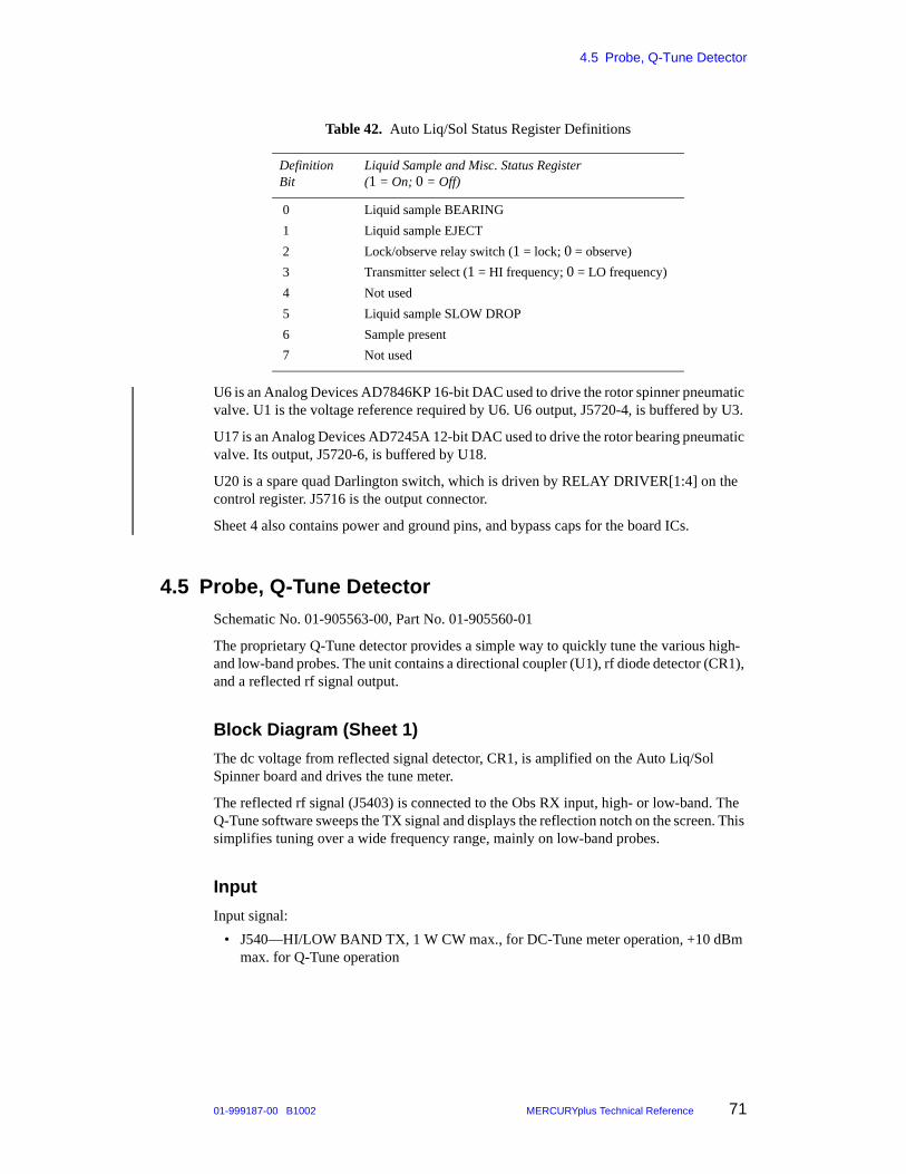
4.5 Probe, Q-Tune Detector
01-999187-00 B1002 MERCURYplus Technical Reference 71
U6 is an Analog Devices AD7846KP 16-bit DAC used to drive the rotor spinner pneumatic valve. U1 is the voltage reference required by U6. U6 output, J5720-4, is buffered by U3.
U17 is an Analog Devices AD7245A 12-bit DAC used to drive the rotor bearing pneumatic valve. Its output, J5720-6, is buffered by U18.
U20 is a spare quad Darlington switch, which is driven by RELAY DRIVER[1:4] on the control register. J5716 is the output connector.
Sheet 4 also contains power and ground pins, and bypass caps for the board ICs.
4.5 Probe, Q-Tune DetectorSchematic No. 01-905563-00, Part No. 01-905560-01
The proprietary Q-Tune detector provides a simple way to quickly tune the various high- and low-band probes. The unit contains a directional coupler (U1), rf diode detector (CR1), and a reflected rf signal output.
Block Diagram (Sheet 1)
The dc voltage from reflected signal detector, CR1, is amplified on the Auto Liq/Sol Spinner board and drives the tune meter.
The reflected rf signal (J5403) is connected to the Obs RX input, high- or low-band. The Q-Tune software sweeps the TX signal and displays the reflection notch on the screen. This simplifies tuning over a wide frequency range, mainly on low-band probes.
Input
Input signal:
• J540—HI/LOW BAND TX, 1 W CW max., for DC-Tune meter operation, +10 dBm max. for Q-Tune operation
Table 42. Auto Liq/Sol Status Register Definitions
DefinitionBit
Liquid Sample and Misc. Status Register(1 = On; 0 = Off)
0 Liquid sample BEARING
1 Liquid sample EJECT
2 Lock/observe relay switch (1 = lock; 0 = observe)
3 Transmitter select (1 = HI frequency; 0 = LO frequency)
4 Not used
5 Liquid sample SLOW DROP
6 Sample present
7 Not used

Chapter 4. Magnet Interface Box (MIB)
72 MERCURYplus Technical Reference 01-999187-00 B1002
Output
Output signals:
• E-3,4—DC voltage of reflected signal, 1 Mohm load, typically 2 V to 0.8 V, 100 to 400 MHz at 1 W CW, J5402 open.
• J5402—Probe in/out, probe tuned for minimum reflection signal.
• J5403—Reflected rf signal out, down by 35 dB typical from TX signal at full reflection (J5402 open). Down by 70 dB typical from TX signal with true 50-ohm load at J5402.
4.6 Automated Deuterium Gradient Shimming RelayPart No. 01-907219-00
The Automated Deuterium Gradient Shimming module switches the low-band observe signal to the 2H coil in the probe. This allows automated acquisition of a deuterium spectrum for gradient-based auto-shimming. The relay is located in the Magnet Interface box.

01-999187-00 B1002 MERCURYplus Technical Reference 73
Chapter 5. Power Supply
Sections in this chapter:
• 5.1 “System Power Supply” this page
• 5.2 “High-Band, High-Power RF Amplifier – 200-, 300-, 400-MHz Systems” page 75
• 5.3 “Low-Band, High-Power RF Amplifier – 200-, 300-, 400-MHz Systems” page 76
• 5.4 “High-Band, Low-Power RF Amplifier – 200-, 300-MHz Systems” page 77
• 5.5 “Low-Band, Low-Power RF Amplifier – 200-, 300-MHz Systems” page 78
• 5.6 “Dual Channel RF Amplifier – 300-, 400-MHz Systems” page 79
The MERCURYplus power supply is installed in the bottom rack position in the rear of the cabinet. The power supply operates from 110 volts ac and requires a transformer when used in locations with other voltages. The power supply weighs over 65 pounds, and care should be used when removing the supply from the cabinet.
The power supply contains two rf power amplifiers. Four different types of rf power amplifier modules are used, depending on whether the system configuration uses the 5-Nuclei Reference Generator board or the High/Low-Band Reference Generator board.
• 200, 300, 400 broadband systems with High/Low-Band Reference Generator board:
High-band, high-power rf amplifier, 75 W
Low-band, high-power rf amplifier, 125 W
• 200, 300 4-nuclei systems with 5-Nuclei Reference Generator board
High-band, low-power rf amplifier, 35 W
Low-band, low-power rf amplifier, 35 W
5.1 System Power SupplySchematic No. 01-901394-00, Part No. 01-901381-01
Figure 6. System Power Supply

Chapter 5. Power Supply
74 MERCURYplus Technical Reference 01-999187-00 B1002
The system power supply (shown in Figure 6) contains six linear power supply units and one high-band and one low-band rf power amplifier module. The power supply powers the rf amplifiers and the rf cardcage. The digital cardcage has a separate power supply mounted behind the digital cardcage, which is accessed by removing the cabinet side panel.
Two thermo switches are used to protect the supply from overheating in case of fan failure. The S201 thermoswitch triggers the system alarm at +65°C. The S200 thermoswitch resets circuit breaker CB201 at +82°C shutting off the complete system.
The PS202 supply must be set to minimum output voltages of +10.5 to +11 V and –10.5 to –11 V, and the PS201 supply must be set to +28 V. All other supplies are factory preset. Table 43 details the input signals for the power supply.
Table 44 shows power supply output signals.
Table 43. Power Supply Input Signals
Input signals Description
AC power 115 V ±10%, 50–60 Hz, 800 VA (optional units not included)
P8-4 High-band rf amp blanking
0 V or open = blanked
+5 V = unblanked
P8-7 Low-band rf amp blanking
0 V or open = blanked
+5 V = unblanked
J204 High-band rf amp input
188-301 MHz (35 W), 0 dBm max
188-401 MHz (75 W), 0 dBm max
J208 Low-band rf amp input
20–125 MHz (35 W), 0 dBm max
20–162 MHz (125 W), 0 dBm max
Table 44. Power Supply Output Specifications
Connector Pin Voltage Maxload Comments
P200 1 +28 V, ±3% 10 A High-band rf amplifier module Low-band rf amplifier moduleP201 1 +28 V, ±3% 10 A
P3 2 +10.5 to +11 V 2 A Shim/DAC driverShim/DAC driverP3 4 –10.5 to –11 V 2 A
P3 3 ±11 V return Shim/DAC driver
P2 3 –5 V, ± 3% 3 A RF backplane
P2 1 +5 V, ± 3% 6 A RF backplane
P1 1 +12 V, ± 3% 2.5 A RF backplane
P1 3 +24 V, ± 3% 3.6 A RF backplane
P1 5 –24 V, ± 3% 1.2 A RF backplane
P8 5 +28 V — RF amplifier thermoswitch
P8 6 +28 V — RF amplifier thermoswitch

5.2 High-Band, High-Power RF Amplifier – 200-, 300-, 400-MHz Systems
01-999187-00 B1002 MERCURYplus Technical Reference 75
5.2 High-Band, High-Power RF Amplifier – 200-, 300-, 400-MHz Systems
Part No. 00-993934-00
When a broadband system is specified, the high-band, high-power rf amplifier is installed in the power supply and the spectrometer is equipped with the High/Low-Band Reference Generator board. The solid state air-cooled rf amplifier module covers the frequency spectrum of 188 to 401 MHz with a peak power of 75 W and is equipped with an integrated heat sink.
Table 45 lists specifications for the amplifier.
Table 45. High-Band, High-Power Amplifier Specifications
Specification Tolerance
Frequency range 188 to 401 MHz, minimum
Output power 75 W min., pulsed, 15 W, CW max.
Maximum power, compressed 0% to 100% above minimum power, at 0 dBm input power
Power gain 49 dB min (0 dBm input power for 75 W output power)
Linearity Variation from linear, ±1.0 dB, typicalPower level, 0 to 75 WFrequency range, 188 to 401 MHz
Gain flatness versus frequency 0 dB to 4 dB max., measured at –15 dBm input power
Pulse width 1 ms max.
Duty cycle 10% max.
Signal rise and fall time 0.3 µs, max.
Amplitude droop, 75 W, 1 ms 3% typical, 5% max.
Blanking speed 2 µs, max.
Blanking ON/OFF ratio 60 dB/188 MHz, 50 dB/401 MHz
Output noise (blanked) 20 dB over thermal, max.
Noise figure 10 dB typical
Protection Temperature sensor switch opens at over temperature and also removes the +28 V from the amp. Input overdrive +10 dBm max.
Power requirements +28 V, 6 A peak
Cooling Forced air, 50 CFM min.

Chapter 5. Power Supply
76 MERCURYplus Technical Reference 01-999187-00 B1002
5.3 Low-Band, High-Power RF Amplifier – 200-, 300-, 400-MHz Systems
Part No. 00-993935-00
When a broadband system is specified, the solid state air-cooled rf amplifier module is installed in the spectrometer. The amplifier covers the frequency spectrum of 20- to 162-MHz with a peak power of 125 W and is equipped with an integral heat sink,
Table 46 lists specifications for the amplifier.
Table 46. Low-Band, High-Power Amplifier Specifications
Specification Tolerance
Frequency range 20 to 162 MHz, minimum
Output power 125 W min., pulsed, 25 W, CW max.
Maximum power, compressed ≥150 W at +1 to +2 dBm input power
Power gain 51 dB min. (0 dBm input power for 125 W output power)
Linearity Variation from linear, ±1.0 dB, typicalPower level, 0 to 125 WFrequency range, 20 to 162 MHz
Gain flatness versus frequency 0 dB to +4 dB max, measured at –15 dBm input power
Pulse width 1 ms max.
Duty cycle 10% max.
Amplitude rise and fall time 0.3 µs, max.
Amplitude droop, 125 W, 1 ms 3% typical, 5% max.
Blanking speed 2 µs, max.
Blanking ON/OFF ratio 70 dB/20 MHz, 60 dB/162 MHz
Output noise (blanked) 20 dB over thermal, max.
Noise figure 10 dB typical
Protection Temperature sensor switch opens at over- temperature and also removes the +28 V from the amplifier. Input overdrive +10 dBm max.
Power requirements +28 V, 10A peak
Cooling Forced air, 50 CFM min.

5.4 High-Band, Low-Power RF Amplifier – 200-, 300-MHz Systems
01-999187-00 B1002 MERCURYplus Technical Reference 77
5.4 High-Band, Low-Power RF Amplifier – 200-, 300-MHz Systems
Part No. 00-993936-00
This solid-state air-cooled rf amplifier module covers the frequency spectrum of 185 to 301 MHz with a peak power of 35 W and is equipped with an integral heat sink. This amplifier is used with the 4-nucleus rf system.
Table 47 lists specification for the amplifier.
Table 47. High-Band, Low-Power Amplifier Specifications
Specification Tolerance
Frequency range 185 to 301 MHz, minimum
Pulse power (min) into 50 ohms 35 W (0 dBm input power)
Maximum power, compressed 50% to 100% above minimum power, at 0 dBm input power
CW power (max) into 50 ohms 5 W
Power gain 45.5 dB min.
Linearity Variation from linear, ±1.0 dB, typicalPower level, 0 to 35 WFrequency range, 185 to 301 MHz
Input/output impedance 50 ohms
Input VSWR Less than 2:1 typical
Load VSWR tolerance Infinite
Pulse width 1 ms
Duty cycle Up to 10%
Amplitude rise and fall time 3 µs, max.
Amplitude droop, 1 ms 3% typical, 5% max.
Noise figure 8 dB typical
Output noise (blanked) Less than 20 dB over thermal
Blanking speed Less than 2 µs on/off, TTL signal
Blanking input impedance HCT type device, 10 kohm to ground
Blanking level Input open or grounded = blanked
Input +5 V = unblanked
Protection Temperature sensor switch opens at over temperature and also removes the +28 V from the amplifier. Input overdrive +10 dBm max.

Chapter 5. Power Supply
78 MERCURYplus Technical Reference 01-999187-00 B1002
5.5 Low-Band, Low-Power RF Amplifier – 200-, 300-MHz Systems
Part No. 01-902429-00
The low-band solid-state air-cooled rf amplifier module covers the frequency spectrum of 20 to 125 MHz with a peak power of 35 W and is equipped with an integral heat sink. This amplifier is used with the 4-nucleus rf system.
Table 48 lists specifications for the amplifier.
Table 48. Low-Band RF Low-Power Amplifier Specification
Specifications Tolerance
Frequency range 20 to 125 MHz, minimum
Pulse power (min) into 50 ohms 35 W (0 dBm input power)
Maximum power, compressed 50% to 100% above minimum power, at 0 dBm input power
CW power (max) into 50 ohm 5 W
Power gain 45.5 dB min
Linearity Variation from linear, ±1.0 dB, typicalPower level, 0 to 35 WFrequency range, 20 to 125 MHz
Input/output impedance 50 ohms
Input VSWR Less than 2:1 typical
Load VSWR tolerance Infinite
Pulse width 1 ms
Duty cycle Up to 10%
Amplitude rise and fall time 3 µs, max
Amplitude droop, 1 ms 3% typical, 5% max.
Noise figure 8 dB typical
Output noise (blanked) Less than 20 dB over thermal
Blanking speed Less than 2 µs on/off, TTL signal
Blanking input impedance HCT type device, 10k ohm to ground
Blanking level Input open or grounded = blankedInput +5V = unblanked
Thermal switch trip level +70°C
Protection Temperature sensor switch opens at over temperature and also removes the +28 V from the amplifier input overdrive +10 dBm max.

5.6 Dual Channel RF Amplifier – 300-, 400-MHz Systems
01-999187-00 B1002 MERCURYplus Technical Reference 79
5.6 Dual Channel RF Amplifier – 300-, 400-MHz Systems
Part No. 00-993200-00
This solid-state air-cooled rf amplifier module consists of two modules, which continuously cover the 6- to 500-MHz frequency spectrum with pulsed power outputs in the 50 to 300 W range. Both channels operate at the same time. This amplifier is used with the CP/MAS accessory.
Table 49 lists specifications for the amplifier.
Table 49. Dual Channel RF Amplifier Specifications
Units Channel B Channel A
Frequency Range MHz 6 - 19.9 20 - 220 201 - 221 200 -500
Min. Pulse Pwr into 50 ohm W 300 300 150 100
Min. CW Pwr into 50 ohm W 30 30 30 15
Linearity:
Variation From Linear dB 62 62 62 53
Power Level (min.) W 0 - 250 0 - 250 0 - 150 0 - 40
Frequency Range MHz 6 - 19.9 20 - 220 221 - 245 200 - 500
Gain:
Maximum dB 62 62 62 58
Minimum dB 56 56 56 52
Frequency Range MHz 6 - 19.9 20 - 220 221 - 245 200 - 500
Input/Output Impedance ohms 50 50 50 50
Input VSWR <2:1 <2:1 <2:1 <2:1
Maximum Amplitude
Rise/Fall Time ns 500 175 175 150
Frequency Range MHz 6 - 29.9 30 - 200 201 - 245 200 - 500
Simultaneous Operation Mode
Maximum Pulse Width ms 20 20 20 250
Maximum Duty Cycle % 10 10 10 10
Minimum Power W 150 300 150 100
Amplitude Droop
Power Out W 200 200 100 100
Pulse Width=10 ms (max) % 5 5 5 <5
(typical) % <3.5 <3.5 <3.5 ---
Power Out W 25
Pulse Width=250 ms (max) % <4
(typical) % 2.5
Typical Logic Blanking Delay
On (maximum) µs 1 1 1 1

Chapter 5. Power Supply
80 MERCURYplus Technical Reference 01-999187-00 B1002
Off (maximum) µs 1 1 1 1
Phase Change Over Linear Power Output Range
(maximum) degrees 20 20 20 20
(typical) <10 <10 <10 <10
Phase Error Over 10 ms pulse
(maximum) degrees 6 6 6 6
(typical) <4 <4 <4 <4
Noise Figure (maximum) dB 10 10 10 14
(typical) <8 <8 <8 <9
Output Noise (blanked)
Overthermal (maximum) dB 20 254 25 20
(typical) <20 <20 <20 <20
Units Channel B Channel A

01-999187-00 B1002 MERCURYplus Technical Reference 81
Chapter 6. Options
Sections in this chapter:
• 6.1 “Pulsed Field Gradient (PFG) Amplifier” page 82
• 6.2 “PFG Interface Board” page 87
• 6.3 “CP/MAS Accessory” page 90
• 6.4 “Variable Temperature (VT) Unit” page 91
• 6.5 “Automated Sample Management” page 93
Options for the MERCURYplus NMR console are the pulsed field gradient (PFG) Performa I and Performa II accessories, PFG Interface board, CP/MAS accessory, the variable temperature (VT) unit, and Automated Sample management. The Performa I and VT units are installed from the front of the cabinet and all controls and indicators are accessible from the front (see Figure 7). The front cabinet door can be removed when installing these accessories. The Performa II and CP/MAS accessories are installed in separate housings that sit on top the MERCURYplus cabinet. Other options include a sample changer and automated 2H gradient shimming.
Figure 7. Console Options
VT Unit
PFG amplifier
Chapter 6. Options
82 MERCURYplus Technical Reference 01-999187-00 B1002
6.1 Pulsed Field Gradient (PFG) AmplifierTwo options are available for PFG:
• “Performa I PFG” page 82
• “Performa II PFG” page 85
Performa I PFG
Part No. 01-901829-02
The Performa I (L600) PFG amplifier is a high-precision pulsed constant-current power source specifically designed to drive gradient magnetic field coils in NMR systems. The unit includes a digital interface via the AP (analog port) bus to the main NMR system AP bus and provides a single constant-current analog output to the gradient coil.
When the PFG amplifier is installed in the system, the AP bus terminators UR1, UR2, and UR3, located near the 50-pin AP bus connector J7 on the rf backplane, need to be removed. The L600 has internal AP bus terminators that must be installed properly. When replacing the L600, compare the replacement unit internal terminators to the original unit and change, if necessary.
When the PFG option is specified, in addition to the PFG amplifier, a PFG upper barrel, and PFG probe are required for the magnet.
Features and Specifications
Performa I features include:
• Wideband (15 kHz) response.
• Extremely low noise levels, typically below 5 ppm RMS of full scale.
• Extreme flatness; pulse tops and bottoms settle to within 100 ppm of final values within 300 microseconds.
• Low temperature-induced drifts, typically below 25 ppm per degree C.
• True transconductance amplifier topology, which provides high-impedance magnet drive, even beyond the system bandwidth. This feature greatly reduces load microphonic effects and makes control loop dynamics totally independent of load impedance.
• Protection and supervision circuits are included to protect both the L600 and the load from damage.

6.1 Pulsed Field Gradient (PFG) Amplifier
01-999187-00 B1002 MERCURYplus Technical Reference 83
The Performa I accepts digital data inputs and provides a pulsed constant-current coil drive. Table 50 lists the specifications for a basic PFG configuration.
Table 51 shows AP chip output I/O register information.
The AP chip register selects are set to 16-bit output mode.
Table 52 shows constant-current output specifications.
Table 50. Basic PFG Specifications
Description Specification
Line power configuration 110 Vac, 50 W max., 150 W peak during pulse
Line fuse 2 A
AC line code 110 V type
Dip switch S1 setting S1-8 OFFS1-7 ON
AP chip Part No. 00-992288-01
Front panel color Black
Table 51. AP Chip Output I/O Register
Register Information
0 bit 0-7 = lower 8 data bits of DAC, bit 0 is LSB
1 bit 0-3 = upper 4 data bits of DAC, bit 3 is MSB
2 bit 0 = power output stage enable bit (POWEREN+)
bit 1 = amplifier reset bit (AMPRESET+)
3 bit 0 = amplifier check bit from the amplifier (AMPOK+)
bit 2-7 = PFG configuration bits from the configuration switch
Table 52. PFG Constant-Current Output Specifications
Description Specification
Range ±3.0 A full-scale average
Output bipolar ±1.4 A max., steady-state (dc) or time-averaged over 5 seconds max.
RMS output 2.0 A max.
Pulse width Varies from 1 s max. at 3.0 A to infinite at 1.4 A
Load range 0 to 1.5 ohms DCR, 0 to 30 µH inductance
Output impedance 100 ohms min. at 15 kHz, increasing at lower frequencies as 1/F to at least 100 kohm below 15 Hz.
Rise time 25 µs typical rise time (10–90%)
Settling To ±100 ppm of step size within 300 µ for any load in specified load range.
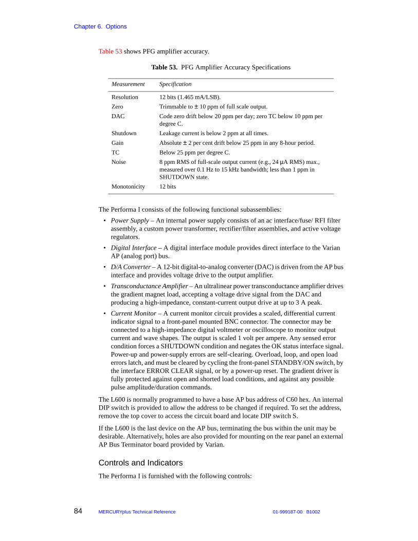
Chapter 6. Options
84 MERCURYplus Technical Reference 01-999187-00 B1002
Table 53 shows PFG amplifier accuracy.
The Performa I consists of the following functional subassemblies:
• Power Supply – An internal power supply consists of an ac interface/fuse/ RFI filter assembly, a custom power transformer, rectifier/filter assemblies, and active voltage regulators.
• Digital Interface – A digital interface module provides direct interface to the Varian AP (analog port) bus.
• D/A Converter – A 12-bit digital-to-analog converter (DAC) is driven from the AP bus interface and provides voltage drive to the output amplifier.
• Transconductance Amplifier – An ultralinear power transconductance amplifier drives the gradient magnet load, accepting a voltage drive signal from the DAC and producing a high-impedance, constant-current output drive at up to 3 A peak.
• Current Monitor – A current monitor circuit provides a scaled, differential current indicator signal to a front-panel mounted BNC connector. The connector may be connected to a high-impedance digital voltmeter or oscilloscope to monitor output current and wave shapes. The output is scaled 1 volt per ampere. Any sensed error condition forces a SHUTDOWN condition and negates the OK status interface signal. Power-up and power-supply errors are self-clearing. Overload, loop, and open load errors latch, and must be cleared by cycling the front-panel STANDBY/ON switch, by the interface ERROR CLEAR signal, or by a power-up reset. The gradient driver is fully protected against open and shorted load conditions, and against any possible pulse amplitude/duration commands.
The L600 is normally programmed to have a base AP bus address of C60 hex. An internal DIP switch is provided to allow the address to be changed if required. To set the address, remove the top cover to access the circuit board and locate DIP switch S.
If the L600 is the last device on the AP bus, terminating the bus within the unit may be desirable. Alternatively, holes are also provided for mounting on the rear panel an external AP Bus Terminator board provided by Varian.
Controls and Indicators
The Performa I is furnished with the following controls:
Table 53. PFG Amplifier Accuracy Specifications
Measurement Specification
Resolution 12 bits (1.465 mA/LSB).
Zero Trimmable to ± 10 ppm of full scale output.
DAC Code zero drift below 20 ppm per day; zero TC below 10 ppm per degree C.
Shutdown Leakage current is below 2 ppm at all times.
Gain Absolute ± 2 per cent drift below 25 ppm in any 8-hour period.
TC Below 25 ppm per degree C.
Noise 8 ppm RMS of full-scale output current (e.g., 24 µA RMS) max., measured over 0.1 Hz to 15 kHz bandwidth; less than 1 ppm in SHUTDOWN state.
Monotonicity 12 bits

6.1 Pulsed Field Gradient (PFG) Amplifier
01-999187-00 B1002 MERCURYplus Technical Reference 85
• Rear-panel power ON/OFF switch – Always turn ac power off when performing maintenance of any kind. For maximum stability, the ac power should be left ON at all times unless it is known that the PFG feature will not be required for extended periods.
• Front-panel ON/STANDBY switch – In the STANDBY position, the L600 output stages are inhibited, assuring low gradient coil current. When the switch is in the ON position and a remote enable is received from the console interface, the L600 enters active operating mode. If a latched error occurs, this switch may be cycled to STANDBY and then back ON to clear the error.
The front-panel rocker switch selects STANDBY and ON modes. If it is set to STANDBY, the amplifier output stage is “blanked” and the magnet current is forced to a very low level. In the ON position, the L600 enters the active ON state if the digital interface ON permissive signal is asserted.
Front-panel LED indicators include:
• POWER – Indicates ac power is on.
• ON – Indicates the Performa I is in operating mode (not standby).
• ACK – Flashes when the Performa I generates an AP bus ACKNOWLEDGE signal, indicating the completion of a bus transaction.
Error Reset
The Performa I can sense a number of error conditions, including an open load, an internal current error, and several internal failures. These errors “latch,” shutting down the unit. Cycling the STANDBY/ON switch resets any latched errors and resume normal operation, provided the error cause has been cleared. Latched errors can also be sensed and cleared from the system console.
Internal Adjustments
A single internal adjustment is provided, the ZERO trimpot. Since the zero-current output may drift with time (especially in the first few weeks of operation), users may wish to adjust the ZERO pot for zero current output. The preferred procedure is to connect a 100-ohm dummy load to the Performa I output and program the unit to turn ON with zero output current requested. Monitor the voltage across the 100-ohm load and adjust the zero trimpot for less than 1 mV drop across this load.
Performa II PFG
Part No. 00-992325-00
The Performa II (L700) is a single-axis, constant-current gradient magnet driver that provides a high-precision, pulsed constant-current drive to gradient field coils used in NMR and MRI applications.
The Performa II accepts digital data inputs, is AC powered, and includes all required power supplies, cooling, and local indicators.
Input Data Interface
Signal Levels
DATA signals are 2-wire, differential, RS-485 compatible. By convention, a signal called SIG consists of wires named SIG+ and SIG-, and the signal is considered active (true) if the SIG+ and SIG- line is electrically more positive than the SIG- line.

Chapter 6. Options
86 MERCURYplus Technical Reference 01-999187-00 B1002
FAILSAFE signals are 0/+ volt levels, active-high, 500-ohm nominal source drive impedance. Receivers of FAILSAFE signals must accept a zero volt signal or an open circuit as a failure, shutdown, or other safe-case logic level. Each signal has an associated active signal pin and a paired ground.
Interface Connector
Table 54 lists the pin assignments on the data interface connector.
Table 54. Performa II Data Interface
All data transfers are serial, 24-bit, with following strobe. The 20–bit current setpoint DAC value is preceded by four dummy bits, the sent MSB first in signed, 2’s complement format. An eddy current factor is sent as a 24–bit value, representing two 12–bit, unsigned values, which control the time constant and amplitude of each of the eddy exponential generators.
SDAT bits are accepted on the rising edge of CLK. Data is transferred into DACs by a positive STROBE pulse.
The ERROR RESET input, at its rising edge, clears any latched error conditions, providing that the error cause has been corrected.
The ENABLE input, when pulled up to +5, enables the current driver output stage. When open or at 0 volts, the output FETS are OFF and will demonstrate only leakage current levels, typically below 1 microampere. To avoid loop error after power up, when DAC contents may be unknown, users should load the current setpoint DAC with a zero-current request before asserting ENABLE.
The OK output is asserted to +5 volts when the L700 is powered up, enabled, in OPERATE mode, and has no error conditions present.
Controls and Indicators
The Performa II is furnished with the following controls:
• Rear-panel power ON/OFF switch – Always turn ac power off when performing maintenance of any kind. For maximum stability, the ac power should be left ON at all times unless it is known that the PFG feature will not be required for extended periods.
• Front-panel STANDBY/OPERATE switch – In the STANDBY position, the L700 output stage is disabled, but internal supplies and control circuits remain powered. When the switch is in the ON position and a remote enable is received from the console interface, the L700 enters active operating mode.
Name I/O +Pin –Pin Type Function
A0 Input 1 2 Data Register Select, LS bit
A1 Input 3 4 Data Register Select, LS bit
A2 Input 5 6 Data Register Select, MS bit
SDAT Input 7 8 Data Serial Data
CLK Input 9 10 Data Serial Data Clock
STB Input 11 12 Data Serial Data Storage
RST Input 15 16 Data Error Reset
ENABLE Input 17 18 FLSAF Power Stage Enable (pin 18 is GND)
OK Output 19 20 FLSAF OPERATING Indicator (pin 20 is GND)
Pin 13, 14, 25 grounds

6.2 PFG Interface Board
01-999187-00 B1002 MERCURYplus Technical Reference 87
• RESET push button - If a latched error occurs in OPERATE mode, the momentary RESET button can be pressed to clear the error.
Front-panel LED indicators include:
• POWER – Indicates ac power is available and on.
• OPERATE – Indicates the Performa II is in operating mode (not standby or shutdown).
• DATA – Indicates data transfer active.
• ERROR – Indicates power supply error.
• HITEMP – Indicates high temperature shutdown.
• WARMUP – Indicates warm-up or internal oven failure.
• LOAD – Indicates open load or blown load fuse.
Table 55 lists the Performa II constant-current output specifications.
Table 55. PFG Constant-Current Output Specifications
6.2 PFG Interface BoardSchematic No. 87-195857-00, Part No. 00-992542-00
The PFG Interface board provides the digital signals required for the control of the PFG Performa II (Highland L700) amplifier. The Highland amplifier contains a number of DACs that require serial data input.
The PFG interface can be supplied with or without a waveform generator. The configuration determines how the Highland current setpoint DAC is controlled. The setpoint DAC is responsible for the amplitude of the current pulse generated by the L700. When supplied with a waveform generator, the waveform generator's parallel output is transformed into serial data and then sent to the Highland Amplifier. When no waveform generator is present, the AP bus provides the information that the PFG interface converts into serial data and sends to the Highland amplifier. In either case, the four eddy current compensation DACs within the Highland are set by converting AP bus information to serial data. All of the DAC's in the Highland require the same timing on the digital interface, even though the current setpoint is an AD1862 and the eddy current DAC's are DAC7800's.
Block Diagram (Sheet 1)
The present design separates the sections that do the parallel-to-serial conversion for both configurations. Page 2 of the schematic contains the circuitry to interface to a waveform
Description Specification
Range ±10.0 A full-scale DAC range
Average Output bipolar
±4.0 A max., steady-state (dc) or time-averaged over 1.25 seconds max.
RMS output 7.5 A max.
Pulse width Varies from 500 ms max. at 10.0 A to infinite at 4.0 A
Peak output ±10.0 A with eddy compensation off; with ECC enabled, peak current may hit 20 A for 1 ms, and 15 A for 60ms max.
Duty cycle Varies from 0.40 at 10 A to 1.00 at 4.0 A, averaged over 1.25 s maximum interval.

Chapter 6. Options
88 MERCURYplus Technical Reference 01-999187-00 B1002
generator; it also has all the gating/clock circuitry. Sheet 3 of the schematic shows the AP Bus Interface circuitry. The final page has the output multiplexer, line drivers, and power up circuitry.
Wavegen Circuit (Sheet 2)
In the wavegen configuration, there is a straight 24-bit conversion that employs three 8-bit shift registers, U1A, U1B, and U1C. The signal WG_STB(Wavegen Strobe) clocks 16 bits of parallel data into the ACT299 shift registers and clocks in the appropriate count into the LS592, U3B. A data stream of 24 bits is necessary to get a compatible interface for both types of DAC’s in the L700. The DAC7800, used in the eddy current compensation, is a dual 12-bit DAC requiring 24 bits of data; the AD1862 is a 20-bit DAC, though it is guaranteed monotonic to only 17 bits. As a result, the PFG interface sends 4 dummy bits, then 16 valid bits, and finally 4 more dummy bits to the L700. After the parallel data has been latched into the shift registers on the rising edge of WG_STB, the falling edge sets the function code for the ACT299 to shift right by clocking latch U4B. This falling edge also enables the clock circuitry.
All clocks are derived from U2C, a gated 10 MHz oscillator whose output phase is fixed with respect to its enable input. U3C and U4C are used to appropriately gate the output of U2C; they control the clocks used for the shifting by the parallel to serial converters, the clocks used by the counters checking how many bits have been sent, and the clocks used as part of the serial communication link between the Highland and this board. The oscillator is only pulsing when data is being sent to the Highland; this is done to limit the amount of noise in the system.
After counting to 24, 8-bit counter U3B puts out a pulse whose edge is used to trigger the strobe for the Highland DAC. Pulse generator U3A furnishes the reset pulse that resets both the counter and the latch U4B.
AP Bus (Sheet 3)
The AP Bus is interfaced primarily by the APB chip, U5F. Note that there are two possible hookups for the AP bus. Connector J1 is a standard dual row 50-pin connector that is normally associated with the AP bus cable. Connector P2 is a 96-pin DIN connector that is compatible with the backplane on the Imaging/3rd Channel systems; those backplanes contain a buffered AP bus. The PFG interface can also be inserted into the 160-220 mm Extender card (00-992318-00) that will be used on future systems with 220 mm deep card card cages. Only P2 or J1 should be plugged in at any one time for proper operation (it is also rather difficult to do so simultaneously with a normal console). Note also that when the PFG interface is not in a card cage, J4 can be used to provide a separate power input; when in a card cage, power is supplied over P2.
The circuitry for converting the AP bus information to serial is very similar to that of the Wavegen described above.
Data is sent in 3 bytes to register 1 of the AP chip. After each byte is sent, shift register U4E converts it into serial information. The STB1 signal from the AP chip is analogous to WG_STB. It is used to clock an AP_ACTIVE signal to the output of latch U5E, it clocks the data into the ACT 299 shift register, and it clocks the count of 8 into LS592 U3E. U5D counts to 3 and then enables gate U3D; the pulse generated by U3E passes through the gate and its edge is used to create the strobe for the Highland DACs. Pulse generator U5C is analogous to U3A in function, providing the reset to latch U5E, shift register U4E and counter U3E. Address information is sent to the lowest three bits of register 0 of the AP Chip. This information is sent in parallel fashion to the Highland.

6.2 PFG Interface Board
01-999187-00 B1002 MERCURYplus Technical Reference 89
Output (Sheet 4)
The data, clock and strobe pulses all arrive at multiplexer U2E. The multiplexer chooses between the signals from the wavegen and those from the AP bus circuitry according to the state of the WG_ACTIVE line. When true, that signal also forces the address lines to zero at U2F because the wavegen can only control the setpoint DAC and not the eddy current compensation DACs. The edge of the strobe triggers one shot U2G to create the strobe for the Highland DACs. All the signals except ENABLE and OK are sent through U1E and U1F, two differential line drivers.
ENABLE is sent to the Highland by a 74HC14; it is used to enable the power stage of the L700.
OK is sent by the Highland l&L700 to indicate that no errors exist; it is received by 74HC14 U1D.
AMP_RESET is a 60 ms pulse generated by U1G; this clears any fault lines within the Highland (if the fault no longer exists).
The output to the L700 is sent through 25-pin D shell, J3.
Diagnostics (Sheet 4)
There are three green LED indicators, DS1-3, for each of the three address lines. When lit, it indicates that the line is high. There is also a green LED on DS1 tied to one shot U1G to indicate whether a strobe has been sent to the Highland. Red LED, DS2, indicates the status of the Highland OK signal; if lit, then the Highland is either powered off or has a problem. Green LED, DS3, indicates whether the Highland is enabled or not; if lit, the L700 power stage is enabled. Testpoints are provided for the strobe, data, and clock signals to the Highland. There is also a testpoint, TP1, for APACK-. This board has also been designed in accordance with ICT (in circuit test) guidelines.
An 8-bit dip switch is located on AP chip register 3; this can be used in the future for configuration readback if implemented in software.
Initialization (Sheet 4)
The board has a power up reset circuit that initializes all counters and latches. It also sends a serial data stream of zeroes to the Highland setpoint DAC upon power up of the Interface board. It does so by activating the wavegen circuitry on sheet 2. Push-button switch SW3 provides the same function as the power up circuit. An AP reset will send a zero to the Highland setpoint DAC. A zero can be sent to any DAC by writing a 1 to AP register 0, bit 3.
Addresses
The PFG Interface resides at AP Address C.
Register selection is determined by dip switch SW2 as follows:
Register Position 1 Position 2
50-53 (X) ON ON
54-57 (Y) ON OFF
58-5B (Z) OFF ON

Chapter 6. Options
90 MERCURYplus Technical Reference 01-999187-00 B1002
Note that positions 3 and 4 of the switch are not connected. For most PFG applications, SW2 is set for 58-5B.
The 25-pin interface contains 3 address lines, A0-A2. Whenever the wavegen strobes information, these lines are set to 0, corresponding to the address of the Highland setpoint DAC. Otherwise, these lines will be driven by register 0 of the AP chip as follows:
AP DAC Loading Sequence
aa=address, dd=data, x=don’t care
Note that a zero can be sent to any DAC by writing a high to bit 3 of register 0.
Other I/O Signals
6.3 CP/MAS AccessoryThe CP/MAS accessory allows the spectrometer to perform cross polarization/magic angle spinning experiments. The accessory adds a 100-W high-band amplifier and a 300-W low-band amplifier (see 5.6 “Dual Channel RF Amplifier – 300-, 400-MHz Systems” page 79), as well as pneumatics for either manual or computer-controlled high-speed spinning. The pneumatics are fully described in the Pneumatics/Tachometer Box Installation Pub. No. 01-999179-00. CP/MAS probes are available in 5-mm or 7-mm. The XPOLAR1 sequence is the only one supplied with the MERCURYplus and the MERCURY-VX.
A2 A1 A0 Addressed
0 0 0 Current setpoint DAC
0 0 1 Eddy Comp #1
0 1 0 Eddy Comp #2
0 1 1 Eddy Comp #3
1 0 0 Eddy Comp #4
AC50 address the AP chip
BCxa load reg 0 with the appropriate DAC address
bit 0 = A0
bit 1 = A1
bit 2 = A2
9Cxd load reg 1 with 4 dummy bits and the most significant nibble for setpoint DAC; load valid byte (dd) if for eddy current compensation DAC’s
BCdd load reg 1 with next byte of data
BCdd load reg 1 with most significant byte, LSB = bit 0
Enable The power stage enable line for the amplifier is a static line that will be connected to AP register 2, bit 0. A high will enable the output stage of the amplifier.
Reset The error reset line will be connected to AP register 2, bit 1. A high on this line will generate a pulse that will clear any latched error conditions on the amplifier.
OK This line is an input from the amplifier that can be read on AP register 3, bit 0.

6.4 Variable Temperature (VT) Unit
01-999187-00 B1002 MERCURYplus Technical Reference 91
6.4 Variable Temperature (VT) UnitPart No. 01-904189-00
The VT unit (L900) enables precise computer control of sample temperatures from −150°C to +250°C (the NMR default is +200°C). The L900 is a closed-loop temperature controller for NMR sample temperature stabilization, via a chilled/reheated gas loop. The temperature is controlled by flowing gas, usually nitrogen, around the sample in the probe. The gas is heated or cooled as required.
The VT unit has user selectable input voltage. When adding a VT unit to an existing MERCURYplus system, verify that the unit is set for 100/120 volts and that the 2A slow-blow type 3AG fuse is installed.
There are two switches: power ON/OFF and Heater ON/OFF. The Heater ON/OFF is a standby switch. When OFF, the power to the heater is disabled, but internal supplies and control circuits remain powered.
Table 56 lists VT specifications.
Table 56. VT Specifications
Description Specification
Range –150 to +250° C (gas flow range 5 to 25 LPM)
Output power 80 W min. into a 20-ohm heater, 150 W min. into 4-ohm heater. 6 open collector outputs, outputs are diode-clamped to the +12 V unregulated supply
Sensor Copper/constantan thermocouple. RTD nominal resistance is 180 ohms
Heater 20 ohm (ea. liquid probes); 4 ohm (ea. solid probes)
Control Bidirectional 3-wire RS-232 port, 9600 baud, Constrained PID closed-loop temperature control
Accuracy ±0.1° C with constant carrier gas flow
Stability ±0.1° C after warm-up and over 24 hours
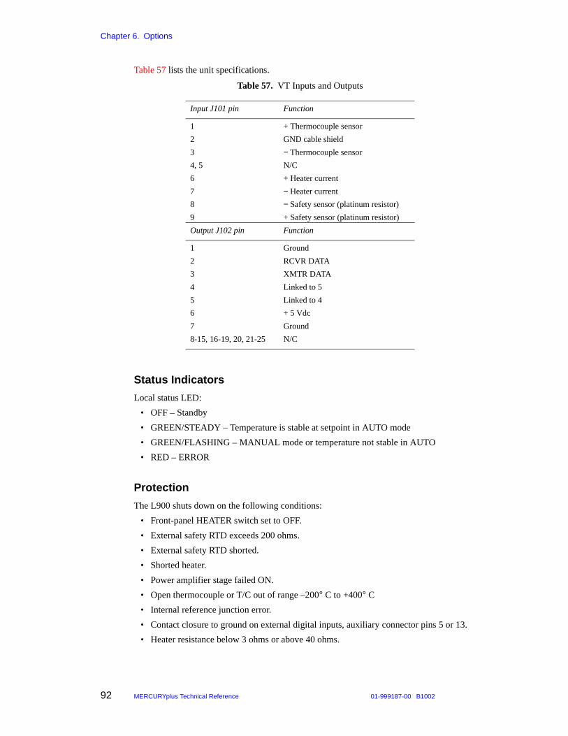
Chapter 6. Options
92 MERCURYplus Technical Reference 01-999187-00 B1002
Table 57 lists the unit specifications.
Status Indicators
Local status LED:
• OFF – Standby
• GREEN/STEADY – Temperature is stable at setpoint in AUTO mode
• GREEN/FLASHING – MANUAL mode or temperature not stable in AUTO
• RED – ERROR
Protection
The L900 shuts down on the following conditions:
• Front-panel HEATER switch set to OFF.
• External safety RTD exceeds 200 ohms.
• External safety RTD shorted.
• Shorted heater.
• Power amplifier stage failed ON.
• Open thermocouple or T/C out of range –200° C to +400° C• Internal reference junction error.
• Contact closure to ground on external digital inputs, auxiliary connector pins 5 or 13.
• Heater resistance below 3 ohms or above 40 ohms.
Table 57. VT Inputs and Outputs
Input J101 pin Function
1 + Thermocouple sensor
2 GND cable shield
3 − Thermocouple sensor
4, 5 N/C
6 + Heater current
7 − Heater current
8 − Safety sensor (platinum resistor)
9 + Safety sensor (platinum resistor)
Output J102 pin Function
1 Ground
2 RCVR DATA
3 XMTR DATA
4 Linked to 5
5 Linked to 4
6 + 5 Vdc
7 Ground
8-15, 16-19, 20, 21-25 N/C
6.5 Automated Sample Management
01-999187-00 B1002 MERCURYplus Technical Reference 93
6.5 Automated Sample Management The following sample management systems are available as options:
• An SMS autosampler with 50 or 100 sample rack.
• The 9-sample carousel autosampler.
• The versatile auto sample transport (VAST) sample management system.
• Nano Multi Sample (NMS) sample management system.
For technical and installation details, refer to the manual Sample Management Systems.

Chapter 6. Options
94 MERCURYplus Technical Reference 01-999187-00 B1002

01-999187-00 B1002 MERCURYplus Technical Reference 95
IndexIndex
Numerics16-bit Analog-to-Digital Conversion board, 231H hetero decoupler, 482H NMR lock signal, 562H probe preamp, 66
AAcquisition CPU board, 13Analog-to-Digital Conversion (ADC) board, 23Auto Liq/Sol Spinner board, 68Automated Deuterium Gradient Shimming Relay,
72axial DACs output, 61axial resistor matrixes, 62
Bbroadband lock receiver, 56broadband observe receiver, 46broadband preamplifier (medium power), 75broadband system, 76
CCDE (Common Desktop Environment), 12console left cardcage, 13CP/MAS accessory, 90cross polarization/magic angle spinning
experiments, 90CW 1H hetero decoupler, 48
DDeuterium Gradient Shimming relay, 72digital cardcage, 13
GGaAs FET preamps, 67gated 1H and 19F observe signals, 48gated 1H homo decoupler signal, 50gated L.O. and TX signals, 52
Hhigh/low-band reference generator, 39high-band observe transmitter, 48high-band preamplifier, 67high-band, high-power rf amplifier, 75high-band, low-power amplifier, 77Homonuclear Decoupler board, 50host computer, 11
Iindirect detection feature, 46
JJunction board, 30
LL600, 82L700, 85lock ADC channel, 24lock level indicator, 56lock preamplifier, 66lock receiver detector reference signal, 52, 53lock transmitter, 52, 53low-band broadband preamplifier, 66low-band rf low-power amplifier, 78low-band transmitter, 44low-band, high-power amplifier, 76
MMagnet and Magnet Interface Box, 9Mercury Interface box, 65MIB, 65
NNMR console, 9, 29NMS, 93notational conventions, 9
OOutput board, 14overheating protection, 74
PPerforma I, 82Performa II, 85PFG amplifier, 82PFG Interface board, 87pneumatics, 65Probe, Q-Tune Detector, 71
QQ-Tune detector, 71quadrature detection, 23quadrature lock signal channels, 56quadrature observe signals, 46
Rradial shim drive circuits, 62reference generator, 39reference rf signals, 39rf amplifier, 76rf cardcage, 29
Ssample management system, 93shim DAC/driver, 58STM board, 14sum-to-memory board, 14Sun workstation, 11
Index
96 MERCURYplus Technical Reference 01-999187-00 B1002
system alarm (beeper), 33system power supply, 74
VVME bus interface, 14-Bit ADC, 23VNMR data acquisition, 12VxWorks, 13
ZZ0 lock loop channel, 56