max14690 wearable cargemanagement soltion · general description the max14690 is a...
TRANSCRIPT

General DescriptionThe MAX14690 is a battery-charge-management solution ideal for low-power wearable applications. The device includes a linear battery charger with a smart power selector and several power-optimized peripherals. The MAX14690 features two ultra-low-power buck regulators with a typical quiescent current of 900nA. In addition, three ultra-low power low-dropout (LDO) linear regulators, with a typical quiescent current of 600nA are included. In total, the MAX14690 can provide up to five regulated voltages, each with an ultra-low quiescent current, critical to battery life for the unique power profile in 24/7 operation devices, such as those in the wearable market.The battery charger features a smart power selector that allows operation on a dead battery when connected to a power source. To avoid overloading a power adapter, the input current to the smart power selector is limited based on an I2C register setting. If the charger power source is unable to supply the entire system load, the smart power control circuit supplements the system load with current from the battery.The two synchronous, high-efficiency step-down buck regulators feature a fixed-frequency PWM mode for tighter regulation and a burst mode for increased efficiency during light-load operation. The output voltage of these regulators can be programmed through I2C with the default preconfigured. The three configurable LDOs each have a dedicated input pin. Each LDO regulator output voltage can be programmed through I2C with the default preconfigured. The linear regulators can also be configured to operate as power switches that may be used to disconnect the quiescent load of the system peripherals. The MAX14690 features a programmable power controller that allows the device to be configured for applications that require the device be in a true-off, or always-on, state. The controller also provides a delayed reset signal and voltage sequencing. The MAX14690 is available in a 36-bump, 0.4mm pitch, 2.72mm x 2.47mm wafer-level package (WLP).
Benefits and Features Extend System Use Time Between Battery Charging
• Dual Ultra-Low-IQ 200mA Buck Regulators - Output Programmable from 0.8V to 1.8V and 1.5V to 3.3V
- 0.9μA (typ) Quiescent Current - Automatic Burst or Forced-PWM Modes
• Three Ultra-Low-IQ 100mA LDOs - Output Programmable from 0.8V to 3.6V - 0.6μA (typ) Quiescent Current - 2.7V to 5.5V Input with Dedicated Pin
Easy-to-Implement Li+ Battery Charging• Smart Power Selector• 28V/-5.5V Tolerant Input• Thermistor Monitor
Minimize Solution Footprint Through High Integration• Provides Five Regulated Voltage Rails• Switch Mode Option on Each LDO
Optimize System Control• Monitors Pushbutton for Ultra-Low Power Mode• Power-On Reset Delay and Voltage Sequencing• On-Chip Voltage Monitor Multiplexer
Applications Wearable Electronics Fitness Monitors Portable Medical Devices
19-7480; Rev 11; 5/16
Ordering Information appears at end of data sheet.
MAX14690 Wearable Charge-Management Solution
MAX14690
SYS
LINEARLi+ BATTERY CHARGER
WITH POWER SELECTOR
28V INPUTPROTECTION
POWERSEQUENCER BUCK 1
MONITOR BUCK 2
CONTROL
LDO/SWITCH 1
LDO/SWITCH 2
LDO/SWITCH 3
POWER
DATA
Block Diagram
MAX14690 Wearable Charge-Management Solution
www.maximintegrated.com Maxim Integrated 2
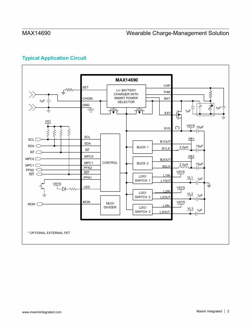
Typical Application Circuit
Li+ BATTERYCHARGER WITHSMART POWER
SELECTORBAT
THM
CAP
SYS
CHGIN
SET
MUX/DIVIDER
SCL
SDA
INT
MPC0
CONTROL
GND
MAX14690
VSYSVIO
L3OUT
L3IN
MPC1 BUCK 2B2LX
BUCK 1
B1OUT
B1LX
LDO/SWITCH 1
L1IN
L1OUT
L2IN
1µF
1µF1µF
10µF
10µF
10µF
1µF
2.2µH
SCL
SDA
INT
MPC0
MPC1
LDO/SWITCH 2
LDO/SWITCH 3
B2OUT
L2OUT
VSYS
VSYS
VSYS
PFN2
PFN1
PFN2
MON
1µF
1µF
2.2µH
LED
EXT
MON
* OPTIONAL EXTERNAL FET
VL3
VL2
VB2
VB1
VL1
VSYS
RST RST
(*)

(Voltages referenced to GND.)SDA, SCL, THM, RST, SYS, PFN1, PFN2,
MPC0, MPC1, INT, MON, BAT LED, L1IN, L2IN, L3IN .............................................. -0.3V to +6.0V
B1LX, B2LX, B1OUT, B2OUT, EXT ...... -0.3V to (VSYS + 0.3V)L1OUT ................................................... -0.3V to (VL1IN + 0.3V)L2OUT ................................................... -0.3V to (VL2IN + 0.3V)L3OUT ................................................... -0.3V to (VL3IN + 0.3V)CHGIN .................................................................... -6V to +30VCAP .................................... -0.3V to min (VCHGIN + 0.3V, +6V)SET .......................................................... -0.3V to VBAT + 0.3V
Continuous Current into CHGIN, BAT, SYS ................±1000mAContinuous Current into any other terminal ..................±100mAContinuous Power Dissipation (multilayer board at +70°C): 6 x 6 Array 36-Bump 2.72mm x 2.47mm
0.4mm Pitch WLP (derate 21.70mW/°C) .......................1.74WOperating Temperature Range ........................... -40°C to +85°CJunction Temperature ......................................................+150°CStorage Temperature Range ............................ -65°C to +150°CLead Temperature Soldering (10s) ..................................+300°CSoldering Temperature (reflow) .......................................+260°C
WLP Junction-to-Ambient Thermal Resistance (θJA) ..........46°C/W
(Note 1)
(VCHGIN = 5.0V, VBAT = 3.7V, TA = -40°C to +85°C, all registers in their default state, unless otherwise noted. Typical values are at TA = +25°C.) (Note 2)
PARAMETER SYMBOL CONDITIONS MIN TYP MAX UNITS
GLOBAL SUPPLY CURRENT (L_IN Connected to SYS)
Charger Input Current ICHG
All functions disabled 0.26
mAPower on, VCHGIN = 5VSYS switch closed, buck regulators in burst mode, LDO1 enabled, ISYS = 0A, IB_OUT = 0A, IL_OUT = 0A
2
BAT Input Current IBAT
Power off, VCHGIN = 0V,SYS switch open 0.95
µA
Power on, VCHGIN = 0VSYS switch closed, 2x buck regulators in Burst mode, LDOs disabled. ISYS = 0A, IB_OUT = 0A
3
Power on, VCHGIN = 0VSYS switch closed, 2x buck regulators in Burst mode, LDO1 enabled, ISYS = 0A, IB_OUT = 0A, IL_OUT = 0A
3.5
Power on, VCHGIN = 0VSYS switch closed, 2x buck regulators in burst mode, 3x LDOs enabled, ISYS = 0A, IB_OUT = 0A, IL_OUT =0A
4.6
MAX14690 Wearable Charge-Management Solution
www.maximintegrated.com Maxim Integrated 3
Note 1: Package thermal resistances were obtained using the method described in JEDEC specification JESD51-7, using a four-layer board. For detailed information on package thermal considerations, refer to www.maximintegrated.com/thermal-tutorial.
Absolute Maximum Ratings
Stresses beyond those listed under “Absolute Maximum Ratings” may cause permanent damage to the device. These are stress ratings only, and functional operation of the device at these or any other conditions beyond those indicated in the operational sections of the specifications is not implied. Exposure to absolute maximum rating conditions for extended periods may affect device reliability.
Package Thermal Characteristics
Electrical Characteristics

(VCHGIN = 5.0V, VBAT = 3.7V, TA = -40°C to +85°C, all registers in their default state, unless otherwise noted. Typical values are at TA = +25°C.) (Note 2)
PARAMETER SYMBOL CONDITIONS MIN TYP MAX UNITS
BUCK REGULATOR 1(VSYS = +3.7V, Burst mode operation, L = 2.2µH, C = 10µF, VB1OUT = 1.2V)
Input Voltage VIN_BUCK1 Input voltage = VSYS 2.7 5.5 V
Output Voltage VOUT_BUCK1 25mV step resolution (Note 3) 0.8 1.8 V
Quiescent Supply CurrentIQ_BUCK1 Burst mode, IOUT = 0mA (Note 4) 0.915 2 µA
IPWM1_BUCK1FPWM mode, L = 4.7µH (ESR = 0.6Ω, 2MHz RAC = 2.13Ω), IOUT = 0mA 2.5 3.5 mA
Output Accuracy ACCBUCK1IOUT = 1mA (VOUT_BUCK1 > 1V, C > 50µF) -2.6 +2.9 %
Load Regulation VERR_BUCK1From IOUT = 0 to 200mA (VB1OUT = 1.2V average voltage) -3 -1 %
Peak-to-Peak Ripple in Burst Mode VPPRIPPLE1
IOUT = 10mA, C = 20µF 25mV
IOUT = 10mA, C = 10µF 43
Maximum Operative Output Current IOUT_BUCK1 200 mA
B1OUT Pulldown Current ILEAK_B1OUTVOUT = VSYS 200 350 µA
VREG < VOUT < VREG + 0.1V 10 100 nA
pMOS On-Resistance RONP_BUCK1 0.22 0.4
nMOS On-Resistance RONN_BUCK1 0.18 0.3
Oscillator Frequency fBUCK1 FPWM mode 1.78 2 2.24 MHz
Maximum Duty Cycle DMAX_BUCK1 100 %
Short-Circuit Current Limit ISHRT_BUCK1 1.1 1.3 1.62 A
BLX Leakage Current IBLX_BUCK1 1 µA
Active Discharge Current ID_BUCK1 VB1OUT = 1.2V 8 18 36 mA
Full Turn-On Time TON_BUCK1 Time from enable to full current capability 58 ms
Thermal-Shutdown Temperature TSHDN_BUCK1 150 °C
Thermal-Shutdown Temperature Hysteresis TSHDN_HYST_BUCK1 20 °C
MAX14690 Wearable Charge-Management Solution
www.maximintegrated.com Maxim Integrated 4
Electrical Characteristics (continued)

(VCHGIN = 5.0V, VBAT = 3.7V, TA = -40°C to +85°C, all registers in their default state, unless otherwise noted. Typical values are at TA = +25°C.) (Note 2)
PARAMETER SYMBOL CONDITIONS MIN TYP MAX UNITS
BUCK REGULATOR 2(VSYS = +3.7V, Burst mode operation, L = 2.2µH, C = 10µF, VB2OUT = 1.8V.)
Input Voltage VIN_BUCK2 Input voltage = VSYS 2.7 5.5 V
Output Voltage VOUT_BUCK2 50mV step resolution 1.5 3.3 V
Quiescent Supply Current (Note 4)
IQ_BUCK2 Burst mode, IOUT = 0mA (Note 4) 1 2 µA
IPWM1_BUCK2FPWM mode, L = 4.7µH (ESR = 0.6W, 2MHz RAC = 2.13W) IOUT = 0mA 2.4 3.5 mA
Output Accuracy ACCBUCK2IOUT = 1mA, VOUT_BUCK2 > 1.5V, C > 50µF, VSYS > VB2OUT + 150mV -2 +2.93 %
Load Regulation VERR_BUCK2From IOUT = 0 to 200mA, VB2OUT = 1.8V average voltage -3.1 -1 %
Peak-to-Peak Ripple In Burst Mode VPPRIPPLE2
IOUT = 10mA, C = 20µF 38mV
IOUT = 10mA, C = 10µF 54
Maximum Operative Output Current IOUT_BUCK2 200 mA
B2OUT Pulldown Current ILEAK_B2OUTVOUT = VSYS 5 10 µA
VREG < VOUT < VREG + 0.1V 10 nA
pMOS On-Resistance RONP_BUCK2 0.22 0.4 Ω
nMOS On-Resistance RONN_BUCK2 0.18 0.3 Ω
Oscillator Frequency fBUCK2 FPWM mode 1.78 2.00 2.24 MHz
Maximum Duty Cycle DMAX_BUCK2 100 %
Short-Circuit Current Limit ISHRT_BUCK2 1.4 1.8 2.2 A
BLX Leakage Current IBLX_BUCK2 1 µA
Active Discharge Current ID_BUCK2 VB2OUT = 1.8V 8 18 36 mA
Full Turn-On Time tON_BUCK2 Time from enable to full current capability 58 ms
Thermal-Shutdown Temperature TSHDN_BUCK2 150 °C
Thermal-Shutdown Temperature Hysteresis TSHDN_HYST_BUCK2 20 °C
MAX14690 Wearable Charge-Management Solution
www.maximintegrated.com Maxim Integrated 5
Electrical Characteristics (continued)

(VCHGIN = 5.0V, VBAT = 3.7V, TA = -40°C to +85°C, all registers in their default state, unless otherwise noted. Typical values are at TA = +25°C.) (Note 2)
PARAMETER SYMBOL CONDITIONS MIN TYP MAX UNITSLDOs(C = 1µF, unless otherwise noted. Typical values are at VL_IN = 3.7V, with IL_OUT = 10mA, VL_OUT = 3V.)
Input Voltage VIN_LDOLDO_Mode = 0 2.7 5.5 V
LDO_Mode = 1 1.8 5.5 V
Quiescent Supply CurrentIQ_LDO IL_OUT = 0mA 0.56 1.2 µA
IQ_LDO_ADIL_OUT = 0mA, VL_IN = 1.8V, LDO_ActDSC = 1, LDO_En = 00 40 µA
Maximum Output Current IL_OUT_MAX 100 mA
Output Voltage VL_OUT 0.8 3.6 V
Output Accuracy ACCLDOVL_IN = (VL_OUT + 0.5V) or higher, IL_OUT = 100µA 3 %
Dropout Voltage VDROP_LDOVL_IN = 3.3V, IL_OUT_ = 100mA, VL_OUT = 3.3V 100 mV
Line Regulation Error VLINEREG_LDO VL_IN = (VL_OUT + 0.5V) to 5.5V -0.09 0.09 %/V
Load Regulation Error VLOADREG_LDO IL_OUT = 100µA to 100mA 0.003 0.008 %/mA
Line Transient VLINETRAN_LDOVL_IN = 4V to 5V, 200ns rise time ±36 mV
VL_IN = 4V to 5V, 1µs rise time ±28 mV
Load Transient VLOADTRAN_LDOIL_OUT = 0mA to 10mA, 200ns rise time 145 mV
IL_OUT = 0mA to 100mA, 200ns rise time 290 mV
Active Discharge Current IPDL VL_IN = 3.7V 9 21 37 mA
Turn-On Time tON_LDO
IL_OUT = 0mA, time to 90% of final value 2.3 ms
VL_IN = 3V, switch mode, IL_OUT = 0mA, time to 90% of final value 0.45 ms
Short-Circuit Current Limit ISHRT_LDOVL_OUT = GND 385 mA
VL_OUT = GND, switch mode 375 mA
Switch Mode Resistance RON_LDOVL_IN = 2.7V, switch mode 0.58 0.9 Ω
VL_IN = 1.8V, switch mode 0.89 1.35 Ω
Thermal-Shutdown Temperature TSHDN_LDO 150 °C
Thermal-Shutdown Temperature Hysteresis TSHDN_HYST_LDO 16 °C
Output Noise OUTNOISE
10Hz to 100kHz, VL_IN = 5V, VL_OUT = 3.3V 110
µVRMS
10Hz to 100kHz, VL_IN = 5V, VL_OUT = 2.5V 95
10Hz to 100kHz, VL_IN = 5V, VL_OUT = 1.2V 60
10Hz to 100kHz, VL_IN = 5V, VL_OUT = 0.8V 60
MAX14690 Wearable Charge-Management Solution
www.maximintegrated.com Maxim Integrated 6
Electrical Characteristics (continued)

(VCHGIN = 5.0V, VBAT = 3.7V, TA = -40°C to +85°C, all registers in their default state, unless otherwise noted. Typical values are at TA = +25°C.) (Note 2)
PARAMETER SYMBOL CONDITIONS MIN TYP MAX UNITS
CHGIN TO SYS PATH(VCHGIN = 5.0V, VSYS = VSYS_REG.) (Note 2)
Allowed CHGIN Input Voltage Range VCHGIN_RNG -5.5 28 V
Allowed BAT Voltage Range VBAT_RNG 0 5.5 V
VCHGIN Detect Threshold VCHGIN_DETRising 3.8 3.9 4.1
VFalling 3.0 3.1 3.2
VCHGIN Overvoltage Threshold VCHGIN_OV Rising 7.2 7.5 7.8 V
VCHGIN Overvoltage Threshold Hysteresis VCHGIN_OV_HYS 200 mV
VCHGIN Valid Trip Point VCHGIN-SYS_TP VCHGIN - VSYS, rising, VBAT = 4V 45 145 280 mV
VCHGIN Valid Trip-Point Hysteresis VCHGIN-SYS_TP_HYS 200 mV
Input Limiter Current ILIM
ILimCntl[1:0] = 00 0
mAILimCntl[1:0] = 01 90
ILimCntl[1:0] = 10 450
ILimCntl[1:0] = 11 1000
Internal CAP Regulator VCAP VCHGIN = 5V 3.9 4.2 4.7 V
SYS Regulation Voltage VSYS_REG VCHGIN = 5V, ISYS = 1mA 4.55 4.65 4.75 V
SYS Regulation Voltage Dropout VCHGIN-SYS VCHGIN = 4V, ISYS = 1mA 40 mV
CHGIN-to-SYS On-Resistance RCHGIN-SYS VCHGIN = 4.4V, ISYS = 400mA 0.370 0.66
Thermal-Shutdown Temperature TCHGIN_SHDN (Note 5) +150 °C
Thermal-Shutdown Temperature Hysteresis TCHGIN_SHDN_HYS 20 °C
Input Current Soft-Start Time tSFST_LIM 1 ms
Internal Supply Switchover Threshold VCCINT_TH VCHGIN = VCAP rising, VBAT = 4.2V 2.5 2.8 3.0 V
MAX14690 Wearable Charge-Management Solution
www.maximintegrated.com Maxim Integrated 7
Electrical Characteristics (continued)

(VCHGIN = 5.0V, VBAT = 3.7V, TA = -40°C to +85°C, all registers in their default state, unless otherwise noted. Typical values are at TA = +25°C.) (Note 2)
PARAMETER SYMBOL CONDITIONS MIN TYP MAX UNITS
SYS, BATTERY, AND VCCINT UVLOs
SYS UVLO ThresholdVSYSUVLO_R Rising 2.644 2.69 V
VSYSUVLO_F Falling 2.57 2.618 2.67 V
SYS UVLO Threshold Hysteresis VSYSUVLO_HYS Hysteresis 26 mV
SYS UVLO Falling Debounce Time tSYSUVLO_FDEB SYS falling 20 µs
VCCINT UVLO Threshold (POR) VUVLO VCCINT rising 0.8 1.82 2.6 V
VCCINT UVLO Threshold Hysteresis VUVLO_HYS 140 mV
BAT UVLO Threshold VBAT_UVLO
Rising (valid only when CHGIN is present, when VBAT < VBAT_UVLO, the BAT-SYS switch opens and BAT is connected to SYS through a diode.)
1.9 2.05 2.2 V
BAT UVLO Threshold Hysteresis VBAT_UVLO_HYS Hysteresis 50 mV
BATTERY CHARGER(VBAT = 4.2V. Typical values are at VCHRGIN = 5.0V, VSYS = VSYS_REG.)
BAT-to-SYSOn-Resistance RBAT-SYS VBAT = 4.2V, IBAT = 300mA 80 140 m
Current Reduce Thermal Threshold Temperature TCHG_LIM (Note 6) 120 °C
BAT-to-SYS Switch On Threshold VBAT-SYS-ON SYS falling 10 22 35 mV
BAT-to-SYS Switch Off Threshold VBAT-SYS-OFF SYS rising -3 -1.5 0 mV
SYS Threshold Voltage Charger Limiting Current VSYS_LIM
Threshold at which the charger starts to limit the current due to SYS falling 4.36 V
FChg-MtChg Threshold VFCHG-MTCHGIf VSYS drops below this value the charger will not move to maintain charge 4.49 V
FChg-MtChg Threshold Hysteresis VFCHG-MTCHG_HYS 50 mV
Charger Current Soft-Start Time tCHG_SOFT 1 ms
PRECHARGE
Precharge Current IPCHG
IPChg = 00 5
%IFChgIPChg = 01 9 10 11
IPChg = 10 20
IPChg = 11 30
MAX14690 Wearable Charge-Management Solution
www.maximintegrated.com Maxim Integrated 8
Electrical Characteristics (continued)

(VCHGIN = 5.0V, VBAT = 3.7V, TA = -40°C to +85°C, all registers in their default state, unless otherwise noted. Typical values are at TA = +25°C.) (Note 2)
PARAMETER SYMBOL CONDITIONS MIN TYP MAX UNITS
Prequalification Threshold VBAT_PChg
VPChg = 000, VBAT rising 2.1
V
VPChg = 001, VBAT rising 2.15 2.25 2.35VPChg = 010, VBAT rising 2.40VPChg = 011, VBAT rising 2.55VPChg = 100, VBAT rising 2.7VPChg = 101, VBAT rising 2.85VPChg = 110, VBAT rising 3.0VPChg = 111, VBAT rising 3.15
PrequalificationThreshold Hysteresis VBAT_PChg_HYS 90 mV
FAST CHARGESET Current Gain Factor KSET 2000 A/A
SET Regulation Voltage VSET 1 V
Fast-Charge Current IFChg
RSET = 400kW 5
mARSET = 40kW 45 50 55
RSET = 4kW 500
1/2 Fast-Charge Current Comparator Threshold IFC_HALF 50 %IFChg
1/5 Fast-Charge Current Comparator Threshold IFC_FIFTH 20 %IFChg
MAINTAIN CHARGE
Charge DoneQualification IChg_DONE
ChgDone = 00 5
%IFChgChgDone = 01 8.5 10 11.5ChgDone = 10 20ChgDone = 11 30
BAT Regulation Voltage VBatReg
BatReg = 000 4.05
V
BatReg = 001 4.10BatReg = 010 4.15
BatReg = 011TA = +25°C 4.179 4.2 4.221
TA = -40°C to +85°C 4.158 4.2 4.242
BatReg = 100 4.25BatReg = 101 4.3
BatReg = 110TA = +25°C 4.32 4.35 4.38TA = -40°C to +85°C 4.30 4.35 4.40
BAT Recharge Threshold VBatReChg
BatReChg = 00 70
mVBatReChg = 01 120BatReChg = 10 170BatReChg = 11 220
MAX14690 Wearable Charge-Management Solution
www.maximintegrated.com Maxim Integrated 9
Electrical Characteristics (continued)

(VCHGIN = 5.0V, VBAT = 3.7V, TA = -40°C to +85°C, all registers in their default state, unless otherwise noted. Typical values are at TA = +25°C.) (Note 2)
PARAMETER SYMBOL CONDITIONS MIN TYP MAX UNITSCHARGER TIMER
Maximum Prequalification Time tPChg
PChgTmr = 00 30
minPChgTmr = 01 60PChgTmr = 10 120PChgTmr = 11 240
Maximum Fast-Charge Time tFChg
FChgTmr = 00 75
minFChgTmr = 01 150FChgTmr = 10 300FChgTmr = 11 600
Maintain-Charge Time tMTChg
TOChgTmr = 00 0
minTOChgTmr = 01 15TOChgTmr = 10 30TOChgTmr = 11 60
Timer Accuracy tCHG_ACC -10 +10 %
Timer Extend Threshold TIMEXD_THRES
If charge current is reduced due to ILIM or TDIE, this is the percentage of charge current below which timer clock operates at half speed
50 %
Timer Suspend Threshold TIMSUS_THRES
If charge current is reduced due to ILIM or TDIE, this is the percentage of charge current below which timer clock pauses
20 %
THERMISTOR MONITOR AND NTC DETECTION (RPU = 10k, RTHM = 10k, 3380ß)THM Hot Threshold T4 VTHM falling 21.3 23.3 25.3
%CAP
THM Warm Threshold T3 VTHM falling 30.9 32.9 34.9
THM Cool Threshold T2 VTHM rising 62.5 64.5 66.5
THM Cold Threshold T1 VTHM rising 71.9 73.9 75.9
THM Disable Threshold THMDIS VTHM rising 91 93 95
THM Threshold Hysteresis THMHYS 60 mV
THM Input Leakage ILKG_THM -1 +1 µA
MAX14690 Wearable Charge-Management Solution
www.maximintegrated.com Maxim Integrated 10
Electrical Characteristics (continued)

Note 2: All devices are 100% production tested at TA = +25°C. Limits over the operating temperature range are guaranteed by design.
Note 3: For input voltages larger than 4.4V, output regulated voltage below 1V are available ONLY in burst mode.Note 4: This value is included in the IBAT quiescent current values for the on states.Note 5: When the die temperature exceeds TCHGIN_SHDN, the CHGIN-to-SYS path, and the charger is turned off.Note 6: When the die temperature exceeds TCHG_LIM, the charger current starts to decrease.Note 7: fSCL must meet the minimum clock low time plus the rise/fall times.Note 8: The maximum tHD:DAT has to be met only if the device does not stretch the low period (tLOW) of the SCL signal.Note 9: Filters on SDA and SCL suppress noise spikes at the input buffers and delay the sampling instant.
(VCHGIN = 5.0V, VBAT = 3.7V, TA = -40°C to +85°C, all registers in their default state, unless otherwise noted. Typical values are at TA = +25°C.) (Note 2)
PARAMETER SYMBOL CONDITIONS MIN TYP MAX UNITS
DIGITAL SIGNALS
PFN1 PFN2 Button Timer Accuracy -10 +10 %
Input Logic-High (SDA, SCL, MPC0, MPC1, PFN1, PFN2)
VIH 1.4 V
Input Logic-Low (SDA, SCL, MPC0, MPC1, PFN1, PFN2)
VIL 0.5 V
Output Logic-Low (SDA, RST, INT, LED, PFN2) VOL IOL = 4mA 0.4 V
High Level Leakage Current (SDA, RST, INT, LED, PFN2)
ILK -1 +1 µA
SCL Clock Frequency fSCL 400 kHz
Bus Free Time Between a STOP and START Condition
tBUF 1.3 µs
START Condition (Repeated) Hold-Time tHD:STA (Note 7) 0.6 µs
Low Period of SCL Clock tLOW 1.3 µs
High Period of SCL Clock tHIGH 0.6 µs
Setup Time for a Repeated START Condition tSU:STA 0.6 µs
Data Hold Time tHD:DAT (Notes 8) 0 0.9 µs
Data Setup Time tSU:DAT (Note 8) 100 ns
Setup Time for STOP Condition tSU:STO 0.6 µs
Spike Pulse Widths Suppressed by Input Filter tSP (Note 9) 50 ns
MAX14690 Wearable Charge-Management Solution
www.maximintegrated.com Maxim Integrated 11
Electrical Characteristics (continued)

(VBAT = 3.7V, VCHGIN = 0V, registers in their default state, TA = +25°C, unless otherwise noted.)
0
200
400
600
800
-40 -15 10 35 60 85
I CH
GIN
(mA)
TEMPERATURE (°C)
ICHGIN vs. TEMPERATUREtoc07
VBAT = 3.7VVCHGIN = 5VISYS = 600mA
ILimCntl REGISTER = 0x02
ILimCntl REGISTER = 0x01
1.8
1.9
2
2.1
2.2
-40 -15 10 35 60 85
f BU
CK(M
Hz)
TEMPERATURE (°C)
BUCK FREQUENCY vs. TEMPERATUREtoc8
PWM MODEIBOUT = 50mA
VBAT = 3.3V VBAT = 3.7V
VBAT = 4.2V
0
2
4
6
8
10
-40 -15 10 35 60 85
I BAT
(µA)
BAT
TERY
INPU
T CU
RREN
T
TEMPERATURE (°C)
IBAT vs. TEMPERATUREtoc01
VBAT = 3.7V
POWER OFF
BUCKS ON, LDOS ONBUCKS ON
4.1
4.15
4.2
4.25
4.3
-40 -15 10 35 60 85
V BAT
_REG
(V)
TEMPERATURE (°C)
VBAT_REG vs. TEMPERATUREtoc04
VCHGIN = 5VBatReg[2:0] = 011RSET = 40kWNO LOAD
0
2
4
6
8
10
2.7 3 3.3 3.6 3.9 4.2
I BAT
(µA)
BAT
TER
Y IN
PUT
CU
RR
ENT
VBAT (V)
IBAT vs. VBATtoc02
POWER OFF
BUCKS ON, LDOS ON
BUCKS ON
0.0
1.0
2.0
3.0
4.0
5.0
6.0
0
100
200
300
400
500
600
0 20 40 60 80 100 120 140
V BAT
(V)
I BAT
(mA)
TIME (minutes)
IBAT/VBAT vs. TIMEtoc05
VBAT
IBAT
250mAhr BATTERYIChgDone[1:0] = 11IPChg[1:0 = 01VPChg[2:0] = 100RSET = 20kW
0
20
40
60
80
100
-40 -15 10 35 60 85
I FC
HG
(mA)
TEMPERATURE (°C)
IFCHG vs. TEMPERATUREtoc03
VCHGIN = 5VRSET = 40kWIPChg[1:0] = 01
VBAT = 2V
VBAT = 3.7V
0.0
1.0
2.0
3.0
4.0
5.0
6.0
3 4 5 6 7 8
V SYS
(V)
VCHGIN (V)
VSYS vs. VCHGIN toc06
VBAT = 2.0VRSYS = 50Ω
MAX14690 Wearable Charge-Management Solution
Maxim Integrated 12www.maximintegrated.com
Typical Operating Characteristics

(VBAT = 3.7V, VCHGIN = 0V, registers in their default state, TA = +25°C, unless otherwise noted.)
50mA/div
toc15
2ms/div
LDO TRANSIENT RESPONSE
VOUT 200mV/div
IOUT
1.6
1.65
1.7
1.75
1.8
1.85
1.9
0 100 200 300 400
V B2O
UT
(V)
IB1OUT (mA)
VB2OUT vs. LOADtoc9
SKIP MODE-----PWM MODE .....SKIP MODE-----PWM MODE .....
VBAT = 3.3V, 3.7V, 4.2V
VBAT = 3.3V, 3.7V, 4.2V
0
20
40
60
80
100
0.001 0.01 0.1 1 10 100 1000
EFFI
CIE
NC
Y (%
)
IB1OUT (mA)
BUCK1 EFFICIENCY vs. LOAD toc12
VBAT = 3.7VVBAT = 3.3V
VBAT = 4.2V
0
10
20
30
40
50
60
70
80
90
100
0.001 0.01 0.1 1 10 100 1000
EFFI
CIE
NC
Y(%
)
IB2OUT (mA)
BUCK2 EFFICIENCY vs. LOAD toc10
VBAT = 3.7VVBAT = 3.3V
VBAT = 4.2V
50mA/div
toc13
20∝s/div
BUCK1 TRANSIENT RESP ONSE
VB1OUT 50mV/div
IB1OUT
-90
-80
-70
-60
-50
-40
-30
-20
-10
0
0.01 0.10 1.00 10.00 100.00 1000.00 10000.00
PSR
R (d
B)
FREQUENCY (kHz)
LDO PSRR vs. FREQUENCY(VBAT = 4.2V, VIN = 2.7V, VOUT = 1.8V
toc16
LOAD = 1mA LOAD = 10mA
LOAD = 100mA
1
1.05
1.1
1.15
1.2
1.25
1.3
0 100 200 300 400
V B1O
UT(V
)
IB1OUT (mA)
VB1OUT vs. LOADtoc11
SKIP MODE-----PWM MODE .....
VBAT = 3.3V, 3.7V, 4.2V
SKIP MODE-----PWM MODE .....
VBAT = 3.3V, 3.7V, 4.2V
2.9
2.95
3
3.05
3.1
0 20 40 60 80 100
V L1O
UT
(V)
IL1OUT (mA)
VL1OUT vs. LOADtoc14
VBAT = 3.7VVBAT = 3.3V VBAT = 4.2V
-90
-80
-70
-60
-50
-40
-30
-20
-10
0
0.01 0.10 1.00 10.00 100.00 1000.00 10000.00
PSR
R (d
B)
FREQUENCY (kHz)
LDO PSRR vs. Frequency(VBAT = 4.2V, VIN = 3.7V, VOUT = 3.0V
toc17
LOAD = 1mA LOAD = 10mA
LOAD = 100mA
MAX14690 Wearable Charge-Management Solution
Maxim Integrated 13www.maximintegrated.com
Typical Operating Characteristics (continued)

BUMP NAME FUNCTION
A1 L1OUT LDO1 Output. Bypass with a minimum 1µF capacitor to GND.
A2 L1IN LDO1 Input
A3 CAP Bypass for Internal LDO. Bypass with a 1µF capacitor to GND.
A4, C3, C4 D3, D4, F4 GND Ground
A5 B2OUT 1.5V – 3.3V Buck Regulator Output Feedback. Bypass with a minimum 10µF capacitor to GND.
A6 B2LX 1.5V – 3.3V Buck Regulator Switch. Connect 2.2µH inductor to B2OUT.
B1 L2OUT LDO2 Output. Bypass with a minimum 1µF capacitor to GND.
B2 L2IN LDO2 Input
B3 INT Open-Drain, Active-Low Interrupt Output.
B4 MON Voltage Monitor Pin
B5,B6 BAT Battery Connection. Connect BAT to a positive battery terminal, bypass BAT with a minimum 1µF capacitor to GND.
MAX14690TOP VIEW
(BUMP SIDE DOWN)
A
B
C
D
WLP(2.72mm x 2.47mm)
E
F
1+
L1OUT L1IN CAP GND B2OUT B2LX
2 3 4 5 6
L2OUT L2IN INT MON BAT BAT
L3OUT L3IN GND GND SET SYS
LED PFN2 GND GND EXT SYS
RST MPC0 MPC1 PFN1 CHGIIN CHGIN
SDA SCL THM GND B1OUT B1LX
MAX14690 Wearable Charge-Management Solution
www.maximintegrated.com Maxim Integrated 14
Pin Configuration
Bump Description

Note: All capacitance values listed in this document refer to effective capacitance. Be sure to specify capacitors that will meet these requirements under typical system operating conditions taking into consideration the effects of voltage and temperature.
PIN NAME FUNCTION
C1 L3OUT LDO3 Output. Bypass with a minimum 1µF capacitor to GND.
C2 L3IN LDO3 Input
C5 SET External Resistor For Battery Charge Current Level Setting. Do not connect any external capacitance on this pin; maximum allowed capacitance (CSET < 5µs/RSET) pF.
C6, D6 SYS System Load Connection. Connect SYS to the system load. Bypass SYS with a minimum 10µF low-ESR ceramic capacitor to GND.
D1 LED LED Open-Drain Pulldown Current. Add an external current limiting pullup resistor.
D2 PFN2 Power Function Control Input/Output. Programmable functionality via PwrFnMode. See Table 1.
D5 EXTPush-Pull Gate Drive for Optional External pFET from BAT-to-SYS. Output is pulled to GND when charger is disconnected and internal BAT-SYS FET is switched on. Otherwise, this output is pulled high to the SYS voltage.
E1 RST Power-On Reset Output. Active-low, open-drain.
E2 MPC0 Multipurpose Configuration Input 0
E3 MPC1 Multipurpose Configuration Input 1
E4 PFN1 Power Function Control Input. Programmable functionality via PwrFnMode. See Table 1.
E5, E6 CHGIN +28V Protected Charger Input. Bypass CHGIN with 1µF capacitor to GND.
F1 SDA Open-Drain, I2C Serial Data Input/Output.
F2 SCL I2C Serial Clock Input
F3 THM Battery Temperature Thermistor Measurement Connection. Connect a 10kΩ resistor from THM to CAP and a 10kΩ, 3380A NTC thermistor from THM to GND.
F5 B1OUT 0.8V – 1.8V Buck Regulator Output Feedback. Bypass B1OUT with a minimum 10µF capacitor to GND.
F6 B1LX 0.8V – 1.8V Buck Regulator Switch Terminal. Connect B1LX to B1OUT with a 2.2µH inductor.
MAX14690 Wearable Charge-Management Solution
www.maximintegrated.com Maxim Integrated 15
Pin Description (continued)

Detailed DescriptionPower RegulationThe MAX14690 family includes two high-efficiency, low quiescent current buck regulators, and three low quies-cent current linear regulators that are also configurable as power switches. Excellent light-load efficiency allows the switching regulators to run continuously without significant energy cost. The standard operating mode for the buck regulators is burst mode, but they can be forced to operate in PWM mode through an I2C register.
Power On/Off and Reset ControlThe behavior of power function control pins (PFN1 and PFN2) is preconfigured to support one of the multiple types of wearable application cases. Table 1 describes the behavior of the PFN1 and PFN2 pins based on the PwrRstCfg[3:0] bits and Figure 1 shows basic flow diagrams associated with each mode.A soft reset will reset all register values and pulls the RST line low. Hard reset initiates a complete Power-On Reset sequence.
MAX14690
SYS
LINEARLi+ BATTERY CHARGER
WITH POWER SELECTOR
28V INPUTPROTECTION
POWERSEQUENCER BUCK 1
MONITOR BUCK 2
CONTROL
LDO/SWITCH 1
LDO/SWITCH 2
LDO/SWITCH 3
POWER
DATA
MAX14690 Wearable Charge-Management Solution
www.maximintegrated.com Maxim Integrated 16
Block Diagram

Table 1. Power Function Input Control Modes
* Pullup is connected to VCCINT.
PwrRstCfg [3:0] PFN1
PFN1 PU/PDPFNxResEna = 1
(0x1D[7])PFN2
PFN2 PU/PDPFNxResEna =
1 (0x1D[7])NOTES
0000 Enable PulldownActive-Low
Manual ResetPullup*
On/off Mode with 10ms debounce. Active-high on/off control on PFN1. Logic-low on PFN2 generates 10ms pulse on RST.Note that, in this mode, the PWR_OFF_CMD in I2C has no effect.
0001 Disable Pullup*Active-Low
Manual ResetPullup*
On/off Mode with 10ms debounce. Active-low on/off control on PFN1. Logic-low on PFN2 generates 10ms pulse on RST. Note that, in this mode, the PWR_OFF_CMD in I2C has no effect.
0010Hard-Reset on Rising
EdgePulldown
Soft-Reset on Rising-Edge
Pulldown
Always-On Mode (i.e., device can only be put in off state through PWR_OFF_CMD). 50ms hard-reset off time. 10ms soft-reset pulse time. 200ms delay prior to both reset behaviors.
0011Hard-Reset on Falling
EdgePullup*
Soft-Reset Falling-Edge
Pullup*
Always-On Mode (i.e., device can only be put in off state via PWR_OFF_CMD). 50ms hard-reset off time. 10ms soft-reset pulse time. 200ms delay prior to both reset behaviors.
0100
Hard-Reset After CHGIN Attach When
High
Pulldown
Soft-Reset After CHGIN Attach When
High
Pulldown
Charger Reset High Mode (i.e., device can only be put in off state through PWR_OFF_CMD). 50ms hard-reset off time. 10ms soft-reset pulse time. 200ms delay prior to both reset behaviors.
0101
Hard-Reset After CHGIN Attach When
Low
Pullup*
Soft-Reset After CHGIN Attach When
Low
Pullup*
Charger Reset Low Mode (i.e., device can only be put in off state through PWR_OFF_CMD). 50ms hard-reset off time. 10ms soft-reset pulse time. 200ms delay prior to both reset behaviors.
0110 KIN Pullup* KOUT NoneOn/Off mode through specific long-press button timing or PWR_OFF_CMD.
0111 KIN Pullup* KOUT None
Custom Soft-Reset. Off mode through PWR_OFF_CMD (30ms delay). On mode through specific long-press (3s) or CHGIN insertion. Soft-reset through specific long press (12s).
1000-1111 — — — — Reserved
MAX14690 Wearable Charge-Management Solution
www.maximintegrated.com Maxim Integrated 17

Figure 1. Power Function Input Control Modes Flow Diagrams
VIA PWR _OFF_CMD
VIA PFN2(GATED BY CHGIN INSERTIONFOR PwrRstCfg [3:0] = 010x)
VIA CHGININSERTION
ALWAYS-ON MODE, SOFT-RESET(PwrRstCfg[3:0] = 0010, 0011 or 0100, 0101)
POWERSEQUENCING
ON
SOFT RESETRST = LOW
SHUTDOWNRST = LOW
PASSIVELY DISCHARGEOUTPUTS
OFFPASSIVELYDISCHARGE
OUTPUTS
200ms DELAY
50ms DELAY
10ms DELAY
VIA PFN1(GATED BY CHGIN INSERTIONFOR PwrRstCfg = 010x)
VIA CHGININSERTION
ALWAYS-ON MODE, HARD-RESET(PwrRstCfg[3:0] = 0010, 0011 or 0100, 0101)
POWERSEQUENCING
ON
HARD RESETRST = LOW
ACTIVELY DISCHARGEOUTPUTS
SHUTDOWNRST = LOW
PASSIVELY DISCHARGEOUTPUTS
OFFPASSIVELYDISCHARGE
OUTPUTS
200ms DELAY
10ms DELAY
50ms DELAY
30ms + tRST DELAYVIA PWR _OFF_CMD
VIA PFN2(10ms DEB)
ON/OFF MODE SOFT-RESET(PwrRstCfg[3:0] = 0000, 0001)
POWERSEQUENCING
ON
SHUTDOWN -SYSFLOATING RST = LOW
PASSIVELY DISCHARGEOUTPUTS
SOFT-RESETRST = LOW
VIA PFN1OR CHGIN
10ms DELAY + PFN2(10ms deb) RELEASED
OFFPASSIVELY DISCHARGE
OUTPUTS
KIN > 12s, OR I2C CMD
CUSTOM BUTTON MODE(PwrRstCfg= 0110)
POWERSEQUENCING
ON
SHUTDOWNRST = LOW
PASSIVELY DISCHARGEOUTPUTS
CHGIN > 30msOR KIN > 400ms
30ms + tRST DELAY
10ms DELAY
OFFPASSIVELY DISCHARGE
OUTPUTS
KIN > 12s
CUSTOM SOFT RESET(PwrRstCfg [3:0] = 0111)
POWERSEQUENCING
ON
30ms + tRST DELAY
10ms DELAY
VIA PWR _OFF_CMD(30ms DELAY)
SHUTDOWNRST = LOW
PASSIVELY DISCHARGEOUTPUTS
SOFT-RESET(LDOS, BUCKS,
POWERPATH ILIM STAYACTIVE)
OFF
VIA CHGIN INSERTION >30msOR KIN >3s
30ms + tRST DELAY
34ms + tRST DELAY
10ms DELAY
10ms DELAY
VIA PFN1(10ms DEB)
POWER-ONRESET
POWER-ONRESET
POWER-ONRESET
POWER-ONRESET
POWER-ONRESET
MAX14690 Wearable Charge-Management Solution
www.maximintegrated.com Maxim Integrated 18

Power SequencingThe sequencing of the buck regulators and LDOs dur-ing power-on is configurable. See Table 1 for details. Regulators can be configured to turn on at one of three points during the power-on process: 34ms after the power-on event, after the RST signal is released, or at two points in between. The two points between SYS and RST are fixed proportionally to the duration of the Power-On Reset (POR) process, but the overall time of the reset delay is configurable (80ms, 120ms, 220ms, 420ms). The timing relationship is presented graphically in Figure 2.
Additionally, the regulators can be selected to default off and can be turned on with an I2C command after RST is released. Each LDO regulator can be configured to be always-on as long as SYS or BAT is present.The SYS voltage is monitored during the power-on sequence. If an undervoltage condition is detected on SYS during the sequencing process with a valid voltage at CHGIN, the process repeats from the point where SYS was enabled to allow more time for the voltage to stabilize. If there is not a valid voltage at CHGIN, the device returns to the off state to avoid draining the battery. Power is also turned off if an undervoltage condition is detected on SYS.
Smart Power SelectorThe smart power selector seamlessly distributes power from the external CHGIN input to the battery (BAT) and the system (SYS). With both an external adapter and battery connected, the smart power selector basic functions are:
When the system load requirements are less than the input current limit, the battery is charged with residual power from the input.
When the system load requirements exceed the input current limit, the battery supplies supplemental current to the load.
When the battery is connected and there is no external power input, the system is powered from the battery.
Figure 3. Smart Power Selector Current/Voltage Behavior
Figure 2. Reset Sequence Programming
ISYS
`
VCHG
VSYS
VBAT
ICHGIBAT
0mA
ILIM
SYS SWITCHCLOSE
OPEN
SMART POWER SELECTOROPERATION WITH LIMITED VB
CURRENT
OPENCLOSED
CONSTANT BATVOLTAGE
CHARGEDONE
POWER-ONEVENT
RST
BUCK_
_En
SYS
% of tRST
34ms
LDO_
tRST
001 100 110 1110% 25% 50% 100%
101
MAX14690 Wearable Charge-Management Solution
www.maximintegrated.com Maxim Integrated 19

Thermal Current RegulationIn case the die temperature exceeds the normal limit, the MAX14690 will attempt to limit the temperature increase by reducing the input current from CHGIN. In this condi-tion, the system load has priority over charger current, so the input current is first reduced by lowering the charge current. If the junction temperature continues to rise and reaches the maximum operating limit, no input current is drawn from CHGIN and the battery powers the entire system load.
System Load SwitchAn internal 80mW (typ) MOSFET connects SYS to BAT when no voltage source is available on CHGIN. When an external source is detected at CHGIN, this switch opens and SYS is powered from the input source through the input current limiter. The SYS-to-BAT switch also pre-vents VSYS from falling below VBAT when the system load exceeds the input current limit. If VSYS drops to VBAT due to the current limit, the load switch turns on so the load is supported by the battery. If the system load continuously exceeds the input current limit the battery is not charged. This is useful for handling loads that are nominally below the input current limit but have high current peaks exceed-ing the input current limit. During these peaks, battery energy is used, but at all other times the battery charges. See Figure 3.The pin EXT can drive the gate of an external pMOS con-nected between SYS (source, bulk) and BAT (drain) in parallel to the internal one.EXT voltage is the buffered version of the internal gate command that controls the internal 80mW (typ) MOSFET.Note: The body diode of an external pMOS connected between BAT and SYS remains present when the device is in off mode.
Input LimiterThe input limiter distributes power from the external adapter to the system load and battery charger. In addi-tion to the input limiter’s primary function of passing power to the system load and charger, it performs several addi-tional functions to optimize use of available power:Invalid CHGIN Voltage Protection: If CHGIN is above the overvoltage threshold, the MAX14690 enters over-voltage lockout (OVL). OVL protects the MAX14690
and downstream circuitry from high-voltage stress up to 28V and down to -5.5V. During OVL, the internal circuit remains powered and an interrupt is sent to the host. During OVL, the charger turns off and the system load switch closes, allowing the battery to power SYS. CHGIN is also invalid if it is less than VBAT, or less than the USB undervoltage threshold. With an invalid input voltage, the SYS-to-BAT load switch closes and allows the battery to power SYS.CHGIN Input Current Limit: The CHGIN input current is limited to prevent input overload. The input current limit is controlled by I2C.Thermal Limiting: In case the die temperature exceeds the normal limit (TCHG_LIM), the MAX14690 attempts to limit temperature increase by reducing the input current from CHGIN. In this condition, the system load has priority over the charger current, so the input current is first reduced by lowering the charge cur-rent. If the junction temperature continues to rise and reaches the maximum operating limit (TCHGIN_SHDN), no input current is drawn from CHGIN and the battery pow-ers the entire system load.Adaptive Battery Charging: While the system is powered from CHGIN, the charger draws power from SYS to charge the battery. If the total load exceeds the input current limit, an adaptive charger control loop reduces charge current to prevent VSYS from collapsing.When the charge current is reduced below 50% due to ILIM or TDIE, the timer clock operates at half speed. When the charge current is reduced below 20% due to ILIM or TDIE, the timer clock is paused.
Fast-Charge Current SettingThe MAX14690 uses an external resistor connected from SET to GND to set the fast-charge current. The pre-charge and charge-termination currents are programmed as a percentage of this value via I2C registers. The fast-charge current resistor can be calculated as:
RSET = KSET x VSET/IFChg
where KSET has a typical value of 2000A/A and VSET has a typical value of 1V. The range of acceptable resistors for RSET is 4kW to 400kW.
MAX14690 Wearable Charge-Management Solution
www.maximintegrated.com Maxim Integrated 20

Thermistor/JEITA Monitoring with Charger ShutdownThe MAX14690 includes thermistor and JEITA monitor-ing to enhance safety when charging Li+ batteries. The battery pack temperature is measured from a divider formed by a pullup resistor connected to CAP and the battery-pack thermistor. The THM pin measures the voltage across the resistor divider and converts it to temperature. There are five temperature zones that can be read from the ThermStat bits in I2C. When therm-istor monitoring is enabled, the charger is disabled for temperatures below T1 or above T3, as shown in Figure 4a. When JEITA monitoring is enabled, the charger will be disabled for temperatures below T1 or above T4, as shown in Figure 4b. See Table 2 and Table 3 on configuring the thermistor/JEITA monitoring.
I2C InterfaceThe MAX14690 uses the two-wire I2C interface to com-municate with the host microcontroller. The configuration settings and status information provided through this interface are detailed in the register descriptions.
I2C AddressesThe registers of the MAX14690 are accessed through the slave address of 0101000 (0x50 for writes/0x51 for reads).
Table 2. Thermistor Monitoring/JEITA Monitoring Enable Control
Table 3. Voltage and Example Temperature Thresholds
ThermEn JEITAEn FUNCTION
0 — Thermistor/JEITA Monitoring Off
1 0 Thermistor Monitoring On
1 1 JEITA Monitoring On
%CAP Thresholds on THM
Temperature ThresholdsRPU = 10k, RTHM = 10k
(β = 3380)
T1 73.9 0°C
T2 64.5 10°C
T3 32.9 45°C
T4 23.3 60°C
Figure 4a. Charging Behavior Using Thermistor Monitor
Figure 4b. Charging Behavior Using JEITA Monitor
T1 T4
TEMPERATURE (°C)
CHARGINGNO CHARGING
NO CHARGING
T2 T3 T1 T4
TEMPERATURE (°C)
CHARGINGNO
CHARGINGNO
CHARGING
T2 T3
ICHG VBATREG
T1 T4
TEMPERATURE (°C)
CHARGINGNO CHARGING
NO CHARGING
T2 T3 T1 T4
TEMPERATURE (°C)
CHARGINGNO
CHARGINGNO
CHARGING
T2 T3
ICHG VBATREG
-150mv-150mv
MAX14690 Wearable Charge-Management Solution
www.maximintegrated.com Maxim Integrated 21

Thermistor Monitoring with Charger Shutdown
Figure 5. Battery Charger State Diagram
MAINTAINCHARGE DONE
ChgStat = 110
ICHG = 0
LED = OFF
CHARGER OFF
ChgStat = 000
ICHG = 0
LED = OFF
PREQUAL
ChgStat = 010
ICHG = IPCHG
LED = ON
FASTCHARGE
(CONSTANT CURRENT)ChgStat = 011
ICHG = IFCHG**
LED = ON
FASTCHARGE
(CONSTANT VOLTAGE)ChgStat = 100
ICHG = IFCHG
LED = ON
MAINTAINCHARGE
ChgStat = 101
ICHG < ICHG_DONE
LED = ON
CHARGE SUSPEND
ChgStat = 001
ICHG = 0
LED = 1.5s PERIOD
FAULT
ChgStat = 111
ICHG = 0
LED = 0.15s PERIOD
PREQUAL SUSPEND
ChgStat = 001
ICHG = 0
LED = 1.5s PERIOD
FASTCHARGE
CC SUSPENDChgStat = 001
ICHG = 0
LED = 1.5s PERIOD
FASTCHARGE
CV SUSPENDChgStat = 001
ICHG = 0
LED = 1.5s PERIOD
ChgEn = 1,AND VSYS > 4.3V
VBAT > VPCHG_RRESET CHARGE TIMER
VBAT < VPCHG_RRESET CHARGE TIMER
VOLTAGE MODE = 1*VOLTAGE MODE= 0*
RECOVER FROM FAULTRESET CHARGE TIMER
T1 < T < T4
T < T1 OR T > T4
T1 < T < T4
T < T1 TOR > T4
T1 < T < T4
T < T1 OR T > T4
RESET CHARGE TIMERT1 < T < T4
T < T1 OR T > T4
ICHG > ICHG_DONE andVOLTAGE MODE = 1*
RESET CHARGE TIMER
ICHG < ICHG_DONEAND VSYS > 4.55V
AND TDIE < TCHG_LIMRESET CHARGE TIMER
ICHG > ICHG_DONE andVOLTAGE MODE = 0*
RESET CHARGE TIMERtCHG_TIMER > tMTCHG
ANDChgAutoStp = 1
VBAT < VBATREG - VBATRECHGAND ChgAutoReSta = 1
PAUSECHARGE
TIMER
PAUSECHARGE
TIMER
PAUSECHARGE
TIMER
tCHG_TIMER > tPCHG
tCHG_TIMER > tFCHG
TDIE < TBUS_LIMOR VBAT > VSYSOR ChgEn = 0
FROM ANY STATE
NOTES:
* VOLTAGE MODE IS AN INTERNAL SIGNAL.
** CHARGE TIMER IS SLOWED BY 50% IF ICHG< IFCHG/2 AND PAUSED IF ICHG < IFCHG/5 ONLY IN FAST-CHARGE CONSTANT-CURRENT STATE.
T < T2 T > T3OR
T < T1 T > T4OR
MAX14690 Wearable Charge-Management Solution
www.maximintegrated.com Maxim Integrated 22

Applications InformationI2C InterfaceThe MAX14690_ contain an I2C-compatible interface for data communication with a host controller (SCL and SDA). The interface supports a clock frequency of up to 400kHz. SCL and SDA require pullup resistors that are connected to a positive supply.
Start, Stop, And Repeated Start ConditionsWhen writing to the MAX14690_ using I2C, the master sends a START condition (S) followed by the MAX14690_ I2C address. After the address, the master sends the reg-ister address of the register that is to be programmed. The master then ends communication by issuing a STOP con-dition (P) to relinquish control of the bus, or a REPEATED START condition (Sr) to communicate to another I2C slave. See Figure 6.
Slave AddressSet the Read/Write bit high to configure the MAX14690_ to read mode (Table 4). Set the Read/Write bit low to con-figure the MAX14690_ to write mode. The address is the first byte of information sent to the MAX14690_ after the START condition.
Bit TransferOne data bit is transferred on the rising edge of each SCL clock cycle. The data on SDA must remain stable during the high period of the SCL clock pulse. Changes in SDA while SCL is high and stable are considered control sig-nals (see the Start, Stop, And Repeated Start Conditions section). Both SDA and SCL remain high when the bus is not active.
Single-Byte WriteIn this operation, the master sends an address and two data bytes to the slave device (Figure 7). The following procedure describes the single byte write operation:
1) The master sends a START condition 2) The master sends the 7-bit slave address plus a
write bit (low) 3) The addressed slave asserts an ACK on the data line 4) The master sends the 8-bit register address 5) The slave asserts an ACK on the data line only if
the address is valid (NAK if not) 6) The master sends 8 data bits 7) The slave asserts an ACK on the data line 8) The master generates a STOP condition
Figure 6. I2C START, STOP and REPEATED START Conditions
Table 4. I2C Slave Addresses
Figure 7. Write Byte Sequence
ADDRESS FORMAT HEX BINARY
7-Bit Slave ID 0x28 0101000
Write Address 0x50 01010000
Read Address 0x51 01010001
SCL
SDA
S Sr P
Fig
S
P
DEVICE SLAVE ADDRESS - W A
8 DATA BITS
WRITE SINGLE BYTE
FROM MASTER TO SLAVE FROM SLAVE TO MASTER
A
REGISTER ADDRESS A
MAX14690 Wearable Charge-Management Solution
www.maximintegrated.com Maxim Integrated 23

Burst WriteIn this operation, the master sends an address and mul-tiple data bytes to the slave device (Figure 8). The slave device automatically increments the register address after each data byte is sent, unless the register being accessed is 0x00, in which case the register address remains the same. The following procedure describes the burst write operation:
1) The master sends a START condition 2) The master sends the 7-bit slave address plus a
write bit (low) 3) The addressed slave asserts an ACK on the data
line 4) The master sends the 8-bit register address 5) The slave asserts an ACK on the data line only if
the address is valid (NAK if not) 6) The master sends eight data bits 7) The slave asserts an ACK on the data line 8) Repeat 6 and 7 N-1 times 9) The master generates a STOP condition
Single Byte ReadIn this operation, the master sends an address plus two data bytes and receives one data byte from the slave device (Figure 9). The following procedure describes the single byte read operation:
1) The master sends a START condition 2) The master sends the 7-bit slave address plus a
write bit (low) 3) The addressed slave asserts an ACK on the data
line 4) The master sends the 8-bit register address 5) The slave asserts an ACK on the data line only if
the address is valid (NAK if not) 6) The master sends a REPEATED START condition 7) The master sends the 7-bit slave address plus a
read bit (high) 8) The addressed slave asserts an ACK on the data
line 9) The slave sends eight data bits 10) The master asserts a NACK on the data line 11) The master generates a STOP condition
Figure 8. Burst Write Sequence
Figure 9. Read Byte Sequence
S DEVICE SLAVE ADDRESS - W A
8 DATA BITS - 1
BURST WRITE
A
REGISTER ADDRESS A
8 DATA BITS - N A
8 DATA BITS - 2 A
FROM MASTER TO SLAVE FROM SLAVE TO MASTER
P
S
Sr
DEVICE SLAVE ADDRESS - W A
DEVICE SLAVE ADDRESS - R
READ SINGLE BYTE
A
REGISTER ADDRESS A
8 DATA BITS NA
FROM MASTER TO SLAVE FROM SLAVE TO MASTER
P
MAX14690 Wearable Charge-Management Solution
www.maximintegrated.com Maxim Integrated 24

Burst ReadIn this operation, the master sends an address plus two data bytes and receives multiple data bytes from the slave device (Figure 210). The following procedure describes the burst byte read operation:
1) The master sends a START condition 2) The master sends the 7-bit slave address plus a
write bit (low) 3) The addressed slave asserts an ACK on the data
line 4) The master sends the 8-bit register address 5) The slave asserts an ACK on the data line only if
the address is valid (NAK if not) 6) The master sends a REPEATED START condition 7) The master sends the 7-bit slave address plus a
read bit (high) 8) The slave asserts an ACK on the data line
9) The slave sends eight data bits 10) The master asserts an ACK on the data line 11) Repeat 9 and 10 N-2 times 12) The slave sends the last eight data bits 13) The master asserts a NACK on the data line 14) The master generates a STOP condition
Acknowledge BitsData transfers are acknowledged with an acknowledge bit (ACK) or a not-acknowledge bit (NACK). Both the master and the MAX14690_ generate ACK bits. To generate an ACK, pull SDA low before the rising edge of the ninth clock pulse and hold it low during the high period of the ninth clock pulse (see Figure 3a11). To generate a NACK, leave SDA high before the rising edge of the ninth clock pulse and leave it high for the duration of the ninth clock pulse. Monitoring for NACK bits allows for detection of unsuccessful data transfers.
Figure 10. Burst Read Sequence
Figure 11. Acknowledge
S
Sr
DEVICE SLAVE ADDRESS - W A
DEVICE SLAVE ADDRESS - R
BURST READ
A
REGISTER ADDRESS A
8 DATA BITS - 1 A
A 8 DATA BITS - 38 DATA BITS - 2 A
8 DATA BITS - N NA
FROM MASTER TO SLAVE FROM SLAVE TO MASTER
P
NOT ACKNOWLEDGE
ACKNOWLEDGE
1 2 8 9
SDA
SCL
S
MAX14690 Wearable Charge-Management Solution
www.maximintegrated.com Maxim Integrated 25

I2C
Reg
iste
r Map
REG
ISTE
R
AD
DR
ESS
REG
ISTE
R
NA
ME
R/W
B7
B6
B5
B4
B3
B2
B1
B0
0x00
Chi
pId
RC
hip_
Id[7
:1,0
] (R
ead-
Onl
y)
0x01
Chi
pRev
RC
hip_
Rev
[7:0
] (R
ead-
Onl
y)
0x02
Sta
tusA
R—
—Th
erm
Sta
t[2:0
]C
hgS
tat[2
:0]
0x03
Sta
tusB
R—
—IL
imU
sbO
VP
Usb
Ok
Chg
Thrm
Sd
Chg
Thrm
Reg
Chg
Tmo
0x04
Sta
tusC
R—
——
Thrm
Bk1
Thrm
Bk2
Thrm
LDO
1Th
rmLD
O2
Thrm
LDO
3
0x05
IntA
CO
RTh
erm
Sta
tInt
Chg
Sta
tInt
ILim
Int
Usb
OV
PIn
tU
sbO
kInt
Chg
Thrm
S
dInt
Chg
Thrm
R
egIn
tC
hgTm
oInt
0x06
IntB
CO
R—
——
Thrm
Bk1
Int
Thrm
Bk0
Int
Thrm
LDO
1Int
Thrm
LDO
2Int
Thrm
LDO
3Int
0x07
IntM
askA
R/W
Ther
m
Sta
tIntM
Chg
Sta
tIntM
ILim
IntM
Usb
OV
PIn
tMU
sbO
kInt
MC
hgTh
rm
SdI
ntM
Chg
Thrm
R
egIn
tMC
hgTm
oInt
M
0x08
IntM
askB
R/W
——
—Th
rmB
k1In
tMTh
rm
Bk0
IntM
Thrm
LD
O1I
ntM
Thrm
LD
O2I
ntM
Thrm
LD
O3I
ntM
0x09
*IL
imC
ntl
R/W
**—
——
——
—IL
imC
ntl[1
:0]
0x0A
*C
hgC
ntlA
R/W
**C
hgA
utoS
tpC
hgA
uto
ReS
taB
atR
eChg
[1:0
]B
atR
eg[2
:0]
Chg
En
0x0B
*C
hgC
ntlB
R/W
**-
VP
Chg
[2:0
]IP
Chg
[1:0
]C
hgD
one[
1:0]
0x0C
*C
hTm
rR
/W**
——
MtC
hgTm
r[1:0
]FC
hgTm
r[1:0
]P
Chg
Tmr[1
:0]
0x0D
Buc
k1C
fgR
/WB
uck1
Seq
[2:0
]B
uck1
En[
1:0]
Buc
k1M
d[1:
0]B
uck1
Ind
0x0E
Buc
k1V
Set
R/W
**—
—B
uck1
VS
et[5
:0]
0x0F
Buc
k2C
fgR
/WB
uck2
Seq
[2:0
]B
uck2
En[
1:0]
Buc
k2M
d[1:
0B
uck2
Ind
0x10
Buc
k2V
Set
R/W
**—
—B
uck2
VS
et[5
:0]
0x11
Res
erve
d—
——
——
0x12
LDO
1Cfg
R/W
LDO
1Seq
[2:0
]—
LDO
1 A
ctD
SC
LDO
1En[
1:0]
LDO
1Mod
e
MAX14690 Wearable Charge-Management Solution
www.maximintegrated.com Maxim Integrated 26

I2C
Reg
iste
r Map
(con
tinue
d)
Not
e: C
OR
= C
lear
-on-
read
*Reg
iste
r is
rese
t to
defa
ult v
alue
upo
n C
HG
IN ri
sing
edg
e.**
R if
Writ
ePro
tect
ena
bled
(Tab
le 3
5).
All
R/W
regi
ster
s ar
e re
set t
o de
faul
t val
ue w
hen
ente
ring
the
off s
tate
.R
eser
ved
bits
mus
t not
be
mod
ified
from
thei
r def
ault
stat
es to
ens
ure
prop
er o
pera
tion.
REG
ISTE
R
AD
DR
ESS
REG
ISTE
R
NA
ME
R/W
B7
B6
B5
B4
B3
B2
B1
B0
0x13
LDO
1VS
etR
/W**
——
—LD
O1V
Set
[4:0
]
0x14
LDO
2Cfg
R/W
LDO
2Seq
[2:0
]—
LDO
2 A
ctD
SC
LDO
2En[
1:0]
LDO
2Mod
e
0x15
LDO
2VS
etR
/W**
——
—LD
O2V
Set
[4:0
]
0x16
LDO
3Cfg
R/W
LDO
3Seq
[2:0
]—
LDO
3 A
ctD
SC
LDO
3En[
1:0]
LDO
3Mod
e
0x17
LDO
3VS
etR
/W**
——
—LD
O3V
Set
[4:0
]
0x18
*Th
rmC
fgR
/W**
——
——
——
JEIT
AE
nTh
erm
En
0x19
MO
NC
fgR
/WM
ON
Rat
ioC
fg[1
:0]
MO
NH
iZM
ON
Ctr[
2:0]
0x1A
Boo
tCfg
R/W
Pw
rRst
Cfg
[3:0
]S
ftRst
Cfg
Boo
tDly
[1:0
]—
0x1B
Pin
Sta
tR
/WIL
im__
_T[2
:0]
—P
FN1
PFN
2M
PC
1M
PC
0
0x1C
Buc
k1/2
E
xtra
R/W
Res
erve
dR
eser
ved
Buc
k2
Act
DS
CB
uck2
FFE
TR
eser
ved
Res
erve
dB
uck1
Act
DS
CB
uck1
FFE
T
0x1D
Pw
rCfg
R/W
PFN
xRes
Ena
a—
——
——
—S
tayO
n
0x1E
NU
LLR
——
——
——
——
0x1F
Pw
rOff
R/W
PW
R_O
FF_C
MD
MAX14690 Wearable Charge-Management Solution
www.maximintegrated.com Maxim Integrated 27

I2C Register Descriptions
Table 5. ChipId Register (0x00)
Table 6. ChipRev Register (0x01)
Table 7. StatusA Register (0x02)
ADDRESS: 0x00
MODE: Read-Only
BIT 7 6 5 4 3 2 1 0
NAME Chip_Id[7:0]
Chip_Id[7:0] Chip_Id[7:0] bits show information about the version of the MAX14690.
ADDRESS: 0x01
MODE: Read-Only
BIT 7 6 5 4 3 2 1 0
NAME Chip_Rev[7:0]
Chip_Rev[7:0] Chip_Rev[7:0] bits show information about the revision of the MAX14690 silicon.
ADDRESS: 0x02
MODE: Read-Only
BIT 7 6 5 4 3 2 1 0
NAME – – ThermStat[2:0] ChgStat[2:0]
ThermStat[2:0]
Status of Thermistor Monitoring000 = T < T1001 = T1 < T < T2 010 = T2 < T < T3011 = T3 < T < T4100 = T > T4101 = No thermistor detected (THM high due to external pullup). Note that if a parallel resistor is used for thermistor monitoring, this mode may not function properly.110 = NTC input disabled through ThermEn111 = Detection disabled due to CHGIN not present.
ChgStat[2:0]
Status of Charger Mode 000 = Charger off 001 = Charging suspended due to temperature (see Figure 5) 010 = Pre-charge in progress 011 = Fast-charge, constant current mode in progress100 = Fast-charge, constant voltage mode in progress101 = Maintain charge in progress 110 = Maintain charger timer done 111 = Charger fault condition (see Figure 5)
MAX14690 Wearable Charge-Management Solution
www.maximintegrated.com Maxim Integrated 28

Table 8. StatusB Register (0x03)
Table 9. StatusC Register (0x04)
ADDRESS: 0x03
MODE: Read-Only
BIT 7 6 5 4 3 2 1 0
NAME — — ILim UsbOVP UsbOk Chg ThrmSd
Chg ThrmReg ChgTmo
ILimCHGIN Input Current Limit 0 = CHGIN input current is within limit.1 = CHGIN input is in current limit.
UsbOVPStatus of CHGIN OVP0 = CHGIN OVP is not active.1 = CHGIN OVP is active.
UsbOkStatus of CHGIN Input 0 = CHGIN Input is not present or outside of valid range.1 = CHGIN Input is present and valid.
ChgThrmSdStatus of Thermal Shutdown 0 = Charger and input current limiter is in normal operating mode.1 = Charger and input current limiter is in thermal shutdown.
ChgThrmReg
Status of Thermal Regulation0 = Charger is functioning normally, or disabled.1 = Charger is running in thermal regulation mode and charging current is being actively reduced to prevent device overheating.
ChgTmoStatus of Time-Out Condition0 = Charger is running normally, or disabled.1 = Charger has reached a time-out condition. ChgStat =1 11 in this condition (see Figure 5).
ADDRESS: 0x04
MODE: Read-Only
BIT 7 6 5 4 3 2 1 0
NAME — — — ThrmBuck1 ThrmBuck2 ThrmLDO1 ThrmLDO2 ThrmLDO3
ThrmBuck1 0 = Buck1 NOT in Thermal Off mode1 = Buck1 in Thermal Off Mode
ThrmBuck2 0 = Buck2 NOT in Thermal Off mode1 = Buck2 in Thermal Off Mode
ThrmLDO1 0 = LDO1 NOT in Thermal Off mode1 = LDO1 in Thermal Off Mode
ThrmLDO2 0 = LDO2 NOT in Thermal Off mode 1 = LDO2 in Thermal Off Mode
ThrmLDO3 0 = LDO3 NOT in Thermal Off mode1 = LDO3 in Thermal Off Mode
MAX14690 Wearable Charge-Management Solution
www.maximintegrated.com Maxim Integrated 29

Table 10. IntA Register (0x05)
Table 11. IntB Register (0x06)
ADDRESS: 0x05
MODE: Clear On Read
BIT 7 6 5 4 3 2 1 0
NAME Therm StatInt ChgStatInt ILimInt UsbOVPInt UsbOk Chg
ThrmSdIntTherm RegInt
Chg TmoInt
ThermStatInt Change in ThermStat caused interrupt.
ChgStatInt Change in ChgStat caused interrupt, or first detection complete after POR.
ILimInt Input current limit triggered caused interrupt.
UsbOVPInt Change in UsbOVP caused interrupt.
UsbOk Change in UsbOk caused interrupt.
ChgThrmSdInt Change in ChgThrmSd caused interrupt.
ThermRegInt Change in ChgThrmReg caused interrupt.
ChgTmoInt Change in ChgTmo caused interrupt.
ThermStatInt Change in ThermStat caused interrupt.
ADDRESS: 0x06
MODE: Clear On Read
BIT 7 6 5 4 3 2 1 0
NAME — — — Thrm Buck1Int
Thrm Buck2Int
Thrm LDO1Int
Thrm LDO2Int
Thrm LDO3Int
ThrmBuck1Int Change in ThrmBuck1 caused interrupt.
ThrmBuck2Int Change in ThrmBuck2 caused interrupt.
ThrmLDO1Int Change in ThrmLDO1 caused interrupt.
ThrmLDO2Int Change in ThrmLDO2 caused interrupt.
ThrmLDO3Int Change in ThrmLDO3 caused interrupt.
MAX14690 Wearable Charge-Management Solution
www.maximintegrated.com Maxim Integrated 30

Table 12. IntMaskA Register (0x07)ADDRESS: 0x07
MODE: Read/Write
BIT 7 6 5 4 3 2 1 0
NAME Therm StatIntM
Chg StatIntM ILimIntM Usb
OVPIntM UsbOkM ChgThrm SdIntM
Therm RegIntM
Chg TmoIntM
ThermStatIntMThermStatIntM masks the ThermStatInt interrupt in the IntA register (0x05).0 = Mask1 = Not masked
ChgStatIntMChgStatIntM masks the ChgStatInt interrupt in the IntA register (0x05).0 = Mask1 = Not masked
ILimIntMILimIntM masks the ILimInt interrupt in the IntB register (0x06).0 = Mask1 = Not masked
UsbOVPIntMUsbOVPIntM masks the UsbOVPInt interrupt in the IntA register (0x05).0 = Mask1 = Not masked
UsbOkMUsbOkM masks the UsbOk interrupt in the IntB register (0x06).0 = Mask1 = Not masked
ChgThrm SdIntM
ChgThrmSdIntM masks the ChgThrmSdInt interrupt in the IntB register (0x06).0 = Mask1 = Not masked
ThermRegIntMThermRegIntM masks the ThermRegInt interrupt in the IntA register (0x05).0 = Mask1 = Not masked
ChgTmoIntMChgTmoIntM masks the ChgTmoInt interrupt in the IntA register (0x05).0 = Mask1 = Not masked
MAX14690 Wearable Charge-Management Solution
www.maximintegrated.com Maxim Integrated 31

Table 13. IntMaskB Register (0x08)
Table 14. ILimCntl Register (0x09)
*Register is reset to default value upon CHGIN rising edge.
ADDRESS: 0x08MODE: Read/WriteBIT 7 6 5 4 3 2 1 0
NAME — — — Thrm Buck1IntM
Thrm Buck2IntM
Thrm LDO1IntM
Thrm LDO2IntM
Thrm LDO3IntM
ThrmBuck1 IntM
0 = Mask1 = Not masked
ThrmBuck2 IntM
0 = Mask1 = Not masked
ThrmLDO1 IntM
0 = Mask1 = Not masked
ThrmLDO2 IntM
0 = Mask1 = Not masked
ThrmLDO3 IntM
0 = Mask1 = Not masked
ADDRESS: 0x09
MODE: Read/Write* or Read-Only if WriteProtect Enabled (see Table 36)
BIT 7 6 5 4 3 2 1 0
NAME — — — — — — ILimCntl [1:0]
ILimCntl[1:0]
CHGIN Custom Input Current Limit(see Electrical Characteristics for details)00 = 0mA01 = 100mA 10 = 500mA 11 = 1000mA
MAX14690 Wearable Charge-Management Solution
www.maximintegrated.com Maxim Integrated 32

Table 15. ChgCntlA Register (0x0A)
*Register is reset to default value upon CHGIN rising edge.
ADDRESS: 0x0A
MODE: Read/Write* or Ready-Only if WriteProtect Enabled (see Table 36)
BIT 7 6 5 4 3 2 1 0
NAME ChgAuto Stp
ChgAuto ReSta BatReChg[1:0] BatReg[2:0] ChgEn
ChgAutoStpCharger Auto-Stop. Controls the transition from Maintain Charger to Maintain Charger Done.0 = Autostop disabled.1 = Autostop enabled.
ChgAutoReSta
Charger Auto Restart Control0 = Charger remains in maintain charge done even when VBAT is less than charge restart threshold (see Charger state diagram).1 = Charger automatically restarts when VBAT drops below charge restart threshold.
BatReChg[1:0]
Recharge Threshold in Relation to BatReg00 = BatReg - 70mV 01 = BatReg - 120mV 10 = BatReg - 170mV 11 = BatReg - 220mV
BatReg[2:0]
Setting the Battery Regulation Threshold 000 = 4.05V 001 = 4.10V 010 = 4.15V011 = 4.20V 100 = 4.25V 101 = 4.30V 110 = 4.35V 111 = Reserved
ChgEnOn/Off Control for Charger (does not affect SYS node). 0 = Charger disabled.1 = Charger enabled.
MAX14690 Wearable Charge-Management Solution
www.maximintegrated.com Maxim Integrated 33

Table 16. ChgCntlB Register (0x0B)
Table 17. ChTmr Register (0x0C)
*Register is reset to default value upon CHGIN rising edge.
*Register is reset to default value upon CHGIN rising edge.
ADDRESS: 0x0BMODE: Read/Write* or Ready-Only if WriteProtect Enabled (see Table 35)BIT 7 6 5 4 3 2 1 0NAME — VPChg[2:0] IPChg[1:0] ChgDone[1:0]
VPChg[2:0]
Precharge voltage threshold setting000 = 2.10V001 = 2.25V010 = 2.40V011 = 2.55V100 = 2.70V101 = 2.85V110 = 3.00V111 = 3.15V
IPChg[1:0]
Precharge current setting00 = 0.05 x IFCHG01 = 0.1 x IFCHG10 = 0.2 x IFCHG11 = 0.3 x IFCHG
ChgDone[1:0]
Charge done threshold setting00 = 0.05 x IFCHG01 = 0.1 x IFCHG10 = 0.2 x IFCHG11 = 0.3 x IFCHG
ADDRESS: 0x0C
MODE: Read/Write* or Ready-Only if WriteProtect Enabled (see Table 35)
BIT 7 6 5 4 3 2 1 0
NAME — — MtChgTmr[1:0] FChgTmr[1:0] PChgTmr[1:0]
MtChgTmr [1:0]
Maintain Charge Timer Setting00 = 0min 01 = 15min 10 = 30min 11 = 60min
FChgTmr[1:0]
Fast-Charge Timer Setting 00 = 75min 01 = 150min 10 = 300min 11 = 600min
PChgTmr[1:0]
Precharge Timer Setting00 = 30min01 = 60min10 = 120min11 = 240min
MAX14690 Wearable Charge-Management Solution
www.maximintegrated.com Maxim Integrated 34

Table 18. Buck1Cfg Register (0x0D)
Table 19. Buck1VSet Register (0x0E)
ADDRESS: 0x0DMODE: Read/WriteBIT 7 6 5 4 3 2 1 0NAME Buck1Seq[2:0] (read-only) Buck1En[1:0] Buck1Md[1:0] Buck1Ind
Buck1Seq[2:0]
Buck1 Enable Configuration (read only)000 = Disabled001 = Reserved010 = Enabled at 0% of Boot/POR Process Delay Control011 = Enabled at 25% of Boot/POR Process Delay Control100 = Enabled at 50% of Boot/POR Process Delay Control 101 = Reserved110 = Reserved111 = Controlled by Buck1En[1:0] after 100% of Boot/POR Process Delay Control
Buck1En[1:0]
Buck1 Enable Configuration (effective only when Buck1Seq = 111)00 = Disabled (Buck1 OUT not actively discharged unless in Hard Reset/ShutDown/Off Mode)01 = Enabled10 = Enabled when MPC0 is high (regardless of MPC1)11 = Enabled when MPC1 is high (regardless of MPC0)
Buck1Md[1:0]
Buck1 Mode Select00 = Burst mode01 = Forced PWM mode10 = Forced PWM mode when MPC0 is high (regardless of MPC1)11 = Forced PWM mode when MPC1 is high (regardless of MPC0)
Buck1IndBuck1 Inductance Select0 = inductance is 2.2µH1 = inductance is 4.7µH
ADDRESS: 0x0EMODE: Read/Write or Read-Only if WriteProtect Enabled (see Table 35)BIT 7 6 5 4 3 2 1 0NAME — — Buck1VSet[5:0]
Buck1VSet [5:0]
Buck1 Output Voltage Setting This setting is internally latched and can change only when Buck1 is disabled.Linear scale from 0.8V to 1.8V in 25mV increments000000 = 0.8V000001 = 0.825V…101000 = 1.8V> 101000 = 1.8V
MAX14690 Wearable Charge-Management Solution
www.maximintegrated.com Maxim Integrated 35

Table 20. Buck2Cfg Register (0x0F)
Table 21. Buck2VSet Register (0x10)
ADDRESS: 0x0F
MODE: Read/Write
BIT 7 6 5 4 3 2 1 0
NAME Buck2Seq[2:0] (read only) Buck2En[1:0] Buck2Md[1:0] Buck2Ind
Buck2Seq[2:0]
Buck2 Enable Configuration (read only)000 = Disabled001 = Reserved010 = Enabled at 0% of Boot/POR Process Delay Control011 = Enabled at 25% of Boot/POR Process Delay Control100 = Enabled at 50% of Boot/POR Process Delay Control 101 = Reserved110 = Reserved111 = Controlled by Buck2En [1:0] after 100% of Boot/POR Process Delay Control
Buck2En[1:0]
Buck2 Enable Configuration (effective only when Buck2Seq = 111)00 = Disabled (Buck2 OUT not actively discharged unless in Hard Reset/ShutDown/Off Mode)01 = Enabled10 = Enabled when MPC0 is high (regardless of MPC1)11 = Enabled when MPC1 is high (regardless of MPC0)
Buck2Md[1:0]
Buck2 Mode Select00 = Burst mode01 = Forced PWM mode10 = Forced PWM mode when MPC0 is high (regardless of MPC1)11 = Forced PWM mode when MPC1 is high (regardless of MPC0)
Buck2IndBuck2 Inductance Select 0 = inductance is 2.2µH1 = inductance is 4.7µH
ADDRESS: 0x10
MODE: Read/Write or Ready-Only if WriteProtect Enabled (see Table 35)
BIT 7 6 5 4 3 2 1 0
NAME — — Buck2VSet[5:0]
Buck2VSet [5:0]
Buck2 Output Voltage Setting This setting is internally latched and can change only when Buck2 is disabled.Linear scale from 1.5V to 3.3V in 50mV increments000000 = 1.5V000001 = 1.55V…100100 = 3.3V> 100100 = 3.3V
MAX14690 Wearable Charge-Management Solution
www.maximintegrated.com Maxim Integrated 36
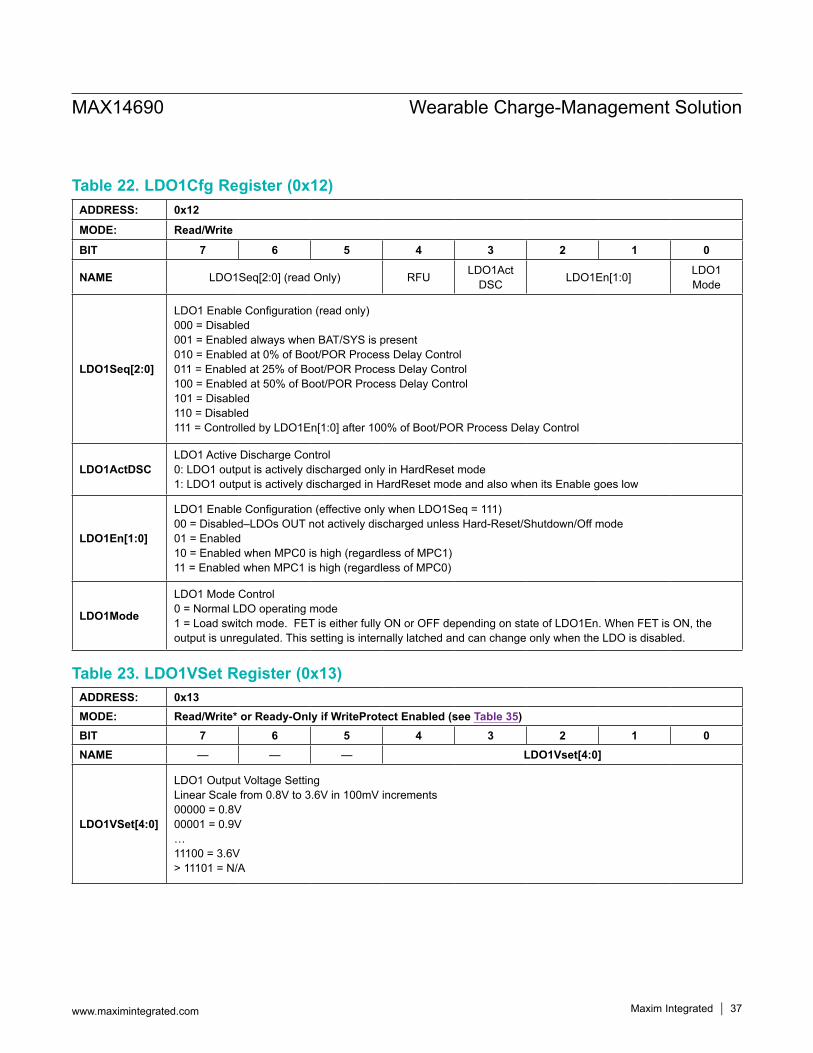
Table 22. LDO1Cfg Register (0x12)
Table 23. LDO1VSet Register (0x13)
ADDRESS: 0x12
MODE: Read/Write
BIT 7 6 5 4 3 2 1 0
NAME LDO1Seq[2:0] (read Only) RFU LDO1Act DSC LDO1En[1:0] LDO1
Mode
LDO1Seq[2:0]
LDO1 Enable Configuration (read only)000 = Disabled001 = Enabled always when BAT/SYS is present010 = Enabled at 0% of Boot/POR Process Delay Control011 = Enabled at 25% of Boot/POR Process Delay Control100 = Enabled at 50% of Boot/POR Process Delay Control 101 = Disabled110 = Disabled111 = Controlled by LDO1En[1:0] after 100% of Boot/POR Process Delay Control
LDO1ActDSCLDO1 Active Discharge Control0: LDO1 output is actively discharged only in HardReset mode1: LDO1 output is actively discharged in HardReset mode and also when its Enable goes low
LDO1En[1:0]
LDO1 Enable Configuration (effective only when LDO1Seq = 111)00 = Disabled–LDOs OUT not actively discharged unless Hard-Reset/Shutdown/Off mode01 = Enabled10 = Enabled when MPC0 is high (regardless of MPC1)11 = Enabled when MPC1 is high (regardless of MPC0)
LDO1Mode
LDO1 Mode Control0 = Normal LDO operating mode1 = Load switch mode. FET is either fully ON or OFF depending on state of LDO1En. When FET is ON, the output is unregulated. This setting is internally latched and can change only when the LDO is disabled.
ADDRESS: 0x13MODE: Read/Write* or Ready-Only if WriteProtect Enabled (see Table 35)BIT 7 6 5 4 3 2 1 0NAME — — — LDO1Vset[4:0]
LDO1VSet[4:0]
LDO1 Output Voltage SettingLinear Scale from 0.8V to 3.6V in 100mV increments00000 = 0.8V00001 = 0.9V…11100 = 3.6V> 11101 = N/A
MAX14690 Wearable Charge-Management Solution
www.maximintegrated.com Maxim Integrated 37

Table 24. LDO2Cfg Register (0x14)
Table 25. LDO2VSet Register (0x15)
ADDRESS: 0x14
MODE: Read/Write
BIT 7 6 5 4 3 2 1 0
NAME LDO2Seq[2:0] (read only) RFU LDO2Act DSC LDO2En[1:0] LDO2
Mode
LDO2Seq [2:0]
LDO2 Enable Configuration (read only)000 = Disabled001 = Enabled always when BAT/SYS is present010 = Enabled at 0% of Boot/POR Process Delay Control011 = Enabled at 25% of Boot/POR Process Delay Control100 = Enabled at 50% of Boot/POR Process Delay Control 101 = Disabled110 = Disabled111 = Controlled by LDO2En[1:0] after 100% of Boot/POR Process Delay Control
LDO2ActDSCLDO2 Active Discharge Control0 = LDO2 output will be actively discharged only in HardReset mode1 = LDO2 output will be actively discharged in HardReset mode and also when its Enable goes Low
LDO2En [1:0]
LDO2 Enable Configuration (effective only when LDO2Seq = 111)00 = Disabled – LDO’s OUT not actively discharged unless HardReset/ShutDown/Off Mode01 = Enabled10 = Enabled when MPC0 is high (regardless of MPC1)11 = Enabled when MPC1 is high (regardless of MPC0)
LDO2Mode
LDO2 Mode Control0 = Normal LDO operating mode1 = Load switch mode. FET is either fully ON or OFF depending on state of LDO2En. When FET is ON, the output is unregulated. This setting is internally latched and can change only when the LDO is disabled.
ADDRESS: 0x15
MODE: Read/Write or Ready-Only if WriteProtect Enabled (see Table 35)
BIT 7 6 5 4 3 2 1 0
NAME — — — LDO2Vset[4:0]
LDO2VSet[4:0]
LDO2 Output Voltage SettingLinear scale from 0.8V to 3.6V in 100mV increments00000 = 0.8V00001 = 0.9V…11100 = 3.6V> 11101 = N/A
MAX14690 Wearable Charge-Management Solution
www.maximintegrated.com Maxim Integrated 38

Table 26. LDO3Cfg Register (0x16)
Table 27. LDO3VSet Register (0x17)
ADDRESS: 0x16
MODE: Read/Write
BIT 7 6 5 4 3 2 1 0
NAME LDO3Seq[2:0] (read-only) RFU LDO3Act DSC LDO3En[1:0] LDO3
Mode
LDO3Seq[2:0]
LDO3 Enable Configuration (read only)000 = Disabled001 = Enabled always when BAT/SYS is present010 = Enabled at 0% of Boot/POR Process Delay Control011 = Enabled at 25% of Boot/POR Process Delay Control100 = Enabled at 50% of Boot/POR Process Delay Control 101 = Disabled110 = Disabled111 = Controlled by LDO3En[1:0] after 100% of Boot/POR Process Delay Control
LDO3ActDSCLDO3 Active Discharge Control0 = LDO3 output is actively discharged only in HardReset mode1 = LDO3 output is actively discharged in HardReset modes and also when its Enable goes low.
LDO3En[1:0]
LDO3 Enable Configuration (effective only when LDO3Seq == 111)00 = Disabled. LDO’s OUT not actively discharged unless in HardReset/ShutDown/Off mode01 = Enabled10 = Enabled when MPC0 is high (regardless of MPC1)11 = Enabled when MPC1 is high (regardless of MPC0)
LDO3Mode
LDO3 Mode Control0 = Normal LDO operating mode1 = Load switch mode. FET is either fully ON or OFF depending on state of LDO3En. When FET is ON, the output is unregulated. This setting is internally latched and can change only when the LDO is disabled.
ADDRESS: 0x17MODE: Read/Write or Ready-Only if WriteProtect Enabled (see Table 35)BIT 7 6 5 4 3 2 1 0NAME — — — LDO3Vset[4:0]
LDO3VSet[4:0]
LDO3 Output Voltage SettingLinear scale from 0.8V to 3.6V in 100mV increments00000 = 0.8V00001 = 0.9V…11100 = 3.6V> 11101 = N/A
MAX14690 Wearable Charge-Management Solution
www.maximintegrated.com Maxim Integrated 39

Table 28. ThrmCfg Register (0x18)
Table 29. MONCfg Register (0x19)
ADDRESS: 0x18MODE: Read/Write* or Ready-Only if WriteProtect Enabled (see Table 35)BIT 7 6 5 4 3 2 1 0NAME — — — — — — JEITAEn ThermEn
JEITAEnThermal or JEITA Monitoring Enable 0 = JEITA monitoring disabled1 = JEITA monitoring enabled, only if ThermEn = 1
ThermEnThermal or JEITA Monitoring Selector 0 = Thermal monitoring disabled1 = Thermal monitoring enabled
ADDRESS: 0x19MODE: Read/WriteBIT 7 6 5 4 3 2 1 0NAME — — MONRatioCfg[1:0] MONtHiZ MONCtr[2:0]
MONRatioCfg
MON Resistive Partition Selector00 = 4:101 = 3:110 = 2:111 = 1:1
MONtHiZMON OFF MODE condition0 = Pulled low by 100k pulldown resistor1 = Hi-Z
MONCtr[2:0]
MON Pin Source selection (40µs BBM after any change of MONCtr)000 = MON is not connected to any internal node and its state depends on MONHiZ001 = MON connected to a resistive partition of BATT010 = MON connected to a resistive partition of SYS011 = MON connected to a resistive partition of BUCK1 OUT100 = MON connected to a resistive partition of BUCK2 OUT101 = MON connected to a resistive partition of LDO1 OUT110 = MON connected to a resistive partition of LDO2 OUT111 = MON connected to a resistive partition of LDO3 OUT
*Register is reset to default value upon CHGIN rising edge.
MAX14690 Wearable Charge-Management Solution
www.maximintegrated.com Maxim Integrated 40

Table 30. BootCfg Register (0x1A)
Table 31. PinStat Register (0x1B)
ADDRESS: 0x1AMODE: Read-OnlyBIT 7 6 5 4 3 2 1 0NAME PwrRstCfg[3:0] SftRstCfg BootDly[1:0] RFU
PwrRstCfg [3:0] See Table 1
SftRstCfgSoft Reset Register Default0 = Registers do not reset to default values on soft reset1 = Registers reset to default values on soft reset
BootDly[1:0]
Boot/POR Process Delay Control00 = 80ms + 34ms01 = 120ms + 34ms10 = 220ms + 34ms11 = 420ms + 34ms
ADDRESS: 0x1B
MODE: Read/Write
BIT 7 6 5 4 3 2 1 0
NAME ILim_T[2:0] — PFN1 PFN2 MPC1 MPC0
ILim_T[2:0]
Monitor of The Input limiter Current Setting000 = Input limiter off001 = 100mA010 = 500mA100 =1A
PFN1PFN1 Input State0 = Pin low1 = Pin high
PFN2PFN2 In/Out State0 = Pin low1 = Pin high
MPC1MPC1 Input State0 = Pin low1 = Pin high
MPC0MPC0 Input State0 = Pin low1 = Pin high
MAX14690 Wearable Charge-Management Solution
www.maximintegrated.com Maxim Integrated 41

Table 32. Buck1/2Extra Control Register (0x1C)
Table 33. PwrCfg Register (0x1D)
Table 34. PwrOff Register (0x1F)
ADDRESS: 0x1C
MODE: Read/Write
BIT 7 6 5 4 3 2 1 0
NAME Reserved Reserved Buck2 ActDSC
Buck2 FFET Reserved Reserved Buck1
ActDSCBuck1 FFET
Buck2ActDSCBuck2 Active Discharge Control0 = Buck2 output is actively discharged only in HardReset mode.1 = Buck2 output is actively discharged in HardReset mode and also when its Enable goes low.
Buck2FFET Buck2 Force FET scaling (it reduces IQ by lowering the nMOS power to 20% of the nominal value)0 = FET Scaling only enabled during the Buck2 turn-on sequence.1 = FET Scaling enabled during the Buck2 turn-on sequence and also in the Buck2 steady on state.
Buck1ActDSCBuck1 Active Discharge Control0 = Buck1 output is actively discharged only in HardReset mode.1 = Buck1 output is actively discharged in HardReset mode and also when its Enable goes low.
Buck1FFET Buck1 Force FET Scaling (it reduces IQ by lowering the nMOS power to 20% of the nominal value)0 = FET Scaling only enabled during the Buck1 turn-on sequence.1 = FET Scaling enabled during the Buck1 turn-on sequence and also in the Buck1 steady on state.
ADDRESS: 0x1D
MODE: Read/Write
BIT 7 6 5 4 3 2 1 0
NAME PFNx ResEna – – – – – – StayOn
PFNxResEnaPFN_ Automatic Internal Pull-Up/Pull-Down Enable0 = No internal pullup/pulldown1 = Automatic internal pullup/pulldown as per Table 1
StayOn
This bit is used to ensure that the processor booted correctly. This bit must be set within 5s of power-on to prevent the part from shutting down and returning to the power-off condition. This bit has no effect after being set.0 = Shut down 5s after power-on1 = Stay on
ADDRESS: 0x1F
MODE: Read/Write
BIT 7 6 5 4 3 2 1 0
NAME PWR_CMD[7:0]
PWR_CMD [7:0]
Power-Off CommandWriting 0xB2 to this register places the part in the off mode except in PwrRstCfg[3:0] modes 0000 and 0001 when it has no effect. Writing any other code has no effect.In PwrRstCfg[3:0] modes 0110 and 0111, the part can be turned back on by a button press or a valid voltage applied to CHGIN. In all other modes, only a valid voltage applied to CHGIN turns the device back on. See Figure 1 for more details.
MAX14690 Wearable Charge-Management Solution
www.maximintegrated.com Maxim Integrated 42
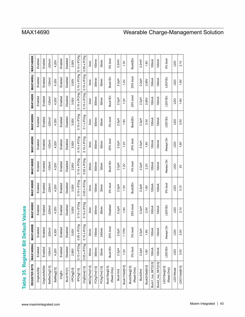
Tabl
e 35
. Reg
iste
r Bit
Def
ault
Valu
esR
EGIS
TER
BIT
SM
AX1
4690
AM
AX1
4690
BM
AX1
4690
CM
AX1
4690
DM
AX1
4690
EM
AX1
4690
NM
AX1
4690
HM
AX1
4690
IM
AX1
4690
JM
AX1
4690
K
Chg
Aut
oStp
Ena
bled
Ena
bled
Ena
bled
Ena
bled
Ena
bled
Ena
bled
Ena
bled
Ena
bled
Ena
bled
Ena
bled
Chg
Aut
oReS
taE
nabl
edE
nabl
edE
nabl
edE
nabl
edE
nabl
edE
nabl
edE
nabl
edE
nabl
edE
nabl
edE
nabl
ed
Bat
ReC
hg[1
:0]
-120
mV
-220
mV
-220
mV
-220
mV
-120
mV
-120
mV
-220
mV
-120
mV
-120
mV
-220
mV
Bat
Reg
[2:0
]4.
20V
4.30
V4.
35V
4.20
V4.
20V
4.20
V4.
35V
4.20
V4.
35V
4.20
V
Chg
En
Ena
bled
Ena
bled
Ena
bled
Ena
bled
Ena
bled
Ena
bled
Ena
bled
Ena
bled
Ena
bled
Ena
bled
Buc
k1E
n[1]
Dis
able
dD
isab
led
Dis
able
dD
isab
led
Dis
able
dD
isab
led
Dis
able
dD
isab
led
Dis
able
dD
isab
led
VP
Chg
[2:0
]2.
85V
3.00
V3.
00V
3.00
V2.
85V
3.00
V3.
00V
3.00
V3.
00V
3.00
V
IPC
hg[1
:0]
0.10
x IF
Chg
0.05
x IF
Chg
0.10
x IF
Chg
0.10
x IF
Chg
0.10
x IF
Chg
0.10
x IF
Chg
0.10
x IF
Chg
0.10
x IF
CH
g0.
10 x
IFC
Hg
0.10
x IF
CH
g
Chg
Don
e[1:
0]0.
05 x
IFC
hg0.
10 x
IFC
hg0.
10 x
IFC
hg0.
05 x
IFC
hg0.
05 x
IFC
hg0.
10 x
IFC
hg0.
1 x
IFC
hg0.
10 x
IFC
hg0.
10 x
IFC
hg0.
05 x
IFC
hg
MtC
hgTm
r[1:0
]60
min
30m
in0m
in0m
in60
min
0min
0min
0min
0min
0min
FChg
Tmr[1
:0]
300m
in15
0min
300m
in15
0min
600m
in30
0min
300m
in30
0min
300m
in15
0min
PC
hgTm
r[1:0
]30
min
240m
in60
min
30m
in30
min
60m
in60
min
60m
in60
min
30m
in
Buc
k1S
eq[2
:0]
(Rea
d-O
nly)
Buc
k1E
n25
% b
oot
Dis
able
d0%
boo
tB
uck1
En
25%
boo
t0%
boo
tB
uck1
En
Buc
k1E
n0%
boo
t
Buc
k1In
d2.
2μH
2.2μ
H2.
2μH
2.2μ
H2.
2μH
2.2μ
H2.
2μH
2.2μ
H2.
2μH
2.2m
H
Buc
k1V
Set
[5:0
]1.
2V1.
175V
1.8V
1.3V
1.2V
1.2V
1.8V
1.2V
1.2V
1.3V
Buc
k2S
eq[2
:0]
(Rea
d-O
nly)
0% b
oot
0% b
oot
25%
boo
tB
uck2
En
0% b
oot
25%
boo
tB
uck2
En
25%
boo
t25
% b
oot
Buc
k2E
n
Buc
k2In
d2.
2μH
2.2μ
H2.
2μH
2.2μ
H2.
2μH
2.2μ
H2.
2μH
2.2μ
H2.
2μH
2.2m
H
Buc
k2V
Set
[5:0
]1.
8V1.
8V2.
0V1.
8V2.
2V1.
8V3.
3V2.
85V
2.85
V1.
8V
Buc
k1_I
up_S
ET[
2:0]
100m
A10
0mA
100m
A10
0mA
100m
A10
0mA
100m
A10
0mA
100m
A10
0mA
Buc
k2_I
up_S
ET[
2:0]
100m
A10
0mA
100m
A10
0mA
100m
A10
0mA
100m
A10
0mA
100m
A10
0mA
LDO
1Seq
[2:0
] (R
ead-
Onl
y)LD
O1E
nA
lway
s O
nLD
O1E
n0%
boo
tA
lway
s O
nA
lway
s O
nLD
O1E
nLD
O1E
nLD
O1E
n0%
boo
t
LDO
1Mod
eLD
OLD
OLD
OLD
OLD
OLD
OLD
OLD
OLD
OLD
O
LDO
1Vse
t[4:0
]3.
0V2.
0V3.
1V3.
1V2V
1.8V
3.0V
1.8V
1.8V
3.1V
MAX14690 Wearable Charge-Management Solution
www.maximintegrated.com Maxim Integrated 43

REG
ISTE
R B
ITS
MA
X146
90A
MA
X146
90B
MA
X146
90C
MA
X146
90D
MA
X146
90E
MA
X146
90N
MA
X146
90H
MA
X146
90I
MA
X146
90J
MA
X146
90K
LDO
2Seq
[2:0
] (R
ead-
Onl
y)LD
O2E
nLD
O2E
nLD
O2E
nLD
O2E
nLD
O2E
nLD
O2E
nLD
O2E
nLD
O2E
nLD
O2E
nLD
O2E
n
LDO
2Mod
eS
witc
hLD
OLD
OS
witc
hLD
OLD
OLD
OLD
OLD
OS
witc
h
LDO
2Vse
t[4:0
]3.
7V3.
2V1.
8V0.
8V2.
7V3.
2V3.
0V1.
2V1.
2V0.
8V
LDO
3Seq
[2:0
] (R
ead-
Onl
y)LD
O3E
nLD
O3E
nLD
O3E
nLD
O3E
nLD
O3E
nLD
O3E
nLD
O3E
nLD
O3E
nLD
O3E
nLD
O3E
n
LDO
3Mod
eS
witc
hS
witc
hS
witc
hS
witc
hS
witc
hLD
OLD
OLD
OLD
OS
witc
h
LDO
3Vse
t[4:0
]3.
7V3.
7V1.
8V0.
8V3.
7V3.
0V3.
0V3V
3V0.
8V
JEIT
AE
nD
isab
led
Ena
bled
Ena
bled
Dis
able
dE
nabl
edD
isab
led
Ena
bled
Dis
able
dD
isab
led
Dis
able
d
Ther
mE
nE
nabl
edE
nabl
edE
nabl
edE
nabl
edE
nabl
edE
nabl
edE
nabl
edE
nabl
edE
nabl
edE
nabl
ed
Pw
rRst
Cfg
[3:0
] (R
ead-
Onl
y)K
IN#
KIN
#S
oft R
eset
CR
Low
Sof
t Res
etK
INK
INS
oft R
eset
Sof
t Res
etS
oft R
eset
SftR
stC
fg
(Rea
d-O
nly)
Hol
dR
eset
Res
etR
eset
Hol
dH
old
Res
etH
old
Hol
dR
eset
Boo
tDly
[1:0
] (R
ead-
Onl
y)(1
20 +
34)
ms
(80
+ 34
)ms
(120
+ 3
4)m
s(8
0 +
34)m
s(8
0 +
34)m
s(1
20 +
34)
ms
(120
+ 3
4)m
s(1
20 +
34)
ms
(120
+ 3
4)m
s(8
0 +
34)m
s
PFN
xRes
Ena
Ena
bled
Ena
bled
Ena
bled
Ena
bled
Ena
bled
Ena
bled
Ena
bled
Ena
bled
Ena
bled
Ena
bled
Sta
yOn
5s T
urno
ffS
tay
On
Sta
y O
nS
tay
On
Sta
y O
nS
tay
On
Sta
y O
nS
tay
On
Sta
y O
nS
tay
On
Writ
ePro
tect
Writ
able
Writ
able
Writ
able
Writ
able
Writ
able
Writ
able
Writ
able
Writ
able
Writ
able
Writ
able
ILim
Cnt
l[1:0
]50
0mA
500m
A50
0mA
500m
A50
0mA
500m
A50
0mA
500m
A10
0mA
500m
A
Tabl
e 35
. Reg
iste
r Bit
Def
ault
Valu
es (c
ontin
ued)
MAX14690 Wearable Charge-Management Solution
www.maximintegrated.com Maxim Integrated 44

Tabl
e 36
. Reg
iste
r Def
ault
Valu
esR
EGIS
TER
A
DD
RES
SR
EGIS
TER
N
AM
ED
EFA
ULT
VA
LUES
MAX
1469
0AM
AX14
690B
MAX
1469
0CM
AX14
690D
MAX
1469
0EM
AX14
690N
MAX
1469
0HM
AX1
4690
IMAX
1469
0JM
AX14
690K
0x00
Chi
pId
0x01
0x01
0x01
0x01
0x01
0x01
0x01
0x01
0x01
0x01
0x01
Chi
pRev
0x02
0x02
0x03
0x02
0x03
0x03
0x03
0x03
0x02
0x02
0x07
IntM
askA
0x00
0x00
0x00
0x00
0x00
0x00
0x00
0x00
0x00
0x00
0x08
IntM
askB
0x00
0x00
0x00
0x00
0x00
0x00
0x00
0x00
0x00
0x00
0x09
ILim
Cnt
l0x
020x
020x
020x
020x
020x
020x
020x
020x
010x
02
0x0A
Chg
Cnt
lA0x
D7
0xFB
0xFD
0xF7
0xD
70x
D7
0xFD
0xD
70x
DD
0xF7
0x0B
Chg
Cnt
lB0x
540x
610x
650x
640x
540x
650x
650x
650x
650x
64
0x0C
Chg
Tmr
0x38
0x27
0x09
0x04
0x3C
0x09
0x09
0x09
0x09
0x04
0x0D
Buc
k1C
fg0x
E0
0x60
0x00
0x40
0xE
00x
600x
400x
E0
0xE
00x
40
0x0E
Buc
k1V
Set
0x10
0x0F
0x28
0x14
0x10
0x10
0x28
0x10
0x10
0x14
0x0F
Buc
k2C
fg0x
400x
400x
600x
E0
0x40
0x60
0xE
00x
600x
600x
E0
0x10
Buc
k2V
Set
0x06
0x06
0x0A
0x06
0x0E
0x06
0x24
0x1B
0x1B
0x06
0x11
Res
erve
d0x
240x
240x
240x
240x
240x
240x
240x
240x
240x
24
0x12
LDO
1Cfg
0xE
00x
200x
E0
0x40
0x20
0x20
0xE
00x
E0
0xE
00x
40
0x13
LDO
1VS
et0x
160x
0C0x
170x
170x
0C0x
0A0x
160x
0A0x
0A0x
17
0x14
LDO
2Cfg
0xE
10x
E0
0xE
00x
E1
0xE
00x
E0
0xE
00x
E0
0xE
00x
E1
0x15
LDO
2VS
et0x
1D0x
180x
0A0x
000x
130x
180x
160x
040x
040x
00
0x16
LDO
3Cfg
0xE
10x
E1
0xE
10x
E1
0xE
10x
E0
0xE
00x
E0
0xE
00x
E1
0x17
LDO
3VS
et0x
1D0x
1D0x
0A0x
000x
1D0x
160x
160x
160x
160x
00
0x18
Thrm
Cfg
0x01
0x03
0x03
0x01
0x03
0x01
0x03
0x01
0x01
0x01
0x19
MO
NC
fg0x
000x
000x
000x
000x
000x
000x
000x
000x
000x
00
0x1A
Boo
tCfg
0x63
0x69
0x7B
0x59
0x71
0x63
0x6B
0x73
0x73
0x79
0x1C
Buck
1/2E
xtra
0x00
0x00
0x00
0x00
0x00
0x00
0x00
0x00
0x00
0x00
0x1D
Pw
rCfg
0x80
0x81
0x81
0x81
0x81
0x81
0x81
0x81
0x81
0x81
0x1E
NU
LL0x
000x
000x
000x
000x
000x
000x
000x
000x
000x
00
0x1F
Pw
rOff
0x00
0x00
0x00
0x00
0x00
0x00
0x00
0x00
0x00
0x00
MAX14690 Wearable Charge-Management Solution
www.maximintegrated.com Maxim Integrated 45

+Denotes a lead(Pb)-free package/RoHS-compliant package. T = Tape and reel. *Future Product—contact marketing for availability. See Table 35 and Table 36 for the device differences.
PART TEMP RANGE PIN-PACKAGE
MAX14690AEWX+ -40°C to +85°C 36 WLP
MAX14690AEWX+T -40°C to +85°C 36 WLP
MAX14690BEWX+ -40°C to +85°C 36 WLP
MAX14690BEWX+T -40°C to +85°C 36 WLP
MAX14690CEWX+ -40°C to +85°C 36 WLP
MAX14690CEWX+T -40°C to +85°C 36 WLP
MAX14690DEWX+ -40°C to +85°C 36 WLP
MAX14690DEWX+T -40°C to +85°C 36 WLP
MAX14690EEWX+* -40°C to +85°C 36 WLP
MAX14690EEWX+T* -40°C to +85°C 36 WLP
MAX14690HEWX+ -40°C to +85°C 36 WLP
MAX14690HEWX+T -40°C to +85°C 36 WLP
MAX14690IEWX+ -40°C to +85°C 36 WLP
MAX14690IEWX+T -40°C to +85°C 36 WLP
MAX14690JEWX+ -40°C to +85°C 36 WLP
MAX14690JEWX+T -40°C to +85°C 36 WLP
MAX14690KEWX+* -40°C to +85°C 36 WLP
MAX14690KEWX+T* -40°C to +85°C 36 WLP
MAX14690NEWX+ -40°C to +85°C 36 WLP
MAX14690NEWX+T -40°C to +85°C 36 WLP
PACKAGE TYPE
PACKAGE CODE
OUTLINE NO.
LAND PATTERN NO.
36 WLP W362D2+1 21-0897Refer to
Application Note 1891
MAX14690 Wearable Charge-Management Solution
www.maximintegrated.com Maxim Integrated 46
Chip InformationPROCESS: BiCMOS
Ordering Information
Package InformationFor the latest package outline information and land patterns (footprints), go to www.maximintegrated.com/packages. Note that a “+”, “#”, or “-” in the package code indicates RoHS status only. Package drawings may show a different suffix character, but the drawing pertains to the package regardless of RoHS status.

REVISIONNUMBER
REVISIONDATE DESCRIPTION PAGES
CHANGED
0 12/14 Initial release —
1 4/15 BUCK1 default was changed to 1.175V from 2.0V 6, 13, 15, 16, 19, 22, 40
2 4/15 Removed future product designation from MAX14690AEWX+ 413 4/15 Added additional Buck Ripple specifications in Electrical Characteristics table 5, 6
4 5/15 Added I2C section and MAX14690C/D/N as future products2, 11, 17-18, 22, 24,
39-42
5 7/15 Removed future product designation from MAX14690DEWX+ and MAX14690DEWX+T 45
6 10/15 Removed future product designation of MAX14690C and MAX14690N 2, 10, 13, 18, 29, 41-45
7 1/16 Added MAX14690I part numbers to data sheet 5, 11, 18, 43–458 2/16 Push Button Control diagram updated 189 2/16 Removed future product designation from MAX14690I 45
10 4/16 Removed future product designation from MAX14690H and added MAX14690J to Ordering Information table 43-45
11 5/16 Added MAX14690K future product 43-45
Maxim Integrated cannot assume responsibility for use of any circuitry other than circuitry entirely embodied in a Maxim Integrated product. No circuit patent licenses are implied. Maxim Integrated reserves the right to change the circuitry and specifications without notice at any time. The parametric values (min and max limits) shown in the Electrical Characteristics table are guaranteed. Other parametric values quoted in this data sheet are provided for guidance.
Maxim Integrated and the Maxim Integrated logo are trademarks of Maxim Integrated Products, Inc.
MAX14690 Wearable Charge-Management Solution
© 2016 Maxim Integrated Products, Inc. 47
Revision History
For pricing, delivery, and ordering information, please contact Maxim Direct at 1-888-629-4642, or visit Maxim Integrated’s website at www.maximintegrated.com.