max14745 wearable carge-management soltion · general description the max14745 is a...
TRANSCRIPT

General DescriptionThe MAX14745 is a battery-charge-management solution ideal for low-power wearable applications. The device includes a linear battery charger with a smart power selector and several power-optimized peripherals. The MAX14745 features two ultra-low quiescent current buck regulators and three ultra-low quiescent current low-dropout (LDO) linear regulators, providing up to five regulated voltages, each with an ultra-low quiescent current, allows designers to minimize power consumption and extend battery life in 24/7 operation devices, such as those in the wearable market.The battery charger features a smart power selector that allows operation on a dead battery when connected to a power source. To avoid overloading a power adapter, the input current to the smart power selector is limited based on an I2C register setting. If the charger power source is unable to supply the entire system load, the smart power control circuit supplements the system load with current from the battery. The charger also supports temperature dependent charge currents.The two synchronous, high-efficiency step-down buck regulators feature a variable frequency mode for increased efficiency during light-load operation. The output voltage of these regulators can be programmed through I2C with the default preconfigured. The buck regulators can support dynamic voltage scaling to further improve system power consumption.The three configurable LDOs each have a dedicated input pin. Each LDO regulator output voltage can be programmed through I2C with the default preconfigured. The linear regulators can also be configured to operate as power switches that may be used to disconnect the quiescent load of the system peripherals. The MAX14745 features a programmable power controller that allows the device to be configured for applications that require the device be in a true-off, or always-on, state. The controller also provides a delayed reset signal and voltage sequencing. The MAX14745 is available in a 36-bump, 0.4mm pitch, 2.72mm x 2.47mm wafer-level package (WLP).
Benefits and Features Extend System Use Time Between Battery Charging
• Dual Ultra-Low-IQ 200mA Buck Regulators - Output Programmable from 0.8V to 2.375V and 0.8V to 3.95V
- 0.9μA (typ) Quiescent Current (Buck 1) - Optional Fixed Peak-Current Mode to Optimize Ripple Frequency in Noise-Sensitive Applications
• Three Ultra-Low-IQ 100mA LDOs• LDO1
- Output Programmable from 0.8V to 3.6V - 0.6μA (typ) Quiescent Current - 2.7V to 5.5V Input with Dedicated Pin
• LDO2/3 - Output Programmable from 0.9V to 4V - 1μA (typ) Quiescent Current - 1.71V to 5.5V Input with Dedicated Pin
Easy-to-Implement Li+ Battery Charging• Smart Power Selector• 28V/-5.5V Tolerant Input• Thermistor Monitor
Minimize Solution Footprint Through High Integration• Provides Five Regulated Voltage Rails• Switch Mode Option on Each LDO
Optimize System Control• Monitors Pushbutton for Ultra-Low Power Mode• Power-On Reset Delay and Voltage Sequencing• On-Chip Voltage Monitor Multiplexer
Applications Wearable Electronics Fitness Monitors Rechargeable IoT devices
19-8560; Rev 10; 4/18
Ordering Information appears at end of data sheet.
MAX14745 Wearable Charge-Management Solution
EVALUATION KIT AVAILABLE
Click here for production status of specific part numbers.
MAX14745 Wearable Charge-Management Solution
www.maximintegrated.com Maxim Integrated 2
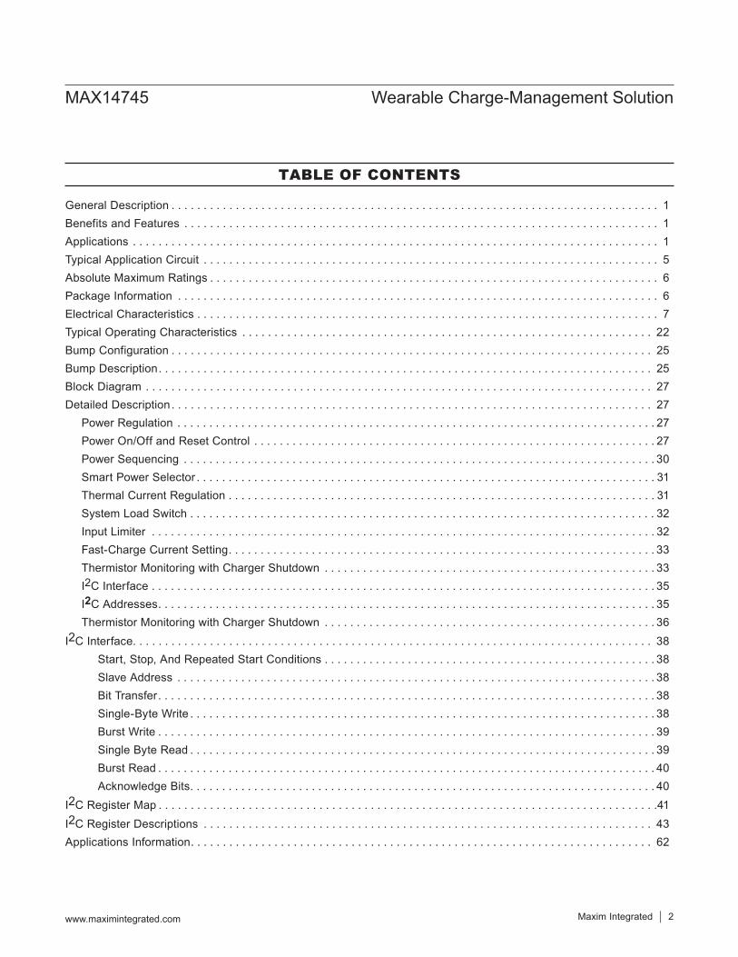
TABLE OF CONTENTS
General Description . . . . . . . . . . . . . . . . . . . . . . . . . . . . . . . . . . . . . . . . . . . . . . . . . . . . . . . . . . . . . . . . . . . . . . . . . . . . 1Benefits and Features . . . . . . . . . . . . . . . . . . . . . . . . . . . . . . . . . . . . . . . . . . . . . . . . . . . . . . . . . . . . . . . . . . . . . . . . . . 1Applications . . . . . . . . . . . . . . . . . . . . . . . . . . . . . . . . . . . . . . . . . . . . . . . . . . . . . . . . . . . . . . . . . . . . . . . . . . . . . . . . . . 1Typical Application Circuit . . . . . . . . . . . . . . . . . . . . . . . . . . . . . . . . . . . . . . . . . . . . . . . . . . . . . . . . . . . . . . . . . . . . . . . 5Absolute Maximum Ratings . . . . . . . . . . . . . . . . . . . . . . . . . . . . . . . . . . . . . . . . . . . . . . . . . . . . . . . . . . . . . . . . . . . . . . 6Package Information . . . . . . . . . . . . . . . . . . . . . . . . . . . . . . . . . . . . . . . . . . . . . . . . . . . . . . . . . . . . . . . . . . . . . . . . . . . 6Electrical Characteristics . . . . . . . . . . . . . . . . . . . . . . . . . . . . . . . . . . . . . . . . . . . . . . . . . . . . . . . . . . . . . . . . . . . . . . . . 7Typical Operating Characteristics . . . . . . . . . . . . . . . . . . . . . . . . . . . . . . . . . . . . . . . . . . . . . . . . . . . . . . . . . . . . . . . . 22Bump Configuration . . . . . . . . . . . . . . . . . . . . . . . . . . . . . . . . . . . . . . . . . . . . . . . . . . . . . . . . . . . . . . . . . . . . . . . . . . . 25Bump Description. . . . . . . . . . . . . . . . . . . . . . . . . . . . . . . . . . . . . . . . . . . . . . . . . . . . . . . . . . . . . . . . . . . . . . . . . . . . . 25Block Diagram . . . . . . . . . . . . . . . . . . . . . . . . . . . . . . . . . . . . . . . . . . . . . . . . . . . . . . . . . . . . . . . . . . . . . . . . . . . . . . . 27Detailed Description. . . . . . . . . . . . . . . . . . . . . . . . . . . . . . . . . . . . . . . . . . . . . . . . . . . . . . . . . . . . . . . . . . . . . . . . . . . 27
Power Regulation . . . . . . . . . . . . . . . . . . . . . . . . . . . . . . . . . . . . . . . . . . . . . . . . . . . . . . . . . . . . . . . . . . . . . . . . . . . 27Power On/Off and Reset Control . . . . . . . . . . . . . . . . . . . . . . . . . . . . . . . . . . . . . . . . . . . . . . . . . . . . . . . . . . . . . . . 27Power Sequencing . . . . . . . . . . . . . . . . . . . . . . . . . . . . . . . . . . . . . . . . . . . . . . . . . . . . . . . . . . . . . . . . . . . . . . . . . . 30Smart Power Selector . . . . . . . . . . . . . . . . . . . . . . . . . . . . . . . . . . . . . . . . . . . . . . . . . . . . . . . . . . . . . . . . . . . . . . . . 31Thermal Current Regulation . . . . . . . . . . . . . . . . . . . . . . . . . . . . . . . . . . . . . . . . . . . . . . . . . . . . . . . . . . . . . . . . . . . 31System Load Switch . . . . . . . . . . . . . . . . . . . . . . . . . . . . . . . . . . . . . . . . . . . . . . . . . . . . . . . . . . . . . . . . . . . . . . . . . 32Input Limiter . . . . . . . . . . . . . . . . . . . . . . . . . . . . . . . . . . . . . . . . . . . . . . . . . . . . . . . . . . . . . . . . . . . . . . . . . . . . . . . 32Fast-Charge Current Setting. . . . . . . . . . . . . . . . . . . . . . . . . . . . . . . . . . . . . . . . . . . . . . . . . . . . . . . . . . . . . . . . . . . 33Thermistor Monitoring with Charger Shutdown . . . . . . . . . . . . . . . . . . . . . . . . . . . . . . . . . . . . . . . . . . . . . . . . . . . . 33I2C Interface . . . . . . . . . . . . . . . . . . . . . . . . . . . . . . . . . . . . . . . . . . . . . . . . . . . . . . . . . . . . . . . . . . . . . . . . . . . . . . . 35I2C Addresses. . . . . . . . . . . . . . . . . . . . . . . . . . . . . . . . . . . . . . . . . . . . . . . . . . . . . . . . . . . . . . . . . . . . . . . . . . . . . . 35Thermistor Monitoring with Charger Shutdown . . . . . . . . . . . . . . . . . . . . . . . . . . . . . . . . . . . . . . . . . . . . . . . . . . . . 36
I2C Interface. . . . . . . . . . . . . . . . . . . . . . . . . . . . . . . . . . . . . . . . . . . . . . . . . . . . . . . . . . . . . . . . . . . . . . . . . . . . . . . . . 38Start, Stop, And Repeated Start Conditions . . . . . . . . . . . . . . . . . . . . . . . . . . . . . . . . . . . . . . . . . . . . . . . . . . . . 38Slave Address . . . . . . . . . . . . . . . . . . . . . . . . . . . . . . . . . . . . . . . . . . . . . . . . . . . . . . . . . . . . . . . . . . . . . . . . . . . 38Bit Transfer. . . . . . . . . . . . . . . . . . . . . . . . . . . . . . . . . . . . . . . . . . . . . . . . . . . . . . . . . . . . . . . . . . . . . . . . . . . . . . 38Single-Byte Write . . . . . . . . . . . . . . . . . . . . . . . . . . . . . . . . . . . . . . . . . . . . . . . . . . . . . . . . . . . . . . . . . . . . . . . . . 38Burst Write . . . . . . . . . . . . . . . . . . . . . . . . . . . . . . . . . . . . . . . . . . . . . . . . . . . . . . . . . . . . . . . . . . . . . . . . . . . . . . 39Single Byte Read . . . . . . . . . . . . . . . . . . . . . . . . . . . . . . . . . . . . . . . . . . . . . . . . . . . . . . . . . . . . . . . . . . . . . . . . . 39Burst Read . . . . . . . . . . . . . . . . . . . . . . . . . . . . . . . . . . . . . . . . . . . . . . . . . . . . . . . . . . . . . . . . . . . . . . . . . . . . . . 40Acknowledge Bits. . . . . . . . . . . . . . . . . . . . . . . . . . . . . . . . . . . . . . . . . . . . . . . . . . . . . . . . . . . . . . . . . . . . . . . . . 40
I2C Register Map . . . . . . . . . . . . . . . . . . . . . . . . . . . . . . . . . . . . . . . . . . . . . . . . . . . . . . . . . . . . . . . . . . . . . . . . . . . . . .41I2C Register Descriptions . . . . . . . . . . . . . . . . . . . . . . . . . . . . . . . . . . . . . . . . . . . . . . . . . . . . . . . . . . . . . . . . . . . . . . 43Applications Information. . . . . . . . . . . . . . . . . . . . . . . . . . . . . . . . . . . . . . . . . . . . . . . . . . . . . . . . . . . . . . . . . . . . . . . . 62

MAX14745 Wearable Charge-Management Solution
www.maximintegrated.com Maxim Integrated 3
TABLE OF CONTENTS (continued)Inductor Selection . . . . . . . . . . . . . . . . . . . . . . . . . . . . . . . . . . . . . . . . . . . . . . . . . . . . . . . . . . . . . . . . . . . . . . . . . . . 62Output Capacitor Selection. . . . . . . . . . . . . . . . . . . . . . . . . . . . . . . . . . . . . . . . . . . . . . . . . . . . . . . . . . . . . . . . . . . . 62Input Capacitor Selection . . . . . . . . . . . . . . . . . . . . . . . . . . . . . . . . . . . . . . . . . . . . . . . . . . . . . . . . . . . . . . . . . . . . . 62PCB Layout and Routing . . . . . . . . . . . . . . . . . . . . . . . . . . . . . . . . . . . . . . . . . . . . . . . . . . . . . . . . . . . . . . . . . . . . . 62
Ordering Information . . . . . . . . . . . . . . . . . . . . . . . . . . . . . . . . . . . . . . . . . . . . . . . . . . . . . . . . . . . . . . . . . . . . . . . . . . 66Chip Information. . . . . . . . . . . . . . . . . . . . . . . . . . . . . . . . . . . . . . . . . . . . . . . . . . . . . . . . . . . . . . . . . . . . . . . . . . . . . . 66Revision History . . . . . . . . . . . . . . . . . . . . . . . . . . . . . . . . . . . . . . . . . . . . . . . . . . . . . . . . . . . . . . . . . . . . . . . . . . . . . . 67
LIST OF FIGURES
LIST OF TABLES
Table 1. Power Function Input Control Modes. . . . . . . . . . . . . . . . . . . . . . . . . . . . . . . . . . . . . . . . . . . . . . . . . . . . . . . 28Table 2. Thermistor Monitoring/JEITA Monitoring Enable Control. . . . . . . . . . . . . . . . . . . . . . . . . . . . . . . . . . . . . . . . 35
Table 3. I2C Slave Addresses . . . . . . . . . . . . . . . . . . . . . . . . . . . . . . . . . . . . . . . . . . . . . . . . . . . . . . . . . . . . . . . . . . . 38Table 4. ChipId Register (0x00) . . . . . . . . . . . . . . . . . . . . . . . . . . . . . . . . . . . . . . . . . . . . . . . . . . . . . . . . . . . . . . . . . . 43Table 5. ChipRev Register (0x01) . . . . . . . . . . . . . . . . . . . . . . . . . . . . . . . . . . . . . . . . . . . . . . . . . . . . . . . . . . . . . . . . 43Table 6. StatusA Register (0x02) . . . . . . . . . . . . . . . . . . . . . . . . . . . . . . . . . . . . . . . . . . . . . . . . . . . . . . . . . . . . . . . . . 43Table 7. StatusB Register (0x03) . . . . . . . . . . . . . . . . . . . . . . . . . . . . . . . . . . . . . . . . . . . . . . . . . . . . . . . . . . . . . . . . . 44
Figure 1. Power Function Input Control Modes Flow Diagrams . . . . . . . . . . . . . . . . . . . . . . . . . . . . . . . . . . . . . . . . . 29Figure 2a. Power-On Sequencing . . . . . . . . . . . . . . . . . . . . . . . . . . . . . . . . . . . . . . . . . . . . . . . . . . . . . . . . . . . . . . . . 30Figure 2b. Power-On Sequencing Without Battery . . . . . . . . . . . . . . . . . . . . . . . . . . . . . . . . . . . . . . . . . . . . . . . . . . . 31Figure 3. Smart Power Selector Current/Voltage Behavior. . . . . . . . . . . . . . . . . . . . . . . . . . . . . . . . . . . . . . . . . . . . . 32Figure 4a. Charging Behavior Using Thermistor Monitoring Mode . . . . . . . . . . . . . . . . . . . . . . . . . . . . . . . . . . . . . . . 34Figure 4b. Charging Behavior Using JEITA Monitoring 1 and 2 Modes . . . . . . . . . . . . . . . . . . . . . . . . . . . . . . . . . . . 34Figure 5a. Charger State Diagram (Thermistor Monitoring with Charger Shutdown) . . . . . . . . . . . . . . . . . . . . . . . . . 36Figure 5b. Battery Charger State Diagram (JEITA Monitoring with Charger Shutdown). . . . . . . . . . . . . . . . . . . . . . . 37Figure 6. I2C START, STOP and REPEATED START Conditions . . . . . . . . . . . . . . . . . . . . . . . . . . . . . . . . . . . . . . . 38Figure 7. Write Byte Sequence . . . . . . . . . . . . . . . . . . . . . . . . . . . . . . . . . . . . . . . . . . . . . . . . . . . . . . . . . . . . . . . . . . 38Figure 8. Burst Write Sequence. . . . . . . . . . . . . . . . . . . . . . . . . . . . . . . . . . . . . . . . . . . . . . . . . . . . . . . . . . . . . . . . . . 39Figure 9. Read Byte Sequence . . . . . . . . . . . . . . . . . . . . . . . . . . . . . . . . . . . . . . . . . . . . . . . . . . . . . . . . . . . . . . . . . . 39Figure 10. Burst Read Sequence. . . . . . . . . . . . . . . . . . . . . . . . . . . . . . . . . . . . . . . . . . . . . . . . . . . . . . . . . . . . . . . . . 40Figure 11. Acknowledge . . . . . . . . . . . . . . . . . . . . . . . . . . . . . . . . . . . . . . . . . . . . . . . . . . . . . . . . . . . . . . . . . . . . . . . . 40

MAX14745 Wearable Charge-Management Solution
www.maximintegrated.com Maxim Integrated 4
LIST OF TABLES (continued)Table 8. StatusC Register (0x04) . . . . . . . . . . . . . . . . . . . . . . . . . . . . . . . . . . . . . . . . . . . . . . . . . . . . . . . . . . . . . . . . . 45Table 9. IntA Register (0x05) . . . . . . . . . . . . . . . . . . . . . . . . . . . . . . . . . . . . . . . . . . . . . . . . . . . . . . . . . . . . . . . . . . . . 46Table 10. IntB Register (0x06) . . . . . . . . . . . . . . . . . . . . . . . . . . . . . . . . . . . . . . . . . . . . . . . . . . . . . . . . . . . . . . . . . . . 46Table 11. IntMaskA Register (0x07) . . . . . . . . . . . . . . . . . . . . . . . . . . . . . . . . . . . . . . . . . . . . . . . . . . . . . . . . . . . . . . . 47Table 12. IntMaskB Register (0x08). . . . . . . . . . . . . . . . . . . . . . . . . . . . . . . . . . . . . . . . . . . . . . . . . . . . . . . . . . . . . . . 48Table 13. ILimCntl Register (0x09). . . . . . . . . . . . . . . . . . . . . . . . . . . . . . . . . . . . . . . . . . . . . . . . . . . . . . . . . . . . . . . . 48Table 14. ChgCntlA Register (0x0A) . . . . . . . . . . . . . . . . . . . . . . . . . . . . . . . . . . . . . . . . . . . . . . . . . . . . . . . . . . . . . . 49Table 15. ChgCntlB Register (0x0B) . . . . . . . . . . . . . . . . . . . . . . . . . . . . . . . . . . . . . . . . . . . . . . . . . . . . . . . . . . . . . . 50Table 16. ChTmr Register (0x0C) . . . . . . . . . . . . . . . . . . . . . . . . . . . . . . . . . . . . . . . . . . . . . . . . . . . . . . . . . . . . . . . . . 51Table 17. Buck1Cfg Register (0x0D) . . . . . . . . . . . . . . . . . . . . . . . . . . . . . . . . . . . . . . . . . . . . . . . . . . . . . . . . . . . . . . 51Table 18. Buck1VSet Register (0x0E) . . . . . . . . . . . . . . . . . . . . . . . . . . . . . . . . . . . . . . . . . . . . . . . . . . . . . . . . . . . . . 52Table 19. Buck2Cfg Register (0x0F) . . . . . . . . . . . . . . . . . . . . . . . . . . . . . . . . . . . . . . . . . . . . . . . . . . . . . . . . . . . . . . 52Table 20. Buck2VSet Register (0x10) . . . . . . . . . . . . . . . . . . . . . . . . . . . . . . . . . . . . . . . . . . . . . . . . . . . . . . . . . . . . . 53Table 21. Buck1/2ISet Register (0x11) . . . . . . . . . . . . . . . . . . . . . . . . . . . . . . . . . . . . . . . . . . . . . . . . . . . . . . . . . . . . . 53Table 22. LDO1Cfg Register (0x12) . . . . . . . . . . . . . . . . . . . . . . . . . . . . . . . . . . . . . . . . . . . . . . . . . . . . . . . . . . . . . . . 54Table 23. LDO1VSet Register (0x13) . . . . . . . . . . . . . . . . . . . . . . . . . . . . . . . . . . . . . . . . . . . . . . . . . . . . . . . . . . . . . . 54Table 24. LDO2Cfg Register (0x14) . . . . . . . . . . . . . . . . . . . . . . . . . . . . . . . . . . . . . . . . . . . . . . . . . . . . . . . . . . . . . . . 55Table 25. LDO2VSet Register (0x15). . . . . . . . . . . . . . . . . . . . . . . . . . . . . . . . . . . . . . . . . . . . . . . . . . . . . . . . . . . . . . 55Table 26. LDO3Cfg Register (0x16) . . . . . . . . . . . . . . . . . . . . . . . . . . . . . . . . . . . . . . . . . . . . . . . . . . . . . . . . . . . . . . . 56Table 27. LDO3VSet Register (0x17) . . . . . . . . . . . . . . . . . . . . . . . . . . . . . . . . . . . . . . . . . . . . . . . . . . . . . . . . . . . . . . 56Table 28. ThrmCfg Register (0x18) . . . . . . . . . . . . . . . . . . . . . . . . . . . . . . . . . . . . . . . . . . . . . . . . . . . . . . . . . . . . . . . 57Table 29. ThrmCfg Register (0x19) . . . . . . . . . . . . . . . . . . . . . . . . . . . . . . . . . . . . . . . . . . . . . . . . . . . . . . . . . . . . . . . 58Table 30. MONCfg Register (0x1A) . . . . . . . . . . . . . . . . . . . . . . . . . . . . . . . . . . . . . . . . . . . . . . . . . . . . . . . . . . . . . . . 58Table 31. BootCfg Register (0x1B). . . . . . . . . . . . . . . . . . . . . . . . . . . . . . . . . . . . . . . . . . . . . . . . . . . . . . . . . . . . . . . . 59Table 32. PinStat Register (0x1C) . . . . . . . . . . . . . . . . . . . . . . . . . . . . . . . . . . . . . . . . . . . . . . . . . . . . . . . . . . . . . . . . 59Table 33. Buck1/2Extra Control Register (0x1D) . . . . . . . . . . . . . . . . . . . . . . . . . . . . . . . . . . . . . . . . . . . . . . . . . . . . . 60Table 34. PwrCfg Register (0x1E) . . . . . . . . . . . . . . . . . . . . . . . . . . . . . . . . . . . . . . . . . . . . . . . . . . . . . . . . . . . . . . . . 61Table 35. PwrCmd Register (0x1F) . . . . . . . . . . . . . . . . . . . . . . . . . . . . . . . . . . . . . . . . . . . . . . . . . . . . . . . . . . . . . . . 61Table 36. Suggested Inductors . . . . . . . . . . . . . . . . . . . . . . . . . . . . . . . . . . . . . . . . . . . . . . . . . . . . . . . . . . . . . . . . . . 62Table 37. Output Capacitor Values* . . . . . . . . . . . . . . . . . . . . . . . . . . . . . . . . . . . . . . . . . . . . . . . . . . . . . . . . . . . . . . . 62Table 38. Register Bit Default Values . . . . . . . . . . . . . . . . . . . . . . . . . . . . . . . . . . . . . . . . . . . . . . . . . . . . . . . . . . . . . 63Table 39. Register Default Values . . . . . . . . . . . . . . . . . . . . . . . . . . . . . . . . . . . . . . . . . . . . . . . . . . . . . . . . . . . . . . . . 65

MAX14745 Wearable Charge-Management Solution
www.maximintegrated.com Maxim Integrated 5
Typical Application Circuit
Li+ BATTERYCHARGER WITHSMART POWER
SELECTORBAT
THM
CAP
SYS
CHGIN
SET
MUX/DIVIDER
SCL
SDA
INT
MPC0
CONTROL
GND
MAX14745
VSYSVIO
L3OUT
L3IN
MPC1 BUCK 2B2LX
BUCK 1
B1OUT
B1LX
LDO/SWITCH 1
L1IN
L1OUT
L2IN
1µF
1µF1µF
10µF
10µF
10µF
1µF
2.2µH
SCL
SDA
INT
MPC0
MPC1
LDO/SWITCH 2
LDO/SWITCH 3
B2OUT
L2OUT
VSYS
VSYS
VSYS
PFN2
PFN1
PFN2
MON
1µF
1µF
2.2µH
LED
EXT
MON
* OPTIONAL EXTERNAL FET
VL3
VL2
VB2
VB1
VL1
VSYS
RST RST
(*)

(Voltages referenced to GND.)SDA, SCL, THM, RST, SYS, PFN1, PFN2,
MPC0, MPC1, INT, MON, BAT, LED, L1IN, L2IN, L3IN .............................................. -0.3V to +6.0V
B1LX, B2LX, B1OUT, B2OUT, EXT ...... -0.3V to (VSYS + 0.3V)L1OUT ................................................... -0.3V to (VL1IN + 0.3V)L2OUT ................................................... -0.3V to (VL2IN + 0.3V)L3OUT ................................................... -0.3V to (VL3IN + 0.3V)CHGIN .................................................................... -6V to +30VCAP ................................... -0.3V to min (|VCHGIN| + 0.3V, +6V)SET .......................................................... -0.3V to VBAT + 0.3V
Continuous Current into CHGIN, BAT, SYS ................±1000mAContinuous Current into any other terminal ..................±100mAContinuous Power Dissipation (multilayer board at +70°C): 6 x 6 Array 36-Bump 2.72mm x 2.47mm
0.4mm Pitch WLP (derate 21.70mW/°C) .......................1.74WOperating Temperature Range ........................... -40°C to +85°CJunction Temperature ......................................................+150°CStorage Temperature Range ............................ -65°C to +150°CSoldering Temperature (reflow) .......................................+260°C
PACKAGE TYPE: 36 WLPPackage Code W362D2+1Outline Number 21-0897Land Pattern Number Refer to Application Note 1891THERMAL RESISTANCE, FOUR-LAYER BOARDJunction to Ambient (θJA) 46°C/W
MAX14745 Wearable Charge-Management Solution
www.maximintegrated.com Maxim Integrated 6
Package thermal resistances were obtained using the method described in JEDEC specification JESD51-7, using a four-layer board. For detailed information on package thermal considerations, refer to www.maximintegrated.com/thermal-tutorial.
Absolute Maximum Ratings
Stresses beyond those listed under “Absolute Maximum Ratings” may cause permanent damage to the device. These are stress ratings only, and functional operation of the device at these or any other conditions beyond those indicated in the operational sections of the specifications is not implied. Exposure to absolute maximum rating conditions for extended periods may affect device reliability.
For the latest package outline information and land patterns (footprints), go to www.maximintegrated.com/packages. Note that a “+”, “#”, or “-” in the package code indicates RoHS status only. Package drawings may show a different suffix character, but the drawing pertains to the package regardless of RoHS status.
Package Information

(VCHGIN = 5.0V, VBAT = 3.7V, TA = -40°C to +85°C, all registers in their default state, unless otherwise noted. Typical values are at TA = +25°C.) (Note 1)
PARAMETER SYMBOL CONDITIONS MIN TYP MAX UNITSGLOBAL SUPPLY CURRENT (L_IN Connected to SYS)
Charger Input Current ICHG
All functions disabled 0.26
mAPower on, VCHGIN = 5V SYS switch closed, buck regulators enabled, LDO1 enabled, ISYS = 0A, IB_OUT = 0A, IL_OUT = 0A
1.5
BAT Input Current IBAT
Power off, VCHGIN = 0V, SYS switch open 0.96 1.7
µA
Power on, VCHGIN = 0VSYS switch closed, 2x buck regulators enabled, LDOs disabled. ISYS = 0A, IB_OUT = 0A
2.8 4.3
Power on, VCHGIN = 0V SYS switch closed, 2x buck regulators enabled, LDO1 enabled, ISYS = 0A, IB_OUT = 0A, IL_OUT = 0A
3.5 7
Power on, VCHGIN = 0V SYS switch closed, 2x buck regulators enabled, 3x LDOs enabled, ISYS = 0A, IB_OUT = 0A, IL_OUT = 0A
5.2
BUCK REGULATOR 1 (VSYS = +3.7V, L = 2.2µH, C = 2.2µF, VB1OUT = 1.2V)
Input Voltage VIN_BUCK1 Input voltage = VSYS 2.7 5.5 VOutput Voltage VOUT_BUCK1 25mV step resolution 0.8 2.375 V
Output UVLO Voltage VUVLO_BUCK1Note: For VOUT < UVLO ZC is imposed 0.44 0.7 V
Quiescent Supply Current IQ_BUCK1
Buck enabled, IB1OUT = 0mA,VSYS = 3.7V, VB1OUT = 1.2V (Note 2)
0.9 1.3 µA
Dropout Quiescent Supply Current IQDO_BUCK1
IB1OUT = 0mA, (VSYS – VOUT) ≤ 0.1V 1.1 mA
Shutdown Supply Current with Active Discharge Enabled
ISD_BUCK1 Buck1 disabled, Buck1ActDSC=1. 60 µA
Output Accuracy ACCBUCK1 IB1OUT = 1mA -3 +3.1 %
Peak-to-Peak Ripple VPPRIPPLE1Buck1ISet = 100mA, COUT = 2.2µF, IB1OUT = 1mA 10 mV
IPEAK Set Range IPEAK_BUCK125mA step resolution set by Buck1ISet[3:0]. 50 375 mA
MAX14745 Wearable Charge-Management Solution
www.maximintegrated.com Maxim Integrated 7
Electrical Characteristics

(VCHGIN = 5.0V, VBAT = 3.7V, TA = -40°C to +85°C, all registers in their default state, unless otherwise noted. Typical values are at TA = +25°C.) (Note 1)
PARAMETER SYMBOL CONDITIONS MIN TYP MAX UNITS
Load Regulation Error VLOADR_BUCK1
Buck1ISet = 150mA, Buck1IAdptEnb = 0, IB1OUT = 300mA
-3 %
Line Regulation Error VLINER_BUCK1VB1OUT = 1.2V; VSYS from 2.7V to 5.5V 3 mV
Maximum Operating Output Current IOUT_BUCK1
VSYS = 3.7V, Buck1VSet = 1.2V, Buck1ISet = 200mA, Buck1IAdptEnb = 0, load regulation error = -5%
200 500 mA
B1OUT Pulldown Current ILEAK_B1OUT Buck1 enabled 110 nA
B1OUT Pulldown Resistance RPD_B1OUT Buck1 disabled, VB1OUT = 1.2V 12 MΩ
pMOS On-Resistance RONP_BUCK1Buck1FFET = 0 0.27 0.5 ΩBuck1FFET = 1 0.55 1 Ω
nMOS On-Resistance RONN_BUCK1Buck1FFET = 0 0.24 0.45 ΩBuck1FFET = 1 0.43 0.9 Ω
Freewheeling On-Resistance RONFW_BUCK1 VSYS = 3.7V, VB1OUT = 1.2V 7.3 13 Ω
Minimum TON TON_MIN 40 80 nsMaximum Duty Cycle DMAX_BUCK1 Buck1IAdptEnb = 0 98 %Switching Frequency fSW_BUCK1 Load regulation error = -3% 3 MHz
Average Current During Short-Circuit to GND ISHRT_BUCK1
Buck1ISet = 150mA, Buck1IAdptEnb = 0, VB1OUT = 0V 100 mA
BLX Leakage Current IBLX_BUCK1 0.005 1 µA
Active Discharge Current IPD_BUCK1 VB1OUT = 1.2V 17 mA
Passive Discharge Resistance RPD_BUCK1 VB1OUT = 1.2V 9 kΩ
Full Turn-On Time tON_BUCK1Time from enable to full current capability, Buck1Fst = 0 58 ms
Efficiency EffBUCK1
ILOAD = 10mA, Buck1ISet = 150mA, Inductor = BOURNS SRP2010-2R2M, VB1OUT = 1.2V
87 %
BLX Rising/Falling Slew Rate SRBLX_BUCK1
Buck1LowEMI = 0 2V/ns
Buck1LowEMI = 1 0.5
Thermal-Shutdown Temperature TSHDN_BUCK1 140 °C
Thermal-Shutdown Temperature Hysteresis TSHDN_HYST_BUCK1 10 °C
MAX14745 Wearable Charge-Management Solution
www.maximintegrated.com Maxim Integrated 8
Electrical Characteristics (continued)

(VCHGIN = 5.0V, VBAT = 3.7V, TA = -40°C to +85°C, all registers in their default state, unless otherwise noted. Typical values are at TA = +25°C.) (Note 1)
PARAMETER SYMBOL CONDITIONS MIN TYP MAX UNITSBUCK REGULATOR 2 (VSYS = +3.7V, L = 2.2µH, C = 2.2µF, VB2OUT = 1.2V)
Input Voltage VIN_BUCK2 Input voltage = VSYS 2.7 5.5 VOutput Voltage VOUT_BUCK2 50mV step resolution 0.8 3.95 V
Output UVLO Voltage VUVLO_BUCK2Note: For VOUT < UVLO ZC is imposed 0.44 0.7 V
Quiescent Supply Current IQ_BUCK2
Buck enabled, IB2OUT = 0mA, VSYS = 3.7V, VB2OUT = 1.2V (Note 2)
1 1.3 µA
Dropout Quiescent Supply Current IQDO_BUCK2
IB2OUT = 0mA, VSYS – VB2OUT ≤ 0.1V 1.1 mA
Shutdown Supply Current with Active Discharge Enabled
ISD_BUCK2 Buck1 disabled, Buck2ActDSC = 1. 60 µA
Output Accuracy ACCBUCK2 IB2OUT = 1mA, VB2OUT < 3.4V -3 +3.1 %
Peak-to-Peak Ripple VPPRIPPLE2Buck2ISet = 100mA, COUT = 2.2µF, IB2OUT = 1mA 10 mV
IPEAK Set Range IPEAK_BUCK225mA step resolution set by Buck2ISet[3:0]. 50 375 mA
Load Regulation Error VLOADR_BUCK2
Buck2ISet = 150mA, Buck2IAdptEnb = 0, IB2OUT = 300mA
-3 %
Line Regulation Error VLINER_BUCK2VB2OUT = 1.2V; VSYS from 2.7V to 5.5V 3 mV
Maximum Operating Output Current IOUT_BUCK2
VSYS = 3.7V, Buck2VSet = 1.2V, Buck2ISet = 200mA, Buck2IAdptEnb = 0, load regulation = -5%
200 500 mA
B2OUT Pulldown Current ILEAK_B2OUT Buck2 enabled 220 nA
B2OUT Pulldown Resistance RPD_B2OUT Buck2 disabled, VB2OUT = 1.2V 6 MΩ
pMOS On-Resistance RONP_BUCK2Buck2FFET = 0 0.27 0.5 ΩBuck2FFET = 1 0.55 1 Ω
nMOS On-Resistance RONN_BUCK2Buck2FFET = 0 0.24 0.45 ΩBuck2FFET = 1 0.43 0.9 Ω
Freewheeling On-Resistance RONFW_BUCK2 VSYS = 3.7V, VB2OUT = 1.2V 7.3 13 Ω
MAX14745 Wearable Charge-Management Solution
www.maximintegrated.com Maxim Integrated 9
Electrical Characteristics (continued)

(VCHGIN = 5.0V, VBAT = 3.7V, TA = -40°C to +85°C, all registers in their default state, unless otherwise noted. Typical values are at TA = +25°C.) (Note 1)
PARAMETER SYMBOL CONDITIONS MIN TYP MAX UNITSMinimum TON TON_MIN 40 80 nsMaximum Duty Cycle DMAX_BUCK2 Buck2IAdptEnb = 0 98 %Switching Frequency fSW_BUCK2 Load regulation error = -3% 3 MHz
Average Current During Short-Circuit to GND ISHRT_BUCK2
Buck2ISet = 150mA, Buck2IAdptEnb = 0, VB2OUT = 0V 100 mA
BLX Leakage Current IBLX_BUCK2 0.005 1 µA
Active Discharge Current IPD_BUCK2 VB2OUT = 1.2V 17 mA
Passive Discharge Resistance RPD_BUCK2 VB2OUT = 1.2V 9 kΩ
Full Turn-On Time TON_BUCK2Time from enable to full current capability, Buck2Fst = 0 58 ms
Efficiency EffBUCK2
ILOAD = 10mA, Buck2ISet = 150mA, Inductor = BOURNS SRP2010-2R2M, VB2OUT = 1.2V
87 %
BLX Rising/Falling Slew Rate SRBLX_BUCK2
Buck2LowEMI = 0 2V/ns
Buck2LowEMI = 1 0.5
Thermal-Shutdown Temperature TSHDN_BUCK2 140 °C
Thermal-Shutdown Temperature Hysteresis TSHDN_HYST_BUCK2 10 °C
LDO1 (C = 1μF, unless otherwise noted. Typical values are at VL1IN = 3.7V, with IL1OUT = 10mA, VL1OUT = 3V.)
Input Voltage VINLDO1LDO mode 2.7 5.5 VSwitch mode 1.2 5.5 V
Quiescent Supply Current IQ_LDO1
LDO enabled, IL1OUT = 0µA 0.55 4µALDO enabled, IL1OUT = 0µA,
Switch mode 0.45
Shutdown Supply Current with Active Discharge Enabled
ISD_LDO1 LDO1 disabled. LDO1ActDSC=1. 55 µA
Maximum Output Current IL1OUT_MAX 100 mA
Output Voltage VL1OUT 0.8 3.6 V
Output Accuracy ACCLDO1VL1IN = (VL1OUT + 0.5V) or higher, IL1OUT = 100µA -2.7 +2.7 %
MAX14745 Wearable Charge-Management Solution
www.maximintegrated.com Maxim Integrated 10
Electrical Characteristics (continued)

(VCHGIN = 5.0V, VBAT = 3.7V, TA = -40°C to +85°C, all registers in their default state, unless otherwise noted. Typical values are at TA = +25°C.) (Note 1)
PARAMETER SYMBOL CONDITIONS MIN TYP MAX UNITS
Dropout Voltage VDROP_LDO1VL1IN = 3V, IL1OUT_ = 100mA, LDO1VSet = 3V 102 mV
Line Regulation Error VLINEREG_LDO1 VL1IN = (VL1OUT + 0.5V) to 5.5V -0.12 0.022 +0.12 %/VLoad Regulation Error VLOADREG_LDO1 IL1OUT = 100µA to 100mA 0.002 0.005 %/mA
Line Transient VLINETRAN_LDO1VL1IN = 4V to 5V, 200ns rise time ±36 mVVL1IN = 4V to 5V, 1µs rise time ±28 mV
Load Transient VLOADTRAN_LDO1
IL1OUT = 0mA to 10mA, 200ns rise time 145 mV
IL1OUT = 0mA to 100mA, 200ns rise time 290 mV
Passive Discharge Resistance RPD_LDO1 5 10 16 KΩ
Active Discharge Current IADL_LDO1 VL1IN = 3.7V 7 20 37 mA
Switch Mode Resistance RON_LDO1
VL1IN = 2.7V, IL1OUT = 100mA 0.5 0.85ΩVL1IN = 1.8V, IL1OUT = 100mA 0.76 1.3
VL1IN = 1.2V, IL1OUT = 5mA 1.7 2.8
Turn-On Time tON_LDO1
IL1OUT = 0mA, time from 10% to 90% of final value 1.6 3.7
msIL1OUT = 0mA, time from 10% to 90% of final value, Switch mode 0.25 0.65
Short-Circuit Current Limit ISHRT_LDO1
VL1IN = 2.7V, VL1OUT = GND 150 345 550 mA
VL1IN = 2.7V , VL1OUT = GND, Switch mode 150 335 550 mA
Thermal-Shutdown Temperature TSHDN_LDO1 150 °C
Thermal-Shutdown Temperature Hysteresis TSHDN_HYST_LDO1 16 °C
Output Noise OUTNOISE
10Hz to 100kHz, VL1IN = 5V, VL1OUT = 3.3V 110
µVrms
10Hz to 100kHz, VL1IN = 5V, VL1OUT = 2.5V 95
10Hz to 100kHz, VL1IN = 5V, VL1OUT = 1.2V 60
10Hz to 100kHz, VL1IN = 5V, VL1OUT = 0.8V 60
MAX14745 Wearable Charge-Management Solution
www.maximintegrated.com Maxim Integrated 11
Electrical Characteristics (continued)

(VCHGIN = 5.0V, VBAT = 3.7V, TA = -40°C to +85°C, all registers in their default state, unless otherwise noted. Typical values are at TA = +25°C.) (Note 1)
PARAMETER SYMBOL CONDITIONS MIN TYP MAX UNITSLDO2(C = 1μF, unless otherwise noted. Typical values are at VL2IN = 3.7V, with IL2OUT = 10mA, VL2OUT = 3V.)
Input Voltage VINLDO2LDO mode 1.71 5.5 VSwitch mode 1.2 5.5 V
Quiescent Supply Current IQ_LDO2
IL2OUT = 0µA 1 5.1µA
IL2OUT = 0µA, Switch mode 0.5
Quiescent Supply Current in Dropout IQDO_LDO2
IL2OUT = 0µA, VL2IN = 2.9V, LDO2VSet = 3V. 1.8 µA
Shutdown Supply Current with Active Discharge Enabled
ISD_LDO2 LDO2 disabled. LDO2ActDSC=1. 54 µA
Maximum Output Current IL2OUT_MAX
VL2IN ≥ 2.7V 100 mAVL2IN = 1.8V or lower 50 mA
Output Voltage VL2OUT 0.9 4 V
Output Accuracy ACCLDO2VL2IN = (VL2OUT + 0.5V) or higher, IL2OUT = 100µA -2.7 +2.7 %
Dropout Voltage VDROP_LDO2VL2IN = 3V, IL2OUT_ = 100mA, LDO2VSet = 3V 100 mV
Line Regulation Error VLINEREG_LDO2 VL2IN = (VL2OUT + 0.5V) to 5.5V -0.4 +0.05 +0.4 %/VLoad Regulation Error VLOADREG_LDO2 IL2OUT = 100µA to 100mA 0.001 0.005 %/mA
Line Transient VLINETRAN_LDO2VL2IN = 4V to 5V, 200ns rise time ±35 mVVL2IN = 4V to 5V, 1µs rise time ±25 mV
Load Transient VLOADTRAN_LDO2
IL2OUT = 0mA to 10mA, 200ns rise time 100 mV
IL2OUT = 0mA to 100mA, 200ns rise time 200 mV
Passive Discharge Resistance RPD_LDO2 5 10 16 KΩ
Active Discharge Current IADL_LDO2 VL2IN = 3.7V 7 20 37 mA
Switch Mode Resistance RON_LDO2
VL2IN = 2.7V, IL2OUT = 100mA 0.46 0.76ΩVL2IN = 1.8V, IL2OUT = 50mA 0.7 1.15
VL2IN = 1.2V, IL2OUT = 5mA 1.7 2.6
Turn-On Time tON_LDO2
IL2OUT = 0mA, time from 10% to 90% of final value 1.5 3.7
msIL2OUT = 0mA, time from 10% to 90% of final value, Switch mode 0.25 0.65
MAX14745 Wearable Charge-Management Solution
www.maximintegrated.com Maxim Integrated 12
Electrical Characteristics (continued)

(VCHGIN = 5.0V, VBAT = 3.7V, TA = -40°C to +85°C, all registers in their default state, unless otherwise noted. Typical values are at TA = +25°C.) (Note 1)
PARAMETER SYMBOL CONDITIONS MIN TYP MAX UNITS
Short-Circuit Current Limit ISHRT_LDO2
VL2IN = 2.7V, VL2OUT = GND 140 340 600 mA
VL2IN = 2.7V , VL2OUT = GND, Switch mode 140 330 600 mA
Thermal-Shutdown Temperature TSHDN_LDO2 150 °C
Thermal-Shutdown Temperature Hysteresis TSHDN_HYST_LDO2 21 °C
Output Noise OUTNOISE
10Hz to 100kHz, VL2IN = 5V, VL2OUT = 3.3V 150
µVrms
10Hz to 100kHz, VL2IN = 5V, VL2OUT = 2.5V 125
10Hz to 100kHz, VL2IN = 5V, VL2OUT = 1.2V 90
10Hz to 100kHz, VL2IN = 5V, VL2OUT = 0.9V 80
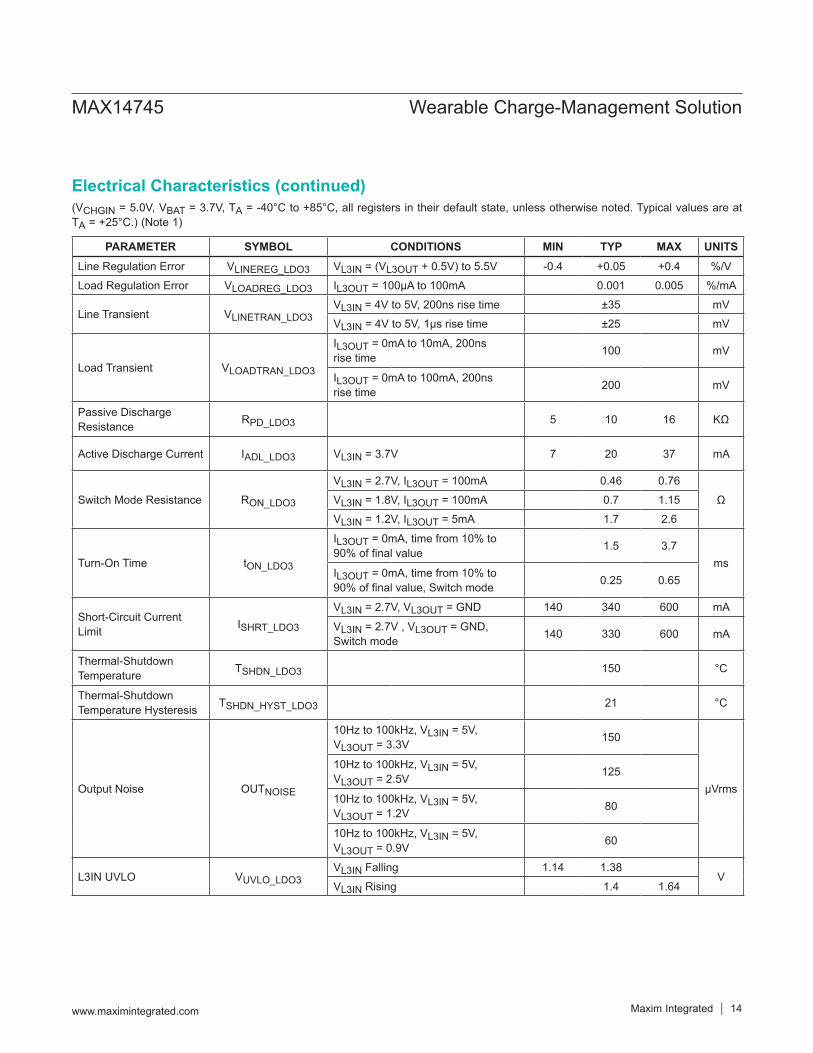
L2IN UVLO VUVLO_LDO2VL2IN Falling 1.14 1.38
VVL2IN Rising 1.4 1.64
LDO3(C = 1μF, unless otherwise noted. Typical values are at VL3IN = 3.7V, with IL3OUT = 10mA, VL3OUT = 3V.)
Input Voltage VINLDO3LDO mode 1.71 5.5 VSwitch mode 1.2 5.5 V
Quiescent Supply Current IQ_LDO3
IL3OUT = 0µA 1 5.1µA
IL3OUT = 0µA, Switch mode 0.5
Quiescent Supply Current in Dropout IQDO_LDO3
IL3OUT = 0µA, VL3IN = 2.9V, LDO3VSet = 3V. 1.8 µA
Shutdown Supply Current with Active Discharge Enabled
ISD_LDO3 LDO3 disabled. LDO3ActDSC=1. 54 µA
Maximum Output Current IL3OUT_MAX
VL3IN ≥ 2.7V 100 mAVL3IN = 1.8V or lower 50 mA
Output Voltage VL3OUT 0.9 4 V
Output Accuracy ACCLDO3VL3IN = (VL3OUT + 0.5V) or higher, IL3OUT = 100µA -2.7 +2.7 %
Dropout Voltage VDROP_LDO3VL3IN = 3V, IL3OUT_ = 100mA, LDO3VSet = 3V 100 mV
MAX14745 Wearable Charge-Management Solution
www.maximintegrated.com Maxim Integrated 13
Electrical Characteristics (continued)
(VCHGIN = 5.0V, VBAT = 3.7V, TA = -40°C to +85°C, all registers in their default state, unless otherwise noted. Typical values are at TA = +25°C.) (Note 1)
PARAMETER SYMBOL CONDITIONS MIN TYP MAX UNITSLine Regulation Error VLINEREG_LDO3 VL3IN = (VL3OUT + 0.5V) to 5.5V -0.4 +0.05 +0.4 %/VLoad Regulation Error VLOADREG_LDO3 IL3OUT = 100µA to 100mA 0.001 0.005 %/mA
Line Transient VLINETRAN_LDO3VL3IN = 4V to 5V, 200ns rise time ±35 mVVL3IN = 4V to 5V, 1µs rise time ±25 mV
Load Transient VLOADTRAN_LDO3
IL3OUT = 0mA to 10mA, 200ns rise time 100 mV
IL3OUT = 0mA to 100mA, 200ns rise time 200 mV
Passive Discharge Resistance RPD_LDO3 5 10 16 KΩ
Active Discharge Current IADL_LDO3 VL3IN = 3.7V 7 20 37 mA
Switch Mode Resistance RON_LDO3
VL3IN = 2.7V, IL3OUT = 100mA 0.46 0.76ΩVL3IN = 1.8V, IL3OUT = 100mA 0.7 1.15
VL3IN = 1.2V, IL3OUT = 5mA 1.7 2.6
Turn-On Time tON_LDO3
IL3OUT = 0mA, time from 10% to 90% of final value 1.5 3.7
msIL3OUT = 0mA, time from 10% to 90% of final value, Switch mode 0.25 0.65
Short-Circuit Current Limit ISHRT_LDO3
VL3IN = 2.7V, VL3OUT = GND 140 340 600 mA
VL3IN = 2.7V , VL3OUT = GND, Switch mode 140 330 600 mA
Thermal-Shutdown Temperature TSHDN_LDO3 150 °C
Thermal-Shutdown Temperature Hysteresis TSHDN_HYST_LDO3 21 °C
Output Noise OUTNOISE
10Hz to 100kHz, VL3IN = 5V, VL3OUT = 3.3V 150
µVrms
10Hz to 100kHz, VL3IN = 5V, VL3OUT = 2.5V 125
10Hz to 100kHz, VL3IN = 5V, VL3OUT = 1.2V 80
10Hz to 100kHz, VL3IN = 5V, VL3OUT = 0.9V 60
L3IN UVLO VUVLO_LDO3VL3IN Falling 1.14 1.38
VVL3IN Rising 1.4 1.64
MAX14745 Wearable Charge-Management Solution
www.maximintegrated.com Maxim Integrated 14
Electrical Characteristics (continued)

(VCHGIN = 5.0V, VBAT = 3.7V, TA = -40°C to +85°C, all registers in their default state, unless otherwise noted. Typical values are at TA = +25°C.) (Note 1)
PARAMETER SYMBOL CONDITIONS MIN TYP MAX UNITSCHGIN TO SYS PATH (VCHGIN = 5.0V, VSYS = VSYS_REG)
Allowed CHGIN Input Voltage Range VCHGIN_RNG -5.5 28 V
VCHGIN Detect Threshold VCHGIN_DET
Rising 3.8 3.9 4.1V
Falling 3.0 3.1 3.2
VCHGIN Overvoltage Threshold VCHGIN_OV Rising 7.2 7.5 7.8 V
VCHGIN Overvoltage Threshold Hysteresis VCHGIN_OV_HYS 200 mV
VCHGIN Valid Trip Point VCHGIN-SYS_TPVCHGIN – VSYS, Rising, VBAT = 4V +30 +145 +290 mV
VCHGIN Valid Trip Point Hysteresis VCHGIN-SYS_TP_HYS 275 mV
Input Limiter Current ILIM
ILimCntl[1:0] = 00 0
mAILimCntl[1:0] = 01 90 100ILimCntl[1:0] = 10 450 550ILimCntl[1:0] = 11 1000
Internal CAP Regulator VCAP VCHGIN = 5V 3.9 4.2 4.7 V
CHGIN-SYS Regulation Voltage VCHGIN-SYS VCHGIN = 4V, ISYS = 1mA 40 mV
CHGIN to SYS On-Resistance RCHGIN-SYS VCHGIN = 4.4V, ISYS = 500mA 370 660 mΩ
Thermal-Shutdown Temperature TCHGIN_SHDN (Note 3) +150 oC
Thermal-Shutdown Temperature Hysteresis TCHGIN_SHDN_HYS 30 oC
Input Current Soft-Start Time tSFST_LIM 1 ms
Internal Supply Switchover Threshold VCCINT_TH VCHGIN = VCAP rising, VBAT = 4.2V 2.5 2.8 3.0 V
MAX14745 Wearable Charge-Management Solution
www.maximintegrated.com Maxim Integrated 15
Electrical Characteristics (continued)

(VCHGIN = 5.0V, VBAT = 3.7V, TA = -40°C to +85°C, all registers in their default state, unless otherwise noted. Typical values are at TA = +25°C.) (Note 1)
PARAMETER SYMBOL CONDITIONS MIN TYP MAX UNITSSYS, BATTERY, AND VCCINT UVLOs
SYS UVLO ThresholdVSYSUVLO_R Rising 2.64 2.69 VVSYSUVLO_F Falling 2.57 2.62 2.67 V
SYS UVLO Threshold Hysteresis VSYSUVLO_HYS Hysteresis 26 mV
SYS UVLO Falling Debounce Time tSYSUVLO_FDEB SYS Falling 20 µs
VCCINT UVLO Threshold (POR) VUVLO VCCINT Rising 0.8 1.82 2.6 V
VCCINT UVLO Threshold Hysteresis VUVLO_HYS 140 mV
BAT UVLO Threshold VBAT_UVLO
Rising (Valid only when CHGIN is present. When VBAT < VBAT_UVLO, the BAT-SYS switch opens and BAT is connected to SYS through a diode.)
1.9 2.05 2.2 V
BAT UVLO Threshold Hysteresis VBAT_UVLO_HYS Hysteresis 50 mV
BATTERY CHARGER (See Figure 5a and Figure 5b)(VBAT = 4.2V. Typical values are at VCHGIN = 5.0V, VSYS = VSYS_REG)
Allowed BAT Voltage Range VBAT_RNG 0 5.5 V
BAT to SYS On-Resistance RBAT-SYS VBAT = 4.2V, IBAT = 300mA 80 140 mΩ
Current Reduce Thermal Threshold Temperature TCHG_LIM (Note 4) 120 oC
BAT-to-SYS Switch-On Threshold VBAT-SYS-ON SYS falling 10 22 35 mV
BAT-to-SYS Switch-Off Threshold VBAT-SYS-OFF SYS rising -3 -1.5 0 mV
SYS-BAT Regulation Voltage VSYS_REG VCHGIN = 5V, ISYS = 1mA VBatReg
+ 140mVVBatReg + 200mV
VBatReg + 260mV V
MAX14745 Wearable Charge-Management Solution
www.maximintegrated.com Maxim Integrated 16
Electrical Characteristics (continued)

(VCHGIN = 5.0V, VBAT = 3.7V, TA = -40°C to +85°C, all registers in their default state, unless otherwise noted. Typical values are at TA = +25°C.) (Note 1)
PARAMETER SYMBOL CONDITIONS MIN TYP MAX UNITS
SYS Threshold Voltage Charger Limiting Current (Note 5)
VSYS_LIM
SysMin = 000, VBAT > 3.6V VBAT+
0.1
V
SysMin = 000, VBAT < 3.4V 3.6
SysMin = 001, VBAT < 3.4V 3.7
SysMin = 010, VBAT < 3.4V 3.8
SysMin = 011, VBAT < 3.4V 3.9
SysMin = 100, VBAT < 3.4V 3.86 4 4.14
SysMin = 101, VBAT < 3.4V 4.1
SysMin = 110, VBAT < 3.4V 4.2
SysMin = 111, VBAT < 3.4V 4.3
Charger Current Soft-Start Time tCHG_SOFT 1 ms
PRECHARGE
Precharge Current IPCHG
IPChg = 00 5
%IFChgIPChg = 01 9 10 11IPChg = 10 20IPChg = 11 30
Prequalification Threshold VBAT_PChg
VPChg = 000 2.1
V
VPChg = 001 2.15 2.25 2.35VPChg = 010 2.40VPChg = 011 2.55VPChg = 100 2.7VPChg = 101 2.85VPChg = 110 3.0VPChg = 111 3.15
Prequalification Threshold Hysteresis VBAT_PChg_HYS 90 mV
MAX14745 Wearable Charge-Management Solution
www.maximintegrated.com Maxim Integrated 17
Electrical Characteristics (continued)
(VCHGIN = 5.0V, VBAT = 3.7V, TA = -40°C to +85°C, all registers in their default state, unless otherwise noted. Typical values are at TA = +25°C.) (Note 1)
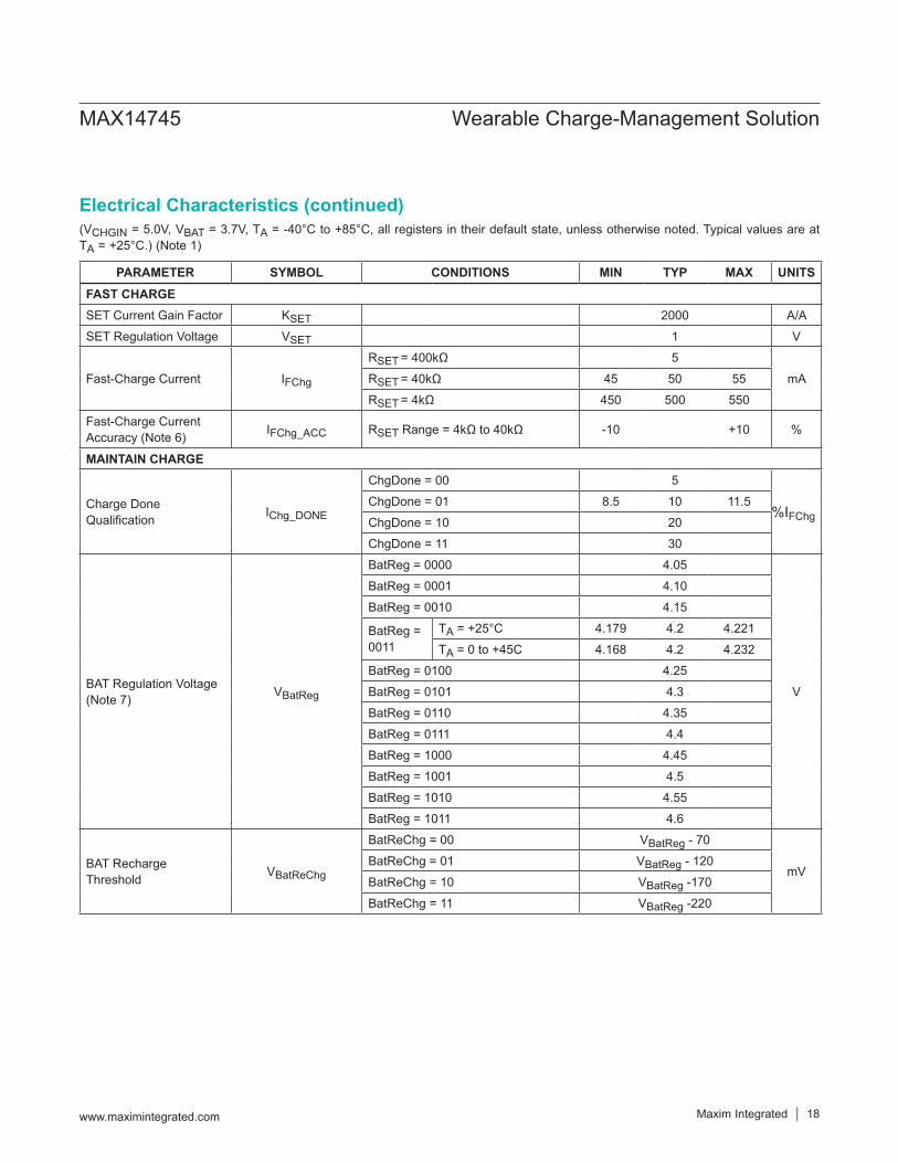
PARAMETER SYMBOL CONDITIONS MIN TYP MAX UNITSFAST CHARGESET Current Gain Factor KSET 2000 A/ASET Regulation Voltage VSET 1 V
Fast-Charge Current IFChg
RSET = 400kΩ 5mARSET = 40kΩ 45 50 55
RSET = 4kΩ 450 500 550
Fast-Charge Current Accuracy (Note 6) IFChg_ACC RSET Range = 4kΩ to 40kΩ -10 +10 %
MAINTAIN CHARGE
Charge DoneQualification IChg_DONE
ChgDone = 00 5
%IFChgChgDone = 01 8.5 10 11.5ChgDone = 10 20ChgDone = 11 30
BAT Regulation Voltage(Note 7) VBatReg
BatReg = 0000 4.05
V
BatReg = 0001 4.10BatReg = 0010 4.15
BatReg = 0011
TA = +25°C 4.179 4.2 4.221TA = 0 to +45C 4.168 4.2 4.232
BatReg = 0100 4.25BatReg = 0101 4.3BatReg = 0110 4.35BatReg = 0111 4.4BatReg = 1000 4.45BatReg = 1001 4.5BatReg = 1010 4.55BatReg = 1011 4.6
BAT Recharge Threshold VBatReChg
BatReChg = 00 VBatReg - 70
mVBatReChg = 01 VBatReg - 120BatReChg = 10 VBatReg -170BatReChg = 11 VBatReg -220
MAX14745 Wearable Charge-Management Solution
www.maximintegrated.com Maxim Integrated 18
Electrical Characteristics (continued)

(VCHGIN = 5.0V, VBAT = 3.7V, TA = -40°C to +85°C, all registers in their default state, unless otherwise noted. Typical values are at TA = +25°C.) (Note 1)
PARAMETER SYMBOL CONDITIONS MIN TYP MAX UNITSCHARGER TIMER
Maximum Prequalification Time tPChg
PChgTmr = 00 30
minPChgTmr = 01 60PChgTmr = 10 120PChgTmr = 11 240
Maximum Fast-Charge Time tFChg
FChgTmr = 00 75
minFChgTmr = 01 150FChgTmr = 10 300FChgTmr = 11 600
Maintain-Charge Time tTOChg
TOChgTmr = 00 0
minTOChgTmr = 01 15TOChgTmr = 10 30TOChgTmr = 11 60
Timer Accuracy tCHG_ACC -10 +10 %
Timer Extend Threshold TIMEXD_THRES
If charge current is reduced due to ILIM or TDIE this is the percentage of charge current below which timer clock operates at half speed
50 %IFChg
Timer Suspend Threshold TIMSUS_THRES
If charge current is reduced due to ILIM or TDIE this is the percentage of charge current below which timer clock pauses
20 %IFChg
THERMISTOR MONITOR AND NTC DETECTION
THM Hot Threshold T4
VTHM falling, MAX14745A/MAX14745C 30.9 32.9 34.9
%CAP
VTHM falling, MAX14745D/MAX14745E 21.3 23.3 25.3
THM Warm Threshold T3
VTHM falling, MAX14745A/ MAX14745C 48 50 52
VTHM falling, MAX14745D/ MAX14745E 30.9 32.9 34.9
THM Cool Threshold T2 VTHM rising 62.5 64.5 66.5THM Cold Threshold T1 VTHM rising 71.9 73.9 75.9THM Disable Threshold THMDIS VTHM rising 91 93 95
THM Threshold Hysteresis THMHYS 60 mV
THM Input Leakage ILKG_THM -1 1 µA
MAX14745 Wearable Charge-Management Solution
www.maximintegrated.com Maxim Integrated 19
Electrical Characteristics (continued)

(VCHGIN = 5.0V, VBAT = 3.7V, TA = -40°C to +85°C, all registers in their default state, unless otherwise noted. Typical values are at TA = +25°C.) (Note 1)
MAX14745 Wearable Charge-Management Solution
www.maximintegrated.com Maxim Integrated 20
PARAMETER SYMBOL CONDITIONS MIN TYP MAX UNITSSTART UP TIMING (See Figure 2)
Boot Delay tRST
BootDly = 00 80
msBootDly = 01 120BootDly = 10 220BootDly = 11 420
Boot Delay Timer Accuracy tRST_ACC -10 10 %
DIGITAL SIGNALS
Input Logic-High (SDA, SCL, MPC0, MPC1, PFN1, PFN2)
VIH 1.4 V
Input Logic-Low (SDA, SCL, MPC0, MPC1, PFN1, PFN2)
VIL 0.5 V
Output Logic-Low (SDA, RST, INT, LED, PFN2) VOL IOL = 4mA 0.4 V
High Level Leakage Current (SDA, RST, INT, LED, PFN2)
ILK 1 µA
SCL Clock Frequency fSCL 400 kHz
Bus Free Time Between a STOP and START Condition
tBUF 1.3 µs
START Condition (Repeated) Hold Time tHD:STA (Note 8) 0.6 µs
Low Period of SCL Clock tLOW 1.3 µs
High Period of SCL Clock tHIGH 0.6 µs
Setup Time for a Repeated START Condition
tSU:STA 0.6 µs
Data Hold Time tHD:DAT (Note 9) 0 0.9 µsData Setup Time tSU:DAT (Note 9) 100 ns
Setup Time for STOP Condition tSU:STO 0.6 µs
Spike Pulse Widths Suppressed by Input Filter
tSP (Note 10) 50 ns
Electrical Characteristics (continued)

Note 1: All devices are 100% production tested at TA = +25°C. Limits over the operating temperature range guaranteed by design.
Note 2: This value is included in the IBAT quiescent current values for the ON states.Note 3: When the die temperature exceeds TCHGIN_SHDN, the CHGIN to SYS path opens, and the charger is turned off.Note 4: When the die temperature exceeds TCHG_LIM, the charger current starts to decrease. Note 5: This is the threshold at which the charger starts to limit the current due to SYS dropping; if VSYS drops below this value
the charger will not move to maintain charge.Note 6: Fast charge current accuracy tested only at 50mA and 500mA, all other values guaranteed by design.Note 7: Values over temperature are not production tested and guaranteed by characterization.Note 8: fSCL must meet the minimum clock low time plus the rise/fall times.Note 9: The maximum tHD:DAT has to be met only if the device does not stretch the low period (tLOW) of the SCL signal.Note 10: Filters on SDA and SCL suppress noise spikes at the input buffers and delay the sampling instant.
(VCHGIN = 5.0V, VBAT = 3.7V, TA = -40°C to +85°C, all registers in their default state, unless otherwise noted. Typical values are at TA = +25°C.) (Note 1)
MAX14745 Wearable Charge-Management Solution
www.maximintegrated.com Maxim Integrated 21
Electrical Characteristics (continued)

(VBAT = 3.7V, VCHGIN = 0V, registers in their default state, TA = +25°C, unless otherwise noted.)
0
200
400
600
800
-40 -15 10 35 60 85
I CHGI
N(m
A)
TEMPERATURE (°C)
ICHGIN vs. TEMPERATUREtoc07
VBAT = 3.7VVCHGIN = 5VISYS = 600mA
ILimCntl[1:0] = 0x01
ILimCntl[1:0] = 0x02
0
10
20
30
40
50
60
70
80
90
100
0.001 0.01 0.1 1 10 100 1000
EFFI
CIEN
CY (%
)
IB2OUT (mA)
BUCK2 EFFICIENCY vs. LOADtoc8
VBAT = 3.7VVBAT = 3.3V
VBAT = 4.2V
VB2OUT = 1.8V
0
2
4
6
8
10
-40 -15 10 35 60 85
I BAT
(µA)
BAT
TERY
INPU
T CU
RREN
T
TEMPERATURE (°C)
IBAT vs. TEMPERATURE toc01
VBAT = 3.7V
POWER OFF
BUCKS ON, LDO1 ON
BUCKS ON
BUCKS ON, ALL LDOS ON
4.18
4.19
4.2
4.21
4.22
-40 -15 10 35 60 85
V BAT_
REG
(V)
TEMPERATURE (°C)
VBAT_REG vs. TEMPERATUREtoc04
VCHGIN = 5VBatReg[2:0] = 011RSET = 40kΩ4.2kΩ at BAT
0
2
4
6
8
10
2.7 3 3.3 3.6 3.9 4.2
I BAT
(µA)
BAT
TERY
INPU
T CU
RREN
T
VBAT (V)
IBAT vs. VBAT toc02
POWER OFF
BUCKS ON, ALL LDOS ON
BUCKS ON, LDO1 ON
BUCKS ON
0
1
2
3
4
5
6
0
40
80
120
160
200
0 40 80 120 160 200 240 280
V BAT
(V)
I BAT
(mA)
TIME (minutes)
IBAT/VBAT vs. TIME toc05
VBAT
IBAT
150mAhr BATTERY IChgDone[1:0 ]= 01IPChg[1:0 = 01VPChg[2:0] = 110RSET = 40kΩ
0
20
40
60
80
100
-40 -15 10 35 60 85
I FCHG
(mA)
TEMPERATURE (°C)
IFCHG vs. TEMPERATUREtoc03
VCHGIN = 5VRSET = 40kΩIPChg[1:0] = 01
VBAT = 2V
VBAT = 3.7V
0.0
1.0
2.0
3.0
4.0
5.0
6.0
3 4 5 6 7 8
V SYS
(V)
VCHGIN (V)
VSYS vs. VCHGIN toc06
VBAT = 2.8VRSYS = 50Ω
MAX14745 Wearable Charge-Management Solution
Maxim Integrated 22www.maximintegrated.com
Typical Operating Characteristics

(VBAT = 3.7V, VCHGIN = 0V, registers in their default state, TA = +25°C, unless otherwise noted.)
2.9
2.95
3
3.05
3.1
0 20 40 60 80 100
V L2OU
T(V
)
IL2OUT (mA)
VL2OUT vs. LOADtoc15
VBAT = 3.3V, 3.7V, 4.2V
VL2OUT = 3.0V
1.7
1.74
1.78
1.82
1.86
1.9
0 100 200 300 400
V B2OU
T(V
)
IB1OUT (mA)
VB2OUT vs. LOADtoc9
VBAT = 3.3V, 3.7V, 4.2V
VB2OUT = 1.8V
50mA/div
toc12
20µs/div
BUCK1 TRANSIENT RESPONSE
VB1OUT 20mV/div
IB1OUT
VB1OUT = 1.2V
0
10
20
30
40
50
60
70
80
90
100
0.001 0.01 0.1 1 10 100 1000
EFFI
CIEN
CY (%
)
IB1OUT (mA)
BUCK1 EFFICIENCY vs. LOADtoc10
VBAT = 3.7V
VBAT = 3.3V
VBAT = 4.2V
VB1OUT = 1.2V
50mA/div
toc13
20µs/div
BUCK2 TRANSIENT RESPONSE
VB2OUT 20mV/div
IB2OUT
VB2OUT = 1.8V
2.9
2.95
3
3.05
3.1
0 20 40 60 80 100
V L3OU
T(V
)
IL3OUT (mA)
VL3OUT vs. LOADtoc16
VBAT = 3.3V, 3.7V, 4.2V
VL3OUT = 3.0V
1
1.05
1.1
1.15
1.2
1.25
1.3
0 100 200 300 400
V B1OU
T(V
)
IB1OUT (mA)
VB1OUT vs. LOAD toc11
VBAT = 3.3V, 3.7V, 4.2V
VBAT = 3.3V, 3.7V, 4.2V
VB1OUT = 1.2V
2.9
2.95
3
3.05
3.1
0 20 40 60 80 100
V L1OU
T(V
)
IL1OUT (mA)
VL1OUT vs. LOAD toc14
VBAT = 3.3V, 3.7V, 4.2V
VL1OUT = 3.0V
50mA/div
toc17
100ms/div
LDO1 TRANSIENT RESPONSE
VOUT 200mV/div
IOUT
VL1OUT = 3.0V
MAX14745 Wearable Charge-Management Solution
Maxim Integrated 23www.maximintegrated.com
Typical Operating Characteristics (continued)

(VBAT = 3.7V, VCHGIN = 0V, registers in their default state, TA = +25°C, unless otherwise noted.)
50mA/div
toc18
40µs/div
LDO1 TRANSIENT RESPONSE
VOUT 200mV/div
IOUT
VL1OUT = 3.0V
50mA/div
toc19
100ms/div
LDO2 TRANSIENT RESPONSE
VOUT 200mV/div
IOUT
VL2OUT = 3.0V
50mA/div
toc20
40µs/div
LDO2 TRANSIENT RESPONSE
VOUT 200mV/div
IOUT
VL2OUT = 3.0V
Typical Operating Characteristics (continued)
50mA/div
toc21
100ms/div
LDO3 TRANSIENT RESPONSE
VOUT 200mV/div
IOUT
VL3OUT = 3.0V
50mA/div
toc22
40µs/div
LDO3 TRANSIENT RESPONSE
VOUT 200mV/div
IOUT
VL3OUT = 3.0V
MAX14745 Wearable Charge-Management Solution
Maxim Integrated 24www.maximintegrated.com

BUMP NAME FUNCTION
A1 L1OUT LDO1 Output. Bypass with a minimum 1µF capacitor to GND.
A2 L1IN LDO1 Input
A3 CAP Bypass for Internal LDO. Bypass with a 1µF capacitor to GND.
A4, C3, C4 D3, D4, F4 GND Ground
A5 B2OUT 0.8V – 3.95V Buck Regulator Output Feedback. Bypass with a 10µF capacitor to GND.
A6 B2LX 0.8V – 3.95V Buck Regulator Switch. Connect 2.2µH inductor to B2OUT.
B1 L2OUT LDO2 Output. Bypass with a minimum 1µF capacitor to GND.
B2 L2IN LDO2 Input
B3 INT Open-Drain, Active-Low Interrupt Output.
B4 MON Voltage Monitor Pin
B5,B6 BAT Battery Connection. Connect BAT to a positive battery terminal, bypass BAT with a minimum 1µF capacitor to GND.
MAX14745 Wearable Charge-Management Solution
www.maximintegrated.com Maxim Integrated 25
Bump Configuration
Bump Description
MAX14745TOP VIEW
(BUMP SIDE DOWN)
A
B
C
D
WLP(2.72mm x 2.47mm)
E
F
1+
L1OUT L1IN CAP GND B2OUT B2LX
2 3 4 5 6
L2OUT L2IN INT MON BAT BAT
L3OUT L3IN GND GND SET SYS
LED PFN2 GND GND EXT SYS
RST MPC0 MPC1 PFN1 CHGIIN CHGIN
SDA SCL THM GND B1OUT B1LX

Note: All capacitance values listed in this document refer to effective capacitance. Be sure to specify capacitors that will meet these requirements under typical system operating conditions taking into consideration the effects of voltage and temperature.
PIN NAME FUNCTION
C1 L3OUT LDO3 Output. Bypass with a minimum 1µF capacitor to GND.
C2 L3IN LDO3 Input
C5 SET External Resistor For Battery Charge Current Level Setting. Do not connect any external capacitance on this pin; maximum allowed capacitance (CSET < 5µs/RSET) pF.
C6, D6 SYS System Load Connection. Connect SYS to the system load. Bypass SYS with a minimum 10µF low-ESR ceramic capacitor to GND.
D1 LED LED Open-Drain Pulldown Current. Add an external current limiting pullup resistor.
D2 PFN2 Power Function Control Input/Output. Programmable functionality via PwrFnMode. See Table 1.
D5 EXTPush-Pull Gate Drive for Optional External pFET from BAT-to-SYS. Output is pulled to GND when charger is disconnected and internal BAT-SYS FET is switched on. Otherwise, this output is pulled high to the SYS voltage.
E1 RST Power-On Reset Output. Active-low, open-drain.
E2 MPC0 Multipurpose Configuration Input 0
E3 MPC1 Multipurpose Configuration Input 1
E4 PFN1 Power Function Control Input. Programmable functionality via PwrFnMode. See Table 1.
E5, E6 CHGIN -5.5V/+28V Protected Charger Input. Bypass CHGIN with 1µF capacitor to GND.
F1 SDA Open-Drain, I2C Serial Data Input/Output.
F2 SCL I2C Serial Clock Input
F3 THM Battery Temperature Thermistor Measurement Connection. Connect a 10kΩ resistor from THM to CAP and a 10kΩ, 3380A NTC thermistor from THM to GND.
F5 B1OUT 0.8V – 2.375V Buck Regulator Output Feedback. Bypass B1OUT with a 10µF capacitor to GND.
F6 B1LX 0.8V – 2.375V Buck Regulator Switch Terminal. Connect B1LX to B1OUT with a 2.2µH inductor.
MAX14745 Wearable Charge-Management Solution
www.maximintegrated.com Maxim Integrated 26
Bump Description (continued)
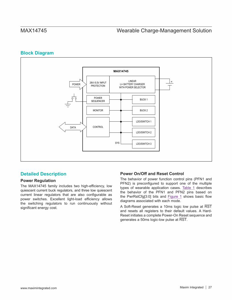
Detailed DescriptionPower RegulationThe MAX14745 family includes two high-efficiency, low quiescent current buck regulators, and three low quiescent current linear regulators that are also configurable as power switches. Excellent light-load efficiency allows the switching regulators to run continuously without significant energy cost.
Power On/Off and Reset ControlThe behavior of power function control pins (PFN1 and PFN2) is preconfigured to support one of the multiple types of wearable application cases. Table 1 describes the behavior of the PFN1 and PFN2 pins based on the PwrRstCfg[3:0] bits and Figure 1 shows basic flow diagrams associated with each mode.A Soft-Reset generates a 10ms logic low pulse at RST and resets all registers to their default values. A Hard-Reset initiates a complete Power-On Reset sequence and generates a 50ms logic-low pulse at RST.
MAX14745 Wearable Charge-Management Solution
www.maximintegrated.com Maxim Integrated 27
Block Diagram
MAX14745
SYS
LINEARLi+ BATTERY CHARGER
WITH POWER SELECTOR
28V/-5.5V INPUT PROTECTION
POWERSEQUENCER BUCK 1
MONITOR BUCK 2
CONTROL
LDO/SWITCH 1
LDO/SWITCH 2
LDO/SWITCH 3
POWER
DATA
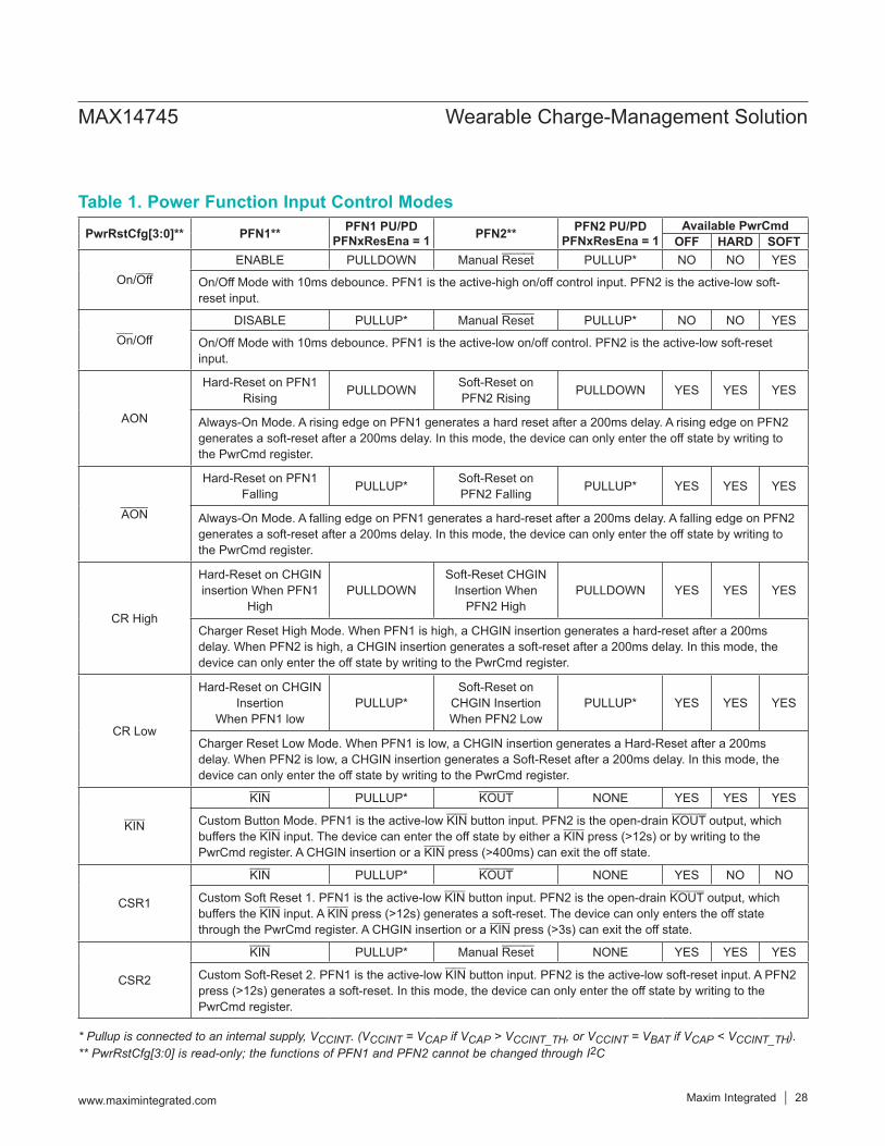
Table 1. Power Function Input Control Modes
* Pullup is connected to an internal supply, VCCINT. (VCCINT = VCAP if VCAP > VCCINT_TH, or VCCINT = VBAT if VCAP < VCCINT_TH).** PwrRstCfg[3:0] is read-only; the functions of PFN1 and PFN2 cannot be changed through I2C
PwrRstCfg[3:0]** PFN1** PFN1 PU/PD PFNxResEna = 1 PFN2** PFN2 PU/PD
PFNxResEna = 1 Available PwrCmd
OFF HARD SOFT
On/Off ENABLE PULLDOWN Manual Reset PULLUP* NO NO YES
On/Off Mode with 10ms debounce. PFN1 is the active-high on/off control input. PFN2 is the active-low soft-reset input.
On/OffDISABLE PULLUP* Manual Reset PULLUP* NO NO YES
On/Off Mode with 10ms debounce. PFN1 is the active-low on/off control. PFN2 is the active-low soft-reset input.
AON
Hard-Reset on PFN1 Rising PULLDOWN Soft-Reset on
PFN2 Rising PULLDOWN YES YES YES
Always-On Mode. A rising edge on PFN1 generates a hard reset after a 200ms delay. A rising edge on PFN2 generates a soft-reset after a 200ms delay. In this mode, the device can only enter the off state by writing to the PwrCmd register.
AON
Hard-Reset on PFN1 Falling PULLUP* Soft-Reset on
PFN2 Falling PULLUP* YES YES YES
Always-On Mode. A falling edge on PFN1 generates a hard-reset after a 200ms delay. A falling edge on PFN2 generates a soft-reset after a 200ms delay. In this mode, the device can only enter the off state by writing to the PwrCmd register.
CR High
Hard-Reset on CHGIN insertion When PFN1
High PULLDOWN
Soft-Reset CHGIN Insertion When
PFN2 High PULLDOWN YES YES YES
Charger Reset High Mode. When PFN1 is high, a CHGIN insertion generates a hard-reset after a 200ms delay. When PFN2 is high, a CHGIN insertion generates a soft-reset after a 200ms delay. In this mode, the device can only enter the off state by writing to the PwrCmd register.
CR Low
Hard-Reset on CHGIN Insertion
When PFN1 low PULLUP*
Soft-Reset on CHGIN Insertion When PFN2 Low
PULLUP* YES YES YES
Charger Reset Low Mode. When PFN1 is low, a CHGIN insertion generates a Hard-Reset after a 200ms delay. When PFN2 is low, a CHGIN insertion generates a Soft-Reset after a 200ms delay. In this mode, the device can only enter the off state by writing to the PwrCmd register.
KIN
KIN PULLUP* KOUT NONE YES YES YES
Custom Button Mode. PFN1 is the active-low KIN button input. PFN2 is the open-drain KOUT output, which buffers the KIN input. The device can enter the off state by either a KIN press (>12s) or by writing to the PwrCmd register. A CHGIN insertion or a KIN press (>400ms) can exit the off state.
CSR1
KIN PULLUP* KOUT NONE YES NO NO
Custom Soft Reset 1. PFN1 is the active-low KIN button input. PFN2 is the open-drain KOUT output, which buffers the KIN input. A KIN press (>12s) generates a soft-reset. The device can only enters the off state through the PwrCmd register. A CHGIN insertion or a KIN press (>3s) can exit the off state.
CSR2
KIN PULLUP* Manual Reset NONE YES YES YES
Custom Soft-Reset 2. PFN1 is the active-low KIN button input. PFN2 is the active-low soft-reset input. A PFN2 press (>12s) generates a soft-reset. In this mode, the device can only enter the off state by writing to the PwrCmd register.
MAX14745 Wearable Charge-Management Solution
www.maximintegrated.com Maxim Integrated 28

Figure 1. Power Function Input Control Modes Flow Diagrams
MAX14745 Wearable Charge-Management Solution
www.maximintegrated.com Maxim Integrated 29

Power SequencingThere are multiple configuration options for the sequenc-ing of the buck regulators and LDOs during power-on. See Table 1 for details. Regulators can be configured to turn on at one of the four points during the power-on process: 0% tRST, 25% tRST, 50% tRST, and 100% tRST. The reset delay tRST can be set to 80ms, 120ms, 220ms, or 420ms by BootDly[1:0] in the BootCfg register. The power-on sequencing is depicted in Figure 2a and Figure 2b.Additionally, the regulators can be selected to default off and can be turned on with an I2C command after RST is released. Each LDO regulator can be configured to be always-on as long as SYS or BAT is present.
In general, if an undervoltage condition is detected on SYS the device goes into the off state. However if there is a valid voltage on CHGIN the behavior is determined by the ChgAlwTry setting. If ChgAlwTry = 0, and an undervoltage condition is detected on SYS during the sequencing process the device turns SYS and all other external resources off and waits for CHGIN removal. On CHGIN removal the device enters the off state to avoid draining the battery. If ChgAlwTry = 1, the process will continually recheck the SYS undervoltage condition every 500ms until it is no longer vaild before continuing with the sequencing process.
Figure 2a. Power-On Sequencing
MAX14745 Wearable Charge-Management Solution
www.maximintegrated.com Maxim Integrated 30
001 010
SYS
POR
RST
15ms
011 100 111
tRST
BUCK CANNOT BE ALWAYS ON
30ms 5ms30ms 15ms
CHGIN INSERTION OR KIN PRESS*
LDO_En
Buck_En**
CHGIN INSERTIONKIN PRESS
_Seq0% 25% 50% 100%% OF tRST ALWAYS-ON
*KIN PRESS TURN-ON ENABLED VIA SPECIFIC PwrRstCfg ONLY
**AFTER BEING ENABLED, THE BUCK CONVERTERS HAVE AN 8ms (TYP) BLANKING TIME BEFORE THE OUTPUT VOLTAGE STARTS TO RISE.
ENABLE VIA I2C/MPC
ENABLE VIA I2C/MPC

Smart Power SelectorThe smart power selector seamlessly distributes power from the external CHGIN input to the battery (BAT) and the system (SYS). With both an external adapter and battery connected, the smart power selector basic functions are:
When the system load requirements are less than the input current limit, the battery is charged with residual power from the input.
When the system load requirements exceed the input current limit, the battery supplies supplemental current to the load.
When the battery is connected and there is no external power input, the system is powered from the battery.
Thermal Current RegulationIn case the die temperature exceeds the normal limit, the MAX14745 will attempt to limit the temperature increase by reducing the input current from CHGIN. In this condi-tion, the system load has priority over charger current, so the input current is first reduced by lowering the charge current. If the junction temperature continues to rise and reaches the maximum operating limit, no input current is drawn from CHGIN and the battery powers the entire system load.
Figure 2b. Power-On Sequencing Without Battery
MAX14745 Wearable Charge-Management Solution
www.maximintegrated.com Maxim Integrated 31
001 010
SYS
POR
RST
011 100 111
tRST
BUCK CANNOTBE ALWAYS ON
CHGIN
LDO_En
Buck_En*
_Seq
0% 25% 50% 100%% of tRST ALWAYS
*After being enabled, the buck converters have an 8ms (typ) blanking time before the output voltage starts to rise.
-ON
15ms
30ms 15ms
ENABLE VIAI2C/MPC
ENABLE VIAI2C/MPC
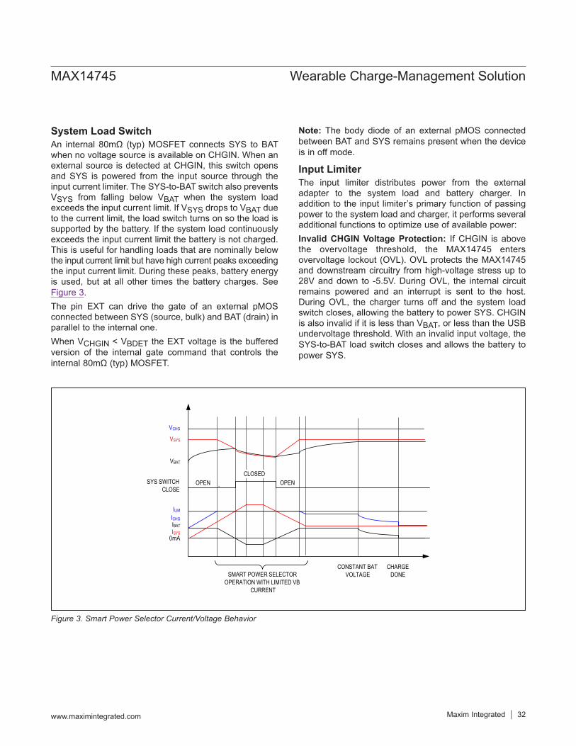
System Load SwitchAn internal 80mΩ (typ) MOSFET connects SYS to BAT when no voltage source is available on CHGIN. When an external source is detected at CHGIN, this switch opens and SYS is powered from the input source through the input current limiter. The SYS-to-BAT switch also prevents VSYS from falling below VBAT when the system load exceeds the input current limit. If VSYS drops to VBAT due to the current limit, the load switch turns on so the load is supported by the battery. If the system load continuously exceeds the input current limit the battery is not charged. This is useful for handling loads that are nominally below the input current limit but have high current peaks exceeding the input current limit. During these peaks, battery energy is used, but at all other times the battery charges. See Figure 3.The pin EXT can drive the gate of an external pMOS connected between SYS (source, bulk) and BAT (drain) in parallel to the internal one.When VCHGIN < VBDET the EXT voltage is the buffered version of the internal gate command that controls the internal 80mΩ (typ) MOSFET.
Note: The body diode of an external pMOS connected between BAT and SYS remains present when the device is in off mode.
Input LimiterThe input limiter distributes power from the external adapter to the system load and battery charger. In addition to the input limiter’s primary function of passing power to the system load and charger, it performs several additional functions to optimize use of available power:Invalid CHGIN Voltage Protection: If CHGIN is above the overvoltage threshold, the MAX14745 enters overvoltage lockout (OVL). OVL protects the MAX14745 and downstream circuitry from high-voltage stress up to 28V and down to -5.5V. During OVL, the internal circuit remains powered and an interrupt is sent to the host. During OVL, the charger turns off and the system load switch closes, allowing the battery to power SYS. CHGIN is also invalid if it is less than VBAT, or less than the USB undervoltage threshold. With an invalid input voltage, the SYS-to-BAT load switch closes and allows the battery to power SYS.
Figure 3. Smart Power Selector Current/Voltage Behavior
MAX14745 Wearable Charge-Management Solution
www.maximintegrated.com Maxim Integrated 32
ISYS
`
VCHG
VSYS
VBAT
ICHGIBAT
0mA
ILIM
SYS SWITCHCLOSE
OPEN
SMART POWER SELECTOROPERATION WITH LIMITED VB
CURRENT
OPENCLOSED
CONSTANT BATVOLTAGE
CHARGEDONE

CHGIN Adaptive Input Current Limit: The CHGIN input current is limited to prevent input overload. The input current limit is controlled by I2C. However, if the voltage at CHGIN collapses because the source is not able to supply either the current programmed in I2C, or the total current required by the battery charger and system load, the input current limit will be adaptively reduced.Thermal Limiting: In case the die temperature exceeds the normal limit (TCHG_LIM), the MAX14745 attempts to limit temperature increase by reducing the input current from CHGIN. In this condition, the system load has prior-ity over the charger current, so the input current is first reduced by lowering the charge current. If the junction temperature continues to rise and reaches the maximum operating limit (TCHGIN_SHDN), no input current is drawn from CHGIN and the battery powers the entire system load.Adaptive Battery Charging: While the system is powered from CHGIN, the charger draws power from SYS to charge the battery. If the total load exceeds the input current limit, an adaptive charger control loop reduces charge current to prevent VSYS from collapsing.When the charge current is reduced below 50% due to ILIM or TDIE, the timer clock operates at half speed. When the charge current is reduced below 20% due to ILIM or TDIE, the timer clock is paused.
Fast-Charge Current SettingThe MAX14745 uses an external resistor connected from SET to GND to set the fast-charge current. The pre-charge and charge-termination currents are programmed as a percentage of this value through I2C registers. The fast-charge current resistor can be calculated as:
RSET = KSET x VSET/IFChgwhere KSET has a typical value of 2000A/A and VSET has a typical value of 1V. The range of acceptable resistors for RSET is 4kΩ to 400kΩ
Thermistor Monitoring with Charger ShutdownThe MAX14745 features three modes for controlling charger behavior based on battery-pack temperature: Thermistor Monitoring, JEITA Monitoring 1, and JEITA Monitoring 2. The divider formed by a pull-up resistor (RPU) to CAP, optional parallel resistor (RPA) from THM to ground, and NTC thermistor (RTHM) from THM to ground, provides a voltage at THM that is proportional to temperature as a fraction of the CAP voltage. Two sets of preconfigured default thresholds (0°C/10°C/45°C/60°C or 0°C/10°C/25°C/45°C as a %CAP) optimized for beta 3380 thermistors are available (see Table 38). The four default thresholds create five temperature zones, and the fractional CAP voltage measured at the THM pin is compared to the thresholds to determine the active temperature zone during operation.The behavior in each temperature zone is determined by the configuration of bits in the I2C registers. The active monitoring mode is selected by ThermEn[1:0] in the ThrmCfrg register. In all modes, the T2IFchg[2:0] and T2T3IFchg[2:0], and T3T4IFchg[2:0] fields in the ThrmCfg registers set the fast charge current in three tempera-ture zones, T1_T2, T2_T3, and T3_T4. In Thermistor Monitoring mode, charging is enabled only in T1_T2 and T2_T3 and the battery termination voltage is equal to VBATREG, as shown in Figure 4a. In both JEITA Monitoring 1 and JEITA Monitoring 2 the charger is active in the T1_T2, T2_T3, and T3_T4 zones. However, JEITA Monitoring 1 sets the battery termination voltage to VBATREG for all zones, while JEITA Monitoring 2 sets the battery termination voltage to VBATREG - 150mV for zones T1_2 and T3_T4, as shown in Figure 4b. The behavior of all three modes is summarized in Table 2.
MAX14745 Wearable Charge-Management Solution
www.maximintegrated.com Maxim Integrated 33

Figure 4a. Charging Behavior Using Thermistor Monitoring Mode
Figure 4b. Charging Behavior Using JEITA Monitoring 1 and 2 Modes
MAX14745 Wearable Charge-Management Solution
www.maximintegrated.com Maxim Integrated 34
T1 T4
TEMPERATURE (°C)
CHARGINGNO CHARGING NO CHARGING
T2 T3
IPCHG
PREQUAL:VBAT<VBAT_PCHG
T1 T4
TEMPERATURE (°C)
CHARGINGNO CHARGING NO CHARGING
T2 T3
IFCHG_T1-T2
FAST CHARGE CONSTANT CURRENT:VBAT_PCHG < VBAT < VBAT_REG
IFCHG_T2-T3
T1 T4
TEMPERATURE (°C)
CHARGINGNO CHARGING
T2 T3
VBATREG
REGULATED VOLTAGE
RTHM RPA
RPU
CAP
NO CHARGING
T1 T4
TEMPERATURE (°C)
CHARGINGNO CHARGING
NO CHARGING
T2 T3
T1 T4
TEMPERATURE (°C)
CHARGINGNO
CHARGINGNO
CHARGING
T2 T3
IPCHG
VBATREG-150mV-150mV
PREQUAL:VBAT<VBAT_PCHG(BOTH MODES)
T1 T4
TEMPERATURE (°C)
CHARGINGNO CHARGING
NO CHARGING
T2 T3
IFCHG_T1-T2
FAST-CHARGE CONSTANT-CURRENT:VBAT_PCHG < VBAT < VBAT_REG
(BOTH MODES)
IFCHG_T2-T3 IFCHG_T3-T4
T1 T4
TEMPERATURE (°C)
CHARGINGNO
CHARGINGNO
CHARGING
T2 T3
VBATREG
REGULATED VOLTAGE(JEITA MONITORING 2)
REGULATED VOLTAGE(JEITA MONITORING 1)

I2C InterfaceThe device uses the two-wire I2C interface to communicate with the host microcontroller. The configuration settings and status information provided through this interface are detailed in the register descriptions.
I2C AddressesThe registers of the MAX14745 are accessed through the slave address of 0101000 (0x50 for writes/0x51 for reads).
Table 2. Thermistor Monitoring/JEITA Monitoring Enable Control
ThermEn[1:0] DESCRIPTIONCHARGER MODE
T < T1 T1 < T < T2 T2 < T < T3 T3 < T < T4 T >T4
00Thermistor/
JEITA Monitoring OFF
As per I2C settings
01 Thermistor Monitoring ON OFF
IPCHG = IPChg,IFChg = T1T2IFchg,Regulated Voltage =
VBATREG
IPCHG = IPChg,IFChg = T2T3IFchg,Regulated Voltage =
VBATREG
OFF OFF
10 JEITA Monitoring 1 ON OFF
IPCHG = IPChg,IFChg = T1T2IFchg,Regulated Voltage =
VBATREG
IPCHG = IPChg,IFChg = T2T3IFchg
Regulated Voltage = VBATREG
IPCHG = IPChg,IFChg = T3T4IFchg
Regulated Voltage = VBATREG
OFF
11 JEITA Monitoring 2 ON OFF
IPCHG = IPChg,IFChg = T1T2IFchg,Regulated Voltage = VBATREG - 150mV
IPCHG = IPChg, IFChg = T2T3IFchg,Regulated Voltage =
VBATREG
IPCHG = IPChg,IFChg = T3T4IFchg,Regulated Voltage = VBATREG - 150mV
OFF
MAX14745 Wearable Charge-Management Solution
www.maximintegrated.com Maxim Integrated 35

Thermistor Monitoring with Charger Shutdown
Figure 5a. Charger State Diagram (Thermistor Monitoring with Charger Shutdown)
MAX14745 Wearable Charge-Management Solution
www.maximintegrated.com Maxim Integrated 36
MAINTAINCHARGE DONE
ChgStat = 110LED = OFF
ICHG = 0
CHARGER OFF
ChgStat = 000LED = OFF
ICHG = 0
PREQUAL
ChgStat = 010LED = ON
ICHG = IPCHG
FAST CHARGE
(CONSTANT CURRENT)ChgStat = 011
ICHG = IFCHG**LED = ON
FAST CHARGE
(CONSTANT VOLTAGE)ChgStat = 100
LED = ONICHG = IFCHG
MAINTAINCHARGE
ChgStat = 101LED = ON
ICHG < ICHG_DONE
CHARGE SUSPEND
ChgStat = 001LED = 1.5s PERIOD
ICHG = 0
FAULT
ChgStat = 111LED = 0.15s PERIOD
ICHG = 0
PREQUAL SUSPEND
ChgStat = 001LED = 1.5s PERIOD
ICHG = 0
FAST CHARGE
CC SUSPENDChgStat = 001
LED = 1.5s PERIODICHG = 0
FAST CHARGE
CV SUSPEND
ChgStat = 001LED = 1.5s PERIOD
ICHG = 0
ChgEn = 1, VSYS > VSYS_LIM
VBAT > VBAT_PChgRESET CHARGE TIMER
VBAT < VBAT_PChgRESET CHARGE TIMER
VOLTAGE MODE = 1* AND VSYS > VSYS_LIM
(VOLTAGE MODE = 0*AND VSYS > VSYS_LIM)OR VBAT < VBAT_PChg
RECOVER FROM FAULTRESET CHARGE TIMER
T1 < T < T3
T < T1 or T > T3
T1<T<T3
T<T1 or T>T3
T1<T<T3
T<T1 or T>T3
RESET CHARGE TIMERT1 < T < T4
T < T1 or T > T3
T < T1 or T > T3
ICHG > ICHG_DONE ChgAutoStp = 0"
RESET CHARGE TIMER
ICHG < ICHG_DONE AND
VSYS > VSYS_LIMAND
TDIE < TCHG_LIMRESET CHARGE TIMER
tCHG_TIMER > tMTCHGAND
ChgAutoStp = 1
VBAT < VBATREG – VBATREAND ChgAutoReSta = 1AND VSYS > VSYS_LIM
RESET CHARGE TIMER
PAUSE CHARGE
TIMER
PAUSE CHARGE
TIMER
tCHG_TIMER > tPCHG
tCHG_TIMER > tFCHG
TDIE < TBUS_LIMOR VBAT > VSYSOR ChgEn = 0
FROM ANY STATE
NOTES:* VOLTAGE MODE IS AN INTERNAL SIGNAL
** CHARGE TIMER IS SLOWED BY 50% IF ICHG < IFCHG / 2 AND PAUSED IF ICHG < IFCHG/5 ONLY IN FAST CHARGE CONSTANT CURRENT STATE
tMTCHG
PAUSE CHARGE
TIMER

Figure 5b. Battery Charger State Diagram (JEITA Monitoring with Charger Shutdown)
MAX14745 Wearable Charge-Management Solution
www.maximintegrated.com Maxim Integrated 37
MAINTAINCHARGE DONE
ChgStat=110LED=OFF
ICHG=0
CHARGER OFF
ChgStat=000LED=OFF
ICHG=0
PREQUAL
ChgStat=010LED=ON
ICHG=IPCHG
FAST CHARGE
(CONSTANT CURRENT)ChgStat=011
LED=ONICHG=IFCHG**
FAST CHARGE
(CONSTANT VOLTAGE)ChgStat=100
LED=ONICHG=IFCHG
MAINTAINCHARGE
ChgStat=101LED=ON
ICHG<ICHG_DONE
FRESH BATTERY INSERTION
ChgStat=110LED=1s pulse
ICHG=0
CHARGE SUSPENDChgStat=001
LED=1.5s periodICHG=0
FAULTChgStat=111
LED=0.15s PERIODICHG=0
PREQUAL SUSPEND
ChgStat=001LED=1.5s PERIOD
ICHG=0
FAST CHARGE
CC SUSPEND
ChgStat=001LED=1.5s PERIOD
ICHG=0
FAST CHARGE
CV SUSPENDChgStat=001
LED=1.5s PERIODICHG=0
ChgEn=1AND
VSYS>VSYS_LIM
VBAT>VBAT_PChgRESET CHARGE TIMER
VBAT<VBAT_PChgRESET CHARGE TIMER
VOLTAGE MODE=1*AND
VSYS>VSYS_LIM
(VOLTAGE MODE=0*AND VSYS>VSYS_LIM)OR VBAT<VBAT_PChg
RECOVER FROM FAULTRESET CHARGE TIMER
T1<T<T4
T<T1 or T>T4
T1<T<T4
T<T1 or T>T4
T1<T<T4
T<T1 or T>T4
RESET CHARGE TIMERT1<T<T4
T<T1 or T>T4
T<T1 or T>T4
T<T1 or T>T4
ChgEn=1,VBAT > VBATREG – VBATRECHG
ChgEn=1,VBAT>VBATREG–VBATRECHG
Freshbat_dis=0
ICHG>ICHG_DONE ChgAutoStp=0"
RESET CHARGE TIMER
ICHG<ICHG_DONE AND
VSYS>VSYS_LIMAND
TDIE<TCHG_LIMRESET CHARGE TIMER
tCHG_TIMER>tMTCHGAND
ChgAutoStp=1
VBAT<VBATREG–VBATRECHGand ChgAutoReSta=1And VSYS>VSYS_LIM
RESET CHARGE TIMER
PAUSE CHARGE
TIMER
PAUSE CHARGE
TIMER
PAUSE CHARGE
TIMER
tCHG_TIMER>tPCHG
tCHG_TIMER>tFCHG
TDIE<TBUS_LIMor VBAT>VSYSor ChgEn=0
FROM ANY STATE
NOTES:* VOLTAGE MODE IS AN INTERNAL SIGNAL
** CHARGE TIMER IS SLOWED BY 50% IF ICHG < IFCHG/2 AND PAUSED IF ICHG < IFCHG/5 ONLY IN FAST CHARGE CONSTANT CURRENT STATE WHERE IFCHG IS THE EFFECTIVE FAST CHARGE CURRENT INCLUDING JEITA CURRENT LIMITATION
T<T2 or T>T3
VBAT<VBATREG–VBATRECHG
1s
tMTCHG

I2C InterfaceThe MAX14745 contain an I2C-compatible interface for data communication with a host controller (SCL and SDA). The interface supports a clock frequency of up to 400kHz. SCL and SDA require pullup resistors that are connected to a positive supply.
Start, Stop, And Repeated Start ConditionsWhen writing to the MAX14745 using I2C, the master sends a START condition (S) followed by the MAX14745 I2C address. After the address, the master sends the register address of the register that is to be programmed. The master then ends communication by issuing a STOP condition (P) to relinquish control of the bus, or a REPEATED START condition (Sr) to communicate to another I2C slave. See Figure 6.
Slave AddressSet the Read/Write bit high to configure the MAX14745 to read mode (Table 3). Set the Read/Write bit low to configure the MAX14745 to write mode. The address is the first byte of information sent to the MAX14745 after the START condition.
Bit TransferOne data bit is transferred on the rising edge of each SCL clock cycle. The data on SDA must remain stable during the high period of the SCL clock pulse. Changes in SDA while SCL is high and stable are considered control signals (see the Start, Stop, And Repeated Start Conditions section). Both SDA and SCL remain high when the bus is not active.
Single-Byte WriteIn this operation, the master sends an address and two data bytes to the slave device (Figure 7). The following procedure describes the single byte write operation:1) The master sends a START condition2) The master sends the 7-bit slave address plus a
write bit (low)3) The addressed slave asserts an ACK on the data line4) The master sends the 8-bit register address5) The slave asserts an ACK on the data line only if the
address is valid (NAK if not)6) The master sends 8 data bits7) The slave asserts an ACK on the data line8) The master generates a STOP condition
Table 3. I2C Slave Addresses
Figure 6. I2C START, STOP and REPEATED START Conditions
Figure 7. Write Byte Sequence
ADDRESS FORMAT HEX BINARY7-Bit Slave ID 0x28 0101000Write Address 0x50 01010000Read Address 0x51 01010001
MAX14745 Wearable Charge-Management Solution
www.maximintegrated.com Maxim Integrated 38
SCL
SDA
S Sr P
S
P
DEVICE SLAVE ADDRESS - W A
8 DATA BITS
WRITE SINGLE BYTE
FROM MASTER TO SLAVE FROM SLAVE TO MASTER
A
REGISTER ADDRESS A

Burst WriteIn this operation, the master sends an address and multiple data bytes to the slave device (Figure 8). The slave device automatically increments the register address after each data byte is sent. The following procedure describes the burst write operation:1) The master sends a START condition2) The master sends the 7-bit slave address plus a
write bit (low)3) The addressed slave asserts an ACK on the data
line4) The master sends the 8-bit register address5) The slave asserts an ACK on the data line only if the
address is valid (NAK if not)6) The master sends eight data bits7) The slave asserts an ACK on the data line8) Repeat 6 and 7 N-1 times9) The master generates a STOP condition
Single Byte ReadIn this operation, the master sends an address plus two data bytes and receives one data byte from the slave device (Figure 9). The following procedure describes the single byte read operation:1) The master sends a START condition2) The master sends the 7-bit slave address plus a
write bit (low)3) The addressed slave asserts an ACK on the data
line4) The master sends the 8-bit register address5) The slave asserts an ACK on the data line only if the
address is valid (NAK if not)6) The master sends a REPEATED START condition7) The master sends the 7-bit slave address plus a
read bit (high)8) The addressed slave asserts an ACK on the data line9) The slave sends eight data bits10) The master asserts a NACK on the data line11) The master generates a STOP condition
Figure 8. Burst Write Sequence
Figure 9. Read Byte Sequence
MAX14745 Wearable Charge-Management Solution
www.maximintegrated.com Maxim Integrated 39
S DEVICE SLAVE ADDRESS - W A
8 DATA BITS - 1
BURST WRITE
A
REGISTER ADDRESS A
8 DATA BITS - N A
8 DATA BITS - 2 A
FROM MASTER TO SLAVE FROM SLAVE TO MASTER
P
S
Sr
DEVICE SLAVE ADDRESS - W A
DEVICE SLAVE ADDRESS - R
READ SINGLE BYTE
A
REGISTER ADDRESS A
8 DATA BITS NA
FROM MASTER TO SLAVE FROM SLAVE TO MASTER
P

Burst ReadIn this operation, the master sends an address plus two data bytes and receives multiple data bytes from the slave device (Figure 10). The following procedure describes the burst byte read operation:1) The master sends a START condition2) The master sends the 7-bit slave address plus a
write bit (low)3) The addressed slave asserts an ACK on the data
line4) The master sends the 8-bit register address5) The slave asserts an ACK on the data line only if the
address is valid (NAK if not)6) The master sends a REPEATED START condition7) The master sends the 7-bit slave address plus a
read bit (high)8) The slave asserts an ACK on the data line
9) The slave sends eight data bits10) The master asserts an ACK on the data line11) Repeat 9 and 10 N-2 times12) The slave sends the last eight data bits13) The master asserts a NACK on the data line14) The master generates a STOP condition
Acknowledge BitsData transfers are acknowledged with an acknowledge bit (ACK) or a not-acknowledge bit (NACK). Both the master and the MAX14745 generate ACK bits. To generate an ACK, pull SDA low before the rising edge of the ninth clock pulse and hold it low during the high period of the ninth clock pulse (see Figure 11). To generate a NACK, leave SDA high before the rising edge of the ninth clock pulse and leave it high for the duration of the ninth clock pulse. Monitoring for NACK bits allows for detection of unsuccessful data transfers.
Figure 10. Burst Read Sequence
Figure 11. Acknowledge
MAX14745 Wearable Charge-Management Solution
www.maximintegrated.com Maxim Integrated 40
S
Sr
DEVICE SLAVE ADDRESS - W A
DEVICE SLAVE ADDRESS - R
BURST READ
A
REGISTER ADDRESS A
8 DATA BITS - 1 A
A 8 DATA BITS - 38 DATA BITS - 2 A
8 DATA BITS - N NA
FROM MASTER TO SLAVE FROM SLAVE TO MASTER
P
NOT ACKNOWLEDGE
ACKNOWLEDGE
1 2 8 9
SDA
SCL
S
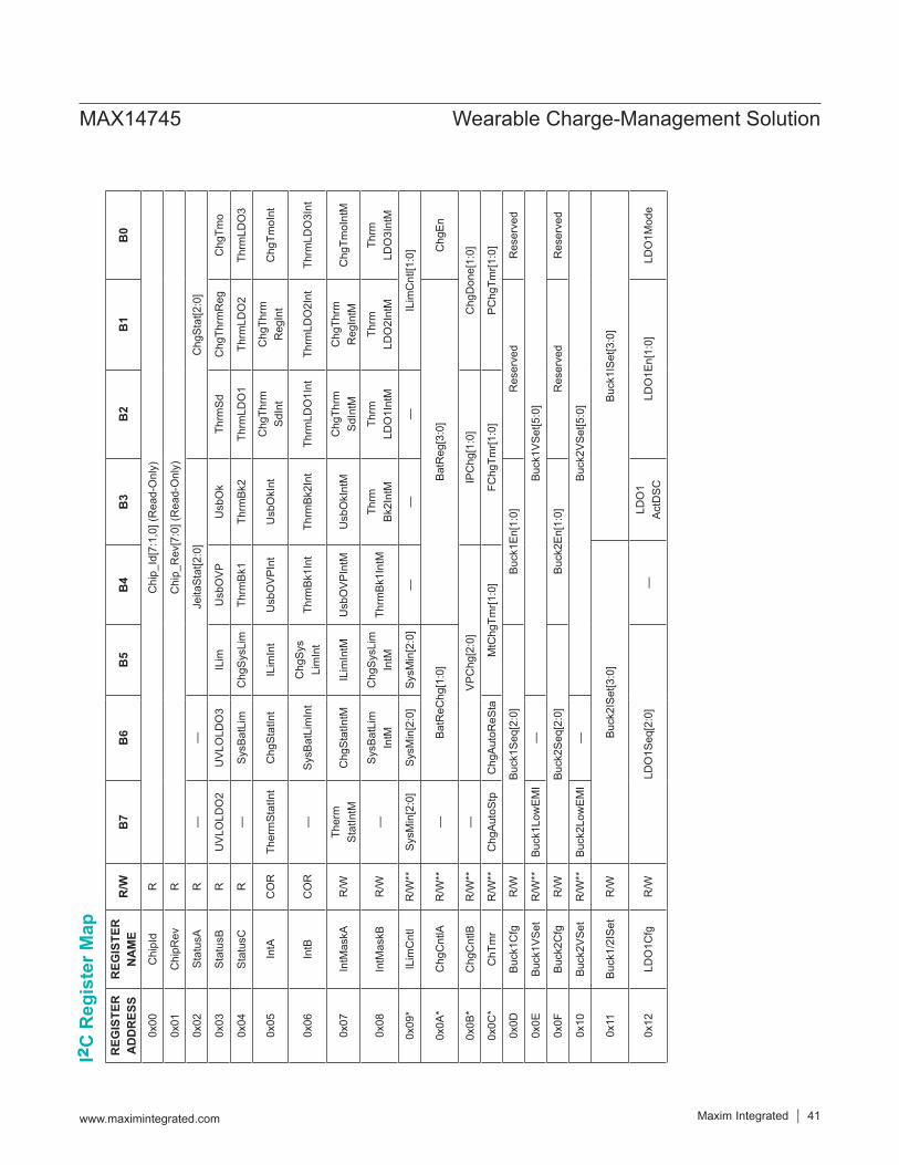
I2C
Reg
iste
r Map
REG
ISTE
R
AD
DR
ESS
REG
ISTE
R
NA
ME
R/W
B7
B6
B5
B4
B3
B2
B1
B0
0x00
Chi
pId
RC
hip_
Id[7
:1,0
] (R
ead-
Onl
y)
0x01
Chi
pRev
RC
hip_
Rev
[7:0
] (R
ead-
Onl
y)
0x02
Stat
usA
R—
—Je
itaSt
at[2
:0]
Chg
Stat
[2:0
]
0x03
Stat
usB
RU
VLO
LDO
2U
VLO
LDO
3IL
imU
sbO
VPU
sbO
kTh
rmSd
Chg
Thrm
Reg
Chg
Tmo
0x04
Stat
usC
R—
SysB
atLi
mC
hgSy
sLim
Thrm
Bk1
Thrm
Bk2
Thrm
LDO
1Th
rmLD
O2
Thrm
LDO
3
0x05
IntA
CO
RTh
erm
Stat
Int
Chg
Stat
Int
ILim
Int
Usb
OVP
Int
Usb
OkI
ntC
hgTh
rm
SdIn
tC
hgTh
rm
Reg
Int
Chg
TmoI
nt
0x06
IntB
CO
R—
SysB
atLi
mIn
tC
hgSy
s Li
mIn
tTh
rmBk
1Int
Thrm
Bk2I
ntTh
rmLD
O1I
ntTh
rmLD
O2I
ntTh
rmLD
O3I
nt
0x07
IntM
askA
R/W
Ther
m
Stat
IntM
Chg
Stat
IntM
ILim
IntM
Usb
OVP
IntM
Usb
OkI
ntM
Chg
Thrm
Sd
IntM
Chg
Thrm
R
egIn
tMC
hgTm
oInt
M
0x08
IntM
askB
R/W
—Sy
sBat
Lim
In
tMC
hgSy
sLim
In
tMTh
rmBk
1Int
MTh
rm
Bk2I
ntM
Thrm
LD
O1I
ntM
Thrm
LD
O2I
ntM
Thrm
LD
O3I
ntM
0x09
*IL
imC
ntl
R/W
**Sy
sMin
[2:0
]Sy
sMin
[2:0
]Sy
sMin
[2:0
]—
——
ILim
Cnt
l[1:0
]
0x0A
*C
hgC
ntlA
R/W
**—
BatR
eChg
[1:0
]Ba
tReg
[3:0
]C
hgEn
0x0B
*C
hgC
ntlB
R/W
**—
VPC
hg[2
:0]
IPC
hg[1
:0]
Chg
Don
e[1:
0]
0x0C
*C
hTm
rR
/W**
Chg
Auto
Stp
Chg
Auto
ReS
taM
tChg
Tmr[1
:0]
FChg
Tmr[1
:0]
PChg
Tmr[1
:0]
0x0D
Buck
1Cfg
R/W
Buck
1Seq
[2:0
]Bu
ck1E
n[1:
0]R
eser
ved
Res
erve
d
0x0E
Buck
1VSe
tR
/W**
Buck
1Low
EMI
—Bu
ck1V
Set[5
:0]
0x0F
Buck
2Cfg
R/W
Buck
2Seq
[2:0
]Bu
ck2E
n[1:
0]R
eser
ved
Res
erve
d
0x10
Buck
2VSe
tR
/W**
Buck
2Low
EMI
—Bu
ck2V
Set[5
:0]
0x11
Buck
1/2I
Set
R/W
Buck
2ISe
t[3:0
]Bu
ck1I
Set[3
:0]
0x12
LDO
1Cfg
R/W
LDO
1Seq
[2:0
]—
LDO
1 Ac
tDSC
LDO
1En[
1:0]
LDO
1Mod
e
MAX14745 Wearable Charge-Management Solution
www.maximintegrated.com Maxim Integrated 41

I2C
Reg
iste
r Map
(con
tinue
d)
Not
e: C
OR
= C
lear
-on-
read
*Reg
iste
r is
rese
t to
defa
ult v
alue
upo
n C
HG
IN ri
sing
edg
e.**
R if
Writ
ePro
tect
ena
bled
(Tab
le 3
8).
All
R/W
regi
ster
s ar
e re
set t
o de
faul
t val
ue w
hen
ente
ring
the
off s
tate
.R
eser
ved
bits
mus
t not
be
mod
ified
from
thei
r def
ault
stat
es to
ens
ure
prop
er o
pera
tion.
REG
ISTE
R
AD
DR
ESS
REG
ISTE
R
NA
ME
R/W
B7
B6
B5
B4
B3
B2
B1
B0
0x13
LDO
1VSe
tR
/W**
——
—LD
O1V
Set[4
:0]
0x14
LDO
2Cfg
R/W
LDO
2Seq
[2:0
]—
LDO
2 Ac
tDSC
LDO
2En[
1:0]
LDO
2Mod
e
0x15
LDO
2VSe
tR
/W**
——
—LD
O2V
Set[4
:0]
0x16
LDO
3Cfg
R/W
LDO
3Seq
[2:0
]—
LDO
3 Ac
tDSC
LDO
3En[
1:0]
LDO
3Mod
e
0x17
LDO
3VSe
tR
/W**
——
—LD
O3V
Set[4
:0]
0x18
*Th
rmC
fgR
/WT1
T2IF
chg[
2:0]
T2T3
IFch
g[2:
0]Th
erm
En[1
:0]
0x19
*Th
rmC
fgR
/W—
——
——
T3T4
IFch
g[2:
0]
0x1A
MO
NC
fgR
/WM
ON
Rat
ioC
fg[1
:0]
MO
NH
iZM
ON
Ctr[
2:0]
0x1B
Boot
Cfg
R/W
PwrR
stC
fg[3
:0]
SftR
stC
fgBo
otD
ly[1
:0]
Chg
Alw
Try
0x1C
PinS
tat
R/W
ILim
_T[2
:0]
—PF
N1
PFN
2M
PC1
MPC
0
0x1D
Buck
1/2E
xtra
R/W
Buck
2IAd
ptEn
bBu
ck2F
stBu
ck2
ActD
scBu
ck2F
FET
Buck
1IAd
ptEn
bBu
ck1F
stBu
ck1A
ctD
SCBu
ck1F
FET
0x1E
PwrC
fgR
/WPF
NxR
esEn
a—
——
——
—St
ayO
n
0x1F
PwrC
md
R/W
PWR
_CM
D
MAX14745 Wearable Charge-Management Solution
www.maximintegrated.com Maxim Integrated 42

I2C Register DescriptionsTable 4. ChipId Register (0x00)
Table 5. ChipRev Register (0x01)
Table 6. StatusA Register (0x02)
ADDRESS: 0x00MODE: Read-OnlyBIT 7 6 5 4 3 2 1 0NAME Chip_Id[7:0]
Chip_Id[7:0] Chip_Id[7:0] bits show information about the version of the MAX14745.
ADDRESS: 0x01MODE: Read-OnlyBIT 7 6 5 4 3 2 1 0NAME Chip_Rev[7:0]
Chip_Rev[7:0] Chip_Rev[7:0] bits show information about the revision of the MAX14745 silicon.
ADDRESS: 0x02MODE: Read-OnlyBIT 7 6 5 4 3 2 1 0NAME — — ThermStat[2:0] ChgStat[2:0]
ThermStat[2:0]
Status of Thermistor Monitoring000 = T < T1001 = T1 < T < T2 010 = T2 < T < T3011 = T3 < T < T4100 = T > T4101 = No thermistor detected (THM high due to external pullup). Note that if a parallel resistor is used for thermistor monitoring, this mode may not function properly.110 = NTC input disabled through ThermEn[1:0]111 = Detection disabled due to CHGIN not present.
ChgStat[2:0]
Status of Charger Mode 000 = Charger off 001 = Charging suspended due to temperature (see Figure 5a and Figure 5b) 010 = Pre-charge in progress 011, 100 = Fast charge in progress101 = Maintain charge in progress 110 = Maintain charger timer done 111 = Charger fault condition (see Figure 5a and Figure 5b)
MAX14745 Wearable Charge-Management Solution
www.maximintegrated.com Maxim Integrated 43

Table 7. StatusB Register (0x03)ADDRESS: 0x03MODE: Read-OnlyBIT 7 6 5 4 3 2 1 0
NAME UVLOLDO2 UVLOLDO3 ILim UsbOVP UsbOk Chg ThrmSd
Chg ThrmReg ChgTmo
UVLOLDO2Status of LDO2 UVLO0 = LDO2 in normal operating mode1 = Undervoltage-lockout on LDO2
UVLOLDO3Status of LDO2 UVLO0 = LDO3 in normal operating mode1 = Undervoltage-lockout on LDO3
ILimCHGIN Input Current Limit 0 = CHGIN input current is within limit.1 = CHGIN input is in current limit.
UsbOVPStatus of CHGIN OVP0 = CHGIN OVP is not active.1 = CHGIN OVP is active.
UsbOkStatus of CHGIN Input 0 = CHGIN Input is not present or outside of valid range.1 = CHGIN Input is present and valid.
ChgThrmSdStatus of Thermal Shutdown 0 = Charger and input current limiter is in normal operating mode.1 = Charger and input current limiter is in thermal shutdown.
ChgThrmReg
Status of Thermal Regulation0 = Charger is functioning normally, or disabled.1 = Charger is running in thermal regulation mode and charging current is being actively reduced to prevent device overheating.
ChgTmoStatus of Time-Out Condition0 = Charger is running normally, or disabled.1 = Charger has reached a time-out condition. ChgStat =1 11 in this condition (see Figure 5).
MAX14745 Wearable Charge-Management Solution
www.maximintegrated.com Maxim Integrated 44

Table 8. StatusC Register (0x04)ADDRESS: 0x04MODE: Read-OnlyBIT 7 6 5 4 3 2 1 0NAME — SysBLim VLim ThrmBuck1 ThrmBuck2 ThrmLDO1 ThrmLDO2 ThrmLDO3
SysBLim
Status of Minimum SYS-BAT Voltage Limit. While the system is powered from VBUS, the charger draws power from SYS to charge the battery. If the total load exceeds the input current limit, an adaptive charger control loop reduces charge current to prevent VSYS from collapsing. The regulation of the charge current starts when either one of the following two conditions is true: 1. VSYS - VBAT = 100mV (typ) OR 2. VSYS = VSYS_LIM (falling)0 = Charge Current is normal.1 = Charge Current is being actively reduced to prevent SYS collapse.
VLim
Status of CHGIN-SYS Voltage Limit. This bit indicates if the input current limit is being actively reduced to maintain a 40mV drop between CHGIN-SYS. This adaptive input current limit prevents adapter collapse in the case that a power adapter with insufficient load capability, or a high resistance charging cable is used.0 = CHGIN input current limit is functioning normally. 1 = CHGIN input current limit is being actively reduced to maintain 40mV drop between CHGIN-SYS.
ThrmBuck1 0 = Buck1 NOT in Thermal Off mode1 = Buck1 in Thermal Off Mode
ThrmBuck2 0 = Buck2 NOT in Thermal Off mode1 = Buck2 in Thermal Off Mode
ThrmLDO1 0 = LDO1 NOT in Thermal Off mode1 = LDO1 in Thermal Off Mode
ThrmLDO2 0 = LDO2 NOT in Thermal Off mode 1 = LDO2 in Thermal Off Mode
ThrmLDO3 0 = LDO3 NOT in Thermal Off mode1 = LDO3 in Thermal Off Mode
MAX14745 Wearable Charge-Management Solution
www.maximintegrated.com Maxim Integrated 45

Table 9. IntA Register (0x05)
Table 10. IntB Register (0x06)
ADDRESS: 0x05MODE: Clear On ReadBIT 7 6 5 4 3 2 1 0
NAME Therm StatInt ChgStatInt ILimInt UsbOVPInt UsbOk Chg
ThrmSdIntTherm RegInt
Chg TmoInt
ThermStatInt Change in ThermStat caused interrupt.
ChgStatInt Change in ChgStat caused interrupt, or first detection complete after POR.
ILimInt Input current limit triggered caused interrupt.
UsbOVPInt Change in UsbOVP caused interrupt.
UsbOk Change in UsbOk caused interrupt.
ChgThrmSdInt Change in ChgThrmSd caused interrupt.
ThermRegInt Change in ChgThrmReg caused interrupt.
ChgTmoInt Change in ChgTmo caused interrupt.
ADDRESS: 0x06MODE: Clear On ReadBIT 7 6 5 4 3 2 1 0
NAME — SysBLimInt VLimInt Thrm Buck1Int
Thrm Buck2Int
Thrm LDO1Int
Thrm LDO2Int
Thrm LDO3Int
SysBLimInt Minimum SYS-BAT voltage limit caused interrupt
VLimInt Input Voltage Limit caused interrupt
ThrmBuck1Int Change in ThrmBuck1 caused interrupt.
ThrmBuck2Int Change in ThrmBuck2 caused interrupt.
ThrmLDO1Int Change in ThrmLDO1 caused interrupt.
ThrmLDO2Int Change in ThrmLDO2 caused interrupt.
ThrmLDO3Int Change in ThrmLDO3 caused interrupt.
MAX14745 Wearable Charge-Management Solution
www.maximintegrated.com Maxim Integrated 46

Table 11. IntMaskA Register (0x07)ADDRESS: 0x07MODE: Read/WriteBIT 7 6 5 4 3 2 1 0
NAME Therm StatIntM
Chg StatIntM ILimIntM Usb
OVPIntM UsbOkM ChgThrm SdIntM
Therm RegIntM
Chg TmoIntM
ThermStatIntMThermStatIntM masks the ThermStatInt interrupt in the IntA register (0x05).0 = Mask1 = Not masked
ChgStatIntMChgStatIntM masks the ChgStatInt interrupt in the IntA register (0x05).0 = Mask1 = Not masked
ILimIntMILimIntM masks the ILimInt interrupt in the IntB register (0x06).0 = Mask1 = Not masked
UsbOVPIntMUsbOVPIntM masks the UsbOVPInt interrupt in the IntA register (0x05).0 = Mask1 = Not masked
UsbOkMUsbOkM masks the UsbOk interrupt in the IntB register (0x06).0 = Mask1 = Not masked
ChgThrm SdIntM
ChgThrmSdIntM masks the ChgThrmSdInt interrupt in the IntB register (0x06).0 = Mask1 = Not masked
ThermRegIntMThermRegIntM masks the ThermRegInt interrupt in the IntA register (0x05).0 = Mask1 = Not masked
ChgTmoIntMChgTmoIntM masks the ChgTmoInt interrupt in the IntA register (0x05).0 = Mask1 = Not masked
MAX14745 Wearable Charge-Management Solution
www.maximintegrated.com Maxim Integrated 47

Table 12. IntMaskB Register (0x08)
Table 13. ILimCntl Register (0x09)
*Register is reset to default value upon CHGIN rising edge.
ADDRESS: 0x08MODE: Read/WriteBIT 7 6 5 4 3 2 1 0
NAME — SysB LimIntM VLimIntM Thrm
Buck1IntMThrm
Buck2IntMThrm
LDO1IntMThrm
LDO2IntMThrm
LDO3IntM
SysBLimIntMSysBLimIntM masks the SysBLimInt interrupt in the IntB register (0x06).0 = Mask1 = Not masked
VLimIntMVLimIntM masks the VLimInt interrupt in the IntB register (0x06).0 = Mask1 = Not masked
ThrmBuck1 IntM
0 = Mask1 = Not masked
ThrmBuck2 IntM
0 = Mask1 = Not masked
ThrmLDO1 IntM
0 = Mask1 = Not masked
ThrmLDO2 IntM
0 = Mask1 = Not masked
ThrmLDO3 IntM
0 = Mask1 = Not masked
ADDRESS: 0x09MODE: Read/Write* or Read-Only if Write-Protect Enabled (see Table 38)BIT 7 6 5 4 3 2 1 0NAME SysMin[2:0] — — — ILimCntl [1:0]
SysMin[2:0]
SysMin sets System Voltage Minimum Threshold. When SYS drops to this level, the charger current is reduced.000 = 3.6V001 = 3.7V010 = 3.8V011 = 3.9V100 = 4.0V101 = 4.1V110 = 4.2V111 = 4.3V
ILimCntl[1:0]
CHGIN Custom Input Current Limit(see Electrical Characteristics table for details)00 = 0mA01 = 100mA 10 = 500mA 11 = 1000mA
MAX14745 Wearable Charge-Management Solution
www.maximintegrated.com Maxim Integrated 48

Table 14. ChgCntlA Register (0x0A)
*Register is reset to default value upon CHGIN rising edge.
ADDRESS: 0x0AMODE: Read/Write* or Ready-Only if Write-Protect Enabled (see Table 38)BIT 7 6 5 4 3 2 1 0NAME BatReChg[1:0] BatReg[3:0] ChgEn
BatReChg[1:0]
Recharge Threshold in Relation to BatReg00 = BatReg - 70mV 01 = BatReg - 120mV 10 = BatReg - 170mV 11 = BatReg - 220mV
BatReg[3:0]
Setting the Battery Regulation Threshold 0000 = 4.05V 0001 = 4.10V 0010 = 4.15V 0011 = 4.20V 0100 = 4.25V 0101 = 4.30V 0110 = 4.35V 0111 = 4.4V 1000 = 4.45V 1001 = 4.5V 1010 = 4.55V 1011 = 4.6V 1100…1111 = Reserved
ChgEnOn/Off Control for Charger (does not affect SYS node). 0 = Charger disabled.1 = Charger enabled.
MAX14745 Wearable Charge-Management Solution
www.maximintegrated.com Maxim Integrated 49

Table 15. ChgCntlB Register (0x0B)
*Register is reset to default value upon CHGIN rising edge.
ADDRESS: 0x0BMODE: Read/Write* or Ready-Only if Write-Protect Enabled (see Table 38)BIT 7 6 5 4 3 2 1 0NAME - VPChg[2:0] IPChg[1:0] ChgDone[1:0]
VPChg[2:0]
Pre-charge voltage threshold setting000 = 2.10V001 = 2.25V010 = 2.40V111 = 2.55V100 = 2.70V101 = 2.85V110 = 3.00V111 = 3.15V
IPChg[1:0]
Pre-charge current setting00 = 0.05 x IFChg01 = 0.1 x IFCHG10 = 0.2 x IFChg11 = 0.3 x IFChg
ChgDone[1:0]
Charge Done Threshold Setting00 = 0.05 x IFChg01 = 0.1 x IFChg10 = 0.2 x IFChg11 = 0.3 x IFChg
MAX14745 Wearable Charge-Management Solution
www.maximintegrated.com Maxim Integrated 50

Table 16. ChTmr Register (0x0C)
Table 17. Buck1Cfg Register (0x0D)*Register is reset to default value upon CHGIN rising edge.
ADDRESS: 0x0CMODE: Read/Write* or Ready-Only if Write-Protect Enabled (see Table 38) BIT 7 6 5 4 3 2 1 0NAME ChgAutoStp ChpAutoReSta MtChgTmr[1:0] FChgTmr[1:0] PChgTmr[1:0]
ChgAutoStpCharger Auto-Stop. Controls the transition from Maintain Charger to Maintain Charger Done.0 = Auto-stop disabled.1 = Auto-stop enabled.
ChgAutoReSta
Charger Auto-Restart Control0 = Charger remains in maintain charge done even when VBAT is less than charge restart threshold (see Charger state diagram) 1 = Charger automatically restarts when VBAT drops below charge restart threshold
MtChgTmr [1:0]
Maintain Charge Timer Setting00 = 0min 01 = 15min 10 = 30min 11 = 60min
FChgTmr[1:0]
Fast-Charge Timer Setting 00 = 75min 01 = 150min 10 = 300min 11 = 600min
PChgTmr[1:0]
Precharge Timer Setting00 = 30min01 = 60min10 = 120min11 = 240min
ADDRESS: 0x0DMODE: Read/WriteBIT 7 6 5 4 3 2 1 0NAME Buck1Seq[2:0] (Read-only) Buck1En[1:0] Reserved Reserved
Buck1Seq[2:0]
Buck1 Enable Configuration (Read-Only)000 = Disabled001 = Reserved010 = Enabled at 0% of Boot/POR Process Delay Control011 = Enabled at 25% of Boot/POR Process Delay Control100 = Enabled at 50% of Boot/POR Process Delay Control 101 = Reserved110 = Reserved111 = Controlled by Buck1En[1:0] after 100% of Boot/POR Process Delay Control
Buck1En[1:0]
Buck1 Enable Configuration (effective only when Buck1Seq = 111)00 = Disabled (Buck1 OUT not actively discharged unless in Hard Reset/ShutDown/Off Mode)01 = Enabled10 = Enabled when MPC0 is high (regardless of MPC1)11 = Enabled when MPC1 is high (regardless of MPC0)
MAX14745 Wearable Charge-Management Solution
www.maximintegrated.com Maxim Integrated 51

Table 18. Buck1VSet Register (0x0E)
Table 19. Buck2Cfg Register (0x0F)
Changes in output voltages are digitally ramped in 25mV increments every 80µs giving a maximum slew rates of 312.5V/s.
ADDRESS: 0x0EMODE: Read/WriteBIT 7 6 5 4 3 2 1 0NAME Buck1LowEMI — Buck1VSet[5:0]
Buck1LowEMIBuck1 BLX Rising/Falling Slopes Setting0 = Normal rising/falling slopes on BLX1 = Reduce the rising/falling slopes on BLX by a factor of three.
Buck1VSet [5:0]
Buck1 Output Voltage SettingLinear Scale from 0.8V to 2.375V in 25mV increments000000 = 0.8V000001 = 0.825V…111111 = 2.375V
ADDRESS: 0x0FMODE: Read/Write or Read-Only if Write-Protect Enabled (See Table 38)BIT 7 6 5 4 3 2 1 0NAME Buck2Seq[2:0] (Read-only) Buck2En[1:0] Reserved Reserved
Buck2Seq[2:0]
Buck2 Enable Configuration (Read-only)000 = Disabled001 = Reserved010 = Enabled at 0% of Boot/POR Process Delay Control011 = Enabled at 25% of Boot/POR Process Delay Control100 = Enabled at 50% of Boot/POR Process Delay Control 101 = Reserved110 = Reserved111 = Controlled by Buck2En [1:0] after 100% of Boot/POR Process Delay Control
Buck2En[1:0]
Buck2 Enable Configuration (effective only when Buck2Seq = 111)00 = Disabled (Buck2 OUT not actively discharged unless in Hard Reset/ShutDown/Off Mode)01 = Enabled10 = Enabled when MPC0 is high (regardless of MPC1)11 = Enabled when MPC1 is high (regardless of MPC0)
MAX14745 Wearable Charge-Management Solution
www.maximintegrated.com Maxim Integrated 52

Table 21. Buck1/2ISet Register (0x11)
Table 20. Buck2VSet Register (0x10)
Changes in output voltages are digitally ramped in 50mV increments every 40µs giving a maximum slew rates of 1250V/s.
ADDRESS: 0x10MODE: Read/Write or Read-Only if WriteProtect Enabled (see Table 38)BIT 7 6 5 4 3 2 1 0NAME Buck2LowEMI — Buck2VSet[5:0]
Buck2LowEMIBuck1 BLX Rising/Falling Slopes Setting0 = Normal rising/falling slopes on BLX1 = Reduce the rising/falling slopes on BLX by a factor of three.
Buck2VSet [5:0]
Buck2 Output Voltage Setting Linear Scale from 0.8V to 3.95V in 50mV increments000000 = 0.80V000001 = 0.85V...111111 = 3.95V
ADDRESS: 0x11MODE: Read/WriteBIT 7 6 5 4 3 2 1 0
NAME Buck2ISet[3:0] Buck1ISet[3:0]
Buck2ISet[3:0]
Buck2 Inductor Peak current setting. 25mA step 0000 = Reserved0001 = Reserved0010 = 50mA... 1111 = 375mA
Buck1ISet[3:0]
Buck1 Inductor Peak Current Setting. 25mA step0000 = Reserved0001 = Reserved0010 = 50mA... 1111 = 375mA
MAX14745 Wearable Charge-Management Solution
www.maximintegrated.com Maxim Integrated 53
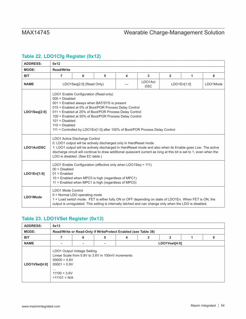
Table 22. LDO1Cfg Register (0x12)
Table 23. LDO1VSet Register (0x13)
ADDRESS: 0x12MODE: Read/WriteBIT 7 6 5 4 3 2 1 0
NAME LDO1Seq[2:0] (Read Only) — LDO1Act DSC LDO1En[1:0] LDO1Mode
LDO1Seq[2:0]
LDO1 Enable Configuration (Read-only)000 = Disabled001 = Enabled always when BAT/SYS is present010 = Enabled at 0% of Boot/POR Process Delay Control011 = Enabled at 25% of Boot/POR Process Delay Control100 = Enabled at 50% of Boot/POR Process Delay Control 101 = Disabled110 = Disabled111 = Controlled by LDO1En[1:0] after 100% of Boot/POR Process Delay Control
LDO1ActDSC
LDO1 Active Discharge Control0: LDO1 output will be actively discharged only in HardReset mode1: LDO1 output will be actively discharged in HardReset mode and also when its Enable goes Low. The active discharge circuit will continue to draw additional quiescent current as long at this bit is set to 1, even when the LDO is disabled. (See EC table.)
LDO1En[1:0]
LDO1 Enable Configuration (effective only when LDO1Seq = 111)00 = Disabled 01 = Enabled10 = Enabled when MPC0 is high (regardless of MPC1)11 = Enabled when MPC1 is high (regardless of MPC0)
LDO1Mode
LDO1 Mode Control0 = Normal LDO operating mode1 = Load switch mode. FET is either fully ON or OFF depending on state of LDO1En. When FET is ON, the output is unregulated. This setting is internally latched and can change only when the LDO is disabled.
ADDRESS: 0x13MODE: Read/Write or Read-Only if WriteProtect Enabled (see Table 38) BIT 7 6 5 4 3 2 1 0NAME - - - LDO1Vset[4:0]
LDO1VSet[4:0]
LDO1 Output Voltage SettingLinear Scale from 0.8V to 3.6V in 100mV increments00000 = 0.8V00001 = 0.9V…11100 = 3.6V>11101 = N/A
MAX14745 Wearable Charge-Management Solution
www.maximintegrated.com Maxim Integrated 54

Table 24. LDO2Cfg Register (0x14)
Table 25. LDO2VSet Register (0x15)
ADDRESS: 0x14MODE: Read/Write or Read-Only if Write-Protect Enabled (See Table 38)BIT 7 6 5 4 3 2 1 0
NAME LDO2Seq[2:0] (Read Only) — LDO2Act DSC LDO2En[1:0] LDO2
Mode
LDO2Seq[2:0]
LDO2 Enable Configuration (Read only)000 = Disabled001 = Enabled always when BAT/SYS is present010 = Enabled at 0% of Boot/POR Process Delay Control011 = Enabled at 25% of Boot/POR Process Delay Control100 = Enabled at 50% of Boot/POR Process Delay Control 101 = Disabled110 = Disabled111 = Controlled by LDO2En[1:0] after 100% of Boot/POR Process Delay Control
LDO2ActDSC
LDO2 Active Discharge Control0 = LDO2 output will be actively discharged only in HardReset mode1 = LDO2 output will be actively discharged in HardReset mode and also when its Enable goes Low. The active discharge circuit will continue to draw additional quiescent current as long at this bit is set to 1, even when the LDO is disabled. (See Electrical Characteristics table.)
LDO2En[1:0]
LDO2 Enable Configuration (effective only when LDO2Seq = 111)00 = Disabled – LDO’s OUT not actively discharged unless HardReset/ShutDown/Off Mode01 = Enabled10 = Enabled when MPC0 is high (regardless of MPC1)11 = Enabled when MPC1 is high (regardless of MPC0)
LDO2Mode
LDO2 Mode Control0 = Normal LDO operating mode1 = Load switch mode. FET is either fully ON or OFF depending on state of LDO2En. When FET is ON, the output is unregulated. This setting is internally latched and can change only when the LDO is disabled.
ADDRESS: 0x15MODE: Read/Write or Read-Only if WriteProtect Enabled (see Table 38)BIT 7 6 5 4 3 2 1 0NAME — — — LDO2Vset[4:0]
LDO2VSet[4:0]
LDO2 Output Voltage SettingLinear Scale from 0.9V to 4.0V in 100mV increments00000 = 0.9V00001 = 1.0V...11111 = 4.0V
MAX14745 Wearable Charge-Management Solution
www.maximintegrated.com Maxim Integrated 55

Table 26. LDO3Cfg Register (0x16)
Table 27. LDO3VSet Register (0x17)
ADDRESS: 0x16
MODE: Read/Write
BIT 7 6 5 4 3 2 1 0
NAME LDO3Seq[2:0] (Read-Only) — LDO3Act DSC LDO3En[1:0] LDO3
Mode
LDO3Seq[2:0]
LDO3 Enable Configuration (Read only)000 = Disabled001 = Enabled always when BAT/SYS is present010 = Enabled at 0% of Boot/POR Process Delay Control011 = Enabled at 25% of Boot/POR Process Delay Control100 = Enabled at 50% of Boot/POR Process Delay Control 101 = Disabled110 = Disabled111 = Controlled by LDO3En[1:0] after 100% of Boot/POR Process Delay Control
LDO3ActDSC
LDO3 Active Discharge Control0 = LDO3 output will be actively discharged only in HardReset mode1 = LDO3 output will be actively discharged in HardReset modes and also when its Enable goes Low. The active discharge circuit will continue to draw additional quiescent current as long at this bit is set to 1, even when the LDO is disabled. (See EC table.)
LDO3En[1:0]
LDO3 Enable Configuration (effective only when LDO3Seq == 111)00 = Disabled. LDO’s OUT not actively discharged unless in HardReset/ShutDown/Off Mode01 = Enabled10 = Enabled when MPC0 is high (regardless of MPC1)11 = Enabled when MPC1 is high (regardless of MPC0)
LDO3Mode
LDO3 Mode Control0 = Normal LDO operating mode1 = Load switch mode. FET is either fully ON or OFF depending on state of LDO3En. When FET is ON, the output is unregulated. This setting is internally latched and can change only when the LDO is disabled.
ADDRESS: 0x17MODE: Read/Write or Read-Only if WriteProtect Enabled (see Table 38)BIT 7 6 5 4 3 2 1 0NAME — — — LDO3Vset[4:0]
LDO3VSet[4:0]
LDO3 Output Voltage SettingLinear Scale from 0.9V to 4.0V in 100mV increments00000 = 0.9V00001 = 1.0V…11111 = 4.0V
MAX14745 Wearable Charge-Management Solution
www.maximintegrated.com Maxim Integrated 56
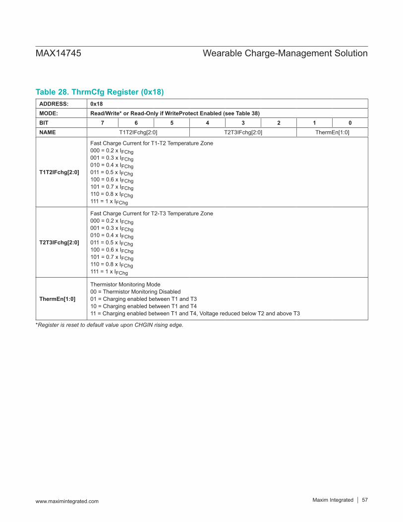
Table 28. ThrmCfg Register (0x18)
*Register is reset to default value upon CHGIN rising edge.
ADDRESS: 0x18MODE: Read/Write* or Read-Only if WriteProtect Enabled (see Table 38)BIT 7 6 5 4 3 2 1 0NAME T1T2IFchg[2:0] T2T3IFchg[2:0] ThermEn[1:0]
T1T2IFchg[2:0]
Fast Charge Current for T1-T2 Temperature Zone 000 = 0.2 x IFChg 001 = 0.3 x IFChg 010 = 0.4 x IFChg 011 = 0.5 x IFChg 100 = 0.6 x IFChg 101 = 0.7 x IFChg 110 = 0.8 x IFChg 111 = 1 x IFChg
T2T3IFchg[2:0]
Fast Charge Current for T2-T3 Temperature Zone 000 = 0.2 x IFChg 001 = 0.3 x IFChg 010 = 0.4 x IFChg 011 = 0.5 x IFChg 100 = 0.6 x IFChg 101 = 0.7 x IFChg 110 = 0.8 x IFChg 111 = 1 x IFChg
ThermEn[1:0]
Thermistor Monitoring Mode00 = Thermistor Monitoring Disabled01 = Charging enabled between T1 and T310 = Charging enabled between T1 and T411 = Charging enabled between T1 and T4, Voltage reduced below T2 and above T3
MAX14745 Wearable Charge-Management Solution
www.maximintegrated.com Maxim Integrated 57
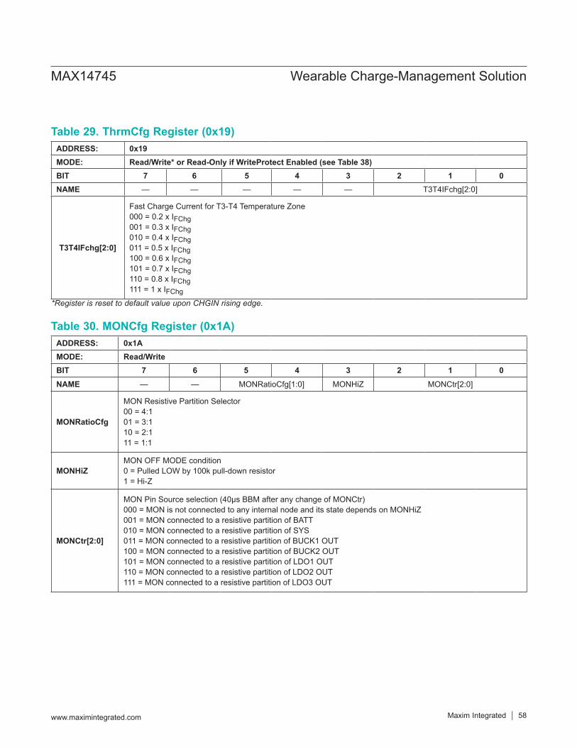
Table 30. MONCfg Register (0x1A)
Table 29. ThrmCfg Register (0x19)
*Register is reset to default value upon CHGIN rising edge.
ADDRESS: 0x19MODE: Read/Write* or Read-Only if WriteProtect Enabled (see Table 38)BIT 7 6 5 4 3 2 1 0NAME — — — — — T3T4IFchg[2:0]
T3T4IFchg[2:0]
Fast Charge Current for T3-T4 Temperature Zone 000 = 0.2 x IFChg 001 = 0.3 x IFChg 010 = 0.4 x IFChg 011 = 0.5 x IFChg 100 = 0.6 x IFChg 101 = 0.7 x IFChg 110 = 0.8 x IFChg 111 = 1 x IFChg
ADDRESS: 0x1AMODE: Read/WriteBIT 7 6 5 4 3 2 1 0NAME — — MONRatioCfg[1:0] MONHiZ MONCtr[2:0]
MONRatioCfg
MON Resistive Partition Selector00 = 4:101 = 3:110 = 2:111 = 1:1
MONHiZMON OFF MODE condition0 = Pulled LOW by 100k pull-down resistor1 = Hi-Z
MONCtr[2:0]
MON Pin Source selection (40µs BBM after any change of MONCtr)000 = MON is not connected to any internal node and its state depends on MONHiZ001 = MON connected to a resistive partition of BATT010 = MON connected to a resistive partition of SYS011 = MON connected to a resistive partition of BUCK1 OUT100 = MON connected to a resistive partition of BUCK2 OUT101 = MON connected to a resistive partition of LDO1 OUT110 = MON connected to a resistive partition of LDO2 OUT111 = MON connected to a resistive partition of LDO3 OUT
MAX14745 Wearable Charge-Management Solution
www.maximintegrated.com Maxim Integrated 58

Table 31. BootCfg Register (0x1B)
Table 32. PinStat Register (0x1C)
ADDRESS: 0x1BMODE: Read-OnlyBIT 7 6 5 4 3 2 1 0NAME PwrRstCfg[3:0] SftRstCfg BootDly[1:0] ChgAlwTry
PwrRstCfg [3:0] See Table 1
SftRstCfgSoft Reset Register Default0 = Registers do not reset to default values on soft reset1 = Registers reset to default values on soft reset
BootDly[1:0]
Reset Delay Control (see Figure 2a, 2b)00 = 80ms01 = 120ms 10 = 220ms 11 = 420ms
ChgAlwTry
UVLO Automatic RetryIf SYS UVLO condition occurs during boot process:0 = Part latches off until CHGIN is removed and replaced1 = Part retries after delay
ADDRESS: 0x1C
MODE: Read Only
BIT 7 6 5 4 3 2 1 0
NAME ILim_T[2:0] - PFN1 PFN2 MPC1 MPC0
ILim_T[2:0]
Monitor of The Input limiter Current Setting000 = Input Limiter Off001 = 100mA010 = 500mA100 =1A
PFN1PFN1 Input State0 = pin low1 = pin high
PFN2PFN2 In/Out State0 = pin low1 = pin high
MPC1MPC1 Input State0 = pin low1 = pin high
MPC0MPC0 Input State0 = pin low1 = pin high
MAX14745 Wearable Charge-Management Solution
www.maximintegrated.com Maxim Integrated 59

Table 33. Buck1/2Extra Control Register (0x1D)ADDRESS: 0x1D
MODE: Read/Write
BIT 7 6 5 4 3 2 1 0
NAME Buck2IAdptEnb Buck2FstBuck2
ActDSCBuck2 FFET
Buck1IAdptEnb Buck1FstBuck1
ActDSCBuck1 FFET
Buck2IAdptEnbBuck 2 Peak Current0 = Enable adaptive peak current1 = Peak current set by Buck2ISet[3:0]
Buck2FstBuck2 Fast Start0 = Normal startup current limit1 = Double the startup current to reduce the startup time by half
Buck2ActDSC
Buck2 Active Discharge Control0 = Buck2 output will be actively discharged only in HardReset mode1 = Buck2 output will be actively discharged in HardReset mode and also when its Enable goes Low. Note, when BuckActDSC=1, the active discharge circuit will remain active and draw additional quiescent current even when Buck2 is disabled.
Buck2FFET Buck2 Force FET scaling (reduces active FET size by 50% and increases efficiency for loads <100mA.)0 = FET Scaling disabled1 = FET Scaling enabled
Buck1IAdptEnbBuck 1 Peak Current0 = Enable adaptive peak current1 = Peak current set by Buck1ISet[3:0]
Buck1FstBuck1 Fast Start0 = Normal startup current limit1 = Double the startup current to reduce the startup time by half
Buck1ActDSC
Buck1 Active Discharge Control0 = Buck1 output will be actively discharged only in HardReset mode1 = Buck1 output will be actively discharged in HardReset mode and also when its Enable goes Low. Note, when BuckActDSC=1, the active discharge circuit will remain active and draw additional quiescent current even when Buck2 is disabled.
Buck1FFET Buck1 Force FET Scaling (reduces active FET size by 50% and increases efficiency for loads <100mA.)0 = FET Scaling only enabled during the Buck1 Turn-On Sequence1 = FET Scaling enabled during the Buck1 Turn-On Sequence and also in the Buck1 Steady ON state
MAX14745 Wearable Charge-Management Solution
www.maximintegrated.com Maxim Integrated 60

Table 35. PwrCmd Register (0x1F)
Table 34. PwrCfg Register (0x1E)ADDRESS: 0x1E
MODE: Read/Write
BIT 7 6 5 4 3 2 1 0
NAME PFNx ResEna – – – – – – StayOn
PFNxResEnaPFN_ PFNx Automatic Internal Pull-Up/Pull-Down Enable0 = No internal pullup/pulldown1 = Automatic internal pullup/pulldown as per Table 1
StayOn
This bit is used to ensure that the processor booted correctly. This bit must be set within 5s of power-on to prevent the part from shutting down and returning to the power-off condition. This bit has no effect after being set.0 = Shut down 5s after power-on1 = Stay on
ADDRESS: 0x1F
MODE: Read/Write
BIT 7 6 5 4 3 2 1 0
NAME PWR_CMD[7:0]
PWR_CMD [7:0]
Power Command RegisterWriting the following values issues the command listed:0xB2 = places the part in off mode0xC3 = issues a hard reset (power cycle)0xD4 = issues a soft reset (reset pulse only)After the written value has been validated by the internal logic, this register is cleared automatically. Any other commands will be ignored. See Table 1 for the available PwrCmd for each PwrRstCfg value.
MAX14745 Wearable Charge-Management Solution
www.maximintegrated.com Maxim Integrated 61

Applications InformationThe buck converters of the MAX14745 are optimized for use with a tiny inductor and small ceramic capacitors. The correct selection of external components ensures high efficiency, low output ripple, and fast transient response.
Inductor SelectionA 2.2µH inductor is recommended for use with the MAX14745 buck converters. Table 36 lists recommended inductors for use depending on whether a given application requires highest efficiency, or a compromise between high efficiency and small size.
Output Capacitor SelectionThe output capacitors of the MAX14745 buck converters are required to keep the output voltage ripple small and to ensure regulation loop stability. A 10µF output capacitor with Buck_ISet[3:0] = 150mA and Buck_IAdptEnb = 0 is suggested to cover all the possible output voltage/load current cases. If a lower output cap are needed, please refer to Table 37 for the minimum allowed capacitor size). Ceramic capacitors are recommended due to their small size and low ESR and care should be taken to ensure that the selected capacitor maintains its capacitance over temperature and voltage bias. Capacitors with X5R or X7R temperature characteristics perform well in most applications.
Input Capacitor SelectionThe input capacitors of the buck converters reduce the current peaks drawn from the battery or input power source and reduces switching noise in the IC. The impedance of the input capacitors at the switching frequency should be kept very low. Ceramic capacitors are recommended due to their small size and low ESR. Make sure the capacitor maintains its capacitance over temperature and DC bias. Capacitors with X5R or X7R temperature characteristics perform well in most applications.
PCB Layout and RoutingHigh switching frequencies and large peak currents make PCB layout a very important part of design. Good design minimizes excessive EMI on the feedback paths and voltage gradients in the ground plane, both of which can result in instability or regulation errors. Connect the inductor, input capacitor, and output capacitor as close together as possible, and keep their traces short, direct, and wide. Connect the two GND pins under the IC and directly to the grounds of the input and output capacitors. Keep noisy traces, such as the LX node, as short as possible.
Table 37. Output Capacitor Values*
Table 36. Suggested Inductors
*Minimum Output Capacitor Values are given for L = 2.2µH
MANUFACTURER SERIES INDUCTANCE (µH)
DC RESISTANCE (mΩ)
CURRENT RATING (mA)
DIMENSIONSL x W x H (mm) NOTES
BOURNS SRP2010 2.2 168 2200 2.0 x 1.6 x 1.0 Optimized for highest efficiency
MURATA MFD160810 2.2 310 1400 1.6 x 0.8 x 1.0 Optimized for smallest size
BUCK_ISET[3:0] OUTPUT VOLTAGE(V)
OUTPUT CAPACITOR MINIMUM VALUES (µF)
<150mA >1.4V 2.2<200mA >1.2V 4.7<175mA >0.8 10
MAX14745 Wearable Charge-Management Solution
www.maximintegrated.com Maxim Integrated 62

Tabl
e 38
. Reg
iste
r Bit
Def
ault
Valu
esRE
GIS
TER
BI
TSM
AX14
745A
MAX
1474
5CM
AX14
745D
MAX
1474
5EM
AX14
745F
MAX
1474
5GM
AX14
745H
MA
X147
45I
MAX
1474
5JM
AX14
745K
Buck
1IZC
Se
t[1:0
]20
mA
30m
A20
mA
20m
A20
mA
30m
A10
mA
30m
A20
mA
20m
A
Buck
1VSe
t [5
:0]
1.2V
1.95
V1.
8V1.
2V1.
2V1.
8V0.
95V
2.37
5V1.
2V1.
2V
Buck
1ISe
t[3:0
]12
5mA
150m
A12
5mA
150m
A12
5mA
125m
A15
0mA
150m
A15
0mA
150m
A
Buck
1En[
1:0]
Dis
able
dD
isab
led
Dis
able
dEn
able
dD
isab
led
Dis
able
dD
isab
led
Enab
led
Dis
able
dD
isab
led
Buck
1Seq
[2:0
]Bu
ck1E
n0%
Boo
tBu
ck1E
n25
% B
oot
Buck
1En
0% B
oot
Buck
1En
Buck
1En
Buck
1En
Buck
1En
Buck
2IZC
Se
t[1:0
]20
mA
40m
A30
mA
30m
A20
mA
20m
A30
mA
30m
A30
mA
30m
A
Buck
2VSe
t [5
:0]
1.8V
3.3V
3V1.
8V1.
8V1.
2V2V
2.7V
2.85
V1.
8V
Buck
2ISe
t[3:0
]12
5mA
150m
A30
0mA
150m
A12
5mA
125m
A15
0mA
150m
A15
0mA
150m
A
Buck
2En[
1:0]
Dis
able
dD
isab
led
Dis
able
dEn
able
dD
isab
led
Dis
able
dEn
able
dD
isab
led
Enab
led
Enab
led
Buck
2Seq
[2:0
]0%
Boo
t50
% B
oot
50%
Boo
t25
% B
oot
0% B
oot
0% B
oot
25%
boo
tBu
ck2E
n25
% B
oot
0% B
oot
LDO
1Mod
eLD
OLD
OSw
itch
LDO
LDO
LDO
LDO
switc
hLD
OLD
OLD
O1V
Set
[4:0
]3V
1.8V
1.8V
1.8V
3V3V
3.1V
0.8V
1.8V
1.8V
LDO
1En[
1:0]
Dis
able
dEn
able
dD
isab
led
Enab
led
Dis
able
dD
isab
led
Dis
able
dD
isab
led
Dis
able
dD
isab
led
LDO
1Seq
[2:0
]LD
O1E
n25
% B
oot
LDO
1En
Alw
ays
On
LDO
1En
LDO
1En
LDO
1En
LDO
1En
LDO
1En
LDO
1En
LDO
2Mod
eSw
itch
LDO
Switc
hLD
OSw
itch
Switc
hSw
itch
LDO
LDO
LDO
LDO
2VSe
t [4
:0]
3.5V
1.8V
1.8V
2.8V
3.5V
3.5V
1.8V
3.2V
1.2V
3V
LDO
2En[
1:0]
Dis
able
dEn
able
dD
isab
led
Enab
led
Dis
able
dD
isab
led
Dis
able
dD
isab
led
Dis
able
dD
isab
led
LDO
2Seq
[2:0
]LD
O2E
n25
% B
oot
LDO
2En
50%
Boo
tLD
O2E
nLD
O2E
nLD
O2E
nLD
O2E
nLD
O2E
nLD
O2E
n
LDO
3Mod
eSw
itch
LDO
Switc
hLD
OSw
itch
Switc
hLD
OLD
OLD
OLD
OLD
O3V
Set
[4:0
]3.
5V1.
8V1.
8V3.
3V3.
5V3.
5V1.
8V2V
3V3V
LDO
3En[
1:0]
Dis
able
dEn
able
dD
isab
led
Enab
led
Dis
able
dD
isab
led
Dis
able
dD
isab
led
Dis
able
dD
isab
led
LDO
3Seq
[2:0
]LD
O3E
n25
% B
oot
LDO
3En
LDO
3En
LDO
3En
LDO
3En
LDO
3En
LDO
3En
LDO
3En
LDO
3En
VPch
g[2:
0]2.
85V
3.00
V2.
85V
3.00
V2.
85V
2.85
V3.
00V
3.00
V3.
00V
3.00
V
IPC
hg[1
:0]
0.10
x
IFC
hg0.
10 x
IF
Chg
0.20
x
IFC
hg0.
20 x
IF
Chg
0.10
x
IFC
hg0.
10 x
IF
Chg
0.10
x
IFC
hg0.
10 x
IF
Chg
0.10
x
IFC
hg0.
20 x
IF
Chg
PChg
Tmr[1
:0]
30m
in12
0min
30m
in30
min
30m
in30
min
60m
in30
min
30m
in30
min
MAX14745 Wearable Charge-Management Solution
www.maximintegrated.com Maxim Integrated 63

Tabl
e 38
. Reg
iste
r Bit
Def
ault
Valu
es (c
ontin
ued)
REG
ISTE
R
BIT
SM
AX14
745A
MAX
1474
5CM
AX14
745D
MAX
1474
5EM
AX14
745F
MAX
1474
5GM
AX14
745H
MAX
1474
5IM
AX14
745J
MAX
1474
5K
FChg
Tmr[1
:0]
300m
in15
0min
600m
in30
0min
300m
in30
0min
300m
in15
0min
150m
in30
0min
MtC
hgTm
r[1:0
]60
min
15m
in0m
in30
min
60m
in60
min
0min
15m
in0m
in30
min
BatR
eg[3
:0]
4.20
V4.
40V
4.35
V4.
20V
4.20
V4.
20V
4.30
V4.
20V
4.20
V4.
35V
BatR
eChg
[1:0
]-1
20m
V‐2
20m
V‐1
20m
V‐1
20m
V-1
00m
V-1
00m
V-1
50m
V-1
00m
V-1
50m
V-1
00m
V
Chg
EnEn
able
dEn
able
dEn
able
dEn
able
dEn
able
dEn
able
dEn
able
dEn
able
dD
isab
led
Enab
led
Chg
Don
e[1:
0]0.
05 x
IF
Chg
0.10
x
IFC
hg0.
05 x
IF
Chg
0.20
x
IFC
hg0.
05 x
IF
Chg
0.05
x
IFC
hg0.
05 x
IF
Chg
0.20
x
IFC
hg0.
05 x
IF
Chg
0.10
x
IFC
hgC
hgAu
toSt
pEn
able
dEn
able
dEn
able
dEn
able
dEn
able
dEn
able
dEn
able
dEn
able
dEn
able
dEn
able
d
Chg
Auto
Sta
Enab
led
Enab
led
Enab
led
Enab
led
Enab
led
Enab
led
Enab
led
Enab
led
Enab
led
Enab
led
Frsh
BatD
isD
one
Cha
rge
Cha
rge
Cha
rge
Don
eD
one
Cha
rge
Cha
rge
Cha
rge
Cha
rge
Ther
mEn
[1:0
]Th
erm
isto
rJE
ITA
1Th
erm
isto
rTh
erm
isto
rJE
ITA
1JE
ITA
1JE
ITA
1Th
erm
isto
rTh
erm
isto
rTh
erm
isto
r
T1_T
2_IF
chg[
2:0]
1.0
x
IFC
hg0.
5 x
IF
Chg
0.5
x
IFC
hg1.
0 x
IF
Chg
1.0
x
IFC
hg1.
0 x
IF
Chg
1.0
x
IFC
hg1.
0 x
IF
Chg
0.2
x
IFC
hg0.
2 x
IF
Chg
T2_T
3_IF
chg[
2:0]
1.0
x IF
Chg
1.0
x
IFC
hg1.
0 x
IF
Chg
1.0
x
IFC
hg1.
0 x
IF
Chg
1.0
x
IFC
hg1.
0 x
IF
Chg
1.0
x
IFC
hg1.
0 x
IF
Chg
1.0
x
IFC
hg
T3_T
4_IF
chg[
2:0]
1.0
x
IFC
hg0.
5 x
IF
Chg
0.2
x
IFC
hg1.
0 x
IF
Chg
1.0
x
IFC
hg1.
0 x
IF
Chg
1.0
x
IFC
hg1.
0 x
IF
Chg
0.2
x
IFC
hg0.
2 x
IF
Chg
Chg
Alw
Try
Ret
ryLa
tch
Off
Latc
h O
ffR
etry
Ret
ryR
etry
Latc
h O
ffR
etry
Ret
ryR
etry
ILim
Cnt
l[1:0
]50
0mA
500m
A50
0mA
500m
A50
0mA
500m
A50
0mA
500m
A10
0mA
500m
A
PwrR
stC
fg[3
:0]
KIN
(011
0)C
R L
ow
(010
1)O
n/O
ff (0
000)
KIN
(011
0)K
IN (0
110)
KIN
(011
0)C
usto
m1
(011
1)C
usto
m2
(100
0)C
usto
m2
(100
0) K
IN(0
110)
PFN
xRes
Ena
Enab
led
Enab
led
Enab
led
Enab
led
Enab
led
Enab
led
Enab
led
Enab
led
Enab
led
Enab
led
Boot
Dly
[1:0
](1
20 +
34)
ms
(120
+ 3
4)m
s(4
20 +
34)
ms
(420
+ 3
4)m
s(1
20 +
34)
ms
(120
+ 3
4)m
s(1
20 +
34)
ms
(80
+ 34
)m
s(1
20 +
34)
ms
(80
+ 34
) m
sSf
tRst
Cfg
Hol
dR
eset
Res
etR
eset
Hol
dH
old
Res
etR
eset
Res
etR
eset
SysM
in[2
:0]
3.6V
3.6V
3.6V
3.6V
3.6V
3.6V
3.6V
3.6V
3.8V
3.6V
Writ
e-Pr
otec
tW
ritab
leW
ritab
leW
ritab
leW
ritab
leW
ritab
leW
ritab
leW
ritab
leW
ritab
leW
ritab
leW
ritab
leSt
ayO
nSt
ay O
nSt
ay O
nSt
ay O
nSt
ay O
nSt
ay O
nSt
ay O
nSt
ay O
nSt
ay O
nSt
ay O
nSt
ay O
n
T1, T
2, T
3, T
40,
10, 2
5,
45°C
0, 1
0, 2
5,
45°C
0, 1
0, 4
5,
60°C
0, 1
0, 4
5,
60°C
0,10
,25,
45
°C0,
10,2
5,45
°C
0,10
,45,
60
°C0,
10,4
5,
60 °C
0,10
,45,
60
°C0,
10,4
5,
60°C
MAX14745 Wearable Charge-Management Solution
www.maximintegrated.com Maxim Integrated 64

Tabl
e 39
. Reg
iste
r Def
ault
Valu
esRE
GIS
TER
ADDR
ESS
REG
ISTE
R NA
ME
MAX
1474
5AM
AX14
745C
MAX
1474
5DM
AX14
745E
MAX
1474
5FM
AX14
745G
MAX
1474
5HM
AX14
745I
MA
X147
45J
MA
X147
45K
0x00
Chi
pId
0x02
0x02
0x02
0x02
0x02
0x02
0x02
0x02
0x02
0x02
0x01
Chi
pRev
0x00
0x00
0x00
0x00
0x00
0x00
0x00
0x00
0x00
0x00
0x07
IntM
askA
0x00
0x00
0x00
0x00
0x00
0x00
0x00
0x00
0x00
0x00
0x08
IntM
askB
0x00
0x00
0x00
0x00
0x00
0x00
0x00
0x00
0x00
0x00
0x09
ILim
Cnt
l0x
020x
020x
020x
020x
020x
020x
020x
020x
410x
02
0x0A
Chg
Cnt
lA0x
270x
6F0x
2D0x
270x
270x
270x
4B0x
270x
460x
2D
0x0B
Chg
Cnt
lB0x
540x
650x
580x
6A0x
540x
540x
640x
660x
640x
69
0x0C
ChT
mr
0xF8
0xD
60x
CC
0xE8
0xF8
0xF8
0xC
90x
D4
0xC
40x
E8
0x0D
Buck
1Cfg
0xE1
0x42
0xE1
0x69
0xE1
0x42
0xE0
0xEA
0xE1
0xE1
0x0E
Buck
1VSe
t0x
100x
2E0x
280x
100x
100x
280x
060x
3F0x
100x
10
0x0F
Buck
2Cfg
0x41
0x83
0x82
0x6A
0x41
0x41
0x6A
0xE2
0x6A
0x4A
0x10
Buck
2Vse
t0x
140x
320x
2C0x
140x
140x
080x
180x
260x
290x
14
0x11
Buck
ISet
0x55
0x66
0xC
50x
660x
550x
550x
660x
660x
660x
66
0x12
LDO
1Cfg
0xE0
0x62
0xE1
0x22
0xE0
0xE0
0xE0
0xE1
0xE0
0xE0
0x13
LDO
1VSe
t0x
160x
0A0x
0A0x
0A0x
160x
160x
170x
000x
0A0x
0A
0x14
LDO
2Cfg
0xE1
0x62
0xE1
0x82
0xE1
0xE1
0xE1
0xE0
0xE0
0xE0
0x15
LDO
2VSe
t0x
1A0x
090x
090x
130x
1A0x
1A0x
090x
170x
030x
15
0x16
LDO
3Cfg
0xE1
0x62
0xE1
0xE2
0xE1
0xE1
0xE0
0xE0
0xE0
0xE0
0x17
LDO
3VSe
t0x
1A0x
090x
090x
180x
1A0x
1A0x
090x
0B0x
150x
15
0x18
THR
MC
FA0x
FD0x
7E0x
7D0x
FD0x
FE0x
FE0x
FE0x
FD0x
1D0x
1D
0x19
THR
MC
FB0x
070x
030x
000x
070x
070x
070x
070x
070x
000x
00
0x1A
MO
NC
FG0x
000x
000x
000x
000x
000x
000x
000x
000x
000x
00
0x1B
BOO
TCFG
0x63
0x5A
0x0E
0x2F
0x63
0x63
0x7A
0x89
0x8B
0x69
0x1D
Buck
1/2
Extra
0x00
0x00
0x00
0x00
0x00
0x00
0x00
0x00
0x00
0x00
0x1E
PwrC
fg0x
810x
810x
810x
810x
810x
810x
810x
810x
810x
81
0x1F
PwrC
md
0x00
0x00
0x00
0x00
0x00
0x00
0x00
0x00
0x00
0x00
MAX14745 Wearable Charge-Management Solution
www.maximintegrated.com Maxim Integrated 65

+Denotes a lead(Pb)-free package/RoHS-compliant package. T = Tape and reel. *Future Product—contact factory for availability. See Table 38 and Table 39 for the device differences.
PART TEMP RANGE PIN-PACKAGEMAX14745AEWX+ -40°C to +85°C 36 WLP
MAX14745AEWX+T -40°C to +85°C 36 WLP
MAX14745BEWX+* -40°C to +85°C 36 WLP
MAX14745BEWX+T* -40°C to +85°C 36 WLP
MAX14745CEWX+ -40°C to +85°C 36 WLP
MAX14745CEWX+T -40°C to +85°C 36 WLP
MAX14745DEWX+ -40°C to +85°C 36 WLP
MAX14745DEWX+T -40°C to +85°C 36 WLP
MAX14745EEWX+ -40°C to +85°C 36 WLP
MAX14745EEWX+T -40°C to +85°C 36 WLP
MAX14745FEWX+ -40°C to +85°C 36 WLP
MAX14745FEWX+T -40°C to +85°C 36 WLP
MAX14745GEWX+ -40°C to +85°C 36 WLP
MAX14745GEWX+T -40°C to +85°C 36 WLP
MAX14745HEWX+* -40°C to +85°C 36 WLP
MAX14745HEWX+T* -40°C to +85°C 36 WLP
MAX14745IEWX+ -40°C to +85°C 36 WLP
MAX14745IEWX+T -40°C to +85°C 36 WLP
MAX14745JEWX+ -40°C to +85°C 36 WLP
MAX14745JEWX+T -40°C to +85°C 36 WLP
MAX14745KEWX+* -40°C to +85°C 36 WLP
MAX14745KEWX+T* -40°C to +85°C 36 WLP
MAX14745 Wearable Charge-Management Solution
www.maximintegrated.com Maxim Integrated 66
Chip InformationPROCESS: BiCMOS
Ordering Information

REVISIONNUMBER
REVISIONDATE DESCRIPTION PAGES
CHANGED0 6/16 Initial release —
1 10/16 Added new part numbers and corrected various errors4–7, 15, 16, 24, 26, 31, 47, 50,
53, 58, 59
2 11/16 Changed future product status of MAX14745C/MAX14745D and various updates 5, 23–25, 36, 46–48, 60
3 3/17 Removed future product asterisks from MAX14745EEWX+ and MAX14745EEWX+T in the Ordering Information table. 61
4 5/17 MAX14745E no longer future product. Updated Table 38 and Table 39 58–61
5 6/17 Removed future product asterisks from MAX14745FEWX+ and MAX14745FEWX+T in the Ordering Information table. 61
6 8/17 Updated Tables 38, 39, and added MAX14745GEWX, MAX14745GEWX+T, MAX14745HEWX, MAX14745HEWX+T to the Ordering Information table 63–66
7 10/17 Removed future product asterisks from MAX14745GEWX+ and MAX14745GEWX+T in the Ordering Information table. 66
8 2/18Added new parts to the Ordering Information table. Updated Tables 23, and 38–39 54, 63–66
9 2/18 Updated Figure 2a, Tables 38–39, and added new future parts to the Ordering Infor-mation table. 30, 63–66
10 4/18 Updated Figures 5a and 5b, and removed future part designation from MAX14745IEWX and MAX14745IEWX+T in the Ordering Information table. 36–37, 66
Maxim Integrated cannot assume responsibility for use of any circuitry other than circuitry entirely embodied in a Maxim Integrated product. No circuit patent licenses are implied. Maxim Integrated reserves the right to change the circuitry and specifications without notice at any time. The parametric values (min and max limits) shown in the Electrical Characteristics table are guaranteed. Other parametric values quoted in this data sheet are provided for guidance.
Maxim Integrated and the Maxim Integrated logo are trademarks of Maxim Integrated Products, Inc.
MAX14745 Wearable Charge-Management Solution
© 2018 Maxim Integrated Products, Inc. 67
Revision History
For pricing, delivery, and ordering information, please contact Maxim Direct at 1-888-629-4642, or visit Maxim Integrated’s website at www.maximintegrated.com.