marvell pxa3xx processor family - toradex · marvell. moving forward faster doc. no. mv-s301374-03,...
TRANSCRIPT

Marvell. Moving Forward Faster
Doc. No. MV-S301374-03, Revision 2.0 Version -
April 6, 2009 Released
Cover
Marvell® PXA3xx Processor FamilyVol.III: Graphics and Input Controller Configuration Developers ManualPXA30x Processor (88AP300, 88AP301, 88AP302, 88AP303)
PXA31x Processor (88AP310, 88AP311, 88AP312)
PXA320 Processor (88AP320, 88AP322)
Document Conventions
Note: Provides related information or information of special importance.
Caution: Indicates potential damage to hardware or software, or loss of data.
Warning: Indicates a risk of personal injury.
Document Status Draft For internal use. This document has not passed a complete technical review cycle and ECN signoff
process.
Preliminary Tapeout (Advance)
This document contains design specifications for a product in its initial stage of design and development. A revision of this document or supplementary information may be published at a later date. Marvell may make changes to these specifications at any time without notice.Contact Marvell Field Application Engineers for more information.
Preliminary Information
This document contains preliminary specifications. A revision of this document or supplementary information may be published at a later date. Marvell may make changes to these specifications at any time without notice. . Contact Marvell Field Application Engineers for more information.
Complete Information
This document contains specifications for a product in its final qualification stages. Marvell may make changes to these specifications at any time without notice. Contact Marvell Field Application Engineers for more information.
Doc Status: Preliminary Technical Publication: 0.xx
X . Y ZMilestone Indicator:Draft = 0.xxAdvance = 1.xxPreliminary = 2.xx Various Revisions Indicator
Work in Progress IndicatorZero means document is released.
For more information, visit our website at: www.marvell.comDisclaimerNo part of this document may be reproduced or transmitted in any form or by any means, electronic or mechanical, including photocopying and recording, for any purpose, without the express written permission of Marvell. Marvell retains the right to make changes to this document at any time, without notice. Marvell makes no warranty of any kind, expressed or implied, with regard to any information contained in this document, including, but not limited to, the implied warranties of merchantability or fitness for any particular purpose. Further, Marvell does not warrant the accuracy or completeness of the information, text, graphics, or other items contained within this document. Marvell products are not designed for use in life-support equipment or applications that would cause a life-threatening situation if any such products failed. Do not use Marvell products in these types of equipment or applications. With respect to the products described herein, the user or recipient, in the absence of appropriate U.S. government authorization, agrees: 1) Not to re-export or release any such information consisting of technology, software or source code controlled for national security reasons by the U.S. Export Control Regulations ("EAR"), to a national of EAR Country Groups D:1 or E:2; 2) Not to export the direct product of such technology or such software, to EAR Country Groups D:1 or E:2, if such technology or software and direct products thereof are controlled for national security reasons by the EAR; and, 3) In the case of technology controlled for national security reasons under the EAR where the direct product of the technology is a complete plant or component of a plant, not to export to EAR Country Groups D:1 or E:2 the direct product of the plant or major component thereof, if such direct product is controlled for national security reasons by the EAR, or is subject to controls under the U.S. Munitions List ("USML"). At all times hereunder, the recipient of any such information agrees that they shall be deemed to have manually signed this document in connection with their receipt of any such information. Copyright © 2009. Marvell International Ltd. All rights reserved. Marvell, the Marvell logo, Moving Forward Faster, Alaska, Fastwriter, Datacom Systems on Silicon, Libertas, Link Street, NetGX, PHYAdvantage, Prestera, Raising The Technology Bar, The Technology Within, Virtual Cable Tester, and Yukon are registered trademarks of Marvell. Ants, AnyVoltage, Discovery, DSP Switcher, Feroceon, GalNet, GalTis, Horizon, Marvell Makes It All Possible, RADLAN, UniMAC, and VCT are trademarks of Marvell. Intel XScale® is a trademark or registered trademark of Intel Corporation or its subsidiaries in the United States and other countries. All other trademarks are the property of their respective owners.
PXA3xx Processor Family Volume III: Graphics and Input Controller Configuration Developers Manual
Doc. No. MV-S301374-03 Revision 2.0 Version -
Copyright © 2009 Marvell
Page 2 April 6, 2009 Released
1234567891011121314151617181920212223242526272829303132333435363738394041424344454647484950515253545556575859

Contents
Copyright © 2009 Marvell Doc. No. MV-S301374-03 Rev. 2.0Version -
April 6, 2009 Released Page 3
12345678910111213141516171819202122232425262728293031323334353637383940414243444546474849505152535455565758
Contents
1 LCD Controller .............................................................................................................................23
1.1 PXA3xx Processor Differences .......................................................................................................................23
1.2 Features ..........................................................................................................................................................23
1.3 Signals ............................................................................................................................................................25
1.4 Operation ........................................................................................................................................................251.4.1 Block Diagram ..................................................................................................................................26
1.4.1.1 Temporal Modulated Energy Distribution (TMED) Dithering ..............................................291.4.1.2 Input FIFOs ........................................................................................................................311.4.1.3 Lookup Palette ...................................................................................................................321.4.1.4 Output FIFO .......................................................................................................................32
1.4.2 Pixel Clock Frequency Calculation ...................................................................................................321.4.3 Bandwidth Calculations ....................................................................................................................331.4.4 Graphical Overlays ...........................................................................................................................35
1.4.4.1 Transparency .....................................................................................................................371.4.5 Pixel Formats ....................................................................................................................................37
1.4.5.1 Data Format for Pixel Depths of 8 bpp ...............................................................................401.4.5.2 Data Format for RGB Color Space.....................................................................................411.4.5.3 Data Format for YCbCr Color Space..................................................................................44
1.4.6 Base Frame ......................................................................................................................................461.4.7 Overlay 1 Window.............................................................................................................................461.4.8 Overlay 2 Window.............................................................................................................................47
1.4.8.1 Bilinear Interpolation...........................................................................................................491.4.8.2 Color Space Conversion from YCbCr to RGB Format .......................................................501.4.8.3 Color Space Conversion from 24 bpp to 16, 18, and 19 bpp RGB Formats ......................50
1.4.9 Interfacing with LCD Smart Panels ...................................................................................................511.4.9.1 Read Command .................................................................................................................52
1.4.10 Hardware Cursor ..............................................................................................................................531.4.10.1 32 × 32 × 2 bpp and 64 × 64 × 2 bpp 2-Color and Transparency Modes ...........................541.4.10.2 32 × 32 × 2 bpp and 64 × 64 × 2 bpp 4-Color Modes .........................................................541.4.10.3 32 × 32 × 2 bpp and 64 × 64 × 2 bpp 3-Color and Transparency Mode .............................551.4.10.4 128×128×1 bpp 2-Color Mode............................................................................................551.4.10.5 128 × 128 × 1 bpp 1-Color and Transparency Mode..........................................................551.4.10.6 Cursor Positioning ..............................................................................................................551.4.10.7 Cursor Color Map ...............................................................................................................57
1.4.11 External Palette Buffer ......................................................................................................................571.4.11.1 Palette Data Formats .........................................................................................................571.4.11.2 Little-Endian Format ...........................................................................................................58
1.4.12 Frame Buffer .....................................................................................................................................591.4.12.1 Memory Organization for Pixel Depth of 8 bpp ..................................................................601.4.12.2 Memory Organization for Pixel Depth of 16 bpp ................................................................601.4.12.3 Memory Organization for Pixel Depth of 18 bpp ................................................................601.4.12.4 Memory Organization for Pixel Depth of 19 bpp ................................................................621.4.12.5 Memory Organization for Pixel Depth of 24 bpp ................................................................631.4.12.6 Memory Organization for Pixel Depth of 25 bpp ................................................................631.4.12.7 Memory Organization for 4:4:4 YCbCr Packed Format......................................................64
1.4.13 Functional Timing .............................................................................................................................641.4.13.1 Passive Mode Timing .........................................................................................................641.4.13.2 Active Mode Timing............................................................................................................661.4.13.3 Smart Panel Mode Timing..................................................................................................68

PXA3xx (88AP3xx) Processor FamilyVolume III: Graphics and Input Controller Configuration Developers Manual
Doc. No. MV-S301374-03 Rev. 2.0 Version -
Copyright © 2009 Marvell
Page 4 April 6, 2009 Released
12345678910111213141516171819202122232425262728293031323334353637383940414243444546474849505152535455565758
1.4.14 Using the LCD Controller Data Pins .................................................................................................691.4.14.1 16-Bit Interface for Active ..................................................................................................701.4.14.2 18-bit Interface for Active ...................................................................................................711.4.14.3 24-bit Interface for Active for PXA31x ................................................................................711.4.14.4 Summary of Pin Assignments in Active Mode....................................................................711.4.14.5 8-Bit Interface for Smart Panels .........................................................................................72
1.5 LCD Controller Register Descriptions .............................................................................................................721.5.0.1 Register Summary..............................................................................................................73
1.5.1 LCD Controller Control Register 0 (LCCR0).....................................................................................761.5.2 LCD Controller Control Register 1 (LCCR1).....................................................................................851.5.3 LCD Controller Control Register 2 (LCCR2).....................................................................................881.5.4 LCD Controller Control Register 3 (LCCR3).....................................................................................901.5.5 LCD Controller Control Register 4 (LCCR4).....................................................................................971.5.6 LCD Controller Control Register 5 (LCCR5)...................................................................................1051.5.7 LCD Controller Control Register 6 (LCCR6)...................................................................................1121.5.8 Overlay 1 Control Register 1 (OVL1C1) .........................................................................................1131.5.9 Overlay 1 Control Register 2 (OVL1C2) .........................................................................................1141.5.10 Overlay 2 Control Register 1 (OVL2C1) .........................................................................................1151.5.11 Overlay 2 Control Register 2 (OVL2C2) .........................................................................................1171.5.12 Cursor Control Register (CCR) .......................................................................................................1171.5.13 Command Control Register (CMDCR)............................................................................................1181.5.14 TMED RGB Seed Register (TRGBR) .............................................................................................1191.5.15 TMED Control Register (TCR)........................................................................................................1201.5.16 DMA Frame Descriptor Address Registers (FDADRx) ...................................................................1221.5.17 DMA Frame Branch Registers (FBRx)............................................................................................1221.5.18 Panel Read Status Register (PRSR) ..............................................................................................1231.5.19 LCD Controller Status Register 0 (LCSR0).....................................................................................1241.5.20 LCD Controller Status Register 1 (LCSR1).....................................................................................1311.5.21 LCD Controller Interrupt ID Register (LIIDR) ..................................................................................1391.5.22 DMA Frame Source Address Registers (FSADRx) ........................................................................1391.5.23 DMA Frame ID Registers (FIDRx) ..................................................................................................1401.5.24 LCD DMA Command Register (LDCMDx)......................................................................................141
2 Mini-LCD Controller...................................................................................................................145
2.1 PXA3xx Processor Differences .....................................................................................................................145
2.2 Features ........................................................................................................................................................146
2.3 Signals ..........................................................................................................................................................146
2.4 Operation ......................................................................................................................................................1472.4.1 Input Pixel Formats.........................................................................................................................1472.4.2 Mini-LCD Output Interface ..............................................................................................................1482.4.3 Power Manager Interface ...............................................................................................................1482.4.4 Mini-LCD Input FIFO.......................................................................................................................1492.4.5 Functional Timing ...........................................................................................................................149
2.5 Register Descriptions ....................................................................................................................................1502.5.0.1 Register Summary............................................................................................................151
2.5.1 Mini-LCD Controller Control Register 0 (MLCCR0) ........................................................................1512.5.2 Mini-LCD Controller Control Register 1 (MLCCR1) ........................................................................1532.5.3 Mini-LCD Controller Control Register 2 (MLCCR2) ........................................................................1552.5.4 Mini-LCD SRAM Address Register (MLSADD)...............................................................................1562.5.5 Mini-LCD Frame Count Register (MLFRMCNT) .............................................................................157

Contents
Copyright © 2009 Marvell Doc. No. MV-S301374-03 Rev. 2.0Version -
April 6, 2009 Released Page 5
12345678910111213141516171819202122232425262728293031323334353637383940414243444546474849505152535455565758
3 Quick Capture Interface ............................................................................................................159
3.1 PXA3xx Processor Differences .....................................................................................................................160
3.2 Features ........................................................................................................................................................160
3.3 Signals ..........................................................................................................................................................161
3.4 Operation ......................................................................................................................................................1613.4.1 Functional Units ..............................................................................................................................164
3.4.1.1 Histogram Unit (HST) .......................................................................................................1643.4.1.2 Pixel Substitution Unit (PSU)............................................................................................1653.4.1.3 Compand and Gamma Correction (CGC) ........................................................................1673.4.1.4 Spatial Scaling Unit (SSU) ...............................................................................................1693.4.1.5 Color Synthesis Unit (CSU)..............................................................................................1723.4.1.6 Color Management Unit (CMU)........................................................................................174
3.4.2 4:2:0 Downsampling (PXA31x processor only) ..............................................................................1783.4.3 Operating Modes ............................................................................................................................178
3.4.3.1 Master-Parallel (MP) Internal Synchronization Mode.......................................................1783.4.3.2 JPEG Mode (PXA31x processor only) .............................................................................1793.4.3.3 Slave-Parallel (SP) External Synchronization Mode ........................................................181
3.4.4 Clock Generation ............................................................................................................................1833.4.5 FIFO Operation...............................................................................................................................183
3.4.5.1 FIFO Data Packing...........................................................................................................1843.4.5.2 DMA Data Transfers from FIFOs .....................................................................................1843.4.5.3 Overflow Handling ............................................................................................................1853.4.5.4 Trailing Bytes....................................................................................................................185
3.4.6 Pixel Formats ..................................................................................................................................1863.4.6.1 RAW Pixel Data Formats .................................................................................................1863.4.6.2 RAW 8-Bit Data Format....................................................................................................1863.4.6.3 RAW 10-Bit Data Format..................................................................................................1863.4.6.4 Preprocessed YCbCr Pixel Data Formats........................................................................1873.4.6.5 Data Capture Sequence for YCbCr Formats....................................................................187
3.4.7 Frame Synchronization...................................................................................................................1883.4.7.1 Frame Rotation.................................................................................................................1883.4.7.2 Frame Non-Rotation.........................................................................................................189
3.5 Register Descriptions ....................................................................................................................................1893.5.1 Register Summary ..........................................................................................................................1893.5.2 Quick Capture Interface Control Register 0 (CICR0)......................................................................1933.5.3 Quick Capture Interface Control Register 1 (CICR1)......................................................................1983.5.4 Quick Capture Interface Control Register 2 (CICR2)......................................................................2013.5.5 Quick Capture Interface Control Register 3 (CICR3)......................................................................2023.5.6 Quick Capture Interface Control Register 4 (CICR4)......................................................................2043.5.7 Quick Capture Interface Timeout Register (CITOR).......................................................................2063.5.8 Quick Capture Interface Status Register (CISR) ............................................................................2073.5.9 Quick Capture Interface Return Clock Delay Register (CIRCD).....................................................2103.5.10 Quick Capture JPEG Control and Status Register (CIJPEG) .........................................................2133.5.11 Quick Capture Interface Receive Buffer Register 0 (CIBR0) ..........................................................2133.5.12 Quick Capture Interface Receive Buffer Register 1 (CIBR1) ..........................................................2143.5.13 Quick Capture Interface Receive Buffer Register 2 (CIBR2) ..........................................................2143.5.14 Quick Capture Interface Receive Buffer Register 3 (CIBR3) ..........................................................2153.5.15 Quick Capture Interface Pixel Substitution Status Register (CIPSS)..............................................2153.5.16 Quick Capture Interface Pixel Substitution Buffer (CIPBUF) ..........................................................2163.5.17 Quick Capture Interface Histogram Configuration (CIHST) ............................................................2173.5.18 Quick Capture Interface Histogram Summation Register (CISUM)................................................2183.5.19 Quick Capture Interface Companding Configuration Register (CICCR) .........................................2193.5.20 Quick Capture Interface Spatial Scaling Configuration Register (CISSC) ......................................220

PXA3xx (88AP3xx) Processor FamilyVolume III: Graphics and Input Controller Configuration Developers Manual
Doc. No. MV-S301374-03 Rev. 2.0 Version -
Copyright © 2009 Marvell
Page 6 April 6, 2009 Released
12345678910111213141516171819202122232425262728293031323334353637383940414243444546474849505152535455565758
3.5.21 Quick Capture Interface Color Management Register (CICMR).....................................................2203.5.22 Color Management Coefficient 0 Register (CICMC0).....................................................................2213.5.23 Color Management Coefficient 1 Register (CICMC1).....................................................................2223.5.24 Color Management Coefficient 2 Register (CICMC2).....................................................................2233.5.25 Quick Capture Interface FIFO Status Register (CIFSR) .................................................................2243.5.26 Quick Capture Interface FIFO Control Register 0 (CIFR0).............................................................2273.5.27 Quick Capture Interface FIFO Control Register 1 (CIFR1).............................................................2293.5.28 Quick Capture Interface Controller DMA Registers ........................................................................229
3.5.28.1 DMA Descriptors ..............................................................................................................2293.5.28.2 Quick Capture Interface DMA Descriptor Address Registers (CIDADRx)........................2303.5.28.3 Quick Capture Interface DMA Source Address Registers (CISADRx) .............................2303.5.28.4 Quick Capture Interface DMA Target Address Registers (CITADRx) ..............................2313.5.28.5 Quick Capture Interface DMA Command Registers (CICMDx)........................................2313.5.28.6 Quick Capture Interface DMA Branch Registers (CIDBRx)..............................................2333.5.28.7 DMA Channel Control/Status Register (CIDCSRx) ..........................................................234
4 Graphics Controller...................................................................................................................237
4.1 Features ........................................................................................................................................................237
4.2 I/O Signals.....................................................................................................................................................237
4.3 System Overview ..........................................................................................................................................237
4.4 Buffer Operation Overview............................................................................................................................2384.4.1 Programming the Source Buffer Registers .....................................................................................2394.4.2 Programming the Destination Buffer Registers ..............................................................................240
4.5 Functional Description...................................................................................................................................2414.5.1 Control Functions............................................................................................................................2424.5.2 Programming Environment .............................................................................................................243
4.5.2.1 Interrupts ..........................................................................................................................2434.5.3 Error Conditions: Crash Stops, Breakpoints, and Aborts................................................................244
4.5.3.1 Crash Stop .......................................................................................................................2444.5.3.2 Breakpoint Out .................................................................................................................2444.5.3.3 Breakpoint In ....................................................................................................................2444.5.3.4 Target Aborts....................................................................................................................2444.5.3.5 Master Aborts ...................................................................................................................2454.5.3.6 Internal Operation Errors..................................................................................................2454.5.3.7 Stop Execution .................................................................................................................2454.5.3.8 Abort Execution ................................................................................................................245
4.5.4 Low Power (S0/D1/C2 and S0/D2/C2) ...........................................................................................2464.5.5 2-D Graphics Instruction Buffers.....................................................................................................246
4.5.5.1 Basic Queue Structure Operation ....................................................................................2464.5.5.2 Ring Buffer .......................................................................................................................2484.5.5.3 Batch Buffers....................................................................................................................2524.5.5.4 Display Front and Back Buffers........................................................................................255
4.5.6 Graphics Instruction List .................................................................................................................2554.5.7 Pixel Data Formats .........................................................................................................................257
4.5.7.1 Pixel Data Memory Organization......................................................................................2584.5.7.2 Pixel Type Conversion .....................................................................................................261
4.5.8 2-D Address Generation .................................................................................................................2714.5.9 Reading Extra Pixels ......................................................................................................................2724.5.10 Color Saturation..............................................................................................................................272
4.5.10.1 Fractional Pixel Addressing..............................................................................................273

Contents
Copyright © 2009 Marvell Doc. No. MV-S301374-03 Rev. 2.0Version -
April 6, 2009 Released Page 7
12345678910111213141516171819202122232425262728293031323334353637383940414243444546474849505152535455565758
4.5.11 Limitations on Pixel Operations ......................................................................................................2734.5.11.1 Cacheable Memory ..........................................................................................................2734.5.11.2 Clipping ............................................................................................................................2734.5.11.3 Pixel Operations for Indexed Color Pixel Formats ...........................................................273
4.6 Graphics Controller Instruction Set ...............................................................................................................2734.6.1 Control and Memory Interface Instructions.....................................................................................273
4.6.1.1 Batch Buffer Start (GC_BBST).........................................................................................2744.6.1.2 Batch Buffer End (GC_BBEND) ......................................................................................2754.6.1.3 Buffer Info (GC_BUFFI)....................................................................................................2764.6.1.4 Load Register (GC_LREG) ..............................................................................................2774.6.1.5 NOP (GC_NOP) ...............................................................................................................2794.6.1.6 Destination (Display) Buffer Flip Immediate (GC_DBFLIP)..............................................2804.6.1.7 Store Register (GC_STREG) ...........................................................................................2824.6.1.8 Interrupt (GC_INT) ...........................................................................................................2834.6.1.9 Wait for Event (GC_WAIT) ...............................................................................................284
4.6.2 2-D Graphics Instructions ...............................................................................................................2864.6.2.1 Format for 2-D Instructions...............................................................................................2864.6.2.2 Color Fill ...........................................................................................................................2884.6.2.3 Chroma Key BLT..............................................................................................................2904.6.2.4 Line Draw .........................................................................................................................2934.6.2.5 Anti-Aliased Line Draw .....................................................................................................3064.6.2.6 Stretch BLT ......................................................................................................................3124.6.2.7 Alpha Blend BLT ..............................................................................................................3164.6.2.8 Scale BLT.........................................................................................................................3214.6.2.9 Bias BLT...........................................................................................................................3244.6.2.10 Rotate BLT .......................................................................................................................3274.6.2.11 Raster Operation BLT ......................................................................................................3314.6.2.12 Pattern Copy BLT.............................................................................................................3374.6.2.13 Decimate BLT...................................................................................................................341
4.7 Register Descriptions ....................................................................................................................................3444.7.0.1 Register Summary............................................................................................................344
4.7.1 Graphics Controller Configuration Register (GCCR) ......................................................................3484.7.2 Graphics Controller Interrupt Status Control Register (GCISCR) ...................................................3504.7.3 Graphics Controller Interrupt Enable Control Register (GCIECR)..................................................3524.7.4 Graphics Controller NOP ID Register (GCNOPID).........................................................................3544.7.5 Graphics Controller Default Alpha Setting Register (GCALPHASET) ............................................3554.7.6 Graphics Controller Default Transparency Setting Register (GCTSET) .........................................3564.7.7 Graphics Controller Ring Buffer Base Address Register (GCRBBR) .............................................3574.7.8 Graphics Controller Ring Buffer Length Register (GCRBLR) .........................................................3574.7.9 Graphics Controller Ring Buffer Head Register (GCRBHR)...........................................................3584.7.10 Graphics Controller Ring Buffer Tail Register (GCRBTR) ..............................................................3584.7.11 Graphics Controller Ring Buffer Execution Head Register (GCRBEXHR) .....................................3594.7.12 Graphics Controller Batch Buffer Base Address Register (GCBBBR)............................................3594.7.13 Graphics Controller Batch Buffer Head Register (GCBBHR) .........................................................3604.7.14 Graphics Controller Batch Buffer Execution Head Register (GCBBEXHR)....................................3604.7.15 Graphics Controller Destination Buffer 0 (Display Buffer 0) Base Address Register (GCD0BR) ...3614.7.16 Graphics Controller Destination Buffer 0 (Display Buffer 0) Step Size Register (GCD0STP) ........3614.7.17 Graphics Controller Destination Buffer 0 (Display Buffer 0) Stride Size Register (GCD0STR) ......3624.7.18 Graphics Controller Destination Buffer 0 (Display Buffer 0) Pixel Format Register (GCD0PF) ......3624.7.19 Graphics Controller Destination Buffer 1 (Display Buffer 1) Base Address Register (GCD1BR) ...3634.7.20 Graphics Controller Destination Buffer 1 (Display Buffer 1) Step Size Register (GCD1STP) ........3634.7.21 Graphics Controller Destination Buffer 1 (Display Buffer 1) Stride Size Register (GCD1STR) ......3644.7.22 Graphics Controller Destination Buffer 1 (Display Buffer 1) Pixel Format Register (GCD1PF) ......3644.7.23 Graphics Controller Destination Buffer 2 Base Address Register (GCD2BR) ................................3654.7.24 Graphics Controller Destination Buffer 2 Step Size Register (GCD2STP) .....................................365

PXA3xx (88AP3xx) Processor FamilyVolume III: Graphics and Input Controller Configuration Developers Manual
Doc. No. MV-S301374-03 Rev. 2.0 Version -
Copyright © 2009 Marvell
Page 8 April 6, 2009 Released
12345678910111213141516171819202122232425262728293031323334353637383940414243444546474849505152535455565758
4.7.25 Graphics Controller Destination Buffer 2 Stride Size Register (GCD2STR) ...................................3664.7.26 Graphics Controller Destination Buffer 2 Pixel Format Register (GCD2PF)...................................3664.7.27 Graphics Controller Source 0 Base Address Register (GCS0BR)..................................................3674.7.28 Graphics Controller Source 0 Step Size Register (GCS0STP).......................................................3674.7.29 Graphics Controller Source 0 Stride Size Register (GCS0STR) ....................................................3684.7.30 Graphics Controller Source 0 Pixel Format Register (GCS0PF) ....................................................3684.7.31 Graphics Controller Source 1 Base Address Register (GCS1BR)..................................................3694.7.32 Graphics Controller Source 1 Step Size Register (GCS1STP).......................................................3694.7.33 Graphics Controller Source 1 Stride Size Register (GCS1STR) ....................................................3704.7.34 Graphics Controller Source 1 Pixel Format Register (GCS1PF) ....................................................3704.7.35 Graphics Controller Pixel ALU Scratch Registers (GCSC[0:7]_WD[0:1]) .......................................3714.7.36 Graphics Controller Control Read/Write Illegal Access Bad Address Register (GCCABADDR)....3714.7.37 Graphics Controller Target Abort Address Register (GCTABADDR) .............................................3724.7.38 Graphics Controller Master Abort Address Register (GCMABADDR)............................................372
5 Keypad Controller .....................................................................................................................375
5.1 PXA3xx Processor Differences .....................................................................................................................375
5.2 Features ........................................................................................................................................................375
5.3 Signals ..........................................................................................................................................................376
5.4 Keypad Controller Operation.........................................................................................................................3775.4.1 Matrix Keypad Interface..................................................................................................................378
5.4.1.1 Manual Matrix Scan..........................................................................................................3785.4.1.2 Automatic Matrix Scan Initiated by Keypad Activity .........................................................3795.4.1.3 Automatic Matrix Scan Initiated By Software ...................................................................379
5.4.2 Direct-Key Interface ........................................................................................................................3795.4.2.1 Direct Keys .......................................................................................................................3795.4.2.2 Rotary Encoders...............................................................................................................380
5.4.3 Debounce Check ............................................................................................................................3805.4.3.1 Matrix Keypad, Manual Scan Procedure..........................................................................3805.4.3.2 Matrix Keypad, Automatic Scan Procedure......................................................................3815.4.3.3 Direct Keypad Procedure .................................................................................................381
5.4.4 Interrupt Generation........................................................................................................................3815.4.5 Low Power Operation and Wakeup ................................................................................................381
5.5 Register Descriptions ....................................................................................................................................3825.5.0.1 Register Summary............................................................................................................382
5.5.1 Keypad Control (KPC) Register ......................................................................................................3835.5.2 Keypad Direct Key (KPDK) Register ..............................................................................................3875.5.3 Keypad Rotary Encoder Count (KPREC) Register .........................................................................3885.5.4 Keypad Matrix Key (KPMK) Register..............................................................................................3895.5.5 Keypad Interface Automatic Scan (KPAS) Register .......................................................................3895.5.6 Keypad Interface Automatic Scan Multiple Keypress (KPASMKPx) Registers 0:3 ........................390
5.5.6.1 Keypad Automatic Scan Multiple Keypress register 0 (KPASMKP0)...............................3905.5.6.2 Keypad Automatic Scan Multiple Keypress register 1 (KPASMKP1)...............................3905.5.6.3 Keypad Automatic Scan Multiple Keypress register 2 (KPASMKP2)...............................3915.5.6.4 Keypad Automatic Scan Multiple Keypress register 3 (KPASMKP3)...............................391
5.5.7 Keypad Key-Debounce Interval (KPKDI) Register .........................................................................393
6 Hardware Video Accelerator Unit.............................................................................................395
6.1 PXA3xx Processor Differences .....................................................................................................................395
6.2 Features ........................................................................................................................................................395
6.3 Signals ..........................................................................................................................................................396
6.4 Block Diagram...............................................................................................................................................396

Contents
Copyright © 2009 Marvell Doc. No. MV-S301374-03 Rev. 2.0Version -
April 6, 2009 Released Page 9
12345678910111213141516171819202122232425262728293031323334353637383940414243444546474849505152535455565758
6.4.1 System Connectivity .......................................................................................................................3976.4.2 Encoding Pipeline ...........................................................................................................................397
6.4.2.1 Integer Pixel Motion Estimation (IPE) ..............................................................................3986.4.2.2 Sub-pixel Motion Search Engine (SPE) and Intra/Inter Prediction ...................................3986.4.2.3 Residual Generation and Compression Units ..................................................................3986.4.2.4 Microcontroller Unit ..........................................................................................................3986.4.2.5 De-blocking Engine ..........................................................................................................398
6.4.3 Decoding Pipeline...........................................................................................................................3996.4.3.1 Command Control Unit .....................................................................................................3996.4.3.2 Inverse Transform and Inverse Zigzag Units ...................................................................3996.4.3.3 De-blocking Filter Unit ......................................................................................................3996.4.3.4 Motion Compensation Unit ...............................................................................................400
6.5 Functional Description...................................................................................................................................4006.5.1 Encoder Flow..................................................................................................................................4006.5.2 Decoder Flow..................................................................................................................................4016.5.3 Synchronization ..............................................................................................................................4026.5.4 Hardware/Software Mapping for Different Standards .....................................................................4026.5.5 Low-Power Mode............................................................................................................................403
6.6 Encode Commands.......................................................................................................................................404
6.7 Decode Commands ......................................................................................................................................404
6.8 De-block Commands.....................................................................................................................................404
6.9 Hardware Video Accelerator Registers .........................................................................................................404
6.10 Related Documents.......................................................................................................................................405

PXA3xx (88AP3xx) Processor FamilyVolume III: Graphics and Input Controller Configuration Developers Manual
Doc. No. MV-S301374-03 Rev. 2.0 Version -
Copyright © 2009 Marvell
Page 10 April 6, 2009 Released
12345678910111213141516171819202122232425262728293031323334353637383940414243444546474849505152535455565758

Figures
Copyright © 2009 Marvell Doc. No. MV-S301374-03 Rev. 2.0Version -
April 6, 2009 Released Page 11
12345678910111213141516171819202122232425262728293031323334353637383940414243444546474849505152535455565758
Figures
Figure 1: LCD Controller Block Diagram..........................................................................................................27
Figure 2: LCD Outputs for Active and Passive Displays..................................................................................29
Figure 3: Temporal Dithering Concept .............................................................................................................30
Figure 4: Compare Range for TMED ...............................................................................................................30
Figure 5: TMED Block Diagram .......................................................................................................................31
Figure 6: Hardware Cursor, Base Plus 2 Overlays Displayed on LCD Panel .................................................36
Figure 7: Luminance and Chrominance Samples in 4:4:4 YCbCr Video Frame..............................................45
Figure 8: Luminance and Chrominance Samples in 4:2:2 Video Frame..........................................................45
Figure 9: Luminance and Chrominance Samples in 4:2:0 YCbCr Video Frame..............................................46
Figure 10: Overlay 1 Frame Buffer Format .......................................................................................................47
Figure 11: Overlay 2 Frame Buffer Format for 4:4:4 YCbCr Packed Format.....................................................49
Figure 12: Overlay 2 Frame Buffer Format for YCbCr Planar Format ...............................................................49
Figure 13: Interface to LCD Smart Panel with Internal Frame Buffer.................................................................51
Figure 14: Cursor Position within Display Frame...............................................................................................57
Figure 15: Palette Data Formats—Transparency Disabled ...............................................................................57
Figure 16: Palette Data Formats 0b01—Transparency Enabled .......................................................................58
Figure 17: Palette Data Formats 0b10—Transparency Enabled .......................................................................58
Figure 18: Palette Data Formats 0b11—Transparency Enabled .......................................................................58
Figure 19: Format for Palette Data ....................................................................................................................58
Figure 20: Memory Organization for Pixel Depth of 8 bpp.................................................................................60
Figure 21: Memory Organization for Pixel Depth of 16 bpp...............................................................................60
Figure 22: Memory Organization for Pixel Depth of 18 bpp Unpacked..............................................................60
Figure 23: Memory Organization for Pixel Depth of 18 bpp Unpacked in (6R+2’0s, 6G+2’0s, 6B+2’0s) Format ..............................................................................................................................................61
Figure 24: Memory Organization for Pixel Depth of 18 bpp Packed..................................................................61
Figure 25: Memory Organization for Pixel Depth of 18 bpp Packed in (6R+2’0s, 6G+2’0s, 6B+2’0s)..............61
Figure 26: Memory Organization for Pixel Depth of 19 bpp Unpacked..............................................................62
Figure 27: Memory Organization for Pixel Depth of 19bpp Unpacked in (6R+2’0s, 6G+2’0s, 6B+2’0s) Format ..............................................................................................................................................62
Figure 28: Memory Organization for Pixel Depth of 19 bpp Packed..................................................................62
Figure 29: Memory Organization for Pixel Depth of 24 bpp...............................................................................63
Figure 30: Memory Organization for Pixel Depth of 25 bpp...............................................................................63
Figure 31: Memory Organization for 4:4:4 YCbCr Packed Format ....................................................................64
Figure 32: LCD Controller Pin Timing ................................................................................................................65
Figure 33: Passive Mode End-of-Frame Timing ................................................................................................66
Figure 34: Active Mode Timing ..........................................................................................................................67
Figure 35: Active Mode Pixel Clock and Data Pin Timing..................................................................................68
Figure 36: Interface with SMART Panels Timing ...............................................................................................69
Figure 37: LCD Data-Pin Pixel Ordering............................................................................................................70
Figure 38: Mini-LCD Controller Interface .........................................................................................................145

PXA3xx (88AP3xx) Processor FamilyVolume III: Graphics and Input Controller Configuration Developers Manual
Doc. No. MV-S301374-03 Rev. 2.0 Version -
Copyright © 2009 Marvell
Page 12 April 6, 2009 Released
12345678910111213141516171819202122232425262728293031323334353637383940414243444546474849505152535455565758
Figure 39: Mini-LCD Controller Pin Timing Diagram........................................................................................150
Figure 40: Active Mode Pixel Clock and Data Pin Timing................................................................................150
Figure 41: Quick Capture Interface Block Diagram .........................................................................................162
Figure 42: Histogram Unit Block Diagram........................................................................................................165
Figure 43: Example of Pixel Substitution Applied to a Bayer Pattern ..............................................................166
Figure 44: Coarseness and Residual Bit Fields...............................................................................................168
Figure 45: 2:1 Scaling Filter .............................................................................................................................170
Figure 46: (a) Bayer Pattern Color Filter Array (CFA) and (b) 24-Bit Color .....................................................172
Figure 47: Color Interpolation of Bayer Pattern ...............................................................................................173
Figure 48: Fractional Format for Color-Correction Coefficients .......................................................................175
Figure 49: Extraction of Final Result for Each Color Component ....................................................................176
Figure 50: Fractional Representation for CSC Coefficients .............................................................................176
Figure 51: Extraction of Final Result for CSC ..................................................................................................177
Figure 52: YCbCr 4:2:2 Chroma Sub-Sampling in Horizontal Dimension........................................................177
Figure 53: Master-Parallel (MP) Internal Synchronization ModeMaster-Parallel (MP) State Diagram ............179
Figure 54: Slave-Parallel State Diagram..........................................................................................................182
Figure 55: Basic Processor Architecture .........................................................................................................238
Figure 56: General Graphics Controller Buffer Configuration ..........................................................................239
Figure 57: Programming Flow for Source Buffers Registers............................................................................240
Figure 58: Programming Flow for Destination Buffers Registers .....................................................................241
Figure 59: Empty Queue (Head = Tail) ............................................................................................................247
Figure 60: Queue of Length 8 Containing 6 Instructions (Tail – Head = 6)......................................................247
Figure 61: Basic Write to Queue (Tail = Tail + 1); Full Queue (Tail + 1 – Length = Head) ..............................247
Figure 62: Basic Read from Queue (Head = Head + 1)...................................................................................248
Figure 63: Wrap-around Write to Queue (new Tail = 0); Full Queue (Tail + 1 = Head) ...................................248
Figure 64: Programming New Tail in Wrap-Around Mode ...............................................................................249
Figure 65: Ring Buffer Before Graphics Controller Execution Wrap ...............................................................250
Figure 66: Ring Buffer After Graphics Controller Execution Wrap..................................................................251
Figure 67: Ring Buffer Double Buffered Implementation ................................................................................252
Figure 68: Basic Batch Buffer Call ...................................................................................................................253
Figure 69: Chained Batch Buffer Call ..............................................................................................................254
Figure 70: End of Buffer Interrupt Generation During Batch Buffer Execution ................................................255
Figure 71: 2-D Address Generation Block Diagram.........................................................................................271
Figure 72: Illegal Addressing for 2-D Graphics Instructions.............................................................................286
Figure 73: Color Fill Operation.........................................................................................................................288
Figure 74: Chroma Key BLT Operation ...........................................................................................................290
Figure 75: Line Draw Operation.......................................................................................................................293
Figure 76: Use of Programmable Values for Line Draw ..................................................................................295
Figure 77: Line Draw Algorithm Rules .............................................................................................................296
Figure 78: Examples of Line Draw DelX, DelY, and Length ............................................................................300
Figure 79: Detailed drawing of Resulting Line (With Boerne Line DX0 = 4.0) .................................................302
Figure 80: Detailed drawing of Resulting Line (With Boerne Line DX0 = 3.5) .................................................302
Figure 81: Anti-Aliased Line Draw Operation...................................................................................................306
Figure 82: Effects of Anti-Aliased Line Drawing...............................................................................................307

Figures
Copyright © 2009 Marvell Doc. No. MV-S301374-03 Rev. 2.0Version -
April 6, 2009 Released Page 13
12345678910111213141516171819202122232425262728293031323334353637383940414243444546474849505152535455565758
Figure 83: Example of Anti-Aliased commands ...............................................................................................307
Figure 84: Drawing of Resulting Anti-Aliased Line from Example 5 (DX0 = 4.0) .............................................308
Figure 85: Drawing of Resulting Anti-Aliased Line from Example 5 (DX0 = 3.5) .............................................308
Figure 86: Stretch BLT Operation ....................................................................................................................312
Figure 87: Alpha Blend BLT Operation ............................................................................................................316
Figure 88: Scale BLT Operation ......................................................................................................................321
Figure 89: Bias BLT Operation ........................................................................................................................324
Figure 90: Rotate BLT Operation.....................................................................................................................327
Figure 91: Raster Operation BLT Operation ....................................................................................................331
Figure 92: Pattern Copy BLT Operation Option 1............................................................................................337
Figure 93: Pattern Copy BLT Operation Option 2............................................................................................338
Figure 94: Decimate BLT Operation ................................................................................................................341
Figure 95: Keypad Interface Diagram to 8 × 8 Matrix Keys, 6 Direct Keys, Rotary Encoder ...........................377
Figure 96: Rotary Encoder...............................................................................................................................380
Figure 97: Hardware Video Accelerator Unit Block Diagram ...........................................................................397
Figure 98: Encoding Pipeline and Hardware Video Accelerator Unit Block Diagram ......................................397
Figure 99: Decoding Pipeline...........................................................................................................................399
Figure 100: Video Encoder Operational Flow ....................................................................................................400
Figure 101: Video Decoder Operational Flow....................................................................................................402

PXA3xx (88AP3xx) Processor FamilyVolume III: Graphics and Input Controller Configuration Developers Manual
Doc. No. MV-S301374-03 Rev. 2.0 Version -
Copyright © 2009 Marvell
Page 14 April 6, 2009 Released
12345678910111213141516171819202122232425262728293031323334353637383940414243444546474849505152535455565758

Tables
Copyright © 2009 Marvell Doc. No. MV-S301374-03 Rev. 2.0Version -
April 6, 2009 Released Page 15
12345678910111213141516171819202122232425262728293031323334353637383940414243444546474849505152535455565758
Tables
Table 1: PXA3xx Processors Feature Differences .........................................................................................23
Table 2: LCD Controller I/O Signal Descriptions ............................................................................................25
Table 3: DMA Channel Use ............................................................................................................................28
Table 4: Display Order of Three Layers and Cursor on LCD Panel................................................................36
Table 5: Overlay Support for Bits-per-Pixel (bpp) Formats.............................................................................37
Table 6: Bits-per-Pixel Format Combinations Allowed....................................................................................38
Table 7: Video Sampling Formats Supported by Overlay 2............................................................................39
Table 8: Valid Pixel Formats for Each Frame .................................................................................................39
Table 9: Valid Combinations of PDFOR and PAL_FOR for Various Base bpp ..............................................39
Table 10: Palette Entries for 8 bpp Format.......................................................................................................41
Table 11: Standard RGB and RGBT Formats ..................................................................................................41
Table 12: Pixel Depth of 16 Bits-per-Pixel with Overlays Disabled...................................................................41
Table 13: Pixel Depth of 16 Bits-per-Pixel with Overlays Enabled ...................................................................42
Table 14: PXA31x processor Only: Pixel Depth of 16 Bits with Overlays and Chroma-Keying Enabled..........42
Table 15: Pixel Depth of 18 Bits-per-Pixel with Overlays Disabled...................................................................42
Table 16: PXA31x processor Only: Pixel Depth of 18 Bits-per-Pixel in (6R+2’0, 6G+2’0, 6B+2’0) Format with Overlays Disabled .....................................................................................................................42
Table 17: Pixel Depth of 19 Bits-per-Pixel with Overlays Enabled ...................................................................43
Table 18: PXA31x processor Only: Pixel Depth of 19 Bits-per-Pixel (6R+2’0, 6G+2’0, 6B+2’0) format with Overlays Enabled ......................................................................................................................43
Table 19: Pixel Depth of 24 Bits-per-Pixel with Overlays Disabled...................................................................43
Table 20: Pixel Depth of 24 Bits-per-Pixel with Overlays Enabled ...................................................................44
Table 21: Pixel Depth of 25 Bits-per-Pixel with Overlays Enabled ...................................................................44
Table 22: YCbCr 4:4:4 Packed Pixel Data Format Stored in Memory..............................................................49
Table 23: Packing and Precision for Conversion from RGB 8:8:8 to RGB 5:5:5 ..............................................51
Table 24: Color Component Precision Conversions After Color Space Conversion ........................................51
Table 25: Command Data Format ....................................................................................................................52
Table 26: Command Description ......................................................................................................................52
Table 27: Control Bit Description ......................................................................................................................53
Table 28: Command Data Format Stored in Memory.......................................................................................53
Table 29: Pixel Data 32×32×2 bpp and 64×64×2 bpp 2-Color and Transparency Modes ................................54
Table 30: Pixel Data 32×32×2 bpp and 64×64×2 bpp 4-Color Modes ..............................................................54
Table 31: Pixel Data 32×32×2 bpp and 64×64×2 bpp 3-Color and Transparency Modes ................................55
Table 32: Pixel Data 128×128×1 bpp 2-Color Mode.........................................................................................55
Table 33: Pixel Data 128×128×1 bpp 1-Color and Transparency Mode...........................................................55
Table 34: LCD Controller Data Pin Usage........................................................................................................70
Table 35: Color, Passive, 8-Bit Bus ..................................................................................................................70
Table 36: Color, Active, 16 bpp, 16-Bit Bus......................................................................................................70
Table 37: Color, Active, 18 bpp or 19 bpp, 18-Bit Bus......................................................................................71
Table 38: Color, Active, 24 bpp or 25 bpp, 24-Bit Bus......................................................................................71

PXA3xx (88AP3xx) Processor FamilyVolume III: Graphics and Input Controller Configuration Developers Manual
Doc. No. MV-S301374-03 Rev. 2.0 Version -
Copyright © 2009 Marvell
Page 16 April 6, 2009 Released
12345678910111213141516171819202122232425262728293031323334353637383940414243444546474849505152535455565758
Table 39: Pin Assignments in Active Mode ......................................................................................................71
Table 40: 8-Bit Interface for Smart Panels .......................................................................................................72
Table 41: LCD Controller Register Summary ...................................................................................................73
Table 42: LCCR0 Bit Definitions .......................................................................................................................77
Table 43: LCCR1 Bit Definitions .......................................................................................................................86
Table 44: LCCR2 Bit Definitions .......................................................................................................................88
Table 45: LCCR3 Bit Definitions .......................................................................................................................91
Table 46: LCCR4 Bit Definitions .......................................................................................................................98
Table 47: LCCR5 Bit Definitions .....................................................................................................................106
Table 48: LCCR6 Bit Definitions .....................................................................................................................112
Table 49: OVL1C1 Bit Definitions ...................................................................................................................113
Table 50: OVL1C2 Bit Definitions ...................................................................................................................114
Table 51: OVL2C1 Bit Definitions ...................................................................................................................115
Table 52: OVL2C2 Bit Definitions ...................................................................................................................117
Table 53: CCR Bit Definitions .........................................................................................................................118
Table 54: CMDCR Bit Definitions ...................................................................................................................119
Table 55: TRGBR Bit Definitions ....................................................................................................................119
Table 56: TCR Bit Definitions .........................................................................................................................120
Table 57: FDADR0/1/2/3/4/5/6 Bit Definitions ................................................................................................122
Table 58: FBR0/1/2/3/4/5/6 Bit Definitions......................................................................................................123
Table 59: PRSR Bit Definitions.......................................................................................................................124
Table 60: LCSR0 Bit Definitions .....................................................................................................................125
Table 61: LCSR1 Bit Definitions .....................................................................................................................132
Table 62: LIIDR Bit Definitions........................................................................................................................139
Table 63: FSADR0/1/2/3/4/5/6 Bit Definitions.................................................................................................140
Table 64: FIDR0/1/2/3/4/5/6 Bit Definitions ....................................................................................................140
Table 65: LDCMD0/1/2/3/4/5/6 Bit Definitions ................................................................................................141
Table 66: PXA3xx Processors Feature Differences .......................................................................................145
Table 67: Mini-LCD Interface Signals .............................................................................................................146
Table 68: RGB 5:5:5 Pixel Format, Count Value Enable Bit Cleared .............................................................147
Table 69: Pixel Format - Count Value Enable Bit Set .....................................................................................147
Table 70: Pixel Value with Count Value Enable Bit Set to 1 ...........................................................................147
Table 71: Memory Organization for Pixel Data...............................................................................................148
Table 72: Output Data Bus ............................................................................................................................148
Table 73: Mini-LCD Controller Register Summary..........................................................................................151
Table 74: MLCCR0 Bit Definitions ..................................................................................................................151
Table 75: MLCCR1 Bit Definitions ..................................................................................................................154
Table 76: MLCCR2 Bit Definitions ..................................................................................................................155
Table 77: MLSADD Bit Definitions..................................................................................................................156
Table 78: MLFRMCNT Bit Definitions.............................................................................................................157
Table 79: PXA3xx Processors Feature Differences .......................................................................................160
Table 80: Quick Capture Interface Signals .....................................................................................................161
Table 81: Quick Capture Interface Functional Units .......................................................................................162
Table 82: Active Resources for RAW and Preprocessed Image Capture ......................................................163

Tables
Copyright © 2009 Marvell Doc. No. MV-S301374-03 Rev. 2.0Version -
April 6, 2009 Released Page 17
12345678910111213141516171819202122232425262728293031323334353637383940414243444546474849505152535455565758
Table 83: DMA Channel Use ..........................................................................................................................164
Table 84: Color Tag LUT Address Mapping ...................................................................................................167
Table 85: Pixel Bit Field Allowable Ranges ....................................................................................................168
Table 86: Summary of Scaling Formula .........................................................................................................171
Table 87: Scaling Examples ...........................................................................................................................171
Table 88: Quick Capture Interface Modes of Operation .................................................................................178
Table 89: FIFO Operation Data ......................................................................................................................183
Table 90: Memory Organization for RAW 8-Bit Data......................................................................................186
Table 91: Memory Organization for RAW 10-Bit Data....................................................................................186
Table 92: 8-Bit Data Capture Sequence for YCbCr 4:2:2 Color Space ..........................................................187
Table 93: Memory Organization for 4:2:0 (PXA31x processor only) and 4:2:2 YCbCr Planarized Format ....188
Table 94: Quick Capture Interface Register Summary ...................................................................................190
Table 95: CICR0 Bit Definitions ......................................................................................................................193
Table 96: CICR1 Bit Definitions ......................................................................................................................199
Table 97: CICR2 Bit Definitions ......................................................................................................................201
Table 98: CICR3 Bit Definitions ......................................................................................................................202
Table 99: CICR4 Bit Definitions ......................................................................................................................204
Table 100: CITOR Bit Definitions......................................................................................................................207
Table 101: CISR Bit Definitions ........................................................................................................................207
Table 102: CIRCD Bit Definitions .....................................................................................................................211
Table 103: CIJPEG Bit Definitions....................................................................................................................213
Table 104: CIBR0 Bit Definitions ......................................................................................................................214
Table 105: CIBR1 Bit Definitions ......................................................................................................................214
Table 106: CIBR2 Bit Definitions ......................................................................................................................215
Table 107: CIBR3 Bit Definitions ......................................................................................................................215
Table 108: CIPSS Bit Definitions ......................................................................................................................216
Table 109: CIPBUF Bit Definitions....................................................................................................................217
Table 110: CIHST Bit Definitions ......................................................................................................................217
Table 111: CISUM Bit Definitions .....................................................................................................................218
Table 112: CICCR Bit Definitions .....................................................................................................................219
Table 113: CISSC Bit Definitions......................................................................................................................220
Table 114: CICMR Bit Definitions .....................................................................................................................220
Table 115: CICMC0 Bit Definitions ...................................................................................................................221
Table 116: CICMC1 Bit Definitions ...................................................................................................................222
Table 117: CICMC2 Bit Definitions ...................................................................................................................223
Table 118: CIFSR Bit Definitions ......................................................................................................................224
Table 119: CIFR0 Bit Definitions ......................................................................................................................227
Table 120: CIFR1 Bit Definitions ......................................................................................................................229
Table 121: CIDADRx Bit Definitions .................................................................................................................230
Table 122: CISADRx Bit Definitions .................................................................................................................231
Table 123: CITADRx Bit Definitions..................................................................................................................231
Table 124: CICMDx Bit Definitions ...................................................................................................................232
Table 125: CICMD3 Bit Definitions ...................................................................................................................233
Table 126: CIFBRx Bit Definitions ....................................................................................................................234

PXA3xx (88AP3xx) Processor FamilyVolume III: Graphics and Input Controller Configuration Developers Manual
Doc. No. MV-S301374-03 Rev. 2.0 Version -
Copyright © 2009 Marvell
Page 18 April 6, 2009 Released
12345678910111213141516171819202122232425262728293031323334353637383940414243444546474849505152535455565758
Table 127: CIDCSRx Bit Definitions .................................................................................................................235
Table 128: ........................................................................................................................................................252
Table 129: Graphics Controller Control and Memory Interface Instructions.....................................................256
Table 130: Graphics Controller 2-D Graphics Instructions ...............................................................................256
Table 131: Standard RGB Pixel Data Formats .................................................................................................257
Table 132: 8-Bit Lookup Table Index Packed Pixel Storage (Optimum Step Size = 1 byte) ............................258
Table 133: 15-Bit RGB 5:5:5 Packed Pixel Storage (Optimum Step Size = 2 bytes) .......................................258
Table 134: 16-Bit RGBT 5:5:5:1 Packed Pixel Storage (Optimum Step Size = 2 bytes) ..................................258
Table 135: 16-Bit RGB 5:6:5 Packed Pixel Storage (Optimum Step Size = 2 bytes) .......................................259
Table 136: 18-Bit RGB 6:6:6 Unpacked Pixel Storage (Step Size = 4 bytes)...................................................259
Table 137: 18-Bit RGB 6:6:6 Packed Pixel Storage (Optimum Step Size = 3 bytes) .......................................259
Table 138: 19-Bit RGBT 6:6:6 Unpacked Pixel Storage (Step Size = 4 bytes) ................................................259
Table 139: 19-Bit RGBT 6:6:6 Packed Pixel Storage (Optimum Step Size = 3 bytes) .....................................259
Table 140: 24-Bit RGB 8:8:8 Unpacked Pixel Storage (Step Size = 4 bytes)...................................................260
Table 141: 24-Bit RGB 8:8:8 Packed Pixel Storage (Optimum Step Size = 3 bytes) .......................................260
Table 142: 24-Bit RGBA 6:6:6:6 Unpacked Pixel Storage (Step Size = 4 bytes) .............................................260
Table 143: 24-Bit RGBA 6:6:6:6 Packed Pixel Storage (Optimum Step Size = 3 bytes)..................................260
Table 144: 25-Bit RGBT 8:8:8:1 Unpacked Pixel Storage (Step Size = 4 bytes) .............................................260
Table 145: 32-Bit RGBA 8:8:8:8 Packed Pixel Storage (Optimum Step Size = 4 bytes)..................................261
Table 146: 48-Bit RGB 16:16:16 Unpacked Pixel Storage (Step Size = 8 bytes).............................................261
Table 147: 64-Bit RGBA 16:16:16:16 Packed Pixel Storage (Optimum Step Size = 8 bytes)..........................261
Table 148: Transparency to Alpha Conversion ................................................................................................262
Table 149: Alpha to Transparency Conversion ................................................................................................262
Table 150: Conversion from 8-Bit Lookup Table Index to RGBA 16:16:16:16 .................................................262
Table 151: Conversion from 15-Bit RGB 5:5:5 to RGBA 16:16:16:16 ..............................................................262
Table 152: Conversion from 16-Bit RGBT 5:5:5:1 to RGBA 16:16:16:16.........................................................263
Table 153: Conversion from 16-Bit RGB 5:6:5 to RGBA 16:16:16:16 ..............................................................263
Table 154: Conversion from 18-Bit RGB 6:6:6 to RGBA 16:16:16:16 ..............................................................264
Table 155: Conversion from 19-Bit RGBT 6:6:6:1 to RGBA 16:16:16:16.........................................................264
Table 156: Conversion from 24-Bit RGB 8:8:8 to RGBA 16:16:16:16 ..............................................................264
Table 157: Conversion from 24-Bit RGBA 6:6:6:6 to RGBA 16:16:16:16.........................................................265
Table 158: Conversion from 25-Bit RGBT 8:8:8:1 to RGBA 16:16:16:16.........................................................265
Table 159: Conversion from 32-Bit RGBA 8:8:8:8 to RGBA 16:16:16:16.........................................................265
Table 160: Conversion from 48-Bit RGB 16:16:16 to RGBA 16:16:16:16 ........................................................266
Table 161: Conversion from 64-Bit RGBA 16:16:16:16 to RGBA 16:16:16:16.................................................266
Table 162: Conversion from RGBA 16:16:16:16 to 8-bit Lookup Table Index..................................................266
Table 163: Conversion from RGBA 16:16:16:16 to 15-bit RGB 5:5:5 ..............................................................267
Table 164: Conversion from RGBA 16:16:16:16 to 16-bit RGBT 5:5:5:1 .........................................................267
Table 165: Conversion from RGBA 16:16:16:16 to 16-bit RGB 5:6:5 ..............................................................268
Table 166: Conversion from RGBA 16:16:16:16 to 18-bit RGB 6:6:6 ..............................................................268
Table 167: Conversion from RGBA 16:16:16:16 to 19-bit RGBT 6:6:6:1 .........................................................268
Table 168: Conversion from RGBA 16:16:16:16 to 24-bit RGB 8:8:8 ..............................................................269
Table 169: Conversion from RGBA 16:16:16:16 to 24-bit RGBA 6:6:6:6 .........................................................269
Table 170: Conversion from RGBA 16:16:16:16 to 25-bit RGBT 8:8:8:1 .........................................................269

Tables
Copyright © 2009 Marvell Doc. No. MV-S301374-03 Rev. 2.0Version -
April 6, 2009 Released Page 19
12345678910111213141516171819202122232425262728293031323334353637383940414243444546474849505152535455565758
Table 171: Conversion from RGBA 16:16:16:16 to 32-bit RGBA 8:8:8:8 .........................................................270
Table 172: Conversion from RGBA 16:16:16:16 to 48-bit RGB 16:16:16 ........................................................270
Table 173: Conversion from RGBA 16:16:16:16 to 64-bit RGBA 16:16:16:16 .................................................270
Table 174: Extra Bytes Read per Memory Line Based on Step Size ...............................................................272
Table 175: General Instruction Encoding for Control and Memory Interface Instructions ................................274
Table 176: Batch Buffer Start Instruction Encoding.........................................................................................275
Table 177: Batch Buffer End Instruction Encoding ..........................................................................................276
Table 178: Buffer Info Instruction Encoding.....................................................................................................276
Table 179: Load Register Instruction Encoding................................................................................................278
Table 180: NOP Instruction Encoding ..............................................................................................................280
Table 181: Destination Buffer Flip Immediate Operation Based on Qualifiers..................................................281
Table 182: Destination (Display) Buffer Flip Immediate Instruction Encoding..................................................281
Table 183: Store Register Instruction Encoding ...............................................................................................282
Table 184: Interrupt Instruction Encoding.........................................................................................................284
Table 185: Wait for Event Instruction Encoding................................................................................................284
Table 186: General Instruction Encoding for 2-D Instructions ..........................................................................286
Table 187: Color Fill Instruction Encoding ........................................................................................................288
Table 188: Chroma Key BLT Instruction Encoding...........................................................................................291
Table 189: Example Programmable Value for Line Draw (See Figure 78).......................................................300
Table 190: Line Boundaries for GC_LINE ........................................................................................................302
Table 191: Line Draw Instruction Encoding ......................................................................................................303
Table 192: Line Boundaries for GC_AALINE ...................................................................................................309
Table 193: Anti-Aliased Line Draw Instruction Encoding..................................................................................310
Table 194: Examples of X_str and Y_str Values ..............................................................................................313
Table 195: Source 0 Block Width Restrictions for Stretch BLT Instruction.......................................................314
Table 196: Stretch BLT Instruction Encoding ...................................................................................................314
Table 197: Examples of Alpha Value................................................................................................................318
Table 198: Alpha Blend BLT Instruction Encoding ...........................................................................................319
Table 199: Scale BLT Instruction Encoding......................................................................................................322
Table 200: Bias Instruction Encoding ...............................................................................................................325
Table 201: Scratchpad Memory Usage for the Rotate BLT Instruction ............................................................328
Table 202: Additional Constraints for Best Performance in 32-byte Aligned Mode ..........................................328
Table 203: Example Settings for 32-Byte Aligned = 1 ......................................................................................329
Table 204: Rotate BLT Instruction Encoding ....................................................................................................330
Table 205: Raster Operation BLT Instruction Encoding ...................................................................................332
Table 206: Bit-Wise Operations and 8-bit Codes (40 – 7F) ..............................................................................333
Table 207: Bit-Wise Operations and 8-bit Codes (80 – BF) .............................................................................335
Table 208: Bit-Wise Operations and 8-bit Codes (C0 – FF) .............................................................................336
Table 209: Pattern Copy BLT Instruction Encoding..........................................................................................339
Table 210: Examples of X_dec and Y_dec values ...........................................................................................342
Table 211: Source 0 Block Width Restrictions for Decimate BLT Instruction ...................................................343
Table 212: Bit-Wise Operations and 8-bit Codes (00 – 3F) ..............................................................................343
Table 213: Graphics Controller Registers.........................................................................................................344
Table 214: GCCR Bit Definitions ......................................................................................................................348

PXA3xx (88AP3xx) Processor FamilyVolume III: Graphics and Input Controller Configuration Developers Manual
Doc. No. MV-S301374-03 Rev. 2.0 Version -
Copyright © 2009 Marvell
Page 20 April 6, 2009 Released
12345678910111213141516171819202122232425262728293031323334353637383940414243444546474849505152535455565758
Table 215: GCISCR Bit Definitions...................................................................................................................351
Table 216: GCIECR Bit Definitions...................................................................................................................353
Table 217: GCNOPID Bit Definitions ................................................................................................................354
Table 218: GCALPHASET Bit Definitions.........................................................................................................355
Table 219: GCTSET Bit Definitions ..................................................................................................................356
Table 220: GCRBBR Definitions.......................................................................................................................357
Table 221: GCRBLR Bit Definitions..................................................................................................................358
Table 222: GCRBHR Bit Definitions .................................................................................................................358
Table 223: GCRBTR Bit Definitions..................................................................................................................359
Table 224: GCRBEXHR Bit Definitions ............................................................................................................359
Table 225: GCBBBR Bit Definitions..................................................................................................................360
Table 226: GCBBHR Bit Definitions ...............................................................................................................360
Table 227: GCBBEXHR Bit Definitions.............................................................................................................361
Table 228: GCD0BR Bit Definitions..................................................................................................................361
Table 229: GCD0STP Bit Definitions................................................................................................................362
Table 230: GCD0STR Bit Definitions................................................................................................................362
Table 231: GCD0PF Bit Definitions ..................................................................................................................363
Table 232: GCD1BR Bit Definitions..................................................................................................................363
Table 233: GCD1STP Bit Definitions................................................................................................................364
Table 234: GCD1STR Bit Definitions................................................................................................................364
Table 235: GCD1PF Bit Definitions ..................................................................................................................365
Table 236: GCD2BR Bit Definitions..................................................................................................................365
Table 237: GCD2STP Bit Definitions................................................................................................................366
Table 238: GCD2STR Bit Definitions................................................................................................................366
Table 239: GCD2PF Bit Definitions ..................................................................................................................367
Table 240: GCS0BR Bit Definitions ..................................................................................................................367
Table 241: GCS0STP Bit Definitions ................................................................................................................368
Table 242: GCS0STR Bit Definitions................................................................................................................368
Table 243: GCS0PF Bit Definitions ..................................................................................................................369
Table 244: GCS1BR Bit Definitions ..................................................................................................................369
Table 245: GCS1STP Bit Definitions ................................................................................................................370
Table 246: GCS1STR Bit Definitions................................................................................................................370
Table 247: GCS1PF Bit Definitions ..................................................................................................................371
Table 248: GCSC_[0:7]_WD[0:1] Bit Definitions ..............................................................................................371
Table 249: GCCABADDR Bit Definitions..........................................................................................................372
Table 250: GCTABADDR Bit Definitions ..........................................................................................................372
Table 251: GCMABADDR Bit Definitions .........................................................................................................373
Table 252: PXA3xx Processors Feature Differences .......................................................................................375
Table 253: Keypad Interface (I/O) Signals........................................................................................................376
Table 254: Keypad Controller Register Summary ............................................................................................382
Table 255: KPC Bit Definitions .........................................................................................................................383
Table 256: KPDK Bit Definitions .......................................................................................................................387
Table 257: KPREC Bit Definitions ....................................................................................................................388
Table 258: KPMK Bit Definitions.......................................................................................................................389

Tables
Copyright © 2009 Marvell Doc. No. MV-S301374-03 Rev. 2.0Version -
April 6, 2009 Released Page 21
12345678910111213141516171819202122232425262728293031323334353637383940414243444546474849505152535455565758
Table 259: KPAS Bit Definitions .......................................................................................................................390
Table 260: KPASMKP0 Bit Definitions .............................................................................................................391
Table 261: KPASMKP1 Bit Definitions .............................................................................................................392
Table 262: KPASMKP2 Bit Definitions .............................................................................................................392
Table 263: KPASMKP3 Bit Definitions .............................................................................................................393
Table 264: KPKDI Bit Definitions ......................................................................................................................394
Table 265: PXA3xx Processors Feature Differences .......................................................................................395
Table 266: Hardware/Software Task Partitioning for the Encoding Operation .................................................403
Table 267: Hardware/Software Task Partitioning for the Decoding Operation .................................................403
Table 268: Hardware/Software Task Partitioning for JPEG Encoding Operation.............................................403
Table 269: Hardware/Software Task Partitioning for JPEG Decoding Operation.............................................403
Table 270: ........................................................................................................................................................404

PXA3xx (88AP3xx) Processor FamilyVolume III: Graphics and Input Controller Configuration Developers Manual
Doc. No. MV-S301374-03 Rev. 2.0 Version -
Copyright © 2009 Marvell
Page 22 April 6, 2009 Released
12345678910111213141516171819202122232425262728293031323334353637383940414243444546474849505152535455565758

LCD ControllerPXA3xx Processor Differences
Copyright © 2009 Marvell Doc. No. MV-S301374-03 Rev. 2.0Version -
April 6, 2009 Released Page 23
12345678910111213141516171819202122232425262728293031323334353637383940414243444546474849505152535455565758
1 LCD ControllerThe LCD controller provides an interface between the processor and a flat-panel display module of one of the following types:
Passive, double-layer super-twisted nematic (DSTN)
Active, thin film transistor (TFT)LCD panel with an internal frame buffer (smart panel).
1.1 PXA3xx Processor DifferencesTable 1 shows the LCD controller differences among the PXA32x, PXA31x, and PXA30x processors. Refer to each individual register for other operating differences.
1.2 FeaturesFeatures of the LCD controller are as follows:
Display modes
• Single display modules
• Passive panels: 24-bit-per-pixel color displays (no monochrome support)
• Active panels: 8-, 16-, -18, or 24-bit-per-pixel single-scan color displays without an internal frame buffer
• Smart panels: Up to 24-bit-per-pixel single-scan color displays with an internal frame buffer
Display sizes (both portrait and landscape formats):
• 176 × 208
• 176 × 220
• 240 × 240
• 320 × 240 (QVGA)
• 320 × 320
• 640 × 480 (VGA)
• 800 × 480
The following display sizes may have restrictions with overlays enabled, BPP setting, and pixel clock frequency. See Section 1.4.3 for details:
• 800 × 600
• 1024 × 768
Table 1: PXA3xx Processors Feature Differences
Feature PXA30x PXA31x PXA32x
Chroma-Keying not supported supported not supported
18-bit (packed & unpacked) and 19-bit unpacked RGB data formatted as 24-bits
not supported supported not supported
24-bit (L_DD<23:0>) support not supported supported supported
PXA3xx (88AP3xx) Processor FamilyVolume III: Graphics and Input Controller Configuration Developers Manual
Doc. No. MV-S301374-03 Rev. 2.0 Version -
Copyright © 2009 Marvell
Page 24 April 6, 2009 Released
12345678910111213141516171819202122232425262728293031323334353637383940414243444546474849505152535455565758
• 1024 × 1024
64-entry (by 24 bits) output FIFOThree 256-entry by 25-bit internal color-palette RAMs (one for each overlay and base), programmable for automatic loading at the beginning of each frameCommand data RAM (16 × 9 bits) to hold command data Pixel depths of 8, 16, 18 and 24 bpp RGB, and 19 and 25 bpp RGBT formats
Note
Note RGB a:b:c and RGBT a:b:c specify the precision used for the red, green, and blue color components. RGBT uses the most significant bit to indicate transparency for overlay support.
One base layer plus two overlays for single-scan displays; maximum size of each overlay can equal the display size Integrated seven-channel DMA (one channel for base plane, one channel for Overlay 1 and three channels for Overlay 2, one channel for the hardware cursor, and one channel for the command data)
Hardware support for color-space conversion from YCbCr to RGB for video streamsHardware cursor for single-scan display (see Section 1.4.10 for cursor modes and sizes)Programmable toggle of AC bias pin output (toggled by line count)
Programmable pixel clock from 104 MHz to 203 KHz (208 MHz/2 to 104 MHz/512)Little-endian ordering of pixels in frame bufferProgrammable wait-state insertion at beginning and end of each line and each frame
Programmable polarity for output enable, frame clock, line clock, and pixel clockProgrammable interrupts for input and output FIFOs (underrun)Six 16 × 64-bit input FIFOs: one for the base channel, one for Overlay 1, three for Overlay 2, and one for the hardware cursor; plus a seventh 4 × 52-bit input FIFO for command data for panels with internal frame bufferInterrupt status and enable bits for real end-of-frame interrupts
The LCD/flat-panel controller is backward-compatible with the Marvell PXA25x Processor Family, the Marvell PXA26x Processor Family, and Marvell PXA27x Processor Family LCD controllers. Several additional features are included on the PXA3xx processors:
Interrupt status and enable bits for real end-of-frame interrupts.
An additional interrupt when the last DMA Descriptor completes and multiple Descriptors are used (see LDCMDx[LSTDES_EN] in Table 65)
Ability to turn off base fetching and use a constant color for the base (see LCCR6[BF_OFF] in Table 48)
Programmable capability to delay L_BIAS one cycle clock for active panels. (see LCCR0[DELAY_LBIAS] in Table 42).Faster programmable pixel clock: Maximum of 104 MHz (52 MHz max in the Marvell PXA27x processor)
Programmable option for base layer to turn off fetching the frame data from memory and use a single programmed color instead.
PXA31x processor offers chroma-key operations for 16-bit RGB base layers with overlays and for 16-bit RGB overlays in 19-bit mode.
PXA31x processor has 18-bit RGB data formatted as 24 bits (6 bits of red, two zeroes, 6 bits of green, two zeroes, 6 bits of blue, and two zeroes). This format is available for 18-bit packed and unpacked data as well as 19-bit unpacked data (18 bits of data with overlays enabled).

LCD ControllerSignals
Copyright © 2009 Marvell Doc. No. MV-S301374-03 Rev. 2.0Version -
April 6, 2009 Released Page 25
12345678910111213141516171819202122232425262728293031323334353637383940414243444546474849505152535455565758
1.3 SignalsLCD controller signals are listed in Table 2. See Section 1.4.14 for details on use of the LCD controller data signals LDD<23:0>. When the LCD controller is disabled, all of its pins can be used for general-purpose input/output (GPIO). Refer to Section 4, “Pin Descriptions and Control” and Section 5, “General Purpose I/O Unit” of: PXA3xx Processor Family Vol. I: System and Timer Configuration Developers Manual for information on GPIO configurations.
1.4 OperationThe LCD controller provides a variety of programmable options including display type, resolution, frame buffer, pixel depth, overlays, hardware cursor, and output data formatting. Although all programmable combinations are possible, the available selection of displays dictates which combinations of these programmable options are practical. The type of external memory system used limits the bandwidth of the LCD DMA controller, which, in turn, limits the resolution and type of screen that can be controlled. See Section 1.4.3 to determine the maximum bandwidth of the internal bus that the LCD can use without negatively affecting all other functions.
Unlike most other peripherals, the LCD controller connects to the processor system bus 1.
Table 2: LCD Controller I/O Signal Descriptions
Signal Name
Type Descript ion
LDD<23:18> Bidirectional Upper 6 data lines to transmit 24 data values at a time to the LCD panel. (PXA32x and PXA31x Only)
LDD<17:0> Bidirectional Data lines to transmit 4, 8, 16, or 18 data values at a time to the LCD panel. LDD<7:0> are used as an input data bus during reads from a panel with internal frame buffers.
L_PCLK_WR Output Pixel clock used by the LCD panel to clock the pixel data into the Line Shift register. In passive mode, the pixel clock toggles only when valid data is available on the data pins. In active mode, the pixel clock toggles continuously and the AC bias pin is used as an output to signal when data is valid on the LCD data pins. Write signal for writing to LCD panels with internal frame buffer.
L_LCLK_A0 Output Line clock used by the LCD panel to signal the end of a line of pixels that transfers the line data from the Shift register to the screen and increments the line pointers. Also, it is used by active (TFT) displays as the horizontal synchronization signal (HSYNC). This control signal specifies command or data transactions when interfacing to an LCD panel with internal frame buffer.
L_FCLK_RD Output Frame clock used by the LCD panel to signal the start of a new frame of pixels that resets the line pointers to the top of the screen. Also, it is used by an active (TFT) display panel as the vertical synchronization signal (VSYNC). Read signal during reads from an LCD panel with internal frame buffers.
L_BIAS Output For passive displays, L_Bias is used to signal the LCD panel to switch the polarity of the power supplies to the row and column axis of the screen to counteract DC offset. In active (TFT) mode, it is used as the output-enable to signal when data should be latched from the data pins using the pixel clock.
L_CS Output For LCD panels with internal frame buffers, this pin is used as chip-select signal.
L_VSYNC Input Refresh sync signal from the LCD panel with internal frame buffer.

PXA3xx (88AP3xx) Processor FamilyVolume III: Graphics and Input Controller Configuration Developers Manual
Doc. No. MV-S301374-03 Rev. 2.0 Version -
Copyright © 2009 Marvell
Page 26 April 6, 2009 Released
12345678910111213141516171819202122232425262728293031323334353637383940414243444546474849505152535455565758
1.4.1 Block DiagramThe LCD controller has a hardware cursor and three image planes: base, Overlay 1, and Overlay 2. The combination of the three image planes allows multiple images to be displayed simultaneously with software control of window size and position. Figure 1 shows a simplified top-level block diagram for the LCD controller. The palette, frame, cursor, and command data use a dedicated DMA controller with seven channels for fetching the appropriate data from memory into associated input FIFOs. Table 3 summarizes the DMA channel allocation.
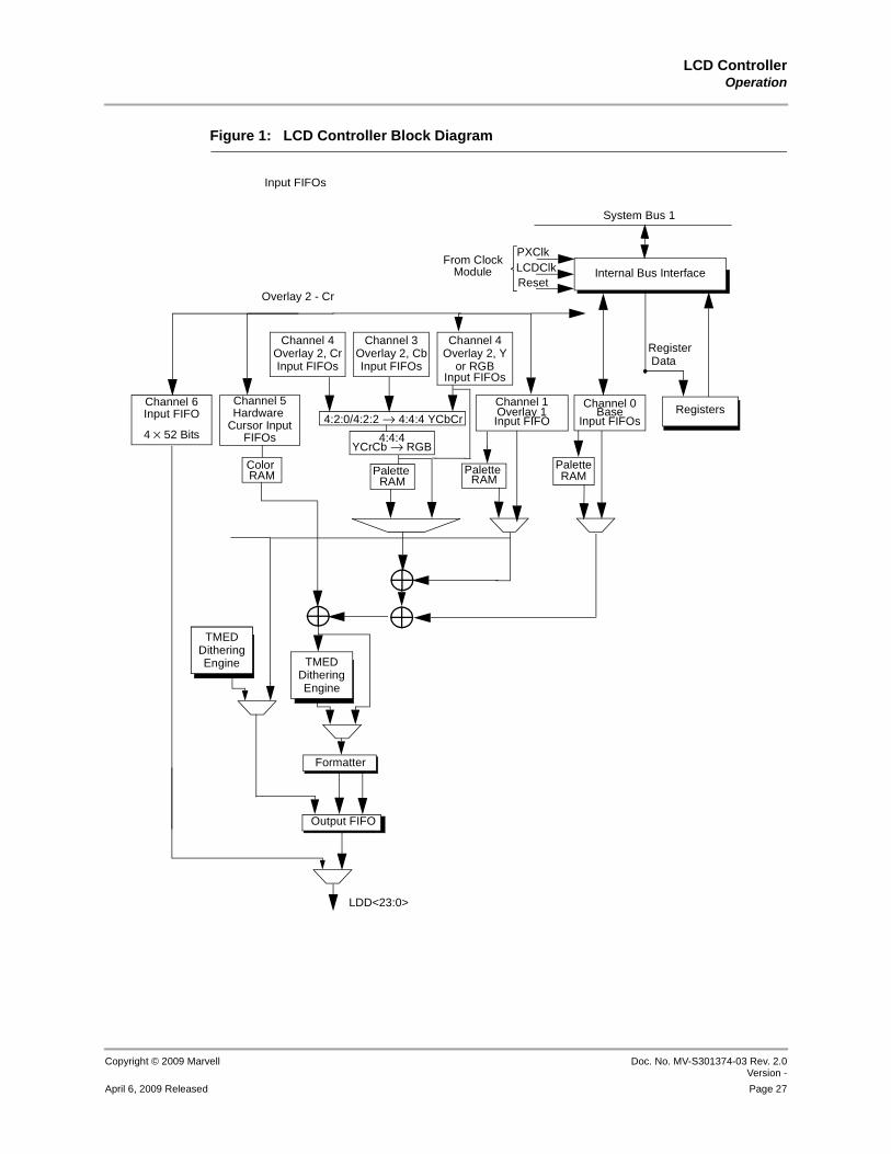
LCD ControllerOperation
Copyright © 2009 Marvell Doc. No. MV-S301374-03 Rev. 2.0Version -
April 6, 2009 Released Page 27
12345678910111213141516171819202122232425262728293031323334353637383940414243444546474849505152535455565758
Figure 1: LCD Controller Block Diagram
Internal Bus Interface
Registers
Palette
Output FIFO
Formatter
From ClockModule
PXClkLCDClkReset
Register
Base
Overlay 2 - Cr
Overlay 1Hardware Input FIFOs
Input FIFOs
Palette Palette
YCrCb → RGB
Channel 0Channel 6
Channel 4
Channel 1Channel 5
TMED
Input FIFO
Color
4:4:4
4:2:0/4:2:2 → 4:4:4 YCbCr
RAM RAM RAM RAM
Input FIFO
4 × 52 Bits
System Bus 1
LDD<23:0>
Data
Cursor InputFIFOs
Overlay 2, CrInput FIFOs
Channel 3Overlay 2, CbInput FIFOs
Channel 4Overlay 2, Y
Input FIFOsor RGB
DitheringEngine TMED
DitheringEngine
TMEDDitheringEngine

PXA3xx (88AP3xx) Processor FamilyVolume III: Graphics and Input Controller Configuration Developers Manual
Doc. No. MV-S301374-03 Rev. 2.0 Version -
Copyright © 2009 Marvell
Page 28 April 6, 2009 Released
12345678910111213141516171819202122232425262728293031323334353637383940414243444546474849505152535455565758
The frame and the palette data for the base and overlay planes are fetched by DMA channels (0–4) over the internal system bus into separate dedicated 16 × 64-bit input FIFOs. Each of the base and Overlay 1 planes has a single dedicated FIFO and support pseudo-color as well as several standard RGB formats. The Overlay 2 plane uses three input FIFOs and accepts both RGB and YCbCr formats. The frame and palette data can be stored either in internal SRAM or external memory.
The LCD controller supports mapping frame data to palette entries for 8 bpp formats. For pixel depths greater than 8 bpp, enabling overlays bypasses the palette RAM and combines each of the red, green, and blue color components appropriately. The palette RAM maps the 8 bpp format to 16- or 25-bit values. Three separate 256 × 25-bit palette RAMs are associated with the base, Overlay 1, and Overlay 2 planes.
The data for the base, Overlay 1, Overlay 2, and cursor combine to go through the dither engine for passive displays or directly to the output FIFO for active displays. The data output from the dither logic is grouped into the selected format, such as 8-bit color or 16-bit color, and placed into the output FIFO. The data from the output FIFO is driven onto the LCD data pins.
Eight modes of hardware cursor formats are described in Section 1.4.10. The pixel data for the cursor is fetched from internal SRAM or external memory by DMA Channel 5 over the internal system bus into its associated 16 × 64-bit input FIFO. The pixel data indexes into a 4 × 24-bit color RAM (a small palette) to get 24-bit pixel color. The color RAM holds the 24-bit colors used by the cursor and can be optionally loaded for each frame.
The LCD controller supports LCD panels with internal frame buffers. The command data RAM holds the commands to be sent at the beginning of each frame. The 4 × 52-bit command FIFO is loaded from internal SRAM or external memory by DMA Channel 6 over the internal system bus.
Depending on the type of panel used, the LCD controller is programmed to use 8-, 16-, or 18-bit output-data pins. Single-scan, passive-color displays use 8 pins, and the LCD controller outputs 2 2/3 pixels each pixel clock (8 pins/3 colors/pixel = 2 2/3 pixels per clock). Single-scan, active-color displays use 8, 16, or 18 output-data pins, and the LCD controller outputs 1 pixel each pixel clock. Figure 2 shows why 2 2/3 pixels/each pixel clock are sent with passive displays and 1 pixel/pixel_clock is sent for active displays.
Table 3: DMA Channel Use
Channel No. Comments
0 Fetches frame and the palette data from memory for the base frame
1 Fetches frame and the palette data from memory for Overlay 1
2, 3, 4 Fetches frame and the palette data from memory for Overlay 2
5 Fetches pixel and color RAM data from memory for hardware cursor
6 Fetches command data from the memory for command RAM

LCD ControllerOperation
Copyright © 2009 Marvell Doc. No. MV-S301374-03 Rev. 2.0Version -
April 6, 2009 Released Page 29
12345678910111213141516171819202122232425262728293031323334353637383940414243444546474849505152535455565758
Figure 2: LCD Outputs for Active and Passive Displays
Displays with an internal frame buffer are always driven with eight output data pins, with the data for the color data of one pixel driven each cycle of L_PCLK_WR.
1.4.1.1 Temporal Modulated Energy Distribution (TMED) DitheringTemporal-modulated energy-distribution (TMED) is a method used only with passive panels to create the high-quality dithering required for passive panels. The TMED dithering engine is a portion of the LCD controller as shown in Figure 1. For passive displays, entries selected from the lookup palette (or directly from memory for all pixel depths greater than 8 bits per pixel) are sent to the TMED dithering engine. TMED is a form of temporal dithering; pixels are run through an algorithm to determine whether the pixel should be on or off (modulated over time). See Figure 3 for a high-level diagram.
8-Bit Passive Display 16-Bit Active Display
LDD7
LDD6
LDD5
LDD4
LDD3
LDD2
LDD1
LDD0
2/3 of Pixel 7, P
ixel 8, Pixel 9
Pixel 10, P
ixel 11, 2/3 of Pixel 12
1/3 of Pixel 3, P
ixel 4, Pixel 5, 1/3 P
ixel 6
Pixel 0, P
ixel 1, 2/3 of Pixel 3
LDD15
LDD14
LDD13
LDD12
LDD11
LDD10
LDD9
LDD8
LDD7
LDD6
LDD5
LDD4
LDD3
LDD2
LDD1
LDD0
Pixel 13
Pixel 12
Pixel 11
Pixel 10
R4
R3
R2
R1
R0
G5
G3
G2
G1
G0
B4
B3
B2
B1
B0
G4
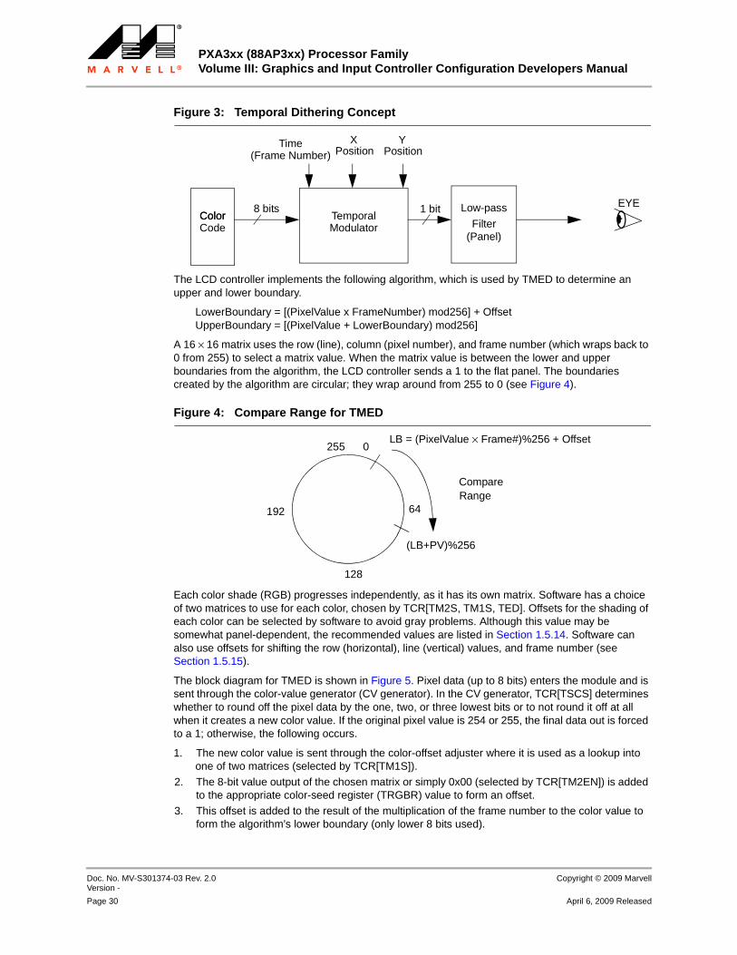
PXA3xx (88AP3xx) Processor FamilyVolume III: Graphics and Input Controller Configuration Developers Manual
Doc. No. MV-S301374-03 Rev. 2.0 Version -
Copyright © 2009 Marvell
Page 30 April 6, 2009 Released
12345678910111213141516171819202122232425262728293031323334353637383940414243444546474849505152535455565758
Figure 3: Temporal Dithering Concept
The LCD controller implements the following algorithm, which is used by TMED to determine an upper and lower boundary.
LowerBoundary = [(PixelValue x FrameNumber) mod256] + OffsetUpperBoundary = [(PixelValue + LowerBoundary) mod256]
A 16 × 16 matrix uses the row (line), column (pixel number), and frame number (which wraps back to 0 from 255) to select a matrix value. When the matrix value is between the lower and upper boundaries from the algorithm, the LCD controller sends a 1 to the flat panel. The boundaries created by the algorithm are circular; they wrap around from 255 to 0 (see Figure 4).
Figure 4: Compare Range for TMED
Each color shade (RGB) progresses independently, as it has its own matrix. Software has a choice of two matrices to use for each color, chosen by TCR[TM2S, TM1S, TED]. Offsets for the shading of each color can be selected by software to avoid gray problems. Although this value may be somewhat panel-dependent, the recommended values are listed in Section 1.5.14. Software can also use offsets for shifting the row (horizontal), line (vertical) values, and frame number (see Section 1.5.15).
The block diagram for TMED is shown in Figure 5. Pixel data (up to 8 bits) enters the module and is sent through the color-value generator (CV generator). In the CV generator, TCR[TSCS] determines whether to round off the pixel data by the one, two, or three lowest bits or to not round it off at all when it creates a new color value. If the original pixel value is 254 or 255, the final data out is forced to a 1; otherwise, the following occurs.
1. The new color value is sent through the color-offset adjuster where it is used as a lookup into one of two matrices (selected by TCR[TM1S]).
2. The 8-bit value output of the chosen matrix or simply 0x00 (selected by TCR[TM2EN]) is added to the appropriate color-seed register (TRGBR) value to form an offset.
3. This offset is added to the result of the multiplication of the frame number to the color value to form the algorithm’s lower boundary (only lower 8 bits used).
EYEColorCode
TemporalModulator
Low-pass
Filter(Panel)
1 bit8 bits
Y X Position Position
Time(Frame Number)
Color
0255
128
192 64
CompareRange
(LB+PV)%256
LB = (PixelValue × Frame#)%256 + Offset

LCD ControllerOperation
Copyright © 2009 Marvell Doc. No. MV-S301374-03 Rev. 2.0Version -
April 6, 2009 Released Page 31
12345678910111213141516171819202122232425262728293031323334353637383940414243444546474849505152535455565758
4. The color value is added to the lower boundary to obtain the upper boundary.5. Row (line) and column (pixel) counters are combined with beat suppression (offset) values in
the pixel number adjuster and address generator to form yet another address for a matrix lookup. TCR[TED] chooses which matrix to use.
6. The output of the chosen matrix is then compared to the lower and upper boundaries in the data generator. If the matrix output is between those boundaries or the original pixel value is 254 or 255, then the data output sent to the panel is a 1, otherwise it is a 0.
Figure 5: TMED Block Diagram
1.4.1.2 Input FIFOsAs shown in Figure 1, there are seven input FIFOs:
One 16 × 64-bit FIFO for the base layer
One 16 × 64-bit FIFO for Overlay 1Three 16 × 64-bit FIFOs for Overlay 2One 16 × 64-bit FIFO for the cursor
One 4 × 64-bit FIFO for the command RAM
Frame data is fetched from the frame buffer by the dedicated LCD DMA controller and is placed in one of seven input FIFO buffers in the LCD controller. Palette data is loaded optionally at the
Lower Boundary
LB =FN x CV + Offset
Generator
FrameCounter
Upper Boundary
UB =LB + CV
Generator
Color ValueGenerator
ColorOffsetAdjuster
DataGenerator
LB > ME > UBor Pixel > 253
Single Color Component Path (GREEN)
Single Color Component Path (BLUE)
Single Color Component Path (RED)
OutputDataBit
FrameNumberAdjuster
FN
CV
LB
UB
LB
OutputDataBit
OutputDataBit
Line Counter Pixel NumberAdjustor
AddressGenerator Matrix
Pixel Counter
frame_clk
line clk
pixel clk
TCR is the TMED Control register
TCR[13:12]
PixelData
TCR[1]
TCR[0]TCR[2]
TSR is the TMED Seed register
TSR[7:0]
TCR[3]
TCR[14]TCR[11:8]
TCR[7:4]
Force to 1
ME

PXA3xx (88AP3xx) Processor FamilyVolume III: Graphics and Input Controller Configuration Developers Manual
Doc. No. MV-S301374-03 Rev. 2.0 Version -
Copyright © 2009 Marvell
Page 32 April 6, 2009 Released
12345678910111213141516171819202122232425262728293031323334353637383940414243444546474849505152535455565758
beginning of each frame. This data is written to the internal palette RAM at the output of the FIFO. Following the palette fetch, the first FIFO is filled with encoded pixels and pixel processing begins.
The FIFO signals a service request to the DMA whenever four entries of the FIFO are empty. Pixel data remains packed within individual 64-bit words when it is loaded into the FIFO. The LCD controller port size is 64 bits wide to accommodate the heavy data flow from the frame buffer. If the pixel size is 8 bits, the FIFO entries are unpacked and used to index the palette RAM to read the color value. For 16-, 18-, 19-, 24-, or 25-bit pixels, if passive, the entries bypass the palette and go directly to the TMED dither logic. In active (TFT) mode, the pixels are output directly to the pins.
1.4.1.3 Lookup PaletteEight-bit pixel encodings select any of the 256 palette entries. The palette RAM is bypassed for pixel depth greater than 8 bpp. When 16-bit data is used without transparency, the color palette RAM for the base is 16-bit wide × 256 locations. For all other combinations using palettes, the color palette RAMs for base and overlays are each 25-bits wide × 256 locations. Depending on the value of the LCCR4[PAL_FOR] bit, 16, 18, or 24 bits of the data is used according to the data width (number of bits per pixel). Bit 25 defines the transparency of the pixel. The encoded pixel data taken from the bottom entry of the channel input FIFO is used as an address to index and select individual palette locations. or details on LCCR4[PAL_FOR], see Table 46, “LCCR4 Bit Definitions,” on page 98.
1.4.1.4 Output FIFOThe LCD controller contains a 64-entry × 24-bit-wide output FIFO that is used to store pixel pin data before it is driven out to the pins. Each time a modulated pixel value is output from the dither generator, it is placed into a serial shifter. The size of the shifter is controlled by programming the passive/active select bit in the LCD Control registers, and the pixel bit size in the frame Descriptor in memory. The shifter can be configured to be 8, 16, 18, or 24 bits wide. Once the correct number of pixels has been placed within the shifter (8-, 16-, 18-, or 24-bit pixel values), the value is transferred to the top of the output FIFO. The value is then transferred down until it reaches the last empty location within the FIFO. Each time a value is taken from the bottom of the FIFO, the entry is invalidated and all data in the FIFO moves down one position.
1.4.2 Pixel Clock Frequency CalculationFor passive and active displays, the pixel-clock divider field (LCCR3[PCD]) is used along with the PCD divisor select (LCCR4[PCDDIV]) to configure the frequency of the pixel clock. LCCR3[PCD] can be any value from 0 to 255 and is used to generate a range of pixel-clock frequencies from LCLK/2 to LCLK/512, where LCLK is the programmed frequency of the LCD controller/system bus frequency. LCLK can vary from 104.0 MHz to 208.0 MHz for normal D0 mode operation.
The pixel-clock frequency is adjusted to meet the required screen-refresh rate, which depends on several factors:
The number of pixels for the target displayThe number of pixel-clock wait states programmed at the beginning and end of each line
The number of line clocks inserted at the beginning and end of each frameThe width of the VSYNC signal in active mode or VSW line clocks inserted in passive modeThe width of the frame clock or HSYNC signal
All of these factors alter the duration between frame transmissions. Different display manufacturers require different frame-refresh rates, depending on the physical characteristics of the display. LCCR3[PCD] and LCCR4[PCDDIV] alter the pixel-clock frequency to meet these requirements.
If LCCR4[PCDDIV] is cleared, the frequency of the pixel clock for a set pixel-clock divider value or the required LCCR3[PCD] value to yield a target pixel-clock frequency can be calculated using the following two equations:

LCD ControllerOperation
Copyright © 2009 Marvell Doc. No. MV-S301374-03 Rev. 2.0Version -
April 6, 2009 Released Page 33
12345678910111213141516171819202122232425262728293031323334353637383940414243444546474849505152535455565758
If LCCR4[PCDDIV] is set, the frequency of the pixel clock for a set pixel-clock divider value or the required LCCR3[PCD] value to yield a target pixel-clock frequency can be calculated using the following two equations:
For LCD panels with an internal frame buffer, the PCD field is used to specify the command-inhibit time between two consecutive Write accesses to the LCD panel. The command-inhibit time is equal to:
(LCCR3[PCD]+1)*LCD_CLK_PERIOD
1.4.3 Bandwidth Calculations The equations in this section provide a way to estimate the LCD bandwidth needed to drive an LCD panel with the PXA3xx processor. LCD bandwidth can affect overall system performance by reducing the available system memory bus bandwidth. The LCD controller can be programmed with timing values that control the refresh rate and the needed LCD bandwidth for a specific LCD panel. The total needed memory bus bandwidth can be defined as the LCD bandwidth plus the system memory bus bandwidth used by any other running processes in the processor. When the total memory bus bandwidth needed exceeds the total available memory bus bandwidth, visible video artifacts may be seen on the LCD panel.
The number of pixel clocks to send one line of pixels is calculated using the following equation:
Or:
where:
HSW = Horizontal Sync Width
PixelClockFrequency LCLK2 PCD 1+( )------------------------------=
PCD LCLK2 PixelClockFrequency( )---------------------------------------------------------------------- 1–=
PixelClockFrequency LCLKPCD 1+( )
---------------------------=
PCD LCLKPixelClockFrequency( )
------------------------------------------------------------------- 1–=
Total Needed Memory Bus Bandwidth LCD Bandwidth System Memory Bus Bandwidth+=
PixelClocksLine
---------------------------------- HSW 1+( ) BLW 1+( ) PPL 1+( ) ELW 1+( )+ + +=
PixelClocksLine
---------------------------------- HSW BLW PPL ELW 4+ + + +=

PXA3xx (88AP3xx) Processor FamilyVolume III: Graphics and Input Controller Configuration Developers Manual
Doc. No. MV-S301374-03 Rev. 2.0 Version -
Copyright © 2009 Marvell
Page 34 April 6, 2009 Released
12345678910111213141516171819202122232425262728293031323334353637383940414243444546474849505152535455565758
BLW = Beginning of Line WidthPPL = Pixels Per Line (Frame width -1)
ELW = End of Line width
The number of line clocks (HSYNC clocks) needed to send one frame is calculated using the following equation:
Or:
where:
VSW = Vertical Sync WidthBFW = Beginning of Frame WidthLPP = Lines Per Page (Frame height -1)
EFW = End of Frame Width
The number of pixel clocks to send one frame is calculated using the following equation:
substituting:
Because LPP = Height – 1 and PPL = Width – 1, the following equation applies:
The refresh rate, which is the number of frames per second that the LCD controller is fetching from memory and sending to the LCD panel, can be calculated using the following equation:
The LCD data rate required for each plane to support the LCD panel selected for the system is calculated using this formula:
LineClocksFrame
-------------------------------- VSW 1+( ) BFW LPP 1+( ) EFW+ + +=
LineClocksFrame
-------------------------------- VSW BFW LPP EFW 2+ + + +=
PixelClocksFrame
---------------------------------- LineClocksFrame
-------------------------------- PixelClocksLine
----------------------------------×=
PixelClocksFrame
---------------------------------- VSW BFW LPP EFW 2+ + + +( ) HSW BLW ELW PPL 4+ + + +( )×=
PixelClocksFrame
---------------------------------- VSW BFW Height EFW 1+ + + +( ) HSW BLW ELW Width 3+ + + +( )×=
Data Rate Length Width Refresh Rate Bits per Pixel×××8
----------------------------------------------------------------------------------------------------------------------------⎝ ⎠⎛ ⎞bps=

LCD ControllerOperation
Copyright © 2009 Marvell Doc. No. MV-S301374-03 Rev. 2.0Version -
April 6, 2009 Released Page 35
12345678910111213141516171819202122232425262728293031323334353637383940414243444546474849505152535455565758
The bits per pixel is the number of bits used in the memory to store each pixel, for example 16 bits for a pixel depth of 16 bpp, 32 bits for a pixel depth of 18 bpp unpacked, and 24 bits for a pixel depth of 18 bpp packed. See Section 1.4.12, Frame Buffer to derive the bits-per-pixel value.
The number of 4-beat burst operations (8 bytes/beat) that are generated by the LCD DMA controller is as follows:
The time consumed by the LCD refresh operation is then calculated by:
The value of Pdma is the period in microseconds of LCD DMA four-beat burst, including SDRAM precharge time. The time remaining within each second after deducting the LCD refresh time is the time available for instruction and data fetches, hardware accesses, and memory refresh operations. Use caution when setting system parameters, such as core frequency, system frequency, memory frequency, and bus arbiter settings to ensure that LCD FIFOs do not underrun due to bus latencies caused by other internal and external peripherals. This caution applies especially for interrupt and polled modes that require a longer time to service.
1.4.4 Graphical OverlaysThe LCD controller supports a base plane plus two overlays and hardware cursor. Figure 6 shows the display of hardware cursor, base frame, and two overlays on the LCD panel.
Refresh Rate PixelClockFrequencyPixelClocks
Frame----------------------------------⎝ ⎠⎛ ⎞
--------------------------------------------------------------=
LCD DMA burst Count Data Rate32
---------------------------⎝ ⎠⎛ ⎞ Burst/sec=
LCD refresh time LCD DMA burst count Pdma×( ) / second=

PXA3xx (88AP3xx) Processor FamilyVolume III: Graphics and Input Controller Configuration Developers Manual
Doc. No. MV-S301374-03 Rev. 2.0 Version -
Copyright © 2009 Marvell
Page 36 April 6, 2009 Released
12345678910111213141516171819202122232425262728293031323334353637383940414243444546474849505152535455565758
Figure 6: Hardware Cursor, Base Plus 2 Overlays Displayed on LCD Panel
The display order of the cursor, base frame, and overlays is shown in Table 4.
Overlay 2
Overlay 1
LCD Panel
Cursor
Base Frame
cursorOverlay 1Overlay 2 Cursor
The dashed areas of the overlays demonstrate the position and size of the base plane. The dashed areas are not defined in the overlay frame buffers in this example.
Base Frame
Table 4: Display Order of Three Layers and Cursor on LCD Panel
Layer Number Plane
LCCR0[OUC] = 0b0:
TOP or 1st Hardware Cursor
Second Base Plane
Third Overlay 1 Window
Fourth Overlay 2 Window
LCCR0[OUC] = 0b1:
TOP or 1 Hardware Cursor
2 Overlay 1 Window
3 Overlay 2 Window
4 Base Plane
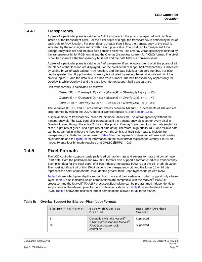
LCD ControllerOperation
Copyright © 2009 Marvell Doc. No. MV-S301374-03 Rev. 2.0Version -
April 6, 2009 Released Page 37
12345678910111213141516171819202122232425262728293031323334353637383940414243444546474849505152535455565758
1.4.4.1 TransparencyA pixel of a particular plane is said to be fully transparent if the pixel in a layer below it displays instead of the transparent pixel. For the pixel depth of 8 bpp, the transparency is defined by bit 25 of each palette RAM location. For pixel depths greater than 8 bpp, the transparency of the pixel is indicated by the most significant bit within each pixel value. The pixel is fully transparent if the transparency bit is set and the data field contains all zeros. The Overlay 2 transparency is defined by the transparency bit for RGB format and the Overlay 2 is not transparent for YCbCr format. The pixel is half transparent if the transparency bit is set and the data field is a non-zero value.
A pixel of a particular plane is said to be half transparent if some logical blend of all the pixels of all the planes at that location are displayed. For the pixel depth of 8 bpp, half-transparency is indicated by setting bit 25 of each palette RAM location, and the data field is a non-zero number. For pixel depths greater than 8bpp, half-transparency is indicated by setting the most significant bit of the pixel to logical 1, and the data field is a non-zero number. The half-transparency applies only for Overlay 1, while Overlay 2 and the base layer do not support half-transparency.
Half-transparency is calculated as follows:
The variables K1, K2, and K3 are constant values between 1/8 and 1 in increments of 1/8, and are programmed by writing the LCD Controller Control register 4. See Section 1.5.5.
A special mode of transparency, called 24-bit mode, allows the use of transparency without the transparency bit. The LCD controller operates as if the transparency bit is set for every pixel in Overlay 1, even though the entire 24 bits of the pixel in Overlay 1 are used for color data (eight bits of red, eight bits of green, and eight bits of blue data). Therefore, high quality RGB and YCbCr data can be streamed in without the need to convert the 24 bits of RGB color data to include the transparency bit. Refer to the last row of Table 6 for the required combination of base and overlay pixel formats and to Figure 29 for information on the pixel format required for Overlay 1 in 24-bit mode. Twenty-four-bit mode requires that OVL1C1[BPP1] = 0x0.
1.4.5 Pixel FormatsThe LCD controller supports basic pelletized bitmap formats and several formats that contain raw RGB data. Both the pelletized and raw RGB formats also support a format to indicate transparency. Each pixel data for the pixel depth of 8-bpp indexes into palette RAM to get the 16- or 25-bit value. The most significant bit of this 25-bit value is the transparency bit, and the lower 16 or 24 bits represent the color components. Pixel depths greater than 8-bpp bypass the palette RAM.
Table 5 shows which pixel depths support both base and the overlays and which support only a base layer. Table 5 also indicates which combinations are compatible with the Marvell® PXA25x processor and the Marvell® PXA26x processor.Each plane can be programmed independently to support one of the allowed pixel format combinations shown in Table 6, when the data format is RGB. Table 6 shows the bits/pixel format combinations allowed for all three planes.
Output R( ) Overlay1 R( ) K1× Base R( ) Overlay2 R( )+( ) 1 K1–( )×+=
Output G( ) Overlay1 G( ) K2× Base G( ) Overlay2 G( )+( ) 1 K2–( )×+=
Output B( ) Overlay1 B( ) K3× Base B( ) Overlay2 B( )+( ) 1 K3–( )×+=
Table 5: Overlay Support for Bits-per-Pixel (bpp) Formats
Bits-per-Pixel Format Base with Overlays Disabled
Base with Overlays Enabled
8 Compatible with the Marvell® PXA25x processor and Marvell® PXA26x processor LCD controllers.
Supported
16 Supported

PXA3xx (88AP3xx) Processor FamilyVolume III: Graphics and Input Controller Configuration Developers Manual
Doc. No. MV-S301374-03 Rev. 2.0 Version -
Copyright © 2009 Marvell
Page 38 April 6, 2009 Released
12345678910111213141516171819202122232425262728293031323334353637383940414243444546474849505152535455565758
The LCD controller also supports 4:2:0, 4:2:2 and 4:4:4 YCbCr video sampling formats for the Overlay 2 plane. The color space conversion from YCbCr to RGB is performed based on the ITU-R BT.601 standard (previously known as CCIR 601). The YCbCr formats supported are provided in Table 7.
16 (RGB565 with chroma keying enabled)
Supported Supported
18 Supported Not Supported
19 Not Supported Supported
24 Supported Supported
25 Not Supported Supported
Table 6: Bits-per-Pixel Format Combinations Allowed
Base Overlay 1 Overlay 2 Resultant RGB Value
8 8 or width of base palette 8 or width of base palette or YCbCr
Width of the palettes defined
16 8 or 16 8, 16 or YCbCr 16 bits
16(RGB5:6:5 with chroma-keying enabled)
16 (RGB5:6:5 with chroma-keying enabled)
16 (RGB5:6:5 with chroma-keying enabled) or YCbCr
16 bits
18 8 or 18 8, 18 or YCbCr 18 bits
19 8 or 19 8, 19 or YCbCr 18 bits
19 16 (RGB5:6:5 with chroma-keying enabled)
16 (RGB5:6:5 with chroma-keying enabled) or YCbCr
18 bits
24 8 or 24 8, 24 or YCbCr 24 bits
25 8 or 25 8, 25 or YCbCr 24 bits
16 RGBT 24-bit mode1 24-bit YCbCr 16 bits for panels without internal frame buffers.2
24 bits for panels with internal frame buffers
1 Refer to Section 1.4.4.1 for a description of this mode.2 Refer to Section 1.4.8.3 for a description of the method of conversion from 24 bits to 16 bits.
Table 5: Overlay Support for Bits-per-Pixel (bpp) Formats (Continued)
Bits-per-Pixel Format Base with Overlays Disabled
Base with Overlays Enabled

LCD ControllerOperation
Copyright © 2009 Marvell Doc. No. MV-S301374-03 Rev. 2.0Version -
April 6, 2009 Released Page 39
12345678910111213141516171819202122232425262728293031323334353637383940414243444546474849505152535455565758
Table 8 shows the valid pixel formats for each base/overlay frame.
LCCR3[PDFOR] and LCCR4[PAL_FOR] are used to configure the pixel formats for the base layer. PDFOR configures the pixel data format that the LCD frame buffer represents for all pixel formats of 16 bpp or larger. Not all values of PDFOR are valid for all pixel depths. Valid selections are specified in Section 1.5.4, LCD Controller Control Register 3 (LCCR3), on page 90 and Section 1.5.5, LCD Controller Control Register 4 (LCCR4), on page 97.
A palette is required for pixel depths less than 16 bpp. PAL_FOR configures the palette format for the base plane. Four formats are possible. Refer to Table 46 and Section 1.4.11.1 for details on configuring the palette. Table 9 shows the valid PAL_FOR and PD_FOR for various base pixel formats.
Table 7: Video Sampling Formats Supported by Overlay 2
YCbCr Format
Comments
4:4:4 The color space conversion from 4:4:4 YCbCr to RGB 8:8:8
4:2:2 Video data in 4:2:2 format is converted to 4:4:4 prior to color space conversion to RGB 8:8:8. OVL2C1[PPL2] must be > 1
4:2:0 Video data in 4:2:0 format is converted to 4:4:4 prior to color space conversion to RGB 8:8:8. OVL2C1[PLL2] must be > 1 and OVL2C1[LPO2] must be > 1
Table 8: Valid Pixel Formats for Each Frame
Frame Valid bpp: Overlays Enabled Valid bpp: Overlays Disabled
Base 8, 16, 19, 24, 25 8, 16, 18, 24
Overlay1 8, 16, 19, 24, 25, 24-bit mode NA
Overlay2 8,16,19,24,25 YCbCr4:4:4, YCbCr4:2:2, YCbCr4:2:0 NA
Table 9: Valid Combinations of PDFOR and PAL_FOR for Various Base bpp
Base bpp
PAL_FOR PDFOR with Overlays Enabled
PDFOR with Overlays Disabled
Notes
8 0b00 NA 0b00 For 16 bpp panels. No transparency
8 0b01 0b11 NA For 16 bpp panels.Transparency required
8 0b10 0b00†
LCCR3[BPP] = 0x7 or 0x8
0b11LCCR3[BPP] = 0x5 or 0x6
For 18 bpp panels.Transparency optional.
8†† 0b11 0b00†
LCCR3[BPP] = 0xA0b11LCCR3[BPP] = 0x9
For smart panels.Transparency optional
16 0b00† 0b11 0b00 For 16 bpp panels.Transparency optional

PXA3xx (88AP3xx) Processor FamilyVolume III: Graphics and Input Controller Configuration Developers Manual
Doc. No. MV-S301374-03 Rev. 2.0 Version -
Copyright © 2009 Marvell
Page 40 April 6, 2009 Released
12345678910111213141516171819202122232425262728293031323334353637383940414243444546474849505152535455565758
Note
Note The value of PDFOR is ignored for pixel depths where only one RGB format is possible (19 bpp and 25 bpp).
1.4.5.1 Data Format for Pixel Depths of 8 bppThe palette RAM (internal to the LCD controller) is for mapping the 8-bpp formats to a color value defined by the palette. See Section 1.4.11.1 for details on the format of the data in the palette buffer. The palette RAM must be loaded at least once before the pixel data can be displayed on the LCD panel. The palette RAM is loaded from the palette buffer, which is a separate, small frame buffer used for the palette. Figure 10 describes the number of entries and formats for the possible pelletized formats.
If transparency is used, the most significant bit determines the transparency and the lower 24 bits represent the red, green, and blue color components. Load the palette RAM so that Bit 25 of each location defines transparency. Ensure that bit 25 bit is cleared to 0 if transparency is not intended. Figure 16 details the format of the pixel data when overlays are used.
16 0b00† 0b00 NA For 16 bpp panels with chroma-keying enabled for Overlay 1 or Overlay 2. Base plane chroma-keying enabled/disabled or base plane set for constant color
18 0b00† NA 0b11 For 18 bpp panels.No transparency
19 0b00† 0b00† NA For 18 bpp panels.Transparency required
24 0b00† 0b10 0b11 For smart panels.Transparency optional24-bpp panel support also in PXA31x
25 0b00† 0b00† NA For smart panels.Transparency required24-bpp panel support also in PXA31x
NOTES:
† Indicates that the value of this field is ignored for this mode. The use of the reset value of 0b00 is recommended; however, any value is acceptable.
†† PAL_FOR cannot be 3 if LCCR0[LCDT]is clear and LCCR0[PAS] is set.
Note: If a palette is used for the base plane, the pixel data in the frame buffer format is that shown in Figure 15 through Figure 18 (not the format specified by PDFOR).
Table 9: Valid Combinations of PDFOR and PAL_FOR for Various Base bpp (Continued)
Base bpp
PAL_FOR PDFOR with Overlays Enabled
PDFOR with Overlays Disabled
Notes

LCD ControllerOperation
Copyright © 2009 Marvell Doc. No. MV-S301374-03 Rev. 2.0Version -
April 6, 2009 Released Page 41
12345678910111213141516171819202122232425262728293031323334353637383940414243444546474849505152535455565758
.
1.4.5.2 Data Format for RGB Color SpaceThe LCD controller supports several standard pixel depths for the RGB color space. Pixel depth corresponds to the total number of bits required for representing the red, green, and blue color components with a transparency bit, if applicable. When the overlays are disabled, the pixel depth corresponds directly to the number of bits used to represent the color components. When the overlays are enabled, the most significant bit is used to indicate transparency. The two formats are referred to as RGB and RGBT, respectively, with the integer fields representing the number of bits used to represent each color channel. The supported RGB and RGBT formats are listed in Table 11; all combinations of the overlays allowed are listed in Table 6, “Bits-per-Pixel Format Combinations Allowed,” on page 38.
Data Format for Pixel Depth of 16 Bits-per-PixelThe 16-bpp format supports two modes. In the first mode, the overlays are disabled and a true 16- bpp format (which supports 65536 possible colors) is provided. The second mode is used when the overlays are enabled. In this mode, the most significant bit indicates transparency, with the remaining 15 bits used for the color components.
One format is supported with the overlay planes disabled, RGB 5:6:5 as illustrated in Table 12. The format is selected by setting the PDFOR bit field for the base, Overlay 1, and Overlay 2 planes as described in Section 1.5. P
Table 10: Palette Entries for 8 bpp Format
Pel let izedFormat
Palette Entries
Comments
8 bpp 256 Transparency supported if overlays enabled, at 16 bpp, 18 bpp, 19 bpp, 24 bpp, and 25 bpp.
Table 11: Standard RGB and RGBT Formats
Memory Depth
RGB Formats: Overlays Disabled
RGB Formats: Overlays Enabled
16 bits RGB 5:6:5 RGBT 5:5:5 or RGB 5:6:5 with chroma-key enabled
18 bits RGB 6:6:6 NA
19 bits NA RGBT 6:6:6
24 bits RGB 8:8:8 RGBT 8:8:7, RGB 8:8:81
25 bits NA RGBT 8:8:8
1 RGB 8:8:8 is called 24-bit mode and is possible only with Overlay 1.
Table 12: Pixel Depth of 16 Bits-per-Pixel with Overlays Disabled
Bit 15 14 13 12 11 10 9 8 7 6 5 4 3 2 1 0
PDFOR 00format1
Red [4:0] Green [5:0] Blue [4:0]

PXA3xx (88AP3xx) Processor FamilyVolume III: Graphics and Input Controller Configuration Developers Manual
Doc. No. MV-S301374-03 Rev. 2.0 Version -
Copyright © 2009 Marvell
Page 42 April 6, 2009 Released
12345678910111213141516171819202122232425262728293031323334353637383940414243444546474849505152535455565758
The RGBT 5:5:5 format is provided when one or both of the overlays are enabled. Each of the color components uses five bits with the most significant bit in the 16-bit word specifying transparency. The RGBT 5:5:5 format is illustrated in Table 13.
Data Format for Pixel Depth of 16 Bits-per-Pixel with Overlays and Chroma-Keying EnabledFor PXA31x only, one format is supported with the overlay planes and chroma-keying enabled, RGB 5:6:5 as illustrated in Table 14. The LCCR4[CHRM_SEL] bit selects a particular pixel color to use as transparency color for base/overlays. The LCCR4[OV2_CHRM_EN] bit enables use of a particular pixel color as the transparency color for Overlay 2. See Table 46, “LCCR4 Bit Definitions,” on page 98.
Supported overlay and chroma-keying configurations are:
Overlay 1 enabled with Overlay 1 chroma-keying enabled.Overlay 2 enabled with Overlay 2 chroma-keying enabled.
Base plane chroma-keying enabled/disabled or base plane set for constant color.
For PXA31x only, the format is selected by setting the PDFOR bit field for the base, Overlay 1, and Overlay 2 planes as described in Section 1.5. P
Data Format for Pixel Depth of 18 Bits-per-PixelThe 18-bpp format is used when both overlays are disabled. The 18 bits allow 262,144 possible colors with six bits each of red, green, and blue. The RGB 6:6:6 format is shown in Table 15.
Table 13: Pixel Depth of 16 Bits-per-Pixel with Overlays Enabled
Bit 15 14 13 12 11 10 9 8 7 6 5 4 3 2 1 0
PDFOR 11format4
T Red [4:0] Green [4:0] Blue [4:0]
NOTES:1. When Bit T (pixel data bit 15) is set and pixel data is non-zero, half Transparency mode is enabled.2. When pixel data = 0x8000, full Transparency mode is enabled.
Table 14: PXA31x processor Only: Pixel Depth of 16 Bits with Overlays and Chroma-Keying Enabled
Bit 15 14 13 12 11 10 9 8 7 6 5 4 3 2 1 0
PDFOR 00format1
Red [4:0] Green [5:0] Blue [4:0]
Table 15: Pixel Depth of 18 Bits-per-Pixel with Overlays Disabled
Bit 17 16 15 14 13 12 11 10 9 8 7 6 5 4 3 2 1 0
PDFOR 11format4
Red[5:0] Green[5:0] Blue[5:0]
Table 16: PXA31x processor Only: Pixel Depth of 18 Bits-per-Pixel in (6R+2’0, 6G+2’0, 6B+2’0) Format with Overlays Disabled
Bit 23 22 21 20 19 18 17 16 15 14 13 12 11 10 9 8 7 6 5 4 3 2 1 0
PDFOR is Don’t care
Red[5:0] 0 0 Green[5:0] 0 0 Blue[5:0] 0 0
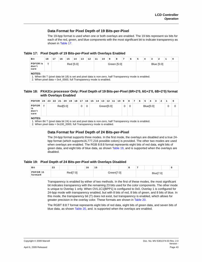
LCD ControllerOperation
Copyright © 2009 Marvell Doc. No. MV-S301374-03 Rev. 2.0Version -
April 6, 2009 Released Page 43
12345678910111213141516171819202122232425262728293031323334353637383940414243444546474849505152535455565758
Data Format for Pixel Depth of 19 Bits-per-PixelThe 19-bpp format is used when one or both overlays are enabled. The 19 bits represent six bits for each of the red, green, and blue components with the most significant bit to indicate transparency as shown in Table 17.
Data Format for Pixel Depth of 24 Bits-per-PixelThe 24-bpp format supports three modes. In the first mode, the overlays are disabled and a true 24- bpp format (which supports16,777,216 possible colors) is provided. The other two modes are used when overlays are enabled. The RGB 8:8:8 format represents eight bits of red data, eight bits of green data, and eight bits of blue data, as shown Table 19, and is supported when the overlays are disabled.
Transparency is enabled by either of two methods. In the first of these modes, the most significant bit indicates transparency with the remaining 23 bits used for the color components. The other mode is unique to Overlay 1 only. When OVL1C1[BPP1] is configured to 0x0, Overlay 1 is configured for 24-bpp mode with transparency enabled, but with 8 bits of red, 8 bits of green, and 8 bits of blue. In this mode, the transparency bit (T) does not exist, but transparency is enabled, which allows for greater precision in the overlay color. These formats are shown in Table 20.
The RGBT 8:8:7 format represents eight bits of red data, eight bits of green data, and seven bits of blue data, as shown Table 20, and. is supported when the overlays are enabled.
Table 17: Pixel Depth of 19 Bits-per-Pixel with Overlays Enabled
Bit 18 17 16 15 14 13 12 11 10 9 8 7 6 5 4 3 2 1 0
PDFOR is don’t care
T Red [5:0] Green [5:0] Blue [5:0]
NOTES:1. When Bit T (pixel data bit 18) is set and pixel data is non-zero, half Transparency mode is enabled.2. When pixel data = 0x4_0000, full Transparency mode is enabled.
Table 18: PXA31x processor Only: Pixel Depth of 19 Bits-per-Pixel (6R+2’0, 6G+2’0, 6B+2’0) format with Overlays Enabled
PDFOR 24 23 22 21 20 19 18 17 16 15 14 13 12 11 10 9 8 7 6 5 4 3 2 1 0
PDFOR is don’t care
T Red[5:0] 0 0 Green[5:0] 0 0 Blue[5:0] 0 0
NOTES:1. When Bit T (pixel data bit 24) is set and pixel data is non-zero, half Transparency mode is enabled.2. When pixel data = 0x100_0000, full Transparency mode is enabled.
Table 19: Pixel Depth of 24 Bits-per-Pixel with Overlays Disabled
Bit 23 16 15 8 7 0
PDFOR 11format4
Red[7:0] Green[7:0] Blue[7:0]

PXA3xx (88AP3xx) Processor FamilyVolume III: Graphics and Input Controller Configuration Developers Manual
Doc. No. MV-S301374-03 Rev. 2.0 Version -
Copyright © 2009 Marvell
Page 44 April 6, 2009 Released
12345678910111213141516171819202122232425262728293031323334353637383940414243444546474849505152535455565758
Data Format for Pixel Depth of 25 Bits-per-PixelThe 25-bpp format is used when one or both of the overlays are enabled. The 25 bits represent eight bits for each of the red, green, and blue components with the most significant bit to indicate transparency as shown in Table 21.
1.4.5.3 Data Format for YCbCr Color SpaceThe YCbCr video sampling format is used in Overlay 2. In this format, luminance information is stored as a single component (Y), and chrominance information is stored as two color-difference components (Cb and Cr). Cb represents the difference between the blue component and a reference value. Cr represents the difference between the red component and a reference value. Y is defined to have a nominal range of 16 to 235; Cb and Cr are defined to have a range of 16 to 240, with zero signal corresponding to level 128.
The LCD controller supports the following three YCbCr video formats:
4:4:4 YCbCr sampling format4:2:0 YCbCr sampling format4:2:2 YCbCr sampling format
4:4:4 YCbCr Video FormatIn 4:4:4 YCbCr video format, in each video frame, the number of samples of each chrominance component, Cr or Cb, is the same as that of the number of samples of luminance, both horizontally and vertically. For instance, for every sample of luminance, two samples of chrominance exist—one a Cr sample and the other a Cb sample. In a frame of 4:4:4 YCbCr video, the locations of chrominance samples is the same as that of luminance samples, as shown in Figure 7.
Table 20: Pixel Depth of 24 Bits-per-Pixel with Overlays Enabled
Bit 23 22 17 16 15 14 8 7 6 0
PDFOR 10format31,2 T Red [7:0] Green [7:0] Blue [6:0]
24 bit mode3 Red [7:0] Green [7:0] Blue [7:0]
NOTES:1. When Bit T (pixel data bit 23) is set and pixel data is non-zero, half Transparency mode is enabled.2. When pixel data = 0x80_0000, full Transparency mode is enabled.3. This format is only available for Overlay 1. The value of PDFOR is ignored for this mode. OVL1C1[BPP1] = 0x0 for this
mode. See Section 1.4.4.1 on page ii-37.
Table 21: Pixel Depth of 25 Bits-per-Pixel with Overlays Enabled
Bit 24 23 16 15 8 7 0
T Red [7:0] Green [7:0] Blue [7:0]
Note:1. When Bit T (pixel data bit 24) is set and pixel data is non-zero, half Transparency mode is enabled.2. When pixel data = 0x100_0000, full Transparency mode is enabled.

LCD ControllerOperation
Copyright © 2009 Marvell Doc. No. MV-S301374-03 Rev. 2.0Version -
April 6, 2009 Released Page 45
12345678910111213141516171819202122232425262728293031323334353637383940414243444546474849505152535455565758
Figure 7: Luminance and Chrominance Samples in 4:4:4 YCbCr Video Frame
The luminance and chrominance values are 8 bits each. The PXA30x and PXA31x processors supports storage of 4:4:4 YCbCr video format in planar or packed format in the frame buffer. The frame buffer can reside in internal SRAM or external memory. In planar format, the luminance and chrominance data are stored in three different regions in the memory. In packed format, the luminance and chrominance data is stored packed in one memory region.
4:2:2 YCbCr FormatIn the 4:2:2 YCbCr video format, in each frame of video, the number of samples per line of each chrominance component, Cr or Cb, is one-half of the number of samples per line of luminance. The chrominance resolution is the same as that of luminance resolution vertically. The exact location of chrominance samples with respect to luminance samples in a frame of 4:2:2 video is shown in Figure 8.
Figure 8: Luminance and Chrominance Samples in 4:2:2 Video Frame
The luminance and chrominance values are 8 bits each. The LCD controller supports the storage of 4:2:2 YCbCr video format in planar format in the frame buffer.
4:2:0 YCbCr FormatIn 4:2:0 YCbCr video format, in each frame of video, the number of samples of each chrominance component, Cr or Cb, is one-half of the number of samples of luminance, both horizontally and vertically. The exact location of chrominance samples with respect to luminance samples in a frame
= Y Sample = Cr and Cb Samples
= Y Sample = Cr or Cb Sample

PXA3xx (88AP3xx) Processor FamilyVolume III: Graphics and Input Controller Configuration Developers Manual
Doc. No. MV-S301374-03 Rev. 2.0 Version -
Copyright © 2009 Marvell
Page 46 April 6, 2009 Released
12345678910111213141516171819202122232425262728293031323334353637383940414243444546474849505152535455565758
of 4:2:0 video is shown in Table 9.The luminance and chrominance values are 8 bits each. The LCD controller supports the storage of 4:2:0 video format in planar format in the frame buffer.
Figure 9: Luminance and Chrominance Samples in 4:2:0 YCbCr Video Frame
1.4.6 Base FrameThe number of pixel elements in the base frame is always equal to the resolution of the screen and can be stored in either internal SRAM or external memory in any of the formats described in Section 1.4.5. The screen coordinates are expressed in pixels, and a left-handed coordinate system is used to reference a spatial location within the screen. The upper left corner of the screen is (0,0), with the X coordinate increasing from left to right and the Y coordinate increasing from top to bottom.
The pixel format is established by writing to the LCD Controller Register 3, as described in Table 44. For pixel depth of 8 bpp, the palette data is loaded into the palette RAM by DMA Channel 0. If the pixel depth is greater than 8 bpp, the pixel data from the input FIFO bypasses the palette RAM.
The palette RAM provides for mapping the 8-bpp format to a 16- or 25-bit value and must be loaded at least once before the pixel data can be displayed on the LCD panel. If transparency is used, the most significant bit determines the transparency, and the lower 24 bits (for color) represent the red, green, and blue color components. The frame data is loaded into its dedicated input FIFO by DMA Channel 0.
1.4.7 Overlay 1 WindowThe number of pixel elements and the position of Overlay 1 are programmable. The pixel data for the Overlay 1 plane is stored in either internal SRAM or external memory. The storage of Overlay 1 data in the frame buffers is shown in Figure 10. The pixels stored in memory can be any one of 8-, 16-, 18-, 19-, 24-, or 25-bpp formats - all pixels must be the same format. The size (X1, Y1) and the pixel format is programmed by writing to the Overlay 1 Control Register 1. The position (XP1, YP1) of the window is programmed by writing to the Overlay 1 Control Register 2. The position (XP1, YP1) represent the upper-left corner of the Overlay 1 frame. The results will be unexpected if the position (XP1, YP1) falls outside the base frame window. Ensure that the position (XP1, YP1) and size is within the base frame window.
To change the size, pixel format, or position of Overlay 1, while Overlay 1 is enabled, write the new size or pixel format to the Overlay 1 Control Register 1, or write the new position to the Overlay 1 Control Register 2 and then write the starting location of the Descriptor to the DMA Frame Branch registers (FBRx). If the Overlay 1 pixel format is set to 8 bpp, the palette RAM must be reloaded when the size, pixel format, or position of Overlay 1 is modified. The Overlay 1 display is disabled upon the completion of the Write to the Overlay 1 Control register 1 or the Overlay 1 Control Register 2. It is re-enabled when the branch specified in the Overlay 1 Frame Branch register completes and
= Y Sample = Cr or Cb Sample

LCD ControllerOperation
Copyright © 2009 Marvell Doc. No. MV-S301374-03 Rev. 2.0Version -
April 6, 2009 Released Page 47
12345678910111213141516171819202122232425262728293031323334353637383940414243444546474849505152535455565758
the LCD reaches the start of the Overlay 1 position on the next frame. If any Overlay 1 Frame Branch registers are written when the DMA is in Descriptor-fetch mode for the Overlay 1 channel, the branch does not occur until the next frame. Consequently, if the same data is to be used, then the same DMA Descriptor address must be written to the Overlay 1 Frame Branch register. Wait for the Overlay 1 branch status interrupt to occur before updating the size, pixel format, or position of the Overlay 1 again. The same procedure is used to disable the Overlay 1 window.
Incorrect operation of the LCD may result if the LCD controller is disabled while processing a frame (branch status interrupt did not occur). Always ensure that a frame-branch interrupt occurs before the LCD controller is disabled.
Figure 10: Overlay 1 Frame Buffer Format
Overlay 1 has its own 16 × 64-bit input FIFO. The frame data is fetched from either internal SRAM or external memory into the input FIFO by DMA Channel 1. Overlay 1 has a dedicated 256 × 25-bit palette RAM. When the pixel depth is 8 bpp, the palette data is fetched optionally every frame from either internal SRAM or external memory into the palette RAM by DMA Channel 1. When the pixel depth is 8 bpp, the 8-bit pixel indexes into the palette RAM to select one of the 256 locations. The output of the palette RAM is 25 bits wide. If transparency is used, the most significant bit of the palette RAM output is the transparency bit, which defines the transparency for the pixel and the lower 24 bits represent the pixel data for color (refer to Figure 16). When the pixel depth is greater than 8 bpp, the pixel data bypasses the palette RAM. The data from the input FIFO is combined with the data from Overlay 2, as shown in Figure 1. If the size of the overlay window is the same as the base frame window, it is recommended that fetching the base frame buffer from memory be turned off to improve performance. See LCCR6[BF_OFF].
1.4.8 Overlay 2 WindowThe size and the position of Overlay 2 are programmable. The size (X2, Y2) and the pixel format are programmed by writing to the Overlay 2 Control Register 1 (see Section 1.5.10) The position (XP2, YP2) of the Overlay 2 window is programmed by writing the Overlay 2 Control Register 2 (see Section 1.5.11).
Overlay 2 supports the following formats and pixel depths:
RGB format, pixel depths of 8, 16, 18, 19, 24, and 25 bpp4:4:4 YCbCr sampling format
4:2:2 YCbCr sampling format4:2:0 YCbCr sampling format
4:2:0 YCbCr sampling format. For RGB or 4:4:4 YcbCr packed pixel format, the size, pixel format, or position of Overlay 2 can be changed while Overlay 2 is enabled by (1) writing the new size or pixel
Overlay 1
Frame Buffer
MemoryX * Y — Size of LCD Screen
X1 * Y1 — Size of Overlay 1
X
Y
X1
Y1
(XP1, YP1)

PXA3xx (88AP3xx) Processor FamilyVolume III: Graphics and Input Controller Configuration Developers Manual
Doc. No. MV-S301374-03 Rev. 2.0 Version -
Copyright © 2009 Marvell
Page 48 April 6, 2009 Released
12345678910111213141516171819202122232425262728293031323334353637383940414243444546474849505152535455565758
format to the OVL2C1 Register or (2) writing the new position to the OVL2C2 register and then writing the starting location of the Descriptor to the FBR2 register. If the Overlay 2 pixel format is set to 8 bpp, the palette RAM must be reloaded when the size, pixel format, or position of Overlay 2 is modified. The Overlay 2 with new size, pixel format, or position is displayed when the branch specified in the Overlay 2 Frame Branch register completes and the LCD reaches the start of the Overlay 2 position on the next frame. If the Channel 2 Frame Branch register is written when the DMA controller is in Descriptor fetch mode for the Overlay 2 channel (Channel 2), the branch does not occur until the next frame of that channel. Consequently, if the same data is to be used, the same DMA Descriptor address must be written to the Overlay 2 Frame Branch register. Wait for the Overlay 2 branch status interrupt to occur before updating the size, pixel format, or position of the Overlay 2 again. The same procedure is used to disable the Overlay 2 window.
For 4:4:4 unpacked or 4:2:2 or 4:2:0 YCbCr pixel format, the size, pixel format or position of Overlay 2 can be changed while Overlay 2 is enabled in one of the following ways:
Writing the new size or pixel format to the OVL2C1 register.Writing the new position to the OVL2C2 register and then writing the starting location of the Descriptors to FBR2, FBR3, and FBR4 registers.
Overlay 2 with the new size, pixel format, or position is displayed when all the three branches specified in the Overlay 2 Frame Branch registers (Channels 2, 3, and 4) complete and the LCD reaches the start of the Overlay 2 position on the next frame. If any of the Overlay 2 Frame Branch registers are written when the DMA controller is in Descriptor-fetch mode for any of Overlay 2 Channels (Channels 2, 3, or 4), the branch does not occur until the next frame. Consequently, if the same data is to be used, the same DMA Descriptor address must be written to the Overlay 2 Frame Branch registers. Wait for the all three (Channels 2, 3, and 4) Overlay 2 branch-status interrupts to occur before updating the size, pixel format, or position of the Overlay 2 again. The same procedure is used for disabling the Overlay 2 window.
Incorrect operation of the LCD may result if the LCD controller is disabled while processing a frame (branch-status interrupt did not occur). Always ensure that a frame-branch interrupt occurs before disabling the LCD controller.
If the size of the overlay window is the same as the base frame window, Marvell recommends that fetching the base frame buffer from memory be turned off to improve performance. See LCCR6[BF_OFF].
When the pixel data is in RGB format, the frame and the palette data (8 bpp) are fetched from either internal SRAM or external memory by DMA Channel 2. The Overlay 2 has its own 256 × 25-bit palette RAM. The Overlay 2 has three 16 × 64-bit input FIFOs. For RGB format, the frame data is loaded into one of the input FIFOs. When the pixel depth is 8 bpp, the pixel data from the input FIFO indexes into the palette RAM to select one of 256 locations. The output of the palette RAM is 16 or 25 bits wide. Since Overlay 2 always is considered to reside underneath Overlay 1 (see Figure 10), the most significant bit (bit 25) of output of the RAM is ignored, and the lower 24 bits represent the color value. In other words, any transparency information (T-bit) for Overlay 2 is ignored. The pixel data bypasses the palette RAM when the pixel depth is greater than 8 bpp.
When the pixel data is in 4:4:4 YCbCr Planar format, the luminance and chrominance data is stored in three different regions in the frame buffer as shown in Figure 12. The frame data from the frame buffer is fetched into the LCD input FIFOs by the DMA channels (channels 2, 3, and 4).
When the pixel data is in 4:4:4 YCbCr-Packed format, the luminance and chrominance data is stored packed in one memory region as shown in Figure 11. Each pixel has 8 bits of Y, 8 bits of Cb, and 8 bits of Cr data. Table 22 shows the format of the pixel data stored in memory. The data from the frame buffer is fetched into the LCD input FIFO by the DMA Channel 2. The output of the input FIFO is color converted from 4:4:4 YCbCr format into 16-, 18-, or 24-bit RGB format. The converted data bypasses the palette RAM and is combined with Overlay 1 data.

LCD ControllerOperation
Copyright © 2009 Marvell Doc. No. MV-S301374-03 Rev. 2.0Version -
April 6, 2009 Released Page 49
12345678910111213141516171819202122232425262728293031323334353637383940414243444546474849505152535455565758
Figure 11: Overlay 2 Frame Buffer Format for 4:4:4 YCbCr Packed Format
When the pixel data is in 4:2:0 or 4:2:2 YCbCr Planar format, the data is stored in three different memory regions in the frame buffer, as shown in Figure 12. The data from the frame buffer is fetched into the input FIFOs (dedicated for Overlay 2) by the DMA channels (Channels 2, 3, and 4). The Y data is fetched by DMA Channel 2, Cb data is fetched by DMA Channel 3, and Cr data is fetched by DMA Channel 4. Video data in 4:2:0 or 4:2:2 is converted into 24-bit YCbCr 4:4:4 using bilinear interpolation (see Section 1.4.8.1). After the interpolation, the RGB color components are converted to 16-, 18-, or 24-bit RGB values. The resultant RGB data bypasses the palette RAM and is combined with the Overlay 1 data, as shown in Figure 1.
Figure 12: Overlay 2 Frame Buffer Format for YCbCr Planar Format
1.4.8.1 Bilinear InterpolationThe pixel data in YCbCr 4:2:0 and YCbCr 4:2:2 sampling formats is converted to YCbCr 4:4:4 sampling format through bi-linear interpolation. In this conversion, the value of each pixel in the up-sampled color plane (YCbCr 4:4:4) is interpolated from the values of two or four corresponding
Table 22: YCbCr 4:4:4 Packed Pixel Data Format Stored in Memory
23 22 21 20 19 18 17 16 15 14 13 12 11 10 9 8 7 6 5 4 3 2 1 0
Cr [7:0] Cb [7:0] Y [7:0]
Ove
rlay
2
Fra
me
Buf
fer
Frame BufferX * Y — Size of LCD Screen
X2 * Y2 — Size of Overlay 2
X
Y
X2
Y2 YCbCr-data
Ove
rlay
2F
ram
e B
uffe
r
Frame BufferX * Y — Size of LCD Screen
X2 * Y2 — Size of Overlay 2
X
Y
X2
Y2
Y-data
Cb-data
Cr-data
(XP2, YP2)

PXA3xx (88AP3xx) Processor FamilyVolume III: Graphics and Input Controller Configuration Developers Manual
Doc. No. MV-S301374-03 Rev. 2.0 Version -
Copyright © 2009 Marvell
Page 50 April 6, 2009 Released
12345678910111213141516171819202122232425262728293031323334353637383940414243444546474849505152535455565758
neighboring pixels in the input color plane. The method provides for interleaving the existing integer pixel elements with the 1/2X, 1/2Y, and 1/2XY interpolated values.
1.4.8.2 Color Space Conversion from YCbCr to RGB FormatThe color space conversion from YCrCb to RGB is based on the ITU-R BT.601-2 standard for scaled YCbCr. Using the inverse of the encoding equations, the YCrCb 4:4:4 data is converted to gamma-corrected RGB using the following equations.
The matrix representation is as follows:
Equation 1. Matrix Representation
where K1 = 298.082, K2 = 408.583, K3 = -100.291, K4=-208.120, K5 = 516.411
The RGB data must be saturated to 255 on overflow and to 0 on underflow to prevent errors from occurring because Y and CbCr occasionally go outside the 16–235 and 16–240 ranges, respectively.
1.4.8.3 Color Space Conversion from 24 bpp to 16, 18, and 19 bpp RGB FormatsThe color space conversion of the Overlay 2 image plane from YCbCr to RGB results in a 24-bit true-color element for each pixel. To combine the image planes arithmetically, a conversion to a common pixel format is used for the base, Overlay 1, and cursor image planes. The conversion algorithm is straightforward and involves a scaling operation. For example, for the format conversion from RGB 8:8:8 to RGB 5:5:5, the five most significant bits of each of the red, green, and blue color are combined into a 16-bpp format as shown in Table 23. This table does not show the transparency bit that must be included in the pixel data in the frame buffer.
R 1.164 Y 16–( )× 1.596+ Cr 128–( )×=
G 1.164 Y 16–( ) × - 0.391 Cb 128–( ) - × 0.813 Cr 128–( )×=
B 1.164 Y 16 ) + 2.017 Cb 128–( ) ×–(⋅=
RGB
1256----------
K1 0 K2K1 K3 K4K1 K5 0
YCbCr
16128128
–
⎝ ⎠⎜ ⎟⎜ ⎟⎜ ⎟⎜ ⎟⎛ ⎞
²=

LCD ControllerOperation
Copyright © 2009 Marvell Doc. No. MV-S301374-03 Rev. 2.0Version -
April 6, 2009 Released Page 51
12345678910111213141516171819202122232425262728293031323334353637383940414243444546474849505152535455565758
The supported format conversions also include the RGBT 6:6:5 format for 18 bpp, RGBT 6:6:6 format for 19 bpp, and RGBT 8:8:7 format for 24 bpp. The supported conversions for the Overlay 2 plane following color space conversion are provided in Table 24.
1.4.9 Interfacing with LCD Smart PanelsThe LCD controller can interface to LCD smart panels, which are LCD panels with their own internal memory (RAM) acting as a local frame buffer to the LCD Panel. The processor LCD controller writes to the LCD panel RAM (frame buffer memory) using the Read/Write interface of the smart panel (refer to Table 2 on page 25 for information on these signals). The panel controller of the smart panel then writes and refreshes the LCD panel without further interaction with the processor. Figure 13 shows the interface between LCD controller and the LCD panel and a simplified block diagram of a typical smart panel.
Figure 13: Interface to LCD Smart Panel with Internal Frame Buffer
Table 23: Packing and Precision for Conversion from RGB 8:8:8 to RGB 5:5:5
Bit 23 22 21 20 19 18 17 16 15 14 13 12 11 10 9 8 7 6 5 4 3 2 1 0
RGB8:8:8
Red [7:0] Green [7:0] Blue [7:0]
3 LSBs for each color channel are truncated to form lower precision RGB 5:5:5 Format.
Bit 14 13 12 11 10 9 8 7 6 5 4 3 2 1 0
RGB 5:5:5
Red [4:0] Green[4:0] Blue[4:0]
Table 24: Color Component Precision Conversions After Color Space Conversion
Pixel Depth Supported Format Conversion from RGB 8:8:8
16bpp RGBT 5:5:5
18bpp RGBT 6:6:5
19bpp RGBT 6:6:6
24bpp RGBT 8:8:7
Processor
RAM LCDPanel
LCD Panel
Panel Controller
lcd_vsync
RD/WRInterface
LCD
Con
trol
ler
Com
man
d F
IFO

PXA3xx (88AP3xx) Processor FamilyVolume III: Graphics and Input Controller Configuration Developers Manual
Doc. No. MV-S301374-03 Rev. 2.0 Version -
Copyright © 2009 Marvell
Page 52 April 6, 2009 Released
12345678910111213141516171819202122232425262728293031323334353637383940414243444546474849505152535455565758
The LCD controller can read and write into the LCD panel internal RAM (frame buffer) as well as send command sequences to configure and control the LCD panel. The LCD controller has a 4 × 52-bit FIFO that holds sixteen 13-bit commands. The commands are loaded into the command FIFO by DMA Channel 6 from memory. Each command is 13 bits wide as shown in Table 25.
The various commands are described in Table 26.
1.4.9.1 Read CommandThe Read Status Register command proceeds as follows:
1. Software sends “Read Status Register” command to the LCD panel with A0 low.2. Data read from the LCD panel is loaded into the LCD Controller Panel Read Status register
(PRSR) (see Table 59).3. The LCD controller then clears PRSR[A0] and interrupts the processor by setting
LCSR0[RD_ST].4. Software waits for the LCSR0[RD_ST] interrupt and then reads PRSR[DATA]
5. Software clears LCSR0[RD_ST]6. Software writes PRSR[CON_NT] and PRSR[ST_OK] to indicate to the LCD controller its next
action. See Table 27.
Table 25: Command Data Format
12:9 8 7:0
Command Command/Data Bit (A0) Data
Table 26: Command Description
Command A0 Command Function
Descript ion
0000 0 Read Status Register Read the Status register within the LCD panel and interrupt the processor. Wait until the processor reads the LCD Controller Read register and updates the control bits.
0000 1 Read from Frame Buffer Same as Read Status register.
0001 0 Command Write Send a command write to LCD panel.
0001 1 Data Write Send a data write to the LCD panel.
0010 x Frame Data Write Send the entire frame data before going to next command in the FIFO.
0011 x Wait for Vsync Wait for L_VSYNC signal to be asserted by the LCD panel the number of times programmed in CMDCR[SYNC_CNT], then execute the next command.
0100 x No Operation Do nothing. Go to the next command
0101 x Interrupt the Processor Interrupt the processor by setting the status bit “CMD_INTR” in LCD Status register 0.
Others x Reserved —

LCD ControllerOperation
Copyright © 2009 Marvell Doc. No. MV-S301374-03 Rev. 2.0Version -
April 6, 2009 Released Page 53
12345678910111213141516171819202122232425262728293031323334353637383940414243444546474849505152535455565758
The Read from Frame Buffer command proceeds as follows:
1. The LCD controller sends “Read from Frame Buffer” commands to the LCD panel with A0 high.
2. Data read from the LCD panel is loaded into PRSR. 3. The LCD controller sets PRSR[A0] and interrupts the processor by setting LCSR0[RD_ST]. 4. The LCD controller waits until software reads PRSR, clears LCSR0[RD_ST], and writes
PRSR[CON_NT] and PRSR[ST_OK]. CON_NT and ST_OK indicate to the LCD controller its next action, as listed in Table 27.
The following pseudocode illustrates the Read process:
FUNCTION Read_Command
Software sends a command to the LCD panelSoftware waits for the LCSR0[RD_ST] interruptSoftware reads PRSR[DATA]
Software clears LCSR0[RD_ST] by writing a 1 to it.
Software writes PRSR[CON_NT] and PRSR[ST_OK] to indicate next action.
END FUNCTION
Table 28 shows the format in which the command data is stored in the memory. The command data is fetched into the command RAM by DMA Channel 6.
1.4.10 Hardware CursorThe LCD controller provides a hardware cursor that can be disabled or configured to one of these possible modes:
32 × 32 × 2 bpp 2-color and Transparency mode64 × 64 × 2 bpp 2-color and Transparency mode
32 × 2 × 2 bpp 4-color mode
Table 27: Control Bit Description
[CON_NT, ST_OK] Descript ion
0x Wait for the process to intervene
10 Repeat the same Read command
11 Continue and do the next command
Table 28: Command Data Format Stored in Memory
Bits 31 29 28 16 15 13 12 0
0x0 Unused Command Data 1 Unused Command Data 0
0x4 Unused Command Data 3 Unused Command Data 2
.
.
.
0x1C Unused Command Data 15 Unused Command Data 14

PXA3xx (88AP3xx) Processor FamilyVolume III: Graphics and Input Controller Configuration Developers Manual
Doc. No. MV-S301374-03 Rev. 2.0 Version -
Copyright © 2009 Marvell
Page 54 April 6, 2009 Released
12345678910111213141516171819202122232425262728293031323334353637383940414243444546474849505152535455565758
64 × 64 × 2 bpp 4-color mode32 × 32 × 2 bpp 3-color and Transparency mode
64 × 64 × 2 bpp 3-color and Transparency mode128 × 128 × 1 bpp 2-color mode128 × 128 × 1 bpp 1-color mode and Transparency mode
The cursor data is stored in its frame memory, which is a separate memory space than the main frame buffer. Storing cursor data in frame memory allows the cursor to be displayed and used without altering the main display image stored. It may have multiple patterns stored in different memory locations, each cursor’s appearance can be changed simply by switching from one stored image to another. The cursor has a dedicated 16 × 64-bit input FIFO. Pixel data for the cursor is fetched from the memory by DMA Channel 5 into the input FIFO. Users can enable, disable, and configure the cursor by programming the Cursor Control register.
1.4.10.1 32 × 32 × 2 bpp and 64 × 64 × 2 bpp 2-Color and Transparency ModesThe 32 × 32 × 2 bpp and 64 × 64 × 2 bpp 2-color and transparency modes are designed to follow the Microsoft* Windows* cursor data-plane structure. Each pixel has two bits, which represent four colors:
Two colors to draw a cursorA color for transparency, which allows the main display image behind the cursor to show throughA color for inverted transparency, which allows the main display image behind to show through, but with its color value inverted)
See Table 29 for pixel data characteristics associated with the 32 × 32 × 2 bpp and 64 × 64 × 2 bpp 2-color and transparency modes.
1.4.10.2 32 × 32 × 2 bpp and 64 × 64 × 2 bpp 4-Color ModesThis mode provides four colors for drawing the cursor. Each pixel contains two bits that specify four colors as shown in Table 30. The four colors reside in the color map; each pixel indexes into the color map to get the color value.
Table 29: Pixel Data 32×32×2 bpp and 64×64×2 bpp 2-Color and Transparency Modes
Bits/Pixel Color Displayed at Corresponding Pixel Posit ion
00 Cursor Color 0
01 Cursor Color 1
10 Transparent. The pixel of the main display image behind cursor shows through.
11 Transparent, but inverted. The pixel of the main display image behind cursor shows through with inverted color.
Table 30: Pixel Data 32×32×2 bpp and 64×64×2 bpp 4-Color Modes
Bits /Pixel Color Displayed at Corresponding Pixel Posit ion
00 Cursor Color 0
01 Cursor Color 1
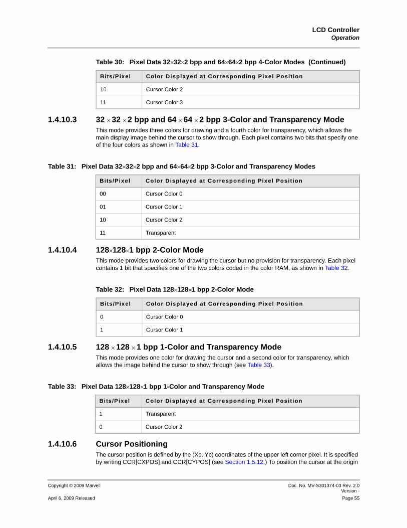
LCD ControllerOperation
Copyright © 2009 Marvell Doc. No. MV-S301374-03 Rev. 2.0Version -
April 6, 2009 Released Page 55
12345678910111213141516171819202122232425262728293031323334353637383940414243444546474849505152535455565758
1.4.10.3 32 × 32 × 2 bpp and 64 × 64 × 2 bpp 3-Color and Transparency ModeThis mode provides three colors for drawing and a fourth color for transparency, which allows the main display image behind the cursor to show through. Each pixel contains two bits that specify one of the four colors as shown in Table 31.
1.4.10.4 128×128×1 bpp 2-Color ModeThis mode provides two colors for drawing the cursor but no provision for transparency. Each pixel contains 1 bit that specifies one of the two colors coded in the color RAM, as shown in Table 32.
1.4.10.5 128 × 128 × 1 bpp 1-Color and Transparency ModeThis mode provides one color for drawing the cursor and a second color for transparency, which allows the image behind the cursor to show through (see Table 33).
1.4.10.6 Cursor PositioningThe cursor position is defined by the (Xc, Yc) coordinates of the upper left corner pixel. It is specified by writing CCR[CXPOS] and CCR[CYPOS] (see Section 1.5.12.) To position the cursor at the origin
10 Cursor Color 2
11 Cursor Color 3
Table 30: Pixel Data 32×32×2 bpp and 64×64×2 bpp 4-Color Modes (Continued)
Bits /Pixel Color Displayed at Corresponding Pixel Posit ion
Table 31: Pixel Data 32×32×2 bpp and 64×64×2 bpp 3-Color and Transparency Modes
Bits /Pixel Color Displayed at Corresponding Pixel Posit ion
00 Cursor Color 0
01 Cursor Color 1
10 Cursor Color 2
11 Transparent
Table 32: Pixel Data 128×128×1 bpp 2-Color Mode
Bits /Pixel Color Displayed at Corresponding Pixel Position
0 Cursor Color 0
1 Cursor Color 1
Table 33: Pixel Data 128×128×1 bpp 1-Color and Transparency Mode
Bits /Pixel Color Displayed at Corresponding Pixel Position
1 Transparent
0 Cursor Color 2

PXA3xx (88AP3xx) Processor FamilyVolume III: Graphics and Input Controller Configuration Developers Manual
Doc. No. MV-S301374-03 Rev. 2.0 Version -
Copyright © 2009 Marvell
Page 56 April 6, 2009 Released
12345678910111213141516171819202122232425262728293031323334353637383940414243444546474849505152535455565758
(upper left corner) of the display frame, the cursor position (Xc, Yc) value must be (0,0). The cursor is displayed partly or not displayed at all, depending on the cursor position (Xc, Yc).
It is possible to change the mode or position of the cursor while the cursor is enabled by writing the new position or mode to the Cursor Control register and then writing the start Descriptor address to the DMA Frame Branch register for Channel 5 (FBR5). The palette for the cursor must be reloaded whenever the cursor mode or position is changed. The cursor with the new size, pixel format, and position is displayed when the branch specified in the DMA Frame Branch registers (FBRx) has completed and the LCD has reached the start of the cursor position on the next frame. If the DMA Frame Branch register for Channel 5 is written when the DMA is in Descriptor-fetch mode for the cursor channel, the branch does not occur until the next frame.
Consequently, even though the palette RAM and palette buffer data remain the same, the Cursor Frame Branch register must be rewritten with the same DMA Descriptor address. Wait for the cursor branch-status interrupt to occur before updating the size, pixel format, or position of the cursor again. The same procedure is used for disabling the cursor.
The building mechanism for cursor data is similar to that for 8bpp or 4bpp frame data. The following pseudocode illustrates the process for initializing the hardware cursor:
FUNCTION Cursor_Init
CCR[CURMS] = Cursor_Mode_Select;CCR[CXPOS] = Initial_X_Position;CCR[CYPOS] = Initial_Y_Position;CCR[CEN] = 1;
CASE CCR[CURMS] of condition 0:condition 1:condition 2:
CurPatternSize = (32*32)/4; condition 3: condition 4: condition 5:
CurPatternSize = (64*64)/4; condition 6:condition 7:
CurPatternSize = (128*128)/8;END CASE
/* Palette for cursor */Build Palette for Cursor colors
/* Cursor frame data */FOR i=0 to i < CurPatternSize
CursorLocation + i = Pattern; // index of palette bufferEND FOR
END FUNCTION
The following pseudocode illustrates the process for positioning the cursor:
FUNCTION CurSor_Positioning
FBR5[SRCADDR] = CURSOR_descriptor_Addr; FBR5[BINT] = 1;FBR5[BRA] = 1;
IF LCSR1[BS5] == 1CCR[CXPOS] = NewX;CCR[CYPOS] = NewY;FBR5[BRA] = 1;
ENDIF

LCD ControllerOperation
Copyright © 2009 Marvell Doc. No. MV-S301374-03 Rev. 2.0Version -
April 6, 2009 Released Page 57
12345678910111213141516171819202122232425262728293031323334353637383940414243444546474849505152535455565758
IF NO_MORE_POSITION_CHANGEFBR5[BINT] = 0;
ENDIF
END FUNCTION
Incorrect operation of the LCD may result if the LCD controller is disabled while processing a frame (branch-status interrupt did NOT occur). Always ensure that a frame-branch interrupt occurs before disabling the LCD controller.
Figure 14: Cursor Position within Display Frame
1.4.10.7 Cursor Color MapThe color map, which defines the colors used by the cursor, has four 24-bit-wide locations and is loaded from either internal or external memory through DMA Channel 5.
1.4.11 External Palette BufferThe palette data for each overlay is stored in either internal memory or external memory, which is referred to as the palette buffer. Palette data for the base, Overlay 1, and Overlay 2 can be up to 256 x 25 bits. Palette data is 256 entries. The palette RAM is not used for pixel depths greater then 8 bpp. Load the palette RAM at least once if it is to be used; afterward, reloading the palette is optional for every frame.
1.4.11.1 Palette Data FormatsFigure 15 through Figure 18 show the pixel format for palette data stored in the palette buffer for various pixel depths. These are used only when the pixel data in the frame buffer is less then 16 bits. If transparency is not used and the bpp is less then 18 bits, the palette data must be in the appropriate format specified in Figure 15. If transparency is used, the palette data must be in the appropriate format specified in Figure 16 through Figure 18. The palette data is programmed to one of the formats by programming LCCR4[PAL_FOR]. In 16-bit and 18-bit palette format with transparency bit, the red, green, and blue components must be expanded to 8 bits (each color) by padding zeros to the right as shown in the corresponding figure.
(Xc, Yc)
Origin of Display
Display Frame
cursor
Figure 15: Palette Data Formats—Transparency Disabled
16-Bit Palette Format without Transparency Bit for Color Panel
Bit 15 14 13 12 11 10 9 8 7 6 5 4 3 2 1 0

PXA3xx (88AP3xx) Processor FamilyVolume III: Graphics and Input Controller Configuration Developers Manual
Doc. No. MV-S301374-03 Rev. 2.0 Version -
Copyright © 2009 Marvell
Page 58 April 6, 2009 Released
12345678910111213141516171819202122232425262728293031323334353637383940414243444546474849505152535455565758
1.4.11.2 Little-Endian FormatThe palette entries must be in little-endian format. Endian does not imply endianness with respect to bytes and half-words within memory. It refers strictly to the ordering of the palette entries; palette entry 0 is located at the LSB of a word boundary. The ordering of RGB values within the entry is fixed. Figure 19 shows the format in which the palette data is stored in the palette buffer.
Color Red (R) Green (G) Blue (B)
Figure 15: Palette Data Formats—Transparency Disabled
Figure 16: Palette Data Formats 0b01—Transparency Enabled
16-Bit Palette Format with Transparency Bit for Color Panel
Bit 24 23 22 21 20 19 18 17 16 15 14 13 12 11 10 9 8 7 6 5 4 3 2 1 0
Color T Red[4:0] 0 0 0 Green[5:0] 0 0 Blue[4:0] 0 0 0
Note: T bit is the transparency bit. It should be zero-value when transparency is not intended.
Figure 17: Palette Data Formats 0b10—Transparency Enabled
18-Bit Palette Format with Transparency Bit for Color Panel
Bit 24 23 22 21 20 19 18 17 16 15 14 13 12 11 10 9 8 7 6 5 4 3 2 1 0
Color T Red[5:0] 0 0 Green[5:0] 0 0 Blue[5:0] 0 0
Note: T bit is the transparency bit. It should be zero-value when transparency is not intended.
Figure 18: Palette Data Formats 0b11—Transparency Enabled
25-Bit Palette Format with Transparency Bit for Color Panel
Bit 24 23 22 21 20 19 18 17 16 15 14 13 12 11 10 9 8 7 6 5 4 3 2 1 0
Color T Expanded Red[7:0] Expanded Green[7:0] Expanded Blue[7:0]
Note: T bit is the transparency bit. It should be zero-value when transparency is not intended.
Figure 19: Format for Palette Data
Palette Entry Ordering256-Entry Palette Buffer
Bit 31 16 15 0
0x0 Palette entry 1 Palette entry 0
0x4 Palette entry 3 Palette entry 2
0x1C Palette entry 15 Palette entry 14
0x20 Palette entry 17 Palette entry 16

LCD ControllerOperation
Copyright © 2009 Marvell Doc. No. MV-S301374-03 Rev. 2.0Version -
April 6, 2009 Released Page 59
12345678910111213141516171819202122232425262728293031323334353637383940414243444546474849505152535455565758
1.4.12 Frame BufferThe frame data for the base, Overlay 1, and Overlay 2 is stored in the frame buffers that reside in either internal or external memory. Each plane used (base plane, Overlay 1, Overlay 2, cursor, and command RAM) requires its own frame buffer to store the pixel data for that plane. Additionally, if a palette is used, a palette buffer (a small memory area that maps the palette colors to the LCD colors) is required. All the planes could use the same palette buffer, or each plane could have a separate palette buffer, depending on system design preferences.
The amount of the pixel data for each layer depends on the size of the screen (for example, 640 × 480 = 307,200 encoded pixel values as described in Section 1.4.3). The diagrams in this section show the memory organization within the frame buffer for each pixel size. The pixel entries are ordered starting with the least significant bit and ending with the most significant bit in a 32-bit word.
Each line in the memory must start at a word boundary. For the various pixel sizes, this requires each line of the display to have pixels in multiples of the following:
4 pixels for 8-bit pixels
2 pixels for pixel depth of 16 bpp active8 pixels for packed 18- or 19-bit pixels16 pixels for Overlay 2 frame when the data is in 4:2:0 YCbCr format
If the number of pixels per line of the LCD screen does not meet the requirements listed above, the number of pixels per line should be adjusted by adding an extra pixel to meet the above requirements and the panel should ignore the extra pixels. This ensures that each line in the memory is word-aligned. For example, if the screen that is being driven is 177 pixels wide, and 8-bits/pixel mode is used, each line is 177 pixels, or bytes, in length. The next nearest 4-pixel boundary (for 8-bit pixels) occurs at 180 pixels or 180 bytes. Thus, each new line must start in the
0x1FC Palette entry 255 Palette entry 254
Palette Entry Ordering with Overlays Enabled256-Entry Palette Buffer
Bit 31 24 17 16 15 0
0x0 Unused Palette entry 0
0x4 Unused Palette entry 1
0x8 Unused Palette entry 2
0xC Unused Palette entry 3
0x38 Unused Palette entry 14
0x3C Unused Palette entry 15
0x3FC Unused Palette entry 255
Figure 19: Format for Palette Data (Continued)
Palette Entry Ordering256-Entry Palette Buffer

PXA3xx (88AP3xx) Processor FamilyVolume III: Graphics and Input Controller Configuration Developers Manual
Doc. No. MV-S301374-03 Rev. 2.0 Version -
Copyright © 2009 Marvell
Page 60 April 6, 2009 Released
12345678910111213141516171819202122232425262728293031323334353637383940414243444546474849505152535455565758
frame buffer at multiples of 180 bytes by adding an extra three dummy pixels per line (3 bytes). These restrictions also apply to panels with an internal frame buffer.
1.4.12.1 Memory Organization for Pixel Depth of 8 bppFigure 20 shows the format of pixel data stored in memory for a depth of 8 bits per pixel.
1.4.12.2 Memory Organization for Pixel Depth of 16 bppFigure 21 shows the format of pixel data stored in memory for a depth of 16 bits per pixel.
1.4.12.3 Memory Organization for Pixel Depth of 18 bpp Figure 22 shows the format of pixel data stored in memory for an unpacked depth of 18 bits per pixel.
Figure 20: Memory Organization for Pixel Depth of 8 bpp
Bit 7 6 5 4 3 2 1 0
8 bpp Encoded Pixel Data[7:0]
Bit 31 24 23 16 15 8 7 0
0x0 Pixel 3 Pixel 2 Pixel 1 Pixel 0
0x4 Pixel 7 Pixel 6 Pixel 5 Pixel 4
Figure 21: Memory Organization for Pixel Depth of 16 bpp
Bit 15 14 13 12 11 10 9 8 7 6 5 4 3 2 1 0
16 bppOverlay Disabled
Red[4:0] Green[5:0] Blue[4:0]
16 bppOverlays Enabled
T Red[4:0] Green[4:0] Blue[4:0]
Memory Organizat ion
Bit 31 16 15 0
0x0 Pixel 1 Pixel 0
0x4 Pixel 3 Pixel 2
Figure 22: Memory Organization for Pixel Depth of 18 bpp Unpacked
Bit 17 12 11 6 5 0
18 bpp Red[5:0] Green[5:0] Blue[5:0]
Memory Organization
Bit 31 18 17 0
0x0 Unused Pixel 0
0x4 Unused Pixel 1

LCD ControllerOperation
Copyright © 2009 Marvell Doc. No. MV-S301374-03 Rev. 2.0Version -
April 6, 2009 Released Page 61
12345678910111213141516171819202122232425262728293031323334353637383940414243444546474849505152535455565758
Figure 23 shows the format of pixel data stored in memory for a unpacked pixel depth of 18 bits per pixel in (6R+2’0s, 6G+2’0s, 6B+2’0s) for the PXA31x processor.
Figure 24 shows the format of pixel data stored in memory for a packed depth of 18 bits per pixel.
Figure 25 shows the format of pixel data stored in memory for a packed pixel depth of 18 bits per pixel in (6R+2’0s, 6G+2’0s, 6B+2’0s) for the PXA31x processor.
Figure 23: Memory Organization for Pixel Depth of 18 bpp Unpacked in (6R+2’0s, 6G+2’0s, 6B+2’0s) Format
Bit 23 22 21 20 19 18 17 16 15 14 13 12 11 10 9 8 7 6 5 4 3 2 1 0
18 bpp Red[5:0] 0 0 Green[5:0] 0 0 Blue[5:0] 0 0
Memory Organization
Bit 31 24 23 0
0x0 Unused Pixel 0
0x4 Unused Pixel 1
NOTE:PXA31x processor only
Figure 24: Memory Organization for Pixel Depth of 18 bpp Packed
Bit 17 12 11 6 5 0
18 bpp Red Data[5:0] Green Data[5:0] Blue Data[5:0]
Memory Organizat ion
Bit 31 24 23 16 15 8 7 0
0x0 pixel1[7:0] {[000000], pixel0[17:0]}
0x4 pixel2[15:0] {[000000], pixel1[17:8]}
0x8 {[000000], pixel3[17:0]} {[000000], pixel2[17:16]}
Note: The data is not packed across frame line but only in each individual frame lines.
Figure 25: Memory Organization for Pixel Depth of 18 bpp Packed in (6R+2’0s, 6G+2’0s, 6B+2’0s)
Bit 23 . . 18 17 16 15 . . 10 9 8 7 . . 2 1 0
18 bppRed[5:0] 0 0
Green[5:0]Blue[5:0
0 0
NOTE: PXA31x processor only
Memory Organization
Bit 31 24 23 16 15 8 7 0
0x0 pixel1[7:0] pixel0[23:0]
0x4 pixel2[15:0] pixel1[23:8]
0x8 pixel3[23:0] pixel2[23:16]

PXA3xx (88AP3xx) Processor FamilyVolume III: Graphics and Input Controller Configuration Developers Manual
Doc. No. MV-S301374-03 Rev. 2.0 Version -
Copyright © 2009 Marvell
Page 62 April 6, 2009 Released
12345678910111213141516171819202122232425262728293031323334353637383940414243444546474849505152535455565758
1.4.12.4 Memory Organization for Pixel Depth of 19 bppFigure 26 shows the format of pixel data stored in memory for an unpacked pixel depth of 19 bits per pixel.
Figure 27 shows the format of pixel data stored in memory for an unpacked pixel depth of 19 bits per pixel in (6R+2’0s, 6G+2’0s, 6B+2’0s) for the PXA31x processor.
Figure 28 shows the format of pixel data stored in memory for a packed depth of 19 bits per pixel.
Note: The data is not packed across frame line but only in each individual frame lines.
Figure 25: Memory Organization for Pixel Depth of 18 bpp Packed in (6R+2’0s, 6G+2’0s, 6B+2’0s)
Bit 23 . . 18 17 16 15 . . 10 9 8 7 . . 2 1 0
Figure 26: Memory Organization for Pixel Depth of 19 bpp Unpacked
Bit 18 17 12 11 6 5 0
19 bits/pixel
T Red [5:0] Green [5:0] Blue [5:0]
Memory Organization
Bit 31 24 23 0
0x0 Unused {[00000], pixel0[18:0]}
0x4 Unused {[00000], pixel1[18:0]}
Figure 27: Memory Organization for Pixel Depth of 19bpp Unpacked in (6R+2’0s, 6G+2’0s, 6B+2’0s) Format
Bit 24 23 22 21 20 19 18 17 16 15 14 13 12 11 10 9 8 7 6 5 2 1 0
18 bppT Red[5:0] 0 0 Green[5:0] 0 0 Blue[5:0] 0 0
Memory Organizat ion
Bit 31 24 23 0
0x0 Unused Pixel 0
0x4 Unused Pixel 1
NOTE: PXA31x processor only
Figure 28: Memory Organization for Pixel Depth of 19 bpp Packed
Bit 18 17 12 11 6 5 0
19 bits/pixel
T Red[5:0] Green[5:0] Blue[5:0]
Memory Organization
Bit 31 24 23 7 0
0x0 pixel1[7:0] {[00000], Pixel 0[18:0]}

LCD ControllerOperation
Copyright © 2009 Marvell Doc. No. MV-S301374-03 Rev. 2.0Version -
April 6, 2009 Released Page 63
12345678910111213141516171819202122232425262728293031323334353637383940414243444546474849505152535455565758
1.4.12.5 Memory Organization for Pixel Depth of 24 bppFigure 29 shows the format of pixel data stored in memory for a pixel depth of 24 bits per pixel.
Note
Note Configuring the LCD controller for 24-bpp output is not valid for panels without an internal frame buffer (LCCR0[LCDT] clear) and results in indeterminate behavior.
)
1.4.12.6 Memory Organization for Pixel Depth of 25 bppFigure 30 shows the format of pixel data stored in memory for a depth of 25 bits per pixel.
Note
Note Configuring the LCD controller for 25-bpp output is not valid for panels that are not smart panels (LCCR0[LCDT] clear) and does result in indeterminate behavior.
0x4 pixel 2[15:0] {[00000], pixel1[18:8]}
0x8 {[00000], pixel 3[18:0]} {[00000],pixel2[18:16]}
Note: The data is not packed across frame line but only in each individual frame lines.
Figure 28: Memory Organization for Pixel Depth of 19 bpp Packed
Figure 29: Memory Organization for Pixel Depth of 24 bpp
Bit 23 22 16 15 14 8 7 6 0
24 bpp(Overlays Disabled)
Red[7:0] Green[7:0] Blue[7:0]
24 bpp (Overlays Enabled)
T Red[7:0] Green[7:0] Blue[6:0]
24-Bit Mode(Overlays Enabled)1
Red[7:0] Green[7:0] Blue[7:0]
Memory Organization
Bit 31 24 23 0
0x0 Unused Pixel 0
0x4 Unused Pixel 1
1.This format is available only for Overlay 1. The value of PDFOR is ignored for this mode. OVL1C1[BPP1] = 0x0 for this mode.
Figure 30: Memory Organization for Pixel Depth of 25 bpp
Bit 24 23 16 15 8 7 0

PXA3xx (88AP3xx) Processor FamilyVolume III: Graphics and Input Controller Configuration Developers Manual
Doc. No. MV-S301374-03 Rev. 2.0 Version -
Copyright © 2009 Marvell
Page 64 April 6, 2009 Released
12345678910111213141516171819202122232425262728293031323334353637383940414243444546474849505152535455565758
1.4.12.7 Memory Organization for 4:4:4 YCbCr Packed FormatFigure 31 shows the format of pixel data stored in memory for a 4:4:4 YCbCr packed format.
1.4.13 Functional TimingRefer to Figure 32 through Figure 36 for LCD controller pin timing diagrams. Figure 32 shows the output pin timing. The LCD controller is enabled when LCCR0[ENB] is set to 1. Bits LCCR3[VSP], LCCR3[HSP], and LCCR3[PCP] define the polarity of the frame clock, line clock and pixel clock, respectively.
1.4.13.1 Passive Mode TimingFor passive (and active) LCD panels, the line-clock pin (L_LCLK_A0) is toggled when an entire line of pixels is output to the LCD controller screen. Similarly, the frame-clock pin (L_FCLK_RD) is toggled when an entire frame of pixels is output to the LCD controller screen.
The power and ground supplies must be switched periodically to prevent a DC charge from building within a passive display. The LCD controller signals the display to switch the polarity by toggling the AC bias pin (L_BIAS). Control the frequency of the bias pin by programming the number of line-clock transitions between each toggle.The timing of the line and frame clock pins is programmable to support both passive and active modes. Programming options include:
Wait-state insertion both at the beginning and end of each line and framePixel clock
Line clockFrame clockOutput-enable signal polarity
Frame-clock pulse width
25 bpp T Red Data[7:0] Green Data[7:0] Blue Data[7:0]
Memory Organization
Bit 31 25 24 0
0x0 Unused Pixel 0
0x4 Unused Pixel 1
Figure 30: Memory Organization for Pixel Depth of 25 bpp
Figure 31: Memory Organization for 4:4:4 YCbCr Packed Format
Bit 23 16 15 8 7 0
Cr Data [7:0] Cb Data [7:0] Y Data [7:0]
Memory Organization
Bit 31 24 23 0
0x0 Unused Pixel 0
0x4 Unused Pixel 1
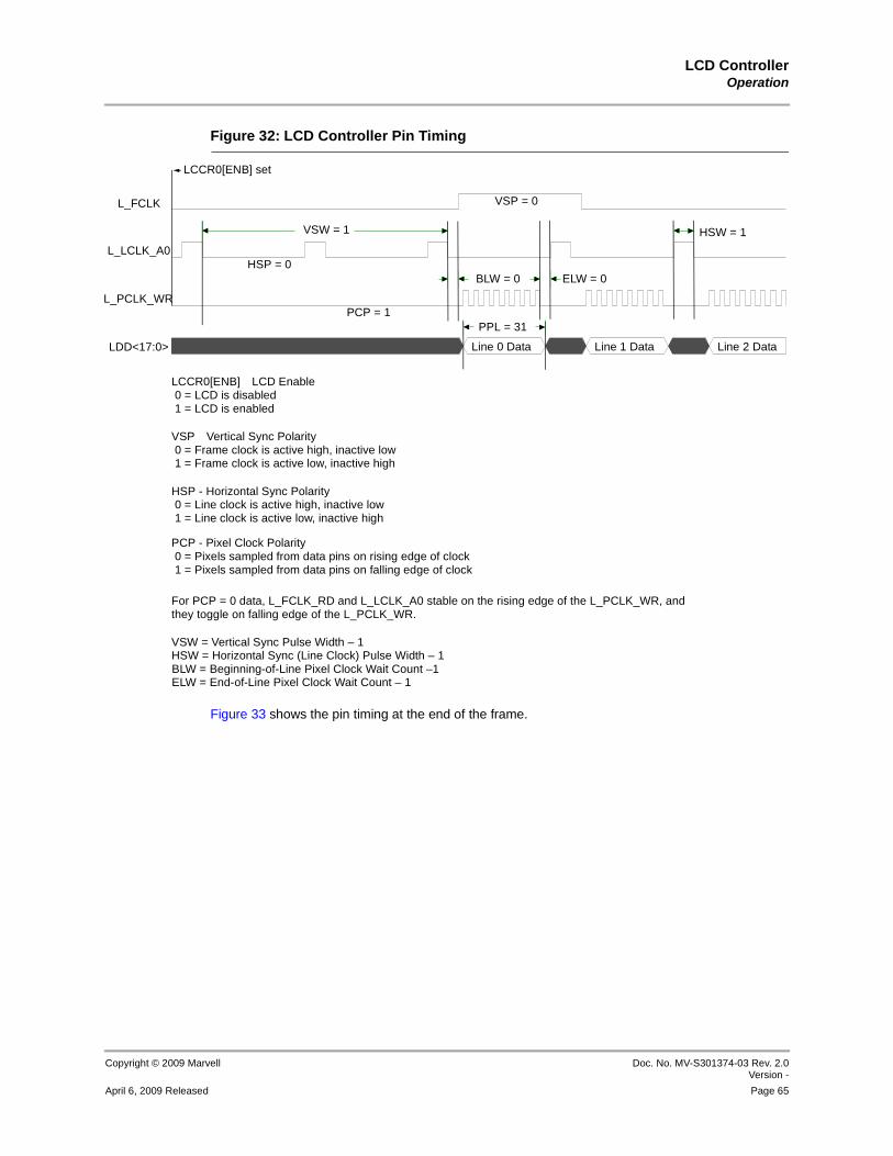
LCD ControllerOperation
Copyright © 2009 Marvell Doc. No. MV-S301374-03 Rev. 2.0Version -
April 6, 2009 Released Page 65
12345678910111213141516171819202122232425262728293031323334353637383940414243444546474849505152535455565758
Figure 32: LCD Controller Pin Timing
Figure 33 shows the pin timing at the end of the frame.
Line 0 Data Line 1 Data Line 2 Data
PPL = 31
ELW = 0 BLW = 0
HSW = 1 VSW = 1
LCCR0[ENB] LCD Enable 0 = LCD is disabled 1 = LCD is enabled
VSP Vertical Sync Polarity 0 = Frame clock is active high, inactive low 1 = Frame clock is active low, inactive high
HSP - Horizontal Sync Polarity 0 = Line clock is active high, inactive low 1 = Line clock is active low, inactive high
PCP - Pixel Clock Polarity 0 = Pixels sampled from data pins on rising edge of clock 1 = Pixels sampled from data pins on falling edge of clock
For PCP = 0 data, L_FCLK_RD and L_LCLK_A0 stable on the rising edge of the L_PCLK_WR, and
VSW = Vertical Sync Pulse Width – 1HSW = Horizontal Sync (Line Clock) Pulse Width – 1BLW = Beginning-of-Line Pixel Clock Wait Count –1ELW = End-of-Line Pixel Clock Wait Count – 1
L_FCLK
L_LCLK_A0
L_PCLK_WR
LDD<17:0>
LCCR0[ENB] set
PCP = 1
VSP = 0
HSP = 0
they toggle on falling edge of the L_PCLK_WR.

PXA3xx (88AP3xx) Processor FamilyVolume III: Graphics and Input Controller Configuration Developers Manual
Doc. No. MV-S301374-03 Rev. 2.0 Version -
Copyright © 2009 Marvell
Page 66 April 6, 2009 Released
12345678910111213141516171819202122232425262728293031323334353637383940414243444546474849505152535455565758
Figure 33: Passive Mode End-of-Frame Timing
1.4.13.2 Active Mode TimingFor active (and passive) LCD panels, the line-clock pin (L_LCLK_A0) is toggled when an entire line of pixels has been output to the LCD controller screen. Likewise, the frame-clock pin (L_FCLK_RD) is toggled when an entire frame of pixels has been output to the LCD panel.
The pixel clock toggles continuously in this mode as long as the LCD is enabled. The AC bias pin (L_BIAS) functions as an output enable. The display latches data from the LCD pins using the pixel clock when L_BIAS is asserted. The line clock pin (L_LCLK_A0) is used as the horizontal synchronization signal and the frame clock (L_FCLK_RD) as the vertical synchronization signal. The timing of the line and frame clock pins is programmable to support both passive and active mode. Programming options include: wait-state insertion both at the beginning and end of each line and frame; pixel clock; line clock; frame clock; output-enable signal polarity; and frame-clock pulse width.
Figure 34 shows output pin timing in active mode.
Line 63 Data Line 0 Data
PPL = 23
BLW = 0 ELW = 0
VSW = 2 HSW = 1
LCCR0[ENB] LCD Enable 0 = LCD is disabled 1 = LCD is enabled
VSP Vertical Sync Polarity 0 = Frame clock is active high, inactive low 1 = Frame clock is active low, inactive high
HSP Horizontal Sync Polarity 0 = Line clock is active high, inactive low 1 = Line clock is active low, inactive high
PCP Pixel Clock Polarity 0 = Pixels sampled from data pins on rising edge of clock 1 = Pixels sampled from data pins on falling edge of clock
For PCP = 0 and for PCP = 1, data is driven out at the same time; L_PCLK_WR is simply inverted for PCP = 1
VSW = Vertical Sync Pulse Width – 1HSW = Horizontal Sync (Line Clock) Pulse Width – 1BLW = Beginning-of-Line Pixel Clock Wait Count – 1ELW = End-of-Line Pixel Clock Wait Count – 1PPL = Pixels Per Line – 1
L_FCLK
L_LCLK_A0
L_PCLK_WR
LDD<7:0>
LCCR0[ENB] set
PCP = 1
VSP = 0
HSP = 0
LPP = Lines Per Panel – 1
LPP = 63

LCD ControllerOperation
Copyright © 2009 Marvell Doc. No. MV-S301374-03 Rev. 2.0Version -
April 6, 2009 Released Page 67
12345678910111213141516171819202122232425262728293031323334353637383940414243444546474849505152535455565758
Figure 34: Active Mode Timing
Line 0 Data Line 1 Data Line 2 Data
PPL = 7
ELW = 0 BLW = 0
BFW = 1 HSW = 1
VSW = 0
ENB LCD Enable 0 = LCD is disabled 1 = LCD is enabled
VSP Vertical Sync Polarity 0 = Vertical sync clock is active high, inactive low; vertical sync pulse is high (VSW+1) HSYNC clocks.
1 = Vertical sync clock is active low, inactive high; vertical sync pulse is low (VSW+1) HSYNC clocks.
HSP Horizontal Sync Polarity 0 = Horizontal sync clock is active high, inactive low; horizontal sync pulse is high (HSW+1) pixel clocks.
1 = Horizontal sync clock is active low, inactive high; horizontal sync pulse is low (HSW+1) pixel clocks.
PCP - Pixel Clock Polarity 0 = Pixels sampled from data pins on the rising edge of clock; HSYNC and VSYNC signals change levels
1 = Pixels sampled from data pins on the falling edge of clock; HSYNC and VSYNC change levels
For PCP = 0 and for PCP = 1, data is driven out at the same time; L_PCLK_WR is simply inverted for PCP = 1.
VSW = Vertical Sync Pulse Width – 1HSW = Horizontal Sync Pulse Width – 1BFW = Beginning-of-Frame Horizontal Sync Clock Wait CountBLW = Beginning-of-Line Pixel Clock Wait Count – 1ELW = End-of-Line Pixel Clock Wait Count – 1PPL = Pixels Per Line – 1
L_FCLK_RD(VSYNC)
L_LCLK_A0(HSYNC)
L_BIAS(OE)
L_PCLK_WR
LDD<17:0>
VSP = 0
HSP = 0
PCP = 0
PCP - Pixel Clock Polarity
Data is fetched when VSYNC is low.
Data is fetched when VSYNC is high.
Data is fetched when HSYNC is low.
Data is fetched when HSYNC is high.
on the rising edge of the pixel clock.
on the falling edge of the pixel clock.

PXA3xx (88AP3xx) Processor FamilyVolume III: Graphics and Input Controller Configuration Developers Manual
Doc. No. MV-S301374-03 Rev. 2.0 Version -
Copyright © 2009 Marvell
Page 68 April 6, 2009 Released
12345678910111213141516171819202122232425262728293031323334353637383940414243444546474849505152535455565758
Figure 35 shows the output data pin timing in active mode.
Figure 35: Active Mode Pixel Clock and Data Pin Timing
1.4.13.3 Smart Panel Mode TimingFor smart panels (LCD panels with internal frame-buffer memory), the data is written into the frame buffer memory within the smart panel. This allows the smart panel to refresh the LCD panel without the PXA30x and PXA31x processors constantly writing the pixel data over the LCD pins. The LCD controller only needs to toggle the LCD pins when the pixel data changes or when a new command needs to be sent to the smart panel.
The timing is similar to that of microcontroller commands. Each command contains 8 bits of data (transferred on LDD<7:0>) and is identified as either an address or data command by L_LCLK_A0. L_PCLK_WR and L_FCLK_RD are used to specify whether a Read or Write command is issued. L_CS is the chip select signal for the panel. At the beginning of each frame, the LCD controller sends one or more command sequences from the command RAM, followed by the frame data. The interface timing is shown in Figure 36.
Pixel 0 Pixel 1 Pixel 2 Pixel 3 Pixel 4
PCP Pixel Clock Polarity 0 = Pixels sampled from data pins on rising edge of clock 1 = Pixels sampled from data pins on falling edge of clock
For PCP = 1 data is driven out at the same time and L_PCLK is inverted.
L_FCLK_RD(VSYNC)
L_LCLK_A0(HSYNC)
L_BIAS(OE)
L_PCLK_WR
LDD<17:0>
PCP = 0

LCD ControllerOperation
Copyright © 2009 Marvell Doc. No. MV-S301374-03 Rev. 2.0Version -
April 6, 2009 Released Page 69
12345678910111213141516171819202122232425262728293031323334353637383940414243444546474849505152535455565758
Figure 36: Interface with SMART Panels Timing
1.4.14 Using the LCD Controller Data PinsPixel data is removed from the bottom of the output FIFO and is driven in parallel onto the LCD data lines on the edge selected by the pixel-clock polarity bit (LCCR3[PCP]). For an 8-bit wide bus interface, the data is driven onto LDD<7:0>. For a 16-bit-wide bus interface, the data is driven onto LDD<15:0>. For 18-bit-wide bus interface, the data is driven onto LDD<17:0>.
The assignment of the LCD output is assigned to the actual LDD pins using alternate multiplexing functions. Table 34 shows the LCD data pins for each operating mode and the order of pixels delivered to a screen for each. Figure 37 shows the LCD data-pin pixel ordering for passive panels.
DWR_HLD
DWR_SET
A0CSWR_HLDA0CSWR_SET
Data Data
Write
A0CSWR_SET = A0 and CS Setup Time before L_PCLK_WR is asserted = LCCR1[ELW] + 1
A0CSWR_HLD = A0 and CS Hold Time after L_PCLKWR is de-asserted = LCCR1[ELW] + 1
DWR_SET = Data Setup Time before L_PCLK_WR is asserted = LCCR1[ELW] + 1
DWR_HLD = Data Hold Time after L_PCLK_WR is de-asserted = LCCR1[ELW] + 1
L_FCLK_RD and L_PCLK_WR are programmed by the same register bit settings and all the setup, hold, and pulse
L_CS
L_LCLK_A0
L_PCLK_WR
LDD<7:0>
CMD_INH
CMD_INH = Command Inhibit time between two writes = LCCR3[PCD] + 1
L_FCLK_RD
A0CSRD_SET
A0CSRD_HLDWR_PULWD
RD_PULWD
A0CSRD_SET = A0 and CS Setup Time before L_FCLK_RD is asserted = LCCR1[ELW] + 1
A0CSRD_HLD = A0 and CS Hold Time after L_FCLK_RD is de-asserted = LCCR1[ELW] + 1
WR_PULWD = L_PCLK_WR pulse width = LCCR1[BLW] + 1
RD_PULWD = L_FCLK_RD pulse width = LCCR1[BLW] + 1
OP_HLD
RD_ACC = Read Access Time is specific to the LCD panel. Refer to the manufacturer’s specification sheet for this time.
RD_ACC
OP_HLD = Output Hold time from L_FCLK_RD negation = LCCR1[HSW]
widths are the same for these 2 signals
Read
Note: All times are programmed in units of the LCLK period that is 60 MHz in D0CS and either 104 or 208 MHz in D0.
CS_INH
.
CS_INH = Time between de-assertion of CS and Assertion of CS for the next transaction. The minimum time for thisis 2 LCLK periods during frame write command.

PXA3xx (88AP3xx) Processor FamilyVolume III: Graphics and Input Controller Configuration Developers Manual
Doc. No. MV-S301374-03 Rev. 2.0 Version -
Copyright © 2009 Marvell
Page 70 April 6, 2009 Released
12345678910111213141516171819202122232425262728293031323334353637383940414243444546474849505152535455565758
.
Figure 37: LCD Data-Pin Pixel Ordering
For color mode, for all pixel depths (8, 16, 18, 19, 24 and 25 bpp) the pixel value from the combination logic goes through the dither logic that produces one bit for each color (red, green, and blue), which get loaded into the 8-bit wide output FIFO. When the FIFO is loaded with 8 bits, they are driven in parallel onto the data bus LDD<7:0>, as shown in Table 35.
1.4.14.1 16-Bit Interface for Active For a pixel depth of 16 bpp, the data is driven in parallel onto the 16-bit data bus LDD<15:0>, as shown in Table 36.
Table 34: LCD Controller Data Pin Usage
Panel Type Passive/Active Panel
Pins
Color Passive LDD<7:0>
Color Active LDD<15:0> or LDD<17:0> or LDD<23:0> for PXA31x
LCD Panels with Integrated Frame Buffer Both LDD<7:0>
LDD7 LDD6 LDD5 LDD4 LDD3 LDD2 LDD1 LDD0 LDD7
Top Left Corner of ScreenColumn 0 Column 0 Column 0 Column 1 Column 1 Column 1 Column 2 Column 2 Column 2
Row 0
Row 1
Row 2
Row 3
LDD7 LDD6 LDD5 LDD4 LDD3 LDD2 LDD1 LDD0 LDD7
LDD7 LDD6 LDD5 LDD4 LDD3 LDD2 LDD1 LDD0 LDD7
LDD7 LDD6 LDD5 LDD4 LDD3 LDD2 LDD1 LDD0 LDD7
Passive Color Display Pixel Ordering
Red Green Blue Red Green Blue Red Green Blue
Table 35: Color, Passive, 8-Bit Bus
LDD7 LDD6 LDD5 LDD4 LDD3 LDD2 LDD1 LDD0
R0 G0 B0 R1 G1 B1 R2 G2
B2 R3 G3 B3 R4 G4 B4 R5
G5 B5 R6 G6 B6 R7 G7 B7
Table 36: Color, Active, 16 bpp, 16-Bit Bus
LD
D1
5
LD
D1
4
LD
D1
3
LD
D1
2
LD
D1
1
LD
D1
0
LD
D9
LD
D8
LD
D7
LD
D6
LD
D5
LD
D4
LD
D3
LD
D2
LD
D1
LD
D0
Encoded Pixel0 data[15:0]

LCD ControllerOperation
Copyright © 2009 Marvell Doc. No. MV-S301374-03 Rev. 2.0Version -
April 6, 2009 Released Page 71
12345678910111213141516171819202122232425262728293031323334353637383940414243444546474849505152535455565758
1.4.14.2 18-bit Interface for ActiveFor pixel depths of 18 bpp and 19 bpp, the data is driven on to 18-bit-wide bus as shown in Table 37. .
1.4.14.3 24-bit Interface for Active for PXA31xFor pixel depths of 24bpp and 25bpp, the data is driven on to 24-bit-wide bus as shown in Table 38. .
1.4.14.4 Summary of Pin Assignments in Active ModeTable 39 lists the pin assignments for various bus widths in the possible formats.
Encoded Pixel1 data[15:0]
Table 36: Color, Active, 16 bpp, 16-Bit Bus (Continued)
LD
D1
5
LD
D1
4
LD
D1
3
LD
D1
2
LD
D1
1
LD
D1
0
LD
D9
LD
D8
LD
D7
LD
D6
LD
D5
LD
D4
LD
D3
LD
D2
LD
D1
LD
D0
Table 37: Color, Active, 18 bpp or 19 bpp, 18-Bit Bus
LD
D1
7
LD
D1
6
LD
D1
5
LD
D1
4
LD
D1
3
LD
D1
2
LD
D1
1
LD
D1
0
LD
D9
LD
D8
LD
D7
LD
D6
LD
D5
LD
D4
LD
D3
LD
D2
LD
D1
LD
D0
Encoded Pixel0 data[17:0]
Encoded Pixel1 data[17:0]
Table 38: Color, Active, 24 bpp or 25 bpp, 24-Bit Bus
LD
D2
3
LD
D2
2
....
....
LD
D3
LD
D2
LD
D1
LD
D0
Encoded Pixel0 data[23:0]
Encoded Pixel1 data[23:0]
Table 39: Pin Assignments in Active Mode
Ba
se
Fo
rma
t
Ov
erl
ay
s
PA
L_
FO
R
PD
_F
OR
LD
D2
3
LD
D2
2
LD
D2
1
LD
D2
0
LD
D1
9
LD
11
8
LD
D1
7
LD
D1
6
LD
D1
5
LD
D1
4
LD
D1
3
LD
11
2
LD
D1
1
LD
D1
0
LD
D9
LD
D8
LD
D7
LD
D6
LD
D5
LD
D4
LD
D3
LD
D2
LD
D1
LD
D0
8 bpp Disabled 0 0 NA RED<4:0> GREEN<5:0> BLUE<4:0>
8 bpp Enabled 1 3LDDALT=0
NA 0 RED<4:0> GREEN<4:0>
BLUE<4:0>

PXA3xx (88AP3xx) Processor FamilyVolume III: Graphics and Input Controller Configuration Developers Manual
Doc. No. MV-S301374-03 Rev. 2.0 Version -
Copyright © 2009 Marvell
Page 72 April 6, 2009 Released
12345678910111213141516171819202122232425262728293031323334353637383940414243444546474849505152535455565758
1.4.14.5 8-Bit Interface for Smart PanelsThe data from the output FIFO is driven onto the 8-bit-wide bus in three cycles as shown in Table 40. Data for each color (red, green, and blue) can be 5, 6, 7, and 8 depending on the pixel depths and format as discussed in Section 1.4.5. For formats with less than 8 bits for each color, the lower bits are sign extended. The sign is 1 if all the bits of each color are 1; otherwise, it is 0.
1.5 LCD Controller Register DescriptionsThe LCD controller contains 16 control registers, 35 DMA registers, two status registers, and three 256-entry palette RAMs.
8 bpp Enabled 1 3LDDALT=1
NA RED<4:0> GREEN<4:0>,GREEN<0>
BLUE<4:0>
8 bpp Disabled 2 3 NA RED<5:0> GREEN<5:0> BLUE<5:0>
8 bpp Enabled 2 0† NA RED<5:0> GREEN<5:0> BLUE<5:0>
16 bpp Disabled 0† 0 NA NA RED<4:0> GREEN<5:0> BLUE<4:0>
16 bpp Enabled 0† 3LDDALT=0
NA NA 0 RED<4:0> GREEN<4:0>
BLUE<4:0>
16 bpp Enabled 0† 3LDDALT=1
NA NA RED<4:0> GREEN<4:0>,GREEN<0>
BLUE<4:0>
18 bpp Disabled 0† 3 NA RED<5:0> GREEN<5:0> BLUE<5:0>
19 bpp Enabled 0† NA NA RED<5:0> GREEN<5:0> BLUE<5:0>
24 bpp for PXA31x
Enabled NA RED<7:0> GREEN<7:0> BLUE<7:0>
Note:† The value of this field is ignored in this mode. The use of the reset value of 0 is recommended. However, any value is
acceptable.
Table 39: Pin Assignments in Active Mode (Continued)
Ba
se
Fo
rma
t
Ov
erl
ay
s
PA
L_
FO
R
PD
_F
OR
LD
D2
3
LD
D2
2
LD
D2
1
LD
D2
0
LD
D1
9
LD
11
8
LD
D1
7
LD
D1
6
LD
D1
5
LD
D1
4
LD
D1
3
LD
11
2
LD
D1
1
LD
D1
0
LD
D9
LD
D8
LD
D7
LD
D6
LD
D5
LD
D4
LD
D3
LD
D2
LD
D1
LD
D0
Table 40: 8-Bit Interface for Smart Panels
LDD<7> LDD<6> LDD<5> LDD<4> LDD<3> LDD<2> LDD<1> LDD<0>
Pixel0 Red Data
Pixel0 Green Data
Pixel0 Blue Data

LCD ControllerLCD Controller Register Descriptions
Copyright © 2009 Marvell Doc. No. MV-S301374-03 Rev. 2.0Version -
April 6, 2009 Released Page 73
12345678910111213141516171819202122232425262728293031323334353637383940414243444546474849505152535455565758
1.5.0.1 Register SummaryTable 41 shows the registers associated with the LCD controller and the physical addresses used to access them. For easy reference, the summary table includes the page number of the detailed description for each register. The remainder of this section describes the individual registers in detail.
Table 41: LCD Controller Register Summary
Address Descript ion Page
0x4400_0000 LCD Controller Control Register 0 (LCCR0) 77
0x4400_0004 LCD Controller Control Register 1 (LCCR1) 86
0x4400_0008 LCD Controller Control Register 2 (LCCR2) 88
0x4400_000C LCD Controller Control Register 3 (LCCR3) 91
0x4400_0010 LCD Controller Control Register 4 (LCCR4) 98
0x4400_0014 LCD Controller Control Register 5 (LCCR5) 106
0x4400_0018 LCD Controller Control Register 6 (LCCR6) 112
0x4400_001C Reserved
0x4400_0020 DMA Channel 0 Frame Branch Register (FBR0) 123
0x4400_0024 DMA Channel 1 Frame Branch Register (FBR1) 123
0x4400_0028 DMA Channel 2 Frame Branch Register (FBR2) 123
0x4400_002C DMA Channel 3 Frame Branch Register (FBR3) 123
0x4400_0030 DMA Channel 4 Frame Branch Register (FBR4) 123
0x4400_0034 LCD Controller Status Register 1 (LCSR1) 132
0x4400_0038 LCD Controller Status Register 0 (LCSR0) 125
0x4400_003C LCD Controller Interrupt ID Register (LIIDR) 139
0x4400_0040 TMED RGB Seed Register (TRGBR) 119
0x4400_0044 TMED Control Register (TCR) 120
0x4400_0048– 0x4400_004F
Reserved
0x4400_0050 Overlay 1 Control Register 1 (OVL1C1) 113
0x4400_0054– 0x4400_005F
Reserved
0x4400_0060 Overlay 1 Control Register 2 (OVL1C2) 114
0x4400_0064– 0x4400_006F
Reserved
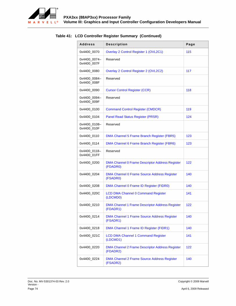
PXA3xx (88AP3xx) Processor FamilyVolume III: Graphics and Input Controller Configuration Developers Manual
Doc. No. MV-S301374-03 Rev. 2.0 Version -
Copyright © 2009 Marvell
Page 74 April 6, 2009 Released
12345678910111213141516171819202122232425262728293031323334353637383940414243444546474849505152535455565758
0x4400_0070 Overlay 2 Control Register 1 (OVL2C1) 115
0x4400_0074– 0x4400_007F
Reserved
0x4400_0080 Overlay 2 Control Register 2 (OVL2C2) 117
0x4400_0084– 0x4400_008F
Reserved
0x4400_0090 Cursor Control Register (CCR) 118
0x4400_0094– 0x4400_009F
Reserved
0x4400_0100 Command Control Register (CMDCR) 119
0x4400_0104 Panel Read Status Register (PRSR) 124
0x4400_0108– 0x4400_010F
Reserved
0x4400_0110 DMA Channel 5 Frame Branch Register (FBR5) 123
0x4400_0114 DMA Channel 6 Frame Branch Register (FBR6) 123
0x4400_0118– 0x4400_01FF
Reserved
0x4400_0200 DMA Channel 0 Frame Descriptor Address Register (FDADR0)
122
0x4400_0204 DMA Channel 0 Frame Source Address Register (FSADR0)
140
0x4400_0208 DMA Channel 0 Frame ID Register (FIDR0) 140
0x4400_020C LCD DMA Channel 0 Command Register (LDCMD0)
141
0x4400_0210 DMA Channel 1 Frame Descriptor Address Register (FDADR1)
122
0x4400_0214 DMA Channel 1 Frame Source Address Register (FSADR1)
140
0x4400_0218 DMA Channel 1 Frame ID Register (FIDR1) 140
0x4400_021C LCD DMA Channel 1 Command Register (LDCMD1)
141
0x4400_0220 DMA Channel 2 Frame Descriptor Address Register (FDADR2)
122
0x4400_0224 DMA Channel 2 Frame Source Address Register (FSADR2)
140
Table 41: LCD Controller Register Summary (Continued)
Address Descript ion Page

LCD ControllerLCD Controller Register Descriptions
Copyright © 2009 Marvell Doc. No. MV-S301374-03 Rev. 2.0Version -
April 6, 2009 Released Page 75
12345678910111213141516171819202122232425262728293031323334353637383940414243444546474849505152535455565758
The LCD controller has seven fully independent DMA channels to transfer palette data, the frame data, the cursor data, and the command data from the internal or the external memory to the LCD controller:
DMA Channel 0 is used for the base layer.
0x4400_0228 DMA Channel 2 Frame ID Register (FIDR2) 140
0x4400_022C LCD DMA Channel 2 Command Register (LDCMD2)
141
0x4400_0230 DMA Channel 3 Frame Descriptor Address Register (FDADR3)
122
0x4400_0234 DMA Channel 3 Frame Source Address Register (FSADR3)
140
0x4400_0238 DMA Channel 3 Frame ID Register (FIDR3) 140
0x4400_023C LCD DMA Channel 3 Command Register (LDCMD3)
141
0x4400_0240 DMA Channel 4 Frame Descriptor Address Register (FDADR4)
122
0x4400_0244 DMA Channel 4 Frame Source Address Register (FSADR4)
140
0x4400_0248 DMA Channel 4 Frame ID Register (FIDR4) 140
0x4400_024C LCD DMA Channel 4 Command Register (LDCMD4)
141
0x4400_0250 DMA Channel 5 Frame Descriptor Address Register (FDADR5)
122
0x4400_0254 DMA Channel 5 Frame Source Address Register (FSADR5)
140
0x4400_0258 DMA Channel 5 Frame ID Register (FIDR5) 140
0x4400_025C LCD DMA Channel 5 Command Register (LDCMD5)
141
0x4400_0260 DMA Channel 6 Frame Descriptor Address Register (FDADR6)
122
0x4400_0264 DMA Channel 6 Frame Source Address Register (FSADR6)
140
0x4400_0268 DMA Channel 6 Frame ID Register (FIDR6) 140
0x4400_026C LCD DMA Channel 6 Command Register (LDCMD6)
141
0x4400_0270– 0x440F_FFFF
Reserved
Table 41: LCD Controller Register Summary (Continued)
Address Descript ion Page

PXA3xx (88AP3xx) Processor FamilyVolume III: Graphics and Input Controller Configuration Developers Manual
Doc. No. MV-S301374-03 Rev. 2.0 Version -
Copyright © 2009 Marvell
Page 76 April 6, 2009 Released
12345678910111213141516171819202122232425262728293031323334353637383940414243444546474849505152535455565758
DMA Channel 1 is used for Overlay 1.DMA Channels 2, 3, and 4 are used for Overlay 2
Channel 5 is used for the hardware cursor. DMA Channel 6 is used to transfer data to the Command register.
The palette RAMs are always loaded through their respective DMA channels. All information for the DMA transfers is maintained in registers within the LCD DMA controller. These registers are loaded from frame Descriptors located in memory. Typically, one Descriptor is used for each frame in memory. Dedicated Descriptors are used to load the palette RAMs. Multiple Descriptors can be chained together in a list so that the DMA controller can transfer data from an essentially infinite number of discontinuous locations.
Although the FDADRx register is loaded by software, the FSADRx, FIDRx, and LDCMDx registers can only be loaded indirectly from DMA frame Descriptors. A frame Descriptor is a four-word (32-bits/word) block, aligned on a 16-byte boundary, in memory:
Word[0] contains the value for the FDADRx register.Word[1] contains the value for the FSADRx register.Word[2] contains the value for the FIDRx register.
Word[3] contains the value for the LDCMDx register.
Software should write the FDADRx register with the location of the first Descriptor before enabling the LCD controller. After the LCD controller is enabled, the first Descriptor is read, and the DMA controller writes to all four registers. The next frame Descriptor to which the FDADRx register points is loaded into the registers of the associated DMA channel after all data for the current Descriptor is transferred. The FDADRx register is bypassed only when the frame-branch register (FBRx) branch (BRA) bit is set. In this case, the frame branch address is used to fetch the Descriptor for the next frame. Branches can be used to load a new palette or just to process a regular frame. If only one frame buffer is used in external memory, program the FDADRx register to point back to itself. The DMA registers bitmaps start with Table 57. Refer to the Section 1.5.16 on DMA registers for a complete description of how the DMA is programmed.
1.5.1 LCD Controller Control Register 0 (LCCR0)LCCR0 is shown in Table 42. All bits in the control registers must be programmed before LCCR0[ENB] is set, which enables the LCD controller. A word Write can be used to configure LCCR0 while setting ENB after all other control registers are programmed. Also, the LCD controller must be disabled (by clearing LCCR0[ENB]) when changing the state of any control bit within the LCD controller. Reserved bits are unknown at reset, must be written with zeros, and may return zeros or ones when read. This is a read/write register. Ignore reads from reserved bits. Write 0b0 to reserved bits.

LCD ControllerLCD Controller Register Descriptions
Copyright © 2009 Marvell Doc. No. MV-S301374-03 Rev. 2.0Version -
April 6, 2009 Released Page 77
12345678910111213141516171819202122232425262728293031323334353637383940414243444546474849505152535455565758
Table 42: LCCR0 Bit Definitions
Physical Address0x4400_0000
LCCR0 LCD Controller
User Settings
Bit 31 30 29 28 27 26 25 24 23 22 21 20 19 18 17 16 15 14 13 12 11 10 9 8 7 6 5 4 3 2 1 0
Reserved
DE
LA
Y_
LB
IAS
LD
DA
LT
CM
DIM
RD
ST
M
LC
DT
OU
M
BS
M0
PDD
QD
M
DIS
Re
se
rve
d
Re
se
rve
d
PA
S
EO
FM
0
IUM
SO
FM
0
LD
M
Re
se
rve
d
Re
se
rve
d
EN
B
Reset ? ? ? ? 0 0 0 0 0 0 0 0 0 0 0 0 0 0 0 0 0 0 ? ? 0 0 0 0 0 ? ? 0
Bits Access Name Description
31:28 — — Reserved
27 R/W DELAY_LBIAS L_BIAS Delay Selects whether L_BIAS is delayed one additional clock cycle in active mode (PAS set).0 = L_BIAS is not delayed.1 = L_BIAS is delayed by one LCD clock in active mode. This
should be set. LCCR3[PCD] must be greater than zero when LCCR4[PCDDIV] is cleared and must be greater than 2 when LCCR4[PCDDIV] is set
26 R/W LDDALT LDD Alternate Mapping Control Bit Defines the output format of the output pixel driven on the LDD pins when Base pixel format is RGBT16 (that is, when Base bpp = 4 and PDFOR = 3 or bpp = 0 or 1 or 2 or 3, PAL_FOR = 1 AND PDFOR=3).0 = Output is driven as LDD<15:0> = '0' and (5R) and (5G) and (5B)1 = Output is driven as LDD<15:0> = (5R) and (6G) and (5B)

PXA3xx (88AP3xx) Processor FamilyVolume III: Graphics and Input Controller Configuration Developers Manual
Doc. No. MV-S301374-03 Rev. 2.0 Version -
Copyright © 2009 Marvell
Page 78 April 6, 2009 Released
12345678910111213141516171819202122232425262728293031323334353637383940414243444546474849505152535455565758
25 R/W OUC Sets Overlay 1 and Overlay 2 to function as overlays or underlays with respect to the base frame. When OUC is cleared, Overlay 1 and Overlay 2 reside below the base frame. When OUC is set, Overlay 1 and Overlay 2 reside above the Base frame.0 = Overlay 1 and Overlay 2 are underlays with respect to the base.1 = Overlay 1 and Overlay 2 are overlays with respect to the base.
Underlay Mode. Overlay 1 and Overlay 2 are underlays with respect to the base. In this mode, the order of the overlay from bottom to top is as follows:1. Overlay22. Overlay1 3. Base 4. CursorOverlay mode. Overlay 1 and Overlay 2 are overlays with respect to the Base. In this mode the order of the overlay from bottom to top is as follows:1. Base2. Overlay23. Overlay1 4. Cursor
24 R/W CMDIM LCD Command Interrupt MaskMasks interrupt requests that are asserted when the LCD controller executes an interrupt command. When CMDIM is cleared, the interrupt is enabled, and when the LCD controller executes an interrupt command in the command queue the LCSR0[CMD_INT] status bit is set, an interrupt request is made to the interrupt controller. When CMDIM is set, the interrupt is masked and the interrupt controller ignores the state of the CMD_INT status bit. Setting CMDIM does not affect the current state of CMD_INT or the LCD controller’s ability to set and clear CMD_INT; it only blocks the generation of the interrupt request.0 = Instruction “command interrupt” generates an interrupt status
sent to the interrupt controller1 = Instruction “command interrupt” does not generate an interrupt
(RD_ST status bit is ignored)
Table 42: LCCR0 Bit Definitions (Continued)
Physical Address0x4400_0000
LCCR0 LCD Controller
User Settings
Bit 31 30 29 28 27 26 25 24 23 22 21 20 19 18 17 16 15 14 13 12 11 10 9 8 7 6 5 4 3 2 1 0
ReservedD
EL
AY
_L
BIA
S
LD
DA
LT
CM
DIM
RD
ST
M
LC
DT
OU
M
BS
M0
PDD
QD
M
DIS
Re
se
rve
d
Re
se
rve
d
PA
S
EO
FM
0
IUM
SO
FM
0
LD
M
Re
se
rve
d
Re
se
rve
d
EN
B
Reset ? ? ? ? 0 0 0 0 0 0 0 0 0 0 0 0 0 0 0 0 0 0 ? ? 0 0 0 0 0 ? ? 0
Bits Access Name Description

LCD ControllerLCD Controller Register Descriptions
Copyright © 2009 Marvell Doc. No. MV-S301374-03 Rev. 2.0Version -
April 6, 2009 Released Page 79
12345678910111213141516171819202122232425262728293031323334353637383940414243444546474849505152535455565758
23 R/W RDSTM LCD Read Status Interrupt MaskMasks or enables interrupt requests that are asserted when the LCD controller executes a Read command. When RDSTM is cleared, the interrupt is enabled, and when the LCD controller reads from the panel LCSR0[RD_ST] is set, an interrupt request is made to the interrupt controller. When RDSTM is set, the interrupt is masked and the interrupt controller ignores the state of the RD_ST status bit. Setting RDSTM does not affect the current state of RD_ST or the LCD controller’s ability to set and clear RD_ST; it only blocks the generation of the interrupt request.0 = Read from the panel with frame buffer generates an interrupt
status sent to the interrupt controller1 = Read from the panel with frame buffer does not generate an
interrupt (RD_ST status bit is ignored)
22 R/W LCDT LCD Panel TypeSpecifies the type of LCD panel. When this bit is set, the LCD panel has an internal frame buffer. This changes the functionality of the interface pins. When this bit is cleared, the LCD panel is a regular panel without an internal frame buffer. 0 = LCD panel with no internal frame buffer.1 = LCD panel with internal frame buffer.
21 R/W OUM Output FIFO Underrun Mask0 = FIFO underrun errors generate an interrupt (state of OU status
sent to the interrupt controller).1 = FIFO underrun errors do not generate an interrupt (OU status
bits ignored).
Table 42: LCCR0 Bit Definitions (Continued)
Physical Address0x4400_0000
LCCR0 LCD Controller
User Settings
Bit 31 30 29 28 27 26 25 24 23 22 21 20 19 18 17 16 15 14 13 12 11 10 9 8 7 6 5 4 3 2 1 0
ReservedD
EL
AY
_L
BIA
S
LD
DA
LT
CM
DIM
RD
ST
M
LC
DT
OU
M
BS
M0
PDD
QD
M
DIS
Re
se
rve
d
Re
se
rve
d
PA
S
EO
FM
0
IUM
SO
FM
0
LD
M
Re
se
rve
d
Re
se
rve
d
EN
B
Reset ? ? ? ? 0 0 0 0 0 0 0 0 0 0 0 0 0 0 0 0 0 0 ? ? 0 0 0 0 0 ? ? 0
Bits Access Name Description

PXA3xx (88AP3xx) Processor FamilyVolume III: Graphics and Input Controller Configuration Developers Manual
Doc. No. MV-S301374-03 Rev. 2.0 Version -
Copyright © 2009 Marvell
Page 80 April 6, 2009 Released
12345678910111213141516171819202122232425262728293031323334353637383940414243444546474849505152535455565758
20 R/W BSM0 Branch Status MaskMasks or enables the interrupt requests that are asserted after branching to a new frame. When BSM0 = 0, branch status interrupts are enabled and the branch status bit (LCSR0[BS0]) is set (one), an interrupt request is made to the interrupt controller. When BSM0 = 1, branch status interrupt is masked; the state of the branch status bit is ignored by the interrupt controller. Setting BSM0 does not affect the current state of BS0 or the LCD controller ability to set and clear BS0; it only blocks the generation of the interrupt request.0 = Generates an interrupt after branching to a new frame (state of
LCSR0[BS0] sent to the interrupt controller).1 = BS condition does not generate an interrupt (LCSR0[BS0]
ignored).
19:12 R/W PDD Palette DMA Request DelaySelects the minimum number of internal bus clock cycles to wait between the servicing each DMA request issued while the internal palette RAMs are loaded. Using PDD allows other system bus masters to gain access to shared memory in between palette DMA loads. Use PDD carefully because it can severely degrade LCD controller performance if it is not used properly. Marvell recommends leaving PDD zero and adding delay only when it is necessary. PDD does not apply to normal input FIFO DMA requests for frame buffer information since these DMA requests do not occur back-to-back. The input FIFO DMA request rate is a function of the rate at which pixels are displayed on the LCD panel.Value (from 0 to 255) used to specify the number of PXCLK internal bus clocks to wait before requesting another burst of palette data. The counter starts decrementing when the first word is written to the input FIFO buffer. Programming PDD=0x0000_0000 disables this function.
Table 42: LCCR0 Bit Definitions (Continued)
Physical Address0x4400_0000
LCCR0 LCD Controller
User Settings
Bit 31 30 29 28 27 26 25 24 23 22 21 20 19 18 17 16 15 14 13 12 11 10 9 8 7 6 5 4 3 2 1 0
ReservedD
EL
AY
_L
BIA
S
LD
DA
LT
CM
DIM
RD
ST
M
LC
DT
OU
M
BS
M0
PDD
QD
M
DIS
Re
se
rve
d
Re
se
rve
d
PA
S
EO
FM
0
IUM
SO
FM
0
LD
M
Re
se
rve
d
Re
se
rve
d
EN
B
Reset ? ? ? ? 0 0 0 0 0 0 0 0 0 0 0 0 0 0 0 0 0 0 ? ? 0 0 0 0 0 ? ? 0
Bits Access Name Description

LCD ControllerLCD Controller Register Descriptions
Copyright © 2009 Marvell Doc. No. MV-S301374-03 Rev. 2.0Version -
April 6, 2009 Released Page 81
12345678910111213141516171819202122232425262728293031323334353637383940414243444546474849505152535455565758
11 R/W QDM LCD Quick Disable MaskMasks or enables interrupt requests that are asserted after the LCD enable (ENB) bit is cleared and the DMA controller finishes the current burst transfer. The LCD controller immediately stops requesting new data and the current frame is not completed. This shutdown is to be used for sleep shutdown. When QDM is cleared, the interrupt is enabled, and whenever the LCD quick disable (QD) status bit within the LCD Status register 0 (LCSR0) is set (one), an interrupt request is made to the interrupt controller. When QDM is set, the interrupt is masked and the state of the QD status bit is ignored by the interrupt controller. Setting QDM does not affect the current state of QD or the LCD controller ability to set and clear QD; it only blocks the generation of the interrupt request.0 = Generates an interrupt after quick disable (state of QD status
sent to the interrupt controller).1 = QD status does not generate an interrupt (QD status bit
ignored).
10 R/W DIS LCD DisableDuring LCD controller operation, setting DIS causes the LCD controller to finish the current frame and cleanly shut down. The LCD signals completion of the current frame when it sets the LCD disable done flag (LDD) in the LCD Status register. Use a read-modify-write procedure to set this bit because the other bit fields within LCCR0 continue to be used until the current frame is completed. Hardware also clears the LCD enable (ENB) bit i when the disable is completed.0 = LCD controller not enabled and subsequently disabled.1 = LCD controller is disabled or is in the process of disabling.
9:8 — — Reserved
Table 42: LCCR0 Bit Definitions (Continued)
Physical Address0x4400_0000
LCCR0 LCD Controller
User Settings
Bit 31 30 29 28 27 26 25 24 23 22 21 20 19 18 17 16 15 14 13 12 11 10 9 8 7 6 5 4 3 2 1 0
ReservedD
EL
AY
_L
BIA
S
LD
DA
LT
CM
DIM
RD
ST
M
LC
DT
OU
M
BS
M0
PDD
QD
M
DIS
Re
se
rve
d
Re
se
rve
d
PA
S
EO
FM
0
IUM
SO
FM
0
LD
M
Re
se
rve
d
Re
se
rve
d
EN
B
Reset ? ? ? ? 0 0 0 0 0 0 0 0 0 0 0 0 0 0 0 0 0 0 ? ? 0 0 0 0 0 ? ? 0
Bits Access Name Description

PXA3xx (88AP3xx) Processor FamilyVolume III: Graphics and Input Controller Configuration Developers Manual
Doc. No. MV-S301374-03 Rev. 2.0 Version -
Copyright © 2009 Marvell
Page 82 April 6, 2009 Released
12345678910111213141516171819202122232425262728293031323334353637383940414243444546474849505152535455565758
7 R/W PAS Passive/Active Display SelectSelects whether the LCD controller operates in passive (STN) or active (TFT) display control mode. In passive mode, all LCD data flow operates normally (including the use of the LCD dither logic), and the LCD controller pin timing operates as described in Section 1.4.13.1. In active mode, for 8-bit-per-pixel modes, pixel data is transferred using the DMA from the internal or the external memory to the input FIFO, is unpacked, and is used to select an entry from the palette, just as in passive mode. However, the value read from the palette bypasses the LCD dither logic and is sent directly to the output FIFO to be output on the LCD data pins. For pixel depths greater than 8 bpp, the pixel is transferred to the input FIFO, bypassing both the palette and the dither logic, and is directly placed into the output FIFO to be output on the LCD data pins. The pin timing of the LCD changes in active mode. Additionally, the LCD controller can be configured in active color display mode and used with an external DAC and, optionally, an external palette to drive a video monitor. Only monitors that implement the RGB data format can be used; the LCD controller does not support the NTSC standard. However, the 2X pixel clock mode allows the LCD controller to interface easily with an NTSC encoder.If the panel that is controlled contains more than 18 data pin inputs, users can still use the LCD controller in one of the modes described in Section 1.5.15. If the panel’s full range of colors must be maintained and the granularity of the spectrum increases, the 18 LCD data pins should be interfaced to the panel’s most significant R, G, and B pixel data input pins, and the least significant R, G, and B data pins should be tied an appropriate level. If instead, the granularity of the spectrum must be maintained and the overall range of colors limited, the 18 LCD data pins should be interfaced to the panel’s least significant R, G, and B pixel data input pins, and the most significant data pins should be tied to an appropriate level. A third option that may yield better results is to replicate the upper bits on the lower bits; this is known as dumb dithering. For panels with internal frame buffer, set this bit. The dither logic is bypassed when this bit is set.0 = Passive display operation enabled. Dither logic is enabled.1 = Active display operation enable. Dither logic is bypassed.
Table 42: LCCR0 Bit Definitions (Continued)
Physical Address0x4400_0000
LCCR0 LCD Controller
User Settings
Bit 31 30 29 28 27 26 25 24 23 22 21 20 19 18 17 16 15 14 13 12 11 10 9 8 7 6 5 4 3 2 1 0
ReservedD
EL
AY
_L
BIA
S
LD
DA
LT
CM
DIM
RD
ST
M
LC
DT
OU
M
BS
M0
PDD
QD
M
DIS
Re
se
rve
d
Re
se
rve
d
PA
S
EO
FM
0
IUM
SO
FM
0
LD
M
Re
se
rve
d
Re
se
rve
d
EN
B
Reset ? ? ? ? 0 0 0 0 0 0 0 0 0 0 0 0 0 0 0 0 0 0 ? ? 0 0 0 0 0 ? ? 0
Bits Access Name Description

LCD ControllerLCD Controller Register Descriptions
Copyright © 2009 Marvell Doc. No. MV-S301374-03 Rev. 2.0Version -
April 6, 2009 Released Page 83
12345678910111213141516171819202122232425262728293031323334353637383940414243444546474849505152535455565758
6 R/W EOFM0 End of Frame Mask for Channel 0Masks or enables interrupt requests asserted at the end of each frame (when the DMA length of transfer counter decrements to zero). When EOFM0 = 0, the interrupt is enabled, and when LCSR0[EOF0] is set, an interrupt request is sent to the interrupt controller. When EOFM0 is set, the interrupt is masked and the state of the EOF status bit is ignored by the interrupt controller. Setting EOFM0 does not affect the current state of LCSR0[EOF0] or the ability of the LCD controller to set and clear LCSR0[EOF0]; it only blocks the generation of the interrupt request.0 = Interrupt generated (state of LCSR0[EOF0] sent to the interrupt
controller).1 = No interrupt (LCSR0[EOF0] ignored).
5 R/W IUM Input FIFO Underrun MaskMasks or enables interrupt requests asserted when an input FIFO underrun error occurs. When IUM = 0, underrun interrupts are enabled, and when an input FIFO underrun (LCSR0[IU0]) is set, an interrupt request is sent to the interrupt controller. When IUM = 1, underrun interrupts are masked; the interrupt controller ignores the state of the underrun status bit (LCSR0[IU0]). Setting IUM does not affect the current state of these status bits or the LCD controller’s ability to set and clear them; it only blocks the generation of the interrupt requests.0 = Interrupt generated (state of LCSR0 sent to the interrupt
controller).1 = No interrupt (LCSR0[IU0] ignored).
Table 42: LCCR0 Bit Definitions (Continued)
Physical Address0x4400_0000
LCCR0 LCD Controller
User Settings
Bit 31 30 29 28 27 26 25 24 23 22 21 20 19 18 17 16 15 14 13 12 11 10 9 8 7 6 5 4 3 2 1 0
ReservedD
EL
AY
_L
BIA
S
LD
DA
LT
CM
DIM
RD
ST
M
LC
DT
OU
M
BS
M0
PDD
QD
M
DIS
Re
se
rve
d
Re
se
rve
d
PA
S
EO
FM
0
IUM
SO
FM
0
LD
M
Re
se
rve
d
Re
se
rve
d
EN
B
Reset ? ? ? ? 0 0 0 0 0 0 0 0 0 0 0 0 0 0 0 0 0 0 ? ? 0 0 0 0 0 ? ? 0
Bits Access Name Description

PXA3xx (88AP3xx) Processor FamilyVolume III: Graphics and Input Controller Configuration Developers Manual
Doc. No. MV-S301374-03 Rev. 2.0 Version -
Copyright © 2009 Marvell
Page 84 April 6, 2009 Released
12345678910111213141516171819202122232425262728293031323334353637383940414243444546474849505152535455565758
4 R/W SOFM0 Start of Frame Mask for Channel 0Masks or enables interrupt requests asserted at the beginning of each base frame when the LCD frame Descriptor is loaded into the internal DMA registers. When SOFM0 is cleared, the interrupt is enabled, and when LCSR0[SOF0] is set, an interrupt request is sent to the interrupt controller. When SOFM0=1, the interrupt is masked and the interrupt controller ignores LCSR0[SOF0]. Setting SFM0 does not affect the current state of LCSR0[SOF0] or the LCD controller’s ability to set and clear LCSR0[SOF0]; it only blocks the generation of the interrupt request.0 = Interrupt generated (state of LCSR0[SOF0] sent to the interrupt
controller).1 = No interrupt (LCSR0[SOF0] ignored).
3 R/W LDM LCD Disable Done MaskMasks interrupt requests asserted after the LCD is disabled and the frame being output to the pins completes. When LDM is cleared, the interrupt is enabled, and when the LCD disable done (LDD) status bit within the LCD Status register 0 (LCSR0) is set, an interrupt request is sent to the interrupt controller. When LDM = 1, the interrupt is masked and the interrupt controller ignores the state of the LDD status bit. Setting LDM does not affect the current state of LDD or the LCD controller’s ability to set and clear LDD; it only blocks the generation of the interrupt request. This interrupt is particularly useful when users need to ensure the LCD is disabled and the frame that is being output to the pins has completed. Clearing LCD enable (ENB) forces a “quick reset”, and LDD is not set. This mask bit applies only to regular shutdowns using the LCD disable (DIS) bit.0 = Interrupt generated (state of LDD status sent to the interrupt
controller). 1 = No interrupt (LDD status bit ignored).
2:1 — — Reserved
Table 42: LCCR0 Bit Definitions (Continued)
Physical Address0x4400_0000
LCCR0 LCD Controller
User Settings
Bit 31 30 29 28 27 26 25 24 23 22 21 20 19 18 17 16 15 14 13 12 11 10 9 8 7 6 5 4 3 2 1 0
ReservedD
EL
AY
_L
BIA
S
LD
DA
LT
CM
DIM
RD
ST
M
LC
DT
OU
M
BS
M0
PDD
QD
M
DIS
Re
se
rve
d
Re
se
rve
d
PA
S
EO
FM
0
IUM
SO
FM
0
LD
M
Re
se
rve
d
Re
se
rve
d
EN
B
Reset ? ? ? ? 0 0 0 0 0 0 0 0 0 0 0 0 0 0 0 0 0 0 ? ? 0 0 0 0 0 ? ? 0
Bits Access Name Description

LCD ControllerLCD Controller Register Descriptions
Copyright © 2009 Marvell Doc. No. MV-S301374-03 Rev. 2.0Version -
April 6, 2009 Released Page 85
12345678910111213141516171819202122232425262728293031323334353637383940414243444546474849505152535455565758
1.5.2 LCD Controller Control Register 1 (LCCR1)LCCR1, shown in Table 43, contains four bit fields that are used as modulus values for a collection of down counters, each performing a different function to control the timing of several LCD pins. The LCD controller must be disabled (LCCR0[ENB] = 0) when the state of any field within this register is changed.
0 R/W ENB LCD Controller EnableEnables and quickly disables all LCD controller operation. All LCD control registers must be initialized before ENB is set. Users can program LCCR0 last and configure all bit fields at the same time using a word Write to the register. If ENB is cleared while the LCD controller is enabled, the LCD controller immediately stops requesting data from the LCD DMA controller, and the current frame does not complete. Quick disable is to be used for sleep shutdown. The LCD controller can be shut down at the end of the frame with the LCD disable bit (DIS). There are separate maskable interrupts for quick disable and regular disable.0 = LCD controller disabled.1 = LCD controller enabled.
Complete the following procedure before the LCD is enabled:
5. Clear D0CKEN_A[CKEN1]6. Enable the LCD controller7. Set D0CKEN_A[CKEN1]. This procedure must be completed when the LCD is enabled after exiting D1 to D0. The LCD must be turned off before D2 is entered.
Table 42: LCCR0 Bit Definitions (Continued)
Physical Address0x4400_0000
LCCR0 LCD Controller
User Settings
Bit 31 30 29 28 27 26 25 24 23 22 21 20 19 18 17 16 15 14 13 12 11 10 9 8 7 6 5 4 3 2 1 0
ReservedD
EL
AY
_L
BIA
S
LD
DA
LT
CM
DIM
RD
ST
M
LC
DT
OU
M
BS
M0
PDD
QD
M
DIS
Re
se
rve
d
Re
se
rve
d
PA
S
EO
FM
0
IUM
SO
FM
0
LD
M
Re
se
rve
d
Re
se
rve
d
EN
B
Reset ? ? ? ? 0 0 0 0 0 0 0 0 0 0 0 0 0 0 0 0 0 0 ? ? 0 0 0 0 0 ? ? 0
Bits Access Name Description

PXA3xx (88AP3xx) Processor FamilyVolume III: Graphics and Input Controller Configuration Developers Manual
Doc. No. MV-S301374-03 Rev. 2.0 Version -
Copyright © 2009 Marvell
Page 86 April 6, 2009 Released
12345678910111213141516171819202122232425262728293031323334353637383940414243444546474849505152535455565758
Table 43: LCCR1 Bit Definitions
Physical Address0x4400_0004
LCCR1 LCD Control ler
User Settings
Bit 31 30 29 28 27 26 25 24 23 22 21 20 19 18 17 16 15 14 13 12 11 10 9 8 7 6 5 4 3 2 1 0
BLW ELW HSW PPL
Reset 0 0 0 0 0 0 0 0 0 0 0 0 0 0 0 0 0 0 0 0 0 0 0 0 0 0 0 0 0 0 0 0
Bits Access Name Descript ion
31:24 R/W BLW Beginning-of-Line Pixel Clock Wait Count.For passive and active displays, specifies the number of dummy pixel clocks to insert at the beginning of each line or row of pixels. After the line clock for the previous line is deasserted, the value in BLW is used to count the number of pixel clocks to wait before starting to output the first set of pixels in the next line. BLW generates a wait period ranging from 1 to 256-pixel clock cycles. The pixel clock pin, L_PCLK, does not toggle during these dummy pixel clock cycles in passive display mode (pixel clock toggles continuously in active display mode). For LCD panels with an internal frame buffer, BLW specifies the pulse width of the Write or Read signal (L_PCLK_WR or L_FCLK_RD), which is equal to (BLW+1)*LCD_CLK_PERIOD.The value, from 0 to 255, specifies the number of pixel clock periods to add to the beginning of a line transmission before the first set of pixels is output to the display. BOL wait = (BLW+1). BOL wait (BLW + 1) is known as the horizontal back porch by some LCD panel manufacturers.
23:16 R/W ELW End-of-Line Pixel Clock Wait Count.For passive and active displays, specifies the number of dummy pixel clocks to insert at the end of each line or row of pixels before pulsing the line clock pin. After a complete line of pixels is transmitted to the LCD panel, the value in ELW is used to count the number of pixel clocks to wait before pulsing the line clock. ELW generates a wait period ranging from 1 to 256-pixel clock cycles. The pixel clock pin, L_PCLK, does not toggle during the these dummy pixel clock cycles in passive display mode (pixel clock toggles continuously in active display mode). For LCD panels with an internal frame buffer, ELW i specifies the setup and hold times for A0 (L_LCLK_A0), data (LDD<7:0>), and CS (L_CS) with respect to the Write or Read signal (L_PCLK_WR or L_FCLK_RD). The setup and hold time is equal to (ELW+1)*LCD_CLK_PERIOD.EOL = (ELW + 1). EOL wait (ELW + 1) is known as the horizontal front porch by some LCD panel manufacturers.

LCD ControllerLCD Controller Register Descriptions
Copyright © 2009 Marvell Doc. No. MV-S301374-03 Rev. 2.0Version -
April 6, 2009 Released Page 87
12345678910111213141516171819202122232425262728293031323334353637383940414243444546474849505152535455565758
15:10 R/W HSW Horizontal Sync Pulse WidthSpecifies the number of pixel clocks to pulse the line clock at the end of each line. L_LCLK is asserted each time a line or row of pixels is output to the display and a programmable number of pixel clock wait states elapses. When line clock is asserted, the value in HSW is transferred to a 6-bit down counter, which uses the programmed pixel clock frequency to decrement. When the counter reaches zero, the line clock is deasserted. HSW can be programmed to generate a line clock pulse width ranging from 1- to 64-pixel clock periods. The pixel clock does not toggle during the line clock pulse in passive display mode, but it does toggle in active display mode. The polarity (active and inactive state) of the line clock pin is programmed using the horizontal sync polarity (HSP) bit in LCCR3.For LCD panels with an internal frame buffer, HSW indicates the input Hi-Z hold time after L_FCLK_RD deasserts during reads from the panel. The count value specifies the number of LCD clocks after L_FCLK_RD deasserts that the LCD controller does not drive the output data bus. The value is from 0 to 63. HSYNC pulse width = (HSW + 1).
9:0 R/W PPL Pixels per Line for the Base FrameSpecifies the number of pixels in each line or row on the LCD panel for the base frame. PPL counts the number of pixel clocks that must occur before the line clock can be asserted. Section 1.4.12 presents the restrictions on pixels per line.If the display is not naturally a multiple of PPL, “dummy” pixels must be added to each line to keep the frame buffer aligned in memory. For example, if the display is 250 pixels wide and the pixel-size is 8-bits, the nearest greater multiple of 8 is 256. Program PPL to 256 (0b01_0000_0000). In this case, add the six extra dummy pixel values to the frame buffer.
Note: Ensure that the display ignores the additional pixel clocks at the end of each line resulting from the dummy pixel values being sent to the screen.
Value Actual pixel per line = PPL + 1.
Note: Only the display sizes specified in Section 1.2, Features, on page 23 are supported. Other sizes are not guaranteed to function. The value of this bit field must be programmed to support one of the specified display sizes.
Table 43: LCCR1 Bit Definitions (Continued)
Physical Address0x4400_0004
LCCR1 LCD Control ler
User Settings
Bit 31 30 29 28 27 26 25 24 23 22 21 20 19 18 17 16 15 14 13 12 11 10 9 8 7 6 5 4 3 2 1 0
BLW ELW HSW PPL
Reset 0 0 0 0 0 0 0 0 0 0 0 0 0 0 0 0 0 0 0 0 0 0 0 0 0 0 0 0 0 0 0 0
Bits Access Name Descript ion

PXA3xx (88AP3xx) Processor FamilyVolume III: Graphics and Input Controller Configuration Developers Manual
Doc. No. MV-S301374-03 Rev. 2.0 Version -
Copyright © 2009 Marvell
Page 88 April 6, 2009 Released
12345678910111213141516171819202122232425262728293031323334353637383940414243444546474849505152535455565758
1.5.3 LCD Controller Control Register 2 (LCCR2)LCCR2, shown in Table 44, contains bit fields that are used as modulus values for a collection of down counters, each performing a different function to control the timing of several LCD pins.
Table 44: LCCR2 Bit Definitions
Physical Address0x4400_0008
LCCR2 LCD Control ler
User Settings
Bit 31 30 29 28 27 26 25 24 23 22 21 20 19 18 17 16 15 14 13 12 11 10 9 8 7 6 5 4 3 2 1 0
BFW EFW VSW LPP
Reset 0 0 0 0 0 0 0 0 0 0 0 0 0 0 0 0 0 0 0 0 0 0 0 0 0 0 0 0 0 0 0 0
Bits Access Name Descript ion
31:24 R/W BFW Beginning-of-Frame Line Clock Wait Count (BFW)In active mode (PAS=1), specifies the number of line clocks to insert at the beginning of each frame before the first set of pixels is output to the display. The BFW count starts just after the VSYNC signal for the previous frame is deasserted. The value in BFW is used to count the number of line clock periods to insert before starting to output pixels in the next frame. BFW generates a wait period ranging from 0 to 255 extra line clock cycles (BFW = 0x00 disables the BOF wait count). The line clock pin, L_LCLK, does toggle during the generation of the BFW line-clock wait periods.In passive mode, BFW must be cleared so that no beginning-of-frame wait states are generated. VSW should be used exclusively in passive mode to insert line-clock Wait states so that the LCD DMA controller can fill the palette and process a number of pixels before the start of the next frame. For LCD panels with an internal frame buffer, these bits are ignored. If LCCR6[29] is set for LCD panels with an internal frame buffer, BFW specifies the pulse width of the Read signal (L_FCLK_RD), which is equal to (BFW+1)*LCD_CLK_PERIOD. BFW (Beginning of Frame wait) is known as the vertical back porch by some LCD panel manufacturers.
23:16 R/W EFW End-of-Frame Line Clock Wait Count (EFW)Specifies the number of line clocks to insert at the end of each frame. After a complete frame of pixels is transmitted to the LCD panel, the value in EFW is used to count the number of line clock periods to wait. After the count elapses, the VSYNC (L_FCLK) signal is pulsed. EFW generates a wait period ranging from 0 to 255 line clock cycles (clearing all the EOF bits disables the EOF wait count). The line clock pin, L_LCLK, toggles during the generation of the EFW line clock periods.In passive mode, EFW must be cleared so that no end-of-frame Wait states are generated. VSW should be used exclusively in passive mode to insert line-clock Wait states so that the LCD DMA controller can fill the palette and process a number of pixels before the start of the next frame. EFW (End of Frame wait) is known as the vertical front porch by some LCD panel manufacturers.EFW is also known as the Vertical Front Porch by some LCD panel manufacturers.

LCD ControllerLCD Controller Register Descriptions
Copyright © 2009 Marvell Doc. No. MV-S301374-03 Rev. 2.0Version -
April 6, 2009 Released Page 89
12345678910111213141516171819202122232425262728293031323334353637383940414243444546474849505152535455565758
15:10 R/W VSW Vertical Sync Pulse WidthSpecifies the pulse width of the vertical synchronization pulse in active mode or is used to add extra dummy line clock wait states between the end and beginning of a frame in passive mode.In active mode (PAS = 1), L_FCLK_RD is used to generate the vertical-sync signal and is asserted each time the last line or row of pixels for a frame is output to the display and a programmable number of line clock wait states elapse as specified by LCCR1[ELW]. VSW can be programmed to generate a vertical-sync pulse width ranging from 1 to 64 line clock periods. VSW must be programmed with the preferred number of line clocks minus one. The polarity of L_FCLK_RD is programmed using LCCR3[FCP]. The line clock does toggle during VSYNC.In passive mode (PAS = 0), VSW does not affect the timing of the L_FCLK_RD pin, but rather it can be used to add extra line clock wait states between the end of each frame and the beginning of the next frame. VSW can be programmed to generate from 1 to 64 dummy line clock periods between each frame. Program VSW to ensure that enough wait states occur between frames that the LCD DMA controller can fully load the internal palette. Also, allow a sufficient number of encoded pixel values to be input from the frame buffer so that the dither logic can process them and place them into the output FIFO to the LCD data pins. The number of wait states required is system dependent. The factors that determine the number of wait states include: • Palette buffer size (if loaded; 512 or 1024 bytes)• Memory system speed (number of wait states, burst speed,
number of beats)• Value programmed in LCCR0[PDD]. The line clock pin does toggle during the insertion of the line clock wait state periods. Passive LCD panels require the frame clock to be active on the rising edge of the first-line clock pulse of each frame, with adequate setup and hold time. Therefore, the LCD controller frame clock pin is asserted on the rising edge of the first pixel clock for each frame. The frame clock remains asserted for the remainder of the first line as pixels are output to the display, and it is then deasserted on the rising edge of the first pixel clock of the second line of each frame. VSYNC width = (VSW+1).
Note: For LCD panels with an internal frame buffer, VSW is ignored.
Table 44: LCCR2 Bit Definitions (Continued)
Physical Address0x4400_0008
LCCR2 LCD Control ler
User Settings
Bit 31 30 29 28 27 26 25 24 23 22 21 20 19 18 17 16 15 14 13 12 11 10 9 8 7 6 5 4 3 2 1 0
BFW EFW VSW LPP
Reset 0 0 0 0 0 0 0 0 0 0 0 0 0 0 0 0 0 0 0 0 0 0 0 0 0 0 0 0 0 0 0 0
Bits Access Name Descript ion

PXA3xx (88AP3xx) Processor FamilyVolume III: Graphics and Input Controller Configuration Developers Manual
Doc. No. MV-S301374-03 Rev. 2.0 Version -
Copyright © 2009 Marvell
Page 90 April 6, 2009 Released
12345678910111213141516171819202122232425262728293031323334353637383940414243444546474849505152535455565758
1.5.4 LCD Controller Control Register 3 (LCCR3)LCCR3, shown in Table 45, contains bit fields to control various functions within the LCD controller. The LCD controller must be disabled (LCCR0[ENB] = 0) when the state of any field in this register is changed. This is a read/write register. Ignore reads from reserved bits. Write 0b0 to reserved bits.
9:0 R/W LPP Lines per Panel for the Base FrameSpecifies the number of lines or rows on the base frame. In single-scan mode, it represents the total number of lines for the entire LCD panel. LPP must be programmed with the preferred height of the display minus one. LPP counts the number of line clocks that must occur before the frame clock can be pulsed.Value (from 9 to 639). LPP specifies the number of lines per panel. For single-scan mode, this represents the total number of lines on the LCD panel. Lines/panel = (LPP+1).
Note: Only the display sizes specified in Section 1.2, Features, on page 23 are supported. Values other than those are not guaranteed to function. The value of LPP must be programmed to support one of the specified display sizes.
Table 44: LCCR2 Bit Definitions (Continued)
Physical Address0x4400_0008
LCCR2 LCD Control ler
User Settings
Bit 31 30 29 28 27 26 25 24 23 22 21 20 19 18 17 16 15 14 13 12 11 10 9 8 7 6 5 4 3 2 1 0
BFW EFW VSW LPP
Reset 0 0 0 0 0 0 0 0 0 0 0 0 0 0 0 0 0 0 0 0 0 0 0 0 0 0 0 0 0 0 0 0
Bits Access Name Descript ion

LCD ControllerLCD Controller Register Descriptions
Copyright © 2009 Marvell Doc. No. MV-S301374-03 Rev. 2.0Version -
April 6, 2009 Released Page 91
12345678910111213141516171819202122232425262728293031323334353637383940414243444546474849505152535455565758
Table 45: LCCR3 Bit Definitions
Physical Address0x4400_000C
LCCR3 LCD Control ler
User Settings
Bit 31 30 29 28 27 26 25 24 23 22 21 20 19 18 17 16 15 14 13 12 11 10 9 8 7 6 5 4 3 2 1 0
PD
FO
R
BP
P3
Re
se
rve
d
DP
C
BPP
OE
P
PC
P
HS
P
VS
P
API ACB PCD
Reset 0 0 0 ? 0 0 0 0 0 0 0 0 0 0 0 0 0 0 0 0 0 0 0 0 0 0 0 0 0 0 0 0
Bits Access Name Description
31:30 R/W PDFOR Pixel Data FormatSpecifies the number of bits allocated for R, G, and B for various pixel depths (see Section 1.4.5). Also, PDFOR specifies the data format for various pixel depths and determines how the how the data is driven onto the LDD data pins. For pixel depths with only one possible RGB format 19 bpp and 25 bpp), the value of PDFOR is ignored.0b00 = Format 10b01 = Format 20b10 = Format 30b11 = Format 4
29 R/W BPP3 Bits per PixelIn conjunction with BPP, configures the number of bits per pixel. Refer to the BPP field for the bit-field settings.
28 — — Reserved
27 R/W DPC Double Pixel Clock ModeInstructs the LCD controller to drive a 2X pixel clock out of the L_PCLK_WR pin. This mode allows a glueless interface to an ADI 7171 NTSC encoder. All settings in the LCD controller are still specified in terms of the original pixel clock; this mode affects only the pixel clock output pin. If DPC is set, the pixel clock divisor (PCD) must be greater than or equal to 2. Otherwise, the 2X pixel clock is the same frequency as the LCD control clock, which is not valid.0 = L_PCLK_WR pin is driven at the frequency specified by PCD.1 = L_PCLK_WR pin is driven at double the frequency specified
by PCD.

PXA3xx (88AP3xx) Processor FamilyVolume III: Graphics and Input Controller Configuration Developers Manual
Doc. No. MV-S301374-03 Rev. 2.0 Version -
Copyright © 2009 Marvell
Page 92 April 6, 2009 Released
12345678910111213141516171819202122232425262728293031323334353637383940414243444546474849505152535455565758
26:24 R/W BPP Bits per PixelIn conjunction with BPP3, specifies the pixel depth for each pixel stored in the memory for the base frame. Pixel depth of 8 bpp require the internal palette RAM to be loaded before pixels can be displayed on the screen. The following values are a concatenation of BPP3 and BPP:0b0001 = Reserved0b0010 = Reserved0b0011 = 8-bits/pixel; 256 entry, 512, or 1024 byte palette buffer0b0100 = 16-bits/pixel; no palette buffer0b0101 = 18 -bits/pixel; no palette buffer0b0110 = 18-bits/pixel packed; no palette buffer0b0111 = 19-bits/pixel; no palette buffer0b1000 = 19-bits/pixel packed; no palette buffer0b1001= 24-bits/pixel; no palette buffer0b1010 = 25-bits/pixel; no palette buffer0b1011 = 18-bits/pixel in (6R+2’0s, 6G+2’0s, 6B+2’0s) format (PXA31x Only)0b1100 = 18-bits/pixel packed in (6R+2’0s, 6G+2’0s, 6B+2’0s) format(PXA31x Only)0b1101 = 19-bits/pixel in (6R+2’0s, 6G+2’0s, 6B+2’0s) format (PXA31x Only)0b1011 = Reserved (PXA32x and PXA30x Only)0b1100 = Reserved (PXA32x and PXA30x Only)0b1101 = Reserved (PXA32x and PXA30x Only)
Others = Reserved
Note: Configuring the LCD controller for 24 bpp output (BPP3 and BPP configured to either 0b1001 or 0b1010) is invalid for panels without an internal frame buffer (LCCR0[LCDT] clear) and results in indeterminate behavior on the PXA30x Processor.
Refer to Section 1.4.1.2 for details on programming the DMA controller to load the palette RAM.
Table 45: LCCR3 Bit Definitions (Continued)
Physical Address0x4400_000C
LCCR3 LCD Control ler
User Settings
Bit 31 30 29 28 27 26 25 24 23 22 21 20 19 18 17 16 15 14 13 12 11 10 9 8 7 6 5 4 3 2 1 0
PD
FO
R
BP
P3
Re
se
rve
d
DP
CBPP
OE
P
PC
P
HS
P
VS
P
API ACB PCD
Reset 0 0 0 ? 0 0 0 0 0 0 0 0 0 0 0 0 0 0 0 0 0 0 0 0 0 0 0 0 0 0 0 0
Bits Access Name Description
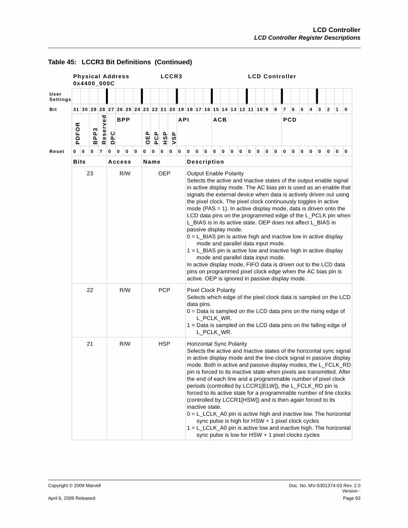
LCD ControllerLCD Controller Register Descriptions
Copyright © 2009 Marvell Doc. No. MV-S301374-03 Rev. 2.0Version -
April 6, 2009 Released Page 93
12345678910111213141516171819202122232425262728293031323334353637383940414243444546474849505152535455565758
23 R/W OEP Output Enable PolaritySelects the active and Inactive states of the output enable signal in active display mode. The AC bias pin is used as an enable that signals the external device when data is actively driven out using the pixel clock. The pixel clock continuously toggles in active mode (PAS = 1). In active display mode, data is driven onto the LCD data pins on the programmed edge of the L_PCLK pin when L_BIAS is in its active state. OEP does not affect L_BIAS in passive display mode.0 = L_BIAS pin is active high and inactive low in active display
mode and parallel data input mode.1 = L_BIAS pin is active low and inactive high in active display
mode and parallel data input mode.In active display mode, FIFO data is driven out to the LCD data pins on programmed pixel clock edge when the AC bias pin is active. OEP is ignored in passive display mode.
22 R/W PCP Pixel Clock PolaritySelects which edge of the pixel clock data is sampled on the LCD data pins.0 = Data is sampled on the LCD data pins on the rising edge of
L_PCLK_WR.1 = Data is sampled on the LCD data pins on the falling edge of
L_PCLK_WR.
21 R/W HSP Horizontal Sync PolaritySelects the active and Inactive states of the horizontal sync signal in active display mode and the line clock signal in passive display mode. Both in active and passive display modes, the L_FCLK_RD pin is forced to its inactive state when pixels are transmitted. After the end of each line and a programmable number of pixel clock periods (controlled by LCCR1[ELW]), the L_FCLK_RD pin is forced to its active state for a programmable number of line clocks (controlled by LCCR1[HSW]) and is then again forced to its inactive state.0 = L_LCLK_A0 pin is active high and inactive low. The horizontal
sync pulse is high for HSW + 1 pixel clock cycles1 = L_LCLK_A0 pin is active low and inactive high. The horizontal
sync pulse is low for HSW + 1 pixel clocks cycles
Table 45: LCCR3 Bit Definitions (Continued)
Physical Address0x4400_000C
LCCR3 LCD Control ler
User Settings
Bit 31 30 29 28 27 26 25 24 23 22 21 20 19 18 17 16 15 14 13 12 11 10 9 8 7 6 5 4 3 2 1 0
PD
FO
R
BP
P3
Re
se
rve
d
DP
CBPP
OE
P
PC
P
HS
P
VS
P
API ACB PCD
Reset 0 0 0 ? 0 0 0 0 0 0 0 0 0 0 0 0 0 0 0 0 0 0 0 0 0 0 0 0 0 0 0 0
Bits Access Name Description

PXA3xx (88AP3xx) Processor FamilyVolume III: Graphics and Input Controller Configuration Developers Manual
Doc. No. MV-S301374-03 Rev. 2.0 Version -
Copyright © 2009 Marvell
Page 94 April 6, 2009 Released
12345678910111213141516171819202122232425262728293031323334353637383940414243444546474849505152535455565758
20 R/W VSP Vertical Sync PolaritySelects the active and inactive states of the vertical sync signal in active display mode, and the frame clock signal in passive display mode. In active display mode, the L_FCLK_RD pin is forced to its inactive state while pixels are transmitted during the frame. After the end of the frame and a programmable number of line clocks periods (controlled by LCCR2[EFW]), the L_FCLK_RD pin is forced to its active state for a programmable number of line clocks (controlled by LCCR2[VSW]), and then is again forced to its inactive state. In passive display mode, the L_FCLK_RD pin is forced to its inactive state while the second line of each frame is transmitted to the end of the frame. The frame clock is then forced to its active state on the rising edge of the first pixel clock of each frame. The frame clock remains active while the entire first line of pixels in the frame is transmitted. Then the clock forced back to its inactive state on the rising edge of the first pixel clock of the second line of the frame.0 = L_FCLK_RD pin is active high and inactive low. The vertical
sync pulse is high for VSW+1 HSYNC clock cycles1 = L_FCLK_RD pin is active low and inactive high. The vertical
sync pulse is low for VSW+1 HSYNC clock cycles.
Table 45: LCCR3 Bit Definitions (Continued)
Physical Address0x4400_000C
LCCR3 LCD Control ler
User Settings
Bit 31 30 29 28 27 26 25 24 23 22 21 20 19 18 17 16 15 14 13 12 11 10 9 8 7 6 5 4 3 2 1 0
PD
FO
R
BP
P3
Re
se
rve
d
DP
CBPP
OE
P
PC
P
HS
P
VS
P
API ACB PCD
Reset 0 0 0 ? 0 0 0 0 0 0 0 0 0 0 0 0 0 0 0 0 0 0 0 0 0 0 0 0 0 0 0 0
Bits Access Name Description

LCD ControllerLCD Controller Register Descriptions
Copyright © 2009 Marvell Doc. No. MV-S301374-03 Rev. 2.0Version -
April 6, 2009 Released Page 95
12345678910111213141516171819202122232425262728293031323334353637383940414243444546474849505152535455565758
19:16 R/W API AC Bias Pin Transitions per InterruptIn passive mode, specifies the number of L_BIAS pin transitions to count before setting the AC bias count status (ACS) bit in the LCD Controller Status register that signals an interrupt request. After the LCD controller is enabled, the value in API is loaded to a 4-bit down counter and the counter decrements each time the AC bias pin is inverted. When the counter reaches zero, it stops and the AC bias count (LCSR0[ABC]) bit is set. When ABC is set, the 4-bit down counter is reloaded with the value in API and is disabled until ABC is cleared. When the CPU clears ABC, the down counter is enabled and again decrements each time the AC bias pin is inverted. The number of AC bias pin transitions between each interrupt request ranges from 0 to 15. Clearing API disables the AC bias pin transitions per interrupt function.In active mode, L_BIAS is used as an output-enable signal. However, the API interrupt can still be signalled. The ACB bit field can be used to count line clock pulses in active mode. When the programmed number of line clock pulses occurs, an internal signal is transitioned to decrement the 4-bit counter used by the API interrupt logic. When this internal signal transitions the programmed number of times as specified by API, an interrupt is generated. Clear API if the API interrupt function is not required in active mode (PAS = 1).The value from 0 to 15 specifies the number of AC bias pin transitions to count before setting the line count status (ABC) bit to signal an interrupt request. The counter is frozen when ABC is set and is restarted when software clears ABC. This function is disabled when API = 0b0000.
Note: API is ignored for LCD panels with internal frame buffers.
Table 45: LCCR3 Bit Definitions (Continued)
Physical Address0x4400_000C
LCCR3 LCD Control ler
User Settings
Bit 31 30 29 28 27 26 25 24 23 22 21 20 19 18 17 16 15 14 13 12 11 10 9 8 7 6 5 4 3 2 1 0
PD
FO
R
BP
P3
Re
se
rve
d
DP
CBPP
OE
P
PC
P
HS
P
VS
P
API ACB PCD
Reset 0 0 0 ? 0 0 0 0 0 0 0 0 0 0 0 0 0 0 0 0 0 0 0 0 0 0 0 0 0 0 0 0
Bits Access Name Description

PXA3xx (88AP3xx) Processor FamilyVolume III: Graphics and Input Controller Configuration Developers Manual
Doc. No. MV-S301374-03 Rev. 2.0 Version -
Copyright © 2009 Marvell
Page 96 April 6, 2009 Released
12345678910111213141516171819202122232425262728293031323334353637383940414243444546474849505152535455565758
15:8 R/W ACB AC Bias Pin FrequencySpecifies the number of line clock periods to count between each toggle of the AC bias pin (L_BIAS). In passive mode, after the LCD controller is enabled, the value in ACB is loaded to an 8-bit down counter and the counter begins to decrement using the line clock. When the counter reaches zero, it stops, the state of L_BIAS is reversed, and the whole procedure restarts. The number of line clocks between each AC bias pin transition ranges from 1 to 256. Program ACB with the preferred number of line clocks minus one. The LCD panel uses this pin to periodically reverse the polarity of the power supplied to the screen to eliminate D.C. offset. If the LCD panel being controlled has its own internal means of switching its power supply, ACB should be configured to its maximum value to reduce power consumption (0xFF). The ACB bit field has no effect on L_BIAS in active mode. Because the pixel clock toggles continuously in active mode, the AC bias pin is used as an output-enable signal. In active mode, the LCD controller automatically asserts it It when pixel data is driven out to the data pins to signal the display when it can latch pixels using the pixel clock.The value from 0 to 255 specifies the number of line clocks to count before toggling the AC bias pin in passive mode (PAS = 0). ACB is ignored in active mode (PAS = 1).Number of line clocks/toggle of the L_BIAS pin = (ACB+1)
Table 45: LCCR3 Bit Definitions (Continued)
Physical Address0x4400_000C
LCCR3 LCD Control ler
User Settings
Bit 31 30 29 28 27 26 25 24 23 22 21 20 19 18 17 16 15 14 13 12 11 10 9 8 7 6 5 4 3 2 1 0
PD
FO
R
BP
P3
Re
se
rve
d
DP
CBPP
OE
P
PC
P
HS
P
VS
P
API ACB PCD
Reset 0 0 0 ? 0 0 0 0 0 0 0 0 0 0 0 0 0 0 0 0 0 0 0 0 0 0 0 0 0 0 0 0
Bits Access Name Description

LCD ControllerLCD Controller Register Descriptions
Copyright © 2009 Marvell Doc. No. MV-S301374-03 Rev. 2.0Version -
April 6, 2009 Released Page 97
12345678910111213141516171819202122232425262728293031323334353637383940414243444546474849505152535455565758
1.5.5 LCD Controller Control Register 4 (LCCR4)LCCR4, shown in Table 46, contains bit fields to program the constants used to calculate the pixel value for half-transparency and output-drive format. The REOFMx interrupt mask bits defined in this register have values of zero on reset. Therefore, the REOFx interrupts are turned on by default. These bits are not compatible with Marvell PXA27x processors because these mask bits are reserved in the PXA27x processor and are written as zeros. These mask bits must be written to a value of 0b1 to turn off the REOFx interrupts. This is a read/write register. Ignore reads from reserved bits. Write 0b0 to reserved bits.
7:0 R/W PCD Pixel Clock DivisorValue (from 0 to 255). Used along with LCCR4[PCDDIV] for passive and active displays to specify the frequency of the pixel clock based on the LCD/system bus clock (LCLK) frequency. Pixel clock frequency can range from LCLK/2 to LCLK/512, where LCLK is the programmed frequency of the LCD controller/system bus frequency. LCLK can vary from 104 MHz to 208 MHzPixel Clock Frequency = LCLK/2(PCD+1) if LCCR4{PCDDIV] = 0 orPixel Clock Frequency = LCLK/(PCD+1) if LCCR4{PCDDIV] = 1PCD must be programmed with a value of 1 or greater if double pixel-clock mode is enabled or if LCCR4{PCDDIV] is set.For LCD panels with an internal frame buffer, this bit field specifies the command inhibit time between any two consecutive reads or writes to the LCD panel (write/write or read/read or write/read or read/write). Command Inhibit TIme = (PCD+1)*LCD_CLK_PERIOD. Refer to Section 1.4.2 for details on setting PCD for proper performance.
Note: PCD can be changed dynamically when the processor operating point changes.
Table 45: LCCR3 Bit Definitions (Continued)
Physical Address0x4400_000C
LCCR3 LCD Control ler
User Settings
Bit 31 30 29 28 27 26 25 24 23 22 21 20 19 18 17 16 15 14 13 12 11 10 9 8 7 6 5 4 3 2 1 0
PD
FO
R
BP
P3
Re
se
rve
d
DP
CBPP
OE
P
PC
P
HS
P
VS
P
API ACB PCD
Reset 0 0 0 ? 0 0 0 0 0 0 0 0 0 0 0 0 0 0 0 0 0 0 0 0 0 0 0 0 0 0 0 0
Bits Access Name Description

PXA3xx (88AP3xx) Processor FamilyVolume III: Graphics and Input Controller Configuration Developers Manual
Doc. No. MV-S301374-03 Rev. 2.0 Version -
Copyright © 2009 Marvell
Page 98 April 6, 2009 Released
12345678910111213141516171819202122232425262728293031323334353637383940414243444546474849505152535455565758
Table 46: LCCR4 Bit Definitions
Physical Address0x4400_0010
LCCR4 LCD Control ler
User Set tings
Bit 31 30 29 28 27 26 25 24 23 22 21 20 19 18 17 16 15 14 13 12 11 10 9 8 7 6 5 4 3 2 1 0
PX
A3
2x
an
PX
A3
0x
On
ly
PC
DD
IV
Re
se
rve
d
Re
se
rve
d
Re
se
rve
d
Re
se
rve
d
RE
OF
M6
Reserved
PA
L_
FO
R
RE
OF
M5
RE
OF
M4
RE
OF
M3
RE
OF
M2
RE
OF
M1
RE
OF
M0
K3 K2 K1
PX
A3
1x
On
ly
PC
DD
IV
CH
RM
_S
EL
OV
2_
CH
RM
_E
N
OV
1_
CH
RM
_E
N
BA
SE
_C
HR
M_
EN
RE
OF
M6
Reserved
PA
L_
FO
R
RE
OF
M5
RE
OF
M4
RE
OF
M3
RE
OF
M2
RE
OF
M1
RE
OF
M0
K3 K2 K1
Reset 0 0 0 0 0 0 ? ? ? ? ? ? ? ? ? 0 0 0 0 0 0 0 0 0 0 0 0 0 0 0 0 0
Bits Access Name Descript ion
31 R/W PCDDIV PCD Divisor SelectionSelects whether the LCD clock is divided by two in the PCD equation. If PCDDIV is set, the minimum value of LCCR3[PCD] is one. If the divisor (denominator in the equations) is odd, the duty cycle is not 50 percent. PCDDIV is ignored when the LCD controller is configured to control a smart panel0 = Pixel clock = LCLK/2*(PCD+1)1 = Pixel clock = LCLK/(PCD+1)
30 R/W CHRM_SEL Selects a particular pixel color to use as transparency color for base/overlays if the chroma key is enabled. This bit is valid only for RGB565 format.0 = Use 0xF81F as chroma-key color.1 = Use 0x781F as chroma-key color.NOTE: PXA31x Only
— — ReservedNOTE: PXA32x and PXA30x Only
29 R/W OV2_CHRM_EN Enables use of particular pixel color as the transparency color for Overlay L2. This valid only for RGB565 format.0 = Use the normal transparency bit specified in each bit.1 = Use one of the following two colors as transparency colors
for overlay2 depending on the LCCR4[CHRM_SEL].• 0xF81F• 0x781F Depending on CHRM_SEL bit, if the pixel value is equal to either of these colors, that pixel is transparent.NOTE: PXA31x Only
— — ReservedNOTE: PXA32x and PXA30x Only

LCD ControllerLCD Controller Register Descriptions
Copyright © 2009 Marvell Doc. No. MV-S301374-03 Rev. 2.0Version -
April 6, 2009 Released Page 99
12345678910111213141516171819202122232425262728293031323334353637383940414243444546474849505152535455565758
28 R/W OV1_CHRM_EN Enables use of particular pixel color as a transparency color for Overlay1 window. This is valid only for RGB565 format.0 = Use the normal transparency bit specified in each bit.1 = Use the following two colors as transparency colors for
overlay1.• 0xF81F• 0x781F If the pixel value is equal to either of these colors, that pixel is transparent.NOTE: PXA31x Only
— — ReservedNOTE: PXA32x and PXA30x Only
27 R/W BASE_CHRM_EN Enables use of a particular pixel color as a transparency color for the base window. This is valid only for RGB565 format.0 = Use the normal transparency bit specified in each bit.1 = Use the following two colors as transparency colors for base.• 0xF81F• 0x781F If the pixel value is equal to either of these colors, that pixel is transparent.NOTE: PXA31x Only
— — ReservedNOTE: PXA32x and PXA30x Only
Table 46: LCCR4 Bit Definitions (Continued)
Physical Address0x4400_0010
LCCR4 LCD Control ler
User Set tings
Bit 31 30 29 28 27 26 25 24 23 22 21 20 19 18 17 16 15 14 13 12 11 10 9 8 7 6 5 4 3 2 1 0
PX
A3
2x
an
PX
A3
0x
On
ly
PC
DD
IV
Re
se
rve
d
Re
se
rve
d
Re
se
rve
d
Re
se
rve
d
RE
OF
M6
Reserved
PA
L_
FO
R
RE
OF
M5
RE
OF
M4
RE
OF
M3
RE
OF
M2
RE
OF
M1
RE
OF
M0
K3 K2 K1
PX
A3
1x
On
ly
PC
DD
IV
CH
RM
_S
EL
OV
2_
CH
RM
_E
N
OV
1_
CH
RM
_E
N
BA
SE
_C
HR
M_
EN
RE
OF
M6
Reserved
PA
L_
FO
R
RE
OF
M5
RE
OF
M4
RE
OF
M3
RE
OF
M2
RE
OF
M1
RE
OF
M0
K3 K2 K1
Reset 0 0 0 0 0 0 ? ? ? ? ? ? ? ? ? 0 0 0 0 0 0 0 0 0 0 0 0 0 0 0 0 0
Bits Access Name Descript ion

PXA3xx (88AP3xx) Processor FamilyVolume III: Graphics and Input Controller Configuration Developers Manual
Doc. No. MV-S301374-03 Rev. 2.0 Version -
Copyright © 2009 Marvell
Page 100 April 6, 2009 Released
12345678910111213141516171819202122232425262728293031323334353637383940414243444546474849505152535455565758
26 R/W REOFM6 Real End Of Frame mask for command (Channel 6)Masks interrupt requests asserted at the end of the last Descriptor of the frame (when the DMA length of transfer counter decrements to zero and LDCMD6[LSTDES_EN] is not configured to 0b10). Setting REOFM6 does not affect the current state of LCSR0[REOF6] or the ability of the LCD controller to set and clear LCSR0[REOF6]; it only blocks the generation of the interrupt request. 0 = The interrupt is enabled, and when LCSR0[REOF6] is set, an
interrupt request is sent to the interrupt controller. 1 = The interrupt is masked and the interrupt controller ignores
the state of the state of LCSR0[REOF6].
25:17 — — Reserved
16:15 R/W PAL_FOR Palette Data formatSpecifies the data format for the palette data. When the overlays are disabled and the bits per pixel value is less than 16 bits, PAL_FOR = 0b00 is used. When the overlays are enabled, the 25-bit palette data format with transparency bit is used. See Figure 15. The PAL_FOR configuration depends on the data formats:• For 16 bits per pixel data format, PAL_FOR = 0b01• For 18 bits per pixel data forma, PAL_FOR = 0b10• For 24 bits per pixel data format, PAL_FOR=0b11. This specifies the palette data format for the palette RAM:0b00 = 16 bits without transparency bit.0b01 = 25-bit format with transparency for 16 bpp data formats0b10 = 25-bit format with transparency for 18 bpp data formats0b11 = 25-bit format with transparency for 24 bpp data formats
Table 46: LCCR4 Bit Definitions (Continued)
Physical Address0x4400_0010
LCCR4 LCD Control ler
User Set tings
Bit 31 30 29 28 27 26 25 24 23 22 21 20 19 18 17 16 15 14 13 12 11 10 9 8 7 6 5 4 3 2 1 0
PX
A3
2x
an
PX
A3
0x
On
ly
PC
DD
IV
Re
se
rve
d
Re
se
rve
d
Re
se
rve
d
Re
se
rve
d
RE
OF
M6
Reserved
PA
L_
FO
R
RE
OF
M5
RE
OF
M4
RE
OF
M3
RE
OF
M2
RE
OF
M1
RE
OF
M0
K3 K2 K1
PX
A3
1x
On
ly
PC
DD
IV
CH
RM
_S
EL
OV
2_
CH
RM
_E
N
OV
1_
CH
RM
_E
N
BA
SE
_C
HR
M_
EN
RE
OF
M6
Reserved
PA
L_
FO
R
RE
OF
M5
RE
OF
M4
RE
OF
M3
RE
OF
M2
RE
OF
M1
RE
OF
M0
K3 K2 K1
Reset 0 0 0 0 0 0 ? ? ? ? ? ? ? ? ? 0 0 0 0 0 0 0 0 0 0 0 0 0 0 0 0 0
Bits Access Name Descript ion

LCD ControllerLCD Controller Register Descriptions
Copyright © 2009 Marvell Doc. No. MV-S301374-03 Rev. 2.0Version -
April 6, 2009 Released Page 101
12345678910111213141516171819202122232425262728293031323334353637383940414243444546474849505152535455565758
14 R/W REOFM5 Real End Of Frame mask for cursor (Channel 5)Masks interrupt requests asserted at the end of the last Descriptor of the frame (when the DMA length of transfer counter decrements to zero and LDCMD5[LSTDES_EN] is not 0b10). Setting REOFM5 does not affect the current state of LCSR0[REOF5] or the ability of the LCD controller to set and clear LCSR0[REOF5]; it only blocks the generation of the interrupt request.0 = Generates an interrupt at the real end of frame. The state of
LCSR0[REOF5] is sent to the interrupt controller.1 = Real end of frame condition does not generate an interrupt
(LCSR0[REOF5] is ignored)
13 R/W REOFM4 Real End Of Frame mask for Overlay 2/Cr (Channel 4)Masks interrupt requests asserted at the end of the last Descriptor of the frame (when the DMA length of transfer counter decrements to zero and LDCMD4[LSTDES_EN] is not 0b10). Setting REOFM4 does not affect the current state of LCSR0[REOF4] or the ability of the LCD controller to set and clear LCSR0[REOF4]; it only blocks the generation of the interrupt request.0 = Generates an interrupt at the real end of frame. The state of
LCSR0[REOF4] is sent to the interrupt controller.1 = Real end of frame condition does not generate an interrupt
(LCSR0[REOF4] is ignored)
Table 46: LCCR4 Bit Definitions (Continued)
Physical Address0x4400_0010
LCCR4 LCD Control ler
User Set tings
Bit 31 30 29 28 27 26 25 24 23 22 21 20 19 18 17 16 15 14 13 12 11 10 9 8 7 6 5 4 3 2 1 0
PX
A3
2x
an
PX
A3
0x
On
ly
PC
DD
IV
Re
se
rve
d
Re
se
rve
d
Re
se
rve
d
Re
se
rve
d
RE
OF
M6
Reserved
PA
L_
FO
R
RE
OF
M5
RE
OF
M4
RE
OF
M3
RE
OF
M2
RE
OF
M1
RE
OF
M0
K3 K2 K1
PX
A3
1x
On
ly
PC
DD
IV
CH
RM
_S
EL
OV
2_
CH
RM
_E
N
OV
1_
CH
RM
_E
N
BA
SE
_C
HR
M_
EN
RE
OF
M6
Reserved
PA
L_
FO
R
RE
OF
M5
RE
OF
M4
RE
OF
M3
RE
OF
M2
RE
OF
M1
RE
OF
M0
K3 K2 K1
Reset 0 0 0 0 0 0 ? ? ? ? ? ? ? ? ? 0 0 0 0 0 0 0 0 0 0 0 0 0 0 0 0 0
Bits Access Name Descript ion
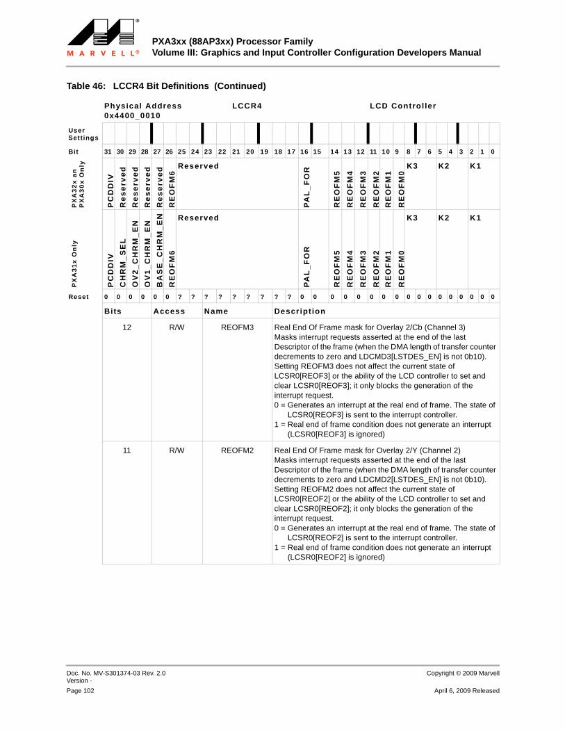
PXA3xx (88AP3xx) Processor FamilyVolume III: Graphics and Input Controller Configuration Developers Manual
Doc. No. MV-S301374-03 Rev. 2.0 Version -
Copyright © 2009 Marvell
Page 102 April 6, 2009 Released
12345678910111213141516171819202122232425262728293031323334353637383940414243444546474849505152535455565758
12 R/W REOFM3 Real End Of Frame mask for Overlay 2/Cb (Channel 3)Masks interrupt requests asserted at the end of the last Descriptor of the frame (when the DMA length of transfer counter decrements to zero and LDCMD3[LSTDES_EN] is not 0b10). Setting REOFM3 does not affect the current state of LCSR0[REOF3] or the ability of the LCD controller to set and clear LCSR0[REOF3]; it only blocks the generation of the interrupt request.0 = Generates an interrupt at the real end of frame. The state of
LCSR0[REOF3] is sent to the interrupt controller.1 = Real end of frame condition does not generate an interrupt
(LCSR0[REOF3] is ignored)
11 R/W REOFM2 Real End Of Frame mask for Overlay 2/Y (Channel 2)Masks interrupt requests asserted at the end of the last Descriptor of the frame (when the DMA length of transfer counter decrements to zero and LDCMD2[LSTDES_EN] is not 0b10). Setting REOFM2 does not affect the current state of LCSR0[REOF2] or the ability of the LCD controller to set and clear LCSR0[REOF2]; it only blocks the generation of the interrupt request.0 = Generates an interrupt at the real end of frame. The state of
LCSR0[REOF2] is sent to the interrupt controller.1 = Real end of frame condition does not generate an interrupt
(LCSR0[REOF2] is ignored)
Table 46: LCCR4 Bit Definitions (Continued)
Physical Address0x4400_0010
LCCR4 LCD Control ler
User Set tings
Bit 31 30 29 28 27 26 25 24 23 22 21 20 19 18 17 16 15 14 13 12 11 10 9 8 7 6 5 4 3 2 1 0
PX
A3
2x
an
PX
A3
0x
On
ly
PC
DD
IV
Re
se
rve
d
Re
se
rve
d
Re
se
rve
d
Re
se
rve
d
RE
OF
M6
Reserved
PA
L_
FO
R
RE
OF
M5
RE
OF
M4
RE
OF
M3
RE
OF
M2
RE
OF
M1
RE
OF
M0
K3 K2 K1
PX
A3
1x
On
ly
PC
DD
IV
CH
RM
_S
EL
OV
2_
CH
RM
_E
N
OV
1_
CH
RM
_E
N
BA
SE
_C
HR
M_
EN
RE
OF
M6
Reserved
PA
L_
FO
R
RE
OF
M5
RE
OF
M4
RE
OF
M3
RE
OF
M2
RE
OF
M1
RE
OF
M0
K3 K2 K1
Reset 0 0 0 0 0 0 ? ? ? ? ? ? ? ? ? 0 0 0 0 0 0 0 0 0 0 0 0 0 0 0 0 0
Bits Access Name Descript ion

LCD ControllerLCD Controller Register Descriptions
Copyright © 2009 Marvell Doc. No. MV-S301374-03 Rev. 2.0Version -
April 6, 2009 Released Page 103
12345678910111213141516171819202122232425262728293031323334353637383940414243444546474849505152535455565758
10 R/W REOFM1 Real End Of Frame mask for Overlay 1 (Channel 1)Masks interrupt requests asserted at the end of the last Descriptor of the frame (when the DMA length of transfer counter decrements to zero and LDCMD1[LSTDES_EN] is not 0b10). Setting REOFM1 does not affect the current state of LCSR0[REOF1] or the ability of the LCD controller to set and clear LCSR0[REOF1]; it only blocks the generation of the interrupt request.0 = Generates an interrupt at the real end of frame. The state of
LCSR0[REOF1] is sent to the interrupt controller.1 = Real end of frame condition does not generate an interrupt
(LCSR0[REOF1] is ignored)
9 R/W REOFM0 Real End Of Frame mask for Base (Channel 0)Masks interrupt requests asserted at the end of the last Descriptor of the frame (when the DMA length of transfer counter decrements to zero and LDCMD0[LSTDES_EN] is not 0b10). Setting REOFM0 does not affect the current state of LCSR0[REOF0] or the ability of the LCD controller to set and clear LCSR0[REOF0]; it only blocks the generation of the interrupt request.0 = Generates an interrupt at the real end of frame. The state of
LCSR0[REOF0] is sent to the interrupt controller.1 = Real end of frame condition does not generate an interrupt
(LCSR0[REOF0] is ignored)
Table 46: LCCR4 Bit Definitions (Continued)
Physical Address0x4400_0010
LCCR4 LCD Control ler
User Set tings
Bit 31 30 29 28 27 26 25 24 23 22 21 20 19 18 17 16 15 14 13 12 11 10 9 8 7 6 5 4 3 2 1 0
PX
A3
2x
an
PX
A3
0x
On
ly
PC
DD
IV
Re
se
rve
d
Re
se
rve
d
Re
se
rve
d
Re
se
rve
d
RE
OF
M6
Reserved
PA
L_
FO
R
RE
OF
M5
RE
OF
M4
RE
OF
M3
RE
OF
M2
RE
OF
M1
RE
OF
M0
K3 K2 K1
PX
A3
1x
On
ly
PC
DD
IV
CH
RM
_S
EL
OV
2_
CH
RM
_E
N
OV
1_
CH
RM
_E
N
BA
SE
_C
HR
M_
EN
RE
OF
M6
Reserved
PA
L_
FO
R
RE
OF
M5
RE
OF
M4
RE
OF
M3
RE
OF
M2
RE
OF
M1
RE
OF
M0
K3 K2 K1
Reset 0 0 0 0 0 0 ? ? ? ? ? ? ? ? ? 0 0 0 0 0 0 0 0 0 0 0 0 0 0 0 0 0
Bits Access Name Descript ion

PXA3xx (88AP3xx) Processor FamilyVolume III: Graphics and Input Controller Configuration Developers Manual
Doc. No. MV-S301374-03 Rev. 2.0 Version -
Copyright © 2009 Marvell
Page 104 April 6, 2009 Released
12345678910111213141516171819202122232425262728293031323334353637383940414243444546474849505152535455565758
8:6 R/W K3 Multiplication Constant for Blue for Half TransparencyHas a value between 1/8 and 1 in increments of 1/8. Program to the appropriate value to get preferred results for half transparency. K3 is used to calculate the results for the blue value. See Section 1.4.4.1 for detailed equations.0b000 = 1/80b001 = 2/80b010 = 3/80b011 = 4/80b100 = 5/80b101 = 6/80b110 = 7/80b111 = 1
5:3 R/W K2 Multiplication Constant for Green for Half TransparencyHas a value between 1/8 and 1 in increments of 1/8. Program to the appropriate value to get preferred results for half transparency. K2 is used to calculate the results for the green value. See Section 1.4.4.1 for detailed equations.0b000 = 1/80b001 =2/80b010 = 3/80b011 = 4/80b100 = 5/80b101 = 6/80b110 =7/80b111 = 1
Table 46: LCCR4 Bit Definitions (Continued)
Physical Address0x4400_0010
LCCR4 LCD Control ler
User Set tings
Bit 31 30 29 28 27 26 25 24 23 22 21 20 19 18 17 16 15 14 13 12 11 10 9 8 7 6 5 4 3 2 1 0
PX
A3
2x
an
PX
A3
0x
On
ly
PC
DD
IV
Re
se
rve
d
Re
se
rve
d
Re
se
rve
d
Re
se
rve
d
RE
OF
M6
Reserved
PA
L_
FO
R
RE
OF
M5
RE
OF
M4
RE
OF
M3
RE
OF
M2
RE
OF
M1
RE
OF
M0
K3 K2 K1
PX
A3
1x
On
ly
PC
DD
IV
CH
RM
_S
EL
OV
2_
CH
RM
_E
N
OV
1_
CH
RM
_E
N
BA
SE
_C
HR
M_
EN
RE
OF
M6
Reserved
PA
L_
FO
R
RE
OF
M5
RE
OF
M4
RE
OF
M3
RE
OF
M2
RE
OF
M1
RE
OF
M0
K3 K2 K1
Reset 0 0 0 0 0 0 ? ? ? ? ? ? ? ? ? 0 0 0 0 0 0 0 0 0 0 0 0 0 0 0 0 0
Bits Access Name Descript ion

LCD ControllerLCD Controller Register Descriptions
Copyright © 2009 Marvell Doc. No. MV-S301374-03 Rev. 2.0Version -
April 6, 2009 Released Page 105
12345678910111213141516171819202122232425262728293031323334353637383940414243444546474849505152535455565758
1.5.6 LCD Controller Control Register 5 (LCCR5)LCCR5, shown in Table 47, contains bit fields to mask interrupt bits for Channel 1 through Channel 6. This is a read/write register. Ignore reads from reserved bits. Write 0b0 to reserved bits.
2:0 R/W K1 Multiplication Constant for Red for Half TransparencyHas a value between 1/8 and 1 in increments of 1/8. Program to the appropriate value to get preferred results for half transparency. K1 is used to calculate the results for the red value. See Section 1.4.4.1 for detailed equations.0b000 = 1/80b001 = 2/80b010 = 3/80b011 = 4/80b100 = 5/80b101 = 6/80b110 = 7/80b111 = 1
Table 46: LCCR4 Bit Definitions (Continued)
Physical Address0x4400_0010
LCCR4 LCD Control ler
User Set tings
Bit 31 30 29 28 27 26 25 24 23 22 21 20 19 18 17 16 15 14 13 12 11 10 9 8 7 6 5 4 3 2 1 0
PX
A3
2x
an
PX
A3
0x
On
ly
PC
DD
IV
Re
se
rve
d
Re
se
rve
d
Re
se
rve
d
Re
se
rve
d
RE
OF
M6
Reserved
PA
L_
FO
R
RE
OF
M5
RE
OF
M4
RE
OF
M3
RE
OF
M2
RE
OF
M1
RE
OF
M0
K3 K2 K1
PX
A3
1x
On
ly
PC
DD
IV
CH
RM
_S
EL
OV
2_
CH
RM
_E
N
OV
1_
CH
RM
_E
N
BA
SE
_C
HR
M_
EN
RE
OF
M6
Reserved
PA
L_
FO
R
RE
OF
M5
RE
OF
M4
RE
OF
M3
RE
OF
M2
RE
OF
M1
RE
OF
M0
K3 K2 K1
Reset 0 0 0 0 0 0 ? ? ? ? ? ? ? ? ? 0 0 0 0 0 0 0 0 0 0 0 0 0 0 0 0 0
Bits Access Name Descript ion
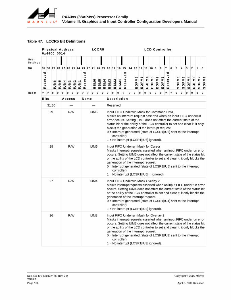
PXA3xx (88AP3xx) Processor FamilyVolume III: Graphics and Input Controller Configuration Developers Manual
Doc. No. MV-S301374-03 Rev. 2.0 Version -
Copyright © 2009 Marvell
Page 106 April 6, 2009 Released
12345678910111213141516171819202122232425262728293031323334353637383940414243444546474849505152535455565758
Table 47: LCCR5 Bit Definitions
Physical Address0x4400_0014
LCCR5 LCD Control ler
User Settings
Bit 31 30 29 28 27 26 25 24 23 22 21 20 19 18 17 16 15 14 13 12 11 10 9 8 7 6 5 4 3 2 1 0
Re
se
rve
d
IUM
6
IUM
5
IUM
4
IUM
3
IUM
2
IUM
1
Re
se
rve
d
BS
M6
BS
M5
BS
M4
BS
M3
BS
M2
BS
M1
Re
se
rve
d
EO
FM
6
EO
FM
5
EO
FM
4
EO
FM
3
EO
FM
2
EO
FM
1
Re
se
rve
d
SO
FM
6
SO
FM
5
SO
FM
4
SO
FM
3
SO
FM
2
SO
FM
1
Reset ? ? 0 0 0 0 0 0 ? ? 0 0 0 0 0 0 ? ? 0 0 0 0 0 0 ? ? 0 0 0 0 0 0
Bits Access Name Descript ion
31:30 — — Reserved
29 R/W IUM6 Input FIFO Underrun Mask for Command DataMasks an interrupt request asserted when an input FIFO underrun error occurs. Setting IUM6 does not affect the current state of the status bit or the ability of the LCD controller to set and clear it; it only blocks the generation of the interrupt request.0 = Interrupt generated (state of LCSR1[IU6] sent to the interrupt
controller).1 = No interrupt (LCSR1[IU6] ignored).
28 R/W IUM5 Input FIFO Underrun Mask for CursorMasks interrupt requests asserted when an input FIFO underrun error occurs. Setting IUM5 does not affect the current state of the status bit or the ability of the LCD controller to set and clear it; it only blocks the generation of the interrupt request.0 = Interrupt generated (state of LCSR1[IU5] sent to the interrupt
controller).1 = No interrupt (LCSR1[IU5] = ignored).
27 R/W IUM4 Input FIFO Underrun Mask Overlay 2Masks interrupt requests asserted when an input FIFO underrun error occurs. Setting IUM4 does not affect the current state of the status bit or the ability of the LCD controller to set and clear it; it only blocks the generation of the interrupt request.0 = Interrupt generated (state of LCSR1[IU4] sent to the interrupt
controller).1 = No interrupt (LCSR1[IU4] ignored).
26 R/W IUM3 Input FIFO Underrun Mask for Overlay 2Masks interrupt requests asserted when an input FIFO underrun error occurs. Setting IUM3 does not affect the current state of the status bit or the ability of the LCD controller to set and clear it; it only blocks the generation of the interrupt request.0 = Interrupt generated (state of LCSR1[IU3] sent to the interrupt
controller).1 = No interrupt (LCSR1[IU3] ignored).
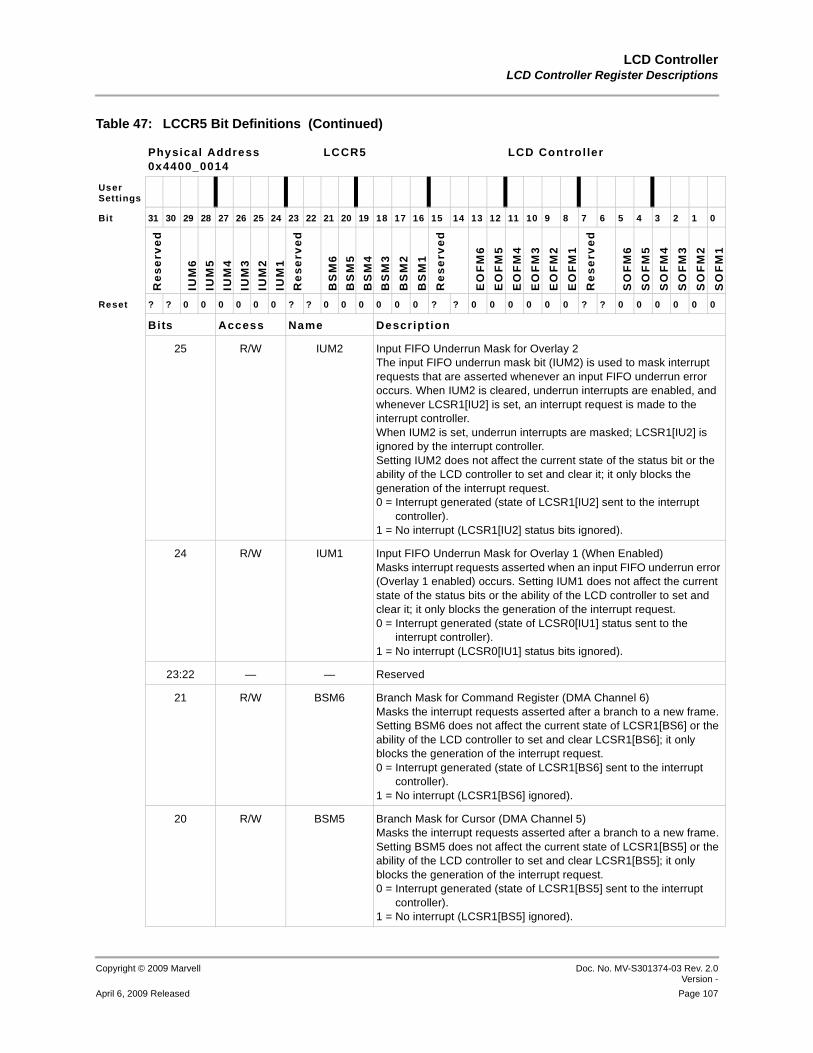
LCD ControllerLCD Controller Register Descriptions
Copyright © 2009 Marvell Doc. No. MV-S301374-03 Rev. 2.0Version -
April 6, 2009 Released Page 107
12345678910111213141516171819202122232425262728293031323334353637383940414243444546474849505152535455565758
25 R/W IUM2 Input FIFO Underrun Mask for Overlay 2The input FIFO underrun mask bit (IUM2) is used to mask interrupt requests that are asserted whenever an input FIFO underrun error occurs. When IUM2 is cleared, underrun interrupts are enabled, and whenever LCSR1[IU2] is set, an interrupt request is made to the interrupt controller. When IUM2 is set, underrun interrupts are masked; LCSR1[IU2] is ignored by the interrupt controller. Setting IUM2 does not affect the current state of the status bit or the ability of the LCD controller to set and clear it; it only blocks the generation of the interrupt request.0 = Interrupt generated (state of LCSR1[IU2] sent to the interrupt
controller).1 = No interrupt (LCSR1[IU2] status bits ignored).
24 R/W IUM1 Input FIFO Underrun Mask for Overlay 1 (When Enabled)Masks interrupt requests asserted when an input FIFO underrun error (Overlay 1 enabled) occurs. Setting IUM1 does not affect the current state of the status bits or the ability of the LCD controller to set and clear it; it only blocks the generation of the interrupt request.0 = Interrupt generated (state of LCSR0[IU1] status sent to the
interrupt controller).1 = No interrupt (LCSR0[IU1] status bits ignored).
23:22 — — Reserved
21 R/W BSM6 Branch Mask for Command Register (DMA Channel 6)Masks the interrupt requests asserted after a branch to a new frame. Setting BSM6 does not affect the current state of LCSR1[BS6] or the ability of the LCD controller to set and clear LCSR1[BS6]; it only blocks the generation of the interrupt request.0 = Interrupt generated (state of LCSR1[BS6] sent to the interrupt
controller).1 = No interrupt (LCSR1[BS6] ignored).
20 R/W BSM5 Branch Mask for Cursor (DMA Channel 5)Masks the interrupt requests asserted after a branch to a new frame. Setting BSM5 does not affect the current state of LCSR1[BS5] or the ability of the LCD controller to set and clear LCSR1[BS5]; it only blocks the generation of the interrupt request.0 = Interrupt generated (state of LCSR1[BS5] sent to the interrupt
controller).1 = No interrupt (LCSR1[BS5] ignored).
Table 47: LCCR5 Bit Definitions (Continued)
Physical Address0x4400_0014
LCCR5 LCD Control ler
User Settings
Bit 31 30 29 28 27 26 25 24 23 22 21 20 19 18 17 16 15 14 13 12 11 10 9 8 7 6 5 4 3 2 1 0
Re
se
rve
d
IUM
6
IUM
5
IUM
4
IUM
3
IUM
2
IUM
1
Re
se
rve
d
BS
M6
BS
M5
BS
M4
BS
M3
BS
M2
BS
M1
Re
se
rve
d
EO
FM
6
EO
FM
5
EO
FM
4
EO
FM
3
EO
FM
2
EO
FM
1
Re
se
rve
d
SO
FM
6
SO
FM
5
SO
FM
4
SO
FM
3
SO
FM
2
SO
FM
1
Reset ? ? 0 0 0 0 0 0 ? ? 0 0 0 0 0 0 ? ? 0 0 0 0 0 0 ? ? 0 0 0 0 0 0
Bits Access Name Descript ion
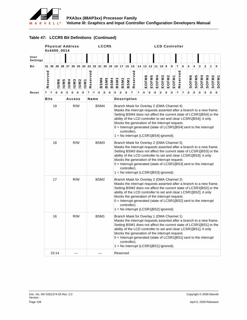
PXA3xx (88AP3xx) Processor FamilyVolume III: Graphics and Input Controller Configuration Developers Manual
Doc. No. MV-S301374-03 Rev. 2.0 Version -
Copyright © 2009 Marvell
Page 108 April 6, 2009 Released
12345678910111213141516171819202122232425262728293031323334353637383940414243444546474849505152535455565758
19 R/W BSM4 Branch Mask for Overlay 2 (DMA Channel 4)Masks the interrupt requests asserted after a branch to a new frame. Setting BSM4 does not affect the current state of LCSR1[BS4] or the ability of the LCD controller to set and clear LCSR1[BS4]; it only blocks the generation of the interrupt request.0 = Interrupt generated (state of LCSR1[BS4] sent to the interrupt
controller).1 = No interrupt (LCSR1[BS4] ignored).
18 R/W BSM3 Branch Mask for Overlay 2 (DMA Channel 3)Masks the interrupt requests asserted after a branch to a new frame. Setting BSM3 does not affect the current state of LCSR1[BS3] or the ability of the LCD controller to set and clear LCSR1[BS3]; it only blocks the generation of the interrupt request.0 = Interrupt generated (state of LCSR1[BS3] sent to the interrupt
controller).1 = No interrupt (LCSR1[BS3] ignored).
17 R/W BSM2 Branch Mask for Overlay 2 (DMA Channel 2)Masks the interrupt requests asserted after a branch to a new frame. Setting BSM2 does not affect the current state of LCSR1[BS2] or the ability of the LCD controller to set and clear LCSR1[BS2]; it only blocks the generation of the interrupt request.0 = Interrupt generated (state of LCSR1[BS2] sent to the interrupt
controller).1 = No interrupt (LCSR1[BS2] ignored).
16 R/W BSM1 Branch Mask for Overlay 1 (DMA Channel 1)Masks the interrupt requests asserted after a branch to a new frame. Setting BSM1 does not affect the current state of LCSR1[BS1] or the ability of the LCD controller to set and clear LCSR1[BS1]; it only blocks the generation of the interrupt request.0 = Interrupt generated (state of LCSR1[BS1] sent to the interrupt
controller).1 = No interrupt (LCSR1[BS1] ignored).
15:14 — — Reserved
Table 47: LCCR5 Bit Definitions (Continued)
Physical Address0x4400_0014
LCCR5 LCD Control ler
User Settings
Bit 31 30 29 28 27 26 25 24 23 22 21 20 19 18 17 16 15 14 13 12 11 10 9 8 7 6 5 4 3 2 1 0
Re
se
rve
d
IUM
6
IUM
5
IUM
4
IUM
3
IUM
2
IUM
1
Re
se
rve
d
BS
M6
BS
M5
BS
M4
BS
M3
BS
M2
BS
M1
Re
se
rve
d
EO
FM
6
EO
FM
5
EO
FM
4
EO
FM
3
EO
FM
2
EO
FM
1
Re
se
rve
d
SO
FM
6
SO
FM
5
SO
FM
4
SO
FM
3
SO
FM
2
SO
FM
1
Reset ? ? 0 0 0 0 0 0 ? ? 0 0 0 0 0 0 ? ? 0 0 0 0 0 0 ? ? 0 0 0 0 0 0
Bits Access Name Descript ion
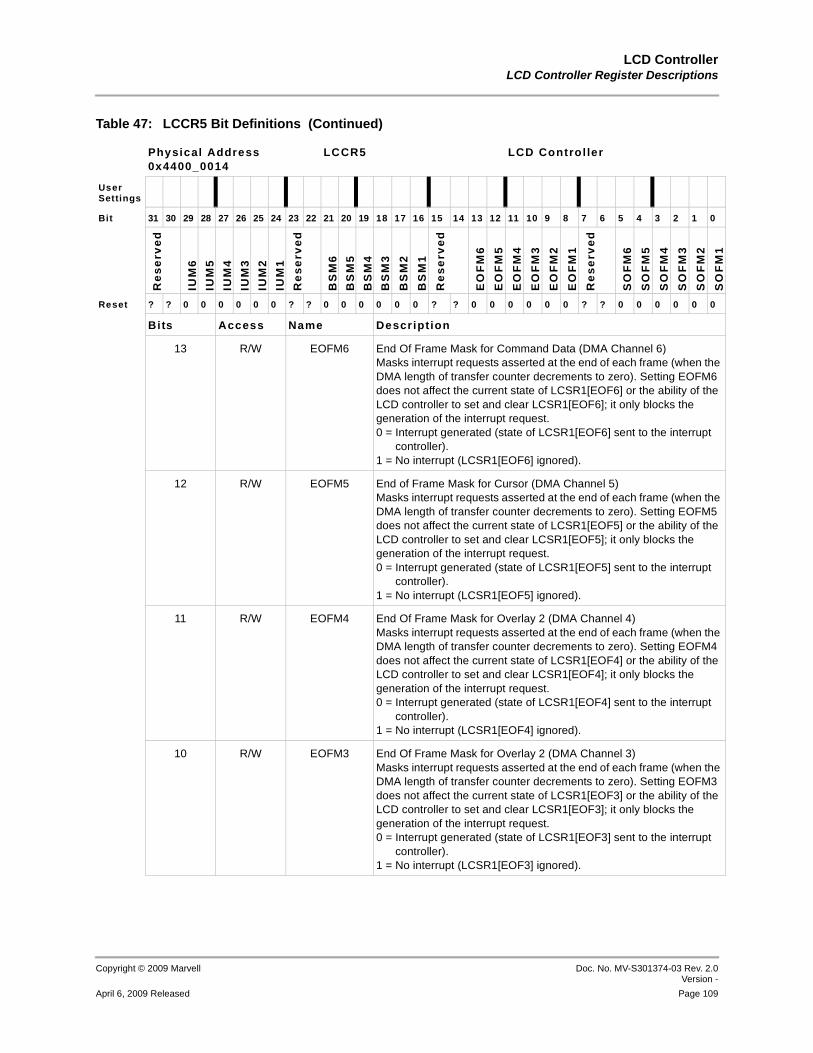
LCD ControllerLCD Controller Register Descriptions
Copyright © 2009 Marvell Doc. No. MV-S301374-03 Rev. 2.0Version -
April 6, 2009 Released Page 109
12345678910111213141516171819202122232425262728293031323334353637383940414243444546474849505152535455565758
13 R/W EOFM6 End Of Frame Mask for Command Data (DMA Channel 6)Masks interrupt requests asserted at the end of each frame (when the DMA length of transfer counter decrements to zero). Setting EOFM6 does not affect the current state of LCSR1[EOF6] or the ability of the LCD controller to set and clear LCSR1[EOF6]; it only blocks the generation of the interrupt request.0 = Interrupt generated (state of LCSR1[EOF6] sent to the interrupt
controller).1 = No interrupt (LCSR1[EOF6] ignored).
12 R/W EOFM5 End of Frame Mask for Cursor (DMA Channel 5)Masks interrupt requests asserted at the end of each frame (when the DMA length of transfer counter decrements to zero). Setting EOFM5 does not affect the current state of LCSR1[EOF5] or the ability of the LCD controller to set and clear LCSR1[EOF5]; it only blocks the generation of the interrupt request.0 = Interrupt generated (state of LCSR1[EOF5] sent to the interrupt
controller).1 = No interrupt (LCSR1[EOF5] ignored).
11 R/W EOFM4 End Of Frame Mask for Overlay 2 (DMA Channel 4)Masks interrupt requests asserted at the end of each frame (when the DMA length of transfer counter decrements to zero). Setting EOFM4 does not affect the current state of LCSR1[EOF4] or the ability of the LCD controller to set and clear LCSR1[EOF4]; it only blocks the generation of the interrupt request.0 = Interrupt generated (state of LCSR1[EOF4] sent to the interrupt
controller).1 = No interrupt (LCSR1[EOF4] ignored).
10 R/W EOFM3 End Of Frame Mask for Overlay 2 (DMA Channel 3)Masks interrupt requests asserted at the end of each frame (when the DMA length of transfer counter decrements to zero). Setting EOFM3 does not affect the current state of LCSR1[EOF3] or the ability of the LCD controller to set and clear LCSR1[EOF3]; it only blocks the generation of the interrupt request.0 = Interrupt generated (state of LCSR1[EOF3] sent to the interrupt
controller).1 = No interrupt (LCSR1[EOF3] ignored).
Table 47: LCCR5 Bit Definitions (Continued)
Physical Address0x4400_0014
LCCR5 LCD Control ler
User Settings
Bit 31 30 29 28 27 26 25 24 23 22 21 20 19 18 17 16 15 14 13 12 11 10 9 8 7 6 5 4 3 2 1 0
Re
se
rve
d
IUM
6
IUM
5
IUM
4
IUM
3
IUM
2
IUM
1
Re
se
rve
d
BS
M6
BS
M5
BS
M4
BS
M3
BS
M2
BS
M1
Re
se
rve
d
EO
FM
6
EO
FM
5
EO
FM
4
EO
FM
3
EO
FM
2
EO
FM
1
Re
se
rve
d
SO
FM
6
SO
FM
5
SO
FM
4
SO
FM
3
SO
FM
2
SO
FM
1
Reset ? ? 0 0 0 0 0 0 ? ? 0 0 0 0 0 0 ? ? 0 0 0 0 0 0 ? ? 0 0 0 0 0 0
Bits Access Name Descript ion

PXA3xx (88AP3xx) Processor FamilyVolume III: Graphics and Input Controller Configuration Developers Manual
Doc. No. MV-S301374-03 Rev. 2.0 Version -
Copyright © 2009 Marvell
Page 110 April 6, 2009 Released
12345678910111213141516171819202122232425262728293031323334353637383940414243444546474849505152535455565758
9 R/W EOFM2 End Of Frame Mask for Overlay 2 (DMA Channel 2)Masks interrupt requests asserted at the end of each frame (when the DMA length of transfer counter decrements to zero). Setting EOFM2 does not affect the current state of LCSR1[EOF2] or the ability of the LCD controller to set and clear LCSR1[EOF2]; it only blocks the generation of the interrupt request.0 = Interrupt generated (state of LCSR1[EOF2] sent to the interrupt
controller).1 = No interrupt (LCSR1[EOF2] ignored).
8 R/W EOFM1 End Of Frame Mask for Overlay 1 (DMA Channel 1)Masks interrupt requests asserted at the end of each frame (when the DMA length of transfer counter decrements to zero). Setting EOFM1 does not affect the current state of LCSR1[EOF1] or the ability of the LCD controller to set and clear LCSR1[EOF1]; it only blocks the generation of the interrupt request.0 = Interrupt generated (state of LCSR1[EOF1] sent to the interrupt
controller).1 = No interrupt (LCSR1[EOF1] ignored).
7:6 — — Reserved
5 R/W SOFM6 Start Of Frame Mask for Command Data (DMA Channel 6)Masks interrupt requests asserted at the beginning of each frame when the LCD frame Descriptor is loaded into the internal DMA registers. Setting SOFM6 does not affect the current state of LCSR1[SOF6] or the ability of the LCD controller to set and clear LCSR1[SOF6]; it only blocks the generation of interrupt requests.0 = Interrupt generated (state of LCSR1[SOF6] sent to the interrupt
controller).1 = No interrupt (LCSR1[SOF6] ignored).
4 R/W SOFM5 Start Of Frame Mask for Cursor (DMA Channel 5)Masks interrupt requests asserted at the beginning of each frame when the LCD frame Descriptor is loaded into the internal DMA registers. Setting SOFM5 does not affect the current state of LCSR1[SOF5] or the ability of the LCD controller to set and clear LCSR1[SOF5]; it only blocks the generation of interrupt requests.0 = Interrupt generated (state of LCSR1[SOF5] sent to the interrupt
controller).1 = No interrupt (LCSR1[SOF5] ignored).
Table 47: LCCR5 Bit Definitions (Continued)
Physical Address0x4400_0014
LCCR5 LCD Control ler
User Settings
Bit 31 30 29 28 27 26 25 24 23 22 21 20 19 18 17 16 15 14 13 12 11 10 9 8 7 6 5 4 3 2 1 0
Re
se
rve
d
IUM
6
IUM
5
IUM
4
IUM
3
IUM
2
IUM
1
Re
se
rve
d
BS
M6
BS
M5
BS
M4
BS
M3
BS
M2
BS
M1
Re
se
rve
d
EO
FM
6
EO
FM
5
EO
FM
4
EO
FM
3
EO
FM
2
EO
FM
1
Re
se
rve
d
SO
FM
6
SO
FM
5
SO
FM
4
SO
FM
3
SO
FM
2
SO
FM
1
Reset ? ? 0 0 0 0 0 0 ? ? 0 0 0 0 0 0 ? ? 0 0 0 0 0 0 ? ? 0 0 0 0 0 0
Bits Access Name Descript ion

LCD ControllerLCD Controller Register Descriptions
Copyright © 2009 Marvell Doc. No. MV-S301374-03 Rev. 2.0Version -
April 6, 2009 Released Page 111
12345678910111213141516171819202122232425262728293031323334353637383940414243444546474849505152535455565758
3 R/W SOFM4 Start Of Frame Mask for Overlay 2 (DMA Channel 4)Masks interrupt requests asserted at the beginning of each frame when the LCD frame Descriptor is loaded into the internal DMA registers. Setting SOFM4 does not affect the current state of LCSR1[SOF4] or the ability of the LCD controller to set and clear LCSR1[SOF4]; it only blocks the generation of interrupt requests.0 = Interrupt generated (state of LCSR1[SOF4] sent to the interrupt
controller).1 = No interrupt (LCSR1[SOF4] ignored).
2 R/W SOFM3 Start Of Frame Mask for Overlay 2 (DMA Channel 3)Masks interrupt requests asserted at the beginning of each frame when the LCD frame Descriptor is loaded into the internal DMA registers. Setting SOFM3 does not affect the current state of LCSR1[SOF3] or the ability of the LCD controller to set and clear LCSR1[SOF3]; it only blocks the generation of interrupt requests.0 = Interrupt generated (state of LCSR1[SOF3] sent to the interrupt
controller).1 = No interrupt (LCSR1[SOF3] ignored).
1 R/W SOFM2 Start Of Frame Mask for Overlay 2 (DMA Channel 2)Masks interrupt requests asserted at the beginning of each frame when the LCD frame Descriptor is loaded into the internal DMA registers. Setting SOFM2 does not affect the current state of LCSR1[SOF2] or the ability of the LCD controller to set and clear LCSR1[SOF2]; it only blocks the generation of interrupt requests.0 = Interrupt generated (state of LCSR1[SOF2] sent to the interrupt
controller).1 = No interrupt (LCSR1[SOF2] ignored).
0 R/W SOFM1 Start Of Frame Mask for Overlay 1 (DMA Channel 1)Masks interrupt requests asserted at the beginning of each frame when the LCD frame Descriptor is loaded into the internal DMA registers. Setting SOFM1 does not affect the current state of LCSR1[SOF1] or the ability of the LCD controller to set and clear LCSR1[SOF1]; it only blocks the generation of interrupt requests.0 = Interrupt generated (state of LCSR1[SOF1] sent to the interrupt
controller).1 = No interrupt (LCSR1[SOF1] ignored).
Table 47: LCCR5 Bit Definitions (Continued)
Physical Address0x4400_0014
LCCR5 LCD Control ler
User Settings
Bit 31 30 29 28 27 26 25 24 23 22 21 20 19 18 17 16 15 14 13 12 11 10 9 8 7 6 5 4 3 2 1 0
Re
se
rve
d
IUM
6
IUM
5
IUM
4
IUM
3
IUM
2
IUM
1
Re
se
rve
d
BS
M6
BS
M5
BS
M4
BS
M3
BS
M2
BS
M1
Re
se
rve
d
EO
FM
6
EO
FM
5
EO
FM
4
EO
FM
3
EO
FM
2
EO
FM
1
Re
se
rve
d
SO
FM
6
SO
FM
5
SO
FM
4
SO
FM
3
SO
FM
2
SO
FM
1
Reset ? ? 0 0 0 0 0 0 ? ? 0 0 0 0 0 0 ? ? 0 0 0 0 0 0 ? ? 0 0 0 0 0 0
Bits Access Name Descript ion

PXA3xx (88AP3xx) Processor FamilyVolume III: Graphics and Input Controller Configuration Developers Manual
Doc. No. MV-S301374-03 Rev. 2.0 Version -
Copyright © 2009 Marvell
Page 112 April 6, 2009 Released
12345678910111213141516171819202122232425262728293031323334353637383940414243444546474849505152535455565758
1.5.7 LCD Controller Control Register 6 (LCCR6)LCCR6 (Table 47) bit fields are used to turn off fetching of the base frame data from the frame buffer and for configuring the constant color value used when the base frame is not fetched from the frame buffer. This register can be updated before the LCD controller is enabled or during normal LCD operation. This is a read/write register. Ignore reads from reserved bits. Write 0b0 to reserved bits.
Table 48: LCCR6 Bit Definitions
Physical Address0x4400_0018
LCCR6 LCD Control ler
User Set tings
Bit 31 30 29 28 27 26 25 24 23 22 21 20 19 18 17 16 15 14 13 12 11 10 9 8 7 6 5 4 3 2 1 0
BF
_O
FF Reserved B_RED B_GREEN B_BLUE
Reset 0 ? ? ? ? ? ? ? 0 0 1 0 0 0 0 0 0 0 0 0 0 0 0 0 0 0 0 0 0 0 0 0
Bits Access Name Descript ion
31 R/W BF_OFF Turn off Fetching Base Frame from Frame BufferWhen set during normal operation, the LCD controller stops fetching the data at the end of the current Descriptor and starts displaying the constant color specified in B_RED, B_GREEN and B_BLUE fields. To enable the base fetching from the frame buffer again, first write the new Descriptor address to FDADR0 with the new address to fetch the base frame data from and then clear BF_OFF.
0 = Base frame is fetched from the frame buffer.1 = Base frame is not fetched from the frame buffer. Instead, the
constant color value specified in the B_RED, B_GREEN, B_BLUE bit fields is used for the entire base.
30:24 — — Reserved
23:16 R/W B_RED Base Red valueSpecifies the constant red value for all pixels in the base frame when the base is not fetched from the frame buffer (BF_OFF set). This bit field is ignored when BF_OFF is cleared.
15:8 R/W B_GREEN Base Green valueSpecifies the constant green value for all pixels in the base frame when the base is not fetched from the frame buffer (BF_OFF set). This bit field is ignored when BF_OFF is cleared.
7:0 R/W B_BLUE Base Blue valueSpecifies the constant blue value for all pixels in the base frame when the base is not fetched from the frame buffer (BF_OFF set). This bit field is ignored when BF_OFF is cleared.

LCD ControllerLCD Controller Register Descriptions
Copyright © 2009 Marvell Doc. No. MV-S301374-03 Rev. 2.0Version -
April 6, 2009 Released Page 113
12345678910111213141516171819202122232425262728293031323334353637383940414243444546474849505152535455565758
1.5.8 Overlay 1 Control Register 1 (OVL1C1)OVL1C1 (Table 49) bit fields enable and set the size and pixel format for the Overlay 1 window. This is a read/write register. Ignore reads from reserved bits. Write 0b0 to reserved bits.
Table 49: OVL1C1 Bit Definitions
Physical Address0x4400_0050
OVL1C1 LCD Control ler
User Set tings
Bit 31 30 29 28 27 26 25 24 23 22 21 20 19 18 17 16 15 14 13 12 11 10 9 8 7 6 5 4 3 2 1 0
O1
EN Reserved BPP1 LPO1 PPL1
Reset 0 ? ? ? ? ? ? ? 0 0 1 0 0 0 0 0 0 0 0 0 0 0 0 0 0 0 0 0 0 0 0 0
Bits Access Name Descript ion
31 R/W O1EN Enable bit for Overlay 1Enables/disables the display of the Overlay 1. 0 = Overlay 1 is disabled.1 = Overlay 1 is enabled.
30:24 — — Reserved
23:20 R/W BPP1 Bits per Pixel for Overlay 1Specifies the pixel depth of each pixel stored in the memory. For a pixel depth of 8 bpp, the internal palette RAM must be loaded before pixels can be displayed on the screen.0b0000 = 24-bit mode without transparency bit. 0b0010 = Reserved0b0011 = 8 bpp [256 entry, 512 or 1024 byte palette buffer]0b0100 = 16 bpp [no palette buffer]0b0101 = 18 bpp unpacked [no palette buffer]0b0110 = 18 bpp packed [no palette buffer]0b0111 = 19 bpp unpacked [no palette buffer]0b1000 = 19 bpp packed [no palette buffer]0b1001 = 24 bpp [no palette buffer]0b1010 = 25 bpp [no palette buffer]0b1011 = 18-bits/pixel in (6R+2’0s, 6G+2’0s, 6B+2’0s) format. (PXA31x Only)0b1100 = 18-bits/pixel packed in (6R+2’0s, 6G+2’0s, 6B+2’0s) format (PXA31x Only)0b1101 = 19-bits/pixel in (6R+2’0s, 6G+2’0s, 6B+2’0s) format (PXA31x Only
0b1011 = Reserved (PXA32x and PXA30x Only)0b1100 = Reserved (PXA32x and PXA30x Only)0b1101 = Reserved (PXA32x and PXA30x Only)Others = ReservedWhen BPP1 = 0x0 Overlay 1 is configured for 24 bpp mode with transparency enabled, and with 8 bits each of red, green and blue. The transparency bit (T) does not exist, but transparency is enabled. Refer to Section 1.4.4.1 on page ii-37 and Section 6 on page ii-38.

PXA3xx (88AP3xx) Processor FamilyVolume III: Graphics and Input Controller Configuration Developers Manual
Doc. No. MV-S301374-03 Rev. 2.0 Version -
Copyright © 2009 Marvell
Page 114 April 6, 2009 Released
12345678910111213141516171819202122232425262728293031323334353637383940414243444546474849505152535455565758
1.5.9 Overlay 1 Control Register 2 (OVL1C2)OVL1C2, shown in Table 50, contains bit fields that are programmed to set the position of Overlay 1 on the panel display. This is a read/write register. Ignore reads from reserved bits. Write 0b0 to reserved bits.
19:10 R/W LPO1 Number of Lines for Overlay 1Specifies the number line or rows present in the Overlay 1 frame. This also represents the size of the overlay in the vertical direction. LPO1 is a 10-bit value that represents between 10 and 640 lines per screen. This specifies the size of the Overlay 1 window in the vertical direction. This is programmed with the value from 9 to 639. Actual number of line = LPO1 +1
9:0 R/W PPL1 Pixels per Line for Overlay 1 frameSpecifies the number of pixels in each line or row for the Overlay 1 frame. PPL1 is a 10-bit value that represents between 10 and 640 pixels per line. See Section 1.4.12 for the restrictions on pixels per line. Value (from 9 to 639). Used to specify number of pixel contained within each line for the Overlay 1 frame. Actual pixel per line = (PPL1 +1)
Table 49: OVL1C1 Bit Definitions (Continued)
Physical Address0x4400_0050
OVL1C1 LCD Control ler
User Set tings
Bit 31 30 29 28 27 26 25 24 23 22 21 20 19 18 17 16 15 14 13 12 11 10 9 8 7 6 5 4 3 2 1 0
O1
EN Reserved BPP1 LPO1 PPL1
Reset 0 ? ? ? ? ? ? ? 0 0 1 0 0 0 0 0 0 0 0 0 0 0 0 0 0 0 0 0 0 0 0 0
Bits Access Name Descript ion
Table 50: OVL1C2 Bit Definitions
Physical Address0x4400_0060
OVL1C2 LCD Control ler
User Set tings
Bit 31 30 29 28 27 26 25 24 23 22 21 20 19 18 17 16 15 14 13 12 11 10 9 8 7 6 5 4 3 2 1 0
Reserved O1YPOS O1XPOS
Reset ? ? ? ? ? ? ? ? ? ? ? ? 0 0 0 0 0 0 0 0 0 0 0 0 0 0 0 0 0 0 0 0
Bits Access Name Description
31:20 — — Reserved
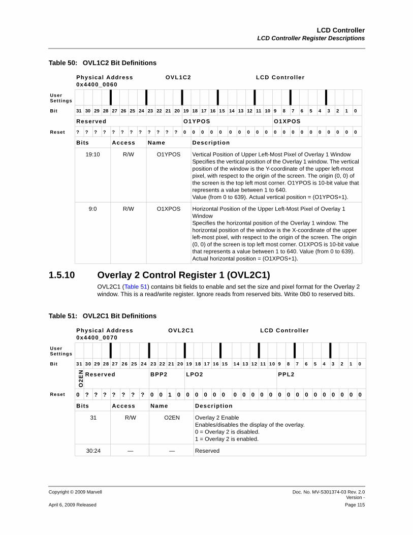
LCD ControllerLCD Controller Register Descriptions
Copyright © 2009 Marvell Doc. No. MV-S301374-03 Rev. 2.0Version -
April 6, 2009 Released Page 115
12345678910111213141516171819202122232425262728293031323334353637383940414243444546474849505152535455565758
1.5.10 Overlay 2 Control Register 1 (OVL2C1)OVL2C1 (Table 51) contains bit fields to enable and set the size and pixel format for the Overlay 2 window. This is a read/write register. Ignore reads from reserved bits. Write 0b0 to reserved bits.
19:10 R/W O1YPOS Vertical Position of Upper Left-Most Pixel of Overlay 1 WindowSpecifies the vertical position of the Overlay 1 window. The vertical position of the window is the Y-coordinate of the upper left-most pixel, with respect to the origin of the screen. The origin (0, 0) of the screen is the top left most corner. O1YPOS is 10-bit value that represents a value between 1 to 640.Value (from 0 to 639). Actual vertical position = (O1YPOS+1).
9:0 R/W O1XPOS Horizontal Position of the Upper Left-Most Pixel of Overlay 1 WindowSpecifies the horizontal position of the Overlay 1 window. The horizontal position of the window is the X-coordinate of the upper left-most pixel, with respect to the origin of the screen. The origin (0, 0) of the screen is top left most corner. O1XPOS is 10-bit value that represents a value between 1 to 640. Value (from 0 to 639). Actual horizontal position = (O1XPOS+1).
Table 50: OVL1C2 Bit Definitions
Physical Address0x4400_0060
OVL1C2 LCD Control ler
User Set tings
Bit 31 30 29 28 27 26 25 24 23 22 21 20 19 18 17 16 15 14 13 12 11 10 9 8 7 6 5 4 3 2 1 0
Reserved O1YPOS O1XPOS
Reset ? ? ? ? ? ? ? ? ? ? ? ? 0 0 0 0 0 0 0 0 0 0 0 0 0 0 0 0 0 0 0 0
Bits Access Name Description
Table 51: OVL2C1 Bit Definitions
Physical Address0x4400_0070
OVL2C1 LCD Control ler
User Settings
Bit 31 30 29 28 27 26 25 24 23 22 21 20 19 18 17 16 15 14 13 12 11 10 9 8 7 6 5 4 3 2 1 0
O2
EN Reserved BPP2 LPO2 PPL2
Reset 0 ? ? ? ? ? ? ? 0 0 1 0 0 0 0 0 0 0 0 0 0 0 0 0 0 0 0 0 0 0 0 0
Bits Access Name Descript ion
31 R/W O2EN Overlay 2 EnableEnables/disables the display of the overlay. 0 = Overlay 2 is disabled.1 = Overlay 2 is enabled.
30:24 — — Reserved

PXA3xx (88AP3xx) Processor FamilyVolume III: Graphics and Input Controller Configuration Developers Manual
Doc. No. MV-S301374-03 Rev. 2.0 Version -
Copyright © 2009 Marvell
Page 116 April 6, 2009 Released
12345678910111213141516171819202122232425262728293031323334353637383940414243444546474849505152535455565758
23:20 R/W BPP2 Bits per Pixel for Overlay 2Specifies the pixel depth of each pixel stored in the internal or the external memory for the Overlay 2 frame. Pixel depth of 8 bpp requires the internal palette RAM be loaded before pixels can be displayed on the screen. 0b0010 = Reserved0b0011 = 8 bpp [256 entry, 512 or 1024 byte palette buffer]0b0100 = 16 bpp [no palette buffer]0b0101 = 18 bpp, unpacked [no palette buffer]0b0110 = 18 bpp, packed [no palette buffer]0b0111 = 19 bpp, unpacked [no palette buffer]0b1000 = 19 bpp, packed [no palette buffer]0b1001 = 24 bpp [no palette buffer]0b1010 = 25 bpp [no palette buffer]0b1011 = 18-bits/pixel in (6R+2’0s, 6G+2’0s, 6B+2’0s) format (PXA31x Only)0b1100 = 18-bits/pixel packed in (6R+2’0s, 6G+2’0s, 6B+2’0s) format (PXA31x Only)0b1101 = 19-bits/pixel in (6R+2’0s, 6G+2’0s, 6B+2’0s) format (PXA31x Only)0b1011 = Reserved (PXA32x and PXA30x Only)0b1100 = Reserved (PXA32x and PXA30x Only)0b1101 = Reserved (PXA32x and PXA30x Only)others = Reserved
19:10 R/W LPO2 Number of Lines for Overlay 2 FrameSpecifies the number line or rows in the Overlay 2 frame and also represents the size of the overlay in the vertical direction. LPO2[9:0] represents a value between 10 and 640 lines per screen to specify the size of the Overlay 2 frame in the vertical direction. This field is programmed with the value from 9 to 639. The actual number of line = LPO2 +1. If YCbCr 4:2:0 planar format is selected, LPO2 must be > 1.
9:0 R/W PPL2 Pixel per Line for Overlay 2 FrameSpecifies the number of pixels in each line or row for the Overlay 2 frame. PPL2[9:0] represents a value between 10 and 640 pixels per line. See Section 1.4.12 for the restrictions on pixels per line.The value represented is from 9 to 639. Actual pixel per line = (PPL2+1).If YCbCr 4:2:2 or 4:2:0 Planar formats are selected, PPL2 must be > 15 and multiples of 16.
Table 51: OVL2C1 Bit Definitions (Continued)
Physical Address0x4400_0070
OVL2C1 LCD Control ler
User Settings
Bit 31 30 29 28 27 26 25 24 23 22 21 20 19 18 17 16 15 14 13 12 11 10 9 8 7 6 5 4 3 2 1 0
O2
EN Reserved BPP2 LPO2 PPL2
Reset 0 ? ? ? ? ? ? ? 0 0 1 0 0 0 0 0 0 0 0 0 0 0 0 0 0 0 0 0 0 0 0 0
Bits Access Name Descript ion

LCD ControllerLCD Controller Register Descriptions
Copyright © 2009 Marvell Doc. No. MV-S301374-03 Rev. 2.0Version -
April 6, 2009 Released Page 117
12345678910111213141516171819202122232425262728293031323334353637383940414243444546474849505152535455565758
1.5.11 Overlay 2 Control Register 2 (OVL2C2)Overlay 2 Control register 2 (OVL2C2) (Table 52) contains bit fields that are programmed to set the format of the pixel data and the position of Overlay 2 on the panel display. This is a read/write register. Ignore reads from reserved bits. Write 0b0 to reserved bits.
1.5.12 Cursor Control Register (CCR)CCR, shown in Table 53, contains bit fields to enable, configure, and set the position of the hardware cursor. This is a read/write register. Ignore reads from reserved bits. Write 0b0 to reserved bits.
Table 52: OVL2C2 Bit Definitions
Physical Address0x4400_0080
OVL2C2 LCD Control ler
User Settings
Bit 31 30 29 28 27 26 25 24 23 22 21 20 19 18 17 16 15 14 13 12 11 10 9 8 7 6 5 4 3 2 1 0
Reserved FOR O2YPOS O2XPOS
Reset ? ? ? ? ? ? ? ? ? 0 0 0 0 0 0 0 0 0 0 0 0 0 0 0 0 0 0 0 0 0 0 0
Bits Access Name Descript ion
31:23 — — Reserved
22:20 R/W FOR Format.Specifies the format of the pixel data for Overlay 2. The pixel data can be in RGB or YCbCr format as shown below.Specifies the data format stored in the memory0b000 - RGB0b001 - YCbCr 4:4:4 Packed0b010 - YCbCr 4:4:4 Planar0b011 - YCbCr 4:2:2 Planar0b100 - YCbCr 4:2:0 PlanarOthers - Reserved
Note:
19:10 R/W O2YPOS Vertical Position of the Upper Left Most Pixel of Overlay 2.Specifies the vertical position of the Overlay 2 frame. The vertical position of the Overlay 2 frame is the Y-coordinate of the upper left-most pixel, with respect to the origin of the screen. O2YPOS[9:0] represents a value between 1 and 640. Value is between 0 and 639. The origin (0, 0) of the screen is top left most corner.
9:0 R/W O2XPOS Horizontal Position of the Upper Leftmost Pixel of Overlay 2.Specifies the horizontal position of the Overlay 2 frame. The horizontal position of the frame is the X-coordinate of the upper left-most pixel, with respect to the origin of the screen. O2XPOS[9:0] represents a value between 1 to 640. Value is between 0 to 639. The origin (0, 0) of the screen is top leftmost corner.

PXA3xx (88AP3xx) Processor FamilyVolume III: Graphics and Input Controller Configuration Developers Manual
Doc. No. MV-S301374-03 Rev. 2.0 Version -
Copyright © 2009 Marvell
Page 118 April 6, 2009 Released
12345678910111213141516171819202122232425262728293031323334353637383940414243444546474849505152535455565758
1.5.13 Command Control Register (CMDCR)CMDCR, shown in Table 54, contains bit fields to program the counter values used for synchronization when interfacing the LCD panels with the internal frame buffer. This is a read/write register. Ignore reads from reserved bits. Write 0b0 to reserved bits.
Table 53: CCR Bit Definitions
Physical Address0x4400_0090
CCR LCD Control ler
User Settings
Bit 31 30 29 28 27 26 25 24 23 22 21 20 19 18 17 16 15 14 13 12 11 10 9 8 7 6 5 4 3 2 1 0
CE
N
Reserved CYPOS CXPOS
Re
se
rve
d CURMS
Reset 0 ? ? ? ? ? ? 0 0 0 0 0 0 0 0 0 0 0 0 0 0 0 0 0 0 0 0 ? 0 0 0
Bits Access Name Descript ion
31 R/W CEN Cursor EnableEnables the hardware cursor. 0 = Hardware cursor disabled1 = Hardware cursor enabled
30:25 — — Reserved
24:15 R/W CYPOS Vertical Position of the CursorSpecifies the Y-coordinates of the upper-left corner pixel of the cursor. CYPOS is 10-bit value from 0 to 799.
14:5 R/W CXPOS Horizontal Position of the CursorSpecifies the X-coordinates of the upper-left corner pixel of the cursor. CXPOS is 10-bit value from 0 to 799.
4:3 — — Reserved
2:0 R/W CURMS Cursor Mode SelectSelects one of the six available cursor modes.0b000 = 32x32x2 bpp 2-color and Transparency mode0b001 = 32x32x2 bpp 3-color and Transparency mode0b010 = 32x32x2 bpp 4-color mode0b011 = 64x64x2 bpp 2-color and Transparency mode0b100 = 64x64x2 bpp 3-color and Transparency mode0b101 = 64x64x2 bpp 4-color mode.0b110 = 128x128x1 bpp 2-color mode0b111 = 128x128x1 bpp 1-color and Transparency mode
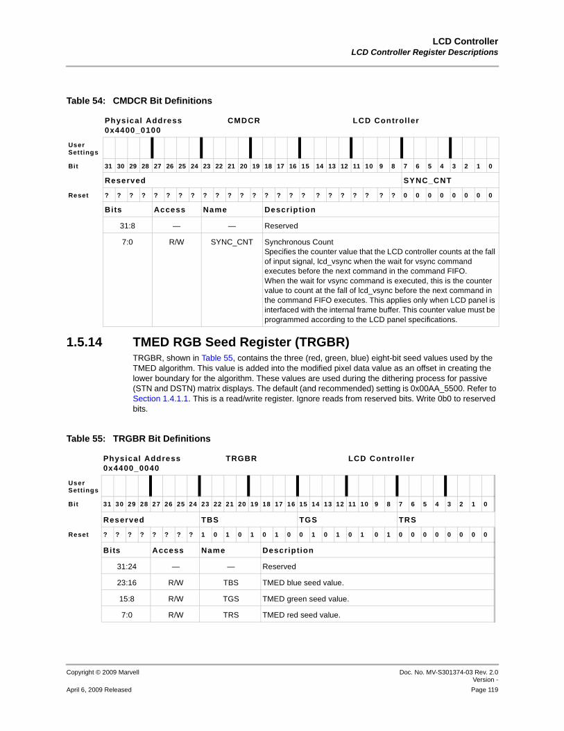
LCD ControllerLCD Controller Register Descriptions
Copyright © 2009 Marvell Doc. No. MV-S301374-03 Rev. 2.0Version -
April 6, 2009 Released Page 119
12345678910111213141516171819202122232425262728293031323334353637383940414243444546474849505152535455565758
1.5.14 TMED RGB Seed Register (TRGBR)TRGBR, shown in Table 55, contains the three (red, green, blue) eight-bit seed values used by the TMED algorithm. This value is added into the modified pixel data value as an offset in creating the lower boundary for the algorithm. These values are used during the dithering process for passive (STN and DSTN) matrix displays. The default (and recommended) setting is 0x00AA_5500. Refer to Section 1.4.1.1. This is a read/write register. Ignore reads from reserved bits. Write 0b0 to reserved bits.
Table 54: CMDCR Bit Definitions
Physical Address0x4400_0100
CMDCR LCD Control ler
User Set tings
Bit 31 30 29 28 27 26 25 24 23 22 21 20 19 18 17 16 15 14 13 12 11 10 9 8 7 6 5 4 3 2 1 0
Reserved SYNC_CNT
Reset ? ? ? ? ? ? ? ? ? ? ? ? ? ? ? ? ? ? ? ? ? ? ? ? 0 0 0 0 0 0 0 0
Bits Access Name Description
31:8 — — Reserved
7:0 R/W SYNC_CNT Synchronous CountSpecifies the counter value that the LCD controller counts at the fall of input signal, lcd_vsync when the wait for vsync command executes before the next command in the command FIFO. When the wait for vsync command is executed, this is the counter value to count at the fall of lcd_vsync before the next command in the command FIFO executes. This applies only when LCD panel is interfaced with the internal frame buffer. This counter value must be programmed according to the LCD panel specifications.
Table 55: TRGBR Bit Definitions
Physical Address0x4400_0040
TRGBR LCD Control ler
User Settings
Bit 31 30 29 28 27 26 25 24 23 22 21 20 19 18 17 16 15 14 13 12 11 10 9 8 7 6 5 4 3 2 1 0
Reserved TBS TGS TRS
Reset ? ? ? ? ? ? ? ? 1 0 1 0 1 0 1 0 0 1 0 1 0 1 0 1 0 0 0 0 0 0 0 0
Bits Access Name Description
31:24 — — Reserved
23:16 R/W TBS TMED blue seed value.
15:8 R/W TGS TMED green seed value.
7:0 R/W TRS TMED red seed value.

PXA3xx (88AP3xx) Processor FamilyVolume III: Graphics and Input Controller Configuration Developers Manual
Doc. No. MV-S301374-03 Rev. 2.0 Version -
Copyright © 2009 Marvell
Page 120 April 6, 2009 Released
12345678910111213141516171819202122232425262728293031323334353637383940414243444546474849505152535455565758
1.5.15 TMED Control Register (TCR)TCR, shown in Table 56, selects the options available to use a patented temporal modulated energy-distribution (TMED) algorithm. This algorithm is used to improve image quality on STN (passive) panels.Two TMED algorithms can be used. The default (and recommended) setting is 0x0000_754F. This is a read/write register. Ignore reads from reserved bits. Write 0b0 to reserved bits.
Table 56: TCR Bit Definitions
Physical Address0x4400_0030
TCR LCD Controller
User Settings
Bit 31 30 29 28 27 26 25 24 23 22 21 20 19 18 17 16 15 14 13 12 11 10 9 8 7 6 5 4 3 2 1 0
Reserved
TE
D
TSCS
THBS TVBS
TM
1E
N
TM
2E
N
TM
1S
TM
2S
Reset ? ? ? ? ? ? ? ? ? ? ? ? ? ? ? ? ? 1 1 1 0 1 0 1 0 1 0 0 1 1 1 1
Bits Access Name Descript ion
31:15 — — Reserved
14 R/W TED TMED Energy Distribution SelectSelects which matrix is used in the final step of the TMED algorithm. Setting TED selects the (preferred) TMED2 matrix, and clearing it selects the older TMED matrix. After the pixel value goes through the algorithm to determine a lower and upper boundary, the row and column counters are combined and run through one of the matrices to obtain a number that is compared to the two boundaries. If that number is between the two boundaries, then the data out for this pixel in this frame is a 1. Otherwise, it is a 0.0 = Selects scheme 1.1 = Selects scheme 2.
13:12 R/W TSCS TMED Shades per Color SelectAllows software to adjust the value of the incoming pixel by rounding off the 1, 2, or 3 least significant bits. This adjusted value is then used in both the color-offset adjuster and as the pixel value in the multiplication step of the TMED algorithm. The shades per color (distinct pixel values) can then be reduced to 33, 65, or 129; or remain at 256.0b00 = 33 shades for red, 65 shades for green, and 33 shades for blue.0b01 = 65 shades for red, blue, and green.0b10 = 129 shades for red, blue, and green.0b11 = 256 shades for red, blue, and green.
11:8 R/W THBS TMED Horizontal Beat SuppressionSpecifies the column shift value.The column-shift is used as an offset that is combined with the row (line) counter and the pixel counter to create an address to look up in the matrix. The matrix output is compared to the upper and lower boundaries defined in Section 1.4.1.1.

LCD ControllerLCD Controller Register Descriptions
Copyright © 2009 Marvell Doc. No. MV-S301374-03 Rev. 2.0Version -
April 6, 2009 Released Page 121
12345678910111213141516171819202122232425262728293031323334353637383940414243444546474849505152535455565758
7:4 R/W TVBS TMED Vertical Beat SuppressionSpecifies the block shift value. The block shift is used as an offset that is combined with the pixel counter.
3 R/W TM1EN TMED Method 1 EnableThe frame shift enable bit that allows the frame-number adjuster to add an offset to the current frame number before the value is sent through the algorithm. Setting this bit enables the addition of the current frame number to a value composed from the row and column counters. This value is derived from one of the two lookup matrices, which is selected by bit 1 (TMED Method 1 Select).0 = Disables scheme 1.1 = Enables scheme 2.
2 R/W TM2EN TMED Method 2 EnableEnables the color-offset adjuster for each color. The color-offset adjuster creates the offset in the lower boundary in the TMED algorithm (the formula is: LB = PixelValue X FrameNumber + Offset). The offset is created by adding either the output of the lookup matrix (input was the color value) or 00 to the seed value in the TSR for that color. The color-offset adjuster for each color can be disabled by clearing this bit. When cleared, this bit selects only the Seed register value to go through the algorithm.0 = Disables scheme 1.1 = Enables scheme 2.
1 R/W TM1S TMED Method 1 SelectSelects which matrix is used with the frame-number adjuster. A 1 selects the (preferred) TMED2 matrix, and a 0 selects the older TMED matrix.0 = Selects scheme 1.1 = Selects scheme 2.
0 R/W TM2S TMED Method 2 SelectSelects which matrix is used with the color-offset adjuster. A 1 selects the (preferred) TMED2 matrix, and a 0 selects the older TMED matrix.0 = Selects scheme 1.1 = Selects scheme 2.
Table 56: TCR Bit Definitions (Continued)
Physical Address0x4400_0030
TCR LCD Controller
User Settings
Bit 31 30 29 28 27 26 25 24 23 22 21 20 19 18 17 16 15 14 13 12 11 10 9 8 7 6 5 4 3 2 1 0
Reserved
TE
D
TSCS
THBS TVBS
TM
1E
N
TM
2E
N
TM
1S
TM
2S
Reset ? ? ? ? ? ? ? ? ? ? ? ? ? ? ? ? ? 1 1 1 0 1 0 1 0 1 0 0 1 1 1 1
Bits Access Name Descript ion

PXA3xx (88AP3xx) Processor FamilyVolume III: Graphics and Input Controller Configuration Developers Manual
Doc. No. MV-S301374-03 Rev. 2.0 Version -
Copyright © 2009 Marvell
Page 122 April 6, 2009 Released
12345678910111213141516171819202122232425262728293031323334353637383940414243444546474849505152535455565758
1.5.16 DMA Frame Descriptor Address Registers (FDADRx)FDADRx, shown in Table 57, contain the memory address of the next Descriptor for that channel. The DMA controller fetches the Descriptor at this location after finishing the current Descriptor. The bits in this register are undefined on powerup. The Descriptor address must be aligned to a 128-bit (16-byte) boundary; therefore, bits [3:0] of the address are reserved. These are read/write registers. Ignore reads from reserved bits. Write 0b0 to reserved bits.
1.5.17 DMA Frame Branch Registers (FBRx)FBRx, shown in Table 58, contain the address of the Descriptor to which to branch (aligned on a 4-byte boundary). When this register is written and BRA = 1, the Frame Descriptor Address register (FDADR) is ignored and the next Descriptor is fetched from the address in this register. Setting BINT = 1 tells the DMA controller to set the branch-status interrupt bit (BS) in the LCD Controller Status register after fetching the branched-to Descriptor. Hardware automatically clears BRA when the branch is taken. This is a read/write register. Ignore reads from reserved bits. Write 0b0 to reserved bits.
Table 57: FDADR0/1/2/3/4/5/6 Bit Definitions
Physical Address0x4400_02000x4400_02100x4400_02200x4400_02300x4400_02400x4400_02500x4400_0260
FDADR0FDADR1FDADR2FDADR3FDADR4FDADR5FDADR6
LCD Control ler
User Settings
Bit 31 30 29 28 27 26 25 24 23 22 21 20 19 18 17 16 15 14 13 12 11 10 9 8 7 6 5 4 3 2 1 0
DESCRIPTOR ADDRESS Reserved
Reset 0 0- 0 0 0 0 0 0 0 0 0 0 0 0 0 0 0 0 0 0 0 0 0 0 0 0 0 0 ? ? ? ?
Bits Access Name Descript ion
31:4 R/W DESCRIPTOR ADDRESS
Descriptor addressAddress of next Descriptor
3:0 — — Reserved

LCD ControllerLCD Controller Register Descriptions
Copyright © 2009 Marvell Doc. No. MV-S301374-03 Rev. 2.0Version -
April 6, 2009 Released Page 123
12345678910111213141516171819202122232425262728293031323334353637383940414243444546474849505152535455565758
1.5.18 Panel Read Status Register (PRSR)PRSR, shown in Table 59, contains bit fields to load the read data from the LCD panel by the LCD controller and the status bits. This register is valid only when the LCD controller is configured to operate with smart panels. This is a read/write register. Ignore reads from reserved bits. Write 0b0 to reserved bits.
Table 58: FBR0/1/2/3/4/5/6 Bit Definitions
Physical Addresses0x4400_00200x4400_00240x4400_00280x4400_002C0x4400_00300x4400_01100x4400_0114
FBR0FBR1FBR2FBR3FBR4FBR5FBR6
LCD Control ler
User Set tings
Bit 31 30 29 28 27 26 25 24 23 22 21 20 19 18 17 16 15 14 13 12 11 10 9 8 7 6 5 4 3 2 1 0
SRCADDR
Re
se
rve
d
BIN
T
BR
A
Reset 0 0 0 0 0 0 0 0 0 0 0 0 0 0 0 0 0 0 0 0 0 0 0 0 0 0 0 0 ? ? 0 0
Bits Access Name Descript ion
31:4 R/W SRCADDR Frame Branch AddressAddress of the Descriptor for the branched-to frame.
3:2 — — Reserved
1 R/W BINT Branch Interrupt1 = Set the branch status (BS) interrupt bit in the LCD Controller
Status register after the branched-to Descriptor is loaded.0 = Do not set the BS bit.
0 R/W BRA Branch after Finishing the Current Frame1 = The next Descriptor is fetched from the frame branch address.
This bit is cleared automatically after the new Descriptor is loaded.
0 = Do not branch.

PXA3xx (88AP3xx) Processor FamilyVolume III: Graphics and Input Controller Configuration Developers Manual
Doc. No. MV-S301374-03 Rev. 2.0 Version -
Copyright © 2009 Marvell
Page 124 April 6, 2009 Released
12345678910111213141516171819202122232425262728293031323334353637383940414243444546474849505152535455565758
1.5.19 LCD Controller Status Register 0 (LCSR0)LCSR0, shown in Table 60, contains bits that signal overrun and underrun errors for both the input and output FIFOs, AC bias pin transition count, LCD disabled, DMA start/end frame and branch status, and DMA transfer bus-error conditions. Unless masked, each of these hardware-detected events signal an interrupt request to the interrupt controller.
Each of the LCD status bits signals an interrupt request as long as the bit is set. When the bit is cleared, the interrupt request is cleared. Read/write bits are called status bits (read-only bits are called flags). Status bits are referred to as “sticky” (after hardware sets them, software must clear them). Writing a 1 to a sticky status bit clears it; writing a 0 has no effect. Hardware sets and clears read-only flags; writes have no effect. Users can mask all LCD interrupts. For details, see the Interrupt Controller chapter in Vol. I: PXA30x and PXA31x Developers Manual. This is a read/write register. Ignore reads from reserved bits. Write 0b0 to reserved bits.
Table 59: PRSR Bit Definitions
Physical Address0x4400_0104
PRSR LCD Control ler
User Set tings
Bit 31 30 29 28 27 26 25 24 23 22 21 20 19 18 17 16 15 14 13 12 11 10 9 8 7 6 5 4 3 2 1 0
Reserved
CO
N_
NT
ST
_O
K
A0
DATA
Reset ? ? ? ? ? ? ? ? ? ? ? ? ? ? ? ? ? ? ? ? ? 0 0 0 0 0 0 0 0 0 0 0
Bits Access Name Descript ion
31:11 — — Reserved
10 R/W CON_NT Continue to Next CommandUsed by the LCD controller to execute the command. If CONT_NT is set and ST_OK = 1, the next command in the command FIFO is executed. If CONT_NT = 1, and ST_OK = 0 the previously executed command is executed again.0 = Wait for processor intervention.1 = Continue to the next command or repeat the same command.
9 R/W ST_OK Status OKUsed by the LCD controller to go to the next command in the FIFO or execute the same command. The LCD controller resets this bit every time it executes a Read command. If LCCR0[DIS] is set, ST_OK must be set to go to next command. This bit must be set to go to next command if LCCR0[DIS] is set.0 = Status is not OK.1 = Status is OK.
8 R/W A0 Read Data SourceSpecifies the Read data from the Status register or from the frame buffer RAM. 0 = Read data from smart panel Status register.1 = Read data from the smart panel frame buffer RAM.
7:0 R DATA Panel DataLoads the read data from the LCD panel.

LCD ControllerLCD Controller Register Descriptions
Copyright © 2009 Marvell Doc. No. MV-S301374-03 Rev. 2.0Version -
April 6, 2009 Released Page 125
12345678910111213141516171819202122232425262728293031323334353637383940414243444546474849505152535455565758
Table 60: LCSR0 Bit Definitions
Physical Address0x4400_0038
LCSR0 LCD Controller
User Set tings
Bit 31 30 29 28 27 26 25 24 23 22 21 20 19 18 17 16 15 14 13 12 11 10 9 8 7 6 5 4 3 2 1 0
Re
se
rve
d
BE
R_
CH Reserved
RE
OF
6
RE
OF
6
RE
OF
4
RE
OF
3
RE
OF
2
RE
OF
1
RE
OF
0
CM
D_
INT
RD
_S
T
SIN
T
BS
0
EO
F0
QD
OU
IU1
IU0
AB
C
BE
R
SO
F0
LD
D
Reset ? 0 0 0 0 0 0 0 0 0 0 0 0 0 0 0 0 0 0 0 0 0 0 0 0 0 0 0 0 0 0 0
Bits Access Name Description
31 — — Reserved
30:28 R BER_CH Bus Error Channel Number. (BER_CH)Specifies the channel number for which the DMA transfer causes a bus error on the system bus. The number of the channel in which the bus error occurred. 0b000 = Channel 00b001 = Channel 10b010 = Channel 20b011 = Channel 30b100 = Channel 40b101 = Channel 50b110 = Channel 60b111 = Channel 7
27:20 — — Reserved
19 R/Write 1 toclear
REOF6 Real End Of Frame status for Command (Channel 6)Set after the LCD DMA controller fetches a frame for the command channel and the DMA Descriptor's end of frame interrupt bit is set and the DMA Descriptor's last Descriptor bit field is not programmed to 0b10. When REOF6 is set, an interrupt request is sent to the interrupt controller if LCCR4[REOFM6] is cleared.0 = The DMA has not finished fetching the command frame or the
DMA Descriptor LDCMD6[EOFINT] is cleared or the DMA Descriptor LDCMD6[LSTDES_EN] is programmed to 0b10.
1 = The DMA has finished fetching the command frame and the DMA Descriptor LDCMD6[EOFINT] is set and the DMA Descriptor LDCMD6[LSTDES_EN] is not programmed to 0b10.
18 R/Write 1 toclear
REOF5 Real End Of Frame status for cursor (Channel 5)Because cursor cannot have more than one Descriptor, this is same as the EOF5 interrupt status bit.
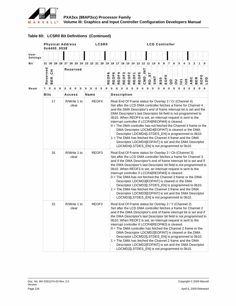
PXA3xx (88AP3xx) Processor FamilyVolume III: Graphics and Input Controller Configuration Developers Manual
Doc. No. MV-S301374-03 Rev. 2.0 Version -
Copyright © 2009 Marvell
Page 126 April 6, 2009 Released
12345678910111213141516171819202122232425262728293031323334353637383940414243444546474849505152535455565758
17 R/Write 1 toclear
REOF4 Real End Of Frame status for Overlay 2 / Cr (Channel 4)Set after the LCD DMA controller fetches a frame for Channel 4 and the DMA Descriptor's end of frame interrupt bit is set and the DMA Descriptor's last Descriptor bit field is not programmed to 0b10. When REOF4 is set, an interrupt request is sent to the interrupt controller if LCCR4[REOFM4] is cleared.0 = The DMA controller has not fetched the Channel 4 frame or the
DMA Descriptor LDCMD4[EOFINT] is cleared or the DMA Descriptor LDCMD4[LSTDES_EN] is programmed to 0b10.
1 = The DMA has fetched the Channel 4 frame and the DMA Descriptor LDCMD4[EOFINT] is set and the DMA Descriptor LDCMD4[LSTDES_EN] is not programmed to 0b10.
16 R/Write 1 toclear
REOF3 Real End Of Frame status for Overlay 2 / Cb (Channel 3)Set after the LCD DMA controller fetches a frame for Channel 3 and if the DMA Descriptor's end of frame interrupt bit is set and if the DMA Descriptor's last Descriptor bit field is not programmed to 0b10. When REOF3 is set, an interrupt request is sent to the interrupt controller if LCCR4[REOFM3] is cleared.0 = The DMA has not fetched the Channel 3 frame or the DMA
Descriptor LDCMD3[EOFINT] is cleared or the DMA Descriptor LDCMD3[LSTDES_EN] is programmed to 0b10.
1 = The DMA has fetched the Channel 3 frame and the DMA Descriptor LDCMD3[EOFINT] is set and the DMA Descriptor LDCMD3[LSTDES_EN] is not programmed to 0b10.
15 R/Write 1 toclear
REOF2 Real End Of Frame status.for Overlay 2 / Y (Channel 2)Set after the LCD DMA controller fetches a frame for Channel 2 and if the DMA Descriptor's end of frame interrupt bit is set and if the DMA Descriptor's last Descriptor bit field is not programmed to 0b10. When REOF2 is set, an interrupt request is sent to the interrupt controller if LCCR4[REOFM2] is cleared.0 = The DMA controller has fetched the Channel 2 frame or the
DMA Descriptor LDCMD2[EOFINT] is cleared or the DMA Descriptor LDCMD2[LSTDES_EN] is programmed to 0b10.
1 = The DMA has fetched the Channel 2 frame and the DMA Descriptor LDCMD2[EOFINT] is set and the DMA Descriptor LDCMD2[LSTDES_EN] is not programmed to 0b10.
Table 60: LCSR0 Bit Definitions (Continued)
Physical Address0x4400_0038
LCSR0 LCD Controller
User Set tings
Bit 31 30 29 28 27 26 25 24 23 22 21 20 19 18 17 16 15 14 13 12 11 10 9 8 7 6 5 4 3 2 1 0
Re
se
rve
d
BE
R_
CH Reserved
RE
OF
6
RE
OF
6
RE
OF
4
RE
OF
3
RE
OF
2
RE
OF
1
RE
OF
0
CM
D_
INT
RD
_S
T
SIN
T
BS
0
EO
F0
QD
OU
IU1
IU0
AB
C
BE
R
SO
F0
LD
D
Reset ? 0 0 0 0 0 0 0 0 0 0 0 0 0 0 0 0 0 0 0 0 0 0 0 0 0 0 0 0 0 0 0
Bits Access Name Description

LCD ControllerLCD Controller Register Descriptions
Copyright © 2009 Marvell Doc. No. MV-S301374-03 Rev. 2.0Version -
April 6, 2009 Released Page 127
12345678910111213141516171819202122232425262728293031323334353637383940414243444546474849505152535455565758
14 R/Write 1 toclear
REOF1 Real End Of Frame status.for Overlay 1 (Channel 1)Set after the LCD DMA controller fetches a frame for Overlay 1 and the DMA Descriptor's end of frame interrupt bit is set and the DMA Descriptor's last Descriptor bit field is not programmed to 0b10. When REOF1 is set, an interrupt request is sent to the interrupt controller if LCCR4[REOFM1] is cleared.0 = The DMA controller has not fetched the Overlay 1 frame or the
DMA Descriptor LDCMD1[EOFINT] is cleared or the DMA Descriptor LDCMD1[LSTDES_EN] is programmed to 0b10.
1 = The DMA has fetched the Overlay 1 frame and the DMA Descriptor LDCMD1[EOFINT] is set and the DMA Descriptor LDCMD1[LSTDES_EN] is not programmed to 0b10.
13 R/Write 1 toclear
REOF0 Real End Of Frame status.for Base (Channel 0)Set after the LCD DMA controller fetches a frame for the base and the DMA Descriptor's end of frame interrupt bit is set and the DMA Descriptor's last Descriptor bit field is not programmed to 0b10. When REOF0 is set, an interrupt request is sent to the interrupt controller if LCCR4[REOFM0] is cleared.0 = The DMA has not fetched the base frame or the DMA
Descriptor LDCMD0[EOFINT] is cleared or the DMA Descriptor LDCMD0[LSTDES_EN] is programmed to 0b10.
1 = The DMA has fetched the base frame and the DMA Descriptor LDCMD0[EOFINT] is set and the DMA Descriptor LDCMD0[LSTDES_EN] is not programmed to 0b10.
12 R/Write 1 toclear
CMD_INT Command Interrupt StatusSet when the LCD controller executes an interrupt command. This bit applies only to panels with an internal frame buffer. When CMD_INT is set, an interrupt is sent to the interrupt controller if it is unmasked (CMDIM=0). CMD_INT remains set until cleared.0 = The LCD controller has not executed the interrupt command.1 = The LCD controller sets this bit when it executes the interrupt
command.
11 R/Write 1 toclear
RD_ST Read StatusSet when the LCD controller executes a Read command to the LCD panel. When RD_ST is set, an interrupt is sent to the interrupt controller if it is unmasked (RDSTM=0). RD_ST remains set until software clears it. 0 = Cleared state of the bit. Software can clear it to zero.1 = The LCD sets this bit when executes the Read command
Table 60: LCSR0 Bit Definitions (Continued)
Physical Address0x4400_0038
LCSR0 LCD Controller
User Set tings
Bit 31 30 29 28 27 26 25 24 23 22 21 20 19 18 17 16 15 14 13 12 11 10 9 8 7 6 5 4 3 2 1 0
Re
se
rve
d
BE
R_
CH Reserved
RE
OF
6
RE
OF
6
RE
OF
4
RE
OF
3
RE
OF
2
RE
OF
1
RE
OF
0
CM
D_
INT
RD
_S
T
SIN
T
BS
0
EO
F0
QD
OU
IU1
IU0
AB
C
BE
R
SO
F0
LD
D
Reset ? 0 0 0 0 0 0 0 0 0 0 0 0 0 0 0 0 0 0 0 0 0 0 0 0 0 0 0 0 0 0 0
Bits Access Name Description

PXA3xx (88AP3xx) Processor FamilyVolume III: Graphics and Input Controller Configuration Developers Manual
Doc. No. MV-S301374-03 Rev. 2.0 Version -
Copyright © 2009 Marvell
Page 128 April 6, 2009 Released
12345678910111213141516171819202122232425262728293031323334353637383940414243444546474849505152535455565758
10 R/Write 1 toclear
SINT Subsequent Interrupt StatusSet when an unmasked interrupt occurs and there is a pending interrupt. The frame ID of the first interrupt is saved in the interrupt frame ID register. This bit is set only for bus error, start of frame, end of frame, branch status, command interrupt, Read status interrupts.
Note: LCD subsequent interrupt is set incorrectly in internal frame buffer mode when a cmd_int_r interrupt status bit occurs.
Software Workaround: When an SINT interrupt occurs, software must read the status registers. If no other interrupts are set (other than the cmd_int interrupt), then this SINT bit is incorrect and no interrupt has occurred.0 = No interrupt.1 = Another interrupt before the previous interrupt (the frame in the
interrupt Frame ID register) is cleared.
9 R/Write 1 toclear
BS0 Branch Status for BaseSet after the DMA controller branches and loads the Descriptor from FBR0[SRCADDR] and the branch interrupt bit (FBR0[BINT]) is set. When the branch status bit is set, an interrupt request is sent to the interrupt controller if the branch status mask is unmasked (LCCR0[BSM0] cleared). BS0 remains set until software clears it. 0 = The DMA has not loaded a branched-to Descriptor, or the DMA
branched but the branch interrupt (FBR0[BINT]) bit is not set. 1 = The DMA has loaded a branched-to Descriptor and the branch
interrupt (FBR0[BINT]) bit is set.
8 R/Write 1 toclear
EOF0 End of Frame Status for Base (Channel 0)Set after the DMA controller fetches a frame from memory and the Channel 0 Descriptor has the end of frame interrupt (EOFINT) bit set (bit 21 of the fourth word of the DMA Descriptor). When EOF0 is set, an interrupt request is made to the interrupt controller if it is unmasked (LCCR0[EOFM0] cleared). EOF0 remains set until cleared by software.0 = A new frame has not been processed or the EOFINT bit is not
set in the fourth word of Channel 0 Descriptor.1 = The DMA has finished fetching a frame and the EOFINT bit is
set in the fourth word of Channel 0 Descriptor.
Table 60: LCSR0 Bit Definitions (Continued)
Physical Address0x4400_0038
LCSR0 LCD Controller
User Set tings
Bit 31 30 29 28 27 26 25 24 23 22 21 20 19 18 17 16 15 14 13 12 11 10 9 8 7 6 5 4 3 2 1 0
Re
se
rve
d
BE
R_
CH Reserved
RE
OF
6
RE
OF
6
RE
OF
4
RE
OF
3
RE
OF
2
RE
OF
1
RE
OF
0
CM
D_
INT
RD
_S
T
SIN
T
BS
0
EO
F0
QD
OU
IU1
IU0
AB
C
BE
R
SO
F0
LD
D
Reset ? 0 0 0 0 0 0 0 0 0 0 0 0 0 0 0 0 0 0 0 0 0 0 0 0 0 0 0 0 0 0 0
Bits Access Name Description

LCD ControllerLCD Controller Register Descriptions
Copyright © 2009 Marvell Doc. No. MV-S301374-03 Rev. 2.0Version -
April 6, 2009 Released Page 129
12345678910111213141516171819202122232425262728293031323334353637383940414243444546474849505152535455565758
7 R/Write 1 toclear
QD LCD Quick Disable StatusSet when LCD enable (ENB) is cleared and the DMA finishes its current data burst. When QD is set, an interrupt request is made to the interrupt controller if it is unmasked (QDM=0). This forces the LCD controller to stop immediately and quit driving the LCD pins. This method of disable is for use with sleep shutdown.0 = LCD has not been quickly disabled by clearing LCD enable
(ENB).1 = LCD has been quickly disabled.
6 R/Write 1 toclear
OU Set when an output FIFO is completely empty and the LCD data pin driver logic attempts to fetch data from the FIFO. When OU is set, an interrupt request is made to the interrupt controller if it is unmasked (OUM=0). 0 = Output FIFO for the lower panel display has not underrun.1 = LCD dither logic not supplying data to output FIFO for the LCD
panel at a sufficient rate. FIFO has completely emptied and data pin driver logic has attempted to take added data from the FIFO.
5 R/Write 1 toclear
IU1 Input FIFO Underrun for Channel 1Set when the input FIFO is completely empty and the LCD pixel unpacking logic attempts to fetch data from the FIFO. When this bit is set, an interrupt request is made to the interrupt controller if it is unmasked (IUM1=0).0 = No underrun.1 = DMA not supplying data to the input FIFO for Channel 1 at a
sufficient rate. FIFO has completely emptied; pixel unpacking logic has attempted to take added data from the FIFO.
4 R/Write 1 toclear
IU0 Input FIFO Underrun for Channel 0Set when the input FIFO is completely empty and the LCD pixel unpacking logic attempts to fetch data from the FIFO. When this bit is set, an interrupt request is made to the interrupt controller if it is unmasked (IUM0=0).0 = No underrun.1 = DMA not supplying data to the input FIFO for Channel 0 at a
sufficient rate. FIFO has completely emptied, pixel unpacking logic has attempted to take added data from the FIFO.
Table 60: LCSR0 Bit Definitions (Continued)
Physical Address0x4400_0038
LCSR0 LCD Controller
User Set tings
Bit 31 30 29 28 27 26 25 24 23 22 21 20 19 18 17 16 15 14 13 12 11 10 9 8 7 6 5 4 3 2 1 0
Re
se
rve
d
BE
R_
CH Reserved
RE
OF
6
RE
OF
6
RE
OF
4
RE
OF
3
RE
OF
2
RE
OF
1
RE
OF
0
CM
D_
INT
RD
_S
T
SIN
T
BS
0
EO
F0
QD
OU
IU1
IU0
AB
C
BE
R
SO
F0
LD
D
Reset ? 0 0 0 0 0 0 0 0 0 0 0 0 0 0 0 0 0 0 0 0 0 0 0 0 0 0 0 0 0 0 0
Bits Access Name Description

PXA3xx (88AP3xx) Processor FamilyVolume III: Graphics and Input Controller Configuration Developers Manual
Doc. No. MV-S301374-03 Rev. 2.0 Version -
Copyright © 2009 Marvell
Page 130 April 6, 2009 Released
12345678910111213141516171819202122232425262728293031323334353637383940414243444546474849505152535455565758
3 R/Write 1 toclear
ABC AC Bias Count StatusSet each time the AC bias pin (L_BIAS) toggles a particular number of times as specified by the AC bias pin transitions per interrupt (API) field in LCCR3. If API is programmed with a non-zero value, a counter is loaded with the value in API and is decremented each time the L_BIAS pin reverses state. When the counter reaches zero, the ABC bit is set, which signals an interrupt request to the interrupt controller. The counter reloads using the value in API, but does not start to decrement again until ABC is cleared by users.0 = AC bias transition counter has not decremented to zero, or API
is programmed to all zeros.1 = AC bias transition counter has decremented to zero, indicating
that the L_BIAS pin has toggled the number of times specified by the API control bit field. Counter is reloaded with the value in API but is disabled until ABC is cleared.
2 R/Write 1 toclear
BER Bus Error StatusSet when a DMA transfer causes a bus error to occur on the system bus. A bus error is signaled when the DMA controller attempts to access a reserved or nonexistent memory space. The bus error channel (BER_CH) specifies for which channel the bus error has occurred. When this occurs, the DMA controller stops and is halted until users program the FDADR register of channel specified by BER_CH with a valid memory address. BER remains set until cleared by software.0 = DMA has not attempted an access to reserved/nonexistent
memory space.1 = DMA has attempted an access to a reserved/nonexistent
location in external memory. The DMA engine stops and must be re-programmed to resume operation.
Table 60: LCSR0 Bit Definitions (Continued)
Physical Address0x4400_0038
LCSR0 LCD Controller
User Set tings
Bit 31 30 29 28 27 26 25 24 23 22 21 20 19 18 17 16 15 14 13 12 11 10 9 8 7 6 5 4 3 2 1 0
Re
se
rve
d
BE
R_
CH Reserved
RE
OF
6
RE
OF
6
RE
OF
4
RE
OF
3
RE
OF
2
RE
OF
1
RE
OF
0
CM
D_
INT
RD
_S
T
SIN
T
BS
0
EO
F0
QD
OU
IU1
IU0
AB
C
BE
R
SO
F0
LD
D
Reset ? 0 0 0 0 0 0 0 0 0 0 0 0 0 0 0 0 0 0 0 0 0 0 0 0 0 0 0 0 0 0 0
Bits Access Name Description

LCD ControllerLCD Controller Register Descriptions
Copyright © 2009 Marvell Doc. No. MV-S301374-03 Rev. 2.0Version -
April 6, 2009 Released Page 131
12345678910111213141516171819202122232425262728293031323334353637383940414243444546474849505152535455565758
1.5.20 LCD Controller Status Register 1 (LCSR1)LCSR1, shown in Table 61, contains interrupt status bits for Overlay 1, Overlay 2, cursor, and command data. Each of these hardware-detected events signals an interrupt request to the interrupt controller. Each LCD status bit signals an interrupt request as long as the bit is set. When the bit is cleared, the interrupt request is cleared. Read/write bits are called status bits (read-only bits are called flags). Status bits are referred to as “sticky” because software must clear them after hardware sets them. Writing a one to a sticky status bit clears it; writing a zero has no effect. Hardware sets and clears read-only flags. Writes have no effect. All LCD interrupts can be masked. See the interrupt controller chapter for details. This is a read/write register. Ignore reads from reserved bits. Write 0b0 to reserved bits.
1 R/Write 1 toclear
SOF0 Start of Frame Status for Base (Channel 0)Set after the DMA controller has loaded a new Descriptor for Channel 0 from memory and that Descriptor has the start of frame interrupt (SOFINT) bit set (bit 22 of the fourth word of the Channel 0 DMA Descriptor). When SOF0 is set, an interrupt request is made to the interrupt controller if it is unmasked (LCCR0[SOFM0] cleared). SOF0 remains set until cleared by software.0 = A new frame Descriptor has not been fetched or the SOFINT
bit is not set in the fourth word of Channel 0 Descriptor.1 = The DMA has begun fetching a new frame and the SOFINT bit
is set in the fourth word of Channel 0 Descriptor.
0 R/Write 1 toclear
LDD LCD Disable Done FlagSet after the LCD has been disabled and the frame that is active finishes being output to the LCD data pins. When the LCD is disabled by setting the LCD disable bit (LCCR0[DIS]), the LCD allows the current frame to complete before it is disabled. After the last set of pixels is clocked out onto the LCD data pins by the pixel clock, the LCD is disabled, LDD is set, and an interrupt request is made to the interrupt controller if it is unmasked (LDM=0). This interrupt is useful to allow an orderly shutdown of the LCD controller before placing the processor into sleep mode.0 = LCD is not disabled and the last active frame completed.1 = LCD is disabled and the last active frame completed.
Table 60: LCSR0 Bit Definitions (Continued)
Physical Address0x4400_0038
LCSR0 LCD Controller
User Set tings
Bit 31 30 29 28 27 26 25 24 23 22 21 20 19 18 17 16 15 14 13 12 11 10 9 8 7 6 5 4 3 2 1 0
Re
se
rve
d
BE
R_
CH Reserved
RE
OF
6
RE
OF
6
RE
OF
4
RE
OF
3
RE
OF
2
RE
OF
1
RE
OF
0
CM
D_
INT
RD
_S
T
SIN
T
BS
0
EO
F0
QD
OU
IU1
IU0
AB
C
BE
R
SO
F0
LD
D
Reset ? 0 0 0 0 0 0 0 0 0 0 0 0 0 0 0 0 0 0 0 0 0 0 0 0 0 0 0 0 0 0 0
Bits Access Name Description

PXA3xx (88AP3xx) Processor FamilyVolume III: Graphics and Input Controller Configuration Developers Manual
Doc. No. MV-S301374-03 Rev. 2.0 Version -
Copyright © 2009 Marvell
Page 132 April 6, 2009 Released
12345678910111213141516171819202122232425262728293031323334353637383940414243444546474849505152535455565758
Table 61: LCSR1 Bit Definitions
Physical Address0x4400_0034
LCSR1 LCD Control ler
User Settings
Bit 31 30 29 28 27 26 25 24 23 22 21 20 19 18 17 16 15 14 13 12 11 10 9 8 7 6 5 4 3 2 1 0
Re
se
rve
d
IU6
IU5
IU4
IU3
IU2
Re
se
rve
d
BS
6
BS
5
BS
4
BS
3
BS
2
BS
1
Re
se
rve
d
EO
F6
EO
F5
EO
F4
EO
F3
EO
F2
EO
F1
Re
se
rve
d
SO
F6
SO
F5
SO
F4
SO
F3
SO
F2
SO
F1
Reset ? ? 0 0 0 0 0 ? ? ? 0 0 0 0 0 0 ? ? 0 0 0 0 0 0 ? ? 0 0 0 0 0 0
Bits Access Name Descript ion
31:30 — — Reserved
29 R/Write 1 toclear
IU6 Input FIFO Underrun for Channel 6 (IU6)Set when the input FIFO is completely empty and the LCD pixel unpacking logic attempts to fetch data from the FIFO. When this bit is set, an interrupt request is made to the interrupt controller if it is unmasked (mask bit LCCR5[IUM6] cleared).0 = No underrun.1 = DMA controller is not supplying data to the input FIFO for
Channel 6 at a sufficient rate. FIFO is empty; pixel unpacking logic has attempted to take added data from the FIFO.
28 R/Write 1 toclear
IU5 Input FIFO Underrun for Channel 5 (IU5)Set when the input FIFO is completely empty and the LCD pixel unpacking logic attempts to fetch data from the FIFO. When this bit is set, an interrupt request is made to the interrupt controller if it is unmasked (mask bit LCCR5[IUM5] cleared).0 = No underrun.1 = DMA controller is not supplying data to the input FIFO for
Channel 5 at a sufficient rate. FIFO is empty; pixel unpacking logic has attempted to take added data from the FIFO.
27 R/Write 1 toclear
IU4 Input FIFO Underrun for Channel 4 (IU4)Set when the input FIFO is empty and the LCD pixel unpacking logic attempts to fetch data from the FIFO. When this bit is set, an interrupt request is sent to the interrupt controller if it is unmasked (mask bit LCCR5[IUM4] cleared).0 = No underrun.1 = DMA is not supplying data to the input FIFO for Channel 4 at a
sufficient rate. FIFO has completely emptied; pixel unpacking logic has attempted to take additional data from the FIFO.
26 R/Write 1 toclear
IU3 Input FIFO Underrun for Channel 3 (IU3)Set when the input FIFO is empty and the LCD pixel unpacking logic attempts to fetch data from the FIFO. When this bit is set, an interrupt request is sent to the interrupt controller if it is unmasked (mask bit LCCR5[IUM3] cleared).0 = No underrun.1 = DMA is not supplying data to the input FIFO for Channel 3 at a
sufficient rate. FIFO has completely emptied; pixel unpacking logic has attempted to take added data from the FIFO.

LCD ControllerLCD Controller Register Descriptions
Copyright © 2009 Marvell Doc. No. MV-S301374-03 Rev. 2.0Version -
April 6, 2009 Released Page 133
12345678910111213141516171819202122232425262728293031323334353637383940414243444546474849505152535455565758
25 R/Write 1 toclear
IU2 Input FIFO Input FIFO for Channel 2 (IU2)Set when the input FIFO is empty and the LCD pixel unpacking logic attempts to fetch data from the FIFO. When this bit is set, an interrupt request is sent to the interrupt controller if it is unmasked (mask bit LCCR5[IUM2] cleared).0 = No underrun.1 = DMA is not supplying data to the input FIFO for Channel 2 at a
sufficient rate. FIFO has completely emptied; pixel unpacking logic has attempted to take added data from the FIFO.
24:22 — — Reserved
21 R/Write 1 toclear
BS6 Branch Status for Channel 6 (Command Register)Set after the DMA controller branches and loads the Descriptor from FBR6[SRCADDR] and the branch interrupt bit (FBR6[BINT]) is set. When BS6 is set, an interrupt request is made to the interrupt controller if the branch status mask is unmasked (LCCR5[BSM6] cleared). BS6 remains set until cleared by software.0 = The DMA controller has not loaded a branched-to Descriptor, or
the DMA branched but the branch interrupt (FBR6[BINT]) bit is not set.
1 = The DMA has loaded a branched-to Descriptor and the branch interrupt (FBR6[BINT]) bit is set.
20 R/Write 1 toclear
BS5 Branch Status for Channel 5 (Hardware Cursor)Set after the DMA controller branches and loads the Descriptor from FBR5[SRCADDR] and the branch interrupt bit (FBR5[BINT]) is set. When BS5 is set, an interrupt request is made to the interrupt controller if the branch status mask is unmasked (LCCR5[BSM5] cleared). BS5 remains set until cleared by software.0 = The DMA controller has not loaded a branched-to Descriptor, or
the DMA branched but the branch interrupt (FBR5[BINT]) bit is not set.
1 = The DMA loaded a branched-to Descriptor and the branch interrupt (FBR5[BINT]) bit is set.
Table 61: LCSR1 Bit Definitions (Continued)
Physical Address0x4400_0034
LCSR1 LCD Control ler
User Settings
Bit 31 30 29 28 27 26 25 24 23 22 21 20 19 18 17 16 15 14 13 12 11 10 9 8 7 6 5 4 3 2 1 0
Re
se
rve
d
IU6
IU5
IU4
IU3
IU2
Re
se
rve
d
BS
6
BS
5
BS
4
BS
3
BS
2
BS
1
Re
se
rve
d
EO
F6
EO
F5
EO
F4
EO
F3
EO
F2
EO
F1
Re
se
rve
d
SO
F6
SO
F5
SO
F4
SO
F3
SO
F2
SO
F1
Reset ? ? 0 0 0 0 0 ? ? ? 0 0 0 0 0 0 ? ? 0 0 0 0 0 0 ? ? 0 0 0 0 0 0
Bits Access Name Descript ion

PXA3xx (88AP3xx) Processor FamilyVolume III: Graphics and Input Controller Configuration Developers Manual
Doc. No. MV-S301374-03 Rev. 2.0 Version -
Copyright © 2009 Marvell
Page 134 April 6, 2009 Released
12345678910111213141516171819202122232425262728293031323334353637383940414243444546474849505152535455565758
19 R/Write 1 toclear
BS4 Branch Status for Channel 4 (Overlay 2)Set after the DMA controller has branched and loaded the Descriptor from FBR4[SRCADDR], and the branch interrupt bit (FBR4[BINT]) is set. When BS4 is set, an interrupt request is made to the interrupt controller if the branch status mask is unmasked (LCCR5[BSM4] cleared). BS6 remains set until software clears it.0 = The DMA controller has not loaded a branched-to Descriptor, or
the DMA branched but the branch interrupt (FBR4[BINT]) bit is not set.
1 = The DMA loaded a branched-to Descriptor and the branch interrupt (FBR4[BINT]) bit is set.
18 R/Write 1 toclear
BS3 Branch Status for Channel 3 (Overlay 2)Set after the DMA controller has branched and loaded the Descriptor from FBR3[SRCADDR], and the branch interrupt bit (FBR3[BINT]) is set. When BS3 is set, an interrupt request is made to the interrupt controller if the branch status mask is unmasked (LCCR5[BSM3] cleared). BS3 remains set until cleared by software.0 = The DMA has not loaded a branched-to Descriptor, or the DMA
branched but the branch interrupt (FBR3[BINT]) bit is not set. 1 = The DMA loaded a branched-to Descriptor and the branch
interrupt (FBR3[BINT]) bit is set.
17 R/Write 1 toclear
BS2 Branch Status for Channel 2 (Overlay 2)Set after the DMA controller branches and loads the Descriptor from FBR2[SRCADDR], and the branch interrupt bit (FBR2[BINT]) is set. When BS2 is set, an interrupt request is sent to the interrupt controller if the branch status mask is unmasked (LCCR5[BSM2] cleared). BS2 remains set until cleared by software.0 = The DMA has not loaded a branched-to Descriptor, or the DMA
branched but the branch interrupt (FBR2[BINT]) bit is not set. 1 = The DMA loaded a branched-to Descriptor and the branch
interrupt (FBR2[BINT]) bit is set.
Table 61: LCSR1 Bit Definitions (Continued)
Physical Address0x4400_0034
LCSR1 LCD Control ler
User Settings
Bit 31 30 29 28 27 26 25 24 23 22 21 20 19 18 17 16 15 14 13 12 11 10 9 8 7 6 5 4 3 2 1 0
Re
se
rve
d
IU6
IU5
IU4
IU3
IU2
Re
se
rve
d
BS
6
BS
5
BS
4
BS
3
BS
2
BS
1
Re
se
rve
d
EO
F6
EO
F5
EO
F4
EO
F3
EO
F2
EO
F1
Re
se
rve
d
SO
F6
SO
F5
SO
F4
SO
F3
SO
F2
SO
F1
Reset ? ? 0 0 0 0 0 ? ? ? 0 0 0 0 0 0 ? ? 0 0 0 0 0 0 ? ? 0 0 0 0 0 0
Bits Access Name Descript ion
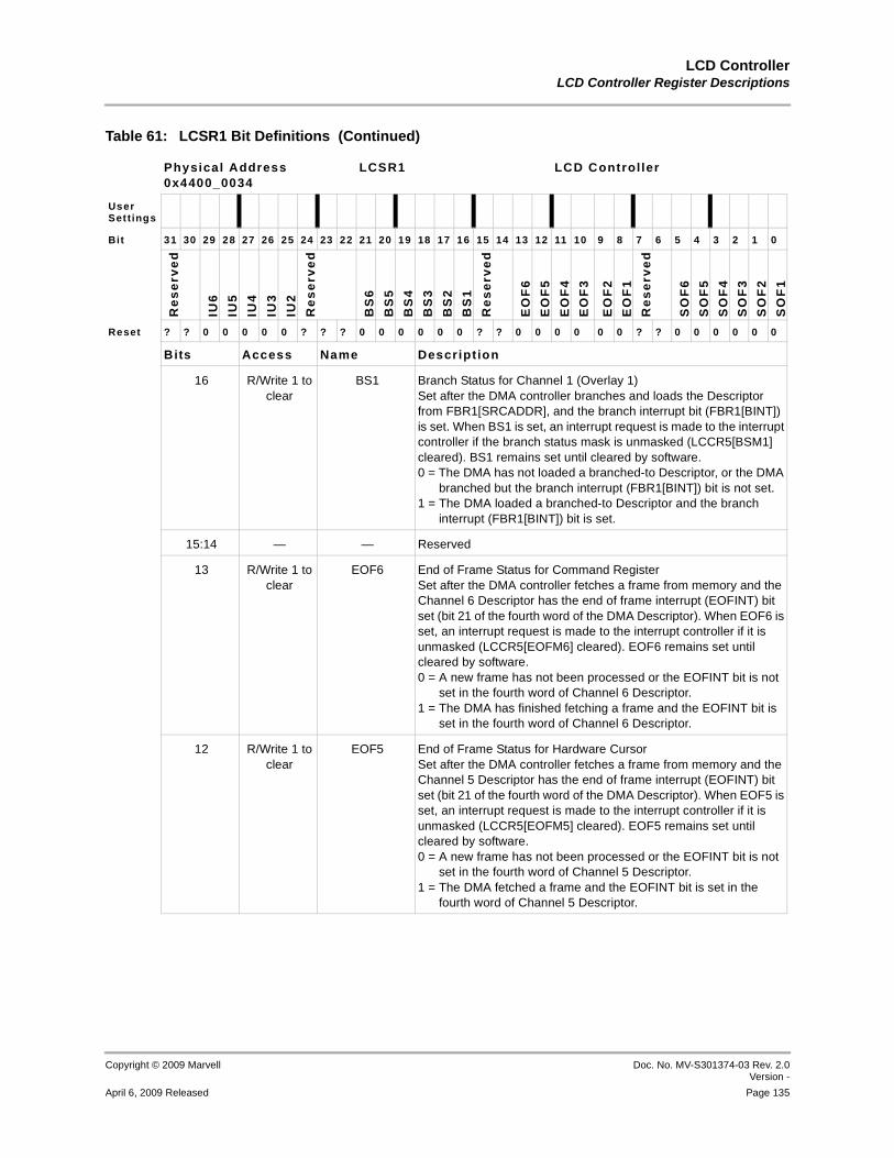
LCD ControllerLCD Controller Register Descriptions
Copyright © 2009 Marvell Doc. No. MV-S301374-03 Rev. 2.0Version -
April 6, 2009 Released Page 135
12345678910111213141516171819202122232425262728293031323334353637383940414243444546474849505152535455565758
16 R/Write 1 toclear
BS1 Branch Status for Channel 1 (Overlay 1)Set after the DMA controller branches and loads the Descriptor from FBR1[SRCADDR], and the branch interrupt bit (FBR1[BINT]) is set. When BS1 is set, an interrupt request is made to the interrupt controller if the branch status mask is unmasked (LCCR5[BSM1] cleared). BS1 remains set until cleared by software.0 = The DMA has not loaded a branched-to Descriptor, or the DMA
branched but the branch interrupt (FBR1[BINT]) bit is not set. 1 = The DMA loaded a branched-to Descriptor and the branch
interrupt (FBR1[BINT]) bit is set.
15:14 — — Reserved
13 R/Write 1 toclear
EOF6 End of Frame Status for Command RegisterSet after the DMA controller fetches a frame from memory and the Channel 6 Descriptor has the end of frame interrupt (EOFINT) bit set (bit 21 of the fourth word of the DMA Descriptor). When EOF6 is set, an interrupt request is made to the interrupt controller if it is unmasked (LCCR5[EOFM6] cleared). EOF6 remains set until cleared by software.0 = A new frame has not been processed or the EOFINT bit is not
set in the fourth word of Channel 6 Descriptor.1 = The DMA has finished fetching a frame and the EOFINT bit is
set in the fourth word of Channel 6 Descriptor.
12 R/Write 1 toclear
EOF5 End of Frame Status for Hardware CursorSet after the DMA controller fetches a frame from memory and the Channel 5 Descriptor has the end of frame interrupt (EOFINT) bit set (bit 21 of the fourth word of the DMA Descriptor). When EOF5 is set, an interrupt request is made to the interrupt controller if it is unmasked (LCCR5[EOFM5] cleared). EOF5 remains set until cleared by software.0 = A new frame has not been processed or the EOFINT bit is not
set in the fourth word of Channel 5 Descriptor.1 = The DMA fetched a frame and the EOFINT bit is set in the
fourth word of Channel 5 Descriptor.
Table 61: LCSR1 Bit Definitions (Continued)
Physical Address0x4400_0034
LCSR1 LCD Control ler
User Settings
Bit 31 30 29 28 27 26 25 24 23 22 21 20 19 18 17 16 15 14 13 12 11 10 9 8 7 6 5 4 3 2 1 0
Re
se
rve
d
IU6
IU5
IU4
IU3
IU2
Re
se
rve
d
BS
6
BS
5
BS
4
BS
3
BS
2
BS
1
Re
se
rve
d
EO
F6
EO
F5
EO
F4
EO
F3
EO
F2
EO
F1
Re
se
rve
d
SO
F6
SO
F5
SO
F4
SO
F3
SO
F2
SO
F1
Reset ? ? 0 0 0 0 0 ? ? ? 0 0 0 0 0 0 ? ? 0 0 0 0 0 0 ? ? 0 0 0 0 0 0
Bits Access Name Descript ion

PXA3xx (88AP3xx) Processor FamilyVolume III: Graphics and Input Controller Configuration Developers Manual
Doc. No. MV-S301374-03 Rev. 2.0 Version -
Copyright © 2009 Marvell
Page 136 April 6, 2009 Released
12345678910111213141516171819202122232425262728293031323334353637383940414243444546474849505152535455565758
11 R/Write 1 toclear
EOF4 End of Frame Status for Overlay 2 (Channel 4)Set after the DMA controller fetches a frame from memory and the Channel 4 Descriptor has the end of frame interrupt (EOFINT) bit set (bit 21 of the fourth word of the DMA Descriptor). When EOF4 is set, an interrupt request is made to the interrupt controller if it is unmasked (LCCR5[EOFM4] cleared). EOF4 remains set until cleared by software.0 = A new frame has not been processed or the EOFINT bit is not
set in the fourth word of Channel 4 Descriptor.1 = The DMA fetched a frame and the EOFINT bit is set in the
fourth word of Channel 4 Descriptor.
10 R/Write 1 toclear
EOF3 End of Frame Status for Overlay 2 (Channel 3)Set after the DMA controller fetches a frame from memory and the Channel 3 Descriptor has the end of frame interrupt (EOFINT) bit set (bit 21 of the fourth word of the DMA Descriptor). When EOF3 is set, an interrupt request is made to the interrupt controller if it is unmasked (LCCR5[EOFM3] cleared). EOF3 remains set until cleared by software.0 = A new frame has not been processed or the EOFINT bit is not
set in the fourth word of Channel 3 Descriptor.1 = The DMA fetched a frame and the EOFINT bit is set in the
fourth word of Channel 3 Descriptor.
9 R/Write 1 toclear
EOF2 End of Frame Status for Overlay 2 (Channel 2)Set after the DMA controller fetches a frame from memory and the Channel 2 Descriptor has the end of frame interrupt (EOFINT) bit set (bit 21 of the fourth word of the DMA Descriptor). When EOF2 is set, an interrupt request is made to the interrupt controller if it is unmasked (LCCR5[EOFM2] cleared). EOF2 remains set until cleared by software.0 = A new frame has not been processed or the EOFINT bit is not
set in the fourth word of Channel 2 Descriptor.1 = The DMA fetched a frame and the EOFINT bit is set in the
fourth word of Channel 2 Descriptor.
Table 61: LCSR1 Bit Definitions (Continued)
Physical Address0x4400_0034
LCSR1 LCD Control ler
User Settings
Bit 31 30 29 28 27 26 25 24 23 22 21 20 19 18 17 16 15 14 13 12 11 10 9 8 7 6 5 4 3 2 1 0
Re
se
rve
d
IU6
IU5
IU4
IU3
IU2
Re
se
rve
d
BS
6
BS
5
BS
4
BS
3
BS
2
BS
1
Re
se
rve
d
EO
F6
EO
F5
EO
F4
EO
F3
EO
F2
EO
F1
Re
se
rve
d
SO
F6
SO
F5
SO
F4
SO
F3
SO
F2
SO
F1
Reset ? ? 0 0 0 0 0 ? ? ? 0 0 0 0 0 0 ? ? 0 0 0 0 0 0 ? ? 0 0 0 0 0 0
Bits Access Name Descript ion

LCD ControllerLCD Controller Register Descriptions
Copyright © 2009 Marvell Doc. No. MV-S301374-03 Rev. 2.0Version -
April 6, 2009 Released Page 137
12345678910111213141516171819202122232425262728293031323334353637383940414243444546474849505152535455565758
8 R/Write 1 toclear
EOF1 End of Frame Status for Channel 1Set after the DMA controller fetches a frame from memory and the Channel 1 Descriptor has the end of frame interrupt (EOFINT) bit set (bit 21 of the fourth word of the DMA Descriptor). When EOF1 is set, an interrupt request is made to the interrupt controller if it is unmasked (LCCR5[EOFM1] cleared). EOF1 remains set until cleared by software.0 = A new frame has not been processed or the EOFINT bit is not
set in the fourth word of Channel 1 Descriptor.1 = The DMA fetched a frame and the EOFINT bit is set in the
fourth word of Channel 1 Descriptor.
7:6 — — Reserved
5 R/Write 1 toclear
SOF6 Start of Frame Status for Command RegisterSet after the DMA controller loads a new Descriptor for Channel 6 from memory and that Descriptor has the start of frame interrupt (SOFINT) bit set (bit 22 of the fourth word of the Channel 6 DMA Descriptor). When SOF6 is set, an interrupt request is made to the interrupt controller if it is unmasked (LCCR5[SOFM6] cleared). SOF6 remains set until software clears it.0 = A new frame Descriptor has not been fetched or the SOFINT bit
is not set in the fourth word of Channel 6 Descriptor.1 = The DMA is fetching a new frame and the SOFINT bit is set in
the fourth word of Channel 6 Descriptor.
4 R/Write 1 toclear
SOF5 Start of Frame Status for Hardware CursorSet after the DMA controller loads a new Descriptor for Channel 5 from memory and that Descriptor has the start of frame interrupt (SOFINT) bit set (bit 22 of the fourth word of the Channel 5 DMA Descriptor). When SOF5 is set, an interrupt request is made to the interrupt controller if it is unmasked (LCCR5[SOFM5] cleared). SOF5 remains set until software clears it.0 = A new frame Descriptor has not been fetched or the SOFINT bit
is not set in the fourth word of Channel 5 Descriptor.1 = The DMA is fetching a new frame and the SOFINT bit is set in
the fourth word of Channel 5 Descriptor.
Table 61: LCSR1 Bit Definitions (Continued)
Physical Address0x4400_0034
LCSR1 LCD Control ler
User Settings
Bit 31 30 29 28 27 26 25 24 23 22 21 20 19 18 17 16 15 14 13 12 11 10 9 8 7 6 5 4 3 2 1 0
Re
se
rve
d
IU6
IU5
IU4
IU3
IU2
Re
se
rve
d
BS
6
BS
5
BS
4
BS
3
BS
2
BS
1
Re
se
rve
d
EO
F6
EO
F5
EO
F4
EO
F3
EO
F2
EO
F1
Re
se
rve
d
SO
F6
SO
F5
SO
F4
SO
F3
SO
F2
SO
F1
Reset ? ? 0 0 0 0 0 ? ? ? 0 0 0 0 0 0 ? ? 0 0 0 0 0 0 ? ? 0 0 0 0 0 0
Bits Access Name Descript ion

PXA3xx (88AP3xx) Processor FamilyVolume III: Graphics and Input Controller Configuration Developers Manual
Doc. No. MV-S301374-03 Rev. 2.0 Version -
Copyright © 2009 Marvell
Page 138 April 6, 2009 Released
12345678910111213141516171819202122232425262728293031323334353637383940414243444546474849505152535455565758
3 R/Write 1 toclear
SOF4 Start of Frame Status for Overlay 2 (Channel 4)Set after the DMA controller loads a new Descriptor for Channel 4 from memory and that Descriptor has the start of frame interrupt (SOFINT) bit set (bit 22 of the fourth word of the Channel 4 DMA Descriptor). When SOF4 is set, an interrupt request is made to the interrupt controller if it is unmasked (LCCR5[SOFM4] cleared). SOF4 remains set until software clears it.0 = A new frame Descriptor has not been fetched or the SOFINT bit
is not set in the fourth word of Channel 4 Descriptor.1 = The DMA is fetching a new frame and the SOFINT bit is set in
the fourth word of Channel 4 Descriptor.
2 R/Write 1 toclear
SOF3 Start of Frame Status for Overlay 2 (Channel 3)Set after the DMA controller loads a new Descriptor for Channel 3 from memory and that Descriptor has the start of frame interrupt (SOFINT) bit set (bit 22 of the fourth word of the Channel 3 DMA Descriptor). When SOF3 is set, an interrupt request is made to the interrupt controller if it is unmasked (LCCR5[SOFM3] cleared). SOF3 remains set until cleared by software.0 = A new frame Descriptor has not been fetched or the SOFINT bit
is not set in the fourth word of Channel 3 Descriptor.1 = The DMA is fetching a new frame and the SOFINT bit is set in
the fourth word of Channel 3 Descriptor.
1 R/Write 1 toclear
SOF2 Start of Frame Status for Overlay 2 (Channel 2)Set after the DMA controller loads a new Descriptor for Channel 2 from memory and that Descriptor has the start of frame interrupt (SOFINT) bit set (bit 22 of the fourth word of the Channel 2 DMA Descriptor). When SOF2 is set, an interrupt request is made to the interrupt controller if it is unmasked (LCCR5[SOFM2] cleared). SOF2 remains set until cleared by software.0 = New frame Descriptor not fetched or the SOFINT bit is not set in
the fourth word of Channel 2 Descriptor.1 = The DMA has begun fetching a new frame and the SOFINT bit
is set in the fourth word of Channel 2 Descriptor.
Table 61: LCSR1 Bit Definitions (Continued)
Physical Address0x4400_0034
LCSR1 LCD Control ler
User Settings
Bit 31 30 29 28 27 26 25 24 23 22 21 20 19 18 17 16 15 14 13 12 11 10 9 8 7 6 5 4 3 2 1 0
Re
se
rve
d
IU6
IU5
IU4
IU3
IU2
Re
se
rve
d
BS
6
BS
5
BS
4
BS
3
BS
2
BS
1
Re
se
rve
d
EO
F6
EO
F5
EO
F4
EO
F3
EO
F2
EO
F1
Re
se
rve
d
SO
F6
SO
F5
SO
F4
SO
F3
SO
F2
SO
F1
Reset ? ? 0 0 0 0 0 ? ? ? 0 0 0 0 0 0 ? ? 0 0 0 0 0 0 ? ? 0 0 0 0 0 0
Bits Access Name Descript ion

LCD ControllerLCD Controller Register Descriptions
Copyright © 2009 Marvell Doc. No. MV-S301374-03 Rev. 2.0Version -
April 6, 2009 Released Page 139
12345678910111213141516171819202122232425262728293031323334353637383940414243444546474849505152535455565758
1.5.21 LCD Controller Interrupt ID Register (LIIDR)LIIDR, shown in Table 62, is a read-only register that contains a copy of the Frame ID register (FIDR) when a start-of- frame (SOF), end-of-frame (EOF), branch (BS), or bus-error (BER) interrupt is signaled. LIIDR is written only when an unmasked interrupt of the above type is signaled and there are no other pending unmasked interrupts in the LCD controller. The register is sticky, and is overwritten only when the signaled interrupt is cleared by writing the LCD Controller Status register.
1.5.22 DMA Frame Source Address Registers (FSADRx)FSADRx, shown in Table 63, contain the source address of the current Descriptor for that channel. The address must be aligned on a 128-bit (16-byte) boundary. This register should point to the memory location at the beginning of the palette data if this Descriptor is a palette load. The size of the palette data should be four entries for 1- and 2-bit pixels, 16 entries for 4-bit pixels, and 256
0 R/Write 1 toclear
SOF1 Start of Frame Status for Overlay 1 (Channel 1)Set after the DMA controller loads a new Descriptor for Channel 1 from memory and that Descriptor has the start of frame interrupt (SOFINT) bit set (bit 22 of the fourth word of the Channel 1 DMA Descriptor). When SOF1 is set, an interrupt request is made to the interrupt controller if it is unmasked (LCCR5[SOFM1] cleared). SOF1 remains set until cleared by software.0 = New frame Descriptor not fetched or the SOFINT bit is not set in
the fourth word of Channel 1 Descriptor.1 = The DMA is fetching a new frame and the SOFINT bit is set in
the fourth word of Channel 1 Descriptor.
Table 61: LCSR1 Bit Definitions (Continued)
Physical Address0x4400_0034
LCSR1 LCD Control ler
User Settings
Bit 31 30 29 28 27 26 25 24 23 22 21 20 19 18 17 16 15 14 13 12 11 10 9 8 7 6 5 4 3 2 1 0
Re
se
rve
d
IU6
IU5
IU4
IU3
IU2
Re
se
rve
d
BS
6
BS
5
BS
4
BS
3
BS
2
BS
1
Re
se
rve
d
EO
F6
EO
F5
EO
F4
EO
F3
EO
F2
EO
F1
Re
se
rve
d
SO
F6
SO
F5
SO
F4
SO
F3
SO
F2
SO
F1
Reset ? ? 0 0 0 0 0 ? ? ? 0 0 0 0 0 0 ? ? 0 0 0 0 0 0 ? ? 0 0 0 0 0 0
Bits Access Name Descript ion
Table 62: LIIDR Bit Definitions
Physical Address0x4400_003C
LIIDR LCD Controller
User Settings
Bit 31 30 29 28 27 26 25 24 23 22 21 20 19 18 17 16 15 14 13 12 11 10 9 8 7 6 5 4 3 2 1 0
IFRAMEID
Reset ? ? ? ? ? ? ? ? ? ? ? ? ? ? ? ? ? ? ? ? ? ? ? ? ? ? ? ? ? ? ? ?
Bits Access Name Descript ion
31:0 R IFRAMEID Interrupt Frame ID

PXA3xx (88AP3xx) Processor FamilyVolume III: Graphics and Input Controller Configuration Developers Manual
Doc. No. MV-S301374-03 Rev. 2.0 Version -
Copyright © 2009 Marvell
Page 140 April 6, 2009 Released
12345678910111213141516171819202122232425262728293031323334353637383940414243444546474849505152535455565758
entries for 8-bit pixels. This register should point to the beginning of the frame data in memory if this Descriptor is for pixel data. This address is incremented as the DMA controller fetches from memory. If preferred, the DMA Frame ID register can be used to hold the initial frame source address. See Table 63. This is a read/write register. Ignore reads from reserved bits. Write 0b0 to reserved bits.
1.5.23 DMA Frame ID Registers (FIDRx)FIDRx contains a 32-bit ID field to describe the current frame. The particular use of this field remains with users. This ID register is copied to the LCD Controller Interrupt ID register when an interrupt occurs. See Table 64. This is a read-only register. Ignore reads from reserved bits.
Table 63: FSADR0/1/2/3/4/5/6 Bit Definitions
Physical Address0x4400_02040x4400_02140x4400_02240x4400_02340x4400_02440x4400_02540x4400_0264
FSADR0FSADR1FSADR2FSADR3FSADR4FSADR5FSADR6
LCD Control ler
User Settings
Bit 31 30 29 28 27 26 25 24 23 22 21 20 19 18 17 16 15 14 13 12 11 10 9 8 7 6 5 4 3 2 1 0
SRCADDR 0 0 0 0 0
Reset 0 0 0 0 0 0 0 0 0 0 0 0 0 0 0 0 0 0 0 0 0 0 0 0 0 0 0 0 ? ? ? ?
Bits Access Name Description
31:5 R/W SRCADDR Frame Source AddressAddress of the palette or pixel frame data in memory.
4:0 — — Must be zeros.
Table 64: FIDR0/1/2/3/4/5/6 Bit Definitions
Physical Address0x4400_02080x4400_02180x4400_02280x4400_02380x4400_02480x4400_02580x4400_0268
FIDR0FIDR1FIDR2FIDR3FIDR4FIDR5FIDR6
LCD Control ler
User Set tings
Bit 31
30
29
28
27
26
25
24
23
22
21
20
19
18
17
16
15
14
13
12
11
10
9 8 7 6 5 4 3 2 1 0
FRAME ID Reserved
Reset 0 0 0 0 0 0 0 0 0 0 0 0 0 0 0 0 0 0 0 0 0 0 0 0 0 0 0 0 0 0 0 ?
Bits Access Name Descript ion
31:3 R FRAME ID Frame ID

LCD ControllerLCD Controller Register Descriptions
Copyright © 2009 Marvell Doc. No. MV-S301374-03 Rev. 2.0Version -
April 6, 2009 Released Page 141
12345678910111213141516171819202122232425262728293031323334353637383940414243444546474849505152535455565758
1.5.24 LCD DMA Command Register (LDCMDx)LDCMDx, shown in Table 65, contain the command and length of the current Descriptor for that channel. The bits in this register are initialized to zero on powerup. This is a read-only register. Ignore reads from reserved bits.
2:0 — — Reserved
Table 64: FIDR0/1/2/3/4/5/6 Bit Definitions (Continued)
Physical Address0x4400_02080x4400_02180x4400_02280x4400_02380x4400_02480x4400_02580x4400_0268
FIDR0FIDR1FIDR2FIDR3FIDR4FIDR5FIDR6
LCD Control ler
User Set tings
Bit 31
30
29
28
27
26
25
24
23
22
21
20
19
18
17
16
15
14
13
12
11
10
9 8 7 6 5 4 3 2 1 0
FRAME ID Reserved
Reset 0 0 0 0 0 0 0 0 0 0 0 0 0 0 0 0 0 0 0 0 0 0 0 0 0 0 0 0 0 0 0 ?
Bits Access Name Descript ion
Table 65: LDCMD0/1/2/3/4/5/6 Bit Definitions
Physical Address0x4400_020C0x4400_021C0x4400_022C0x4400_023C0x4400_024C0x4400_025C0x4400_026C
LDCMD0LDCMD1LDCMD2LDCMD3LDCMD4LDCMD5LDCMD6
LCD Controller
User Set tings
Bit 31 30 29 28 27 26 25 24 23 22 21 20 19 18 17 16 15 14 13 12 11 10 9 8 7 6 5 4 3 2 1 0
Reserved
PA
L
Re
se
rve
d
LS
TD
ES
_E
N
SO
FIN
T
EO
FIN
T
LENGTH
Re
se
rve
d
Reset ? ? ? ? ? 0 ? 0 0 0 0 0 0 0 0 0 0 0 0 0 0 0 0 0 0 0 0 0 0 0 ? ?
Bits Access Name Description
31:27 — — Reserved

PXA3xx (88AP3xx) Processor FamilyVolume III: Graphics and Input Controller Configuration Developers Manual
Doc. No. MV-S301374-03 Rev. 2.0 Version -
Copyright © 2009 Marvell
Page 142 April 6, 2009 Released
12345678910111213141516171819202122232425262728293031323334353637383940414243444546474849505152535455565758
26 R PAL Palette BufferIf set, indicates to the DMA controller that the data being fetched is the palette buffer and it must be loaded into the palette RAM. The palette RAM must be loaded at least once before using the LCD controller (unless more then 8-bit pixels are used). The size of the palette is 256 entries of palette data0 = Data in DMA Descriptor is the frame buffer data.1 = Data in DMA Descriptor is the palette buffer data and is to be
loaded into the palette RAM
25 — — Reserved
Table 65: LDCMD0/1/2/3/4/5/6 Bit Definitions (Continued)
Physical Address0x4400_020C0x4400_021C0x4400_022C0x4400_023C0x4400_024C0x4400_025C0x4400_026C
LDCMD0LDCMD1LDCMD2LDCMD3LDCMD4LDCMD5LDCMD6
LCD Controller
User Set tings
Bit 31 30 29 28 27 26 25 24 23 22 21 20 19 18 17 16 15 14 13 12 11 10 9 8 7 6 5 4 3 2 1 0
Reserved
PA
L
Re
se
rve
d
LS
TD
ES
_E
N
SO
FIN
T
EO
FIN
TLENGTH
Re
se
rve
d
Reset ? ? ? ? ? 0 ? 0 0 0 0 0 0 0 0 0 0 0 0 0 0 0 0 0 0 0 0 0 0 0 ? ?
Bits Access Name Description

LCD ControllerLCD Controller Register Descriptions
Copyright © 2009 Marvell Doc. No. MV-S301374-03 Rev. 2.0Version -
April 6, 2009 Released Page 143
12345678910111213141516171819202122232425262728293031323334353637383940414243444546474849505152535455565758
24:23 R LSTDES_EN Last Descriptor When multiple Descriptors are used, LSTDES_EN configures the behavior of LCSR0[REOFx] upon completion of the Descriptor. Program this bit field with 0b00 or 0b01 when only one Descriptor is used for each frame data and with 0b10 or 0b11 when more than one Descriptor is used for the frame data. The bit fields configure the following behavior:• 0b11 = Last Descriptor of the frame buffer. Set LCSR0[REOFx]
and LCSR1[EOFx] (LCSR0[EOF0] if Channel 0) after completion of this Descriptor. Take the branch if FBRx[BINT] is set.
• 0b10 = Not the last Descriptor of the frame buffer. Only set LCSR1[EOFx] (LCSR0[EOF0] if Channel 0) after completion of this Descriptor. Do not branch even if FBRx[BINT] is set.
• 0b01 or 0b00 = Set LCSR0[REOFx] and LCSR1[EOFx] (LCSR0[EOF0] if Channel 0) after completion of this Descriptor. Take the branch if FBRx[BINT] is set.
• The palette data must have only one Descriptor. Also cursor does not support multiple Descriptors. So cursor must have only one Descriptor.
• The intermediate Descriptors when multiple Descriptors are used should be 128 bit aligned.
Note: Normal disable does not work in multi-Descriptor mode. To disable the LCD controller when multiple Descriptors are used, do one of the following:• Do quick disable instead of normal disable.• Write to the Branch register to branch to a single Descriptor
and wait for a branch interrupt. Then do a normal disable.
Table 65: LDCMD0/1/2/3/4/5/6 Bit Definitions (Continued)
Physical Address0x4400_020C0x4400_021C0x4400_022C0x4400_023C0x4400_024C0x4400_025C0x4400_026C
LDCMD0LDCMD1LDCMD2LDCMD3LDCMD4LDCMD5LDCMD6
LCD Controller
User Set tings
Bit 31 30 29 28 27 26 25 24 23 22 21 20 19 18 17 16 15 14 13 12 11 10 9 8 7 6 5 4 3 2 1 0
Reserved
PA
L
Re
se
rve
d
LS
TD
ES
_E
N
SO
FIN
T
EO
FIN
TLENGTH
Re
se
rve
d
Reset ? ? ? ? ? 0 ? 0 0 0 0 0 0 0 0 0 0 0 0 0 0 0 0 0 0 0 0 0 0 0 ? ?
Bits Access Name Description

PXA3xx (88AP3xx) Processor FamilyVolume III: Graphics and Input Controller Configuration Developers Manual
Doc. No. MV-S301374-03 Rev. 2.0 Version -
Copyright © 2009 Marvell
Page 144 April 6, 2009 Released
12345678910111213141516171819202122232425262728293031323334353637383940414243444546474849505152535455565758
22 R SOFINT Start of Frame Interrupt When set, the DMA controller sets the corresponding start-of- frame bit (LCSR1[SOFx]) when starting a new frame. The bit is set after a new Descriptor is loaded from memory and before the palette/frame data is fetched.1 = Set the start of frame (SOF) interrupt request bit in the LCD
Status register when starting a new frame (after loading the frame Descriptor).
0 = Do not set SOF.
21 R EOFINT End of the Frame Interrupt Mask When set, the DMA controller sets the corresponding end-of- frame bit (LCSR1[EOFx]) after fetching the last word in the frame buffer, that is, when the DMA length counter decrements to zero.1 = Set the end of frame (EOF) interrupt request bit in the LCD
status register after the last word of this frame is fetched.0 = Do not set EOF.
20:2 R LENGTH Length of Transfer in Bytes Determines how many bytes of data the DMA controller fetches. Clearing LENGTH is invalid. If PAL is set, LENGTH must be programmed with the size of the palette RAM. This corresponds to 512 or 1024 bytes for 8-bit pixels. A separate Descriptor must be used to fetch the frame data. The value of LENGTH for frame data is a function of the screen size and the pixel size. The transfer length must be word (32-bit) aligned. For Overlay 2 data that is in 4:2:2 or 4:2:0 YCbCr formats, the frame length may not naturally align to a 32-bit boundary. The transfer length must be programmed to the next 32-bit word and padded with dummy pixels at the end of the frame (which the LCD controller ignores). The two lowest bits [1:0] must always be zero for proper alignment. Writes to these two lower bits are ignored.
1:0 — — Reserved
Table 65: LDCMD0/1/2/3/4/5/6 Bit Definitions (Continued)
Physical Address0x4400_020C0x4400_021C0x4400_022C0x4400_023C0x4400_024C0x4400_025C0x4400_026C
LDCMD0LDCMD1LDCMD2LDCMD3LDCMD4LDCMD5LDCMD6
LCD Controller
User Set tings
Bit 31 30 29 28 27 26 25 24 23 22 21 20 19 18 17 16 15 14 13 12 11 10 9 8 7 6 5 4 3 2 1 0
Reserved
PA
L
Re
se
rve
d
LS
TD
ES
_E
N
SO
FIN
T
EO
FIN
TLENGTH
Re
se
rve
d
Reset ? ? ? ? ? 0 ? 0 0 0 0 0 0 0 0 0 0 0 0 0 0 0 0 0 0 0 0 0 0 0 ? ?
Bits Access Name Description
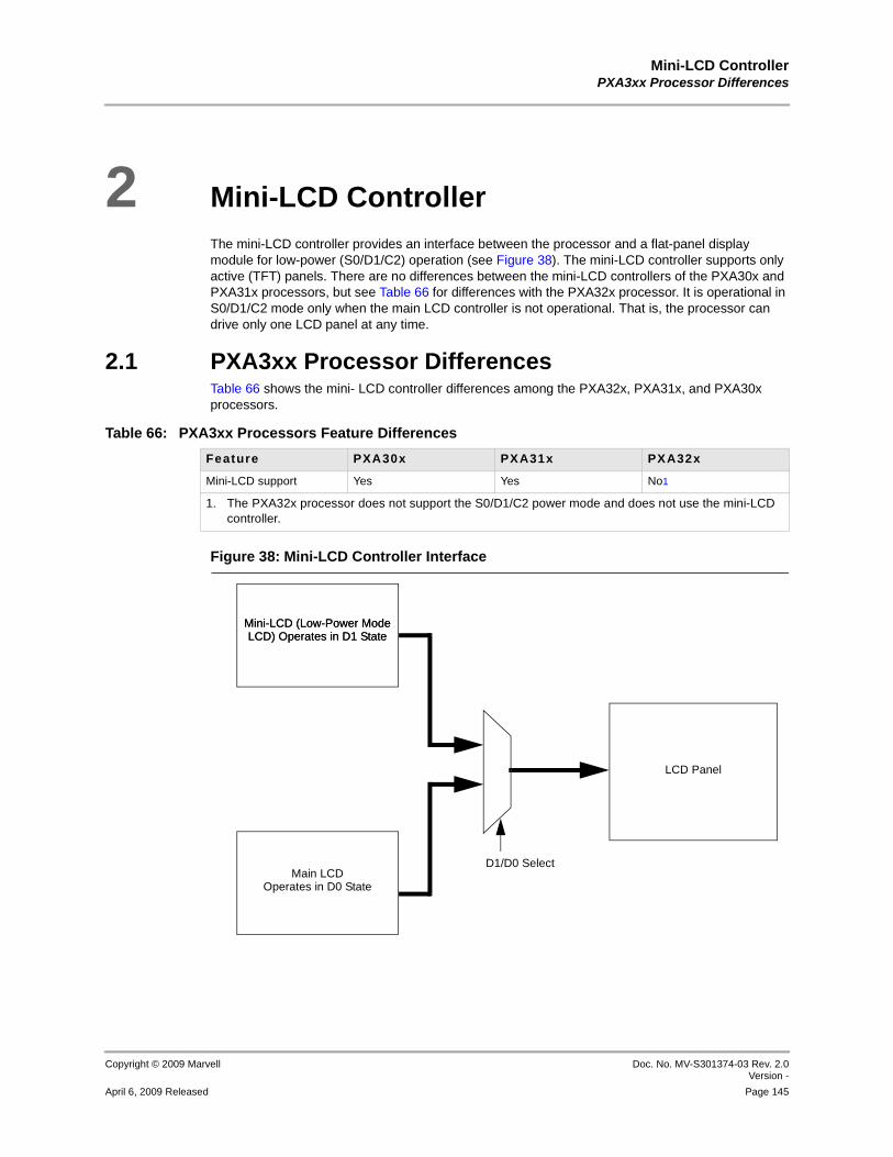
Mini-LCD ControllerPXA3xx Processor Differences
Copyright © 2009 Marvell Doc. No. MV-S301374-03 Rev. 2.0Version -
April 6, 2009 Released Page 145
12345678910111213141516171819202122232425262728293031323334353637383940414243444546474849505152535455565758
2 Mini-LCD ControllerThe mini-LCD controller provides an interface between the processor and a flat-panel display module for low-power (S0/D1/C2) operation (see Figure 38). The mini-LCD controller supports only active (TFT) panels. There are no differences between the mini-LCD controllers of the PXA30x and PXA31x processors, but see Table 66 for differences with the PXA32x processor. It is operational in S0/D1/C2 mode only when the main LCD controller is not operational. That is, the processor can drive only one LCD panel at any time.
2.1 PXA3xx Processor DifferencesTable 66 shows the mini- LCD controller differences among the PXA32x, PXA31x, and PXA30x processors.
Figure 38: Mini-LCD Controller Interface
Table 66: PXA3xx Processors Feature Differences
Feature PXA30x PXA31x PXA32x
Mini-LCD support Yes Yes No1
1. The PXA32x processor does not support the S0/D1/C2 power mode and does not use the mini-LCD controller.
LCD Panel
D1/D0 Select
Mini-LCD (Low-Power ModeLCD) Operates in D1 State
Main LCDOperates in D0 State
Mini-LCD (Low-Power ModeLCD) Operates in D1 State

PXA3xx (88AP3xx) Processor FamilyVolume III: Graphics and Input Controller Configuration Developers Manual
Doc. No. MV-S301374-03 Rev. 2.0 Version -
Copyright © 2009 Marvell
Page 146 April 6, 2009 Released
12345678910111213141516171819202122232425262728293031323334353637383940414243444546474849505152535455565758
2.2 FeaturesThe mini-LCD is used in low-power operating mode (S0/D1/C2) when the main LCD controller is disabled. The mini-LCD controller offers a subset of the main LCD controller features. It does not have overlays or cursor but does have the following features:
Display mode
• Active color mode for up to 32768 colors (15 bits)
• Output formats of 16-bit or 18-bit display. See the GPIO and Pins and Control chapter in PXA3xx Processor Family Vol. I: System and Timer Configuration Developers Manual for information on how to set up the GPIO signals for the 18-bit display.
RGB 1:5:5:5 input pixel format only. See Section 2.4.1 for details.The following display sizes (both portrait and landscape formats).
• 176 × 208
• 176 × 220
• 240 × 240
• 320 × 240 (QVGA)
• 320 × 320
• 320 × 480
• 480 × 480
• 640 × 480 (VGA)
• 800 × 600
Programmable horizontal blanking at the beginning and end of each line and vertical blanking for the frameProgrammable polarity for output enable, frame clock, and line clock
Operates at 39 MHz frequency
2.3 SignalsWhen the Mini-LCD controller is disabled, all of its pins can be used for general-purpose input/output (GPIO) or other functions according to the multi-function pin assignment. Refer to the GPIO chapter in Volume I of the Developer’s Manual.
Table 67: Mini-LCD Interface Signals
Pin Name Type Definit ion
ML_DD<17:0> Output Data lines to transmit 16/18-bit data values at a time to the LCD display module.
ML_PCLK Output Pixel clock used by the LCD display module to clock the pixel data into the line shift register. The pixel clock transitions continuously, and the ML_EN_BIAS pin is used as an output to signal when data is valid on the mini-LCD data pins.
ML_LCLK Output Line clock used by the LCD display module to signal the end of a line of pixels that transfers the line data from the shift register to the screen and to increment the line pointers.
ML_FCLK Output Frame clock used by the LCD display module to signal the start of a new frame of pixels that resets the line pointers to the top of the screen.
ML_EN_BIAS Output Enable signal used as the output-enable to signal when data is latched from the data pins using the pixel clock.

Mini-LCD ControllerOperation
Copyright © 2009 Marvell Doc. No. MV-S301374-03 Rev. 2.0Version -
April 6, 2009 Released Page 147
12345678910111213141516171819202122232425262728293031323334353637383940414243444546474849505152535455565758
2.4 OperationThe mini-LCD controller displays the data in S0/D1/C2 when the main LCD controller is turned off. It gets the frame data from the internal SRAM memory through a private interface. The outputs of the mini-LCD controller are multiplexed with those of the main LCD controller before they are sent out of the processor on the multi-function pins. The mini-LCD controller provides user-programmable options for display resolution and frame counts to assert wakeup events. Although all programmable combinations are possible, the selection of displays available within the market dictates which combinations of these programmable options are practical. The display sizes are summarized in the features section at the beginning of this chapter.
2.4.1 Input Pixel FormatsThe mini-LCD controller supports 16-bit RGB 1:5:5:5 format. The MSB bit of the pixel value is called the count value enable. If the count value enable bit (bit 15) of the pixel is 0, the lower 15 bits represent the RGB 5:5:5 color value as illustrated in Table 68. If the count value enable (bit 15) is 1, the lower 15 bits do not contain color information but instead contain information for repeating the previous pixel color or controlling the frame/line timing. The format of the pixel when the count value pixel is set is described in Table 69.
If the MSB bit is equal to 1, the lower 12 bits [11:0] represent the count value to repeat the last color. Bits [14:12] indicate whether the pixel is the last pixel of the line, the last pixel of the frame, not a valid pixel, or otherwise. The count value should be greater than or equal to 1.
The last pixel of each line must be of this format with count value equal to 1. Therefore, the last two pixels of each line must be identical in the unencoded frame. If bits [14:12] = 0b001, the pixel is the last pixel of the line. If bits [14:12] = 0b010, the pixel is the last pixel of the frame. If the bits [14:12] = 0b111, the pixel is not valid and are used to pad the frame data when the frame length is not multiple of 64 bits. See Table 70. The mini-LCD displays all zeros if the first pixel value is the count value.
Table 68: RGB 5:5:5 Pixel Format, Count Value Enable Bit Cleared
15 14 10 9 5 4 0
0 Red [4:0] Green [4:0] Blue [4:0]
Table 69: Pixel Format - Count Value Enable Bit Set
15 14 12 11 0
1 EOL/EOF Count Value
Table 70: Pixel Value with Count Value Enable Bit Set to 1
Count Value Enable
EOL/EOF Count Value
Comments
1 001 1 The pixel is the last pixel of the line. The last pixel of each line except for the last line of the frame should have this format.
1 010 1 The pixel is the last pixel of the frame. The last pixel of the frame should have this format.

PXA3xx (88AP3xx) Processor FamilyVolume III: Graphics and Input Controller Configuration Developers Manual
Doc. No. MV-S301374-03 Rev. 2.0 Version -
Copyright © 2009 Marvell
Page 148 April 6, 2009 Released
12345678910111213141516171819202122232425262728293031323334353637383940414243444546474849505152535455565758
The pixel data must be stored in the internal SRAM. The amount of the pixel data depends on the size of the screen or compression. This compression technique is used so that you can fit a big frame data into less SRAM memory. It also reduces the bandwidth from the SRAM to the mini-LCD controller. All of the run-length encoding (RLE) data must fit into the internal SRAM memory. The size of the memory depends on the image displayed or compression of the pixel data. The pixel entries are ordered starting with the least significant bit and ending with the most significant bit in a 32-bit word. The frame data must start on 64-bit address boundary. Table 71 shows the format in which the pixel data is stored in internal memory.
2.4.2 Mini-LCD Output InterfaceThe output data bus is 16 bits wide. The 15-bit pixel data is driven onto the 16-bit output bus. The 15-bit pixel data is expanded to 16-bit output data by duplicating the GREEN[0] bit as shown in Table 72.
2.4.3 Power Manager InterfaceWhen the Mini-LCD Frame Count Register (MLFRMCNT) WKUP_EN bit is set (see Table 78, “MLFRMCNT Bit Definitions,” on page 157), the mini-LCD asserts a wakeup event to exit S0/D1/C2 mode and enter S0/D0/C0 mode after displaying the number of frames equal to the value programmed in MLFRMCNT[FRCOUNT]. FRCOUNT is decremented by one after each frame is displayed. The S0/D1/C2-to-S0/D0/C0 wakeup event occurs when FRCOUNT is decremented to zero. The power manager exits the S0/D1/C2 mode and asserts the clear signal for the wakeup interrupt to be cleared. Because MLFRMCNT is reset when the processor exits S0/D1/C2 mode, this register must be re-programmed before re-entering S0/D1/C2 mode from S0/D0/C0 mode.
When MLFRMCNT[FWKUP_EN] is set, the mini-LCD asserts a wakeup event to exit S0/D1/C2 mode and enter S0/D2/C2 mode after displaying each frame. MLFRMCNT[FWKUP_EN] is not affected by FRCOUNT.
1 111 NA Invalid pixel. It is ignored.
1 Others Count Value Repeat the last color.
Table 71: Memory Organization for Pixel Data
Memory Organization
31 16 15 0
Pixel 1 Pixel 0
Pixel 3 Pixel 2
Table 70: Pixel Value with Count Value Enable Bit Set to 1 (Continued)
Count Value Enable
EOL/EOF Count Value
Comments
Table 72: Output Data Bus
15 11 10 5 4 0
Red [4:0] Green [4:0], Green[0] Blue [4:0]

Mini-LCD ControllerOperation
Copyright © 2009 Marvell Doc. No. MV-S301374-03 Rev. 2.0Version -
April 6, 2009 Released Page 149
12345678910111213141516171819202122232425262728293031323334353637383940414243444546474849505152535455565758
2.4.4 Mini-LCD Input FIFOThe mini-LCD controller contains an 8-entry × 16-bit-wide input FIFO to store pixel data read from the internal SRAM before it is driven out to the output LCD pins. When four FIFO entries are empty, the mini-LCD requests the next 64 bits of data to the internal memory controller. The pixels are read from the bottom of the FIFO and are driven out to the pins.
2.4.5 Functional TimingThe pixel-clock frequency must be adjusted to meet the required screen-refresh rate, which depends on several factors:
Number of pixels for the target displayNumber of pixel clock wait states programmed at the beginning and end of each line
Number of line clocks inserted at the beginning and end of each frame Width of the frame clock
All of these factors alter the interval from one frame transmission to the next. Different display manufacturers require different frame-refresh rates, depending on the physical characteristics of the display. MLCCR0[PCD] is used to alter the pixel clock frequency to meet these requirements. The frequency of the pixel clock for a set PCD value or the required PCD value to yield a target pixel clock frequency can be calculated using the two following equations.
Figure 39 illustrates the output pin timing. The value of MLCCR0[VSP], MLCCR0[HSP], and MLCCR0[PCP] define the polarity of the frame clock, line clock, and pixel clock, respectively.
Figure 40 illustrates the output data pin timing with respect to the pixel clock.
PixelClock CLKMLCDPCD 1+( )
------------------------------=
PCD CLKMLCDPixelClock( )
------------------------------------ 1–=

PXA3xx (88AP3xx) Processor FamilyVolume III: Graphics and Input Controller Configuration Developers Manual
Doc. No. MV-S301374-03 Rev. 2.0 Version -
Copyright © 2009 Marvell
Page 150 April 6, 2009 Released
12345678910111213141516171819202122232425262728293031323334353637383940414243444546474849505152535455565758
2.5 Register DescriptionsThe mini-LCD controller contains three control registers, one SRAM Address register, and a Frame Counter register. Write to the mini-LCD control registers to program the following:
Height and width of the displayPolarity of the control signals
Figure 39: Mini-LCD Controller Pin Timing Diagram
Line 0 Data Line 1 Data Line 2 Data
PPL = 31
ELW = 0 BLW = 0
HSW = 1 VSW = 1
VSP = MLCCR0[VSP]. The Frame Clock Polarity
ML_FCLK
ML_LCLK
ML_PCLK
ML_DD<15:0>
PCP = 1
VSP = 0
HSP = 0
HSP = MLCCR0[HSP]. The Line Clock Polarity
PCP = MLCCR0[PSP]. The Pixel Clock Polarity
VSW is the Vertical Sync (Frame Clock) Pulse Width = MLCCR2[VSW] – 1
HSW is the Horizontal Sync (Line Clock) Pulse Width = MLCCR1[HSW] – 1
BLW is the Beginning-of-Line Pixel Clock Wait Count = MLCCR2[BLW] – 1
ELW is the End-of-Line Pixel Clock Wait Count = MLCCR1[ELW] – 1
Figure 40: Active Mode Pixel Clock and Data Pin Timing
Pixel 0 Pixel 1 Pixel 2 Pixel 3 Pixel 4
PCP - Pixel Clock Polarity
0 = Pixels sampled from data pins on rising edge of clock
1 = Pixels sampled from data pins on falling edge of clock
ML_BIAS
ML_PCLK
ML_DD[15:0]
PCP = 0
For PCP = 0 and for PCP = 1 data is driven out at the same time; ML_PCLK is simply inverted for PCP=1.
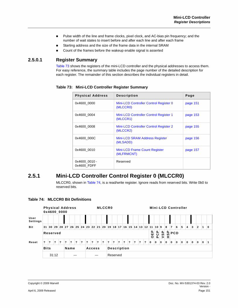
Mini-LCD ControllerRegister Descriptions
Copyright © 2009 Marvell Doc. No. MV-S301374-03 Rev. 2.0Version -
April 6, 2009 Released Page 151
12345678910111213141516171819202122232425262728293031323334353637383940414243444546474849505152535455565758
Pulse width of the line and frame clocks, pixel clock, and AC-bias pin frequency; and the number of wait states to insert before and after each line and after each frameStarting address and the size of the frame data in the internal SRAMCount of the frames before the wakeup enable signal is asserted
2.5.0.1 Register SummaryTable 73 shows the registers of the mini-LCD controller and the physical addresses to access them. For easy reference, the summary table includes the page number of the detailed description for each register. The remainder of this section describes the individual registers in detail.
2.5.1 Mini-LCD Controller Control Register 0 (MLCCR0)MLCCR0, shown in Table 74, is a read/write register. Ignore reads from reserved bits. Write 0b0 to reserved bits.
Table 73: Mini-LCD Controller Register Summary
Physical Address Description Page
0x4600_0000 Mini-LCD Controller Control Register 0 (MLCCR0)
page 151
0x4600_0004 Mini-LCD Controller Control Register 1 (MLCCR1)
page 153
0x4600_0008 Mini-LCD Controller Control Register 2 (MLCCR2)
page 155
0x4600_000C Mini-LCD SRAM Address Register (MLSADD)
page 156
0x4600_0010 Mini-LCD Frame Count Register (MLFRMCNT)
page 157
0x4600_0010 - 0x4600_FDFF
Reserved
Table 74: MLCCR0 Bit Definitions
Physical Address0x4600_0000
MLCCR0 Mini-LCD Control ler
User Settings
Bit 31 30 29 28 27 26 25 24 23 22 21 20 19 18 17 16 15 14 13 12 11 10 9 8 7 6 5 4 3 2 1 0
Reserved
OE
P
PC
P
VS
P
HS
P PCD
Reset ? ? ? ? ? ? ? ? ? ? ? ? ? ? ? ? ? ? ? ? 0 0 0 0 0 0 0 0 0 0 0 1
Bits Name Access Description
31:12 — — Reserved

PXA3xx (88AP3xx) Processor FamilyVolume III: Graphics and Input Controller Configuration Developers Manual
Doc. No. MV-S301374-03 Rev. 2.0 Version -
Copyright © 2009 Marvell
Page 152 April 6, 2009 Released
12345678910111213141516171819202122232425262728293031323334353637383940414243444546474849505152535455565758
11 OEP R/W Output Enable PolaritySelects the active and inactive states of the output enable signal in active display mode. The AC bias pin is used as an enable that signals the external device when data is actively being driven out using the pixel clock. The pixel clock continuously toggles during operation. Data is driven onto the LCD data pins on the programmed edge of the ML_PCLK pin when L_BIAS is in its active state. 0 = ML_BIAS pin is active high and inactive low.1 = ML_BIAS pin is active low and inactive high.
10 PCP R/W Pixel Clock PolaritySelects which edge of the pixel clock data is sampled on the LCD data pins. 0 = Data is sampled on the rising edge of ML_PCLK. The ML_LCLK
(HSYNC) and ML_FCLK (VSYNC) signals change levels on the rising edge of the pixel clock.
1 = Data is sampled on the falling edge of ML_PCLK. The ML_LCLK (HSYNC) and ML_FCLK (VSYNC) signals change levels on the falling edge of the pixel clock.
9 VSP R/W Vertical Sync PolaritySelects the active and inactive states of the vertical sync signal. ML_FCLK is forced to its inactive state while pixels are transmitted during the frame. When a programmable number of line clocks periods occur at the end of the frame (controlled by EFW), ML_FCLK is forced to its active state for a programmable number of line clocks (controlled by VSW) and is then again forced to its inactive state. The frame clock is then forced to its active state on the rising edge of the first pixel clock of each frame. It remains active during the transmission of the entire first line of pixels in the frame and is then forced back to its inactive state on the rising edge of the first pixel clock of the second line of the frame.0 = ML_FCLK pin is high VSW+1 HSYNC clocks (vertical pulse high).
Data is fetched when ML_FCLK (VSYNC) is low.1 = ML_FCLK pin is active low and inactive high. ML_FCLK pin is high
VSW+1 HSYNC clocks (vertical pulse high). Data is fetched when ML_FCLK (VSYNC) is low.
Table 74: MLCCR0 Bit Definitions (Continued)
Physical Address0x4600_0000
MLCCR0 Mini-LCD Control ler
User Settings
Bit 31 30 29 28 27 26 25 24 23 22 21 20 19 18 17 16 15 14 13 12 11 10 9 8 7 6 5 4 3 2 1 0
Reserved
OE
P
PC
P
VS
P
HS
P PCD
Reset ? ? ? ? ? ? ? ? ? ? ? ? ? ? ? ? ? ? ? ? 0 0 0 0 0 0 0 0 0 0 0 1
Bits Name Access Description

Mini-LCD ControllerRegister Descriptions
Copyright © 2009 Marvell Doc. No. MV-S301374-03 Rev. 2.0Version -
April 6, 2009 Released Page 153
12345678910111213141516171819202122232425262728293031323334353637383940414243444546474849505152535455565758
2.5.2 Mini-LCD Controller Control Register 1 (MLCCR1)MLCCR1, shown in Table 75, contains bit fields used as modulus values for a collection of down counters, each of which performs a different function to control the timing of several LCD pins. This is a read/write register. Ignore reads from reserved bits. Write 0b0 to reserved bits.
8 HSP R/W Horizontal Sync PolaritySelects the active and inactive states of the horizontal sync signal in active display mode. The ML_LCLK pin is forced to its inactive state when pixels are transmitted. After the end of each line and a programmable number of pixel clock periods occur (controlled by ELW), the ML_LCLK pin is forced to its active state for a programmable number of line clocks (controlled by HSW) and is then forced to its inactive state.0 = ML_LCLK pin is active high and inactive low. ML_LCLK pin is high
HSW+1 pixel clocks (horizontal pulse high). Data fetched when ML_LCLK (HSYNC) is low
1 = ML_LCLK pin is active low and inactive high. ML_LCLK pin is low HSW+1 pixel clocks (horizontal pulse low). Data fetched when ML_LCLK (HSYNC) is high
7:0 PCD R/W Pixel Clock DivisorValue (from 1 to 255) to specify the frequency of the pixel clock based on the mini-LCD clock (CLK_MLCD) frequency. Pixel clock frequency can range from CLK_MLCD/2 to CLK_MLCD/256.Pixel Clock Frequency = CLK_MLCD / (PCD+1) = 39 MHz/(PCD+1)
Table 74: MLCCR0 Bit Definitions (Continued)
Physical Address0x4600_0000
MLCCR0 Mini-LCD Control ler
User Settings
Bit 31 30 29 28 27 26 25 24 23 22 21 20 19 18 17 16 15 14 13 12 11 10 9 8 7 6 5 4 3 2 1 0
Reserved
OE
P
PC
P
VS
P
HS
P PCD
Reset ? ? ? ? ? ? ? ? ? ? ? ? ? ? ? ? ? ? ? ? 0 0 0 0 0 0 0 0 0 0 0 1
Bits Name Access Description

PXA3xx (88AP3xx) Processor FamilyVolume III: Graphics and Input Controller Configuration Developers Manual
Doc. No. MV-S301374-03 Rev. 2.0 Version -
Copyright © 2009 Marvell
Page 154 April 6, 2009 Released
12345678910111213141516171819202122232425262728293031323334353637383940414243444546474849505152535455565758
Table 75: MLCCR1 Bit Definitions
Physical Address0x4600_0004
MLCCR1 Mini-LCD Controller
User Settings
Bit 31 30 29 28 27 65 25 24 23 22 21 20 19 18 17 16 15 14 13 12 11 10 9 8 7 6 5 4 3 2 1 0
BLW ELW HSW PPL
Reset 0 0 0 0 0 0 0 0 0 0 0 0 0 0 0 0 0 0 0 0 0 0 0 0 0 0 0 0 0 0 0 0
Bits Name Access Descript ion
31:24 BLW R/W Beginning-of-Line Pixel Clock Wait CountSpecifies the number of dummy pixel clocks to insert at the beginning of each line or row of pixels. After the line clock for the previous line is de-asserted, the value in BLW is used to count the number of pixel clocks to wait before starting to output the first set of pixels in the next line. BLW generates a wait period ranging from 1 to 256 pixel clock cycles. Program BLW with the preferred number of pixel clocks minus one. BOL wait (BLW + 1) is known as the horizontal back porch by some LCD panel manufacturers.
23:16 ELW R/W End-of-Line Pixel Clock Wait CountSpecifies the number of dummy pixel clocks to insert at the end of each line or row of pixels before pulsing the line clock pin. When a complete line of pixels is transmitted to the LCD driver, the value in ELW is used to count the number of pixel clocks to wait before pulsing the line clock. ELW generates a wait period ranging from 1 to 256 pixel clock cycles. Program ELW with the required number of pixel clocks minus one. EOL wait (ELW + 1) is known as the horizontal front porch by some LCD panel manufacturers.
15:10 HSW R/W Horizontal Sync Pulse WidthValue (from 0 to 63) to specify the number of pixel clock periods to pulse the line clock at the end of each line. HSYNC pulse width = (HSW + 1). ML_LCLK is asserted each time a line or row of pixels is output to the display and a programmable number of pixel clock wait states elapse. When the line clock is asserted, the value in HSW is transferred to a 6-bit down counter, which uses the programmed pixel clock frequency to decrement. When the counter reaches zero, the line clock is de-asserted. HSW can be programmed to generate a line clock pulse width ranging from one to 64 pixel clock periods. Program HSW with the required number of pixel clocks minus one. Note that the pixel clock does transition during the line clock pulse. Also note that the polarity (active and inactive state) of the line clock pin is programmed using the horizontal-sync polarity (HSP) bit in MLCCR.
9:0 PPL R/W Pixels per LineValue (from 0 to 639) that specifies the number of pixels in each line or row on the LCD display. Actual pixel per line = PPL+1. PPL is used to count the correct number of pixel clocks that must occur before the line clock can be asserted.NOTE: Only the display sizes specified in Section 2.2 are supported.
Values other than those are not supported and are not guaranteed to function. The value of this bit field must be programmed to support one of the specified display sizes.

Mini-LCD ControllerRegister Descriptions
Copyright © 2009 Marvell Doc. No. MV-S301374-03 Rev. 2.0Version -
April 6, 2009 Released Page 155
12345678910111213141516171819202122232425262728293031323334353637383940414243444546474849505152535455565758
2.5.3 Mini-LCD Controller Control Register 2 (MLCCR2)MLCCR2, shown in Table 76, contains four bit fields used as modulus values for a collection of down counters, each of which performs a different function to control the timing of several LCD pins. This is a read/write register. Ignore reads from reserved bits. Write 0b0 to reserved bits.
Table 76: MLCCR2 Bit Definitions
Physical Address0x4600_0008
MLCCR2 Mini-LCD Control ler
User Sett ings
Bit 31 30 29 28 27 26 25 24 23 22 21 20 19 18 17 16 15 14 13 12 11 10 9 8 7 6 5 4 3 2 1 0
BFW EFW VSW LPP
Reset 0 0 0 0 0 0 0 0 0 0 0 0 0 0 0 0 0 0 0 0 0 0 0 0 0 0 0 0 0 0 0 0
Bits Name Access Description
31:24 BFW R/W Beginning-of-Frame Line Clock Wait CountValue (from 0 to 255) to specify the number of line clock periods to add to the beginning of a frame before the first set of pixels is output to the display. The BFW count starts just after the VSYNC signal for the previous frame is de-asserted. Clearing BFW disables the BOF wait count. Note that the line clock pin, ML_LCLK, does transition during the generation of the BFW line-clock wait periods. BFW (Beginning of Frame wait) is known as the vertical back porch by some LCD panel manufacturers.
23:16 EFW R/W End-of-Frame Line Clock Wait CountValue (from 0 to 255) to specify the number of line clock periods to add to the end of each frame. When a complete frame of pixels is transmitted to the LCD display, the value in EFW is used to count the number of line clock periods to wait. After the count elapses, the VSYNC (ML_FCLK) signal is pulsed. Clearing EFW disables the EOF wait count. Note that the line clock pin, ML_LCLK, does not transition during the generation of the EFW line clock periods. EFW (End of Frame wait) is known as the vertical front porch by some LCD panel manufacturers.
15:10 VSW R/W Vertical Sync Pulse WidthValue (from 0 to 63) to specify the number of line clock periods to pulse the ML_FCLK pin at the end of each frame after the end-of-frame wait (EFW) period elapses. ML_FCLK is used to generate the vertical-sync signal and is asserted each time the last line or row of pixels for a frame is output to the display and a programmable number of line clock wait states elapses, as specified by ELW. When ML_FCLK is asserted, the value in VSW is transferred to a 6-bit down counter, which uses the line clock frequency to decrement. When the counter reaches zero, ML_FCLK is de-asserted. VSW can be programmed to generate a vertical-sync pulse width ranging from one to 64 line clock periods. Program VSW with the preferred number of line clocks minus one. Note that the line clock does transition during generation of the vertical-sync pulse. Also note that the polarity (active and inactive state) of the MCFCLK pin is programmed using the frame-clock polarity (FCP) bit in MLCCR0.

PXA3xx (88AP3xx) Processor FamilyVolume III: Graphics and Input Controller Configuration Developers Manual
Doc. No. MV-S301374-03 Rev. 2.0 Version -
Copyright © 2009 Marvell
Page 156 April 6, 2009 Released
12345678910111213141516171819202122232425262728293031323334353637383940414243444546474849505152535455565758
2.5.4 Mini-LCD SRAM Address Register (MLSADD)MLSADD, shown in Table 77, contains the starting address of the frame data in the internal SRAM. This is a read/write register. Ignore reads from reserved bits. Write 0b0 to reserved bits.
9:0 LPP R/W Lines per PanelValue (from 0 to 639). Used to specify number of lines per panel. For single-panel mode, this represents the total number of lines on the LCD display minus 1. Thus, for a panel of 480 lines, a value of 479 is needed. In dual-scan mode, LPP represents half the number of lines of the entire LCD display because it is split into two panels. LPP is a 10-bit value that represents between 1 and 640 lines per screen. Program LPP with the preferred height of the display minus one. LPP is used to count the correct number of line clocks before the frame clock can be pulsed.NOTE: Only the display sizes specified in Section 2.2 are supported.
Values other than those are not supported and are not guaranteed to function. The value of this bit field must be programmed to support one of the specified display sizes.
Table 76: MLCCR2 Bit Definitions (Continued)
Physical Address0x4600_0008
MLCCR2 Mini-LCD Control ler
User Sett ings
Bit 31 30 29 28 27 26 25 24 23 22 21 20 19 18 17 16 15 14 13 12 11 10 9 8 7 6 5 4 3 2 1 0
BFW EFW VSW LPP
Reset 0 0 0 0 0 0 0 0 0 0 0 0 0 0 0 0 0 0 0 0 0 0 0 0 0 0 0 0 0 0 0 0
Bits Name Access Description
Table 77: MLSADD Bit Definitions
Physical Address0x4600_000C
MLSADD Mini-LCD Control ler
User Settings
Bit 31 30 29 28 27 26 25 24 23 22 21 20 19 18 17 16 15 14 13 12 11 10 9 8 7 6 5 4 3 2 1 0
FRADD Reserved
Reset 0 0 0 0 0 0 0 0 0 0 0 0 0 0 0 0 0 0 0 0 0 0 0 0 0 0 0 0 0 ? ? ?
Bits Name Access Description
31:3 FRADD R/W Starting Address of Frame Data in Internal SRAMThe frame starting address must be fixed. It cannot change when going in and out from S0/D1/C2→ S0/D0/C0 → S0/D1/C2.
2:0 — — Reserved

Mini-LCD ControllerRegister Descriptions
Copyright © 2009 Marvell Doc. No. MV-S301374-03 Rev. 2.0Version -
April 6, 2009 Released Page 157
12345678910111213141516171819202122232425262728293031323334353637383940414243444546474849505152535455565758
2.5.5 Mini-LCD Frame Count Register (MLFRMCNT)MLFRMCNT, shown in Table 78, specifies the number of frames to display before asserting the wakeup signal to the PMU. This is a read/write register. Ignore reads from reserved bits. Write 0b0 to reserved bits.
Table 78: MLFRMCNT Bit Definitions
Physical Address0x4600_0010
MLFRMCNT Mini-LCD Control ler
User Settings
Bit 31 30 29 28 27 26 25 24 23 22 21 20 19 18 17 16 15 14 13 12 11 10 9 8 7 6 5 4 3 2 1 0
WK
UP
_E
N
FW
KU
P_
EN Reserved FRCOUNT
Reset 0 0 ? ? ? ? ? ? ? ? ? ? ? ? 0 0 0 0 0 0 0 0 0 0 0 0 0 0 0 0 0 0
Bits Name Access Descript ion
31 WKUP_EN R/W Wakeup Enable (S0/D1/C2 → S0/D0/C0)The enable signal to assert the wakeup event to exit S0/D1/C2 mode and enter S0/D0/C0 mode when the mini-LCD finishes displaying the number of frames equal to the number specified in the FRCOUNT field.0 = No wakeup. THe frame count is ignored and the mini-LCD
continues to display the frames until the BPMU request to leave the low power mode due to another wakeup event.
1 = Enable signal to send a wakeup even to PMU after displaying frames equal to the count specified in FRCOUNT.
30 FWKUP_EN R/W Frame Wakeup Enable (S0/D1/C2 → S0/D2/C2)Controls the enable signal to assert the wakeup event to exit S0/D1/C2 mode and enter S0/D2/C2 mode when the mini-LCD finishes displaying one frame of data. 0 = No wakeup 1 = Enable signal to send a wakeup event to the PMU after displaying
every frame.
29:18 — — Reserved
17:0 FRCOUNT R/W Wakeup Frame CountWakes up the power manager to exit S0/D1/C2 mode and enter S0/D0/C0 mode. The FRCOUNT is decremented for every frame displayed. When the FRCOUNT is equal to zero, the wakeup signal is asserted to the power manager when WKUP_EN is set. The mini-LCD stops displaying until the power manager sends a clear signal to clear the wakeup event. That is, the mini-LCD does not display additional screens after asserting the wakeup. It is assumed that the device wakes up and the main LCD takes over the display.

PXA3xx (88AP3xx) Processor FamilyVolume III: Graphics and Input Controller Configuration Developers Manual
Doc. No. MV-S301374-03 Rev. 2.0 Version -
Copyright © 2009 Marvell
Page 158 April 6, 2009 Released
12345678910111213141516171819202122232425262728293031323334353637383940414243444546474849505152535455565758

Quick Capture Interface
Copyright © 2009 Marvell Doc. No. MV-S301374-03 Rev. 2.0Version -
April 6, 2009 Released Page 159
12345678910111213141516171819202122232425262728293031323334353637383940414243444546474849505152535455565758
3 Quick Capture InterfaceThis chapter describes the signals and operating modes of the Quick Capture Interface, which is a component of Quick Capture Technology. The Quick Capture Interface connects the processor and a compatible external image-capture module, which consists of a sensor providing RAW image data, a sensor with a minimal level of integrated processing on RGB or YCbCr image data, or the combination of a sensor with more sophisticated image-processing capability.
The Quick Capture Interface shares many capabilities with the Marvell PXA27x processor capture interface but is not completely backward-compatible. Although the new controller offers additional functionality, there are also additional restrictions in the operation. The new Quick Capture Interface described here increases frame rate and resolution, and it introduces raw pixel processing to support low-cost camera modules or high-resolution sensors optimized for low noise. The support for raw pixel processing facilitates efficient delivery of both still and video images to the system.
The Quick Capture Interface operates in three modes:
Preprocessed Still-Image/Video Capture mode. Supports image sensors and camera modules that provide some level of preprocessing. The image data is in YCbCr 4:2:2 color space. The image data is captured through various interface options, optionally scaled and/or bit sliced, and then formatted and packed before it is presented to system memory resources. The PXA31x processor also supports compressed JPEG streams.
RAW Still-Image Capture mode. Captures and formats image data to be processed using algorithms targeting display or print quality. The image data is in the four element Bayer pattern of RGGB color space. The data is captured through the various interface options, optionally corrected for dead pixels, companded, black-level clamped, and then packed before it is presented to memory resources.
RAW Video-Image Capture mode. Offers the digital viewfinder function and the video-clip capture function at a CIF, QCIF, SIF, or QSIF resolution. The sensor provides image data in the RAW RGGB color. The integrated pixel processing chain supports the conversion to RGB 8:8:8 and YCbCr 4:2:2 (and YCbCr 4:2:0 for PXA31x processor) color space through several functional units, which include:
• Spatial scaling unit (SSU)
• Pixel substitution unit (PSU)
• Companding/black-level clamp/gamma correction unit (CGU)
• Color synthesis unit (CSU)
• Color management unit (color space conversion and correction) (CMU)
The RAW still-image capture is limited to a maximum of 2560 × 2032 resolution. Although the configuration registers allow all combinations of settings up to the maximum, only the resolutions listed in Section 3.2 are tested and supported. Use of any other resolutions is not guaranteed by Marvell. The still-image capture targets both display and print quality and may use a strobe (flash) in some circumstances. A statistical unit is introduced to support more sophisticated exposure metering, and a dedicated four-channel DMA is introduced to increase frame rate and resolution.

PXA3xx (88AP3xx) Processor FamilyVolume III: Graphics and Input Controller Configuration Developers Manual
Doc. No. MV-S301374-03 Rev. 2.0 Version -
Copyright © 2009 Marvell
Page 160 April 6, 2009 Released
12345678910111213141516171819202122232425262728293031323334353637383940414243444546474849505152535455565758
3.1 PXA3xx Processor DifferencesTable 79 shows the Quick Camera Interface differences among the PXA32x, PXA31x, and PXA30x processors. All other features are the same across the family.
3.2 FeaturesFeatures of the Quick Capture Interface are as follows:
Sensor resolutions:
• Horizontal: 64, 80, 88, 160, 160, 176, 320, 320, 320, 352, 480, 352, 352, 352, 400, 544, 640, 704, 704, 720, 720, 800, 1024, 1152, 1280, 2048, 2560
• Vertical: 32, 40, 72, 100, 120, 144, 200, 240, 244, 240, 480, 244, 288, 480, 304, 480, 480, 480, 576, 480, 576, 600, 768, 864, 1024, 1536, 2032
Note
Note Inclusion of a sensor resolution in this list does not guarantee operation in all system configurations. Proper understanding and consideration of the clock and system bandwidth constraints is required
Programmable processor clock output to sensor from 187 kHz to 52 MHz
Free-running pixel clock received with supported frequencies of 48 MHz, 26 MHz, 24 MHz, 13 MHz, 12 MHz, 6.5 MHz, 6 MHz, 3.25 MHz and 3 MHz. Pixel clocks speeds greater than 6.25 MHz are not supported for slave parallel operation. PXA31x processor also supports pixel clock frequencies of 96 MHz and 72 MHz.Programmable interrupts for FIFO overflow, end of line, and end of frame
Flexible capture interface supporting 8- and 10-bit RAW Capture modes Programmable interface timing signals for internal and external synchronization signalingPreprocessed Capture mode for planar data formatting for YCbCr 4:2:2 format RAW capture modes:
• Packing of 8- and 10-bit RAW pixel data
• Pixel processing preview chain with up to 1280 × 1024 resolution (SXGA)
Three programmable 64-element look-up tables (LUT)
• Three independent mapping functions (fR(x), fG(x), and fB(x))
• Companding from 10-bit to 8-bit RAW data
• Programmable black-level clamp (BLC) offset
Histogram unit generates statistics from image data:
• Incrementer saturates to avoid rollovers
Table 79: PXA3xx Processors Feature Differences
Feature PXA30x PXA31x PXA32x
CIF_PCLK max frequency 48 MHz up to 96 MHz 48 MHz
YUV 4:2:2 to YUV 4:2:0 color conversion not supported supported not supported
Native JPEG Sensor Support not supported supported not supported
Larger FIFOsCh0 = 24x8 bytesCh1 and Ch2 = 12x8 bytes
Ch0 = 248x8 bytesCh1 and Ch2 = 124x8 bytes
Ch0 = 24x8 bytesCh1 and Ch2 = 12x8 bytes

Quick Capture InterfaceSignals
Copyright © 2009 Marvell Doc. No. MV-S301374-03 Rev. 2.0Version -
April 6, 2009 Released Page 161
12345678910111213141516171819202122232425262728293031323334353637383940414243444546474849505152535455565758
• Up to 64K pixels (216) per data value
• Can perform statistics on 8-bit and 10-bit data stream with 32-bit result
Dead-pixel substitution unit for sensor resolutions up to 2560 × 2048
• Up to 128 pixels of any color can be substituted.
Scaling support for 2:1 / 4:1 image resizing for RAW RGGB or YCbCr 4:2:2 image data
• Preprocessed YCbCr 2:1 and 4:1 scaling provides up to 704 × 576 resolution
• RAW RGGB 2:1 up to 704x576 resolution and 4:1 scaling provided up to 1280 × 1024 resolution
Color management for RAW digital viewfinder and video-clip capture
• Programmable coefficients for 3 × 3 matrix multiplication for color and tone correction
• Programmable coefficients for color-space conversion from RGB to YCbCr 4:2:2
PXA31x processor adds YCbCr 4:2:2 to YCbCr 4:2:0 conversionPXA31x processor adds RAW to YCbCr 4:2:0 conversionPXA30x processor and PXA32x processor has three 8-entry (by 64-bit) and one 16-entry (by 64-bit) FIFOs PXA31x processor has four output FIFOs: One 248 x 64-bit, two 124 x 64-bit and one 16 x 64-bit4 dedicated DMA channels
3.3 SignalsThere is considerable overlap for control and interface among the various manufacturers of image capture devices. The Quick Capture Interface signal list is provided in Table 80. If the Quick Capture Interface is not required, all of its pins can be used for general-purpose input/output (GPIO).
3.4 OperationThe Quick Capture Interface operates in Standalone mode as a still and video capture, encode, decode, and display device. The four most common image/video operating modes are: video and image preview/review, video conference, video-clip generation and still-image capture.
Table 80: Quick Capture Interface Signals
Pin Name Type In/Out
Definit ion
CIF_DD<9:0> Input Data lines to transmit 8 or 10 bits of data at a time.
CIF_MCLK Output Programmable clock output used by the image sensor.
CIF_PCLK Input Pixel clock used by the Quick Capture Interface to clock the pixel data into the input FIFO.
CIF_HSYNC Input/Output
Line start or alternate synchronization signal used by the sensor to signal line readout or as an external horizontal sync. For CIF_PCLK speeds > 26 MHz, the sensor CIF_HSYNC signal must not be active until at least 2 pixel clocks after the last valid data of a line.
CIF_VSYNC Input/Output
Frame start or alternate synchronization signal used by the sensor to signal frame readout or as an external vertical sync. For CIF_PCLK speeds > 26 MHz, the sensor CIF_VSYNC signal must not be active until at least 2 pixel clocks after the last valid data of a frame.

PXA3xx (88AP3xx) Processor FamilyVolume III: Graphics and Input Controller Configuration Developers Manual
Doc. No. MV-S301374-03 Rev. 2.0 Version -
Copyright © 2009 Marvell
Page 162 April 6, 2009 Released
12345678910111213141516171819202122232425262728293031323334353637383940414243444546474849505152535455565758
The Quick Capture Interface (see Figure 41) can interconnect to an image sensor (master parallel and slave parallel).
Two classes of data (preprocessed and raw) are provided to the camera controller. The use of resources within the Quick Capture Interface depends on both the level of processing provided by the external camera module and the intended purpose. The image sensor can provide raw data through parallel interfaces supporting 8- or 10-bit raw pixel formats. In addition, YCbCr planarized color space are available for image processing capabilities.
Figure 41: Quick Capture Interface Block Diagram
The Quick Capture Interface receives the video/image data stream from the image sensor. In Sensor Master mode, it receives all control and synchronization signals from the sensor. In Sensor Slave mode, it provides all control and synchronization signaling to the sensor.
The Quick Capture Interface introduces several hardware modules for both pre- and post- image processing to prepare image and video data to preview with the system display resources and to present to the system execution resources for MPEG and JPEG encode. The preprocessed data formats are created externally to the processor by applying pixel processing algorithms to raw image data generated by an image sensor array. The data is in the raw data format before the sequence of pixel processing steps is applied. Table 81 summarizes the units that support raw pixel processing.
Table 81: Quick Capture Interface Functional Units
Funct ional Block
Descript ion
PSU Pixel Substitution UnitSubstitutes pixels on 8-bit and 10-bit RAW RGGB data. Up to 128 pixels can be replaced, with a maximum of 2560 × 2048 resolution.
HIS Histogram UnitGenerates a histogram on image data as it passes on the image bus. 8 or 10 bits are selected from the 10-bit bus, with color channel selection and area metrics.
S2P
SAV/EAV
MasterS.M.
CLKDivider
C_FV
C_LV
C_MCLK
C_DD[9:0]
C_PCLK
PSU CGU
ColorMgmtUnit
(CMU)
Histogram
ColorSynth.Unit
(CSU)
SpacialScaling
Unit(SSU)
DataFormat
&Packing
DMA
Channel2Cr
OutputFIFO
wm_ch1
wm_ch2
wm_ch0
64
SlaveS.M.
RAW RGGB
RGB24
RGB24
YCbCr 4:2:2
M/S
M/SChannel0
YOutput]
FIFO
Channel1Cb
OutputFIFO
Channel3Input/OutputFIFO
64
64

Quick Capture InterfaceOperation
Copyright © 2009 Marvell Doc. No. MV-S301374-03 Rev. 2.0Version -
April 6, 2009 Released Page 163
12345678910111213141516171819202122232425262728293031323334353637383940414243444546474849505152535455565758
The preprocessed image data uses some of the same resources as the raw image data. Depending on the level of processing provided by the external camera module, full pixel processing chain or RAW data only, different resources are available. The active units for both preprocessed and RAW capture modes are listed in Table 82.
The preprocessed formats are manipulated and organized in memory. The YCbCr 4:2:2 format is organized in planar formats. Refer to Section 3.4.6 details on the preprocessed format.
The pixel data received can be in two possible formats: RAW RGGB and YCbCr 4:2:2. In a RAW RGGB Capture mode, the data is in 8- or 10-bit format. The RAW RGGB is packed as either 8-bit or 16-bit elements before it is transferred to memory. Similarly, the preprocessed image formats are packed into 16-bit or 32-bit elements.
CGU Compand/Gamma UnitProvides three channel Look-Up-Table (LUT) fG(x), fR(x), and fB(x) for compand (10-bit to 8-bit or white balance/gamma correct for RGB a:b:c. (black- level clamp offset).
SSU Spatial Scaling Unit2:1 or 4:1 symmetric 2-D scaling engine with 5-tap horizontal and vertical filtering (1,2,1) and (1,2,2,2,1) supporting separable filters for 3 × 3 and 5 × 5 kernels.
CSU Color Synthesis UnitSynthesizes RGB triads from raw Bayer pattern data. Bilinear interpolation used for generating the R, G, and B channels. This path can be entered only if the scaled image size is less than 352 pixels wide.
CMU Color Management UnitConverts 24-bit RGB to YCbCr 4:2:2 (and to YCbCr 4:2:0 if PXA31x processor) using programmable coefficients (ITU-R BT. 601™ or 701™ at 10-bit coefficient precision) with scaling of chrominance. It can also be used for 3 × 3 matrix operation for color and tone scale correction with programmable coefficients (C00, C01, C02, C10, C11, C12, C20, C21, C22).
Table 82: Active Resources for RAW and Preprocessed Image Capture
Data Input Descript ion of Mode
Pre-processed pixels
YCbCr 4:2:2 data can be captured and resized at 2:1 or 4:1 ratio.
JPEG stream Passes arbitrary quantity of data unaltered to the DMA interfaceNOTE: PXA31x processor Only
RAW RGGB RGGB Data Output mode with 8 or 10-bit pixel depth. The PSU and CGU can be used before packing (can also be scaled 2:1 or 4:1).
RGB24 data synthesized from RAW RGGB data input with PSU, CGU, SSU, CSU and CMU units active. Output options are CIF, QCIF, SIF, or QCIF.
YCbCr 4:2:2 data synthesized from RAW RGGB data input with PSU, CGU, SSU, CSU, and CMU active (resolution limited to 704 × 576).
Table 81: Quick Capture Interface Functional Units (Continued)
Funct ional Block
Descript ion

PXA3xx (88AP3xx) Processor FamilyVolume III: Graphics and Input Controller Configuration Developers Manual
Doc. No. MV-S301374-03 Rev. 2.0 Version -
Copyright © 2009 Marvell
Page 164 April 6, 2009 Released
12345678910111213141516171819202122232425262728293031323334353637383940414243444546474849505152535455565758
Note
Note PXA31x processor only: The pixel data received can also be a JPEG stream. The JPEG stream is stored the same way as a RAW capture.
The data uses a dedicated DMA controller with three channels for sending the appropriate data to memory from associated output FIFOs and one additional channel for histogram/compand data accesses to/from the memory. Table 83 summarizes the DMA channel allocation.
3.4.1 Functional UnitsThis section describes the functional blocks shown in Figure 41.
3.4.1.1 Histogram Unit (HST)Histograms are generated as a preprocessing step both for image metering used in exposure control and for determining the companding curve when RAW image data is captured. The histogram unit does not have to be a destination for data but instead snoops image data as is it passes by on the image data bus. This process generates histograms in parallel with other operations or in standalone operation. After an image is directed at the histogram function, the data is stored in a RAM array accessible to Quick Capture Interface software driver. The operation of the histogram unit is simply to take the data (up to 10 bits) directed to it as an index into the array and increment that location. The histogram is initialized to 0 when the software driver clears the RAM to 0. The features of the histogram unit are as follows:
• Up to 64K pixels (216) per data value
• Accumulates statistics on 8-bit or 10-bit raw data
• Avoids rollovers with saturated incrementer
• Performs full summation on input data stream with a 32-bit result
• Scalable input to choose bits for statistics on 8-bit and 10-bit data.
Table 83: DMA Channel Use
Channel Number
Description
0 Sends Y planarized, raw, JPEG (PXA31x only), or RGB format data to memory.
1 Sends Cb planarized format data to memory.
2 Sends Cr planarized format data to memory.
3 Sends/fetches histogram/compand data to/from memory.

Quick Capture InterfaceOperation
Copyright © 2009 Marvell Doc. No. MV-S301374-03 Rev. 2.0Version -
April 6, 2009 Released Page 165
12345678910111213141516171819202122232425262728293031323334353637383940414243444546474849505152535455565758
The unit can be programmed to acquire statistics on the red, green, or blue planes of the pixel data supplied by the image-capture device. When the green plane of the RGGB Bayer pattern is evaluated, G1 and G2 are treated the same way.
The Quick Capture Interface Histogram Summation register (CISUM) (see Table 3.5.18), performs a total summation on all data in the histogram (that is, the area under the curve). This sum register continues collecting the sum even when some of the locations saturate. The register itself saturates at the maximum value, significantly accelerating certain statistical computations.
The programming model for using the HST is as follows:
1. Clear RAM by setting CIHST[CLR_RAM].
2. Wait for the RAM clear interrupt (CISR[HST_INT] = 1).3. Initialize the Quick Capture Interface DMA and FIFO Channel 3 registers for memory writes as
described in Section 3.4.5.2. The CICMD3[LENGTH] should be either 512 or 1024, depending on the value of CIHST[SCALE].
4. Enable the histogram by programming CIHST[COLORSEL] to the appropriate value.5. Wait for the FIFO3 end of frame (CIFSR[EOF3] = 1).6. Repeat all steps as needed to capture multiple frames.
After the HST captures each frame, the HST data is completely transferred to memory. The frame-complete signal is not generated until all the data empties out of FIFO3. Any succeeding frames must start after this transfer completes. The entire HST data transfer can require sixteen or thirty-two 32-byte transfers on the system bus and require approximately (pixel clock frequency/ system bus frequency) * (number of transfers × 16) pixel clocks. To ensure that the histogram transfer completes before processing of the next frame begins, an interframe gap must be inserted. This delay is achieved by programming a combination of the counters available (CICR2, CICR3) or the frame rate value (CICR4) in Sensor Master and Sensor Slave mode.
3.4.1.2 Pixel Substitution Unit (PSU)The PSU repairs known bad pixels of the sensor array. It performs this task with a sorted list of all bad pixels (RAM) within the PSU. The list contains the row and column address of each pixel to be substituted. The maximum number of bad pixels the PSU can repair is 128 of any color. To replace the pixels, the nearest neighbor pixel of the same color is used as a substitute. In most cases the nearest left pixel (n – 1) is used. When this is not possible, the nearest upper neighbor is used. The only pixel that cannot be substituted is the very first pixel of each color (first column and row). The 8-
Figure 42: Histogram Unit Block Diagram
ColorChannel
FilterAddress
DM A
Imag
e D
ata
Bu
s
SUM
+1
Cout
Pixel Count
Saturation
16
32
Tagbits
PixelData
Integration
512x16 bitRAM
512 × 16-Bit RAM
PixelCount
Integration
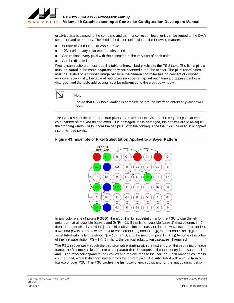
PXA3xx (88AP3xx) Processor FamilyVolume III: Graphics and Input Controller Configuration Developers Manual
Doc. No. MV-S301374-03 Rev. 2.0 Version -
Copyright © 2009 Marvell
Page 166 April 6, 2009 Released
12345678910111213141516171819202122232425262728293031323334353637383940414243444546474849505152535455565758
or 10-bit data is passed to the compand and gamma correction logic, or it can be routed to the DMA controller and to memory. The pixel substitution unit includes the following features:
Sensor resolutions up to 2560 × 2048128 pixels of any color can be substituted
Can replace every pixel with the exception of the very first of each colorCan be disabled
First, system software must load the table of known bad pixels into the PSU table. The list of pixels must be sorted in the same sequence they are scanned out of the sensor. The pixel coordinates must be relative to a cropped image because the camera controller has no concept of cropped windows. Specifically, the table of bad pixels must be remapped each time a cropping window is changed, and the table addressing must be referenced to the cropped window.
Note
Note Ensure that PSU table loading is complete before the interface enters any low-power mode.
The PSU restricts the number of bad pixels to a maximum of 128, and the very first pixel of each color cannot be marked as bad even if it is damaged. If it is damaged, the choices are to re-adjust the cropping window or to ignore the bad pixel, with the consequence that it can be used in or copied into other bad pixels.
Figure 43: Example of Pixel Substitution Applied to a Bayer Pattern
In any color plane (4 pixels RGGB), the algorithm for substitution is for the PSU to use the left neighbor if at all possible (case 1 and 5) (Pi – 1). If this is not possible (case 3) (first column, i = 0), then the upper pixel is used P(i,j - 1). This substitution can cascade in both ways (case 2, 4, and 6). If two bad pixels of one row are next to each other P(i,j) and P(i+1,j), the first bad pixel P(i,j) is substituted with its left neighbor P(i – 1,j) if i > 0, and the next bad pixel P(i + 1,j) becomes the value of the first substitution P(i – 1,j). Similarly, the vertical substitution cascades, if required.
The PSU sequences through the bad pixel table starting with the first entry. At the beginning of each frame, the first entry is loaded into a comparator that decomposes the table entry into two parts: i and j. The rows correspond to the i values and the columns to the j values. Each row and column is counted and, when both coordinates match the current pixel, it is substituted with a value from a four-color pixel PSU. The PSU caches the last pixel of each color, and for the first column, it also

Quick Capture InterfaceOperation
Copyright © 2009 Marvell Doc. No. MV-S301374-03 Rev. 2.0Version -
April 6, 2009 Released Page 167
12345678910111213141516171819202122232425262728293031323334353637383940414243444546474849505152535455565758
saves the first pixel of each color of the previous row. When the hit occurs, the next table entry is loaded into the comparator.
To indicate that there are no bad pixels, disable the PSU by clearing CIPSS[PSU_EN] (refer to Figure 108). The table entries are stored by writing to the Quick Capture Interface Pixel Substitution Buffer (CIPBUF) register in the PSU (see Table 109). Restrictions on PSU operation are as follows:
The PSU table can be reloaded only when a frame completes and the camera interface unit is idle.
Loading the table with duplicate values is illegal.Order of dead pixels must be enforced.Loading the table with the pixel list outside the frame size is illegal.
3.4.1.3 Compand and Gamma Correction (CGC)The CGC provides a three-channel lookup table (LUT) for companding and remapping data to adjust for sensor nonlinearity, brightness, contrast, and gamma. The companding operation reduces the bit depth of RAW pixel data from 10 bits to 8 bits while performing the remapping operation. A black-level clamp (BLC) sets the maximum value that is mapped to values greater than zero. CGC features are as follows:
• Three channels with 64 elements each are available for mapping, fR(x), fG(x), and fB(x)
• Programmable BLC to establish a threshold for the black level
• Programmable distribution of elements across four quadrants with linear interpolation
• RAW RGGB data can be input to the unit in natural order (RGRGRG....GBGBGB...RGRG).
During an image capture, the CGC receives either 8- or 10-bit raw data, three control signals (frame valid, line valid, and pixel clock), and two tag bits (indicating color plane) from the capture interface. The CGC uses the two tag bits to select one of the three RAM look-up tables.
Note
Note The CGC lookup table must be reloaded when the CI is disabled and re-enabled. Three Descriptors (one for each color) must be used to load the lookup table.
The CGC uses the pixel data as an address into the RAM lookup table for the color plane specified by the tag bits (see Table 84). The result of the lookup table (two 8-bit values) is the weighted linear interpolated result of the two values held in one of the three 64-element arrays. There are two modes of operation: 10-bit to 8-bit mapping, and 8-bit to 8-bit mapping.
Sixty-four elements are provided in each channel LUT to minimize error for non-linear mapping of the pixel data with gamma correction and companding operations. Providing more data points in intervals where the curvature of the transfer function is high yields a more accurate approximation, but the approximation is still too coarse to be useful. A linear interpolation technique is used to improve the approximations.
Table 84: Color Tag LUT Address Mapping
Color Tag LUT Address Space
Red 0x00-0x1F
Blue 0x20-0x3F
Green 0x40-0x5F
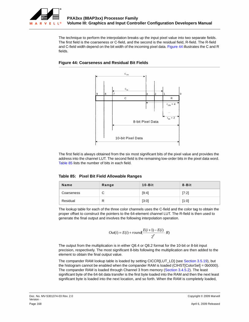
PXA3xx (88AP3xx) Processor FamilyVolume III: Graphics and Input Controller Configuration Developers Manual
Doc. No. MV-S301374-03 Rev. 2.0 Version -
Copyright © 2009 Marvell
Page 168 April 6, 2009 Released
12345678910111213141516171819202122232425262728293031323334353637383940414243444546474849505152535455565758
The technique to perform the interpolation breaks up the input pixel value into two separate fields. The first field is the coarseness or C-field, and the second is the residual field, R-field. The R-field and C-field width depend on the bit width of the incoming pixel data. Figure 44 illustrates the C and R fields.
Figure 44: Coarseness and Residual Bit Fields
The first field is always obtained from the six most significant bits of the pixel value and provides the address into the channel LUT. The second field is the remaining low-order bits in the pixel data word. Table 85 lists the number of bits in each field.
The lookup table for each of the three color channels uses the C-field and the color tag to obtain the proper offset to construct the pointers to the 64-element channel LUT. The R-field is then used to generate the final output and involves the following interpolation operation.
The output from the multiplication is in either Q8.4 or Q8.2 format for the 10-bit or 8-bit input precision, respectively. The most significant 8-bits following the multiplication are then added to the element to obtain the final output value.
The compander RAM lookup table is loaded by setting CICCR[LUT_LD] (see Section 3.5.19), but the histogram cannot be enabled when the compander RAM is loaded (CIHST[ColorSel] = 0b0000). The compander RAM is loaded through Channel 3 from memory (Section 3.4.5.2). The least significant byte of the 64-bit data transfer is the first byte loaded into the RAM and then the next least significant byte is loaded into the next location, and so forth. When the RAM is completely loaded,
Table 85: Pixel Bit Field Allowable Ranges
Name Range 10-Bit 8-Bit
Coarseness C [9:4] [7:2]
Residual R [3:0] [1:0]
8-bit Pixel Data
9 8
C R
0
r10b = 4
r9b = 3
r8b = 2
C8b
7
C9b
C10b
123
9-bit Pixel Data
10-bit Pixel Data
)2
)()1(()()( R
riEiE
roundiEiOut ⋅−++=

Quick Capture InterfaceOperation
Copyright © 2009 Marvell Doc. No. MV-S301374-03 Rev. 2.0Version -
April 6, 2009 Released Page 169
12345678910111213141516171819202122232425262728293031323334353637383940414243444546474849505152535455565758
the hardware clears CICCR[LUT_LD]. Because this bit is cleared only after the RAM is completely loaded, software must ensure that there is enough data in the transfer to fill the entire RAM (24 64-bit data transfers).
The following is the Descriptor programming model for loading the LUT:
1. Load the CGC LUT with 192 bytes of data.2. Program the Descriptor in internal SRAM with a burst size of 64.
3. Program CIDADR3 (in the CI unit to reflect the Descriptor address).4. Wait for CICCR[LUT_L] to clear (indicates that the 64 bytes are loaded into the LUT).5. Repeat this sequence, starting with step 2) until all three Descriptors are completed.
3.4.1.4 Spatial Scaling Unit (SSU)Spatial scaling is useful for variable resolutions and for managing data transfers. The scaling unit provides a high-quality scaling operation using a 3 × 3 and 5 × 5 separable kernel for 2:1 and 4:1 scaling operations. The scaling unit works only on 8-bit raw or YCbCr data. Accumulated results are truncated to 8-bit values. Features of the SSU are as follows:
2:1 or 4:1 spatial scaling of YCbCr images from a minimum size of 33 × 33 to a maximum size of 704 horizontal pixels, with no limits in the vertical axis by the sensor
2:1 or 4:1 spatial scaling of RAW RGGB data from a minimum size of 34 × 33 to a maximum size of 1280 horizontal pixels, with no limits in the vertical axis by the sensor
One register enables or bypasses the scaling unit and selects the 2:1, 4:1 scaling optionOverlapping 3- or 5-tap filter is employed in the calculation
3.4.1.4.1 Basic 2:1 and 4:1 Scaling OperationSSU scaling involves two modes: 2:1 and 4:1. The SSU performs a two-dimensional 2:1 or 4:1 reduction of the original image using two separate one-dimensional scaling processes. A three- or five-tap value finite-impulse-response (FIR) filter is used for each scaling pass. The tap coefficients are (1, 2, 1) or (1, 2, 2, 2, 1), which are the same for both dimensions, and the normalization factor is 4 and 8 for each pass. This effectively reduces a 3 × 3 or 5 × 5 overlapping pixel window down to one pixel.
Figure 45 illustrates the 2:1 scaling process in a single color plane. It shows the overlap between adjacent 3 × 3 windows. The equivalent filter coefficient matrix after the two-pass scaling is also shown. The location of the pixel assigned to the largest weight is the position of the new pixel in the scaled image. The boxes surrounding the gray pixels scope the 3 × 3 operation window. The shaded pixels indicate the location of the new pixels in the scaled image.

PXA3xx (88AP3xx) Processor FamilyVolume III: Graphics and Input Controller Configuration Developers Manual
Doc. No. MV-S301374-03 Rev. 2.0 Version -
Copyright © 2009 Marvell
Page 170 April 6, 2009 Released
12345678910111213141516171819202122232425262728293031323334353637383940414243444546474849505152535455565758
Figure 45: 2:1 Scaling Filter
The 2:1 scaling algorithm is represented mathematically in the following formula, where the scaled pixel value of the top left 3 × 3 window, R’00, is calculated as:
For the 2:1 case, the horizontal scaling pass starts with accumulating the first pixel value multiplied by one, followed by the second pixel value multiplied by 2, and finally the third pixel value multiplied by one, all accumulated with the result divided by 4 to normalize. The 4:1 uses another set of coefficients (1, 2, 2, 2, 1) and normalizes with 8 to normalize.
If the input image is RGGB and larger than 640 pixels vertically, a different scaling algorithm is used for both cases. Instead of (a + 2b + c)/4 the equation (3b + c)/4 is used for scaling 2:1. For 4:1
⎟⎟⎠
⎞⎜⎜⎝
⎛•⎟⎟
⎠
⎞⎜⎜⎝
⎛•= ∑ ∑∑ ∑
= == =
2
0
2
0
2
0
2
0
'00 /)(
i jij
j iijij RR βααβ
)1,2,1(,4/2
04/
2
0==
⎟⎟⎟
⎠
⎞
⎜⎜⎜
⎝
⎛
= ⎟⎟⎟
⎠
⎞
⎜⎜⎜
⎝
⎛
⎟⎟
⎠
⎞
⎜⎜
⎝
⎛
=•= ∑ ∑ ii
j iijRij βααα
1 2 1
2 1 2
1 2 1
2:1 Scaling Kernel
1 2 2 2 1
2 4 4 4 2
2 4 4 4 2
2 4 4 4 2
1 2 2 2 14:1 Scaling Kernel

Quick Capture InterfaceOperation
Copyright © 2009 Marvell Doc. No. MV-S301374-03 Rev. 2.0Version -
April 6, 2009 Released Page 171
12345678910111213141516171819202122232425262728293031323334353637383940414243444546474849505152535455565758
scaling the equation becomes (3c + 4d + e)/8. The horizontally scaled values are similarly computed in the vertical scaling axis. Horizontal pixels are sent to the vertical scaling process, but because the data is out of order in the sequence that is required for the computation, the math operations are performed in the order in which the data arrives (horizontal) and the intermediate accumulated results are stored in an array of accumulators. The array size is determined by the maximum number of column pixels in the scaled image.
For the overlapping filter to operate, the number of column pixels required for a single color plane is 2n + 2 for 2:1 scaling and 4n + 2 for 4:1 scaling, where n is the number of pixels per color plane of the scaled image. The use of border pixels is common in image sensors and can be either active or dark pixels. The RAW RGGB format uses the same formula, but because it has red/green and blue/green pixels interleaved on each row, a total of 2n + 2 pixel elements must be received for 2:1 scaling and 4n + 2 for the 4:1 scaling. For each formats, YCbCr 4:2:2 or RAW, the sensor must be programmed with the preferred crop window.
For example, a 320 × 240 scaled image in RAW RGGB format requires a total of 642 × 482 raw pixels from the original image. A 160 × 120 scaled image requires a total of 642 × 482 raw pixels from the original image. The sensor must be programmed with the preferred crop window. See Table 86 and Table 87.
Table 86: Summary of Scaling Formula
Capture Data Format
Scal ing Mode
Input to Camera Interface (Effect ive PPL, LPF)
Output from Scal ing Unit
Notes
RAW RGGB
2:1 (2m+2, 2n+2) (m, n) (m, n) are even numbers
RAW RGGB
4:1 (4m+2, 4n+2) (m, n) “
YCbCr 4:2:2
2:1 (2m+2, 2n+1) (m, n) “
YCbCr 4:2:2
4:1 (4m+2, 4n+1) (m, n) “
Table 87: Scaling Examples
Capture Data Format
Scal ing Mode
Image Sensor Field of View (FOV)
Image Sensor Crop Window
Output from Scaler
YCbCr 4:2:2 None 2560 × 2048 2560 × 2048 Bypassed
2:1 or 4:1 640 × 480 642 × 481 320 × 240 or 160 × 120
2:1 or 4:1 704 × 576 706 × 577 352 × 288 or 176 × 144

PXA3xx (88AP3xx) Processor FamilyVolume III: Graphics and Input Controller Configuration Developers Manual
Doc. No. MV-S301374-03 Rev. 2.0 Version -
Copyright © 2009 Marvell
Page 172 April 6, 2009 Released
12345678910111213141516171819202122232425262728293031323334353637383940414243444546474849505152535455565758
When the sensor sends data that does not meet the required formula, the unfinished calculations are cleared out on end-of-line or end-of-frame events. For example, an image input in RGGB format at 643 × 483 resolution would generate a 320 × 240 image for 2:1 scaling.
3.4.1.5 Color Synthesis Unit (CSU)The input to the color synthesis unit is always RAW 8-bit data. All image data originates with raw sensor pixel data. Each pixel has a color filter over it, passing light centered around one or more wavelengths. The image size limitation for color synthesis and color management units is 352 pixels wide, or less with spatial scaling with no limits in the vertical axis except as provided by the maximum capture resolution. A dummy line is needed at the end. The sensor can sample only a single color at each photosite, as shown in Figure 46.
Figure 46: (a) Bayer Pattern Color Filter Array (CFA) and (b) 24-Bit Color
The bandpasses are determined by the color filters and generally do not correspond to a standard color space. The combination of device-specific color representation in the spatial and spectral domains is defined as cRGB for camera RGB space. It constitutes the raw format for the image data and is the native representation of the sensed data. A single 8-bit value follows the companding operation for each photosite on the sensor. The color associated with the 8-bit value depends on the color filter material on the pixel, which in turn is associated with the pixel spatial location.
The color interpolation algorithm converts the input Bayer Pattern CFA image into a RAW 24-bit image by first interpolating the missing green at each red or blue pixel location and then interpolating the remaining red and blue pixels. The output is uncorrected RGB 8:8:8.
Four different cases arise, depending upon the presence of a measured value in the pixel location, as illustrated in Figure 47.
RAW RGGB None 2560 × 2048 2560 × 2048 Bypassed
2:1 or 4:1 1280 × 1024 1282 × 1026 640 × 512 or 320 × 256
2:1 or 4:1 704 × 576 706 × 578 352 × 288 or 176 × 144
2:1 or 4:1 640 × 480 642 × 482 320 × 240 or 160 × 120
Table 87: Scaling Examples (Continued)
Capture Data Format
Scal ing Mode
Image Sensor Field of View (FOV)
Image Sensor Crop Window
Output from Scaler
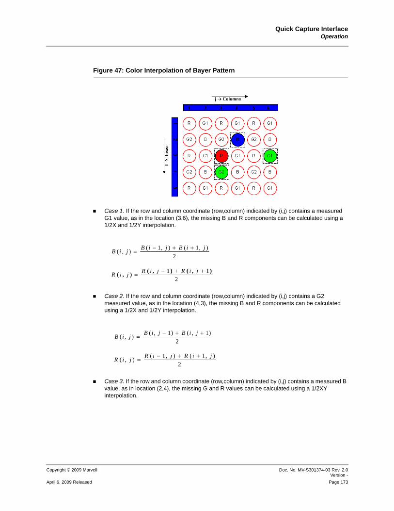
Quick Capture InterfaceOperation
Copyright © 2009 Marvell Doc. No. MV-S301374-03 Rev. 2.0Version -
April 6, 2009 Released Page 173
12345678910111213141516171819202122232425262728293031323334353637383940414243444546474849505152535455565758
Case 1. If the row and column coordinate (row,column) indicated by (i,j) contains a measured G1 value, as in the location (3,6), the missing B and R components can be calculated using a 1/2X and 1/2Y interpolation.
Case 2. If the row and column coordinate (row,column) indicated by (i,j) contains a G2 measured value, as in the location (4,3), the missing B and R components can be calculated using a 1/2X and 1/2Y interpolation.
Case 3. If the row and column coordinate (row,column) indicated by (i,j) contains a measured B value, as in location (2,4), the missing G and R values can be calculated using a 1/2XY interpolation.
Figure 47: Color Interpolation of Bayer Pattern
2
),1(),1(),(
jiBjiBjiB
++−=
2
11 ),(),(),(
++−= jiRjiRjiR
2
)1,()1,(),(
++−= jiBjiBjiB
2
),1(),1(),(
jiRjiRjiR
++−=
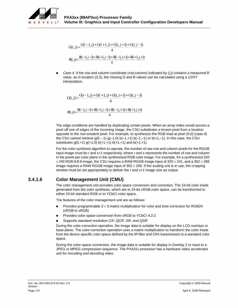
PXA3xx (88AP3xx) Processor FamilyVolume III: Graphics and Input Controller Configuration Developers Manual
Doc. No. MV-S301374-03 Rev. 2.0 Version -
Copyright © 2009 Marvell
Page 174 April 6, 2009 Released
12345678910111213141516171819202122232425262728293031323334353637383940414243444546474849505152535455565758
Case 4. If the row and column coordinate (row,column) indicated by (i,j) contains a measured R value, as in location (3,3), the missing G and B values can be calculated using a 1/2XY interpolation.
The edge conditions are handled by duplicating certain pixels. When an array index would access a pixel off one of edges of the incoming image, the CSU substitutes a known pixel from a location opposite to the non-existent pixel. For example, to synthesize the RGB triad at pixel (0,0) (case 4) the CSU cannot retrieve g(0, –1) g(–1,0) b(–1,+1) b(–1,–1) or b(+1,–1). In this case, the CSU substitutes g(0,+1) g(+1,0) b(+1,+1) b(+1,+1) and b(+1,+1).
For the color synthesis algorithm to operate, the number of raw row and column pixels for the RGGB input image must be r and s+1 respectively, where r and s represents the number of row and column in the pixels per color plane in the synthesized RGB color image. For example, for a synthesized 320 × 240 RGB 8:8:8 image, the CSU requires a RAW RGGB image input of 320 × 241, and a 352 × 288 image requires a RAW RGGB image input of 352 × 289. If the scaling unit is in use, the cropping window must be set appropriately to deliver the r and s+1 image size as output.
3.4.1.6 Color Management Unit (CMU)The color management unit provides color space conversion and correction. The 24-bit color triads generated from the color synthesis, which are in 24-bit cRGB color space, can be transformed to either 24-bit standard RGB or to YCbCr color space.
The features of the color management unit are as follows:
Provides programmable 3 × 3 matrix multiplication for color and tone correction for RGB24 (cRGB to sRGB)Provides color space conversion from cRGB to YCbCr 4:2:2
Supports standard resolution CIF, QCIF, SIF, and QSIFDuring the color-correction operation, the image data is suitable for display on the LCD overlays or base plane. The color-correction operation uses a matrix multiplication to transform the color triads from the device specific color space defined by the IR filter and CFA transmission to a standard color space.
During the color-space conversion, the image data is suitable for display in Overlay 2 or input to a JPEG or MPEG compression sequence. The PXA31x processor has a hardware video accelerator unit for encoding and decoding video.
4
)1,()1,(),1(),1(),(
−+++++−= jiGjiGjiGjiGjiG
4
)1,1()1,1()1,1()1,1(),(
++++−+−++−−= jiRjiRjiRjiRjiR
4
)1,()1,(),1(),1(),(
−+++++−=
jiGjiGjiGjiGjiG
4
)1,1()1,1()1,1()1,1(),(
++++−+−++−−= jiBjiBjiBjiBjiB

Quick Capture InterfaceOperation
Copyright © 2009 Marvell Doc. No. MV-S301374-03 Rev. 2.0Version -
April 6, 2009 Released Page 175
12345678910111213141516171819202122232425262728293031323334353637383940414243444546474849505152535455565758
3.4.1.6.1 Color and Tone Scale CorrectionThe color and tone scale correction is accomplished by first converting the non-linear data after color interpolation (each pixel in R, G, and B color planes) to linear space using the compand and gamma correction unit and then multiplying each RGB triad by a color-correction matrix. The color-correction matrix converts the pixel from the RGB color space of the image sensor to the color space of the CIR 709 primaries. The matrix multiplication is as follows:
where the coefficients Ki,j are programmable with 10-bit precision. Note that input R, G, B and output Rcorrected, Gcorrected, Bcorrected, in the equation are 8-bit data. It is sufficient to maintain two decimal places of precision for the matrix coefficients and to require that the row sum be unity, that is K0,0+ K0,1+K0,2 = K1,0+ K1,1+K1,2 = K2,0+ K2,1+K2,2 = 1.
The LCD panel is assumed to have an sRGB-defined gamma and viewing conditions.
The coefficients for color correction are supplied by the image-sensor manufacturers so that developers can generally avoid the complexities of generating the values. Coefficients are precalculated and converted into a fixed-point format. The coefficients for the color-correction matrix are 10-bit signed 2’s-complement numbers. Three bits are used for the signed-integer portion of the number, and seven bits are used for the fractional portion. The numbers can range from –4.000 to +3.992. Figure 48 shows the fractional representation of the color-correction coefficients.
Figure 48: Fractional Format for Color-Correction Coefficients
The multiplication operations described by the preceding equation involve signed fractional and unsigned integer operands. The final output values are unsigned 8-bit values in the range from 0 to 255. Maintain the decimal place when converting the final results to the preferred accuracy.
The multiplication of a signed 10-bit 2’s-complement fractional by an 8-bit unsigned value produces a signed 18-bit fractional result. Three 10-bit-by-8-bit multiplications are performed for each output color component, (Rcorrected,Gcorrected, and Bcorrected). The three values are added together to produce a 19-bit signed fractional result. Because the coefficients are represented by seven fractional bits, rounding on bit position six followed by extraction of bits [14:7] produces the preferred output values. Figure 49 illustrates the extraction of the final result for each color component. The output is unsigned and constrained in the range from 0 to 255.
Rcorrected
Gcorrected
Bcorrected
K0 0, K0 1, K0 2,
K1 0, K1 1, K1 2,
K2 0, K2 1, K2 2,
R
G
B⎝ ⎠⎜ ⎟⎜ ⎟⎜ ⎟⎛ ⎞
•=
9 8 7 6 5 4 3 2 1 0
fractional partsign bit whole part
Color Correction Coefficients Ki,jSigned Fraction Representation

PXA3xx (88AP3xx) Processor FamilyVolume III: Graphics and Input Controller Configuration Developers Manual
Doc. No. MV-S301374-03 Rev. 2.0 Version -
Copyright © 2009 Marvell
Page 176 April 6, 2009 Released
12345678910111213141516171819202122232425262728293031323334353637383940414243444546474849505152535455565758
Figure 49: Extraction of Final Result for Each Color Component
3.4.1.6.2 Color Space Conversion (CSC)The color space conversion (CSC) from RGB to YCbCr is based on the ITU-R BT.601 standard. It has one format output: 4:2:2. The matrix representation is as follows:
where the coefficients Ki,j are programmable with 10-bit precision. The multiplications must maintain a minimum of 8 bits of fractional data with the final results rounded to the preferred accuracy.
The coefficients for color-space conversion are precalculated and converted into a fixed-point format. The coefficients for the color-correction matrix are 10-bit signed 2’s-complement numbers. Two bits are used for the signed integer portion of the number, and eight bits are used for the fractional portion. The numbers can range from –2.000 to +1.996.
Figure 50: Fractional Representation for CSC Coefficients
The multiplication operations described by the preceding equation involve signed fractional and unsigned integer operands. The final output values are unsigned 8-bit values in the range from 0 to 255. Maintain the decimal place when converting the final results to the preferred accuracy.
The multiplication of a signed 10-bit 2’s-complement fractional number by an 8-bit unsigned value produces a signed 18-bit fractional result. Three 10-bit by 8-bit multiplications are performed for each output color component (Y, Cb, and Cr). The three values are added together producing a 19-bit signed fractional result followed by the addition of the constants 16 or 128, as indicated. Since the coefficients are represented by eight fractional bits, rounding on bit position 7 followed by extraction of bits [15:8] produces the preferred output values. Figure 51 illustrates the extraction of the final result for each of the channels.
18 17 16 15 14
sign bit
7 6 5 4 3 2 1 0
whole part1 0 0 0 0 0 0
fractional part
+
19-bit Signed Fractional Valueresulting from R*Ki,0+G*Ki,1+B*Ki,2
8-bit Result
Y
Cr
Cb
K0 0, K0 1, K0 2,
K1 0, K1 1, K1 2,
K2 0, K2 1, K2 2,
R
G
B
16
128
128
+•=
9 8 7 6 5 4 3 2 1 0
fractional partsign bit whole part
Color Space Conversion Coefficients Ki,jSigned Fraction Representation

Quick Capture InterfaceOperation
Copyright © 2009 Marvell Doc. No. MV-S301374-03 Rev. 2.0Version -
April 6, 2009 Released Page 177
12345678910111213141516171819202122232425262728293031323334353637383940414243444546474849505152535455565758
Figure 51: Extraction of Final Result for CSC
In RGB-to-YCbCr 4:2:2 format, the Cr and Cb channels are subsampled 2:1 in the horizontal dimension with the full vertical resolution maintained. The chroma subsampling for the 4:2:2 format is illustrated in Figure 52.
Figure 52: YCbCr 4:2:2 Chroma Sub-Sampling in Horizontal Dimension
In Figure 52, Iin and Iout represent the chrominance data before and after sub-sampling, and cij represents the chrominance samples at the location (i,j) within the image frame.
The following relationship for a M × N array is used to deal with the boundary problem of the down-sampling method.
18 17 16 15
sign bit
7 6 5 4 3 2 1 0
whole part 1 0 0 0 0 0 0
fractional part
+
19-bit Signed Fractional Value resulting fromR*Ki,0+G*Ki,1+B*Ki,2+ Constant
8-bit Result
8
0
Rounding Constant
1 0 0 0 0
1 0 0 0 0 0 0 0
Y = R*K0,0+G*K0,1+B*K0,2 + 16
Cb = R*K1,0+G*K1,1+B*K1,2 + 128
Cr = R*K2,0+G*K2,1+B*K2,2 + 128
Constants 16 and 128 are unsigned integers
Iin
C00 C01 C02 C03
C10 C11 C12 C13
C20 C21 C22 C23
C30 C31 C32 C33
=
Iout
C00 C01+
2--------------------------
C02 C03+
2--------------------------
C10 C11+
2--------------------------
C12 C13+
2--------------------------
C20 C21+
2--------------------------
C22 C23+
2--------------------------
C30 C31+
2--------------------------
C32 C33+
2--------------------------
=
I m N 1+,( ) I m N,( ) for 0 m M≤ ≤=

PXA3xx (88AP3xx) Processor FamilyVolume III: Graphics and Input Controller Configuration Developers Manual
Doc. No. MV-S301374-03 Rev. 2.0 Version -
Copyright © 2009 Marvell
Page 178 April 6, 2009 Released
12345678910111213141516171819202122232425262728293031323334353637383940414243444546474849505152535455565758
The last row and column are effectively duplicated using this approach.
Note
Note The coefficients are loaded only at the beginning of a frame. Any change in the coefficient values during the frame take effect only at the start of next frame.
3.4.2 4:2:0 Downsampling (PXA31x processor only)Data conversion from YCbCr 4:2:2 to YCbCr 4:2:0 uses the decimation algorithm by dropping Cb and Cr pixels on odd rows. The decimation is allowed on the following data streams:
YCbCr 4:2:2 input stream either scaled or unscaled RAW input stream converted to YCbCr 4:2:2 either going through the scaling unit or bypassing the scaling unit.
3.4.3 Operating ModesThe the Quick Capture Interface operating modes are listed in Table 88, with the number of bits required for the parallel (P) data bus for each of the modes. The designation 8P and 10P refers to 8- and 10-bit parallel connections.
In Master mode, the sensor must be programmed for synchronization timing and frame rate, and possibly additional parameters associated with exposure control and image processing.
3.4.3.1 Master-Parallel (MP) Internal Synchronization ModeThe Master-Parallel mode of operation requires a parallel data-bus interface, a clock, and two control signals for frame timing. In this mode, the sensor is programmed for an exposure time and frame rate through the I2C serial-control interface. Acquisition of data from the sensor is initiated by transitions based on the state of the CIF_HSYNC and CIF_VSYNC signals. Several programmable wait states (Figure 53) are introduced for any required variation in delay from signal transitions to valid data.
I M 1+ n,( ) I M n,( ) for 0 n N≤ ≤=
Table 88: Quick Capture Interface Modes of Operation
Mode Name Mode Data Bus:Paral lel (P)
Synchronizat ion Signals
Definition
Master-parallel MP 8P, 10P CIF_HSYNCCIF_VSYNC
The image sensor internally generates the synchronization signals. The interface to the sensor is a parallel data bus either 8 or 10 bits wide.
Slave-parallel SP 8P,10P CIF_HSYNCCIF_VSYNC
The processor internally generates the synchronization signals. The interface to the sensor is a parallel data bus either 8 or 10 bits wide.

Quick Capture InterfaceOperation
Copyright © 2009 Marvell Doc. No. MV-S301374-03 Rev. 2.0Version -
April 6, 2009 Released Page 179
12345678910111213141516171819202122232425262728293031323334353637383940414243444546474849505152535455565758
Figure 53: Master-Parallel (MP) Internal Synchronization ModeMaster-Parallel (MP)
State Diagram
After the Quick Capture Interface is enabled, the capture sequence is activated as follows:
1. The CIF_VSYNC signal transitions to indicate that a frame readout is about to occur. 2. The state machine transitions to the BEGIN_FRAME_WAIT state and then waits for the
Beginning of Frame Wait (BFW) line clocks (CIF_HSYNC). 3. After this BFW count elapses, another CIF_HSYNC assertion brings the state machine to
BEGIN_LINE_WAIT state. 4. The master state machine waits for BLW pixel clock cycles before moving on to the
ACTIVE_DATA_CAPTURE state.Counters are maintained for both the pixels-per-line (PPL) and the lines per frame (LPF). The sensor’s number of rows and columns are synchronized with these counters. Wait states are skipped if the corresponding delay values (BFW and BLW) are programmed as zeros. The state machine goes into the idle state when the LPF and PPL counters reach zero and the active data capture stops.
3.4.3.2 JPEG Mode (PXA31x processor only)In JPEG mode, there is no notion of pixels, so the PPL (pixels per line) and LPF (pixels per frame) values are ignored. The JPEG stream uses packets of varying length. A JPEG capture is in progress as long as the VSYNC signal is asserted. When a complete stream is captured, the VSYNC signal asserts. The HSYNC signal is used to delimit a JPEG packet and is asserted when the current data being captured is valid. If HSYNC is asserted when VSYNC is deasserted, an error has occurred.
Enabling JPEG ModeWhen enabling JPEG mode, it is possible that the first frame may contain data from the previous capture or trailing bytes. This will show as errors in the first JPEG frame capture. The imaging pipe may have bytes of data that will need to be flushed out of the chain.
To perform this task, software should enable the JPEG mode and capture one frame and then discard it. The first frame that is discarded does not have to be a full frame size. The interface could be configured to a much smaller frame size to reduce the capture time for the discarded frame.
The CIFR0[RESETF] is used to reset the FIFO pointers, it does not flush the imaging pipe. The first frame must be discarded.
BFW = Begining of Frame Wait
PPL = Pixels Per LineBLW = Begining of Line Wait
LPF = Lines Per Frame
Idle
Begin FrameWait
CIF_VSYNC = 1
ActiveData
Capture
Begin LineWait
PPL--
CIF_HSYNC= 1
BLW--
CIF_HSYNC = 1
BFW--
LPF --
PPL = 0 & LPF = 0PPL = 0 andLPF = 0
Idle

PXA3xx (88AP3xx) Processor FamilyVolume III: Graphics and Input Controller Configuration Developers Manual
Doc. No. MV-S301374-03 Rev. 2.0 Version -
Copyright © 2009 Marvell
Page 180 April 6, 2009 Released
12345678910111213141516171819202122232425262728293031323334353637383940414243444546474849505152535455565758
When the CIJPEG[JPEG_EN] is set (0b1) the camera interface will start to read in data when VSYNC and HYNC are asserted. The timing of when software enables JPEG mode is critical. Regardless of why the synch signals assert, the interface will start to read in the data on the pixel bus.
This really highlights the necessity for proper management of enabling the quick capture interface. Good programming practice would be that software first configures the sensor followed by the quick capture interface. This will omit any potential glitches on the bus from being interpreted as JPEG data.
Switching from RAW into JPEG Capture ModeMarvell recommends that when switching between modes such as; enabling JPEG mode afer a RAW capture, the CICRO[DIS] bit is set, which allows the current frame capture to complete. Once this is complete the CISR[CDD] status bit is set. Then software should start the JPEG capture with CIJPEG[ENB]. This method will ensure that the JPEG capture is not started while the last frame of the RAW data capture is still active.
Note
Note If software does not wait for the last transaction to completely finish, the data stream will be read in as JPEG data.
Software may also force a quick shutdown of the camera interface by setting CICR0[ENB]. Data acquisition stops immediately, regardless of whether the current frame has completed. The CISR[CQD] status bit is set.
JPEG Frame Length and Methods to Capture FramesThe number of captured bytes can be read from CIJPEG[BYTE_CNT]. This bitfield shows total bytes transferred between enabling and disabling JPEG mode CIJPEG[JPEG_EN]. The BYTE_CNT is only enabled when JPEG_EN is set.
The BYTE_CNT operates well for single frame captures. Also, software has the ability to use the DMA length bitfield for the same purpose. To calculate the amount of bytes on a frame by frame basis using DMA Descriptors, software should perform the following steps:
The CIDCMD[LENGTH] is set to the maximum amount of bytes per frameThe capture starts and the LENGTH value is decremented for every byte transferred
The CISR[EOFX] indicates the frame boundary and an interrupt is sent to the coreSoftware must then read the LENGTH value and compare it with the original value to report a frame length (size) in bytes
However, for multiple back to back JPEG frame captures, it is not possible to use these two options because the real time nature of multiple frame captures would require the interrupts and the servicing of theinterrupts to calculate frame size, to be instant. The LENGTH bitfield would be constantly changing without software knowing what frame the value is applicable too.
The JPEG header and footer should be encoded in to the data stream by the camera sensor. Some sensors must be configured for this feature. Consult the sensor datasheet for details. Software must search the buffer for these markers in order to calculate the frame size(s). Also, the location of these markers is required for further tasks such as preview or editing the picture (frames).
The CIDMA can be configured in multiple ways. SIngle Descriptors or multiple Descriptors may be used however, branching is only supported for the last Descriptor in a frame.
To summarize the two different length or byte count fields:
CIJPEG[BYTE_CNT] indicates total JPEG bytes since the last Write to CIJPEG register

Quick Capture InterfaceOperation
Copyright © 2009 Marvell Doc. No. MV-S301374-03 Rev. 2.0Version -
April 6, 2009 Released Page 181
12345678910111213141516171819202122232425262728293031323334353637383940414243444546474849505152535455565758
CIDCMDx[LENGTH] indicates the length of the current frame Descriptor for that channel.
Note
Note When setting up buffer size or DMA length for JPEG capture, use the maximum possible frame size which would be the maximum camera sensor resolution.
JPEG EOF and SOFThe EOF (end of frame) and SOF (start of frame) are almost identical for JPEG and Non-JPEG modes. The EOF and SOF are generated as described below;
Non-JPEG mode
EOF is generated whenever VSYNC is deasserted.SOF is generated whenever VSYNC is asserted at the beginning of a frame.
JPEG mode
EOF is delayed (and thus the interrupt) by one cycle whenever VSYNC is deasserted. SOF is generated whenever VSYNC is asserted at the beginning of a frame.
Note
Note CISR[EOF] indicates EOF at the pixel bus. All lines of the frame are captured. CISR[EOFX] indicates EOF transferred to memory. CISR[SOF] identifies the start of the frame.
3.4.3.3 Slave-Parallel (SP) External Synchronization ModeThe Slave-Parallel mode of operation is available as an option with several image sensors. When used in this mode, the Quick Capture Interface must provide the CIF_HSYNC and CIF_VSYNC signals to the sensor. The relationship between the timing must be kept exact, because the sensor uses the horizontal sync to synchronize the data acquisition. The state diagram for the SP modes is illustrated in Figure 54.
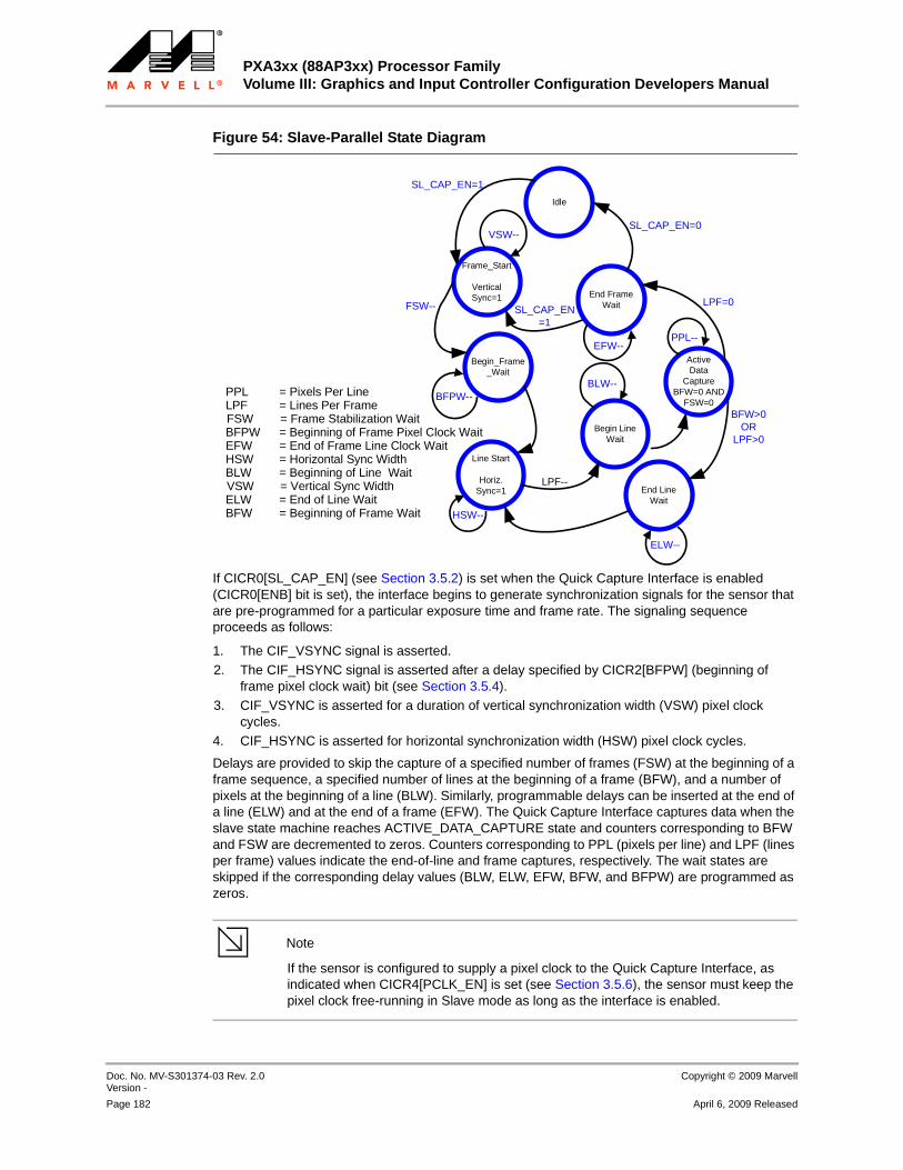
PXA3xx (88AP3xx) Processor FamilyVolume III: Graphics and Input Controller Configuration Developers Manual
Doc. No. MV-S301374-03 Rev. 2.0 Version -
Copyright © 2009 Marvell
Page 182 April 6, 2009 Released
12345678910111213141516171819202122232425262728293031323334353637383940414243444546474849505152535455565758
Figure 54: Slave-Parallel State Diagram
If CICR0[SL_CAP_EN] (see Section 3.5.2) is set when the Quick Capture Interface is enabled (CICR0[ENB] bit is set), the interface begins to generate synchronization signals for the sensor that are pre-programmed for a particular exposure time and frame rate. The signaling sequence proceeds as follows:
1. The CIF_VSYNC signal is asserted.2. The CIF_HSYNC signal is asserted after a delay specified by CICR2[BFPW] (beginning of
frame pixel clock wait) bit (see Section 3.5.4). 3. CIF_VSYNC is asserted for a duration of vertical synchronization width (VSW) pixel clock
cycles.4. CIF_HSYNC is asserted for horizontal synchronization width (HSW) pixel clock cycles.
Delays are provided to skip the capture of a specified number of frames (FSW) at the beginning of a frame sequence, a specified number of lines at the beginning of a frame (BFW), and a number of pixels at the beginning of a line (BLW). Similarly, programmable delays can be inserted at the end of a line (ELW) and at the end of a frame (EFW). The Quick Capture Interface captures data when the slave state machine reaches ACTIVE_DATA_CAPTURE state and counters corresponding to BFW and FSW are decremented to zeros. Counters corresponding to PPL (pixels per line) and LPF (lines per frame) values indicate the end-of-line and frame captures, respectively. The wait states are skipped if the corresponding delay values (BLW, ELW, EFW, BFW, and BFPW) are programmed as zeros.
Note
Note If the sensor is configured to supply a pixel clock to the Quick Capture Interface, as indicated when CICR4[PCLK_EN] is set (see Section 3.5.6), the sensor must keep the pixel clock free-running in Slave mode as long as the interface is enabled.
Idle
Begin_Frame_Wait
BFW>0OR
LPF>0
ActiveData
CaptureBFW=0 AND
FSW=0
Begin LineWait
PPL--
ELW--
HSW--
LPF=0
VSW--
BLW--
End Frame Wait
Frame_Start
Vertical Sync=1
End Line Wait
Line Start
Horiz. Sync=1
EFW--
LPF--
BFPW--
FSW--
SL_CAP_EN=1
SL_CAP_EN=0
SL_CAP_EN=1
BFPW = Beginning of Frame Pixel Clock Wait
PPL = Pixels Per Line
HSW = Horizontal Sync Width
LPF = Lines Per FrameFSW = Frame Stabilization Wait
VSW = Vertical Sync WidthBLW = Beginning of Line Wait
BFW = Beginning of Frame WaitELW = End of Line Wait
EFW = End of Frame Line Clock Wait

Quick Capture InterfaceOperation
Copyright © 2009 Marvell Doc. No. MV-S301374-03 Rev. 2.0Version -
April 6, 2009 Released Page 183
12345678910111213141516171819202122232425262728293031323334353637383940414243444546474849505152535455565758
3.4.4 Clock GenerationThe processor has three Quick Capture Interface clock domains: system bus clock, capture interface clock (CICLK), and camera pixel clock (CIF_PCLK/CIF_MCLK). The sensor can use either of the following two clocks as the master clock to generate the sensor pixel clock (CIF_PCLK):
CIF_MCLK supplied by the Quick Capture Interface (Slave mode)Local sensor clock (Master mode)
To generate the sensor master clock (CIF_MCLK) of programmable frequency, the clock generator divides the input clock, CICLK, by the programmed clock-divider value CICR4[DIV]. CICLK frequency and the various frequency settings are as shown in the clocks and power management chapters. The following equation gives the CIF_MCLK frequency.
However, the pixel clock supplied by the sensor to the Quick Capture Interface cannot exceed a frequency of 48 MHz and cannot be greater than one quarter the frequency of CICLK for the PXA30x processor and PXA32x processor. The pixel clock supplied by the sensor to the Quick Capture Interface cannot exceed a frequency of 96 MHz and cannot be greater than half the frequency of CICLK.
A wide range of frequencies are possible for CIF_PCLK. The following frequencies are supported: 26/13/6.5/3.25 MHz; 48/24/12/6/3 MHz.The system bus clock domain is eliminated in the PXA31x processor. The following additional frequencies are also supported in the PXA31x processor: 96 MHz, 78 MHz and 50 MHz.
3.4.5 FIFO OperationThe input data from the sensor is packed into the required format and written into the FIFO. The timing references for capture are provided by CIF_HSYNC/CIF_VSYNC inputs.
The capture interface has three separate FIFOs that act as temporary storage for the captured video/image data. The Read channel uses the fourth FIFO to load the companding LUT and also to send the Histogram data to memory. Table 89 lists the storage capacity and use for each FIFO. When the Quick Capture Interface operates in planarized YCbCr mode, the channel 0 FIFO is used to store the Y component of data, channel 1 FIFO for the Cb component, and channel 2 FIFO for the Cr component. In other operating modes, the channel 0 FIFO is the only FIFO used.
All FIFOs are read-only. Any Write to the FIFOs results in a system-bus error. For pixel data that is not YCbCr, the first three FIFOs are combined into one FIFO.
MCLKCICLK
2 DIV 1+( )----------------------------=
Table 89: FIFO Operation Data
FIFO Storage Capacity (PXA30x)
Storage Capacity (PXA31x)
In Planarized YCbCr Mode
Other Modes
Channel 0 24 × 8 bytes 248 × 8 bytes Y component All components
Channel 1 12 × 8 bytes 124 × 8 bytes Cb component Not used
Channel 2 12 × 8 bytes 124 × 8 bytes Cr component Not used
Channel 3 16 × 8 bytes 16 × 8 bytes Companding LUT and histogram data

PXA3xx (88AP3xx) Processor FamilyVolume III: Graphics and Input Controller Configuration Developers Manual
Doc. No. MV-S301374-03 Rev. 2.0 Version -
Copyright © 2009 Marvell
Page 184 April 6, 2009 Released
12345678910111213141516171819202122232425262728293031323334353637383940414243444546474849505152535455565758
3.4.5.1 FIFO Data PackingWhen an end of frame is encountered during data capture, the remaining bits in the FIFO entry after the last data is written are stuffed with zeros. For example, if the last sample of a frame occupies byte 0 of the 8-byte FIFO entry, bytes 1 through 7 are written with zeros. The first valid data of the next frame is loaded to the next FIFO entry. Zero stuffing at the end of frame takes a finite time that depends on the last valid byte position and whether planarized YCbCr mode is enabled. If the next frame capture starts before zero stuffing of the previous frame is complete, incorrect Quick Capture Interface operation can result.
3.4.5.2 DMA Data Transfers from FIFOsThe QCI-dedicated four-channel DMA uses three channels to write processed data to memory and one channel to write and read statistical data to/from memory. The Channel 0 FIFO has a programmable threshold level specified by CIFR[THL_0] (see Section 3.5.26). Threshold levels of Channel 1, Channel 2, and Channel 3 FIFOs are 32 bytes.
3.4.5.2.1 Writes to MemoryWhen a FIFO reaches threshold level, the DMA controller transfers a burst of data from the FIFO to the destination address specified in the Quick Capture Interface DMA Descriptor. The Quick Capture Interface DMA Source Address register (see Section 3.5.28.3) should point to CIBR0, CIBR1, CIBR2, or CIBR3, depending on which of the DMA channels is serviced.
The DMA Descriptors must be programmed to transfer the preferred number of bytes. In planarized YCbCr mode, individual DMA channels should be programmed to transfer the required number of bytes for each component. The number of bytes in the Quick Capture Interface FIFOs corresponding to a frame is always a multiple of 8 bytes, and the DMA controller should read the entire frame data including padded zeros (if any) before moving on to read data corresponding to the next frame. The programming model for using the Quick Capture Interface DMA controller is as follows:
1. Program the CIDADRx register with the Descriptor address to be fetched.2. Set the preferred values in the control registers and DMA Control/Status register (CIDCSRx).
3. When a FIFO has data, the Descriptor is fetched and loads the CITADRx, CISADRx, and CICMDx registers with appropriate values.
4. After the Descriptor is fetched when the FIFO threshold is reached, the data transfers occur until the length field in CICMDx is zero.
3.4.5.2.2 Reads from MemoryChannel 3 is the only channel that performs Reads from memory. This channel reads compand data for the compander lookup table. When the QCI software driver initiates a request for data, the dedicated DMA controller transfers data from a memory address space specified in the DMA Descriptor. The Quick Capture Interface DMA Target register points to the CIBR3 address. The received data is put into CIBR3, where the data is transferred either to the histogram or compander RAM. Fetched data can be transferred in a split transaction, which is discussed further in the DMA chapter.
The programming model for using the Quick Capture Interface DMA is as follows:
1. Program the CIDADR3 register with the Descriptor address to be fetched.2. Set the preferred values in the control registers and DMA Control/Status register (CIDCSR3).
3. When CICCR[LUT_LD] is set, the Descriptor is fetched and loaded into the CISADR3, CITADR3, CIDADR3, and CICMD3 registers with appropriate values.
For compander lookup table loads, the next CIDADR3 register points to the same Descriptor location or the histogram Descriptor address if the histogram is to be enabled.

Quick Capture InterfaceOperation
Copyright © 2009 Marvell Doc. No. MV-S301374-03 Rev. 2.0Version -
April 6, 2009 Released Page 185
12345678910111213141516171819202122232425262728293031323334353637383940414243444546474849505152535455565758
4. After the Descriptor is fetched, the data is fetched from memory until the length field in the CICMDx is zero. If the CICMD3[EOF] is high, then CIFSR[EOF] is set, causing an interrupt.
3.4.5.3 Overflow HandlingTwo different types of FIFO overflow conditions can occur for the Quick Capture Interface.
If it occurs when GCU/LCD handshaking is active, software handles the overflow. The current frame is dropped and hardware waits for new frame. If it occurs when GCU/LCD handshaking is not active, DMA transfers are not occurring frequently enough. Software handles this type of overflow condition.
The programming model for the Quick Capture Interface DMA overflow is as follows:
1. Clear CICR0[FOM] to enable FIFO overflow interrupts.
2. Hardware sets CIFSR[IFO_x] high when an overflow in the FIFO occurs, causing the interrupt.3. Set CICR0[DIS] to complete the current frame and stop capturing any new frames. After the
DMA controller reads the final pixel, CISR[CDD] is set, which causes an interrupt if CICR0[CDM] is cleared.
4. Clear CICR0[ENB] so that the interface can enter Sleep mode. 5. Program the CIDADRx register and set the CICR0[ENB] bit to capture a new frame.
If CICCR[EN] is set before the interface enters Sleep mode, the bit is now cleared and LUT needs to be loaded before the interface is enabled.
3.4.5.4 Trailing BytesWhen the number of samples in the FIFO is less than the FIFO trigger-threshold level and no additional data is received, the remaining bytes are called trailing bytes. The Quick Capture Interface uses a timeout-based request mechanism to handle trailing bytes. A timeout condition exists when the FIFO level is below its trigger level, and the FIFO is idle for a period of time defined by the value programmed in the Quick Capture Interface Timeout register (Section 3.5.7). The timeout counter is reset when a new data sample is written to the FIFO or there is a Read from the FIFO. When all three Quick Capture Interface FIFOs are used (in planarized YCbCr mode), the timeout counter starts counting after the last data sample is written to the FIFO and is reset only after a Read from any of the FIFOs. When a timeout occurs, the FIFO timeout (CISR[FTO]) bit is set, and an interrupt request is sent if unmasked in CICR0. FIFO level values in the Quick Capture Interface FIFO Control register (Section 3.5.26) can be Read to determine how many bytes remain in the FIFOs. If a timeout is detected, the Quick Capture Interface FIFO requests DMA transfers even though the FIFO threshold is not reached and continues to request until the FIFOs are empty. Ensure that all trailing bytes are transferred by programming the Descriptor chain to handle the entire frame.
Note
Note When the Quick Capture Interface is disabled by clearing CICR0[ENB], data capture immediately stops and a trailing-byte situation can arise. Clear the data in the FIFOs by resetting the pointers to the FIFO (set CIFR0[RESETF]).
Note
Note If slow devices are used on the DFI, the interface can be blocked from transferring data for over 14μs, and the output FIFOs overflow if the capture rate is above a certain frequency. To prevent overflow, the Static Memory Controller (SMC) must not be accessed during a capture.

PXA3xx (88AP3xx) Processor FamilyVolume III: Graphics and Input Controller Configuration Developers Manual
Doc. No. MV-S301374-03 Rev. 2.0 Version -
Copyright © 2009 Marvell
Page 186 April 6, 2009 Released
12345678910111213141516171819202122232425262728293031323334353637383940414243444546474849505152535455565758
3.4.6 Pixel FormatsQuick Capture Interface captures the RAW and YCbCr 4:2:2 video sampling formats.
3.4.6.1 RAW Pixel Data FormatsAll image data originates with the RAW sensor pixel data. Each pixel has a color filter over it, passing light centered around one (or more) wavelength. As received from the sensor, each pixel has 8 or 10 bits of accuracy. The most common color filter array is the Bayer pattern that interleaves red and green pixels on the even/odd rows, and blue and green pixels on the odd/even rows.
3.4.6.2 RAW 8-Bit Data FormatThe RAW 8-bit sensor data must be processed further before display or encode. The data type for the required processing is 8-bit unsigned integer. The 8-bit data is packed into 32-bit words prior to storage. No tag bits specify the color components with RAW image capture. See Table 90.
3.4.6.3 RAW 10-Bit Data FormatThe RAW 10-bit sensor data must be processed further before display or encode. The data type for the required processing is 16-bit unsigned integer. The 10-bit data is packed into 16-bit half words prior to storage. No tag bits specify the color components with RAW image capture. The upper 6 bits of the 16-bit word are unused. The pixel format for 10-bit RAW data capture is illustrated in Table 91.
Table 90: Memory Organization for RAW 8-Bit Data
Bit 7 6 5 4 3 2 1 0
8 bits/pixel Encoded Pixel Data
Memory Organizat ion for Li t t le Endian
Bit 31 24
23 16 15 8 7 0
Base + 0x0
Pixel 3 Pixel 2 Pixel 1 Pixel 0
Base + 0x4
Pixel 7 Pixel 6 Pixel 5 Pixel 4
Table 91: Memory Organization for RAW 10-Bit Data
Bit15
14
13
12
11
10
9 8 7 6 5 4 3 2 1 0
16 bits/pixel Unused Encoded Pixel Data
Memory Organizat ion
Bit 31 16 15 0
Base + 0x0
Pixel 1 Pixel 0
Base + 0x4
Pixel 3 Pixel 2

Quick Capture InterfaceOperation
Copyright © 2009 Marvell Doc. No. MV-S301374-03 Rev. 2.0Version -
April 6, 2009 Released Page 187
12345678910111213141516171819202122232425262728293031323334353637383940414243444546474849505152535455565758
3.4.6.4 Preprocessed YCbCr Pixel Data FormatsThe YCbCr format complies with the ITU-R BT.656 format and is also used for input to MPEG and JPEG compression sequences. This format, when provided by the image sensor, can be directly displayed and can also be directly input into the compression engine. In the YCbCr planar format, the Y, Cb, and Cr components are stored as three separate arrays.
3.4.6.5 Data Capture Sequence for YCbCr FormatsThe YCbCr 4:2:2 data is presented across a parallel interface. This format has a horizontal subsampling interval of 2. There are two luminance values for each chrominance pair. The data sequence for an 8-bit interface is illustrated in Table 92. Program CICR1[PPL] to prove complete chrominance pairs for YCbCr 4:2:2 (even number of pixels per line).
3.4.6.5.1 4:2:0 (PXA31x processor only) and 4:2:2 YCbCr Video Planar FormatThe processor supports the acquisition of YCbCr 4:2:2 data and the storage of pixel data in planar format. The planar format requires the luminance and chrominance planes to be stored in separate locations in memory. The memory organization for the planar format is illustrated in Table 93. The memory required for the luminance (Y) data is twice as large as the memory required for the red chrominance (Cr) or blue chrominance (Cb).
Table 92: 8-Bit Data Capture Sequence for YCbCr 4:2:2 Color Space
Data Bus YCbCr 4:2:2 Byte Sequence
CIF_DD7 Cb07 Y07 Cr07 Y17 Cb27 Y27 Cr27 Y37
CIF_DD6 Cb06 Y06 Cr06 Y16 Cb26 Y26 Cr26 Y36
CIF_DD5 Cb05 Y05 Cr05 Y15 Cb25 Y25 Cr25 Y35
CIF_DD4 Cb04 Y04 Cr04 Y14 Cb24 Y24 Cr24 Y34
CIF_DD3 Cb03 Y03 Cr03 Y13 Cb23 Y23 Cr23 Y33
CIF_DD2 Cb02 Y02 Cr02 Y12 Cb22 Y22 Cr22 Y32
CIF_DD1 Cb01 Y01 Cr01 Y11 Cb21 Y21 Cr21 Y31
CIF_DD0 Cb00 Y00 Cr00 Y10 Cb20 Y20 Cr20 Y30
Y - Pixel Components
0 1 2 3
Cb,Cr -Pixel Components
0,1 2,3
Byte Sequence
0 1 2 3 4 5 6 7

PXA3xx (88AP3xx) Processor FamilyVolume III: Graphics and Input Controller Configuration Developers Manual
Doc. No. MV-S301374-03 Rev. 2.0 Version -
Copyright © 2009 Marvell
Page 188 April 6, 2009 Released
12345678910111213141516171819202122232425262728293031323334353637383940414243444546474849505152535455565758
3.4.7 Frame SynchronizationProper synchronization between the Quick Capture Interface, the 2D graphics controller unit (GCU), and the LCD controller minimizes or eliminates dropped frames. For display on the LCD, a frame is either displayed as captured or is rotated by the GCU.
3.4.7.1 Frame RotationWhen the Quick Capture Interface is gathering data in Landscape/Portrait mode and the LCD must display the data as portrait/landscape, a rotation is required on every captured frame. The GCU rotates the captured frame before displaying it to the LCD. This rotation requires a three-buffer solution in memory. Therefore, interrupts are needed for proper handshaking between the three blocks. Create the GCU incoming instruction so that the sequence of events is as follows:
1. Configure the Quick Capture Interface Descriptor registers and enable CICR0[GCU_EN], as described in Section 3.5.2.
2. The Quick Capture Interface captures the first frame and transfers the frame to memory (buffer 1) as usual. After the first frame is transferred, the frame-complete interrupt is generated for the GCU.
3. The Quick Capture Interface captures the second frame and begins transferring the frame to the next memory space (buffer 2).
4. The GCU reads the data in buffer 1 and stores the rotated information in the third memory space (buffer 3).
5. When the second frame is completely captured, the Quick Capture Interface waits for the GCU to clear CISR[EOFX].
Table 93: Memory Organization for 4:2:0 (PXA31x processor only) and 4:2:2 YCbCr Planarized Format
Luminance Channel (Y) Memory Organizat ion
Bit 31 24 23 16 15 8 7 0
Base + 0x00
Y Sample 4 (pixel 4) Y Sample 3 (pixel 3) Y Sample 2 (pixel 2) Y Sample 1 (pixel 1)
Base + 0x04
Y Sample 8 (pixel 8) Y Sample 7 (pixel 7) Y Sample 6 (pixel 6) Y Sample 5 (pixel 5)
Chrominance Channel (Cr) Memory Organization
31 24 23 16 15 8 7 0
Base + K + 0x00
Cr Sample 4 (pixel 7) Cr Sample 3 (pixel 5) Cr Sample 2 (pixel 3) Cr Sample 1 (pixel
1)
Base + K + 0x04
Cr Sample 8 (pixel 15) Cr Sample 7 (pixel 13) Cr Sample 6 (pixel 11) Cr Sample 5 (pixel
9)
Chrominance Channel (Cb) Memory Organizat ion
31 24 23 16 15 8 7 0
Base + M + 0x00
Cb Sample 4 (pixel 8) Cb Sample 3 (pixel 6) Cb Sample 2 (pixel 4) Cb Sample 1 (pixel
2)
Base + M + 0x04
Cb Sample 8 (pixel 16) Cb Sample 7 (pixel 14) Cb Sample 6 (pixel 12) Cb Sample 5 (pixel
10)

Quick Capture InterfaceRegister Descriptions
Copyright © 2009 Marvell Doc. No. MV-S301374-03 Rev. 2.0Version -
April 6, 2009 Released Page 189
12345678910111213141516171819202122232425262728293031323334353637383940414243444546474849505152535455565758
It waits one clock cycle after the frame-complete interrupt is cleared before setting the interrupt again, unless the first interrupt was cleared prior to the second frame completion.
6. The Quick Capture Interface then begins capturing the third frame and waits on the GCU to clear CISR[EOFX] before transferring the next frame into the same memory space as the first frame (buffer 1). If CISR[EOFX] is not cleared before the capture of the third frame begins, this frame can be dropped because there is no available memory buffer.
7. After transferring the third frame into buffer 1, the Quick Capture Interface asserts the frame-complete interrupt again.
8. After CISR[EOFX] is cleared again, the Quick Capture Interface transfers the fourth frame into the same memory space as the second frame (buffer 2).
9. The interface then loops back.
Frames can be dropped in this process. However, this scheme causes the least amount of impact to frame loss in addition to conserving memory space.
3.4.7.2 Frame Non-RotationNo rotation is needed when the Quick Capture Interface is gathering data in Landscape/Portrait mode and the LCD must read the data as Landscape/Portrait mode. This is a two-buffer solution in memory, with interrupts for correct handshaking. Create the LCD incoming instruction such that the sequence of events is as follows:
1. Setup the Quick Capture Interface Descriptor registers and enable the LCD_MODE bits and EOFXM end-of-frame transfer mask, as described in Section 3.5.2.
2. The Quick Capture Interface captures a frame and transfers the frame to the memory space (Buffer 2, which is back buffer to the LCD). After the frame is transferred, the memory Descriptor address of Buffer 2 is written in the LCD Branch Descriptor register and the frame-complete interrupt is generated.
3. The Quick Capture Interface waits for the LCD branch interrupt, which indicates that the LCD has switched to buffer 2. The Quick Capture Interface captures the next frame and transfers the frame to the memory space (Buffer 1, which is back buffer to the LCD now).
4. Write the memory-Descriptor address of the Buffer 1 in the LCD branch Descriptor registers and the CISR[EOFX] end-of-frame-transfer interrupt is generated. Wait for the LCD branch taken.
5. The Quick Capture Interface then loops back.
3.5 Register DescriptionsWrite to the Quick Capture Interface control registers to program the following:
Enable or disable the Quick Capture InterfaceMode of operation (master-parallel and slave-parallel), pixel format, and data packing formatStart or stop data capture in Slave mode
Polarity of the pixel clock, line valid (CIF_HSYNC) and frame valid (CIF_VSYNC)Pulse width of CIF_HSYNC and CIF_VSYNC signals, wait counts before and after capturing a line/frameVarious interrupt masks
The status registers contain bits that signal input FIFO overrun errors, start- and end-of-frame capture, and when the last active frame completes after the Quick Capture Interface is disabled. Each of these hardware-detected events can signal an interrupt request to the interrupt controller. Clear each of these status bits by writing a one to the corresponding bit locations.
3.5.1 Register SummaryTable 94 lists the registers included in the quick capture interface, along with their memory-mapped locations. For easy reference, the summary table includes the page number of the detailed

PXA3xx (88AP3xx) Processor FamilyVolume III: Graphics and Input Controller Configuration Developers Manual
Doc. No. MV-S301374-03 Rev. 2.0 Version -
Copyright © 2009 Marvell
Page 190 April 6, 2009 Released
12345678910111213141516171819202122232425262728293031323334353637383940414243444546474849505152535455565758
description for each register. The remainder of this section describes the individual registers in detail.
Table 94: Quick Capture Interface Register Summary
Physical Address
Name Description Page
0x5000_0000 CICR0 Quick Capture Interface Control Register 0 (CICR0) page 193
0x5000_0004 CICR1 Quick Capture Interface Control Register 1 (CICR1) page 198
0x5000_0008 CICR2 Quick Capture Interface Control Register 2 (CICR2) page 201
0x5000_000C CICR3 Quick Capture Interface Control Register 3 (CICR3) page 202
0x5000_0010 CICR4 Quick Capture Interface Control Register 4 (CICR4) page 204
0x5000_0014 CISR Quick Capture Interface Status Register (CISR) page 207
0x5000_0018 — Reserved
0x5000_001C CITOR Quick Capture Interface Timeout Register (CITOR) page 206
0x5000_0020–0x5000_0024
— Reserved
0x5000_0028 CIBR0 Quick Capture Interface Receive Buffer Register 0 (CIBR0) Channel 0
page 213
0x5000_002C — Reserved
0x5000_0030 CIBR1 Quick Capture Interface Receive Buffer Register 1 (CIBR1) Channel 1
page 213
0x5000_0034 — Reserved
0x5000_0038 CIBR2 Quick Capture Interface Receive Buffer Register 2 (CIBR2) Channel 2
page 214
0x5000_003C — Reserved
0x5000_0040 CIBR3 Quick Capture Interface Receive Buffer Register 3 (CIBR3) Channel 3
page 215
0x5000_0044 CIRCD Quick Capture Interface Return Clock Delay Register (CIRCD) page 210
0x5000_0048 CIJPEG Quick Capture JPEG Control and Status Register (CIJPEG) page 212
0x5000_004C8–0x5000_0060
— Reserved
0x5000_0064 CIPSS Quick Capture Interface Pixel Substitution Status Register (CIPSS) page 215
0x5000_0068 CIPBUF Quick Capture Interface Pixel Substitution Buffer (CIPBUF) page 216
0x5000_006C CIHST Quick Capture Interface Histogram Configuration (CIHST) page 217
0x5000_0070 CISUM Quick Capture Interface Histogram Summation Register (CISUM) page 218

Quick Capture InterfaceRegister Descriptions
Copyright © 2009 Marvell Doc. No. MV-S301374-03 Rev. 2.0Version -
April 6, 2009 Released Page 191
12345678910111213141516171819202122232425262728293031323334353637383940414243444546474849505152535455565758
0x5000_0074 CICCR Quick Capture Interface Companding Configuration Register (CICCR)
page 219
0x5000_0078 — Reserved
0x5000_007C CISSC Quick Capture Interface Spatial Scaling Configuration Register (CISSC)
page 220
0x5000_0080–0x5000_008F
— Reserved
0x5000_0090 CICMR Quick Capture Interface Color Management Register (CICMR) page 220
0x5000_0094 CICMC0 Color Management Coefficient 0 Register (CICMC0) page 221
0x5000_0098 CICMC1 Color Management Coefficient 1 Register (CICMC1) page 221
0x5000_009C CICMC2 Color Management Coefficient 2 Register (CICMC2) page 221
0x5000_00A0–0x5000_00AF
— Reserved
0x5000_00B0 CIFR0 Quick Capture Interface FIFO Control Register 0 (CIFR0) page 227
0x5000_00B4 CIFR1 Quick Capture Interface FIFO Control Register 1 (CIFR1) page 227
0x5000_00B8–0x5000_00BF
— Reserved
0x5000_00C0 CIFSR Quick Capture Interface FIFO Status Register (CIFSR) page 224
0x5000_00C4–0x5000_01FF
— Reserved
0x5000_0200 CIDCSR0 DMA Channel Control/Status Channel 0 Register (CIDCSR0) page 234
0x5000_0204 CIDCSR1 DMA Channel Control/Status Channel 1 Register (CIDCSR1) page 234
0x5000_0208 CIDCSR2 DMA Channel Control/Status Channel 2 Register (CIDCSR2) page 234
0x5000_020C CIDCSR3 DMA Channel Control/Status Channel 3 Register (CIDCSR3) page 234
0x5000_0210–0x5000_021F
— Reserved
0x5000_0220 CIDBR0 Quick Capture Interface DMA Branch Channel 0 Register (CIDBR0)
page 233
0x5000_0224 CIDBR1 Quick Capture Interface DMA Branch Channel 1 Register (CIDBR1)
page 233
0x5000_0228 CIDBR2 Quick Capture Interface DMA Branch Channel 2 Register (CIDBR2)
page 233
0x5000_022C CIDBR3 Quick Capture Interface DMA Branch Channel 3 Register (CIDBR3)
page 233
Table 94: Quick Capture Interface Register Summary (Continued)
Physical Address
Name Description Page

PXA3xx (88AP3xx) Processor FamilyVolume III: Graphics and Input Controller Configuration Developers Manual
Doc. No. MV-S301374-03 Rev. 2.0 Version -
Copyright © 2009 Marvell
Page 192 April 6, 2009 Released
12345678910111213141516171819202122232425262728293031323334353637383940414243444546474849505152535455565758
0x5000_0230–0x5000_023F
— Reserved
0x5000_0240 CIDADR0 Quick Capture Interface DMA Descriptor Address Channel 0 Register (CIDADR0)
page 230
0x5000_0244 CISADR0 Quick Capture Interface DMA Source Address Channel 0 Register (CISADR0)
page 230
0x5000_0248 CITADR0 Quick Capture Interface DMA Target Address Channel 0 Register (CITADR0)
page 231
0x5000_024C CICMD0 Quick Capture Interface DMA Command Channel 0 Register (CICMD0)
page 231
0x5000_0250 CIDADR1 Quick Capture Interface DMA Descriptor Address Channel 1 Register (CIDADR1)
page 230
0x5000_0254 CISADR1 Quick Capture Interface DMA Source Address Channel 1 Register (CISADR1)
page 230
0x5000_0258 CITADR1 Quick Capture Interface DMA Target Address Channel 1 Register (CITADR1)
page 231
0x5000_025C CICMD1 Quick Capture Interface DMA Command Channel 1 Register (CICMD1)
page 231
0x5000_0260 CIDADR2 Quick Capture Interface DMA Descriptor Address Channel 2 Register (CIDADR2)
page 230
0x5000_0264 CISADR2 Quick Capture Interface DMA Source Address Channel 2 Register (CISADR2)
page 230
0x5000_0268 CITADR2 Quick Capture Interface DMA Target Address Channel 2 Register (CITADR2)
page 231
0x5000_026C CICMD2 Quick Capture Interface DMA Command Channel 2 Register (CICMD2)
page 231
0x5000_0270 CIDADR3 Quick Capture Interface DMA Descriptor Address Channel 3 Register (CIDADR3)
page 230
0x5000_0274 CISADR3 Quick Capture Interface DMA Source Address Channel 3 Register (CISADR3)
page 230
0x5000_0278 CITADR3 Quick Capture Interface DMA Target Address Channel 3 Register (CITADR3)
page 231
0x5000_027C CICMD3 Quick Capture Interface DMA Command Channel 3 Register (CICMD3)
page 231
0x5000_0280–0x53FF_FFFF
— Reserved
Table 94: Quick Capture Interface Register Summary (Continued)
Physical Address
Name Description Page

Quick Capture InterfaceRegister Descriptions
Copyright © 2009 Marvell Doc. No. MV-S301374-03 Rev. 2.0Version -
April 6, 2009 Released Page 193
12345678910111213141516171819202122232425262728293031323334353637383940414243444546474849505152535455565758
3.5.2 Quick Capture Interface Control Register 0 (CICR0)CICR0, shown in Table 95, contains Quick Capture Interface control bits. Program the control bits in all control registers (CICR0 through CICR4) before setting ENB (a word Write can be used to configure CICR0 while setting ENB after all other control registers are programmed). Also, disable the Quick Capture Interface when changing the state of any control bit within the Quick Capture Interface. This is a read/write register. Ignore reads from reserved bits. Write 0b0 to reserved bits.
Table 95: CICR0 Bit Definitions
Physical Address0x5000_0000
CICR0 Quick Capture Interface
User Settings
Bit 31 30 29 28 27 26 25 24 23 22 21 20 19 18 17 16 15 14 13 12 11 10 9 8 7 6 5 4 3 2 1 0
Re
se
rve
d
SL
_C
AP
_E
N
EN
B
DIS
S IM
LC
D_
MO
DE
GC
U_
EN
Reserved
EO
FX
M
BS
M
FU
M
TO
M
Re
se
rve
d
EO
LM
Re
se
rve
d
QD
M
CD
M
SO
FM
EO
FM
FO
M
Reset ? ? 0 0 0 0 0 0 0 0 0 ? ? ? ? ? ? ? ? 1 1 1 1 ? ? 1 ? 1 1 1 1 1
Bits Name Access Descript ion
31:30 — — Reserved
29 SL_CAP_EN R/W Capture Enable for Slave ModeIn Slave-Parallel mode, setting this bit triggers the Slave-mode image capture. The Quick Capture Interface continues with data capture until this bit is cleared. When SL_CAP_EN is cleared during data capture, the Quick Capture Interface continues to capture until the entire frame is completed.0 = Quick Capture Interface data capture disabled in Slave mode.1 = Quick Capture Interface actively captures data in Slave mode.
28 ENB R/W Quick Capture Interface EnableEnables/disables all Quick Capture Interface operations. When ENB is cleared, all Quick Capture Interface pins can be used as multi-function pins. Initialize all other control registers before setting ENB. Program CICR0 last, and configure all bit fields at the same time through a word Write to the register. If ENB is cleared while the Quick Capture Interface is enabled, the data acquisition stops immediately, and the current frame does not complete. This quick disable is used for sleep shutdown. When the interface is quickly disabled through ENB, the first frame is corrupt after ENB is set again because the pipe is not cleaned out. Software must handle quick disable because the next CI frame is not valid. Regular shutdown at the end of the frame can be accomplished via the Quick Capture Interface disable bit (bit 27). Note that there are separate maskable interrupts for quick disable and regular disable.0 = Quick Capture Interface disabled.1 = Quick Capture Interface enabled.

PXA3xx (88AP3xx) Processor FamilyVolume III: Graphics and Input Controller Configuration Developers Manual
Doc. No. MV-S301374-03 Rev. 2.0 Version -
Copyright © 2009 Marvell
Page 194 April 6, 2009 Released
12345678910111213141516171819202122232425262728293031323334353637383940414243444546474849505152535455565758
27 DIS R/W Quick Capture Interface DisableDuring operation, setting DIS causes the Quick Capture Interface to finish capturing the current frame and cleanly shut down. Completion of the current frame is signalled by the Quick Capture Interface when it sets the disable-done flag (CDD) in the Quick Capture Interface Status register. Use a read-modify-Write procedure to set this bit because the other bit fields in CICR0 continue to be used until the current frame is completed. Hardware automatically clears the ENB bit after the disable bit is set. For a single frame capture, DIS should be set after the SOF interrupt.
Note: PMU can request low-power mode entry (S0/D0CS/C1, S0/D1/C2, S0/D2/C2 or S2/D3/C4), which is similar to setting DIS. The Quick Capture Interface finishes capturing the current frame, disables itself, and then sends an acknowledge signal to the PMU, allowing low-power entry.
0 = Quick Capture Interface not enabled and subsequently disabled.1 = Quick Capture Interface is disabled or in the process of disabling.
26:24 SIM R/W Sensor Interface ModeSelects the mode in which the Quick Capture Interface works with the sensor. Master-Parallel and Slave-Parallel mode are the only supported modes.000 = Master-parallel001 = Slave-parallel Others = Reserved
23:22 LCD_MODE R/W LCD Handshaking PlaneSelects the LCD layer for the handshaking protocol (see Section 3.4.7). The three layers are base, Overlay 1, and Overlay 2. In addition to setting these bits, CICR0[EOFXM] must be cleared for LCD protocol. See 00 = LCD handshaking disabled01 = LCD Base layer CI active10 = LCD Overlay 1 Layer CI active11 = LCD Overlay 2 Layer CI active
Table 95: CICR0 Bit Definitions (Continued)
Physical Address0x5000_0000
CICR0 Quick Capture Interface
User Settings
Bit 31 30 29 28 27 26 25 24 23 22 21 20 19 18 17 16 15 14 13 12 11 10 9 8 7 6 5 4 3 2 1 0
Re
se
rve
d
SL
_C
AP
_E
N
EN
B
DIS
S IM
LC
D_
MO
DE
GC
U_
EN
Reserved
EO
FX
M
BS
M
FU
M
TO
M
Re
se
rve
d
EO
LM
Re
se
rve
d
QD
M
CD
M
SO
FM
EO
FM
FO
M
Reset ? ? 0 0 0 0 0 0 0 0 0 ? ? ? ? ? ? ? ? 1 1 1 1 ? ? 1 ? 1 1 1 1 1
Bits Name Access Descript ion

Quick Capture InterfaceRegister Descriptions
Copyright © 2009 Marvell Doc. No. MV-S301374-03 Rev. 2.0Version -
April 6, 2009 Released Page 195
12345678910111213141516171819202122232425262728293031323334353637383940414243444546474849505152535455565758
21 GCU_EN R/W GCU HandshakingEnables/disables the GCU-CI handshaking protocol (see Section 3.4.7). When GCU_EN is cleared, frames can be captured without flow control from GCU. The GCU must clear CISR[EOFX] when it is ready for the next frame.0 = GCU handshaking disabled1 = GCU handshaking enabled
20 — — Reserved
19:13 — — Reserved
12 EOFXM R/W End-of-Frame Transfer to Memory Mask Masks or enables interrupt requests asserted at the end of each frame transfer to memory. When EOFXM is cleared and the EOFX status bit in the Quick Capture Interface Status register (CISR) is set, an interrupt request is made to the graphics/LCD controller. The interrupt should be enabled when LCD 2D GCU handshaking is enabled; otherwise, the interrupt can be masked by setting EOFXM. Setting EOFXM does not affect the current state of EOFX or the ability of the Quick Capture Interface to set and clear EOFX; it only blocks the generation of the interrupt request.0 = Generates an interrupt at the end of a successful frame transfer to
memory (state of CISR[EOFX] status sent to the graphic controller/LCD).
1 = No interrupt and (CISR[EOFX] is ignored).
11 BSM R/W Branch Status MaskMasks or enables the interrupt request asserted after branching to a new frame. When the branch status (BS) bit in the Quick Capture Interface FIFO Status register (CIFSR) is set (1), an interrupt request is sent to the interrupt controller. When BSM is set, the interrupt controller ignores the state of the branch status bit. Setting BSM does not affect the current state of BS or the Quick Capture Interface controller ability to set and clear BS; it only blocks the generation of the interrupt request.0 = Generates an interrupt after branching to a new frame (state of
CIFSR[BS] status is sent to the interrupt controller).1 = No interrupt and (CIFSR[BS] is ignored.
Table 95: CICR0 Bit Definitions (Continued)
Physical Address0x5000_0000
CICR0 Quick Capture Interface
User Settings
Bit 31 30 29 28 27 26 25 24 23 22 21 20 19 18 17 16 15 14 13 12 11 10 9 8 7 6 5 4 3 2 1 0
Re
se
rve
d
SL
_C
AP
_E
N
EN
B
DIS
S IM
LC
D_
MO
DE
GC
U_
EN
Reserved
EO
FX
M
BS
M
FU
M
TO
M
Re
se
rve
d
EO
LM
Re
se
rve
d
QD
M
CD
M
SO
FM
EO
FM
FO
M
Reset ? ? 0 0 0 0 0 0 0 0 0 ? ? ? ? ? ? ? ? 1 1 1 1 ? ? 1 ? 1 1 1 1 1
Bits Name Access Descript ion

PXA3xx (88AP3xx) Processor FamilyVolume III: Graphics and Input Controller Configuration Developers Manual
Doc. No. MV-S301374-03 Rev. 2.0 Version -
Copyright © 2009 Marvell
Page 196 April 6, 2009 Released
12345678910111213141516171819202122232425262728293031323334353637383940414243444546474849505152535455565758
10 FUM R/W Input FIFO Underrun Mask Channel 3Masks or enables interrupt requests asserted when the input FIFO 3 underrun error occurs. When the input FIFO underrun Channel 3 (IFU_3) status bit in the Status register (CISR) is set (1), an interrupt request is made to the interrupt controller. When FUM is set, the interrupt controller ignores the state of the underrun status bits IFU_3. Setting FUM does not affect the current state of these status bits or the Quick Capture Interface controller ability to set and clear them; it only blocks the generation of the interrupt requests.0 = FIFO underrun errors generate an interrupt (state of CIFSR[FU_3]
status is sent to the interrupt controller).1 = No interrupt and (CIFSR[FU_3] is ignored).
9 TOM R/W Time-Out MaskMasks or enables an interrupt request asserted when a FIFO time-out condition occurs as indicated by the FIFO timeout FTO bit in CISR. When TOM is cleared and the FTO bit is set in CISR, an interrupt request is sent to the interrupt controller. 0 = Time-out condition generates an interrupt1 = No interrupt.
8:7 — — Reserved
6 EOLM R/W End-of-Line Mask Masks or enables interrupt requests asserted at the end of each line. When EOLM is cleared and the EOL status bit in the Quick Capture Interface Status register (CISR) is set, an interrupt request is sent to the interrupt controller. Setting EOLM does not affect the current state of EOL or the Quick Capture Interface ability to set and clear EOL; it only blocks the generation of the interrupt request.0 = Generates an interrupt at the end of a line (state of CISR[EOL] is
sent to the interrupt controller).1 = No interrupt and (CISR[EOL] is ignored).
5 — — Reserved
Table 95: CICR0 Bit Definitions (Continued)
Physical Address0x5000_0000
CICR0 Quick Capture Interface
User Settings
Bit 31 30 29 28 27 26 25 24 23 22 21 20 19 18 17 16 15 14 13 12 11 10 9 8 7 6 5 4 3 2 1 0
Re
se
rve
d
SL
_C
AP
_E
N
EN
B
DIS
S IM
LC
D_
MO
DE
GC
U_
EN
Reserved
EO
FX
M
BS
M
FU
M
TO
M
Re
se
rve
d
EO
LM
Re
se
rve
d
QD
M
CD
M
SO
FM
EO
FM
FO
M
Reset ? ? 0 0 0 0 0 0 0 0 0 ? ? ? ? ? ? ? ? 1 1 1 1 ? ? 1 ? 1 1 1 1 1
Bits Name Access Descript ion

Quick Capture InterfaceRegister Descriptions
Copyright © 2009 Marvell Doc. No. MV-S301374-03 Rev. 2.0Version -
April 6, 2009 Released Page 197
12345678910111213141516171819202122232425262728293031323334353637383940414243444546474849505152535455565758
4 QDM R/W Quick Capture Interface Quick Disable MaskMasks or enables interrupt requests asserted after the Quick Capture Interface enable (ENB) bit is cleared and the Quick Capture Interface finishes capturing the current pixel. The interface immediately stops acquiring new data, and the current frame is not completed. Use this for sleep shutdown. When QDM is cleared and the quick disable (CQD) status bit in the Quick Capture Interface Status register (CISR) is set, an interrupt request is sent to the interrupt controller. Setting QDM does not affect the current state of CQD or the Quick Capture Interface ability to set and clear CQD; it only blocks the generation of the interrupt request.0 = Generates an interrupt after quick disable (state of CISR[CQD] sent
to the interrupt controller).1 = No interrupt and (CISR[CQD] is ignored).
3 CDM R/W Quick Capture Interface Disable Done MaskMasks or enables interrupt requests asserted after the Quick Capture Interface is disabled and the frame being captured has completed. When CDM is cleared and the disable done (CDD) status bit in the Quick Capture Interface Status register (CISR) is set, an interrupt request is sent to the interrupt controller. Setting CDM does not affect the current state of CDD or the ability of the Quick Capture Interface to set and clear CDD; it only blocks the generation of the interrupt request. Clearing Quick Capture Interface Enable (ENB) forces a quick disable, and CDD is not set. The CDM mask bit applies only to regular shutdowns using the Quick Capture Interface disable (DIS) bit. 0 = Quick capture interface disable done condition generates an
interrupt (state of quick capture interface sent to the interrupt controller).
1 = No interrupt and the Quick Capture Interface status bit is ignored.
Table 95: CICR0 Bit Definitions (Continued)
Physical Address0x5000_0000
CICR0 Quick Capture Interface
User Settings
Bit 31 30 29 28 27 26 25 24 23 22 21 20 19 18 17 16 15 14 13 12 11 10 9 8 7 6 5 4 3 2 1 0
Re
se
rve
d
SL
_C
AP
_E
N
EN
B
DIS
S IM
LC
D_
MO
DE
GC
U_
EN
Reserved
EO
FX
M
BS
M
FU
M
TO
M
Re
se
rve
d
EO
LM
Re
se
rve
d
QD
M
CD
M
SO
FM
EO
FM
FO
M
Reset ? ? 0 0 0 0 0 0 0 0 0 ? ? ? ? ? ? ? ? 1 1 1 1 ? ? 1 ? 1 1 1 1 1
Bits Name Access Descript ion

PXA3xx (88AP3xx) Processor FamilyVolume III: Graphics and Input Controller Configuration Developers Manual
Doc. No. MV-S301374-03 Rev. 2.0 Version -
Copyright © 2009 Marvell
Page 198 April 6, 2009 Released
12345678910111213141516171819202122232425262728293031323334353637383940414243444546474849505152535455565758
3.5.3 Quick Capture Interface Control Register 1 (CICR1)CICR1, shown in Table 96, defines the pixel format, color space, bits per pixel, data format, precision control, and the width of the interface between the Quick Capture Interface and the image sensor. Always program the control bits in CICR1 before setting CICR0[ENB]. This is a read/write register. Ignore reads from reserved bits. Write 0b0 to reserved bits.
2 SOFM R/W Quick Capture Interface Start-of-Frame Mask Masks or enables interrupt requests asserted at the start of each frame. When SOFM is cleared and the SOF status bit in the Quick Capture Interface Status register (CISR) is set, an interrupt request is sent to the interrupt controller. Setting SOFM does not affect the current state of SOF or the ability of the Quick Capture Interface to set and clear SOF; it only blocks the generation of the interrupt request.0 = Generates an interrupt at the start of a frame (state of CISR[SOF]
sent to the interrupt controller).1 = No interrupt and CISR[SOF] is ignored.
1 EOFM R/W Quick Capture Interface End-of-Frame Mask Masks or enables interrupt requests asserted at the end of each frame. When EOFM is cleared and the EOF status bit in the Quick Capture Interface Status register (CISR) is set, an interrupt request is sent to the interrupt controller. Setting EOFM = 1 does not affect the current state of EOF or the ability of the Quick Capture Interface to set and clear EOF; it only blocks the generation of the interrupt request.0 = Generates an interrupt at the end of a frame (state of CISR[EOF]
sent to the interrupt controller).1 = No interrupt and CISR[EOF] is ignored.
0 FOM R/W FIFO Overrun MaskMasks or enables interrupt requests asserted when a FIFO overrun occurs in any of the FIFOs, as indicated by bits IFO_0, IFO_1 and IFO_2 in the Quick Capture Interface Status register (CISR). When FOM is cleared and the IFO_0, IFO_1 or IFO_2 bit is set in the Quick Capture Interface Status register (CISR), an interrupt request is sent to the interrupt controller.0 = FIFO overrun errors generate an interrupt.1 = No interrupt.
Table 95: CICR0 Bit Definitions (Continued)
Physical Address0x5000_0000
CICR0 Quick Capture Interface
User Settings
Bit 31 30 29 28 27 26 25 24 23 22 21 20 19 18 17 16 15 14 13 12 11 10 9 8 7 6 5 4 3 2 1 0
Re
se
rve
d
SL
_C
AP
_E
N
EN
B
DIS
S IM
LC
D_
MO
DE
GC
U_
EN
Reserved
EO
FX
M
BS
M
FU
M
TO
M
Re
se
rve
d
EO
LM
Re
se
rve
d
QD
M
CD
M
SO
FM
EO
FM
FO
M
Reset ? ? 0 0 0 0 0 0 0 0 0 ? ? ? ? ? ? ? ? 1 1 1 1 ? ? 1 ? 1 1 1 1 1
Bits Name Access Descript ion
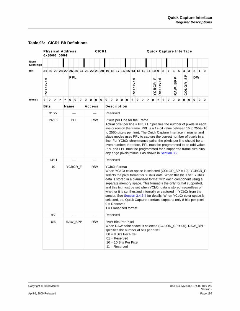
Quick Capture InterfaceRegister Descriptions
Copyright © 2009 Marvell Doc. No. MV-S301374-03 Rev. 2.0Version -
April 6, 2009 Released Page 199
12345678910111213141516171819202122232425262728293031323334353637383940414243444546474849505152535455565758
Table 96: CICR1 Bit Definitions
Physical Address0x5000_0004
CICR1 Quick Capture Interface
User Settings
Bit 31 30 29 28 27 26 25 24 23 22 21 20 19 18 17 16 15 14 13 12 11 10 9 8 7 6 5 4 3 2 1 0
Re
se
rve
d PPL
Re
se
rve
d
YC
BC
R_
F
Re
se
rve
d
RA
W_
BP
P
CO
LO
R_
SP DW
Reset ? ? ? ? ? 0 0 0 0 0 0 0 0 0 0 0 0 ? ? ? ? 0 ? ? ? 0 0 0 0 0 0 0
Bits Name Access Descript ion
31:27 — — Reserved
26:15 PPL R/W Pixels per Line for the FrameActual pixel per line = PPL+1. Specifies the number of pixels in each line or row on the frame. PPL is a 12-bit value between 15 to 2559 (16 to 2560 pixels per line). The Quick Capture Interface in master and slave modes uses PPL to capture the correct number of pixels in a line. For YCbCr chrominance pairs, the pixels per line should be an even number; therefore, PPL must be programmed to an odd value. PPL and LPF must be programmed for a supported frame size plus any edge pixels minus 1 as shown in Section 3.2.
14:11 — — Reserved
10 YCBCR_F R/W YCbCr FormatWhen YCbCr color space is selected (COLOR_SP = 10), YCBCR_F selects the pixel format for YCbCr data. When this bit is set, YCbCr data is stored in a planarized format with each component using a separate memory space. This format is the only format supported, and this bit must be set when YCbCr data is stored, regardless of whether it is synthesized internally or captured in YCbCr from the sensor. See Section 3.4.6.4 for details. When YCbCr color space is selected, the Quick Capture Interface supports only 8 bits per pixel.0 = Reserved1 = Planarized format
9:7 — — Reserved
6:5 RAW_BPP R/W RAW Bits Per PixelWhen RAW color space is selected (COLOR_SP = 00), RAW_BPP specifies the number of bits per pixel. 00 = 8 Bits Per Pixel 01 = Reserved 10 = 10 Bits Per Pixel 11 = Reserved
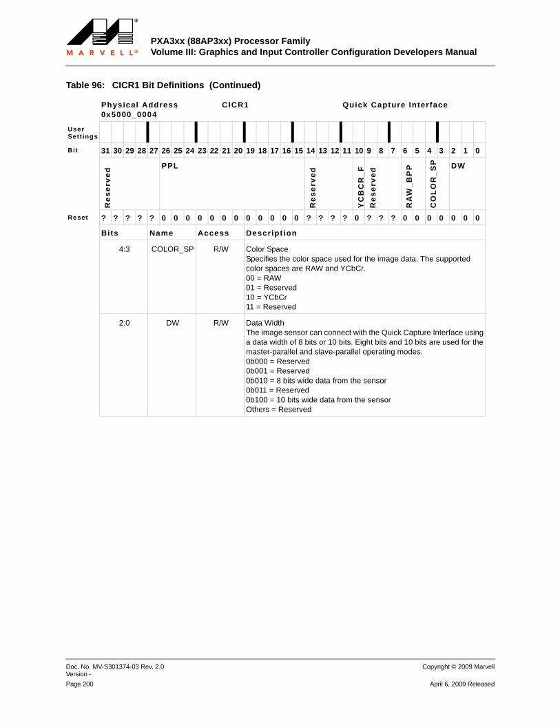
PXA3xx (88AP3xx) Processor FamilyVolume III: Graphics and Input Controller Configuration Developers Manual
Doc. No. MV-S301374-03 Rev. 2.0 Version -
Copyright © 2009 Marvell
Page 200 April 6, 2009 Released
12345678910111213141516171819202122232425262728293031323334353637383940414243444546474849505152535455565758
4:3 COLOR_SP R/W Color SpaceSpecifies the color space used for the image data. The supported color spaces are RAW and YCbCr.00 = RAW01 = Reserved 10 = YCbCr11 = Reserved
2:0 DW R/W Data WidthThe image sensor can connect with the Quick Capture Interface using a data width of 8 bits or 10 bits. Eight bits and 10 bits are used for the master-parallel and slave-parallel operating modes.0b000 = Reserved0b001 = Reserved0b010 = 8 bits wide data from the sensor0b011 = Reserved0b100 = 10 bits wide data from the sensorOthers = Reserved
Table 96: CICR1 Bit Definitions (Continued)
Physical Address0x5000_0004
CICR1 Quick Capture Interface
User Settings
Bit 31 30 29 28 27 26 25 24 23 22 21 20 19 18 17 16 15 14 13 12 11 10 9 8 7 6 5 4 3 2 1 0
Re
se
rve
d PPL
Re
se
rve
d
YC
BC
R_
F
Re
se
rve
d
RA
W_
BP
P
CO
LO
R_
SP DW
Reset ? ? ? ? ? 0 0 0 0 0 0 0 0 0 0 0 0 ? ? ? ? 0 ? ? ? 0 0 0 0 0 0 0
Bits Name Access Descript ion

Quick Capture InterfaceRegister Descriptions
Copyright © 2009 Marvell Doc. No. MV-S301374-03 Rev. 2.0Version -
April 6, 2009 Released Page 201
12345678910111213141516171819202122232425262728293031323334353637383940414243444546474849505152535455565758
3.5.4 Quick Capture Interface Control Register 2 (CICR2)CICR2, shown in Table 97, defines the wait counts at the beginning and end of a line, the width of horizontal sync signal, and the number of frames to skip at the beginning of a frame sequence. This is a read/write register. Ignore reads from reserved bits. Write 0b0 to reserved bits.
Table 97: CICR2 Bit Definitions
Physical Address0x5000_0008
CICR2 Quick Capture Interface
User Settings
Bit 31 30 29 28 27 26 25 24 23 22 21 20 19 18 17 16 15 14 13 12 11 10 9 8 7 6 5 4 3 2 1 0
BLW ELW HSW
Re
se
rve
d BFPW FSW
Reset 0 0 0 0 0 0 0 0 0 0 0 0 0 0 0 0 0 0 0 0 0 0 ? 0 0 0 0 0 0 0 0 0
Bits Name Access Description
31:24 BLW R/W Beginning-of-Line Pixel Clock Wait CountSpecifies the number of pixel clocks to wait from the active edge of CIF_HSYNC before starting the data capture. This wait count is used for both master and slave operating modes. BLW generates a wait period ranging from 0 to 255 pixel clock cycles.
23:16 ELW R/W End-of-Line Pixel Clock Wait CountSpecifies the number of pixel clocks to wait at the end of each line or row of pixels before pulsing CIF_HSYNC in Slave mode to begin the next line. This field is not used when the Quick Capture Interface operates in Master mode. The wait period after an end of line is guaranteed to be at least the number of clock cycles programmed into ELW + 1. Thus, a range of at least 1 to 256 pixel clock cycles is possible.
15:10 HSW R/W Horizontal Sync Pulse WidthValue (from3to 63). Specifies the pulse width of CIF_HSYNC in Slave mode. This field is not used when the Quick Capture Interface operates in Master mode. CIF_HSYNC is asserted each time the Quick Capture Interface begins to capture a line or row of pixels. HSW can be programmed to generate a CIF_HSYNC width ranging from 4 to 64 pixel clock periods. Program HSW with the required number of pixel clocks minus one. The polarity (active and inactive state) of the CIF_HSYNC pin is programmed using the horizontal sync polarity (HSP) bit in CICR4.
9 — — Reserved
8:3 BFPW R/W Beginning of Frame Pixel Clock Wait CountValue (from 0 to 63). Specifies the delay between the assertion of CIF_VSYNC and CIF_HSYNC in Slave mode. BFPW generates a delay ranging from 1 to 64 pixel clock cycles. Program BFPW with the preferred number of pixel clocks minus one.
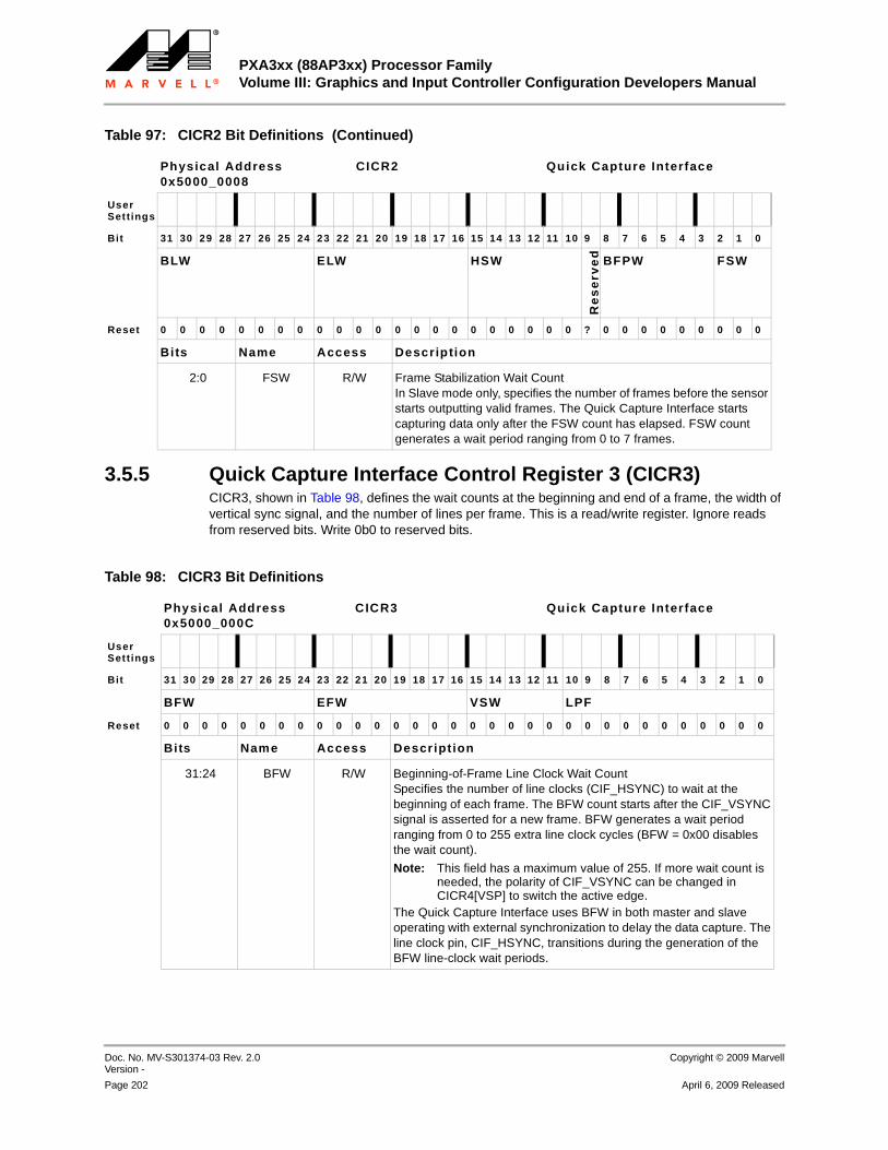
PXA3xx (88AP3xx) Processor FamilyVolume III: Graphics and Input Controller Configuration Developers Manual
Doc. No. MV-S301374-03 Rev. 2.0 Version -
Copyright © 2009 Marvell
Page 202 April 6, 2009 Released
12345678910111213141516171819202122232425262728293031323334353637383940414243444546474849505152535455565758
3.5.5 Quick Capture Interface Control Register 3 (CICR3)CICR3, shown in Table 98, defines the wait counts at the beginning and end of a frame, the width of vertical sync signal, and the number of lines per frame. This is a read/write register. Ignore reads from reserved bits. Write 0b0 to reserved bits.
2:0 FSW R/W Frame Stabilization Wait CountIn Slave mode only, specifies the number of frames before the sensor starts outputting valid frames. The Quick Capture Interface starts capturing data only after the FSW count has elapsed. FSW count generates a wait period ranging from 0 to 7 frames.
Table 97: CICR2 Bit Definitions (Continued)
Physical Address0x5000_0008
CICR2 Quick Capture Interface
User Settings
Bit 31 30 29 28 27 26 25 24 23 22 21 20 19 18 17 16 15 14 13 12 11 10 9 8 7 6 5 4 3 2 1 0
BLW ELW HSW
Re
se
rve
d BFPW FSW
Reset 0 0 0 0 0 0 0 0 0 0 0 0 0 0 0 0 0 0 0 0 0 0 ? 0 0 0 0 0 0 0 0 0
Bits Name Access Description
Table 98: CICR3 Bit Definitions
Physical Address0x5000_000C
CICR3 Quick Capture Interface
User Settings
Bit 31 30 29 28 27 26 25 24 23 22 21 20 19 18 17 16 15 14 13 12 11 10 9 8 7 6 5 4 3 2 1 0
BFW EFW VSW LPF
Reset 0 0 0 0 0 0 0 0 0 0 0 0 0 0 0 0 0 0 0 0 0 0 0 0 0 0 0 0 0 0 0 0
Bits Name Access Descript ion
31:24 BFW R/W Beginning-of-Frame Line Clock Wait CountSpecifies the number of line clocks (CIF_HSYNC) to wait at the beginning of each frame. The BFW count starts after the CIF_VSYNC signal is asserted for a new frame. BFW generates a wait period ranging from 0 to 255 extra line clock cycles (BFW = 0x00 disables the wait count).
Note: This field has a maximum value of 255. If more wait count is needed, the polarity of CIF_VSYNC can be changed in CICR4[VSP] to switch the active edge.
The Quick Capture Interface uses BFW in both master and slave operating with external synchronization to delay the data capture. The line clock pin, CIF_HSYNC, transitions during the generation of the BFW line-clock wait periods.

Quick Capture InterfaceRegister Descriptions
Copyright © 2009 Marvell Doc. No. MV-S301374-03 Rev. 2.0Version -
April 6, 2009 Released Page 203
12345678910111213141516171819202122232425262728293031323334353637383940414243444546474849505152535455565758
23:16 EFW R/W End-of-Frame Line Clock Wait CountSpecifies the number of line clocks (CIF_HSYNC) to wait at the end of each frame when the Quick Capture Interface operates in Slave mode. When the Quick Capture Interface captures a complete frame of pixels (as indicated by pixels-per-line and lines-per-frame counters), the value in EFW counts the number of line clock periods to wait. After the count elapses, the CIF_VSYNC signal is pulsed to start the next frame capture. EFW generates a wait period ranging from 0 to 255 line clock cycles (CIF_VSYNC pulse width = (VSW+1)). Clearing EFW disables the EOF wait count. The line clock pin, CIF_HSYNC, does not transition during the generation of the EFW line clock periods. EFW count is not used in Master mode.
15:11 VSW R/W Vertical Sync Pulse WidthSpecifies the width of CIF_VSYNC in Slave mode. This field is not used in Master mode. CIF_VSYNC is asserted each time the Quick Capture Interface begins to capture a frame. VSW can be programmed to generate a CIF_VSYNC width ranging from one to 32 pixel clock periods. Program VSW with the required number of pixel clocks minus one. The polarity (active and inactive state) of the CIF_VSYNC pin is programmed using the vertical-sync polarity (VSP) bit in CICR4.
10:0 LPF R/W Lines per FrameValue (from 15 to 2047). Specifies the number of lines in one frame of data. The Quick Capture Interface in master and Slave mode uses LPF to determine the end-of-frame capture. Program PPL and LPF for an accepted frame size as shown in Section 3.2.
Table 98: CICR3 Bit Definitions (Continued)
Physical Address0x5000_000C
CICR3 Quick Capture Interface
User Settings
Bit 31 30 29 28 27 26 25 24 23 22 21 20 19 18 17 16 15 14 13 12 11 10 9 8 7 6 5 4 3 2 1 0
BFW EFW VSW LPF
Reset 0 0 0 0 0 0 0 0 0 0 0 0 0 0 0 0 0 0 0 0 0 0 0 0 0 0 0 0 0 0 0 0
Bits Name Access Descript ion

PXA3xx (88AP3xx) Processor FamilyVolume III: Graphics and Input Controller Configuration Developers Manual
Doc. No. MV-S301374-03 Rev. 2.0 Version -
Copyright © 2009 Marvell
Page 204 April 6, 2009 Released
12345678910111213141516171819202122232425262728293031323334353637383940414243444546474849505152535455565758
3.5.6 Quick Capture Interface Control Register 4 (CICR4)CICR4, shown in Table 99, contains fields to control various functions of the Quick Capture Interface. The interface must be disabled (ENB cleared) when the state of any field within this register is changed. This is a read/write register. Ignore reads from reserved bits. Write 0b0 to reserved bits.
Table 99: CICR4 Bit Definitions
Physical Address0x5000_0010
CICR4 Quick Capture Interface
User Settings
Bit 31 30 29 28 27 26 25 24 23 22 21 20 19 18 17 16 15 14 13 12 11 10 9 8 7 6 5 4 3 2 1 0
PX
A3
2x
an
dP
XA
30
x O
nly Reserved
PC
LK
_E
N
PC
P
HS
P
VS
P
MC
LK
_E
N Reserved
FR
_R
AT
E D IV
PX
A3
1x
On
ly
Re
se
rve
d
YC
BC
R_
DS
Re
se
rve
d
PC
LK
_E
N
PC
P
HS
P
VS
P
MC
LK
_E
N Reserved
FR
_R
AT
E
D IV
Reset ? ? ? ? 0 ? ? ? 0 0 0 0 0 ? ? ? ? ? ? ? ? 0 0 0 0 0 0 0 0 0 0 0
Bits Name Access Description
31:28 — — Reserved
27
— — Reserved (PXA32x and PXA30x Only)
YCBCR_DS R/W YCbCr Down Sample (YCBCR_DS)Enables the output of YCbCr 4:2:0 data from the camera interface.YCBCR 4:2:2 → 4:2:0 enable0 = No conversion1 = Enable conversionNOTE: PXA31x Only
26:24 — — Reserved
23 PCLK_EN R/W Pixel Clock EnableSpecifies whether the sensor supplies a pixel clock to the Quick Capture Interface. When it does not, PCLK_EN must be cleared and the Quick Capture Interface uses CIF_MCLK to clock pixel data. Set this bit if the sensor supplies a pixel clock along with pixel data. 0 = The sensor does not supply CIF_PCLK.1 = The sensor supplies CIF_PCLK.
22 PCP R/W Pixel Clock PolaritySelects which edge of the pixel clock data is sampled on the CIF_DD data pins. When CICR4[PCLK_EN] is clear and CICR4[MCLK_EN] is set, PCP selects the active edge of CIF_MCLK.0 = Data is sampled on the rising edge of CIF_PCLK.1 = Data is sampled on the falling edge of CIF_PCLK.

Quick Capture InterfaceRegister Descriptions
Copyright © 2009 Marvell Doc. No. MV-S301374-03 Rev. 2.0Version -
April 6, 2009 Released Page 205
12345678910111213141516171819202122232425262728293031323334353637383940414243444546474849505152535455565758
21 HSP R/W Horizontal Sync Polarity Selects the active and inactive states of the horizontal sync CIF_HSYNC signal. This polarity control applies in both master and slave operating modes.0 = CIF_HSYNC is active high and inactive low.1 = CIF_HSYNC is active low and inactive high.
20 VSP R/W Vertical Sync PolaritySelects the active and inactive states of the vertical sync signal (CIF_VSYNC). This polarity control applies in both master and slave operating modes.0 = CIF_VSYNC is active high and inactive low.1 = CIF_VSYNC is active low and inactive high.
19 MCLK_EN R/W MCLK EnableThe clock enable for CIF_MCLK, which the Quick Capture Interface supplies to the sensor. Set MCLK_EN to supply the clock at the rate specified by CICR4[DIV]. Turn off CIF_MCLK by clearing MCLK_EN.
Note: Clearing both MCLK_EN and PCLK_EN in CICR4 is a non-valid clock configuration, and the Quick Capture Interface captures no data.
0 = Quick Capture Interface does not supply CIF_MCLK to the sensor.1 = Quick Capture Interface supplies CIF_MCLK to the sensor.
18:11 — — Reserved
Table 99: CICR4 Bit Definitions (Continued)
Physical Address0x5000_0010
CICR4 Quick Capture Interface
User Settings
Bit 31 30 29 28 27 26 25 24 23 22 21 20 19 18 17 16 15 14 13 12 11 10 9 8 7 6 5 4 3 2 1 0
PX
A3
2x
an
dP
XA
30
x O
nly Reserved
PC
LK
_E
N
PC
P
HS
P
VS
P
MC
LK
_E
N Reserved
FR
_R
AT
E D IV
PX
A3
1x
On
ly
Re
se
rve
d
YC
BC
R_
DS
Re
se
rve
d
PC
LK
_E
N
PC
P
HS
P
VS
P
MC
LK
_E
N Reserved
FR
_R
AT
E
D IV
Reset ? ? ? ? 0 ? ? ? 0 0 0 0 0 ? ? ? ? ? ? ? ? 0 0 0 0 0 0 0 0 0 0 0
Bits Name Access Description

PXA3xx (88AP3xx) Processor FamilyVolume III: Graphics and Input Controller Configuration Developers Manual
Doc. No. MV-S301374-03 Rev. 2.0 Version -
Copyright © 2009 Marvell
Page 206 April 6, 2009 Released
12345678910111213141516171819202122232425262728293031323334353637383940414243444546474849505152535455565758
3.5.7 Quick Capture Interface Timeout Register (CITOR)CITOR, shown in Table 100, contains the timeout value to specify the period of inactivity in the Quick Capture Interface FIFOs. This is a read/write register. Ignore reads from reserved bits. Write 0b0 to reserved bits.
10:8 FR_RATE R/W Frame Capture RateSpecifies the rate at which the Quick Capture Interface captures the incoming frames. You can program this field to capture frames at a rate lower than the sensor output rate. The capture rate values are as follows:000 = All incoming frames001 = 1 out of every 2 frames010 = 1 out of every 3 frames011 = 1 out of every 4 frames100 = 1 out of every 5 frames101 = 1 out of every 6 frames110 = 1 out of every 7 frames111 = 1 out of every 8 frames
7:0 DIV R/W Clock DivisorSelects the frequency of the master clock (CIF_MCLK) supplied to the image sensor. DIV can be of any value from 10 to 255 and is used to generate a range of CIF_MCLK frequencies from CICLK/24 to CICLK/512, where CICLK is the clock input of the Quick Capture Interface:
Table 99: CICR4 Bit Definitions (Continued)
Physical Address0x5000_0010
CICR4 Quick Capture Interface
User Settings
Bit 31 30 29 28 27 26 25 24 23 22 21 20 19 18 17 16 15 14 13 12 11 10 9 8 7 6 5 4 3 2 1 0
PX
A3
2x
an
dP
XA
30
x O
nly Reserved
PC
LK
_E
N
PC
P
HS
P
VS
P
MC
LK
_E
N Reserved
FR
_R
AT
E D IV
PX
A3
1x
On
ly
Re
se
rve
d
YC
BC
R_
DS
Re
se
rve
d
PC
LK
_E
N
PC
P
HS
P
VS
P
MC
LK
_E
N Reserved
FR
_R
AT
E
D IV
Reset ? ? ? ? 0 ? ? ? 0 0 0 0 0 ? ? ? ? ? ? ? ? 0 0 0 0 0 0 0 0 0 0 0
Bits Name Access Description
MCLKCICLK
2 DIV 1+( )----------------------------=
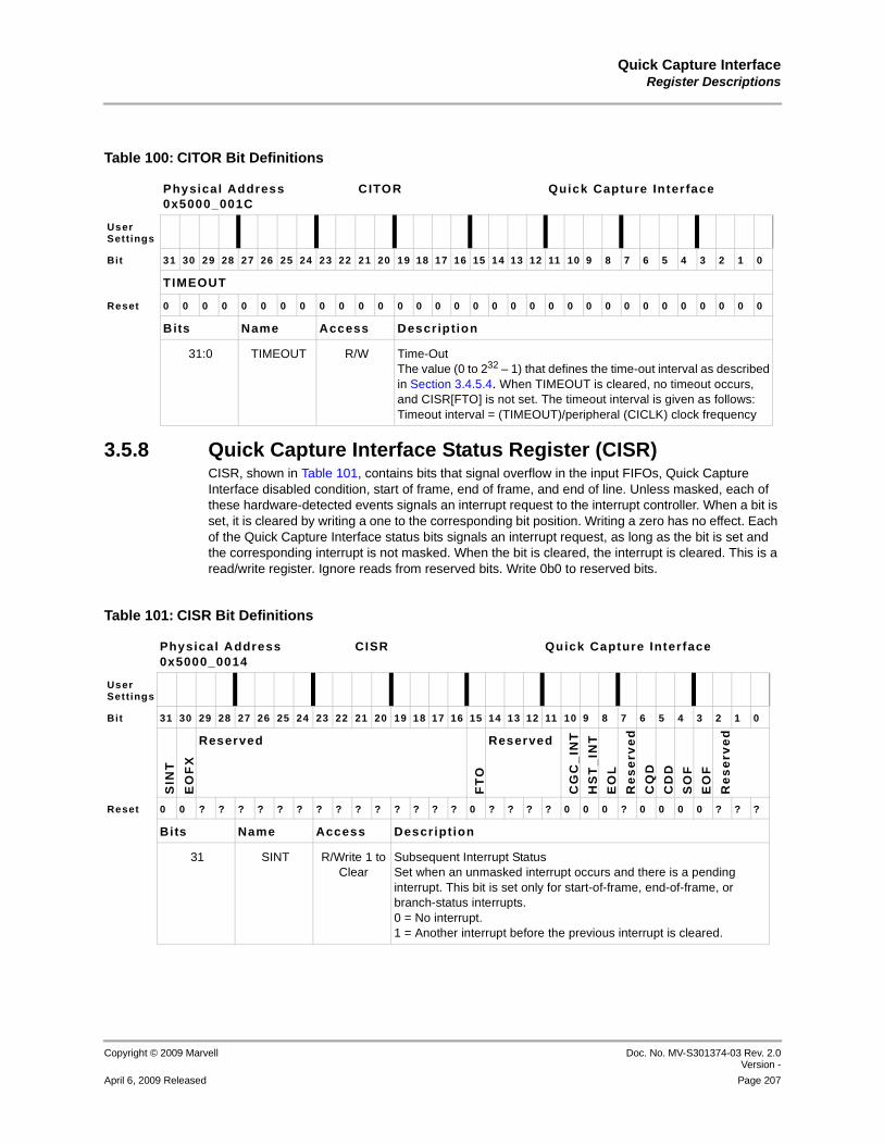
Quick Capture InterfaceRegister Descriptions
Copyright © 2009 Marvell Doc. No. MV-S301374-03 Rev. 2.0Version -
April 6, 2009 Released Page 207
12345678910111213141516171819202122232425262728293031323334353637383940414243444546474849505152535455565758
3.5.8 Quick Capture Interface Status Register (CISR)CISR, shown in Table 101, contains bits that signal overflow in the input FIFOs, Quick Capture Interface disabled condition, start of frame, end of frame, and end of line. Unless masked, each of these hardware-detected events signals an interrupt request to the interrupt controller. When a bit is set, it is cleared by writing a one to the corresponding bit position. Writing a zero has no effect. Each of the Quick Capture Interface status bits signals an interrupt request, as long as the bit is set and the corresponding interrupt is not masked. When the bit is cleared, the interrupt is cleared. This is a read/write register. Ignore reads from reserved bits. Write 0b0 to reserved bits.
Table 100: CITOR Bit Definitions
Physical Address0x5000_001C
CITOR Quick Capture Inter face
User Settings
Bit 31 30 29 28 27 26 25 24 23 22 21 20 19 18 17 16 15 14 13 12 11 10 9 8 7 6 5 4 3 2 1 0
TIMEOUT
Reset 0 0 0 0 0 0 0 0 0 0 0 0 0 0 0 0 0 0 0 0 0 0 0 0 0 0 0 0 0 0 0 0
Bits Name Access Description
31:0 TIMEOUT R/W Time-OutThe value (0 to 232 – 1) that defines the time-out interval as described in Section 3.4.5.4. When TIMEOUT is cleared, no timeout occurs, and CISR[FTO] is not set. The timeout interval is given as follows: Timeout interval = (TIMEOUT)/peripheral (CICLK) clock frequency
Table 101: CISR Bit Definitions
Physical Address0x5000_0014
CISR Quick Capture Interface
User Settings
Bit 31 30 29 28 27 26 25 24 23 22 21 20 19 18 17 16 15 14 13 12 11 10 9 8 7 6 5 4 3 2 1 0
SIN
T
EO
FX
Reserved
FT
O
Reserved
CG
C_
INT
HS
T_
INT
EO
L
Re
se
rve
d
CQ
D
CD
D
SO
F
EO
F
Re
se
rve
d
Reset 0 0 ? ? ? ? ? ? ? ? ? ? ? ? ? ? 0 ? ? ? ? 0 0 0 ? 0 0 0 0 ? ? ?
Bits Name Access Descript ion
31 SINT R/Write 1 to Clear
Subsequent Interrupt StatusSet when an unmasked interrupt occurs and there is a pending interrupt. This bit is set only for start-of-frame, end-of-frame, or branch-status interrupts.0 = No interrupt.1 = Another interrupt before the previous interrupt is cleared.

PXA3xx (88AP3xx) Processor FamilyVolume III: Graphics and Input Controller Configuration Developers Manual
Doc. No. MV-S301374-03 Rev. 2.0 Version -
Copyright © 2009 Marvell
Page 208 April 6, 2009 Released
12345678910111213141516171819202122232425262728293031323334353637383940414243444546474849505152535455565758
30 EOFX R/Write 1 to Clear
End-of-Frame Transferred to Memory (Channel 0-2, not Channel 3)Set when a complete image frame is transferred to memory. This interrupt enables the graphic/LCD controller for rotation of the image frame stored to memory. For GCU handshaking, the GCU executes a store reg instruction (writing a 1) when it is ready for the next frame. For LCD handshaking, software clears this interrupt. To mask this interrupt, set the corresponding mask bit by clearing CICR0[EOFXM]. 0 = Memory has not received an end-of-frame.1 = Memory has received an end-of-frame.
29:16 — — Reserved
15 FTO R/Write 1 to Clear
FIFO Time-outSet when the Quick Capture Interface FIFO is idle (no samples received) for a period of time defined by the value programmed within the timeout register (CITOR). To mask this interrupt, set the corresponding mask bit by clearing CICR0[TOM].0 = FIFO time-out has not occurred.1 = FIFO time-out has occurred.
14:11 — — Reserved
10 CGC_INT R/Write 1 to Clear
Compander InterruptSet when the compander RAM is not loaded and CGC is enabled (CICCR[EN]).0 = Either CGC RAM has been loaded or CGC is disabled.1 = CGC RAM was not loaded before enabling CGC (CICCR[EN]).
9 HST_INT R/Write 1 to Clear
Histogram InterruptSet when the histogram RAM is cleared of all statistical data and is ready to capture new statistical data for a new frame (HST_INT = 1).0 = HST RAM not cleared.1 = HST RAM is cleared.
8 EOL R/Write 1 to Clear
End of LineSet when the Quick Capture Interface finishes capturing all pixels in a line. When EOL is set, an interrupt request is sent to the interrupt controller if it is unmasked (EOLM cleared).0 = Quick Capture Interface has not received an end-of-line.1 = Quick Capture Interface has received an end-of-line.
7 — — Reserved
Table 101: CISR Bit Definitions (Continued)
Physical Address0x5000_0014
CISR Quick Capture Interface
User Settings
Bit 31 30 29 28 27 26 25 24 23 22 21 20 19 18 17 16 15 14 13 12 11 10 9 8 7 6 5 4 3 2 1 0
SIN
T
EO
FX
Reserved
FT
O
Reserved
CG
C_
INT
HS
T_
INT
EO
L
Re
se
rve
d
CQ
D
CD
D
SO
F
EO
F
Re
se
rve
d
Reset 0 0 ? ? ? ? ? ? ? ? ? ? ? ? ? ? 0 ? ? ? ? 0 0 0 ? 0 0 0 0 ? ? ?
Bits Name Access Descript ion

Quick Capture InterfaceRegister Descriptions
Copyright © 2009 Marvell Doc. No. MV-S301374-03 Rev. 2.0Version -
April 6, 2009 Released Page 209
12345678910111213141516171819202122232425262728293031323334353637383940414243444546474849505152535455565758
6 CQD R/Write 1 to Clear
Quick Capture Interface Quick Disable StatusSet when the Quick Capture Interface enable (ENB) bit is cleared. When CQD is set, an interrupt request is made to the interrupt controller if the CQD interrupt is unmasked (CICR0[QDM] cleared). If set, CQD forces the interface to stop capturing data and quit driving the Quick Capture Interface pins. This method of disable is for use with sleep/deep-sleep shutdown. When CQD is set, the core can access the Quick Capture Interface control and status registers. Monitor the CQD interrupt before placing the processor into sleep or deep-sleep modes to ensure that the interface is disabled. 0 = No quick disable.1 = The Quick Capture Interface has been quickly disabled.
5 CDD R/Write 1 to Clear
Quick Capture Interface Disable DoneSet after the Quick Capture Interface is disabled and the frame is captured. When the Quick Capture Interface is disabled by setting the Quick Capture Interface disable bit (CICR0[DIS]), the interface allows the current frame capture to complete before it is disabled. After the last set of pixels is read from the FIFO, the interface stops data capture, CDD is set, and an interrupt request is sent to the interrupt controller if it is unmasked (CDM is cleared). A set CDD implies that the interface has stopped capturing data and Quick Capture Interface pins are no longer driven. When CDD is set, the core can access the Quick Capture Interface control and status registers. The Quick Capture Interface disable-done interrupt is useful to allow an orderly shutdown of the Quick Capture Interface before the processor is placed into S2/D3/C4 or S3/D4/C4 low-power states.0 = Quick Capture Interface not disabled.1 = Quick Capture Interface disabled and the active frame has
completed.
4 SOF R/Write 1 to Clear
Start-of-FrameSet when the Quick Capture Interface detects the start of a frame. When SOF is set, an interrupt request is sent to the interrupt controller if it is unmasked (CICR0[SOFM] cleared).0 = Quick Capture Interface has not received a start-of-frame.1 = Quick Capture Interface has received a start-of-frame.
Table 101: CISR Bit Definitions (Continued)
Physical Address0x5000_0014
CISR Quick Capture Interface
User Settings
Bit 31 30 29 28 27 26 25 24 23 22 21 20 19 18 17 16 15 14 13 12 11 10 9 8 7 6 5 4 3 2 1 0
SIN
T
EO
FX
Reserved
FT
O
Reserved
CG
C_
INT
HS
T_
INT
EO
L
Re
se
rve
d
CQ
D
CD
D
SO
F
EO
F
Re
se
rve
d
Reset 0 0 ? ? ? ? ? ? ? ? ? ? ? ? ? ? 0 ? ? ? ? 0 0 0 ? 0 0 0 0 ? ? ?
Bits Name Access Descript ion

PXA3xx (88AP3xx) Processor FamilyVolume III: Graphics and Input Controller Configuration Developers Manual
Doc. No. MV-S301374-03 Rev. 2.0 Version -
Copyright © 2009 Marvell
Page 210 April 6, 2009 Released
12345678910111213141516171819202122232425262728293031323334353637383940414243444546474849505152535455565758
3.5.9 Quick Capture Interface Return Clock Delay Register (CIRCD)CIRCD, shown in Table 102, holds the delay selects to delay either CIF_PCLK/returned CIF_MCLK.
3 EOF R/Write 1 to Clear
End-of-FrameSet when the Quick Capture Interface finishes capturing all the lines in a frame. When EOF is set, an interrupt request is sent to the interrupt controller if it is unmasked (EOFM cleared).
Note: This bit only identifies that the EOF is captured. It does not indicate that the frame data has been transferred to memory. The EOFX signal must be used to identify when a complete frame is transferred to memory.
0 = Quick Capture Interface has not received an end-of-frame.1 = Quick Capture Interface has received an end-of-frame.
2:0 — — Reserved
Table 101: CISR Bit Definitions (Continued)
Physical Address0x5000_0014
CISR Quick Capture Interface
User Settings
Bit 31 30 29 28 27 26 25 24 23 22 21 20 19 18 17 16 15 14 13 12 11 10 9 8 7 6 5 4 3 2 1 0
SIN
T
EO
FX
Reserved
FT
O
Reserved
CG
C_
INT
HS
T_
INT
EO
L
Re
se
rve
d
CQ
D
CD
D
SO
F
EO
F
Re
se
rve
d
Reset 0 0 ? ? ? ? ? ? ? ? ? ? ? ? ? ? 0 ? ? ? ? 0 0 0 ? 0 0 0 0 ? ? ?
Bits Name Access Descript ion

Quick Capture InterfaceRegister Descriptions
Copyright © 2009 Marvell Doc. No. MV-S301374-03 Rev. 2.0Version -
April 6, 2009 Released Page 211
12345678910111213141516171819202122232425262728293031323334353637383940414243444546474849505152535455565758
Table 102: CIRCD Bit Definitions
Physical Address0x5000_0044
CIRCD Quick Capture Interface
User Settings
Bit 31 30 29 28 27 26 25 24 23 22 21 20 19 18 17 16 15 14 13 12 11 10 9 8 7 6 5 4 3 2 1 0
CL
K_
SE
L
FV
_S
EL
LV
_S
EL
DA
TA
_S
EL
DL
YC
EL
L_
SE
L
CE
LL
1_
DL
Y
CE
LL
2_
DL
Y
CE
LL
3_
DL
Y
CE
LL
4_
DL
Y
CE
LL
5_
DL
Y
CE
LL
6_
DL
Y
CE
LL
7_
DL
Y
CE
LL
8_
DL
Y
Reset 0 0 0 0 0 0 0 0 0 0 0 0 0 0 0 0 0 0 0 0 0 0 0 0 0 0 0 0 0 0 0 0
Bits Name Access Descript ion
31 CLK_SEL R/W Clock SelectSelects the clock from either the return clock module or non-return clock path. The default is the return clock path, which must be used for Slave mode. For Master mode, the clock could be selected from the non-return clock path.0 = Clock from return clock path1 = Clock from non return clock path
30 FV_SEL R/W Frame Valid SelectSelects the frame valid from either the return clock module or non-return clock path. The default is the return clock path, which must be used for Slave mode. For Master mode, frame valid can be selected from the non-return clock path0 = Vertical Sync from return clock path1 = Vertical Sync from non return clock path
29 LV_SEL R/W Line Valid SelectSelects the line valid from either the return clock module or non-return clock path. The default is the return clock path, which must be used for Slave mode. For Master mode, line valid could be selected from the non-return clock path.0 = Horizontal Sync from return clock path1 = Horizontal Sync from non return clock path
28 DATA_SEL R/W Data SelectSelects the data from either the return clock module or non-return clock path. 0 = Data from return clock path1 = Data from non return clock path

PXA3xx (88AP3xx) Processor FamilyVolume III: Graphics and Input Controller Configuration Developers Manual
Doc. No. MV-S301374-03 Rev. 2.0 Version -
Copyright © 2009 Marvell
Page 212 April 6, 2009 Released
12345678910111213141516171819202122232425262728293031323334353637383940414243444546474849505152535455565758
27:24 DLYCELL_SEL
R/W Delay Cell SelectSelects the output of one of the eight programmable delay elements. This field applies only when the inputs are chosen from the return clock path. 0b0000 = No delay0b0001 = Delay cell 1 output0b0010 = Delay cell 2 output0b0011= Delay cell 3 output0b0100 = Delay cell 4 output0b0101 = Delay cell 5 output0b0110 = Delay cell 6 output0b1000 = Delay cell 7 output0b1001 = Delay cell 8 outputOthers = Reserved
CELLx_DLY: Used to program the delay on the delay elements. These delays range from approximately 1.6 ns to 3.0 ns:
23:21 CELL1_DLY R/W Controls the delay on cell 1
20:18 CELL2_DLY R/W Controls the delay on cell 2
17:15 CELL3_DLY R/W Controls the delay on cell 3
14:12 CELL4_DLY R/W Controls the delay on cell 4
11:9 CELL5_DLY R/W Controls the delay on cell 5
8:6 CELL6_DLY R/W Controls the delay on cell 6
5:3 CELL7_DLY R/W Controls the delay on cell 7
2:0 CELL8_DLY R/W Controls the delay on cell 8
Table 102: CIRCD Bit Definitions (Continued)
Physical Address0x5000_0044
CIRCD Quick Capture Interface
User Settings
Bit 31 30 29 28 27 26 25 24 23 22 21 20 19 18 17 16 15 14 13 12 11 10 9 8 7 6 5 4 3 2 1 0
CL
K_
SE
L
FV
_S
EL
LV
_S
EL
DA
TA
_S
EL
DL
YC
EL
L_
SE
L
CE
LL
1_
DL
Y
CE
LL
2_
DL
Y
CE
LL
3_
DL
Y
CE
LL
4_
DL
Y
CE
LL
5_
DL
Y
CE
LL
6_
DL
Y
CE
LL
7_
DL
Y
CE
LL
8_
DL
Y
Reset 0 0 0 0 0 0 0 0 0 0 0 0 0 0 0 0 0 0 0 0 0 0 0 0 0 0 0 0 0 0 0 0
Bits Name Access Descript ion

Quick Capture InterfaceRegister Descriptions
Copyright © 2009 Marvell Doc. No. MV-S301374-03 Rev. 2.0Version -
April 6, 2009 Released Page 213
12345678910111213141516171819202122232425262728293031323334353637383940414243444546474849505152535455565758
3.5.10 Quick Capture JPEG Control and Status Register (CIJPEG)CIJPEG, shown in Table 103, contains all bit fields related to the JPEG capture feature of the Quick Capture Interface.
Note
Note PXA31x processor only.
3.5.11 Quick Capture Interface Receive Buffer Register 0 (CIBR0)CIBR0, shown in Table 104, holds the data word to which the Read pointer in the Channel 0 FIFO points. Eight bytes (7–0) of the Channel 0 FIFO entry are read from the CIBR0 location before the Read pointer is incremented to point to the next FIFO entry. This is a read-only register. Ignore reads from reserved bits.
Table 103: CIJPEG Bit Definitions
Physical Address0x5000_0048
CIJPEG Quick Capture Interface
User Settings
Bit 31 30 29 28 27 26 25 24 23 22 21 20 19 18 17 16 15 14 13 12 11 10 9 8 7 6 5 4 3 2 1 0
Reserved
JP
EG
_E
RR
JP
EG
_E
N BYTE_CNT
Reset ? ? ? ? ? ? 0 0 0 0 0 0 0 0 0 0 0 0 0 0 0 0 0 0 0 0 0 0 0 0 0 0
Bits Name Access Descript ion
31:26 — — Reserved
25 JPEG_ERR R/W JPEG Capture ErrorSet when the HSYNC signal is high and the VSYNC signal is low.0 = No error1 = Error detected at the end of the capture operation
24 JPEG_EN R/W JPEG EnableEnables JPEG mode. The PPL and LPF counts are ignored so the CI controller captures data based on the VSYNC and HSYNC signals.0 = Normal operation1 = JPEG mode
23:0 BYTE_CNT R/W JPEG Captured Pixel CountContains the current number of bytes captured by the interface controller, which is equal to the number of pixel clock cycles HSYNC is high in JPEG mode. After the contents of this field are read at the end of a frame, software can clear this field.The present number of bytes captured in JPEG mode

PXA3xx (88AP3xx) Processor FamilyVolume III: Graphics and Input Controller Configuration Developers Manual
Doc. No. MV-S301374-03 Rev. 2.0 Version -
Copyright © 2009 Marvell
Page 214 April 6, 2009 Released
12345678910111213141516171819202122232425262728293031323334353637383940414243444546474849505152535455565758
3.5.12 Quick Capture Interface Receive Buffer Register 1 (CIBR1)CIBR1, shown in Table 105, holds the data word to which the Read pointer in the Channel 1 FIFO points. Eight bytes (7–0) of the Channel 1 FIFO entry are read from the CIBR1 location before the Read pointer is incremented to point to the next FIFO entry. This is a read-only register. Ignore reads from reserved bits.
3.5.13 Quick Capture Interface Receive Buffer Register 2 (CIBR2)CIBR2, shown in Table 106, holds the data word to which the Read pointer in the Channel 2 FIFO points. Eight bytes (7–0) of the Channel 2 FIFO entry are read from the CIBR2 location before the Read pointer is incremented to point to the next FIFO entry. This is a read-only register. Ignore reads from reserved bits.
Table 104: CIBR0 Bit Definitions
Physical Address0x5000_0028
CIBR0 Quick Capture Interface
User Settings
Bit 31 30 29 28 27 26 25 24 23 22 21 20 19 18 17 16 15 14 13 12 11 10 9 8 7 6 5 4 3 2 1 0
Byte 3 Byte 2 Byte 1 Byte 0
Reset 0 0 0 0 0 0 0 0 0 0 0 0 0 0 0 0 0 0 0 0 0 0 0 0 0 0 0 0 0 0 0 0
Bits Name Access Description
31:24 Byte 3 R Byte 3 of the Captured data in Channel 0
23:16 Byte 2 R Byte 2 of the Captured data in Channel 0
15:8 Byte 1 R Byte 1 of the Captured data in Channel 0
7:0 Byte 0 R Byte 0 of the Captured data in Channel 0
Table 105: CIBR1 Bit Definitions
Physical Address0x5000_0030
CIBR1 Quick Capture Interface
User Settings
Bit 31 30 29 28 27 26 25 24 23 22 21 20 19 18 17 16 15 14 13 12 11 10 9 8 7 6 5 4 3 2 1 0
Byte 3 Byte 2 Byte 1 Byte 0
Reset 0 0 0 0 0 0 0 0 0 0 0 0 0 0 0 0 0 0 0 0 0 0 0 0 0 0 0 0 0 0 0 0
Bits Name Access Descript ion
31:24 Byte 3 R Byte 3 of the Captured data in Channel 1
23:16 Byte 2 R Byte 2 of the Captured data in Channel 1
15:8 Byte 1 R Byte 1 of the Captured data in Channel 1
7:0 Byte 0 R Byte 0 of the Captured data in Channel 1
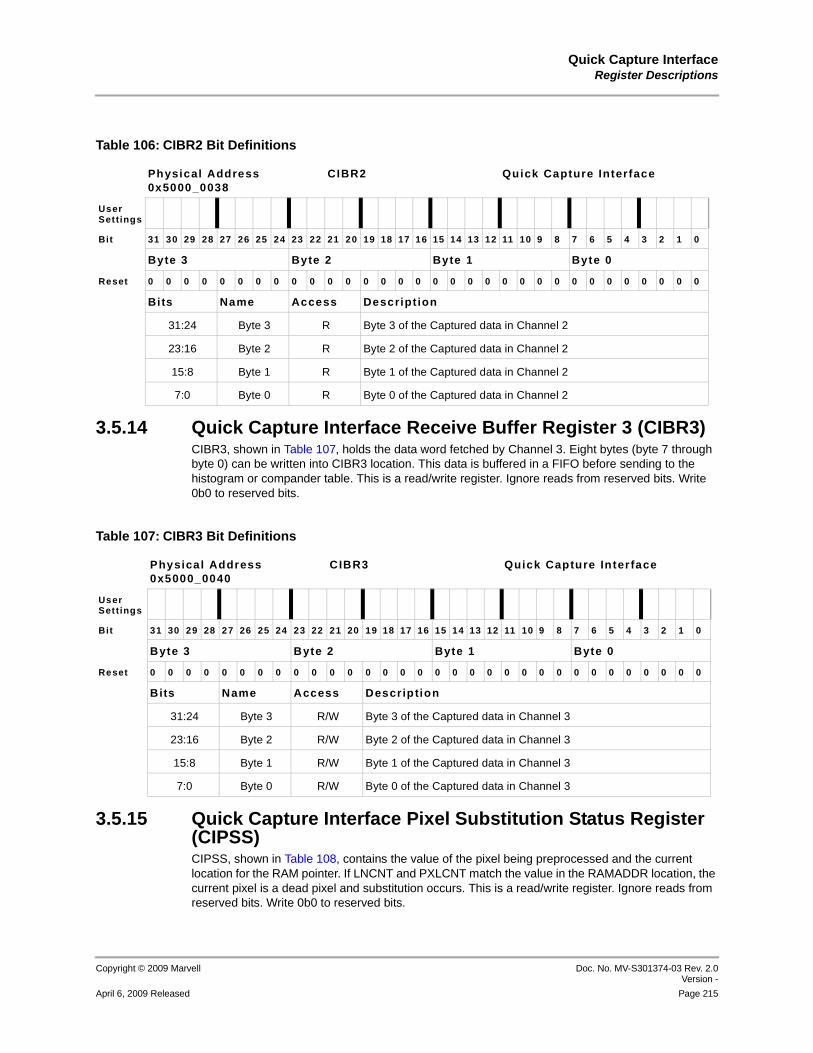
Quick Capture InterfaceRegister Descriptions
Copyright © 2009 Marvell Doc. No. MV-S301374-03 Rev. 2.0Version -
April 6, 2009 Released Page 215
12345678910111213141516171819202122232425262728293031323334353637383940414243444546474849505152535455565758
3.5.14 Quick Capture Interface Receive Buffer Register 3 (CIBR3)CIBR3, shown in Table 107, holds the data word fetched by Channel 3. Eight bytes (byte 7 through byte 0) can be written into CIBR3 location. This data is buffered in a FIFO before sending to the histogram or compander table. This is a read/write register. Ignore reads from reserved bits. Write 0b0 to reserved bits.
3.5.15 Quick Capture Interface Pixel Substitution Status Register (CIPSS)CIPSS, shown in Table 108, contains the value of the pixel being preprocessed and the current location for the RAM pointer. If LNCNT and PXLCNT match the value in the RAMADDR location, the current pixel is a dead pixel and substitution occurs. This is a read/write register. Ignore reads from reserved bits. Write 0b0 to reserved bits.
Table 106: CIBR2 Bit Definitions
Physical Address0x5000_0038
CIBR2 Quick Capture Interface
User Settings
Bit 31 30 29 28 27 26 25 24 23 22 21 20 19 18 17 16 15 14 13 12 11 10 9 8 7 6 5 4 3 2 1 0
Byte 3 Byte 2 Byte 1 Byte 0
Reset 0 0 0 0 0 0 0 0 0 0 0 0 0 0 0 0 0 0 0 0 0 0 0 0 0 0 0 0 0 0 0 0
Bits Name Access Descript ion
31:24 Byte 3 R Byte 3 of the Captured data in Channel 2
23:16 Byte 2 R Byte 2 of the Captured data in Channel 2
15:8 Byte 1 R Byte 1 of the Captured data in Channel 2
7:0 Byte 0 R Byte 0 of the Captured data in Channel 2
Table 107: CIBR3 Bit Definitions
Physical Address0x5000_0040
CIBR3 Quick Capture Inter face
User Settings
Bit 31 30 29 28 27 26 25 24 23 22 21 20 19 18 17 16 15 14 13 12 11 10 9 8 7 6 5 4 3 2 1 0
Byte 3 Byte 2 Byte 1 Byte 0
Reset 0 0 0 0 0 0 0 0 0 0 0 0 0 0 0 0 0 0 0 0 0 0 0 0 0 0 0 0 0 0 0 0
Bits Name Access Description
31:24 Byte 3 R/W Byte 3 of the Captured data in Channel 3
23:16 Byte 2 R/W Byte 2 of the Captured data in Channel 3
15:8 Byte 1 R/W Byte 1 of the Captured data in Channel 3
7:0 Byte 0 R/W Byte 0 of the Captured data in Channel 3

PXA3xx (88AP3xx) Processor FamilyVolume III: Graphics and Input Controller Configuration Developers Manual
Doc. No. MV-S301374-03 Rev. 2.0 Version -
Copyright © 2009 Marvell
Page 216 April 6, 2009 Released
12345678910111213141516171819202122232425262728293031323334353637383940414243444546474849505152535455565758
3.5.16 Quick Capture Interface Pixel Substitution Buffer (CIPBUF)CIPBUF, shown in Table 109, contains the description of the dead pixel location to store into the next location of the RAM. Do not enable the PSU until after the RAM is filled with all the dead pixel addresses. If there are not 128 dead pixels, fill the last location with 0x0000_0000, signifying the end of the dead pixel addresses stored in the RAM. Each Write to this register automatically increments the Write pointer to the dead pixel RAM. The pointer is not visible to software and can be reset only when the capture interface is reset. In S0/D1/C2 mode, the RAM is not cleared. This is a read/write register. Ignore reads from reserved bits. Write 0b0 to reserved bits.
Table 108: CIPSS Bit Definitions
Physical Address0x5000_0064
CIPSS Quick Capture Interface
User Settings
Bit 31 30 29 28 27 26 25 24 23 22 21 20 19 18 17 16 15 14 13 12 11 10 9 8 7 6 5 4 3 2 1 0
PS
U_
EN RAMADDR LNCNT PXLCNT
Reset 0 0 0 0 0 0 0 0 0 0 0 0 0 0 0 0 0 0 0 0 ? 0 0 0 0 0 0 0 0 0 0 0
Bits Name Access Descript ion
31 PSU_EN R/W Pixel Substitution EnableEnables the PSU, which should not be enabled until the RAM is loaded through the CIPBUF register.0 = Bypass (default value)1 = Enables the pixel substitution unit.
30:24 RAMADDR R Pixel Substitution RAM AddressPixel substitution RAM address value.
23:12 LNCNT R Pixel Substitution Line Count The current value of the line counter. The line counter is the current line (row) evaluated in the frame.
11:0 PXLCNT R Pixel Substitution Pixel CountThe current value of the pixel counter. The pixel counter is the current pixel (column) being evaluated on the current line (LNCNT) for possible substitution.

Quick Capture InterfaceRegister Descriptions
Copyright © 2009 Marvell Doc. No. MV-S301374-03 Rev. 2.0Version -
April 6, 2009 Released Page 217
12345678910111213141516171819202122232425262728293031323334353637383940414243444546474849505152535455565758
3.5.17 Quick Capture Interface Histogram Configuration (CIHST)CIHST, shown in Table 110, holds the color and address configuration for processing the data in the histogram. The default value for this register 0x0. This is a read/write register. Ignore reads from reserved bits. Write 0b0 to reserved bits.
Table 109: CIPBUF Bit Definitions
Physical Address0x5000_0068
CIPBUF Quick Capture Interface
User Settings
Bit 31 30 29 28 27 26 25 24 23 22 21 20 19 18 17 16 15 14 13 12 11 10 9 8 7 6 5 4 3 2 1 0
Reserved DEADCOL Reserved DEADROW
Reset ? ? ? ? 0 0 0 0 0 0 0 0 0 0 0 0 ? ? ? ? ? 0 0 0 0 0 0 0 0 0 0 0
Bits Name Access Descript ion
31:28 — — Reserved
27:16 DEADCOL R/W Pixel Substitution Dead Column Address Bad pixel column address (1 of two parts) used to write into RAM the column location of a dead (bad) pixel to be substituted. The last entry to RAM must be 0x0 unless 128 pixels are being substituted.
15:11 — — Reserved
10:0 DEADROW R/W Pixel Substitution Dead Row AddressBad pixel row address (2 of two parts) used to write into RAM the row location of a dead (bad) pixel to be substituted. The last entry to RAM must be 0x0 unless 128 pixels are being substituted.
Table 110: CIHST Bit Definitions
Physical Address0x5000_006C
CIHST Quick Capture Interface
User Settings
Bit 31 30 29 28 27 26 25 24 23 22 21 20 19 18 17 16 15 14 13 12 11 10 9 8 7 6 5 4 3 2 1 0
Reserved
CL
R_
RA
M
SC
AL
E
ColorSel
Reset ? ? ? ? ? ? ? ? ? ? ? ? ? ? ? ? ? ? ? ? ? ? ? ? ? 0 0 0 0 0 0 0
Bits Name Access Descript ion
31:7 — — Reserved
6 CLR_RAM
R/W Histogram Clear RAMClears the RAM data. Setting this bit initiates the clearing of the histogram RAM. CLR_RAM is automatically cleared after the RAM is cleared. Writing 0b0 to this bit is ignored.0 = RAM not being cleared1 = Clears the RAM, writes 0s to each RAM location

PXA3xx (88AP3xx) Processor FamilyVolume III: Graphics and Input Controller Configuration Developers Manual
Doc. No. MV-S301374-03 Rev. 2.0 Version -
Copyright © 2009 Marvell
Page 218 April 6, 2009 Released
12345678910111213141516171819202122232425262728293031323334353637383940414243444546474849505152535455565758
3.5.18 Quick Capture Interface Histogram Summation Register (CISUM)CISUM, shown in Table 111, holds value for the summation for statistical manipulation. This is a read/write register. Ignore reads from reserved bits. Write 0b0 to reserved bits.
5:4 SCALE R/W Histogram Scale FactorDetermines which portion of the color description is to be used in the statistical look-up table. If the data is 8bpp, the histogram uses the default scale value 0b00 instead of the programmed value of SCALE. 00b = Address multiplexer selects [7:0] (Default value)01b = Address multiplexer selects [8:0]10b = Reserved
3:0 ColorSel R/W Histogram Color SelectionDetermines which color type to pass. Note: If non-raw color space is selected in CICR1, the histogram performs no operation, regardless of ColorSel bit setting.XXX1 Pass redXX1X Pass blueX1XX Pass green11XXX Pass green2Note: While 0b0000 is, technically, a legitimate value, it produces no result.
Table 110: CIHST Bit Definitions (Continued)
Physical Address0x5000_006C
CIHST Quick Capture Interface
User Settings
Bit 31 30 29 28 27 26 25 24 23 22 21 20 19 18 17 16 15 14 13 12 11 10 9 8 7 6 5 4 3 2 1 0
Reserved
CL
R_
RA
M
SC
AL
E
ColorSel
Reset ? ? ? ? ? ? ? ? ? ? ? ? ? ? ? ? ? ? ? ? ? ? ? ? ? 0 0 0 0 0 0 0
Bits Name Access Descript ion
Table 111: CISUM Bit Definitions
Physical Address0x5000_0070
CISUM Quick Capture Interface
User Settings
Bit 31 30 29 28 27 26 25 24 23 22 21 20 19 18 17 16 15 14 13 12 11 10 9 8 7 6 5 4 3 2 1 0
SUM
Reset 0 0 0 0 0 0 0 0 0 0 0 0 0 0 0 0 0 0 0 0 0 0 0 0 0 0 0 0 0 0 0 0
Bits Name Access Descript ion
31:0 SUM R/W Contains the 32-bit unsigned summation

Quick Capture InterfaceRegister Descriptions
Copyright © 2009 Marvell Doc. No. MV-S301374-03 Rev. 2.0Version -
April 6, 2009 Released Page 219
12345678910111213141516171819202122232425262728293031323334353637383940414243444546474849505152535455565758
3.5.19 Quick Capture Interface Companding Configuration Register (CICCR)CICCR, shown in Table 112, holds the color and address configuration for processing the data in the companding and gamma correction unit. This is a read/write register. Ignore reads from reserved bits. Write 0b0 to reserved bits.
Table 112: CICCR Bit Definitions
Physical Address0x5000_0074
CICCR Quick Capture Interface
User Settings
Bit 31 30 29 28 27 26 25 24 23 22 21 20 19 18 17 16 15 14 13 12 11 10 9 8 7 6 5 4 3 2 1 0
Reserved
LU
T_
LD BLC BLC/CLUT
SC
AL
E
EN
Reset ? ? ? ? ? ? ? ? ? ? ? ? 0 0 0 0 0 0 0 0 0 0 0 0 0 0 0 0 0 0 0 0
Bits Name Access Descript ion
31:20 — — Reserved
19 LUT_LD R/W Load Compander Look-Up-TableLoads the CGC RAM with data from the memory location specified by the Descriptor. Set LUT_LD to initiate loading from memory. Hardware clears it after the RAM is completely loaded. Writing a 0 to this bit is ignored.
Note: The histogram cannot be enabled when loading the CLUT (CIHST[ColorSel] = 0b0000).
0 = CLUT not being loaded1 = Load CLUT
18:11 BLC R/W Black-Level Clamp Offset Value
10:3 BLC/CLUT R/W Black-Level Clamp Offset/Compander Look-Up TableWrite the black-level clamp offset value (same value as 18:11).Read the CGC coarse address (compander look-up table) for compander and gamma correction.
2:1 SCALE R/W Compander Address SelectionIndicates which 8 bits in the address are used to access the RAM LUT. During an image capture, the CGC receives either 10- or 8-bit data. If 8-bit data is received after reset, SCALE must be set to the default value of 0b00. 0b00 = Address multiplexer selects [7:0] 0b10 = Address multiplexer selects [9:2]All other values are reserved.
0 EN R/W Compander EnableCGC Enable. Fill the look-up table with data before enabling the compander. An interrupt (CISR[CGC_INT]) occurs if the compander look-up-table is empty when the compander is enabled. Software must transfer compand data from memory to the compander through Channel 3.0 = Bypass 1 = Enable the compand and gamma correction unit

PXA3xx (88AP3xx) Processor FamilyVolume III: Graphics and Input Controller Configuration Developers Manual
Doc. No. MV-S301374-03 Rev. 2.0 Version -
Copyright © 2009 Marvell
Page 220 April 6, 2009 Released
12345678910111213141516171819202122232425262728293031323334353637383940414243444546474849505152535455565758
3.5.20 Quick Capture Interface Spatial Scaling Configuration Register (CISSC)CISSC, shown in Table 113, contains the data format and scaling ratio for the spatial scaling unit (SSU). This is a read/write register. Ignore reads from reserved bits. Write 0b0 to reserved bits.
3.5.21 Quick Capture Interface Color Management Register (CICMR)CICMR, shown in Table 114, contains the output data format and bypass feature for the color management unit (CMU). This is a read/write register. Ignore reads from reserved bits. Write 0b0 to reserved bits.
Table 113: CISSC Bit Definitions
Physical Address0x5000_007C
CISSC Quick Capture Interface
User Settings
Bit 31 30 29 28 27 26 25 24 23 22 21 20 19 18 17 16 15 14 13 12 11 10 9 8 7 6 5 4 3 2 1 0
Reserved
SC
AL
E
Reset ? ? ? ? ? ? ? ? ? ? ? ? ? ? ? ? ? ? ? ? ? ? ? ? 0 0 ? ? ? ? 0 0
Bits Name Access Descript ion
31:2 — — Reserved
1:0 SCALE R/W Scaling RatioSelects the scaling ratio matrix. These bits also disable the SSU and allow data to bypass the SSU (SCALE = 0b00). There are two modes of scaling reduction that can be selected, 4:1 and 2:1. Note that this input format is defined in Section 3.5.3.0b00 = No Scaling. SSU is disabled (Default Value)0b01 = 2:1 ratio. SSU is enabled0b10 = 4:1 ratio. SSU is enabled0b11 = Reserved
Table 114: CICMR Bit Definitions
Physical Address0x5000_0090
CICMR Quick Capture Interface
User Settings
Bit 31 30 29 28 27 26 25 24 23 22 21 20 19 18 17 16 15 14 13 12 11 10 9 8 7 6 5 4 3 2 1 0
Reserved
DM
OD
E
Reset ? ? ? ? ? ? ? ? ? ? ? ? ? ? ? ? ? ? ? ? ? ? ? ? ? ? ? ? ? ? 0 0
Bits Name Access Descript ion
31:2 — — Reserved

Quick Capture InterfaceRegister Descriptions
Copyright © 2009 Marvell Doc. No. MV-S301374-03 Rev. 2.0Version -
April 6, 2009 Released Page 221
12345678910111213141516171819202122232425262728293031323334353637383940414243444546474849505152535455565758
3.5.22 Color Management Coefficient 0 Register (CICMC0)CICMCx, shown in Table 115, contain the programmable coefficients for the color management unit. When CICMR is configured to output in standard RGB, the coefficients are used for the color correction on the raw RGB data. Otherwise, the coefficients are used for color conversion from RGB to YCbCr. These are read/write registers. Ignore reads from reserved bits. Write 0b0 to reserved bits. The CMU matrix representation is as follows:
1:0 DMODE R/W Data FormatDetermines the output data, which is either corrected RGB or YCbCr 4:2:2. If DMODE = 0b00, then the color management block is disabled and no data is passed through CMU. 0b00 = No input data/CMU disabled0b01 = Standard RGB0b10 = YCbCr 4:2:20b11 = Reserved
Table 114: CICMR Bit Definitions (Continued)
Physical Address0x5000_0090
CICMR Quick Capture Interface
User Settings
Bit 31 30 29 28 27 26 25 24 23 22 21 20 19 18 17 16 15 14 13 12 11 10 9 8 7 6 5 4 3 2 1 0
Reserved
DM
OD
E
Reset ? ? ? ? ? ? ? ? ? ? ? ? ? ? ? ? ? ? ? ? ? ? ? ? ? ? ? ? ? ? 0 0
Bits Name Access Descript ion
K00 K01 K02
K10 K11 K12
K20 K21 K22
Table 115: CICMC0 Bit Definitions
Physical Address0x5000_0094
CICMC0 Quick Capture Interface
User Settings
Bit 31 30 29 28 27 26 25 24 23 22 21 20 19 18 17 16 15 14 13 12 11 10 9 8 7 6 5 4 3 2 1 0
Re
se
rve
d COF00 COF01 COF02
Reset ? ? 0 0 0 0 0 0 0 0 0 0 0 0 0 0 0 0 0 0 0 0 0 0 0 0 0 0 0 0 0 0
Bits Name Access Descript ion
31:30 — — Reserved

PXA3xx (88AP3xx) Processor FamilyVolume III: Graphics and Input Controller Configuration Developers Manual
Doc. No. MV-S301374-03 Rev. 2.0 Version -
Copyright © 2009 Marvell
Page 222 April 6, 2009 Released
12345678910111213141516171819202122232425262728293031323334353637383940414243444546474849505152535455565758
3.5.23 Color Management Coefficient 1 Register (CICMC1)CICMC1, shown in Table 116, contain the programmable coefficients for the color management unit. When CICMR is configured to output in standard RGB, the coefficients are used for the color correction on the raw RGB data. Otherwise, the coefficients are used for color conversion from RGB to YCbCr. These are read/write registers. Ignore reads from reserved bits. Write 0b0 to reserved bits. The CMU matrix representation is as follows:
29:20 COF00 R/W First Row First Column Coefficient (K00)
19:10 COF01 R/W First Row Second Column Coefficient (K01)
9:0 COF02 R/W First Row Third Column Coefficient (K02)
Table 115: CICMC0 Bit Definitions (Continued)
Physical Address0x5000_0094
CICMC0 Quick Capture Interface
User Settings
Bit 31 30 29 28 27 26 25 24 23 22 21 20 19 18 17 16 15 14 13 12 11 10 9 8 7 6 5 4 3 2 1 0
Re
se
rve
d COF00 COF01 COF02
Reset ? ? 0 0 0 0 0 0 0 0 0 0 0 0 0 0 0 0 0 0 0 0 0 0 0 0 0 0 0 0 0 0
Bits Name Access Descript ion
K00 K01 K02
K10 K11 K12
K20 K21 K22
Table 116: CICMC1 Bit Definitions
Physical Address0x5000_0098
CICMC1 Quick Capture Interface
User Settings
Bit 31 30 29 28 27 26 25 24 23 22 21 20 19 18 17 16 15 14 13 12 11 10 9 8 7 6 5 4 3 2 1 0
Re
se
rve
d COF10 COF11 COF12
Reset ? ? 0 0 0 0 0 0 0 0 0 0 0 0 0 0 0 0 0 0 0 0 0 0 0 0 0 0 0 0 0 0
Bits Name Access Description
31:30 — — Reserved

Quick Capture InterfaceRegister Descriptions
Copyright © 2009 Marvell Doc. No. MV-S301374-03 Rev. 2.0Version -
April 6, 2009 Released Page 223
12345678910111213141516171819202122232425262728293031323334353637383940414243444546474849505152535455565758
3.5.24 Color Management Coefficient 2 Register (CICMC2)CICMC2, shown in Table 117, contain the programmable coefficients for the color management unit. When CICMR is configured to output in standard RGB, the coefficients are used for the color correction on the raw RGB data. Otherwise, the coefficients are used for color conversion from RGB to YCbCr. These are read/write registers. Ignore reads from reserved bits. Write 0b0 to reserved bits. The CMU matrix representation is as follows:
29:20 COF10 R/W Second Row First Column Coefficient (K10)
19:10 COF11 R/W Second Row Second Column Coefficient (K11)
9:0 COF12 R/W Second Row Third Column Coefficient (K12)
Table 116: CICMC1 Bit Definitions (Continued)
Physical Address0x5000_0098
CICMC1 Quick Capture Interface
User Settings
Bit 31 30 29 28 27 26 25 24 23 22 21 20 19 18 17 16 15 14 13 12 11 10 9 8 7 6 5 4 3 2 1 0
Re
se
rve
d COF10 COF11 COF12
Reset ? ? 0 0 0 0 0 0 0 0 0 0 0 0 0 0 0 0 0 0 0 0 0 0 0 0 0 0 0 0 0 0
Bits Name Access Description
K00 K01 K02
K10 K11 K12
K20 K21 K22
Table 117: CICMC2 Bit Definitions
Physical Address0x5000_009C
CICMC2 Quick Capture Interface
User Settings
Bit 31 30 29 28 27 26 25 24 23 22 21 20 19 18 17 16 15 14 13 12 11 10 9 8 7 6 5 4 3 2 1 0
Re
se
rve
d COF20 COF21 COF22
Reset ? ? 0 0 0 0 0 0 0 0 0 0 0 0 0 0 0 0 0 0 0 0 0 0 0 0 0 0 0 0 0 0
Bits Name Access Descript ion
31:30 — — Reserved
29:20 COF20 R/W Third Row First Column Coefficient (K20)

PXA3xx (88AP3xx) Processor FamilyVolume III: Graphics and Input Controller Configuration Developers Manual
Doc. No. MV-S301374-03 Rev. 2.0 Version -
Copyright © 2009 Marvell
Page 224 April 6, 2009 Released
12345678910111213141516171819202122232425262728293031323334353637383940414243444546474849505152535455565758
3.5.25 Quick Capture Interface FIFO Status Register (CIFSR)CFISR, shown in Table 118, contains bits that signal overflow in the input FIFOs, underflow in the output FIFOs, branch status, start of frame, and end of frame. Unless masked, each of these hardware-detected events signals an interrupt request to the interrupt controller. When set, each the status bit can be cleared by writing a one to the corresponding bit position. Writing a zero has no effect. Each status bit signals an interrupt request as long as the bit is set and the corresponding interrupt is not masked. When the bit is cleared, the interrupt is cleared. This is a read/write register. Ignore reads from reserved bits. Write 0b0 to reserved bits.
19:10 COF21 R/W Third Row Second Column Coefficient (K21)
9:0 COF22 R/W Third Row Third Column Coefficient (K22)
Table 117: CICMC2 Bit Definitions (Continued)
Physical Address0x5000_009C
CICMC2 Quick Capture Interface
User Settings
Bit 31 30 29 28 27 26 25 24 23 22 21 20 19 18 17 16 15 14 13 12 11 10 9 8 7 6 5 4 3 2 1 0
Re
se
rve
d COF20 COF21 COF22
Reset ? ? 0 0 0 0 0 0 0 0 0 0 0 0 0 0 0 0 0 0 0 0 0 0 0 0 0 0 0 0 0 0
Bits Name Access Descript ion
Table 118: CIFSR Bit Definitions
Physical Address0x5000_00C0
CIFSR Quick Capture Interface
User Settings
Bit 31 30 29 28 27 26 25 24 23 22 21 20 19 18 17 16 15 14 13 12 11 10 9 8 7 6 5 4 3 2 1 0
Re
se
rve
d
IFU
_3
Re
se
rve
d
BS
3
BS
2
BS
1
BS
0
Re
se
rve
d
SO
F3
SO
F2
SO
F1
SO
F0
Re
se
rve
d
EO
F3
ReservedIF
O_
3
IFO
_2
IFO
_1
IFO
_0
Reset ? ? ? 0 ? ? ? 0 0 0 0 ? ? ? 0 0 0 0 ? ? ? 0 ? ? ? ? ? ? 0 0 0 0
Bits Name Access Description
31:29 — — Reserved

Quick Capture InterfaceRegister Descriptions
Copyright © 2009 Marvell Doc. No. MV-S301374-03 Rev. 2.0Version -
April 6, 2009 Released Page 225
12345678910111213141516171819202122232425262728293031323334353637383940414243444546474849505152535455565758
28 IFU_3 R/Write 1 to Clear
FIFO Underrun for Channel 3Set when the input FIFO is completely empty and either the histogram or compander unit attempts to fetch data from the FIFO. When this bit is set, an interrupt request is made to the interrupt controller if it is unmasked (CICR0[FUM] cleared).0 = No underrun in Channel 31 = DMA controller not supplying data to the input FIFO for the
Channel 3 at a sufficient rate. FIFO is completely empty and statistical/compander logic attempts to take added data from the FIFO.
27:25 — —- Reserved
24 BS3:0 Branch StatusSet after the DMA controller branches and loads the Descriptor from the frame branch address in the Frame Branch register, and the branch interrupt (CIDBRx[BINT]) bit in the Frame Branch register is set. When one of the branch status bits is set, an interrupt request is sent to the interrupt controller if it is unmasked (BSM cleared).
BS3 R/Write 1 to Clear
Branch Status for Channel 30 = The DMA has not loaded a branched-to Descriptor, or the DMA
branched but the branch interrupt (CIDBR3[BINT]) bit is not set.1 = The DMA has loaded a branched-to Descriptor and the branch
interrupt (CIDBR3[BINT]) bit is set.
23 BS2 R/Write 1 to Clear
Branch Status for Channel 20 = The DMA has not loaded a branched-to Descriptor, or the DMA
branched but the branch interrupt (CIDBR2[BINT]) bit is not set1 = The DMA has loaded a branched-to Descriptor and the branch
interrupt (CIDBR2[BINT]) bit is set.
22 BS1 R/Write 1 to Clear
Branch Status for Channel 10 = The DMA has not loaded a branched-to Descriptor, or the DMA
branched but the branch interrupt (CIDBR1[BINT]) bit is not set1 = The DMA has loaded a branched-to Descriptor and the branch
interrupt (CIDBR1[BINT]) bit is set.
21 BS0 R/Write 1 to Clear
Branch Status for Channel 00 = The DMA has not loaded a branched-to Descriptor, or the DMA
branched but the branch interrupt (CIDBR0[BINT]) bit is not set.1 = The DMA has loaded a branched-to Descriptor and the branch
interrupt (CIDBR0[BINT]) bit is set.
Table 118: CIFSR Bit Definitions (Continued)
Physical Address0x5000_00C0
CIFSR Quick Capture Interface
User Settings
Bit 31 30 29 28 27 26 25 24 23 22 21 20 19 18 17 16 15 14 13 12 11 10 9 8 7 6 5 4 3 2 1 0
Re
se
rve
d
IFU
_3
Re
se
rve
d
BS
3
BS
2
BS
1
BS
0
Re
se
rve
d
SO
F3
SO
F2
SO
F1
SO
F0
Re
se
rve
d
EO
F3
Reserved
IFO
_3
IFO
_2
IFO
_1
IFO
_0
Reset ? ? ? 0 ? ? ? 0 0 0 0 ? ? ? 0 0 0 0 ? ? ? 0 ? ? ? ? ? ? 0 0 0 0
Bits Name Access Description
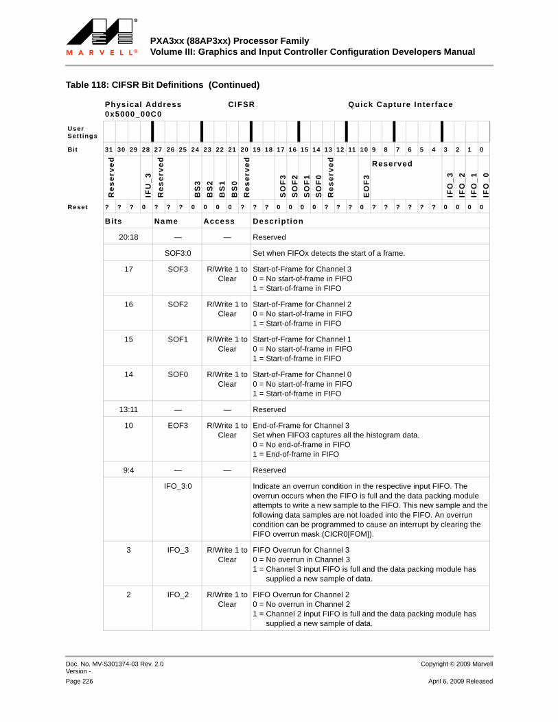
PXA3xx (88AP3xx) Processor FamilyVolume III: Graphics and Input Controller Configuration Developers Manual
Doc. No. MV-S301374-03 Rev. 2.0 Version -
Copyright © 2009 Marvell
Page 226 April 6, 2009 Released
12345678910111213141516171819202122232425262728293031323334353637383940414243444546474849505152535455565758
20:18 — — Reserved
SOF3:0 Set when FIFOx detects the start of a frame.
17 SOF3 R/Write 1 to Clear
Start-of-Frame for Channel 30 = No start-of-frame in FIFO1 = Start-of-frame in FIFO
16 SOF2 R/Write 1 to Clear
Start-of-Frame for Channel 20 = No start-of-frame in FIFO1 = Start-of-frame in FIFO
15 SOF1 R/Write 1 to Clear
Start-of-Frame for Channel 10 = No start-of-frame in FIFO 1 = Start-of-frame in FIFO
14 SOF0 R/Write 1 to Clear
Start-of-Frame for Channel 00 = No start-of-frame in FIFO1 = Start-of-frame in FIFO
13:11 — — Reserved
10 EOF3 R/Write 1 to Clear
End-of-Frame for Channel 3Set when FIFO3 captures all the histogram data.0 = No end-of-frame in FIFO1 = End-of-frame in FIFO
9:4 — — Reserved
IFO_3:0 Indicate an overrun condition in the respective input FIFO. The overrun occurs when the FIFO is full and the data packing module attempts to write a new sample to the FIFO. This new sample and the following data samples are not loaded into the FIFO. An overrun condition can be programmed to cause an interrupt by clearing the FIFO overrun mask (CICR0[FOM]).
3 IFO_3 R/Write 1 to Clear
FIFO Overrun for Channel 30 = No overrun in Channel 31 = Channel 3 input FIFO is full and the data packing module has
supplied a new sample of data.
2 IFO_2 R/Write 1 to Clear
FIFO Overrun for Channel 20 = No overrun in Channel 21 = Channel 2 input FIFO is full and the data packing module has
supplied a new sample of data.
Table 118: CIFSR Bit Definitions (Continued)
Physical Address0x5000_00C0
CIFSR Quick Capture Interface
User Settings
Bit 31 30 29 28 27 26 25 24 23 22 21 20 19 18 17 16 15 14 13 12 11 10 9 8 7 6 5 4 3 2 1 0
Re
se
rve
d
IFU
_3
Re
se
rve
d
BS
3
BS
2
BS
1
BS
0
Re
se
rve
d
SO
F3
SO
F2
SO
F1
SO
F0
Re
se
rve
d
EO
F3
Reserved
IFO
_3
IFO
_2
IFO
_1
IFO
_0
Reset ? ? ? 0 ? ? ? 0 0 0 0 ? ? ? 0 0 0 0 ? ? ? 0 ? ? ? ? ? ? 0 0 0 0
Bits Name Access Description

Quick Capture InterfaceRegister Descriptions
Copyright © 2009 Marvell Doc. No. MV-S301374-03 Rev. 2.0Version -
April 6, 2009 Released Page 227
12345678910111213141516171819202122232425262728293031323334353637383940414243444546474849505152535455565758
3.5.26 Quick Capture Interface FIFO Control Register 0 (CIFR0)CIFR0, shown in Table 119, contain bits that control the behavior of input FIFOs as well as bit fields that indicate the number of bytes in the FIFOs. These are read/write registers. Ignore reads from reserved bits. Write 0b0 to reserved bits.
1 IFO_1 R/Write 1 to Clear
FIFO Overrun for Channel 10 = No overrun in Channel 11 = Channel 1 input FIFO is full and the data packing module has
supplied a new sample of data.
0 IFO_0 R/Write 1 to Clear
FIFO Overrun for Channel 00 = No overrun in Channel 01 = Channel 0 input FIFO is full and the data packing module has
supplied a new sample of data.
Table 118: CIFSR Bit Definitions (Continued)
Physical Address0x5000_00C0
CIFSR Quick Capture Interface
User Settings
Bit 31 30 29 28 27 26 25 24 23 22 21 20 19 18 17 16 15 14 13 12 11 10 9 8 7 6 5 4 3 2 1 0
Re
se
rve
d
IFU
_3
Re
se
rve
d
BS
3
BS
2
BS
1
BS
0
Re
se
rve
d
SO
F3
SO
F2
SO
F1
SO
F0
Re
se
rve
d
EO
F3
Reserved
IFO
_3
IFO
_2
IFO
_1
IFO
_0
Reset ? ? ? 0 ? ? ? 0 0 0 0 ? ? ? 0 0 0 0 ? ? ? 0 ? ? ? ? ? ? 0 0 0 0
Bits Name Access Description
Table 119: CIFR0 Bit Definitions
Physical Address0x5000_00B0
CIFR0 Quick Capture Interface
User Settings
Bit 31 30 29 28 27 26 25 24 23 22 21 20 19 18 17 16 15 14 13 12 11 10 9 8 7 6 5 4 3 2 1 0
Re
se
rve
d FLVL2 FLVL1 FLVL0 Reserved
RE
SE
TF
FE
N2
FE
N1
FE
N0
Reset ? ? 0 0 0 0 0 0 0 0 0 0 0 0 0 0 0 0 0 0 0 0 0 0 ? ? ? ? 0 0 0 0
Bits Name Access Descript ion
31:30 — — Reserved
FLV2:0 Indicate the number of bytes in Channel 0, Channel 1, and Channel 2 FIFOs, respectively. Writes to FLVL fields are ignored. Poll FLVL values to determine the number of bytes remaining to be read in each FIFO.
29:23 FLVL2 R FIFO 2 LevelValue (from 0 to 64) indicates the number of bytes stored in FIFO_2.

PXA3xx (88AP3xx) Processor FamilyVolume III: Graphics and Input Controller Configuration Developers Manual
Doc. No. MV-S301374-03 Rev. 2.0 Version -
Copyright © 2009 Marvell
Page 228 April 6, 2009 Released
12345678910111213141516171819202122232425262728293031323334353637383940414243444546474849505152535455565758
22:16 FLVL1 R FIFO 1 LevelValue (from 0 to 64) indicates the number of bytes stored in FIFO_1.
15:8 FLVL0 R FIFO 0 LevelValue (from 0 to 128) indicates the number of bytes stored in FIFO_0.
7:4 — — Reserved
3 RESETF R/W Reset Input FIFOsResets the FIFO pointers of all four FIFOs. This bit is automatically cleared automatically after the pointers are reset.0 = No effect1 = Resets the input FIFOs.
FEN2:0 FIFO EnableThe enable bits for FIFOs in Channel 0, Channel 1, and Channel 2, respectively. All the FIFOs must be enabled only in planarized YCbCr mode of operation. In this mode, the Channel 0 FIFO holds the Y component, the Channel 1 FIFO holds the Cb component, and the Channel 2 FIFO holds the Cr component. In all other modes, only the Channel 0 FIFO is used to hold the captured data, and Channel 1 and Channel 2 FIFOs are disabled.
2 FEN2 R/W FIFO Enable for Channel 20 = FIFO not enabled for Channel 21 = FIFO enabled for Channel 2
1 FEN1 R/W FIFO Enable for Channel 10 = FIFO not enabled for Channel 1.1 = FIFO enabled for Channel 1.
0 FEN0 R/W FIFO Enable for Channel 00 = FIFO not enabled for Channel 0.1 = FIFO enabled for Channel 0.
Table 119: CIFR0 Bit Definitions (Continued)
Physical Address0x5000_00B0
CIFR0 Quick Capture Interface
User Settings
Bit 31 30 29 28 27 26 25 24 23 22 21 20 19 18 17 16 15 14 13 12 11 10 9 8 7 6 5 4 3 2 1 0
Re
se
rve
d FLVL2 FLVL1 FLVL0 Reserved
RE
SE
TF
FE
N2
FE
N1
FE
N0
Reset ? ? 0 0 0 0 0 0 0 0 0 0 0 0 0 0 0 0 0 0 0 0 0 0 ? ? ? ? 0 0 0 0
Bits Name Access Descript ion

Quick Capture InterfaceRegister Descriptions
Copyright © 2009 Marvell Doc. No. MV-S301374-03 Rev. 2.0Version -
April 6, 2009 Released Page 229
12345678910111213141516171819202122232425262728293031323334353637383940414243444546474849505152535455565758
3.5.27 Quick Capture Interface FIFO Control Register 1 (CIFR1)CIFR1, shown in Table 120, contain bits that control the behavior of input FIFOs as well as bit fields that indicate the number of bytes in the FIFOs. These are read/write registers. Ignore reads from reserved bits. Write 0b0 to reserved bits.
3.5.28 Quick Capture Interface Controller DMA RegistersThe Quick Capture Interface controller has four fully independent DMA channels to transfer data to/from the internal or external memory. DMA channels 0, 1, and 2 are used for the capture data. DMA Channel 3 is used to fetch data from memory for the compander RAM and store data in the histogram unit. All information for the DMA transfers is maintained in registers in the Quick Capture Interface DMA controller. These registers are loaded from frame Descriptors in main memory. Typically, one Descriptor is used for each frame in memory. Multiple Descriptors can be chained together in a list so that the DMA controller can transfer data from a (essentially infinite) number of discontinuous locations.
3.5.28.1 DMA DescriptorsAlthough the CIDADRx registers are loaded by software, the CISADRx, CITADRx, and CICMDx registers can be loaded only indirectly from DMA frame Descriptors. A frame Descriptor is a four-word (32-bit/word) block aligned on a 16-byte boundary in main memory:
Word[0] contains the value for the CIDADRx register.Word[1] contains the value for the CISADRx register.
Word[2] contains the value for the CITADRx register.Word[3] contains the value for the CICMDx register.
Software must write the location of the first Descriptor to the CIDADRx registers before enabling the Quick Capture Interface. When the Quick Capture Interface is enabled, the first Descriptor is read and the DMA controller writes to all four registers. The next frame Descriptor to which the CIDADRx
Table 120: CIFR1 Bit Definitions
Physical Address0x5000_00B4
CIFR1 Quick Capture Interface
User Settings
Bit 31 30 29 28 27 26 25 24 23 22 21 20 19 18 17 16 15 14 13 12 11 10 9 8 7 6 5 4 3 2 1 0
Reserved FLVL3
FE
N3
Reset ? ? ? ? ? ? ? ? ? ? ? ? ? ? ? ? ? ? ? ? ? ? ? 0 ? ? 0 0 0 0 0 0
Bits Name Access Descript ion
31:9 — — Reserved
8:1 FLVL3 R FIFO 3 LevelIndicates the number of bytes in the Channel 3 FIFO. Writes to FLVL fields are ignored. Poll the FLVL3 value to determine the number of bytes remaining to be read in the FIFO.Value (from 0 to 64) indicates number of bytes in FIFO_3
0 FEN3 R/W FIFO Enable for Channel 3The enable bit for the FIFO in Channel 3. The Channel 3 FIFO must be enabled for both metering and companding an image. 0 = FIFO not enabled for Channel 3.1 = FIFO enabled for Channel 3.

PXA3xx (88AP3xx) Processor FamilyVolume III: Graphics and Input Controller Configuration Developers Manual
Doc. No. MV-S301374-03 Rev. 2.0 Version -
Copyright © 2009 Marvell
Page 230 April 6, 2009 Released
12345678910111213141516171819202122232425262728293031323334353637383940414243444546474849505152535455565758
register points is loaded into the registers of the associated DMA channel after all the data for the current Descriptor is transferred. The CIDADRx registers are bypassed only when the branch register (CIFBRx) branch (BRA) bit is set. The branch address is used to fetch the Descriptor for the next frame. Branches can be used to process a regular frame. If only one frame buffer is used in external memory, a Descriptor must be programmed to point back to itself.
3.5.28.2 Quick Capture Interface DMA Descriptor Address Registers (CIDADRx)CIDADRx, shown in Table 121, contain the memory address of the next Descriptor for the channel. The DMA controller fetches the Descriptor at this location after finishing the current Descriptor. The bits in this register are undefined at powerup. The target address needs to be aligned to a 128-bit (16-byte) boundary, so bits 3:0 of the address are reserved. This register should be programmed only when the capture interface is idle. These are read/write registers. Ignore reads from reserved bits. Write 0b0 to reserved bits.
3.5.28.3 Quick Capture Interface DMA Source Address Registers (CISADRx)CISADRx, shown in Table 122, contain the source address of the current Descriptor as defined in the CIDADRx register for the channel. The register should point to the beginning of the frame data in memory. This address is incremented as the DMA controller fetches from memory. See Table 122. These are read-only registers. Ignore reads from reserved bits.
Table 121: CIDADRx Bit Definitions
Physical Address0x5000_02400x5000_02500x5000_02600x5000_0270
CIDADR0CIDADR1CIDADR2CIDADR3
Quick Capture Interface
User Settings
Bit 31 30 29 28 27 26 25 24 23 22 21 20 19 18 17 16 15 14 13 12 11 10 9 8 7 6 5 4 3 2 1 0
Descriptor Address Reserved
Reset 0 0 0 0 0 0 0 0 0 0 0 0 0 0 0 0 0 0 0 0 0 0 0 0 0 0 0 0 ? ? ? ?
Bits Name Access Descript ion
31:4 Descriptor Address
R/W Address of next Descriptor
3:0 — — Reserved

Quick Capture InterfaceRegister Descriptions
Copyright © 2009 Marvell Doc. No. MV-S301374-03 Rev. 2.0Version -
April 6, 2009 Released Page 231
12345678910111213141516171819202122232425262728293031323334353637383940414243444546474849505152535455565758
3.5.28.4 Quick Capture Interface DMA Target Address Registers (CITADRx)CITADRx, shown in Table 123, contain the target address of the current Descriptor for that channel. The address must be aligned on a 128-bit (16-byte) boundary. If this Descriptor is for pixel data, this register should point to the beginning of the frame data in memory. This address is incremented as the DMA controller fetches from memory. See Table 122. These are read-only registers. Ignore reads from reserved bits.
3.5.28.5 Quick Capture Interface DMA Command Registers (CICMDx)CICMDx, shown in Table 124, contain the command and length of the current Descriptor for that channel. See Table 124 and Table 125. These are read-only registers. Ignore reads from reserved bits.
Table 122: CISADRx Bit Definitions
Physical Address0x5000_02440x5000_02540x5000_02640x5000_0274
CISADR0CISADR1CISADR2CISADR3
Quick Capture Interface
User Settings
Bit 31 30 29 28 27 26 25 24 23 22 21 20 19 18 17 16 15 14 13 12 11 10 9 8 7 6 5 4 3 2 1 0
Frame Source Address Reserved
Reset 0 0 0 0 0 0 0 0 0 0 0 0 0 0 0 0 0 0 0 0 0 0 0 0 0 0 0 0 ? ? ? ?
Bits Name Access Description
31:3 Frame Source Address
R Source AddressAddress of the pixel data in memory.
2:0 — — Reserved
Table 123: CITADRx Bit Definitions
Physical Address0x5000_02480x5000_02580x5000_02680x5000_0278
CITADR0CITADR1CITADR2CITADR3
Quick Capture Interface
User Settings
Bit 31 30 29 28 27 26 25 24 23 22 21 20 19 18 17 16 15 14 13 12 11 10 9 8 7 6 5 4 3 2 1 0
Target Address Reserved
Reset 0 0 0 0 0 0 0 0 0 0 0 0 0 0 0 0 0 0 0 0 0 0 0 0 0 0 0 0 ? ? ? ?
Bits Name Access Descript ion
31:3 Target Address
R Target AddressAddress of the data in memory.
2:0 — — Reserved

PXA3xx (88AP3xx) Processor FamilyVolume III: Graphics and Input Controller Configuration Developers Manual
Doc. No. MV-S301374-03 Rev. 2.0 Version -
Copyright © 2009 Marvell
Page 232 April 6, 2009 Released
12345678910111213141516171819202122232425262728293031323334353637383940414243444546474849505152535455565758
Table 124: CICMDx Bit Definitions
Physical Address0x5000_024C0x5000_025C0x5000_026C
CICMD0CICMD1CICMD2
Quick Capture Interface
User Settings
Bit 31 30 29 28 27 26 25 24 23 22 21 20 19 18 17 16 15 14 13 12 11 10 9 8 7 6 5 4 3 2 1 0
Re
se
rve
d
Inc
Trg
Ad
dr
Reserved
SO
FIn
t
Re
se
rve
d Length Reserved
Reset ? 0 ? ? ? ? ? ? ? 0 ? 0 0 0 0 0 0 0 0 0 0 0 0 0 0 0 0 0 0 ? ? ?
Bits Name Access Descript ion
31 — — Reserved
30 IncTrgAddr R Target Address Increment SettingSpecifies whether to increment the target address. For example, if the target address is an internal peripheral FIFO address or external I/O address, the address is not to be incremented on each successive access, and IncTrgAddr must be cleared.0 = Do not increment target address1 = Increment target address
29:23 — — Reserved
22 SOFInt R Start-of-Frame Interrupt MaskWhen set, signals the DMA controller to generate an interrupt when the start-of-frame (SOF) bit in the Quick Capture Interface FIFO Status register is set. The bit is set after a new Descriptor is loaded from memory and before the frame data is fetched.0 = Do not set SOF.1 = Generate an interrupt after the frame Descriptor is loaded.
21 — — Reserved
20:3 Length R Transfer LengthInstructs the DMA controller how many bytes to fetch. LENGTH should be programmed with the size of the 32-bit word data. The value of LENGTH for frame data is a function of the screen size and the pixel size. Setting LENGTH = 0 is invalid. The transfer length must be 8-byte aligned, so the three lowest bits CICMD[2:0] must always be zero for proper alignment. Writes to these three lower bits should be zeros.
2:0 — — Reserved

Quick Capture InterfaceRegister Descriptions
Copyright © 2009 Marvell Doc. No. MV-S301374-03 Rev. 2.0Version -
April 6, 2009 Released Page 233
12345678910111213141516171819202122232425262728293031323334353637383940414243444546474849505152535455565758
3.5.28.6 Quick Capture Interface DMA Branch Registers (CIDBRx)CIFBRx, shown in Table 126, contain the address of the Descriptor to branch to (aligned on a 4-byte boundary). When this register is written and BRA = 1 is set, the Quick Capture Interface Descriptor Address register (CIDADR) is ignored and the next Descriptor is fetched from the address in this register. Setting BINT causes the DMA controller to set the branch-status interrupt bit (BS) in the
Table 125: CICMD3 Bit Definitions
Physical Address0x5000_027C
CICMD3 Quick Capture Interface
User Settings
Bit 31 30 29 28 27 26 25 24 23 22 21 20 19 18 17 16 15 14 13 12 11 10 9 8 7 6 5 4 3 2 1 0
Re
se
rve
d
Inc
Trg
Ad
dr
Reserved
SO
FIn
t
Re
se
rve
d LENGTH
Re
se
rve
d
Reset ? 0 ? ? ? ? ? ? ? 0 ? 0 0 0 0 0 0 0 0 0 0 0 0 0 0 0 0 0 0 ? ? ?
Bits Name Access Descript ion
31 — — Reserved
30 IncTrgAddr R Target Address Increment SettingSpecifies whether to increment the target address. For example, if the target address is an internal peripheral FIFO address or external I/O address, the address is not to be incremented on each successive accesses. In these cases, IncTrgAddr must be cleared.0 = Do not increment target address1 = Increment target address at the end of each internal-bus
transaction initiation by the size of the transfer
29:23 — Reserved
22 SOFInt R Start-of-Frame Interrupt MaskWhen set, signals the DMA controller to generate an interrupt when the start-of-frame (SOF) bit in the Quick Capture Interface FIFO Status register is set. The bit is set after a new Descriptor is loaded from memory and before the frame data is fetched.0 = Generate an interrupt after the frame Descriptor is loaded.1 = Do not set SOF.
21 — — Reserved
20:3 LENGTH R Transfer LengthInstructs the DMA controller how many bytes to fetch. LENGTH should be programmed with the size of the 32-bit word data. Programming for HST writes to memory, the LENGTH value must be either 512 or 1024 depending on CIHST[SCALE]. The value of LENGTH for CGC LUT loading should be 64 bytes for each LUT address space (red, blue, green). Clearing LENGTH is not valid. The transfer length must be 8-byte aligned, so the three lowest bits CICMD[2:0] must always be zero for proper alignment. Writes to these three lower bits should be zeroes.
2:0 — — Reserved

PXA3xx (88AP3xx) Processor FamilyVolume III: Graphics and Input Controller Configuration Developers Manual
Doc. No. MV-S301374-03 Rev. 2.0 Version -
Copyright © 2009 Marvell
Page 234 April 6, 2009 Released
12345678910111213141516171819202122232425262728293031323334353637383940414243444546474849505152535455565758
Quick Capture Interface Status register after fetching the branched-to Descriptor. Hardware automatically clears the BRA bit when the branch is taken. These are read/write registers. Ignore reads from reserved bits. Write 0b0 to reserved bits.
3.5.28.7 DMA Channel Control/Status Register (CIDCSRx)CIDCSRx, shown in Table 127, contains the control and status bit for the channel. These are read/write registers. Ignore reads from reserved bits. Write 0b0 to reserved bits.
Table 126: CIFBRx Bit Definitions
Physical Addresses0x5000_0220 0x5000_02240x5000_02280x5000_022C
CIFBR0CIFBR1CIFBR2CIFBR3
Quick Capture Interface
User Settings
Bit 31 30 29 28 27 26 25 24 23 22 21 20 19 18 17 16 15 14 13 12 11 10 9 8 7 6 5 4 3 2 1 0
SrcAddr
Re
se
rve
d
BIN
T
BR
A
Reset 0 0 0 0 0 0 0 0 0 0 0 0 0 0 0 0 0 0 0 0 0 0 0 0 0 0 0 0 ? ? 0 0
Bits Name Access Descript ion
31:4 SrcAddr R/W Branch AddressAddress of the Descriptor for the branched-to frame.
3:2 — — Reserved
1 BINT R/W Branch Status InterruptSpecifies whether to set the branch status (BS) bit in the Quick Capture Interface FIFO Status register (CIFSR) after the branched-to Descriptor is loaded.0 = Do not set the BS bit.1 = Set branch status (BS) interrupt bit.
0 BRA R/W 0 = Do not branch.1 = Branch after finishing the current frame. The next Descriptor is
fetched from the Branch Address. This bit is automatically cleared after the new Descriptor is loaded.

Quick Capture InterfaceRegister Descriptions
Copyright © 2009 Marvell Doc. No. MV-S301374-03 Rev. 2.0Version -
April 6, 2009 Released Page 235
12345678910111213141516171819202122232425262728293031323334353637383940414243444546474849505152535455565758
Table 127: CIDCSRx Bit Definitions
Physical Address0x5000_02000x5000_02040x5000_02080x5000_020C
CIDCSR0CIDCSR1CIDCSR2CIDCSR3
Quick Capture Inter face
User Settings
Bit 31 30 29 28 27 26 25 24 23 22 21 20 19 18 17 16 15 14 13 12 11 10 9 8 7 6 5 4 3 2 1 0
Re
se
rve
d
Sto
pIr
qE
n Reserved
Re
qP
en
d Reserved
Sto
pIn
tr
Re
se
rve
d
Bu
sE
rrIn
tr
Reset ? ? 0 ? ? ? ? ? ? ? ? ? ? ? ? ? ? ? ? ? ? ? ? 0 ? ? ? ? 0 0 0 0
Bits Name Access Descript ion
31:30 — — Reserved
29 StopIrqEn R/W Stop Channel Interrupt MaskEnables the interrupt when StopIntr is set. If StopIrqEn is cleared, no interrupt is generated after the channel stops. Setting this bit enables the interrupt. StopIntr is set after a system reset deassertion, so if software sets this bit before the channel is started, an interrupt is generated.0 = No interrupt if the channel is in uninitialized or stopped state.1 = Enable the interrupt if the channel is in uninitialized or stopped
state.
28:9 — — Reserved
8 ReqPend R Internal Request PendingIndicates that the DMA channel has a pending request. The bit associated with a channel is 0b1 if that channel has a pending request, and 0b0 if that channel has no pending request or the request has just been issued to the memory interface. 0 = No pending request1 = The channel has a pending request.
7:4 — — Reserved
3 StopIntr R Stop Interrupt Channel 0Reflects whether the channel is in initialized or stopped state. This bit is set after reset deassertion. If the channel is in uninitialized or stopped state, StopIntr is set. If StopIrqEn is set, the DMA controller generates an interrupt. The channels must be configured prior to data transfer as described in Section 3.4.5.2. If the Descriptor address is not set up before threshold levels are reached, StopIntr is set. The channel 3. Clear StopIrqEn to reset the interrupt. 0 = Channel is running1 = Channel is in uninitialized or stopped state.
2:1 — — Reserved
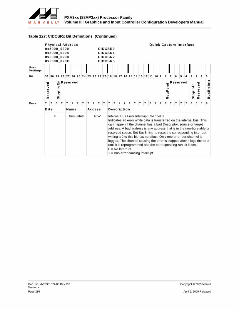
PXA3xx (88AP3xx) Processor FamilyVolume III: Graphics and Input Controller Configuration Developers Manual
Doc. No. MV-S301374-03 Rev. 2.0 Version -
Copyright © 2009 Marvell
Page 236 April 6, 2009 Released
12345678910111213141516171819202122232425262728293031323334353637383940414243444546474849505152535455565758
0 BusErrIntr R/W Internal Bus Error Interrupt Channel 0Indicates an error while data is transferred on the internal bus. This can happen if the channel has a bad Descriptor, source or target address. A bad address is any address that is in the non-burstable or reserved space. Set BusErrIntr to reset the corresponding interrupt; writing a 0 to this bit has no effect. Only one error per channel is logged. The channel causing the error is stopped after it logs the error until it is reprogrammed and the corresponding run bit is set.0 = No interrupt1 = Bus error causing interrupt
Table 127: CIDCSRx Bit Definitions (Continued)
Physical Address0x5000_02000x5000_02040x5000_02080x5000_020C
CIDCSR0CIDCSR1CIDCSR2CIDCSR3
Quick Capture Inter face
User Settings
Bit 31 30 29 28 27 26 25 24 23 22 21 20 19 18 17 16 15 14 13 12 11 10 9 8 7 6 5 4 3 2 1 0
Re
se
rve
d
Sto
pIr
qE
n Reserved
Re
qP
en
d Reserved
Sto
pIn
tr
Re
se
rve
d
Bu
sE
rrIn
tr
Reset ? ? 0 ? ? ? ? ? ? ? ? ? ? ? ? ? ? ? ? ? ? ? ? 0 ? ? ? ? 0 0 0 0
Bits Name Access Descript ion

Graphics ControllerFeatures
Copyright © 2009 Marvell Doc. No. MV-S301374-03 Rev. 2.0Version -
April 6, 2009 Released Page 237
12345678910111213141516171819202122232425262728293031323334353637383940414243444546474849505152535455565758
4 Graphics ControllerThis chapter presents requirements, functions, and architecture of the graphics controller, which performs basic 2-D graphics instructions on two possible source data buffers and three possible destination data buffers.
4.1 FeaturesThe graphics controller features include:
Graphics instruction list parserTwo source buffersThree destination buffers (including internal and external display buffers (front/back buffers))
Support for multiple pixel formats8-bit to 64-bit color1-bit transparency or 16-bit alpha
2-D graphics accelerationAlpha blend BLT (BLock Transfer)Scale BLT
Bias BLTChroma key BLTStretch BLT
Decimate BLTLine drawAnti-aliased line draw
Rotate BLTRaster OP BLT (serves as source copy BLT)Pattern copy BLT
Color fillLocal buffer to reduce bus bandwidth for 2-D operationsPixel ALU
Eight 64-bit storage registersThree 16-bit channels for pixel data operationsPixel format conversion support
Pixel multiplier/accumulator processing architectureSupport for alpha and transparency operationsFull raster operation support
4.2 I/O SignalsNo external I/O signals are associated with the graphics controller.
4.3 System OverviewThe graphics controller interfaces with memory and with the core through internal System Bus 2 and the switch structure block (see Figure 55).

PXA3xx (88AP3xx) Processor FamilyVolume III: Graphics and Input Controller Configuration Developers Manual
Doc. No. MV-S301374-03 Rev. 2.0 Version -
Copyright © 2009 Marvell
Page 238 April 6, 2009 Released
12345678910111213141516171819202122232425262728293031323334353637383940414243444546474849505152535455565758
Figure 55: Basic Processor Architecture
4.4 Buffer Operation OverviewFigure 56 shows the graphics controller and the buffers with which it operates. An operation generally consists of performing 2-D graphics instructions on data from two source buffers and one of three bidirectional destination buffers. The result is stored in the same destination buffer. Two of the three destination buffers should be used as the Display Front buffer and Display Back buffer. The third destination buffer can be anywhere in memory. Similarly, there are no constraints on the two source buffers. They can be located anywhere in memory.
There are two types of buffers for holding graphics instructions, ring buffer and batch buffer. The ring buffer stores a circular list of instructions and is always used. The instructions can point to external batch buffers, which are separate buffers to hold specialized groups of instructions and are analogous to software subroutines. After the graphics controller is configured and enabled, the graphics controller hardware automatically reads from the ring and (optionally) the batch buffers.
Software must specify the locations of the source and destination buffers, including which is the current destination buffer, by programming the Graphics Controller Configuration Register (GCCR), which is described in Section 4.7.1, Graphics Controller Configuration Register (GCCR), on page 348. The locations of the source and destination buffers and the current destination buffer can also be specified by the graphics controller Buffer Info instruction (see Section 4.6.1.3) and Buffer Flip instruction (see Section 4.6.1.6).
Core
Memory
System BusModule 1
System BusModule 2
LCD
Quick
GraphicsController
Unit
System Bus 1
System Bus 2
InternalSRAM
ExternalMemory
ScratchPad
SRAM
PR
OC
ES
SO
R B
OU
ND
AR
Y
CH
IP B
OU
ND
AR
Y
Switch
InterfaceCapture

Graphics ControllerBuffer Operation Overview
Copyright © 2009 Marvell Doc. No. MV-S301374-03 Rev. 2.0Version -
April 6, 2009 Released Page 239
12345678910111213141516171819202122232425262728293031323334353637383940414243444546474849505152535455565758
Figure 56: General Graphics Controller Buffer Configuration
4.4.1 Programming the Source Buffer RegistersThe source buffer 0 and source buffer 1 registers are programmed the same way. Both sets of registers are programmed with the base address, step size, stride size and pixel format. The source buffer 0 registers are as follows:
Graphics Controller Source 0 Base Address Register (GCS0BR), Section 4.7.27.Graphics Controller Source 0 Step Size Register (GCS0STP), Section 4.7.28.
Graphics Controller Source 0 Stride Size Register (GCS0STR), Section 4.7.29.Graphics Controller Source 0 Pixel Format Register (GCS0PF), Section 4.7.30.
These registers have source 1 counterparts, GCS1BR, GCS1STP, GCS1STR, and GCS1PF. There are two ways to program all of these registers (see Figure 57):
Write the configuration values directly to the graphics controller. Use the GC_BUFFI graphics instruction to send the configuration values to the source buffer 0 registers (and to the source buffer 1 registers at the same time, if needed).
Boerne
Graphics Controller
Source 0 Buffer
Source 1 Buffer
Destination 0 Buffer(Display Buffer 0)
Destination 1 Buffer(Display Buffer 1)
Destination 2 BufferGraphicsController
2-D Instruction
DestinationBuffer
Current
Ring Buffer
Batch Buffer 0
Batch Buffer n
BoerneGraphicsController
Instruction Decode
BoerneGraphicsController
Scratchpad SRAM
Engine
3 × 128 × 64 bits1 × 128 × 72 bits

PXA3xx (88AP3xx) Processor FamilyVolume III: Graphics and Input Controller Configuration Developers Manual
Doc. No. MV-S301374-03 Rev. 2.0 Version -
Copyright © 2009 Marvell
Page 240 April 6, 2009 Released
12345678910111213141516171819202122232425262728293031323334353637383940414243444546474849505152535455565758
Figure 57: Programming Flow for Source Buffers Registers
4.4.2 Programming the Destination Buffer RegistersDestination buffer 0, Destination Buffer 1, and Destination Buffer 2 registers are programmed the same way even though buffers 0 and 1 are associated and buffer 2 is separate. If a single-buffered scheme is used for the display buffers, the information programmed into the Destination Buffer 0 and Destination Buffer 1 registers is identical. The pertinent pre-programmed information for each of the three destination buffers is base address, step size, stride size, and pixel format. There are two ways to program all the destination buffers (see Figure 58):
Write the configuration values directly to the GCDxBR, GCDxSTP, GCDxSTR, and GCDxPF registers, respectively, where x = 0, and possibly 1, 2. Use the GC_BUFFI graphics instruction to send the configuration values to the Destination Buffer 0, Destination Buffer 1, and/or Destination Buffer 2 registers. Any information received in the instruction is written to the GCDxBR, GCDxSTP, GCDxSTR, and GCDxPF registers, respectively, where x = 0, and possibly 1 and 2.
GCS0BR
GCS0STP
GCS0STR
GCS1BR
GCS1STP
GCS1STR
Graphics Controller Source Configuration Registers
Graphics Controller Instruction Stream
Internal Bus/Core
InstructionDecoder
GC_BUFFIGCS0PF
GCS1PF

Graphics ControllerFunctional Description
Copyright © 2009 Marvell Doc. No. MV-S301374-03 Rev. 2.0Version -
April 6, 2009 Released Page 241
12345678910111213141516171819202122232425262728293031323334353637383940414243444546474849505152535455565758
Figure 58: Programming Flow for Destination Buffers Registers
When the destination buffer registers are programmed, the current destination buffer method and the current destination buffer must both be selected by programming GCCR[DEST] and GCCR[CURR_DEST], respectively. These bits can be configured in one of two ways:
Software writes to the GCCR.Execution of the GC_DBFLIP destination buffer flip graphics instruction.
See Section 4.6.1.6. If the Destination (display) Buffer Swapping mode is chosen through GCCR[DEST], then configure GCCR[CURR_DEST] to either destination buffer 0 or destination buffer 1, whichever is the display back buffer. See Section 4.5.5.4. Do not change the source or destination buffers after they are configured except through the use of the GC_DBFLIP graphics instruction.
4.5 Functional DescriptionThe graphics controller functional description addresses the following:
Control functionsProgramming environment
GCD0BR
GCD0STP
GCD0STR
Graphics Controller Destination Configuration Registers
Graphics Controller Instruction Stream
Internal Bus / Core
InstructionDecoder
GC_BUFFI
GCD0PF
GCD1BR
GCD1STP
GCD1STR
GCD1PF
GCD2BR
GCD2STP
GCD2STR
GCD2PF
GCCRGC_DBFLIP

PXA3xx (88AP3xx) Processor FamilyVolume III: Graphics and Input Controller Configuration Developers Manual
Doc. No. MV-S301374-03 Rev. 2.0 Version -
Copyright © 2009 Marvell
Page 242 April 6, 2009 Released
12345678910111213141516171819202122232425262728293031323334353637383940414243444546474849505152535455565758
4.5.1 Control FunctionsThe graphics controller can access three different memory spaces (see Figure 55).
External memory. This addressable memory (stacked or non-stacked) is external to the processor.Internal memory. This addressable SRAM memory is located inside the processor but outside the graphics controller. In general, higher performance is achieved using this internal SRAM memory.Local scratchpad SRAM. This memory is located inside the graphics controller. It is not writable or readable outside the graphics controller.
Buffer synchronization must be maintained among the following:
Core
LCD controller Quick Capture Interface controller
Graphics controller
This graphics controller synchronization is achieved by the following:
Internal signals from the LCD controllerInternal signals from the Marvell Quick Capture Interface (QCI) controller
Use of the following graphics controller instructions:
• Destination Buffer Flip (see Section 4.6.1.6)
• Wait for Event (see Section 4.6.1.9)
• Load Register (see Section 4.6.1.4)
• Store Register (see Section 4.6.1.7)
Synchronization signals from the LCD controller and QCI controller are latched in when set by the graphics controller and held asserted until they are used. Then they are automatically reset. Also, software can reset them either by setting the GCCR[SYNC_CLR] bit or by executing the Wait-for-Event graphics instruction. See Section 4.6.1.9 and Section 4.7.1 for more information on clearing the latched signals.
A sample is described below. In the following example instruction stream for synchronization, the graphics controller prepares a value to write to the QCI, waits for the camera to finish capturing a frame, writes the value to the camera, and then changes the graphics buffer to the one just completed by the camera. Use whatever instructions are required to obtain the preferred synchronization results:
1. Load register. Pixel Format = RGBA 8:8:8:8 - Load a specific pixel value into a Pixel ALU Scratchpad register. This value eventually is written to an appropriate Configuration Register in the QCI controller.
2. Wait for event. Wait for a frame-complete status indication from the QCI controller.3. Store register. Pixel Format - RGBA 8:8:8:8 - Store the Pixel ALU Scratchpad Register that was
loaded above to an appropriate Configuration Register in the QCI controller that switches its render Ring buffer for the camera interface.When it receives a Wait-for-Event instruction, the graphics controller stops processing instructions until the defined event occurs.
4. Destination buffer flip. Flip the graphics controller current render ring buffer.
When it receives a Destination Buffer Flip instruction, the graphics controller immediately swaps destination buffers.
For more information on synchronization between the core, LCD controller, QCI controller, and the graphics controller, refer to the individual chapters for the LCD controller and QCI controller.

Graphics ControllerFunctional Description
Copyright © 2009 Marvell Doc. No. MV-S301374-03 Rev. 2.0Version -
April 6, 2009 Released Page 243
12345678910111213141516171819202122232425262728293031323334353637383940414243444546474849505152535455565758
4.5.2 Programming EnvironmentThe processor supports real-time interaction with memory-mapped control and status registers. Graphics instruction-list execution occurs without intervention from the core. The graphics engine uses a single-thread execution model that is monitored and controlled by register Read and Write operations and optionally by interrupts.
4.5.2.1 InterruptsThe graphics controller has eight interrupt-request sources, but only one interrupt request output signal is sent from the graphics controller to the interrupt controller. This interrupt signal can optionally be masked. Each interrupt request has an enable bit and an associated status bit. When an interrupt request condition occurs, the interrupt request status bit (GCISCR[xx_INTST]) is set in the Graphics Controller Interrupt Status Control Register (see Section 4.7.2). The interrupt request output signal from the graphics controller to the interrupt controller (gcu_intr_r) is asserted only if the corresponding interrupt request enable bit (GCIECR[xx_INTEN]) is set in the Graphics Controller Interrupt Enable Control Register (see Section 4.7.3).
The condition causing the interrupt request must be cleared before the interrupt request status bit is cleared; otherwise, the interrupt immediately occurs again. For example, if the ring buffer head reaches the ring buffer tail pointer, the ring buffer tail pointer must be changed before the End of buffer interrupt request is cleared. Otherwise, the End of Buffer condition is still true and the interrupt request is generated again.
The possible graphics interrupt requests are as follows:
End of Buffer. The end of the ring buffer is read from memory—that is, the ring buffer head pointer reaches the ring buffer tail pointer. For information on the operation of the ring buffer, see Section 4.5.5.2. Change the ring buffer tail value before clearing this interrupt request.Execution End of Buffer. The end of the ring buffer is executed—that is, the ring buffer execution head pointer reaches the ring buffer tail pointer. If the last instruction in the ring buffer is a batch buffer start, execution within the batch buffer may still be occurring. Change the ring buffer tail value before clearing this interrupt request.Instruction. A graphics controller interrupt instruction is received in the current execution buffer (either the ring or batch buffer). See Section 4.6.1.8 for details.Destination Buffer Flip. A flip occurs as a result of an event specified in the Destination Buffer Flip instruction (see Section 4.6.1.6).Illegal Graphics Controller Instruction Type. An illegal graphics controller instruction type is received in the current execution buffer. This condition occurs when the GCI Type field of the first word of an instruction does not match that of a defined Control/Memory instruction or a 2-D graphics instruction. See Section 4.6.
Illegal Graphics Controller Instruction Operation. An illegal instruction is received in the current execution buffer because the Opcode field of the first word of an instruction does not match that of a defined Control/Memory instruction or a 2-D graphics instruction. See Section 4.6.Illegal Pixel Format/Step Size. This interrupt request occurs when:
• An illegal pixel format is programmed into a control register or in an instruction in the graphics instruction stream.
• An illegal step size is programmed into a control register.
• The pixel format and step size programmed for a specific source or destination buffer are not consistent with each other.
See Section 4.5.7 for more information on legal and compatible pixel formats and step sizes.
Graphics Controller GCCR[STOP] Response Interrupt. If the graphics controller is programmed to stop all activity after GCCR[STOP] is set, it finishes the instruction being processed and then signals that it has stopped. GCCR[STOP] must be cleared before this interrupt request is cleared.

PXA3xx (88AP3xx) Processor FamilyVolume III: Graphics and Input Controller Configuration Developers Manual
Doc. No. MV-S301374-03 Rev. 2.0 Version -
Copyright © 2009 Marvell
Page 244 April 6, 2009 Released
12345678910111213141516171819202122232425262728293031323334353637383940414243444546474849505152535455565758
4.5.3 Error Conditions: Crash Stops, Breakpoints, and AbortsThe graphics controller handles various types of error conditions, as detailed in this section. Much of the information about which error condition has occurred is contained in the GCU_NOP_ID Register. See Section 4.7.4 and Section 4.6.1.5 for information on this register.
4.5.3.1 Crash StopSoftware can select the graphics controller to perform a crash stop to the debug unit (MDU) by inserting a NOP instruction with the NOP_ID containing the value 0xFFFFF into the graphics execution instruction stream (in a ring or batch buffer). When this NOP instruction executes, it causes the NOP_ID register to be written with the value 0xFFFFF and the graphics controller stops processing instructions. When the crash stop condition is asserted, the only way to clear the condition is to reset the graphics controller. After execution of the crash stop NOP instruction, the graphics controller continues to execute instructions from its buffers as long as the MDU does not stop its execution.
4.5.3.2 Breakpoint OutSoftware can select the graphics controller to assert a breakpoint out to the MDU by inserting a NOP instruction with the NOP_ID containing the value 0xFFFFE into the graphics execution instruction stream (in a ring or batch buffer). When this NOP instruction executes, the NOP_ID register is written with the value 0xFFFFE. When the graphics controller asserts the breakpoint out condition, it can be cleared by setting GCCR[BP_RST]. If a subsequent breakpoint out NOP instruction is received, the NOP_ID register is still written with the value 0xFFFFE. After the breakpoint out NOP instruction executes, the graphics controller continues to execute instructions from its buffers as long as the MDU does not stop its execution.
4.5.3.3 Breakpoint InThe MDU can cause a breakpoint within the graphics controller. The graphics controller finishes the current instruction and then stops all operation. This action is similar to setting GCCR[STOP] or causing the PMU to enter S0/D1/C2 or S0/D2/C2 (see Section 4.5.4).
4.5.3.4 Target AbortsIf the graphics controller is requesting a read or write access over System Bus 2 and the target aborts the operation, the following action occurs:
1. The NOP_ID register is written with the target abort NOP ID value 0xFFFFD.2. The GCTABADDR register is written with the address that the graphics controller was providing
to System Bus 2 when the target abort occurred.3. A target abort is internally signalled:
• If the abort occurs while the graphics controller is fetching ring buffer data, the Ring Buffer Length Register is cleared and all execution within the graphics controller stops.
• If the abort occurs while the graphics controller is fetching batch buffer data, execution jumps back to the ring buffer.
• If the abort occurs while the graphics controller is fetching data for an instruction or storing destination data for an instruction, the execution of that instruction stops and execution jumps to the next instruction in the buffer.
• If the abort occurs while the graphics controller is fetching data for a Load Register from Memory Instruction, the scratch register is not loaded and execution jumps to the next instruction.
• If the abort occurs while the graphics controller is fetching anti-aliasing coefficients for an AALINE instruction, the AALINE instruction is skipped and execution jumps to the next instruction.

Graphics ControllerFunctional Description
Copyright © 2009 Marvell Doc. No. MV-S301374-03 Rev. 2.0Version -
April 6, 2009 Released Page 245
12345678910111213141516171819202122232425262728293031323334353637383940414243444546474849505152535455565758
4.5.3.5 Master AbortsIf the graphics controller is requesting a read or write access over System Bus 2 and no response is received, the graphics controller performs a master abort. The behavior is similar to a target abort, with the following differences:
The NOP_ID register is written with the master abort NOP ID value 0xFFFFC.GCMABADDR is written with the address that the graphics controller was providing to System Bus 2 when the master abort occurred.A master abort is signalled internally.
4.5.3.6 Internal Operation ErrorsThe main cause of unrecoverable errors inside the graphics controller is bad programming—for example, when software tries to execute a Stretch BLT graphics instruction and the programmed width/height do not match the programmed X_str and Y_str values. The data requesting unit finishes requesting source data, but the Pixel ALU is expecting more data. A 16-bit up-counter can be used to detect this type of unrecoverable error. The up-counter begins to count (at the System Bus 2 frequency of either 104 or 208 MHz) when the graphics controller 2-D Address Generator is in an IDLE state. An unrecoverable error occurs when the counter reaches its maximum value of 0xFFFF.
The following actions occur if the GCCR[INT_ERR_EN] bit is set:
The NOP_ID register is written with the Internal Error Enabled NOP ID value 0xFFFFB.Execution jumps to the next instruction in the graphics execution buffer.
The following actions occur if the INT_ERR_EN is cleared:
The NOP_ID register is written with the Internal Error Disabled NOP ID value 0xFFFFA.If software polls the NOP_ID register and gets the NOP ID value 0xFFFFA, software can enable the internal error (set INT_ERR_EN). The graphics controller then performs the error enabled operations when the counter again reaches its maximum value of 0xFFFF value (the counter rolls over upon reaching 0xFFFF and keeps counting). This method takes twice as long for graphics execution to jump to the next instruction.
4.5.3.7 Stop ExecutionSoftware can set GCCR[STOP] to stop operation inside the graphics controller. The graphics controller finishes the current instruction and then halts all instruction execution until software clears GCCR[STOP]. When operation stops, GCISCR[STOP_INTST] is set (if GCIECR[STOP_INTEN] is set) to alert software that the current instruction has finished executing. The ring buffer control register is maintained. Ring buffer fetches can still occur when STOP is set, but the instructions are not executed. Graphics control register Reads and Writes are still accepted when STOP is set.
Software can disable the clock by clearing the graphics controller clock enable bit in the appropriate Clock Control Unit register. Software must use GCCR[STOP] to halt the graphics controller before disabling the clock. When the CPU disables the clock to the graphics controller, it must first set STOP. Next, the graphics controller sets GCISCR[STOP_INTST] and generates an interrupt request if the interrupt is enabled. When the interrupt is set, the core can disable the graphics controller clock. To re-enable the clock, set the clock enable bit in the Clock Control Unit and clear GCCR[STOP]. Graphics control register Reads and Writes are still accepted when the graphics controller clock is disabled.
4.5.3.8 Abort ExecutionSoftware sets GCCR[ABORT] to abort operation. The graphics controller stops the current instruction and halts execution of all further instructions. If a System Bus 2 transaction is in progress, it completes. The ring buffer control registers are cleared. Execution inside the graphics controller does not resume until ABORT is cleared and the ring buffer control registers are reprogrammed.

PXA3xx (88AP3xx) Processor FamilyVolume III: Graphics and Input Controller Configuration Developers Manual
Doc. No. MV-S301374-03 Rev. 2.0 Version -
Copyright © 2009 Marvell
Page 246 April 6, 2009 Released
12345678910111213141516171819202122232425262728293031323334353637383940414243444546474849505152535455565758
These registers cannot be programmed while ABORT is set. Control register Reads and Writes are still accepted when ABORT is set.
4.5.4 Low Power (S0/D1/C2 and S0/D2/C2) If the system enters S0/D1/C2 or S0/D2/C2 mode, the graphics controller finishes the current instruction and halts all instruction operation. All configuration and scratch registers in the graphics controller maintain their values during this time. Ring buffer fetches and configuration register Reads and Writes can still occur while the graphics controller enters the low-power mode. This works much like setting GCCR[STOP].
4.5.5 2-D Graphics Instruction BuffersGraphics instructions are not sent directly to the graphics controller. Rather, software stores them in memory-based ring or batch buffers so that the graphics controller instruction parser can read them later. These buffers can exist in any addressable memory block, but they cannot span different blocks.
There are two basic types of instruction buffers. The ring buffer (see Section 4.5.5.2) is the primary buffer. It passes the bulk of the 2-D graphics instruction stream to the graphics controller. The graphics instructions in the batch buffer (see Section 4.5.5.3) can be fetched only after a Batch Buffer Start instruction (see Section 4.6.1.1) in the ring buffer or another batch buffer executes.
4.5.5.1 Basic Queue Structure OperationThe graphics controller operates the ring and batch buffers as basic queue structures; that is, as FIFO storage structures that circle back on themselves. The head pointer points to the location of the next instruction to read into the internal instruction queue. The tail pointer points to the memory location to which to write the next new instruction. The execution pointer points to the location of the graphics instruction executing in the graphics controller.
Before the graphics controller begins operation, the head, tail and execution pointers all point to the same location. Instructions are written to the location specified by the tail pointer, which increments as the Writes occur. As the graphics controller loads the instructions into the internal instruction queue, the head pointer moves towards the tail pointer. As the instructions in the internal instruction queue execute, the execution head pointer moves, indicating which instruction is executing.
The example queue in this section stores a single byte. Figure 60 shows the beginning (head pointer) and end (tail pointer) for six instruction bytes in a queue that is 8 bytes long. Information is written into and read out of the queue structure. A Write to a queue structure occurs at the location to which the tail pointer is pointing. At the end of the Write operation, the tail pointer increments by 1. If this pointer is currently at the end of the queue, incrementing it causes it to circle back and point to the beginning of the queue, see Figure 63).
A Read from a queue structure (see Figure 62) occurs at the location to which the head pointer is pointing. At the end of the Read operation, the head pointer then increments by 1. If the head pointer is currently at the end of the queue, incrementing it causes it to circle back and point to the beginning of the queue.
A Read cannot occur if the head pointer and the tail pointer have the same value, which signifies an empty queue (see Figure 59). Similarly, a Write cannot occur if the value of the tail pointer is one less than the value of the head pointer, which signifies a full queue (see Figure 61). Because no full or empty bits are associated with a specific location in the ring buffer, the ring buffer can never be completely full. For example, in Figure 61, the length of the queue structure is 8, and no more than 7 instructions can be stored.
In general, the following formulas apply for the graphics controller queue-styled ring and batch buffers:
Empty Queue → HEAD = TAIL

Graphics ControllerFunctional Description
Copyright © 2009 Marvell Doc. No. MV-S301374-03 Rev. 2.0Version -
April 6, 2009 Released Page 247
12345678910111213141516171819202122232425262728293031323334353637383940414243444546474849505152535455565758
Full Queue →
• If TAIL = (LENGTH – 1), then Full Queue when TAIL+1 – LENGTH = HEAD
• Else, Full Queue when TAIL + 1 = HEAD
Write to Queue →• If TAIL = (LENGTH – 1), then TAIL = BASE (0 in example)
• Else, TAIL = TAIL + 1
Read from Queue →• If HEAD = (LENGTH – 1), then HEAD = BASE (0 in example)
• Else, HEAD = HEAD + 1
Figure 59: Empty Queue (Head = Tail)
Figure 60: Queue of Length 8 Containing 6 Instructions (Tail – Head = 6)
Figure 61: Basic Write to Queue (Tail = Tail + 1); Full Queue (Tail + 1 – Length =
Head)
Head = 0
Tail = 0
FF FF FF FF FF FF FF FF
0 1 2 3 4 5 6 7
Head = 0Tail = 6
01 23 45 67 89 AB FF FF
0 1 2 3 4 5 6 7
Head = 0Tail = 7
01 23 45 67 89 AB CD FF
0 1 2 3 4 5 6 7

PXA3xx (88AP3xx) Processor FamilyVolume III: Graphics and Input Controller Configuration Developers Manual
Doc. No. MV-S301374-03 Rev. 2.0 Version -
Copyright © 2009 Marvell
Page 248 April 6, 2009 Released
12345678910111213141516171819202122232425262728293031323334353637383940414243444546474849505152535455565758
Figure 62: Basic Read from Queue (Head = Head + 1)
Figure 63: Wrap-around Write to Queue (new Tail = 0); Full Queue (Tail + 1 = Head)
4.5.5.2 Ring BufferThe graphics controller operates the ring buffer as a basic queue structure (see Section 4.5.5.1). The ring buffer parameters are communicated to the graphics controller by a set of registers (and the actual memory region containing the instructions). Software or graphics instructions write to the graphics controllers ring buffer control registers to specify the buffer base address, instruction byte length, and tail pointer. Software must monitor the Head Pointer register and the Execution HEAD Pointer register for the ring buffer. Writing directly to the HEAD Pointer and Execution Head Pointer registers is not allowed. Instead, these registers are automatically initialized to the ring buffer base address when software writes it to the Ring Buffer Base register. The general flow for setting up the ring buffer is as follows:
1. Program the ring buffer length to 0.2. Program the Ring Buffer Base register to the beginning of the ring buffer location in memory.
This automatically programs the Ring Buffer Head and Ring Buffer Execution Head registers to the same memory location.
3. Program the Ring Buffer Tail register to 1-byte location past the last real byte in the ring buffer.
For example, if the buffer instruction bytes go through address 0x0000002C, the Ring Buffer Tail register is programmed to 0x00000030.
4. Program the Ring Buffer Length register with the location of the ring buffer tail in memory if all instructions are written to the buffer. If more instructions are to be written (increasing the length of the buffer), program the Ring Buffer Length register with a larger value than that of the tail pointer.
The head pointer and tail pointer registers are automatically loaded with the value in the base register, and an End of Buffer Interrupt request is generated under the following conditions:
The buffer tail value is equal to the buffer base value plus the buffer length value minus 4 bytes.The head pointer value reaches the tail pointer value, indicating that all instruction bytes are read.
Head = 1Tail = 7
01 23 45 67 89 AB CD FF
0 1 2 3 4 5 6 7
Head = 1Tail = 0
01 23 45 67 89 AB CD EF
0 1 2 3 4 5 6 7

Graphics ControllerFunctional Description
Copyright © 2009 Marvell Doc. No. MV-S301374-03 Rev. 2.0Version -
April 6, 2009 Released Page 249
12345678910111213141516171819202122232425262728293031323334353637383940414243444546474849505152535455565758
Except for a GCCR[ABORT] (see Section 4.5.3.8) condition, this is the only time the graphics controller changes the value in the Ring Buffer Tail register.
Monitor the End of Buffer and Execution End of Buffer interrupt requests and change the tail, base, and length registers accordingly. If software uses the End of Buffer (Head = Tail) interrupt request as the indication to change the value of the Tail Pointer register, and if doing so causes the ring buffer to wrap around, care must be taken to assure that the new value for the Tail Pointer register does not point beyond the value in the Execution HEAD register (see Figure 64). Otherwise, a false Execution End of Buffer interrupt request is generated.
Figure 64: Programming New Tail in Wrap-Around Mode
Note
Note When switching the base register, as in a double buffered ring buffer implementation, the switch must not take place until the value of the Execution Head Pointer reaches the value of the tail pointer, as indicated by generation of an Execution End of Buffer interrupt request. Otherwise, behavior is indeterminate.
Graphics Controller
Instructions(all have been
read from memory)
Before: Head = Tail
End of Buffer Interrupt is Generated
Pending GC Instructions
After:Error
False Execution End-of-buffer
Interrupt will be Generated
Tail
Head
Length
TailHead
Execution Head
Pending GC Instructions
After:Correct
Set Tail to be less than the
Execution Head
Tail
Head
Read from Memory GC Instructions
Execution Head
Read from Memory GC Instructions
Execution Head
Length
Length
Increasing Mem
ory Addresses
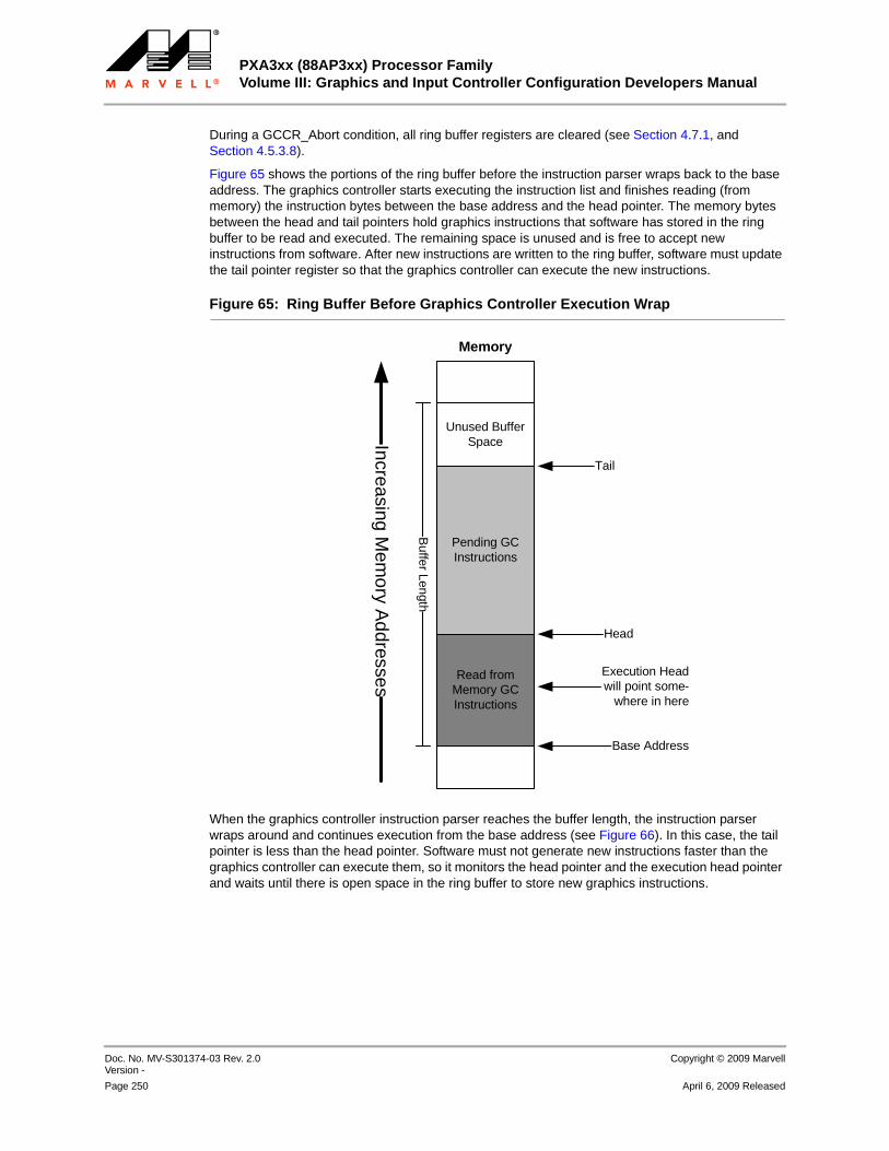
PXA3xx (88AP3xx) Processor FamilyVolume III: Graphics and Input Controller Configuration Developers Manual
Doc. No. MV-S301374-03 Rev. 2.0 Version -
Copyright © 2009 Marvell
Page 250 April 6, 2009 Released
12345678910111213141516171819202122232425262728293031323334353637383940414243444546474849505152535455565758
During a GCCR_Abort condition, all ring buffer registers are cleared (see Section 4.7.1, and Section 4.5.3.8).
Figure 65 shows the portions of the ring buffer before the instruction parser wraps back to the base address. The graphics controller starts executing the instruction list and finishes reading (from memory) the instruction bytes between the base address and the head pointer. The memory bytes between the head and tail pointers hold graphics instructions that software has stored in the ring buffer to be read and executed. The remaining space is unused and is free to accept new instructions from software. After new instructions are written to the ring buffer, software must update the tail pointer register so that the graphics controller can execute the new instructions.
Figure 65: Ring Buffer Before Graphics Controller Execution Wrap
When the graphics controller instruction parser reaches the buffer length, the instruction parser wraps around and continues execution from the base address (see Figure 66). In this case, the tail pointer is less than the head pointer. Software must not generate new instructions faster than the graphics controller can execute them, so it monitors the head pointer and the execution head pointer and waits until there is open space in the ring buffer to store new graphics instructions.
Pending GC Instructions
Memory
Tail
Head
Read from Memory GC Instructions
Execution Headwill point some-
where in here
Buffer Length
Unused Buffer Space
Base Address
Increasing Mem
ory Addresses

Graphics ControllerFunctional Description
Copyright © 2009 Marvell Doc. No. MV-S301374-03 Rev. 2.0Version -
April 6, 2009 Released Page 251
12345678910111213141516171819202122232425262728293031323334353637383940414243444546474849505152535455565758
Figure 66: Ring Buffer After Graphics Controller Execution Wrap
The ring buffer can also be used in an alternating double-buffer implementation with one memory space for executing graphics instructions and an alternate memory space for generating graphics instructions. In this double-buffer implementation, software does not have to manage the head pointer and tail pointer registers in real time. Figure 67 shows how the graphics controller executes from a start pointer in lower memory while software generates instructions for the next graphics frame in the memory space above the ring buffer (left side of the figure). When the current frame (N) is complete and committed to the display front buffer so that the head pointer equals the tail pointer, software programs the base address, length, and tail pointer values, respectively, for the alternate ring buffer into the ring buffer registers. Software must be sure to follow the correct order for programming these (for the next frame (N + 1). While the graphics controller executes frame N + 1, the N+2 frame can be generated and stored in the ring buffer previously used for the graphics instruction list of frame N.
This technique can be used to implement alternating triple-buffer graphics instruction lists (frames). The first list can be in execution, the second list can be pending execution, and the third list can be in generation. Again, the ring buffer registers should not be reprogrammed until the Execution Head Pointer register is equal to the Tail Pointer register, signifying that the graphics controller finished executing all instructions in the current ring buffer.
Pending GC Instructions
Memory
Tail
Head
Read from Memory GC Instructions
Execution Head will point some-
where in here
Buffer Length
Base Address
Increasing Mem
ory Addresses
Pending GC Instructions

PXA3xx (88AP3xx) Processor FamilyVolume III: Graphics and Input Controller Configuration Developers Manual
Doc. No. MV-S301374-03 Rev. 2.0 Version -
Copyright © 2009 Marvell
Page 252 April 6, 2009 Released
12345678910111213141516171819202122232425262728293031323334353637383940414243444546474849505152535455565758
Figure 67: Ring Buffer Double Buffered Implementation
4.5.5.3 Batch BuffersThe change of control flow from a ring buffer to a batch buffer is caused by a Batch Buffer Start instruction in the batch buffer (see Figure 68). The change of control flow from a batch buffer back to a ring buffer is caused by a Batch Buffer End instruction in the batch buffer (see Figure 68). Change of control flow from one batch buffer to another is caused by a Batch Buffer Start instruction in the current batch buffer (see Figure 69). Details on the Batch Buffer Start and Batch Buffer End instructions are provided in Section 4.6.1.1 and Section 4.6.1.2, respectively. For the current batch buffer, the graphics controller maintains the base, head, and execution head read-only registers. Upon receipt of a Batch Buffer Start instruction, the graphics controller loads these three registers with the base address of a batch buffer.
If the last graphics instruction in the ring buffer is a batch Buffer Start instruction, the Execution End of Buffer interrupt request is generated while instruction execution continues in the batch buffer. If this behavior is not desired, the last instruction in the ring buffer must not be a Batch Buffer Start instruction; it can be some padding instruction such as a NOP instruction (see Figure 70).
Pending GC Instructions(frame n+1)
Memory
Tail
HeadRead from
Memory GC Instructions
Execution Head will point some-
where in here
Buffer Length
Base Address
Increasing Mem
ory Addresses
Pending GC Instructions(frame n)
Unused Buffer Space
Unused Buffer Space
Pending GC Instructions(frame n+1)
Memory
Tail
Head
Read from Memory GC Instructions
Execution Head will point some-
where in hereB
uffer Length
Base Address
Pending GC Instructions(frame n+2)
Unused Buffer Space
Unused Buffer Space
Before frame n
completes
After frame n
completes

Graphics ControllerFunctional Description
Copyright © 2009 Marvell Doc. No. MV-S301374-03 Rev. 2.0Version -
April 6, 2009 Released Page 253
12345678910111213141516171819202122232425262728293031323334353637383940414243444546474849505152535455565758
Figure 68: Basic Batch Buffer Call
Pending GC Instructions
Ring Buffer
Tail
Head
Completed GC Instructions
Buffer Length
Base Address
Increasing Mem
ory Addresses Batch Buffer START
Unused Buffer Space
Batch Buffer END TAIL
BASE
Batch Buffer 0
2. Transfer execution from Batch Buffer 0 back to Ring Buffer here
1. Transfer execution from Ring Buffer to Batch Buffer 0 here

PXA3xx (88AP3xx) Processor FamilyVolume III: Graphics and Input Controller Configuration Developers Manual
Doc. No. MV-S301374-03 Rev. 2.0 Version -
Copyright © 2009 Marvell
Page 254 April 6, 2009 Released
12345678910111213141516171819202122232425262728293031323334353637383940414243444546474849505152535455565758
Figure 69: Chained Batch Buffer Call
Pending GC Instructions
Ring Buffer
Tail
Head
Completed GC Instructions
Buffer Length
Base Address
Increasing Mem
ory Addresses Batch Buffer START
Unused Buffer Space
Batch Buffer START TAIL
BASE
Batch Buffer 0
Batch Buffer END TAIL
BASE
Batch Buffer 1
1. Transfer execution from Ring
Buffer to Batch Buffer 0 here
3. Transfer execution from
Batch Buffer 1 back to Ring Buffer here
2. Transfer execution from
Batch Buffer 0 to Batch Buffer 1 here

Graphics ControllerFunctional Description
Copyright © 2009 Marvell Doc. No. MV-S301374-03 Rev. 2.0Version -
April 6, 2009 Released Page 255
12345678910111213141516171819202122232425262728293031323334353637383940414243444546474849505152535455565758
Figure 70: End of Buffer Interrupt Generation During Batch Buffer Execution
4.5.5.4 Display Front and Back BuffersThe graphics controller can render pixels into either the destination 0 or the destination 1 buffer using the respective Graphics Controller Destination x Base Address register (GCDxBR). In a double-buffered implementation, the destination buffers are coordinated with the LCD controller so that the graphics controller renders pixels into the display back buffer (initially the destination 1 buffer) while the LCD controller refreshes the display panel from the display front buffer (initially the destination 0 buffer). The Buffer Flip instruction notifies the graphics controller about when to change (flip) its rendering of pixels (pixel Writes) to the opposite destination buffer.
4.5.6 Graphics Instruction ListThe graphics controller executes control and memory interface instructions to control the graphics controller and to control access to the ring and batch buffers and the control registers. The graphics controller executes 2-D graphics instructions to perform pixel rendering. Table 129 and Table 130 provide an overview of the instructions.
Ring Buffer Tail
Completed GC Instructions
Buffer Length
Base Address
Increasing Mem
ory Addresses
Batch Buffer START Batch Buffer END TAIL
BASE
Batch Buffer 0
1. Transfer execution from Ring Buffer to Batch Buffer 0
here
3. Transfer execution from Batch Buffer 0 back
to Ring Buffer here
2. Execution End of Buffer interrupt gets generated here
Instructions are still being executed inside the Batch Buffer

PXA3xx (88AP3xx) Processor FamilyVolume III: Graphics and Input Controller Configuration Developers Manual
Doc. No. MV-S301374-03 Rev. 2.0 Version -
Copyright © 2009 Marvell
Page 256 April 6, 2009 Released
12345678910111213141516171819202122232425262728293031323334353637383940414243444546474849505152535455565758
Table 129: Graphics Controller Control and Memory Interface Instructions
Instruct ion Descript ion
Batch Buffer Start Directs the graphics controller to fetch the next instruction from a batch buffer. Can be used to transfer instruction fetching either from the ring buffer to a batch buffer or from one batch buffer to another.
Batch Buffer End Directs the graphics controller to fetch the next instruction from the next ring buffer location after the location containing the Batch Buffer Start instruction.
Buffer Info Provides addresses, pixel format, and display size information to the graphics controller for all source and destination buffers.
Load Register Loads a pixel ALU scratch register from memory or immediate.
NOP No graphics operation. Can be used to pad an instruction stream. Carries an identifier that is stored in the NOP Status register.
Destination Buffer Flip Flips (swaps) the destination buffers (display front buffer and display back buffer).
Store Register Stores the data in a Pixel ALU scratch register to memory.
Interrupt Generates a graphics controller interrupt request.
Wait for Event Stalls the graphics controller until the event occurs (for example, LCD controller or QCI controller input synchronization signals and a register read or Write).
Table 130: Graphics Controller 2-D Graphics Instructions
Instruct ion Descript ion
Color Fill Fills the destination rectangle with the specified color.
Chroma Key BLT Replaces the destination with a source if the destination value is greater than a specific threshold value. The logical operation can also be inverted.
Line Draw Draws a line of a programmable width.
Anti-aliased Line Draw Draws an anti-aliased line of a programmable width. Based on a pre-rasterized line cross section.
Stretch BLT Copies source to destination, enlarging a block using a bilinear interpolation.
Decimate BLT Copies source to destination, reducing a block using a bilinear decimation.
Alpha Blend BLT Combines two rectangular blocks using a supplied factor or factor array.
Scale BLT Multiplies source pixels by scale factor or factor array.
Bias BLT Adds (or subtracts) factor to source.
Pattern Fill BLT Fills a destination area with a source pattern.

Graphics ControllerFunctional Description
Copyright © 2009 Marvell Doc. No. MV-S301374-03 Rev. 2.0Version -
April 6, 2009 Released Page 257
12345678910111213141516171819202122232425262728293031323334353637383940414243444546474849505152535455565758
4.5.7 Pixel Data FormatsThe pixel ALU processes pixel formats ranging from 8 bits per pixel (for example, Lookup Table Index format) to 64 bits per pixel (for example, 16 bits red, 16 bits green, 16 bits blue, plus 16 bits alpha). Each pixel occupies a specific number of bytes, including reserved space, that is called a step size. With the exception of the Lookup Table Index format, the color representation is that of generic RGB data, where each color represents an arbitrary primary color intensity value. The Lookup Table Index format is simply an 8-bit index that points to a location in a lookup table containing an RGB color value. The value of the RGB color represents the perceived brightness as defined for a typical human observer. All pixel formats and processing operations are designed to be perceived as linear, given a linear operation. For example, if the pixel data value is halved, the displayed result is to be perceived as half brightness. This has a constraining effect on the gamma function of the display.
The Illegal Pixel Format/Step Size Interrupt request is generated if a reserved pixel format is programmed, there is an attempt to use a reserved format, or the step size does not match the programmed pixel format. In cases where the latter happens:
1. The pixel format has precedence over the step size 2. The step size is set to a compatible value
3. An interrupt request is generated, and 4. The graphics controller continues operation.
See Section 4.5.2.1 for more information.
Rotate BLT Rotates BLT output by some rotation factor.
Raster Operation BLT Performs any of 256 raster operations on a BLT.
Table 130: Graphics Controller 2-D Graphics Instructions (Continued)
Instruct ion Descript ion
Table 131: Standard RGB Pixel Data Formats
Bits per Pixel
Format ID Value(GCDxPF[PFORM])
RGB Format Valid Step Sizes
Supported in LCD Control ler
Supported in QCI Control ler
8 bit 0b0000 Lookup Table Index 1 YES NO
15 bit 0b0001 RGB 5:5:5 2 NO NO
16 bit 0b0010 RGBT 5:5:5:1 2 YES NO
16 bit 0b0011 RGB 5:6:5 2 YES NO
18 bit 0b0100 RGB 6:6:6 3, 4 YES NO
19 bit 0b0101 RGBT 6:6:6:1 3, 4 YES NO
24 bit 0b0110 RGB 8:8:8 3, 4 4 bytes only 4 bytes only
24 bit 0b0111 RGBA 6:6:6:6 3, 4 4 bytes only NO
25 bit 0b1000 RGBT 8:8:8:1 4 YES NO
32 bit 0b1001 RGBA 8:8:8:8 4 NO NO

PXA3xx (88AP3xx) Processor FamilyVolume III: Graphics and Input Controller Configuration Developers Manual
Doc. No. MV-S301374-03 Rev. 2.0 Version -
Copyright © 2009 Marvell
Page 258 April 6, 2009 Released
12345678910111213141516171819202122232425262728293031323334353637383940414243444546474849505152535455565758
4.5.7.1 Pixel Data Memory OrganizationTable 132 shows the packed and unpacked memory storage for all pixel formats. The step sizes are shown for each pixel format. Step size is defined as the number of bytes per pixel in memory. The step sizes shown, for both packed and unpacked storage, are the only allowable sizes. If a step size does not match a pixel format, compatible step size is forced (see the bottom row of Table 131).
The graphics controller manages many of the pixel formats managed by the LCD controller. Software must coordinate the destination buffer pixel type with that of the display buffers for the LCD controller if the destination buffer is used for display purposes. For details on display buffer pixel data organization, see the LCD Controller chapter.
48 bit 0b1010 RGB 16:16:16 8 NO NO
64 bit 0b1011 RGBA 16:16:16:16 8 NO NO
— 0b1100 – 0b1111 Reserved Causes the Illegal Pixel Format interrupt request to be generated. See Section 4.5.2.1. If any reserved pixel formats are programmed, the pixel format is forced to 64-bit RGBA 16:16:16:16.
Table 131: Standard RGB Pixel Data Formats (Continued)
Bits per Pixel
Format ID Value(GCDxPF[PFORM])
RGB Format Valid Step Sizes
Supported in LCD Control ler
Supported in QCI Control ler
Table 132: 8-Bit Lookup Table Index Packed Pixel Storage (Optimum Step Size = 1 byte)
Bit 31 30 29 28 27 26 25 24 23 22 21 20 19 18 17 16 15 14 13 12 11 10 9 8 7 6 5 4 3 2 1 0
0x0 Pixel 3 Pixel 2 Pixel 1 Pixel 0
0x4 Pixel 7 Pixel 6 Pixel 5 Pixel 4
Table 133: 15-Bit RGB 5:5:5 Packed Pixel Storage (Optimum Step Size = 2 bytes)
Bit 31 30 29 28 27 26 25 24 23 22 21 20 19 18 17 16 15 14 13 12 11 10 9 8 7 6 5 4 3 2 1 0
0x0
Res
erve
d
Red 1 Green 1 Blue 1
Res
erve
d
Red 0 Green 0 Blue 0
0x4
Res
erve
d
Red 3 Green 3 Blue 3
Res
erve
d
Red 2 Green 2 Blue 2
Table 134: 16-Bit RGBT 5:5:5:1 Packed Pixel Storage (Optimum Step Size = 2 bytes)
Bit 31 30 29 28 27 26 25 24 23 22 21 20 19 18 17 16 15 14 13 12 11 10 9 8 7 6 5 4 3 2 1 0
0x0 T Red 1 Green 1 Blue 1 T Red 0 Green 0 Blue 0
0x4 T Red 3 Green 3 Blue 3 T Red 2 Green 2 Blue 2

Graphics ControllerFunctional Description
Copyright © 2009 Marvell Doc. No. MV-S301374-03 Rev. 2.0Version -
April 6, 2009 Released Page 259
12345678910111213141516171819202122232425262728293031323334353637383940414243444546474849505152535455565758
Table 135: 16-Bit RGB 5:6:5 Packed Pixel Storage (Optimum Step Size = 2 bytes)
Bit 31 30 29 28 27 26 25 24 23 22 21 20 19 18 17 16 15 14 13 12 11 10 9 8 7 6 5 4 3 2 1 0
0x0 Red 1 Green 1 Blue 1 Red 0 Green 0 Blue 0
0x4 Red 3 Green 3 Blue 3 Red 2 Green 2 Blue 2
Table 136: 18-Bit RGB 6:6:6 Unpacked Pixel Storage (Step Size = 4 bytes)
Bit 31 30 29 28 27 26 25 24 23 22 21 20 19 18 17 16 15 14 13 12 11 10 9 8 7 6 5 4 3 2 1 0
0x0 Reserved Reserved Red 0 Green 0 Blue 0
0x4 Reserved Reserved Red 1 Green 1 Blue 1
Table 137: 18-Bit RGB 6:6:6 Packed Pixel Storage (Optimum Step Size = 3 bytes)
Bit 31 30 29 28 27 26 25 24 23 22 21 20 19 18 17 16 15 14 13 12 11 10 9 8 7 6 5 4 3 2 1 0
0x0 Green 1 [1:0]
Blue 1 Reserved Red 0 Green 0 Blue 0
0x4 Red 2 [3:0]
Green 2 Blue 2 Reserved Red 1 Green 1[5:2]
0x8 Reserved Red 3 Green 3 Blue 3 Reserved Red 2 [5:4]
Table 138: 19-Bit RGBT 6:6:6 Unpacked Pixel Storage (Step Size = 4 bytes)
Bit 31 30 29 28 27 26 25 24 23 22 21 20 19 18 17 16 15 14 13 12 11 10 9 8 7 6 5 4 3 2 1 0
0x0 Reserved Reserved T Red 0 Green 0 Blue 0
0x4 Reserved Reserved T Red 1 Green 1 Blue 1
Table 139: 19-Bit RGBT 6:6:6 Packed Pixel Storage (Optimum Step Size = 3 bytes)
Bit 31 30 29 28 27 26 25 24 23 22 21 20 19 18 17 16 15 14 13 12 11 10 9 8 7 6 5 4 3 2 1 0
0x0 Green 1 [1:0]
Blue 1 Reserved T Red 0 Green 0 Blue 0
0x4 Red 2 [3:0]
Green 2 Blue 2 Reserved T Red 1 Green 1[5:2]
0x8 Reserved T Red 3 Green 3 Blue 3 Reserved T Red 2 [5:4]

PXA3xx (88AP3xx) Processor FamilyVolume III: Graphics and Input Controller Configuration Developers Manual
Doc. No. MV-S301374-03 Rev. 2.0 Version -
Copyright © 2009 Marvell
Page 260 April 6, 2009 Released
12345678910111213141516171819202122232425262728293031323334353637383940414243444546474849505152535455565758
Table 140: 24-Bit RGB 8:8:8 Unpacked Pixel Storage (Step Size = 4 bytes)
Bit 31 30 29 28 27 26 25 24 23 22 21 20 19 18 17 16 15 14 13 12 11 10 9 8 7 6 5 4 3 2 1 0
0x0 Reserved Red 0 Green 0 Blue 0
0x4 Reserved Red 1 Green 1 Blue 1
Table 141: 24-Bit RGB 8:8:8 Packed Pixel Storage (Optimum Step Size = 3 bytes)
Bit 31 30 29 28 27 26 25 24 23 22 21 20 19 18 17 16 15 14 13 12 11 10 9 8 7 6 5 4 3 2 1 0
0x0 Blue 1 Red 0 Green 0 Blue 0
0x4 Green 2 Blue 2 Red 1 Green 1
0x8 Red 3 Green 3 Blue 3 Red 2
Table 142: 24-Bit RGBA 6:6:6:6 Unpacked Pixel Storage (Step Size = 4 bytes)
Bit 31 30 29 28 27 26 25 24 23 22 21 20 19 18 17 16 15 14 13 12 11 10 9 8 7 6 5 4 3 2 1 0
0x0 Reserved Alpha 0 Red 0 Green 0 Blue 0
0x4 Reserved Alpha 1 Red 1 Green 1 Blue 1
Table 143: 24-Bit RGBA 6:6:6:6 Packed Pixel Storage (Optimum Step Size = 3 bytes)
Bit 31 30 29 28 27 26 25 24 23 22 21 20 19 18 17 16 15 14 13 12 11 10 9 8 7 6 5 4 3 2 1 0
0x0 Green 1 [1:0]
Blue 1 Alpha 0 Red 0 Green 0 Blue 0
0x4 Red 2 [3:0]
Green 2 Blue 2 Alpha 1 Red 1 Green 1[5:2]
0x8 Alpha 3 Red 3 Green 3 Blue 3 Alpha 2 Red 2 [5:4]
Table 144: 25-Bit RGBT 8:8:8:1 Unpacked Pixel Storage (Step Size = 4 bytes)
Bit 31 30 29 28 27 26 25 24 23 22 21 20 19 18 17 16 15 14 13 12 11 10 9 8 7 6 5 4 3 2 1 0
0x0 Reserved T Red 0 Green 0 Blue 0
0x4 Reserved T Red 1 Green 1 Blue 1

Graphics ControllerFunctional Description
Copyright © 2009 Marvell Doc. No. MV-S301374-03 Rev. 2.0Version -
April 6, 2009 Released Page 261
12345678910111213141516171819202122232425262728293031323334353637383940414243444546474849505152535455565758
4.5.7.2 Pixel Type ConversionThe graphics controller performs all of its operations on 64-bit pixels in the RGBA 16:16:16:16 pixel format. All input source pixels must be converted up to the RGBA 16:16:16:16 pixel format, and all rendered pixels must be converted down from RGBA 16:16:16:16 pixel format before they are stored to the current destination buffer. Table 150 through Table 161 show all conversions up to the RGBA 16:16:16:16 pixel format, and Table 162 through Table 173 show all conversions down from the RGBA 16:16:16:16 pixel format. For all conversion examples except the LSB of each input color value, fully saturated pixels are used as the inputs. The lowest color bit is extended when converting up to the RGBA 16:16:16:16 pixel format; this is shown in the table as value A, R, G, and B (for alpha, red, green, and blue LSB).
Rules for converting between RGB and RGBA are as follows:
If the input pixel format is RGBA and the output pixel format is RGB, the alpha value on the incoming pixels is ignored.
If the output pixel format is RGBA and the input operand is RGB pixel format, then the GCALPHASET register must contain a valid alpha value, which the graphics controller will use to update the output content. If the GCALPHASET register does not indicate any valid alpha value, the output alpha will be 0b0. See Section 4.7.5.
Rules for converting between RGBA and RGBT are as follows:
If the input pixel format is RGBA and the output pixel format is RGBT, the GCTSET register should contain a valid transparency value that the graphics controller uses to update the output content. If GCTSET does not, the output transparency follows Table 149. See Section 4.7.6.
Table 145: 32-Bit RGBA 8:8:8:8 Packed Pixel Storage (Optimum Step Size = 4 bytes)
Bit 31 30 29 28 27 26 25 24 23 22 21 20 19 18 17 16 15 14 13 12 11 10 9 8 7 6 5 4 3 2 1 0
0x0 Alpha 0 Red 0 Green 0 Blue 0
0x4 Alpha 1 Red 1 Green 1 Blue 1
Table 146: 48-Bit RGB 16:16:16 Unpacked Pixel Storage (Step Size = 8 bytes)
Bit 31 30 29 28 27 26 25 24 23 22 21 20 19 18 17 16 15 14 13 12 11 10 9 8 7 6 5 4 3 2 1 0
0x0 Green 0 Blue 0
0x4 Reserved Red 0
0x8 Green 1 Blue 1
0xC Reserved Red 1
Table 147: 64-Bit RGBA 16:16:16:16 Packed Pixel Storage (Optimum Step Size = 8 bytes)
Bit 31 30 29 28 27 26 25 24 23 22 21 20 19 18 17 16 15 14 13 12 11 10 9 8 7 6 5 4 3 2 1 0
0x0 Green 0 Blue 0
0x4 Alpha 0 Red 0
0x8 Green 1 Blue 1
0xC Alpha 1 Red 1

PXA3xx (88AP3xx) Processor FamilyVolume III: Graphics and Input Controller Configuration Developers Manual
Doc. No. MV-S301374-03 Rev. 2.0 Version -
Copyright © 2009 Marvell
Page 262 April 6, 2009 Released
12345678910111213141516171819202122232425262728293031323334353637383940414243444546474849505152535455565758
If the output pixel format is RGBA and the input operand is of RGBT pixel format, the GCALPHASET register must contain a valid alpha value that the graphics controller uses to update the output content. If the GCALPHASET register does not contain a valid alpha value, the output alpha follows Table 148.
Table 148: Transparency to Alpha Conversion
Input T Value Result ing Alpha Value
0 0xFFFF
1 0x0000
Table 149: Alpha to Transparency Conversion
Input Alpha-Value Result ing T-Value
0x0000 – 0x7FFF 1
0x8000 – 8xFFFF 0
Table 150: Conversion from 8-Bit Lookup Table Index to RGBA 16:16:16:16
Convert From: 8-bit Lookup Table Index
Bit
31
30
29
28
27
26
25
24
23
22
21
20
19
18
17
16
15
14
13
12
11
10
9 8 7 6 5 4 3 2 1 0
0x
0
NA
B7
B6
B5
B4
B3
B2
B1
B0
Convert To: 64-bit RGBA 16:16:16:16
Bit
31
30
29
28
27
26
25
24
23
22
21
20
19
18
17
16
15
14
13
12
11
10
9 8 7 6 5 4 3 2 1 0
0x
0
0 0 0 0 0 0 0 0 0 0 0 0 0 0 0 0 B7
B6
B5
B4
B3
B2
B1
B0
B0
B0
B0
B0
B0
B0
B0
B0
0x
4
* * * * * * * * * * * * * * * * 0 0 0 0 0 0 0 0 0 0 0 0 0 0 0 0* Alpha value is updated based on programming in the GCALPHASET registers.
Table 151: Conversion from 15-Bit RGB 5:5:5 to RGBA 16:16:16:16
Convert From: 15-bit RGB 5:5:5
Bit 31 30 29 28 27 26 25 24 23 22 21 20 19 18 17 16 15 14 13 12 11 10 9 8 7 6 5 4 3 2 1 0
0x0 NA R4 R3 R2 R1 R0 G4 G3 G2 G1 G0 B4 B3 B2 B1 B0
Convert To: 64-bit RGBA 16:16:16:16
Bit 31 30 29 28 27 26 25 24 23 22 21 20 19 18 17 16 15 14 13 12 11 10 9 8 7 6 5 4 3 2 1 0
0x0 G4 G3 G2 G1 G0 G0 G0 G0 G0 G0 G0 G0 G0 G0 G0 G0 B4 B3 B2 B1 B0 B0 B0 B0 B0 B0 B0 B0 B0 B0 B0 B0

Graphics ControllerFunctional Description
Copyright © 2009 Marvell Doc. No. MV-S301374-03 Rev. 2.0Version -
April 6, 2009 Released Page 263
12345678910111213141516171819202122232425262728293031323334353637383940414243444546474849505152535455565758
0x4 * * * * * * * * * * * * * * * * R4 R3 R2 R1 R0 R0 R0 R0 R0 R0 R0 R0 R0 R0 R0 R0
* Alpha value is updated based on programming in the GCALPHASET registers. See Section 4.7.5
Table 151: Conversion from 15-Bit RGB 5:5:5 to RGBA 16:16:16:16 (Continued)
Convert From: 15-bit RGB 5:5:5
Bit 31 30 29 28 27 26 25 24 23 22 21 20 19 18 17 16 15 14 13 12 11 10 9 8 7 6 5 4 3 2 1 0
0x0 NA R4 R3 R2 R1 R0 G4 G3 G2 G1 G0 B4 B3 B2 B1 B0
Convert To: 64-bit RGBA 16:16:16:16
Bit 31 30 29 28 27 26 25 24 23 22 21 20 19 18 17 16 15 14 13 12 11 10 9 8 7 6 5 4 3 2 1 0
Table 152: Conversion from 16-Bit RGBT 5:5:5:1 to RGBA 16:16:16:16
Convert From: 16-bit RGBT 5:5:5:1
Bit 31 30 29 28 27 26 25 24 23 22 21 20 19 18 17 16 15 14 13 12 11 10 9 8 7 6 5 4 3 2 1 0
0x0 NA 1 R4 R3 R2 R1 R0 G4 G3 G2 G1 G0 B4 B3 B2 B1 B0
Convert To: 64-bit RGBA 16:16:16:16
Bit 31 30 29 28 27 26 25 24 23 22 21 20 19 18 17 16 15 14 13 12 11 10 9 8 7 6 5 4 3 2 1 0
0x0 G4 G3 G2 G1 G0 G0 G0 G0 G0 G0 G0 G0 G0 G0 G0 G0 B4 B3 B2 B1 B0 B0 B0 B0 B0 B0 B0 B0 B0 B0 B0 B0
0x4 * * * * * * * * * * * * * * * * R4 R3 R2 R1 R0 R0 R0 R0 R0 R0 R0 R0 R0 R0 R0 R0
* Alpha value is updated based on programming in the GCALPHASET registers. Section 4.7.5
Table 153: Conversion from 16-Bit RGB 5:6:5 to RGBA 16:16:16:16
Convert From: 16-bit RGB 5:6:5
Bit 31 30 29 28 27 26 25 24 23 22 21 20 19 18 17 16 15 14 13 12 11 10 9 8 7 6 5 4 3 2 1 0
0x0 NA R4 R3 R2 R1 R0 G5 G4 G3 G2 G1 G0 B4 B3 B2 B1 B0
Convert To: 64-bit RGBA 16:16:16:16
Bit 31 30 29 28 27 26 25 24 23 22 21 20 19 18 17 16 15 14 13 12 11 10 9 8 7 6 5 4 3 2 1 0
0x0 G5 G4 G3 G2 G1 G0 G0 G0 G0 G0 G0 G0 G0 G0 G0 G0 B4 B3 B2 B1 B0 B0 B0 B0 B0 B0 B0 B0 B0 B0 B0 B0
0x4 * * * * * * * * * * * * * * * * R4 R3 R2 R1 R0 R0 R0 R0 R0 R0 R0 R0 R0 R0 R0 R0
* Alpha value is updated based on programming in the GCALPHASET registers. See Section 4.7.5

PXA3xx (88AP3xx) Processor FamilyVolume III: Graphics and Input Controller Configuration Developers Manual
Doc. No. MV-S301374-03 Rev. 2.0 Version -
Copyright © 2009 Marvell
Page 264 April 6, 2009 Released
12345678910111213141516171819202122232425262728293031323334353637383940414243444546474849505152535455565758
Table 154: Conversion from 18-Bit RGB 6:6:6 to RGBA 16:16:16:16
Convert From: 18-bit RGB 6;6:6
Bit 31 30 29 28 27 26 25 24 23 22 21 20 19 18 17 16 15 14 13 12 11 10 9 8 7 6 5 4 3 2 1 0
0x0 NA R5 R4 R3 R2 R1 R0 G5 G4 G3 G2 G1 G0 B5 B4 B3 B2 B1 B0
Convert To: 64-bit RGBA 16:16:16:16
Bit 31 30 29 28 27 26 25 24 23 22 21 20 19 18 17 16 15 14 13 12 11 10 9 8 7 6 5 4 3 2 1 0
0x0 G5 G4 G3 G2 G1 G0 G0 G0 G0 G0 G0 G0 G0 G0 G0 G0 B5 B4 B3 B2 B1 B0 B0 B0 B0 B0 B0 B0 B0 B0 B0 B0
0x4 * * * * * * * * * * * * * * * * R5 R4 R3 R2 R1 R0 R0 R0 R0 R0 R0 R0 R0 R0 R0 R0
* Alpha value is updated based on programming in the GCALPHASET registers. See Section 4.7.5
Table 155: Conversion from 19-Bit RGBT 6:6:6:1 to RGBA 16:16:16:16
Convert From: 19-bit RGBT 6;6:6:1
Bit 31 30 29 28 27 26 25 24 23 22 21 20 19 18 17 16 15 14 13 12 11 10 9 8 7 6 5 4 3 2 1 0
0x0 NA 1 R5 R4 R3 R2 R1 R0 G5 G4 G3 G2 G1 G0 B5 B4 B3 B2 B1 B0
Convert To: 64-bit RGBA 16:16:16:16
Bit 31 30 29 28 27 26 25 24 23 22 21 20 19 18 17 16 15 14 13 12 11 10 9 8 7 6 5 4 3 2 1 0
0x0 G5 G4 G3 G2 G1 G0 G0 G0 G0 G0 G0 G0 G0 G0 G0 G0 B5 B4 B3 B2 B1 B0 B0 B0 B0 B0 B0 B0 B0 B0 B0 B0
0x4 * * * * * * * * * * * * * * * * R5 R4 R3 R2 R1 R0 R0 R0 R0 R0 R0 R0 R0 R0 R0 R0
* Alpha value is updated based on programming in the GCALPHASET registers. See Section 4.7.5
Table 156: Conversion from 24-Bit RGB 8:8:8 to RGBA 16:16:16:16
Convert From: 24-bit RGB 8:8:8
Bit 31 30 29 28 27 26 25 24 23 22 21 20 19 18 17 16 15 14 13 12 11 10 9 8 7 6 5 4 3 2 1 0
0x0 NA R7 R6 R5 R4 R3 R2 R1 R0 G7 G6 G5 G4 G3 G2 G1 G0 B7 B6 B5 B4 B3 B2 B1 B0
Convert To: 64-bit RGBA 16:16:16:16
Bit 31 30 29 28 27 26 25 24 23 22 21 20 19 18 17 16 15 14 13 12 11 10 9 8 7 6 5 4 3 2 1 0
0x0 G7 G6 G5 G4 G3 G2 G1 G0 G0 G0 G0 G0 G0 G0 G0 G0 B7 B6 B5 B4 B3 B2 B1 B0 B0 B0 B0 B0 B0 B0 B0 B0
0x4 * * * * * * * * * * * * * * * * R7 R6 R5 R4 R3 R2 R1 R0 R0 R0 R0 R0 R0 R0 R0 R0
* Alpha value is updated based on programming in the GCALPHASET registers. See Section 4.7.5

Graphics ControllerFunctional Description
Copyright © 2009 Marvell Doc. No. MV-S301374-03 Rev. 2.0Version -
April 6, 2009 Released Page 265
12345678910111213141516171819202122232425262728293031323334353637383940414243444546474849505152535455565758
Table 157: Conversion from 24-Bit RGBA 6:6:6:6 to RGBA 16:16:16:16
Convert From: 24-bit RGBA 6;6:6:6
Bit 31 30 29 28 27 26 25 24 23 22 21 20 19 18 17 16 15 14 13 12 11 10 9 8 7 6 5 4 3 2 1 0
0x0 NA A5 A4 A3 A2 A1 A0 R5 R4 R3 R2 R1 R0 G5 G4 G3 G2 G1 G0 B5 B4 B3 B2 B1 B0
Convert To: 64-bit RGBA 16:16:16:16
Bit 31 30 29 28 27 26 25 24 23 22 21 20 19 18 17 16 15 14 13 12 11 10 9 8 7 6 5 4 3 2 1 0
0x0 G5 G4 G3 G2 G1 G0 G0 G0 G0 G0 G0 G0 G0 G0 G0 G0 B5 B4 B3 B2 B1 B0 B0 B0 B0 B0 B0 B0 B0 B0 B0 B0
0x4 A5 A4 A3 A2 A1 A0 A0 A0 A0 A0 A0 A0 A0 A0 A0 A0 R5 R4 R3 R2 R1 R0 R0 R0 R0 R0 R0 R0 R0 R0 R0 R0
Table 158: Conversion from 25-Bit RGBT 8:8:8:1 to RGBA 16:16:16:16
Convert From: 25-bit RGBT 8:8:8:1
Bit 31 30 29 28 27 26 25 24 23 22 21 20 19 18 17 16 15 14 13 12 11 10 9 8 7 6 5 4 3 2 1 0
0x0 NA 1 R7 R6 R5 R4 R3 R2 R1 R0 G7 G6 G5 G4 G3 G2 G1 G0 B7 B6 B5 B4 B3 B2 B1 B0
Convert To: 64-bit RGBA 16:16:16:16
Bit 31 30 29 28 27 26 25 24 23 22 21 20 19 18 17 16 15 14 13 12 11 10 9 8 7 6 5 4 3 2 1 0
0x0 G7 G6 G5 G4 G3 G2 G1 G0 G0 G0 G0 G0 G0 G0 G0 G0 B7 B6 B5 B4 B3 B2 B1 B0 B0 B0 B0 B0 B0 B0 B0 B0
0x4 * * * * * * * * * * * * * * * * R7 R6 R5 R4 R3 R2 R1 R0 R0 R0 R0 R0 R0 R0 R0 R0
* Alpha value is updated based on programming in the GCALPHASET registers. See Section 4.7.5
Table 159: Conversion from 32-Bit RGBA 8:8:8:8 to RGBA 16:16:16:16
Convert From: 32-bit RGBA 8:8:8:8
Bit 31 30 29 28 27 26 25 24 23 22 21 20 19 18 17 16 15 14 13 12 11 10 9 8 7 6 5 4 3 2 1 0
0x0 A7 A6 A5 A4 A3 A2 A1 A0 R7 R6 R5 R4 R3 R2 R1 R0 G7 G6 G5 G4 G3 G2 G1 G0 B7 B6 B5 B4 B3 B2 B1 B0
Convert To: 64-bit RGBA 16:16:16:16
Bit 31 30 29 28 27 26 25 24 23 22 21 20 19 18 17 16 15 14 13 12 11 10 9 8 7 6 5 4 3 2 1 0
0x0 G7 G6 G5 G4 G3 G2 G1 G0 G0 G0 G0 G0 G0 G0 G0 G0 B7 B6 B5 B4 B3 B2 B1 B0 B0 B0 B0 B0 B0 B0 B0 B0
0x4 A7 A6 A5 A4 A3 A2 A1 A0 A0 A0 A0 A0 A0 A0 A0 A0 R7 R6 R5 R4 R3 R2 R1 R0 R0 R0 R0 R0 R0 R0 R0 R0

PXA3xx (88AP3xx) Processor FamilyVolume III: Graphics and Input Controller Configuration Developers Manual
Doc. No. MV-S301374-03 Rev. 2.0 Version -
Copyright © 2009 Marvell
Page 266 April 6, 2009 Released
12345678910111213141516171819202122232425262728293031323334353637383940414243444546474849505152535455565758
Table 160: Conversion from 48-Bit RGB 16:16:16 to RGBA 16:16:16:16
Convert From: 48-bit RGB 16:16:16
Bit 31 30 29 28 27 26 25 24 23 22 21 20 19 18 17 16 15 14 13 12 11 10 9 8 7 6 5 4 3 2 1 0
0x0 G15
G14
G13
G12
G11
G10
G9 G8 G7 G6 G5 G4 G3 G2 G1 G0 B15
B14
B13
B12
B11
B10
B9 B8 B7 B6 B5 B4 B3 B2 B1 B0
0x4 A15
A14
A13
A12
A11
A10
A9 A8 A7 A6 A5 A4 A3 A2 A1 A0 R15
R14
R13
R12
R11
R10
R9 R8 R7 R6 R5 R4 R3 R2 R1 R0
Convert To: 64-bit RGBA 16:16:16:16
Bit 31 30 29 28 27 26 25 24 23 22 21 20 19 18 17 16 15 14 13 12 11 10 9 8 7 6 5 4 3 2 1 0
0x0 G15
G14
G13
G12
G11
G10
G9 G8 G7 G6 G5 G4 G3 G2 G1 G0 B15
B14
B13
B12
B11
B10
B9 B8 B7 B6 B5 B4 B3 B2 B1 B0
0x4 * * * * * * * * * * * * * * * * R15
R14
R13
R12
R11
R10
R9 R8 R7 R6 R5 R4 R3 R2 R1 R0
* Alpha value is updated based on programming in the GCALPHASET registers. See Section 4.7.5
Table 161: Conversion from 64-Bit RGBA 16:16:16:16 to RGBA 16:16:16:16
Convert From: 64-bit RGBA 16:16:16:16
Bit 31 30 29 28 27 26 25 24 23 22 21 20 19 18 17 16 15 14 13 12 11 10 9 8 7 6 5 4 3 2 1 0
0x0 G15
G14
G13
G12
G11
G10
G9 G8 G7 G6 G5 G4 G3 G2 G1 G0 B15
B14
B13
B12
B11
B10
B9 B8 B7 B6 B5 B4 B3 B2 B1 B0
0x4 A15
A14
A13
A12
A11
A10
A9 A8 A7 A6 A5 A4 A3 A2 A1 A0 R15
R14
R13
R12
R11
R10
R9 R8 R7 R6 R5 R4 R3 R2 R1 R0
Convert To: 64-bit RGBA 16:16:16:16
Bit 31 30 29 28 27 26 25 24 23 22 21 20 19 18 17 16 15 14 13 12 11 10 9 8 7 6 5 4 3 2 1 0
0x0 G15
G14
G13
G12
G11
G10
G9 G8 G7 G6 G5 G4 G3 G2 G1 G0 B15
B14
B13
B12
B11
B10
B9 B8 B7 B6 B5 B4 B3 B2 B1 B0
0x4 A15
A14
A13
A12
A11
A10
A9 A8 A7 A6 A5 A4 A3 A2 A1 A0 R15
R14
R13
R12
R11
R10
R9 R8 R7 R6 R5 R4 R3 R2 R1 R0
Table 162: Conversion from RGBA 16:16:16:16 to 8-bit Lookup Table Index
Convert From: 64-bit RGBA 16:16:16:16
Bit 31 30 29 28 27 26 25 24 23 22 21 20 19 18 17 16 15 14 13 12 11 10 9 8 7 6 5 4 3 2 1 0
0x0 G15
G14
G13
G12
G11
G10
G9 G8 G7 G6 G5 G4 G3 G2 G1 G0 B15
B14
B13
B12
B11
B10
B9 B8 B7 B6 B5 B4 B3 B2 B1 B0
0x4 A15
A14
A13
A12
A11
A10
A9 A8 A7 A6 A5 A4 A3 A2 A1 A0 R15
R14
R13
R12
R11
R10
R9 R8 R7 R6 R5 R4 R3 R2 R1 R0
Convert To: 8-b it Lookup Table Index

Graphics ControllerFunctional Description
Copyright © 2009 Marvell Doc. No. MV-S301374-03 Rev. 2.0Version -
April 6, 2009 Released Page 267
12345678910111213141516171819202122232425262728293031323334353637383940414243444546474849505152535455565758
Bit 31 30 29 28 27 26 25 24 23 22 21 20 19 18 17 16 15 14 13 12 11 10 9 8 7 6 5 4 3 2 1 0
0x0 NA B15
B14
B13
B12
B11
B10
B9 B8
Table 162: Conversion from RGBA 16:16:16:16 to 8-bit Lookup Table Index (Continued)
Convert From: 64-bit RGBA 16:16:16:16
Bit 31 30 29 28 27 26 25 24 23 22 21 20 19 18 17 16 15 14 13 12 11 10 9 8 7 6 5 4 3 2 1 0
Table 163: Conversion from RGBA 16:16:16:16 to 15-bit RGB 5:5:5
Convert From: 64-bit RGBA 16:16:16:16
Bit 31 30 29 28 27 26 25 24 23 22 21 20 19 18 17 16 15 14 13 12 11 10 9 8 7 6 5 4 3 2 1 0
0x0 G15
G14
G13
G12
G11
G10
G9 G8 G7 G6 G5 G4 G3 G2 G1 G0 B15
B14
B13
B12
B11
B10
B9 B8 B7 B6 B5 B4 B3 B2 B1 B0
0x4 A15
A14
A13
A12
A11
A10
A9 A8 A7 A6 A5 A4 A3 A2 A1 A0 R15
R14
R13
R12
R11
R10
R9 R8 R7 R6 R5 R4 R3 R2 R1 R0
Convert To: 15-bit RGB 5:5:5
Bit 31 30 29 28 27 26 25 24 23 22 21 20 19 18 17 16 15 14 13 12 11 10 9 8 7 6 5 4 3 2 1 0
0x0 NA R15
R14
R13
R12
R11
G15
G14
G13
G12
G11
B15
B14
B13
B12
B11
Table 164: Conversion from RGBA 16:16:16:16 to 16-bit RGBT 5:5:5:1
Convert From: 64-bit RGBA 16:16:16:16
Bit 31 30 29 28 27 26 25 24 23 22 21 20 19 18 17 16 15 14 13 12 11 10 9 8 7 6 5 4 3 2 1 0
0x0 G15
G14
G13
G12
G11
G10
G9 G8 G7 G6 G5 G4 G3 G2 G1 G0 B15
B14
B13
B12
B11
B10
B9 B8 B7 B6 B5 B4 B3 B2 B1 B0
0x4 A15
A14
A13
A12
A11
A10
A9 A8 A7 A6 A5 A4 A3 A2 A1 A0 R15
R14
R13
R12
R11
R10
R9 R8 R7 R6 R5 R4 R3 R2 R1 R0
Convert To: 16-bit RGBT 5:5:5:1
Bit 31 30 29 28 27 26 25 24 23 22 21 20 19 18 17 16 15 14 13 12 11 10 9 8 7 6 5 4 3 2 1 0
0x0 NA * R15
R14
R13
R12
R11
G15
G14
G13
G12
G11
B15
B14
B13
B12
B11
* Transparency value is updated based on programming in the GCTSET registers. See Section 4.7.6

PXA3xx (88AP3xx) Processor FamilyVolume III: Graphics and Input Controller Configuration Developers Manual
Doc. No. MV-S301374-03 Rev. 2.0 Version -
Copyright © 2009 Marvell
Page 268 April 6, 2009 Released
12345678910111213141516171819202122232425262728293031323334353637383940414243444546474849505152535455565758
Table 165: Conversion from RGBA 16:16:16:16 to 16-bit RGB 5:6:5
Convert From: 64-bit RGBA 16:16:16:16
Bit 31 30 29 28 27 26 25 24 23 22 21 20 19 18 17 16 15 14 13 12 11 10 9 8 7 6 5 4 3 2 1 0
0x0 G15
G14
G13
G12
G11
G10
G9 G8 G7 G6 G5 G4 G3 G2 G1 G0 B15
B14
B13
B12
B11
B10
B9 B8 B7 B6 B5 B4 B3 B2 B1 B0
0x4 A15
A14
A13
A12
A11
A10
A9 A8 A7 A6 A5 A4 A3 A2 A1 A0 R15
R14
R13
R12
R11
R10
R9 R8 R7 R6 R5 R4 R3 R2 R1 R0
Convert To: 16-bit RGB 5:6:5
Bit 31 30 29 28 27 26 25 24 23 22 21 20 19 18 17 16 15 14 13 12 11 10 9 8 7 6 5 4 3 2 1 0
0x0 NA R15
R14
R13
R12
R11
G15
G14
G13
G12
G11
G10
B15
B14
B13
B12
B11
Table 166: Conversion from RGBA 16:16:16:16 to 18-bit RGB 6:6:6
Convert From: 64-bit RGBA 16:16:16:16
Bit 31 30 29 28 27 26 25 24 23 22 21 20 19 18 17 16 15 14 13 12 11 10 9 8 7 6 5 4 3 2 1 0
0x0 G15
G14
G13
G12
G11
G10
G9 G8 G7 G6 G5 G4 G3 G2 G1 G0 B15
B14
B13
B12
B11
B10
B9 B8 B7 B6 B5 B4 B3 B2 B1 B0
0x4 A15
A14
A13
A12
A11
A10
A9 A8 A7 A6 A5 A4 A3 A2 A1 A0 R15
R14
R13
R12
R11
R10
R9 R8 R7 R6 R5 R4 R3 R2 R1 R0
Convert To: 18-bit RGB 6:6:6
Bit 31 30 29 28 27 26 25 24 23 22 21 20 19 18 17 16 15 14 13 12 11 10 9 8 7 6 5 4 3 2 1 0
0x0 NA R15
R14
R13
R12
R11
R10
G15
G14
G13
G12
G11
G10
B15
B14
B13
B12
B11
B10
Table 167: Conversion from RGBA 16:16:16:16 to 19-bit RGBT 6:6:6:1
Convert From: 64-bit RGBA 16:16:16:16
Bit 31 30 29 28 27 26 25 24 23 22 21 20 19 18 17 16 15 14 13 12 11 10 9 8 7 6 5 4 3 2 1 0
0x0 G15
G14
G13
G12
G11
G10
G9 G8 G7 G6 G5 G4 G3 G2 G1 G0 B15
B14
B13
B12
B11
B10
B9 B8 B7 B6 B5 B4 B3 B2 B1 B0
0x4 A15
A14
A13
A12
A11
A10
A9 A8 A7 A6 A5 A4 A3 A2 A1 A0 R15
R14
R13
R12
R11
R10
R9 R8 R7 R6 R5 R4 R3 R2 R1 R0
Convert To: 19-bit RGBT 6:6:6:1
Bit 31 30 29 28 27 26 25 24 23 22 21 20 19 18 17 16 15 14 13 12 11 10 9 8 7 6 5 4 3 2 1 0
0x0 NA * R15
R14
R13
R12
R11
R10
G15
G14
G13
G12
G11
G10
B15
B14
B13
B12
B11
B10
* Transparency value is updated based on programming in the GCTSET registers. See Section 4.7.6

Graphics ControllerFunctional Description
Copyright © 2009 Marvell Doc. No. MV-S301374-03 Rev. 2.0Version -
April 6, 2009 Released Page 269
12345678910111213141516171819202122232425262728293031323334353637383940414243444546474849505152535455565758
Table 168: Conversion from RGBA 16:16:16:16 to 24-bit RGB 8:8:8
Convert From: 64-bit RGBA 16:16:16:16
Bit 31 30 29 28 27 26 25 24 23 22 21 20 19 18 17 16 15 14 13 12 11 10 9 8 7 6 5 4 3 2 1 0
0x0 G15
G14
G13
G12
G11
G10
G9 G8 G7 G6 G5 G4 G3 G2 G1 G0 B15
B14
B13
B12
B11
B10
B9 B8 B7 B6 B5 B4 B3 B2 B1 B0
0x4 A15
A14
A13
A12
A11
A10
A9 A8 A7 A6 A5 A4 A3 A2 A1 A0 R15
R14
R13
R12
R11
R10
R9 R8 R7 R6 R5 R4 R3 R2 R1 R0
Convert To: 24-bit RGB 8:8:8
Bit 31 30 29 28 27 26 25 24 23 22 21 20 19 18 17 16 15 14 13 12 11 10 9 8 7 6 5 4 3 2 1 0
0x0 NA R15
R14
R13
R12
R11
R10
R9 R8 G15
G14
G13
G12
G11
G10
G9 G8 B15
B14
B13
B12
B11
B10
B9 B8
Table 169: Conversion from RGBA 16:16:16:16 to 24-bit RGBA 6:6:6:6
Convert From: 64-bit RGBA 16:16:16:16
Bit 31 30 29 28 27 26 25 24 23 22 21 20 19 18 17 16 15 14 13 12 11 10 9 8 7 6 5 4 3 2 1 0
0x0 G15
G14
G13
G12
G11
G10
G9 G8 G7 G6 G5 G4 G3 G2 G1 G0 B15
B14
B13
B12
B11
B10
B9 B8 B7 B6 B5 B4 B3 B2 B1 B0
0x4 A15
A14
A13
A12
A11
A10
A9 A8 A7 A6 A5 A4 A3 A2 A1 A0 R15
R14
R13
R12
R11
R10
R9 R8 R7 R6 R5 R4 R3 R2 R1 R0
Convert To: 24-bit RGBA 6:6:6:6
Bit 31 30 29 28 27 26 25 24 23 22 21 20 19 18 17 16 15 14 13 12 11 10 9 8 7 6 5 4 3 2 1 0
0x0 NA A15
A14
A13
A12
A11
A10
R15
R14
R13
R12
R11
R10
G15
G14
G13
G12
G11
G10
B15
B14
B13
B12
B11
B10
Table 170: Conversion from RGBA 16:16:16:16 to 25-bit RGBT 8:8:8:1
Convert From: 64-bit RGBA 16:16:16:16
Bit 31 30 29 28 27 26 25 24 23 22 21 20 19 18 17 16 15 14 13 12 11 10 9 8 7 6 5 4 3 2 1 0
0x0 G15
G14
G13
G12
G11
G10
G9 G8 G7 G6 G5 G4 G3 G2 G1 G0 B15
B14
B13
B12
B11
B10
B9 B8 B7 B6 B5 B4 B3 B2 B1 B0
0x4 A15
A14
A13
A12
A11
A10
A9 A8 A7 A6 A5 A4 A3 A2 A1 A0 R15
R14
R13
R12
R11
R10
R9 R8 R7 R6 R5 R4 R3 R2 R1 R0
Convert To: 25-bit RGBT 8:8:8:1
Bit 31 30 29 28 27 26 25 24 23 22 21 20 19 18 17 16 15 14 13 12 11 10 9 8 7 6 5 4 3 2 1 0
0x0 NA * R15
R14
R13
R12
R11
R10
R9 R8 G15
G14
G13
G12
G11
G10
G9 G8 B15
B14
B13
B12
B11
B10
B9 B8
* Transparency value is updated based on programming in the GCTSET registers. See Section 4.7.6

PXA3xx (88AP3xx) Processor FamilyVolume III: Graphics and Input Controller Configuration Developers Manual
Doc. No. MV-S301374-03 Rev. 2.0 Version -
Copyright © 2009 Marvell
Page 270 April 6, 2009 Released
12345678910111213141516171819202122232425262728293031323334353637383940414243444546474849505152535455565758
Table 171: Conversion from RGBA 16:16:16:16 to 32-bit RGBA 8:8:8:8
Convert From: 64-bit RGBA 16:16:16:16
Bit 31 30 29 28 27 26 25 24 23 22 21 20 19 18 17 16 15 14 13 12 11 10 9 8 7 6 5 4 3 2 1 0
0x0 G15
G14
G13
G12
G11
G10
G9 G8 G7 G6 G5 G4 G3 G2 G1 G0 B15
B14
B13
B12
B11
B10
B9 B8 B7 B6 B5 B4 B3 B2 B1 B0
0x4 A15
A14
A13
A12
A11
A10
A9 A8 A7 A6 A5 A4 A3 A2 A1 A0 R15
R14
R13
R12
R11
R10
R9 R8 R7 R6 R5 R4 R3 R2 R1 R0
Convert To: 32-bit RGBA 8:8:8:8
Bit 31 30 29 28 27 26 25 24 23 22 21 20 19 18 17 16 15 14 13 12 11 10 9 8 7 6 5 4 3 2 1 0
0x0 A15
A14
A13
A12
A11
A10
A9 A8 R15
R14
R13
R12
R11
R10
R9 R8 G15
G14
G13
G12
G11
G10
G9 G8 B15
B14
B13
B12
B11
B10
B9 B8
Table 172: Conversion from RGBA 16:16:16:16 to 48-bit RGB 16:16:16
Convert From: 64-bit RGBA 16:16:16:16
Bit 31 30 29 28 27 26 25 24 23 22 21 20 19 18 17 16 15 14 13 12 11 10 9 8 7 6 5 4 3 2 1 0
0x0 G15
G14
G13
G12
G11
G10
G9 G8 G7 G6 G5 G4 G3 G2 G1 G0 B15
B14
B13
B12
B11
B10
B9 B8 B7 B6 B5 B4 B3 B2 B1 B0
0x4 A15
A14
A13
A12
A11
A10
A9 A8 A7 A6 A5 A4 A3 A2 A1 A0 R15
R14
R13
R12
R11
R10
R9 R8 R7 R6 R5 R4 R3 R2 R1 R0
Convert To: 48-bit RGB 16:16:16
Bit 31 30 29 28 27 26 25 24 23 22 21 20 19 18 17 16 15 14 13 12 11 10 9 8 7 6 5 4 3 2 1 0
0x0 G15
G14
G13
G12
G11
G10
G9 G8 G7 G6 G5 G4 G3 G2 G1 G0 B15
B14
B13
B12
B11
B10
B9 B8 B7 B6 B5 B4 B3 B2 B1 B0
0x4 NA R15
R14
R13
R12
R11
R10
R9 R8 R7 R6 R5 R4 R3 R2 R1 R0
Table 173: Conversion from RGBA 16:16:16:16 to 64-bit RGBA 16:16:16:16
Convert From: 64-bit RGBA 16:16:16:16
Bit 31 30 29 28 27 26 25 24 23 22 21 20 19 18 17 16 15 14 13 12 11 10 9 8 7 6 5 4 3 2 1 0
0x0 G15
G14
G13
G12
G11
G10
G9 G8 G7 G6 G5 G4 G3 G2 G1 G0 B15
B14
B13
B12
B11
B10
B9 B8 B7 B6 B5 B4 B3 B2 B1 B0
0x4 A15
A14
A13
A12
A11
A10
A9 A8 A7 A6 A5 A4 A3 A2 A1 A0 R15
R14
R13
R12
R11
R10
R9 R8 R7 R6 R5 R4 R3 R2 R1 R0
Convert To: 64-bit RGAB 16:16:16:16
Bit 31 30 29 28 27 26 25 24 23 22 21 20 19 18 17 16 15 14 13 12 11 10 9 8 7 6 5 4 3 2 1 0
0x0 G15
G14
G13
G12
G11
G10
G9 G8 G7 G6 G5 G4 G3 G2 G1 G0 B15
B14
B13
B12
B11
B10
B9 B8 B7 B6 B5 B4 B3 B2 B1 B0
0x4 A15
A14
A13
A12
A11
A10
A9 A8 A7 A6 A5 A4 A3 A2 A1 A0 R15
R14
R13
R12
R11
R10
R9 R8 R7 R6 R5 R4 R3 R2 R1 R0

Graphics ControllerFunctional Description
Copyright © 2009 Marvell Doc. No. MV-S301374-03 Rev. 2.0Version -
April 6, 2009 Released Page 271
12345678910111213141516171819202122232425262728293031323334353637383940414243444546474849505152535455565758
4.5.8 2-D Address Generation2-D address generation uses the following conversion equation to translate the X-pixel and Y-pixel coordinates in pixel space into a 32-bit (word) physical address (see Figure 71):
Physical Pixel Address = Y_line * STRIDE + X_pixel * STEP + BASE
For both packed and unpacked pixel formats, the buffer offset associated with a coordinate in pixel space is calculated as follows:
1. Multiply the input pixel Y-line number by the value in the buffer STRIDE register.2. Add the product from step 1 to the input pixel X-pixel number multiplied by the value in the
buffer STEP register.
Figure 71: 2-D Address Generation Block Diagram
Example 2 and Example 3 present calculations for unpacked and packed 2-D pixel addresses. Assume the following information for both cases.
Pixel coordinate is x = 7, y = 5 and the starting pixel coordinate is x = 0, y = 0.32-bit BASE Address of Display is 0x2100_0000 (contains the rendered pixel value).
Display size = 24 pixels × 12 lines
Example 2. Unpacked Pixel Format Address Conversion
Find the starting address for an unpacked pixel format as follows:
STEP = Number of bytes per pixel
• = 64 bits per pixel
• = 8 bytes per pixel (stored value)
STRIDE = Number of bytes per line
• = 8 bytes per pixel × 24 pixel per line
• = 192 bytes per line (stored value)
(x = 7, y = 5) Pixel Address
• = BASE + (Y × STRIDE) + (X × STEP)
• = 0x2100_0000 + (5 × 192 bytes per line) + (7 × 8 bytes per pixel)
Y (line number)
STRIDE (bytes per line)
X (pixel number)
STEP (bytes per pixel)
BASE_BYTE_ADDR
PIXEL_BYTE_ADDR
ALU/ACC

PXA3xx (88AP3xx) Processor FamilyVolume III: Graphics and Input Controller Configuration Developers Manual
Doc. No. MV-S301374-03 Rev. 2.0 Version -
Copyright © 2009 Marvell
Page 272 April 6, 2009 Released
12345678910111213141516171819202122232425262728293031323334353637383940414243444546474849505152535455565758
• = 0x2100_0000 + 1016 bytes
• = 0x2100_03F8 (Starting Address of pixel)
Example 3. Packed Pixel Format Address Conversion
Find the starting address for a packed pixel format, as follows:
STEP = Number of bytes per pixel
• = 24 bits per pixel
• = 3 bytes per pixel (stored value)
STRIDE = Number of bytes per line
• = 3 bytes per pixel × 24 pixel per line
• = 72 bytes per line (stored value)
(x = 7, y = 5) Pixel Address
• = BASE + (Y × STRIDE) + (X × STEP)
• = 0x2100_0000 + (5 × 72 bytes per line) + (7 × 3 bytes per pixel)
• = 0x2100_0000 + 381 bytes
• = 0x2100_017D (starting address of pixel)
4.5.9 Reading Extra PixelsFor both the Stretch BLT and Decimate BLT instructions, extra pixels not directly used in calculations are read from memory. Software must ensure that these extra pixel Reads do not reach into invalid memory spaces.
For the Stretch and Decimate BLT instructions, one extra pixel per line and one extra line per block is read from the Source 0 buffer. For example, if the Source 0 block size is 8x8, the block size that is actually read from the Source 0 buffer (memory region) is 9x9.Double word Reads are always performed on pixel data. Pixels that straddle double word boundaries result in two double word Reads.
4.5.10 Color SaturationIn saturating arithmetic, if a result cannot be fully represented in modulo 2n, the result is saturated to the largest or smallest possible value for modulo 2n. For unsigned saturation of the color values, the largest possible saturated value in the graphics controller is 2n and the smallest possible saturated value is 0. There are few operations for which saturation occurs:
Alpha-Blend, when the sum of both alphas is not zero.
Bias BLT, because the sum of two values may exceed the saturation limits.Scale BTL, the multiplicand of the two values may exceed the saturation limits.
Table 174: Extra Bytes Read per Memory Line Based on Step Size
Step Size (bytes) Extra Bytes Read per L ine
1 7
2 6
3 7
4 4
8 0

Graphics ControllerGraphics Controller Instruction Set
Copyright © 2009 Marvell Doc. No. MV-S301374-03 Rev. 2.0Version -
April 6, 2009 Released Page 273
12345678910111213141516171819202122232425262728293031323334353637383940414243444546474849505152535455565758
4.5.10.1 Fractional Pixel AddressingPixels are addressed on an integer boundary; however, for some of the graphics operations, a sub-pixel value may need to be computed. Fractional addressing helps in stretch, decimate, and line draw operations. Fractional addressing is computed internally for relevant operations and later rounded (round to infinity or round to zero) for updating the actual pixel values. The fractional addresses can be used to determine weights for different pixels for some operations (e.g. anti-aliasing line-draw). The precision of the fractional addresses is determined by the finest granularity required for pixels for all operations. For line-draw, up to 10-bits of fractional addressing may be needed (considering the screen size). Appropriate rounding operations are implied by the algorithm implementation described in Section 4.6.2.
4.5.11 Limitations on Pixel OperationsLimitations pertain to cacheable memory, lack of hardware clipping, and indexed color formats.
4.5.11.1 Cacheable MemoryInstruction lists must be located in noncacheable memory
Display Front and Display Back buffers must be located in noncacheable memory
4.5.11.2 ClippingThere is no clipping support in hardware. Software must remove (clip) the areas of the image that extend outside the boundaries of the display buffer. They must not be calculated or displayed. For example, if the display is 640 × 480 pixels and a QVGA (320 × 240) image is placed with its upper left corner further right or below the middle pixel, the image cannot be entirely displayed. The portion that extends beyond the display buffer boundary must be removed.
4.5.11.3 Pixel Operations for Indexed Color Pixel FormatsPixel operations can be performed on any input pixel format. However, the 8-bit Lookup Table Index pixel format does not make sense for many data operations. The color palette resides in the LCD controller, not in the graphics controller. Therefore, the pixel operations cannot work in the full palette space but only in the data space that is input to the palette. Software must perform only graphics controller instructions that make sense when working on 8-bit Lookup Table Index pixels for input or output.
4.6 Graphics Controller Instruction SetFor clarity, the instruction set is divided into control/memory interface instructions and 2-D graphics instructions. This is defined as the GCI type of instruction. Any GCI type received that is not control/memory or 2-D graphics causes an illegal instruction type interrupt by setting GCISCR[IIN_INTST]. The instruction within a GCI Type is defined by the Opcode field of the instruction. Any Opcode received that is not in the defined valid opcodes for a specific GCI Type causes an illegal operation interrupt by setting GCISCR[IOP_INTST].
4.6.1 Control and Memory Interface InstructionsThe description of each instruction has an overview, a usage statement, qualifiers, a statement of operation, and encoding details, as follows:
Overview Short description of the instruction.
Usage How the instruction is used (assembler mnemonic).
Qualifiers Describes the qualifiers in the instruction usage.

PXA3xx (88AP3xx) Processor FamilyVolume III: Graphics and Input Controller Configuration Developers Manual
Doc. No. MV-S301374-03 Rev. 2.0 Version -
Copyright © 2009 Marvell
Page 274 April 6, 2009 Released
12345678910111213141516171819202122232425262728293031323334353637383940414243444546474849505152535455565758
Operation Pseudocode, equation, or flow map for instruction.
Encoding Bitmap of instruction (memory image) as follows:
4.6.1.1 Batch Buffer Start (GC_BBST)
Overview Transfers execution to a graphics controller batch buffer, either from the ring buffer or another batch buffer.
Usage GC_BBST Start_address
Qualifiers None.
Operation Loads the supplied address into the instruction parser. If the current execution is in the ring buffer, it stores the current instruction pointer as the return pointer. Configures the GCBBBR, GCBBHR, and GCBBEXHR registers to the specified start address.
Encoding
Table 175: General Instruction Encoding for Control and Memory Interface Instructions
GC Control and Memory Interface Instruction General Format
Bit 31 30 29 28 27 26 25 24 23 22 21 20 19 18 17 16 15 14 13 12 11 10 9 8 7 6 5 4 3 2 1 0
GCI Type
Opcode Miscel laneous Word Count
WD0 000 XXXXX XXXX
WD1
WD0 Bits Name Descript ion
WD0 31:29 GCI Type 000 = Memory instruction
28:24 Opcode 00000 = Batch Buffer Start GC_BBST
00001 = Batch Buffer End GC_BBEND
00010 = Buffer Info GC_BUFFI
00011 = Reserved Reserved
00100 = Load Register GC_LREG
00101 = NOP GC_NOP
00110 = Destination Buffer Flip Immediate GC_DBFLIP
00111 = Store Register GC_STREG
01000 = Interrupt to Core GC_INT
01001 = Wait for Event GC_WAIT
01010 – 11111 = Reserved Reserved
23:4 Misc. Contains miscellaneous information needed for the instruction.
3:0 Word count WORD count for instruction. Starts at 0b0000 for 1 WORD (WD0).

Graphics ControllerGraphics Controller Instruction Set
Copyright © 2009 Marvell Doc. No. MV-S301374-03 Rev. 2.0Version -
April 6, 2009 Released Page 275
12345678910111213141516171819202122232425262728293031323334353637383940414243444546474849505152535455565758
4.6.1.2 Batch Buffer End (GC_BBEND)
Overview Returns execution to the graphics controller ring buffer.
Usage GC_BBEND
Qualifiers None
Operation Loads the previously stored address into the instruction parser and resumes execution in the ring buffer.
Encoding
Table 176: Batch Buffer Start Instruction Encoding
GC Batch Buffer Start Instruction Format
Bit 31 30 29 28 27 26 25 24 23 22 21 20 19 18 17 16 15 14 13 12 11 10 9 8 7 6 5 4 3 2 1 0
GCI Type
Opcode Reserved Word Count
WD0 000 00000 0 0001
WD1 Start Address
WD0 Bits Name Description
WD0 31:29 GCI Type 000 = Memory instruction
28:24 Opcode 00000 = Batch Buffer Start GC_BBST
23:4 Reserved Reserved. Must be written as all zeros.
3:0 Word count 0b0001
WD1 Bits Name Description
WD1 31:0 Address Start address of batch buffer, which must be 8-byte aligned (bits 2:0 should always be programmed as zeros).

PXA3xx (88AP3xx) Processor FamilyVolume III: Graphics and Input Controller Configuration Developers Manual
Doc. No. MV-S301374-03 Rev. 2.0 Version -
Copyright © 2009 Marvell
Page 276 April 6, 2009 Released
12345678910111213141516171819202122232425262728293031323334353637383940414243444546474849505152535455565758
4.6.1.3 Buffer Info (GC_BUFFI)
Overview Defines the source and destination buffers.
Usage GC_BUFFI<buff_addr> base_addr, step, stride, pixel_type
Qualifiers
Operation Loads the buffer addresses into the graphics controller configuration registers. Buffer information for one buffer at a time can be received through this command.
Encoding
Table 177: Batch Buffer End Instruction Encoding
GC Batch Buffer End Instruction Format
Bit 31 30 29 28 27 26 25 24 23 22 21 20 19 18 17 16 15 14 13 12 11 10 9 8 7 6 5 4 3 2 1 0
GCI Type
Opcode Reserved Word Count
WD0 000 00001 0 0000
WD0 Bits Name Description
WD0 31:29 GCI Type 000 Memory instruction
28:24 Opcode 00001 Batch Buffer End GC_BBEND
23:4 Reserved Reserved. Must be written as all zeros.
3:0 Word count 0b0000
Quali f ier Description
buff_addr Contains the address of the buffer to be programmed.
Table 178: Buffer Info Instruction Encoding
GC Buffer Info Instruction Format
Bit 31 30 29 28 27 26 25 24 23 22 21 20 19 18 17 16 15 14 13 12 11 10 9 8 7 6 5 4 3 2 1 0
GCI Type
Opcode Reserved Buffer Address
Word Count
WD0 000 00010 0 xxxxx 0010
WD1 Buffer 0 Base Address “000”
WD2 Reserved pixel format stride rs step

Graphics ControllerGraphics Controller Instruction Set
Copyright © 2009 Marvell Doc. No. MV-S301374-03 Rev. 2.0Version -
April 6, 2009 Released Page 277
12345678910111213141516171819202122232425262728293031323334353637383940414243444546474849505152535455565758
4.6.1.4 Load Register (GC_LREG)
Overview Loads data into a 64-bit RGBA 16:16:16:16 pixel ALU scratch register.UsageGC_LREG <register>, <imm>, <format>, data
Qualifiers <register> The scratch register to be loaded.
<imm> Immediate data is included in the instruction list. Otherwise, the address for the data is included.
<format> The pixel format of the source data.
WD0 Bits Name Descript ion
WD0 31:29 GCI Type 000 Memory instruction
28:24 Opcode 00010 Buffer Info GC_BUFFI
23:9 Reserved Reserved. Must be written as all zeros.
8:4 buff_addr Buffer address of Buffer to start information on00000 = Program Source Buffer 000001 = Program Source Buffer 100010–00111 = Reserved01000 = Program Destination Buffer 001001 = Program Destination Buffer 101010 = Program Destination Buffer 201011–11111 = Reserved
3:0 Word count 0b0010
WD1 Bits Name Descript ion
WD1 31:0 base_addr The base address for the buffer specified in buff_addr is placed here. This value is written to the corresponding configuration register. Bits 2:0 should be programmed to 0b000 because this address must be 8-byte aligned.
WD2 Bits Name Descript ion
WD2 31:23 Reserved Reserved. Must be written as all zeros.
22:19 pixel format The 4-bit pixel format for the buffer being programmed is placed here. This value is written to the corresponding configuration register. Refer to Table 131 on page 257 for the 4-bit format ID value.
18:5 stride The 14-bit stride size in bytes for the buffer being programmed is placed here. This value is written to the corresponding configuration register. This number supports up to 16383 bytes per line (for example, 2047 pixels at 8 bytes per pixel).
4 Reserved Reserved. Must be written as zero
3:0 step The 4-bit step size in bytes for the buffer being programmed is placed here. This value is written to the corresponding configuration register.
Table 178: Buffer Info Instruction Encoding (Continued)
GC Buffer Info Instruction Format

PXA3xx (88AP3xx) Processor FamilyVolume III: Graphics and Input Controller Configuration Developers Manual
Doc. No. MV-S301374-03 Rev. 2.0 Version -
Copyright © 2009 Marvell
Page 278 April 6, 2009 Released
12345678910111213141516171819202122232425262728293031323334353637383940414243444546474849505152535455565758
Operation Loads the Pixel ALU Scratch Register based on the supplied pixel format. Pixel format is also stored along with the data. If immediate, data is supplied in the instruction; otherwise, an address is supplied. The input pixel is converted to RGBA 16:16:16:16. If no data conversion is desired, then the input pixel format should be set to RGBA 16:16:16:16.
If the value is read from memory, the data must be 8-byte aligned, as follows:
• For 1-byte data, Address has no restrictions.
• For 2-byte data, Address(2:0) must not equal 0b111.
• For 3-byte data, Address(2:0) must not equal 0b111 or 0b110.
• For 4-byte data, Address(2:0) must not equal 0b111, 0b110, or 0b101.
• For 8-byte data, Address(2:0) must equal 0b000.
Encoding
Table 179: Load Register Instruction Encoding
GC Load Register Instruct ion Format
Bit 31 30 29 28 27 26 25 24 23 22 21 20 19 18 17 16 15 14 13 12 11 10 9 8 7 6 5 4 3 2 1 0
GCI Type
Opcode Register Reserved Pixel Format
Reserved
imm Word
Count
WD0 000 00100 0xxx 0 xxxx 0 x xxxx
WD1 Data word 0 or Address
WD2 Data Word 1

Graphics ControllerGraphics Controller Instruction Set
Copyright © 2009 Marvell Doc. No. MV-S301374-03 Rev. 2.0Version -
April 6, 2009 Released Page 279
12345678910111213141516171819202122232425262728293031323334353637383940414243444546474849505152535455565758
4.6.1.5 NOP (GC_NOP)
Overview No graphics operation.
Usage GC_NOP NOP_ID
Qualifiers None
WD0 Bits Name Descript ion
WD0 31:29 GCI Type 000 = Memory instruction
28:24 Opcode 00100 = Load Register GC_LREG
23:20 Register Selects which graphics controller Scratch register is the target.0000 = GCSC0WD0 (and possibly GCSC0WD1)0001 = GCSC1WD0 (and possibly GCSC1WD1)0010 = GCSC2WD0 (and possibly GCSC2WD1)0011 = GCSC3WD0 (and possibly GCSC3WD1)0100 = GCSC4WD0 (and possibly GCSC4WD1)0101 = GCSC5WD0 (and possibly GCSC5WD1)0110 = GCSC6WD0 (and possibly GCSC6WD1)0111 = GCSC7WD0 (and possibly GCSC7WD1)1000–1111 = Reserved Locations for future expansion
19:12 Reserved Reserved. Must be written as all zeros.
11:8 Pixel format The 4-bit pixel format for the buffer being programmed is placed here. This value is written to the corresponding configuration register. Refer to Table 131 on page 257 for 4-bit format ID value.
7:5 Reserved Reserved. Must be written as all zeros.
4 Immediate 0 = The address where the data is stored is supplied1 = Data is supplied in the instruction stream
3:0 Word count Depends on imm and pixel format, can be 0b0001 or 0b0010
WD1 Dependency Bits Name Descript ion
WD1 WD0:imm = 0 31:0 Address Address where pixel data is located
WD0:imm = 1 31:0 Data Word 0 Contains the first Word of the source data
WD2 Dependency Bits Name Descript ion
WD2 WD0:imm = 0 31:0 NA This word is not valid for this dependency condition
WD0:imm = 1 31:0 Data Word 1 Contains the second Word of the source data, depending on pixel format. See Section 4.5.7 for details on pixel format.
Table 179: Load Register Instruction Encoding (Continued)
GC Load Register Instruct ion Format

PXA3xx (88AP3xx) Processor FamilyVolume III: Graphics and Input Controller Configuration Developers Manual
Doc. No. MV-S301374-03 Rev. 2.0 Version -
Copyright © 2009 Marvell
Page 280 April 6, 2009 Released
12345678910111213141516171819202122232425262728293031323334353637383940414243444546474849505152535455565758
Operation No graphics operation is performed. This instruction can be used to pad the instruction stream or for debugging purposes. The NOP_ID is loaded into the graphics controller GCNOPID configuration register. See Section 4.7.4, Graphics Controller NOP ID Register (GCNOPID), on page 354 for information on this register. Some NOP IDs are saved for special functions.
Exceptions None
Encoding
4.6.1.6 Destination (Display) Buffer Flip Immediate (GC_DBFLIP)
Overview Flips destination buffers 0 and 1 (Display Front Buffer for Display Back Buffer) or flips the Destination Buffer mode from the switching between destination buffers 0 and 1 to destination buffer 2.
Usage GC_DBFLIP <mode>
Qualifiers
NOP ID Function Notes
0xFFFFF Causes a gcu_crash_stop.
0xFFFFE Causes a Breakpoint_Out. This is reset by writing GCCR[BP_RST].
Software should use to cause desired output.
0xFFFFD Target abort on System Bus 2 for the graphics controller. Software must not use this value. This is reserved for graphics controller use.
0xFFFFC Master abort on System Bus 2 for the graphics controller. Software must not use this value. This is reserved for graphics controller use.
0xFFFFB Internal Error inside the graphics controller and GCCR[INT_ERR_EN] is set.
Software must not use this value. This is reserved for graphics controller use.
0xFFFFA Internal error inside the graphics controller and GCCR[INT_ERR_EN] is cleared.
Software must not use this value. This is reserved for graphics controller use.
Table 180: NOP Instruction Encoding
GC NOP Instruct ion Format
Bit 31 30 29 28 27 26 25 24 23 22 21 20 19 18 17 16 15 14 13 12 11 10 9 8 7 6 5 4 3 2 1 0
GCI Type
Opcode NOP_ID Word Count
WD0 000 00101 x 0000
WD0 Bits Name Descript ion
WD0 31:29 GCI Type 000 = Memory instruction
28:24 Opcode 00101 = NOP GC_NOP
23:4 NOP_ID 20-bit NOP ID field
3:0 Word count 0b0000

Graphics ControllerGraphics Controller Instruction Set
Copyright © 2009 Marvell Doc. No. MV-S301374-03 Rev. 2.0Version -
April 6, 2009 Released Page 281
12345678910111213141516171819202122232425262728293031323334353637383940414243444546474849505152535455565758
Operation See Table 181.
Encoding
Table 181: Destination Buffer Flip Immediate Operation Based on Qualifiers
Qual if ier Descript ion*
mode = 00 If the destination buffer is set up through GCCR[DEST] to flip between destination buffer 0 (Display Buffer 0) and destination buffer 1 (Display Buffer 1), this instruction immediately switches the rendering target buffer from destination (Display) buffer 0 to 1 (or vice versa if 1 is the current ring buffer). The LCD controller also needs to implement the buffer flip. This flip causes an update to the GCCR[CURR_DEST] configuration register containing a pointer to the current rendering destination buffer. If the Destination Buffer is set up to use only destination buffer 2, no flip occurs and GCCR[CURR_DEST] does not change.
mode = 01 GCCR[CURR_DEST] is updated to point to destination buffer 2.GCCR[DEST] is updated to Destination Buffer 2 mode only.
mode = 10 GCCR[CURR_DEST] is updated to point to destination buffer 0.GCCR[DEST] is updated to switch between destination buffer 0 and destination buffer 1.
mode = 11 GCCR[CURR_DEST] is updated to point to Destination Buffer 1.GCCR[DEST] is updated to switch between Destination Buffer 0 and Destination Buffer 1.
* See Section 4.7.1 for information on the GCCR register, and Section 4.4.2, Programming the Destination Buffer Registers, on page 240.
Table 182: Destination (Display) Buffer Flip Immediate Instruction Encoding
GC Destinat ion Buffer Fl ip Immediate Instruction Format
Bit 31 30 29 28 27 26 25 24 23 22 21 20 19 18 17 16 15 14 13 12 11 10 9 8 7 6 5 4 3 2 1 0
GCI Type
Opcode Reserved ModeR
es
erv
ed Word
Count
WD0 000 00110 0 xx 0 0000
WD0 Bits Name Descript ion

PXA3xx (88AP3xx) Processor FamilyVolume III: Graphics and Input Controller Configuration Developers Manual
Doc. No. MV-S301374-03 Rev. 2.0 Version -
Copyright © 2009 Marvell
Page 282 April 6, 2009 Released
12345678910111213141516171819202122232425262728293031323334353637383940414243444546474849505152535455565758
4.6.1.7 Store Register (GC_STREG)
Overview Stores data from the Pixel ALU Scratch Register to memory.
Usage GC_STREG <reg>, <format>, addr
Qualifiers <reg> The scratch register to be stored.
<format> The pixel format of the destination memory.
Operation Store data from the Pixel ALU Scratch Register based on the supplied pixel format to the supplied address. The data stored is either 1, 2, 3, 4, or 8 bytes depending on the pixel format. To store exactly what is stored in the scratch register, set the output pixel format to RGBA 16:16:16:16.
The data for the store register must be 8-byte aligned, as follows:
• For 1-byte data, Address has no restrictions.
• For 2-byte data, Address(2:0) must not equal 0b111.
• For 3-byte data, Address(2:0) must not equal 0b111 or 0b110.
• For 4-byte data, Address(2:0) must not equal 0b111, 0b110, or 0b101.
• For 8-byte data, Address(2:0) must equal 0b000.
Encoding
WD0 31:29 GCI Type 000 = Memory instruction
28:24 Opcode 00110 = Display Buffer Flip GC_DBFLIP
23:7 Reserved Reserved. Must be written as all zeros.
6:5 Mode 00 = Immediately perform a destination buffer flip between Destination Buffer 0 and Destination Buffer 1.01 = Switch GCCR[DEST] to Destination Buffer 2 and GCCR[CURR_DEST] to Destination Buffer 2.10 = Switch GCCR[DEST] to destination buffers 0/1 and GCCR[CURR_DEST] to Destination Buffer 0.11 = Switch GCCR[DEST] to destination buffers 0/1 and GCCR[CURR_DEST] to Destination Buffer 1.
4 Reserved Reserved. Must be written as zero.
3:0 Word count 0b0000
Table 182: Destination (Display) Buffer Flip Immediate Instruction Encoding (Continued)
GC Destinat ion Buffer Fl ip Immediate Instruction Format
Table 183: Store Register Instruction Encoding
GC Store Register Instruction Format
Bit 31 30 29 28 27 26 25 24 23 22 21 20 19 18 17 16 15 14 13 12 11 10 9 8 7 6 5 4 3 2 1 0
GCI Type
Opcode Register Reserved Pixel Format
Reserved Word Count
WD0 000 00111 0xxx 0 xxxx 0 0001

Graphics ControllerGraphics Controller Instruction Set
Copyright © 2009 Marvell Doc. No. MV-S301374-03 Rev. 2.0Version -
April 6, 2009 Released Page 283
12345678910111213141516171819202122232425262728293031323334353637383940414243444546474849505152535455565758
4.6.1.8 Interrupt (GC_INT)
Overview Generates an interrupt to the core.
Usage GC_INT INT_ID
Qualifiers none
Operation The GCISCR[IN_INTST] interrupt-status bit is always set, regardless of the value of the GCIECR[IN_INTEN] interrupt-enable bit. The gcu_intr_r output interrupt is triggered only if the GCIECR[IN_INTEN] interrupt-enable bit is set. The 20-bit interrupt ID is placed into GCISCR[IN_INT_ID]. See Section 4.7.2, Graphics Controller Interrupt Status Control Register (GCISCR), on page 350 for more information on the operation of the interrupts.
Encoding
WD1 Address
WD0 Bits Name Descript ion
WD0 31:29 GCI Type 000 = Memory instruction
28:24 Opcode 00111 = Store Register GC_STREG
23:20 Register Selects which graphics controller Scratch register is the source.0000 = GCSC0WD0 (and possibly GCSC0WD1)0001 = GCSC1WD0 (and possibly GCSC1WD1)0010 = GCSC2WD0 (and possibly GCSC2WD1)0011 = GCSC3WD0 (and possibly GCSC3WD1)0100 = GCSC4WD0 (and possibly GCSC4WD1)0101 = GCSC5WD0 (and possibly GCSC5WD1)0110 = GCSC6WD0 (and possibly GCSC6WD1)0111 = GCSC7WD0 (and possibly GCSC7WD1)1000 – 1111 = Reserved locations for future expansion
19:12 Reserved Reserved. Must be written as all zeros.
11:8 Pixel format The 4-bit pixel format for the buffer being programmed is placed here. This value is written to the corresponding configuration register. Refer to Table 131 on page 257 for 4-bit format ID value.
7:4 Reserved Reserved. Must be written as all zeros.
3:0 Word count 0b0001
WD1 Bits Name Descript ion
WD1 31:0 Address Destination Address
Table 183: Store Register Instruction Encoding
GC Store Register Instruction Format

PXA3xx (88AP3xx) Processor FamilyVolume III: Graphics and Input Controller Configuration Developers Manual
Doc. No. MV-S301374-03 Rev. 2.0 Version -
Copyright © 2009 Marvell
Page 284 April 6, 2009 Released
12345678910111213141516171819202122232425262728293031323334353637383940414243444546474849505152535455565758
4.6.1.9 Wait for Event (GC_WAIT)
Overview Stalls the graphics controller until an event occurs.
Usage GC_WAIT <event_id>,
Qualifiers <event_id> The event to wait for.
Operation Holds execution until the indicated event is true. No more instructions from the ring buffer or batch buffers is processed until the event occurs.
Encoding
Table 184: Interrupt Instruction Encoding
GC Interrupt Instruction Format
Bit 31 30 29 28 27 26 25 24 23 22 21 20 19 18 17 16 15 14 13 12 11 10 9 8 7 6 5 4 3 2 1 0
GCI Type
Opcode Interrupt_ID Word Count
WD0 000 01000 x 0000
WD0 Bits Name Descript ion
WD0 31:29 GCI Type 000 = Memory instruction
28:24 Opcode 01000 = Interrupt to Core GC_INT
23:4 INT_ID 20-bit Interrupt ID field
3:0 Word count 0b0000
Table 185: Wait for Event Instruction Encoding
GC Wait for Event Instruct ion Format
Bit 31 30 29 28 27 26 25 24 23 22 21 20 19 18 17 16 15 14 13 12 11 10 9 8 7 6 5 4 3 2 1 0
GCI Type
Opcode Reserved Event Word Count
WD0 000 01001 0 xxxxx 0000
WD0 Bits Name Descript ion
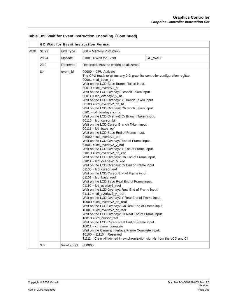
Graphics ControllerGraphics Controller Instruction Set
Copyright © 2009 Marvell Doc. No. MV-S301374-03 Rev. 2.0Version -
April 6, 2009 Released Page 285
12345678910111213141516171819202122232425262728293031323334353637383940414243444546474849505152535455565758
WD0 31:29 GCI Type 000 = Memory instruction
28:24 Opcode 01001 = Wait for Event GC_WAIT
23:9 Reserved Reserved. Must be written as all zeros.
8:4 event_id 00000 = CPU Activate The CPU reads or writes any 2-D graphics controller configuration register.00001 = cd_base_btWait on the LCD Base Branch Taken input.00010 = lcd_overlay1_bt Wait on the LCD Overlay1 Branch Taken input.00011 = lcd_overlay2_y_btWait on the LCD Overlay2 Y Branch Taken input.00100 = lcd_overlay2_cb_btWait on the LCD Overlay2 Cb ranch Taken input.0101 = cd_overlay2_cr_btWait on the LCD Overlay2 Cr Branch Taken input.00110 = lcd_cursor_btWait on the LCD Cursor Branch Taken input.00111 = lcd_base_eof Wait on the LCD Base End of Frame input.01000 = lcd_overlay1_eofWait on the LCD Overlay1 End of Frame input.01001 = lcd_overlay2_y_eofWait on the LCD Overlay2 Y End of Frame input.01010 = lcd_overlay2_cb_eofWait on the LCD Overlay2 Cb End of Frame input.01011 = lcd_overlay2_cr_eofWait on the LCD Overlay2 Cr End of Frame input01100 = lcd_cursor_eof Wait on the LCD Cursor End of Frame input.01101 = lcd_base_reofWait on the LCD Base Real End of Frame input.01110 = lcd_overlay1_reofWait on the LCD Overlay1 Real End of Frame input.01111 = lcd_overlay2_y_reof Wait on the LCD Overlay2 Y Real End of Frame input.10000 = lcd_overlay2_cb_reof Wait on the LCD Overlay2 Cb Real End of Frame input.10001 = lcd_overlay2_cr_reofWait on the LCD Overlay2 Cr Real End of Frame input.10010 = lcd_cursor_reofWait on the LCD Cursor Real End of Frame input.10011 = ci_frame_completeWait on the Camera Interface Frame Complete input.10100 – 11110 = Reserved11111 = Clear all latched in synchronization signals from the LCD and CI.
3:0 Word count 0b0000
Table 185: Wait for Event Instruction Encoding (Continued)
GC Wait for Event Instruct ion Format

PXA3xx (88AP3xx) Processor FamilyVolume III: Graphics and Input Controller Configuration Developers Manual
Doc. No. MV-S301374-03 Rev. 2.0 Version -
Copyright © 2009 Marvell
Page 286 April 6, 2009 Released
12345678910111213141516171819202122232425262728293031323334353637383940414243444546474849505152535455565758
4.6.2 2-D Graphics InstructionsSoftware must ensure that 2-D graphics operations do not run out of valid memory space. The graphics controller does not clip any output. Some examples of this are shown in Figure 72, “Illegal Addressing for 2-D Graphics Instructions. Any instructions performed like these have indeterminate results and memory contents cannot be guaranteed. No interrupt is generated for these cases.
Figure 72: Illegal Addressing for 2-D Graphics Instructions
4.6.2.1 Format for 2-D Instructions
Overview Short description of the instruction.
Usage How instruction is used (assembler mnemonic).
Qualifiers Descriptions of the qualifiers in the instruction usage.
Operation Pseudocode, equation, or flow map for instruction.
Exceptions Unsupported operations, formats, and so on.
Encoding Bitmap of instruction (memory image) as follows:
DX0DY0 (DX0,DY0)
DX0DY0
Table 186: General Instruction Encoding for 2-D Instructions
GC 2-D Instruct ion General Format
Bit 31 30 29 28 27 26 25 24 23 22 21 20 19 18 17 16 15 14 13 12 11 10 9 8 7 6 5 4 3 2 1 0
GCI Type
Opcode Raster Op Reserved Word Count
WD0 010 xxxxx xxxxxxxx 0 xxxx
WD1

Graphics ControllerGraphics Controller Instruction Set
Copyright © 2009 Marvell Doc. No. MV-S301374-03 Rev. 2.0Version -
April 6, 2009 Released Page 287
12345678910111213141516171819202122232425262728293031323334353637383940414243444546474849505152535455565758
WD0 Bits Name Descript ion
WD0 31:29 GCI Type 010 = 2-D graphics
28:24 Opcode 00000 = Color fill GC_CFILL
00001 = Chroma key BLT GC_CKBLT
00010 = Line draw GC_LINE
00011 = Anti-aliased line draw GC_AALINE
00100 = Reserved Reserved. Use of this opcode does not result in an Illegal Operation interrupt and may have indeterminate results.
00101 = Stretch BLT GC_STRBLT
00111 = Alpha Blend BLT GC_ABLND
01000 = Scale BLT GC_SCALE
01001 = Bias BLT GC_BIAS
01011 = Raster OP BLT GC_RAST
01100 = Pattern Copy BLT GC_PATT
01101 = Decimate BLT GC_DECBLT
01110 – 11111 = Reserved Reserved
23:16 Raster Op Selects one of 256 Raster Operations (See Section 4.6.2.11). Raster Operations are performed using Source 0, Source 1, and Destination as inputs. In the Raster Operation equations, S0 is Source 0, S1 is Source 1, and D is Destination.
15:4 Reserved Reserved. Must be written as all zeros.
3:0 Word count Word count for instruction. Starts at 0b0000 for 1 Word (WD0).
Table 186: General Instruction Encoding for 2-D Instructions (Continued)
GC 2-D Instruct ion General Format

PXA3xx (88AP3xx) Processor FamilyVolume III: Graphics and Input Controller Configuration Developers Manual
Doc. No. MV-S301374-03 Rev. 2.0 Version -
Copyright © 2009 Marvell
Page 288 April 6, 2009 Released
12345678910111213141516171819202122232425262728293031323334353637383940414243444546474849505152535455565758
4.6.2.2 Color Fill
Overview Fills the destination rectangle with the specified color (see Figure 73).
Figure 73: Color Fill Operation
Usage GC_CFILL< imm>DX0, DY0, width, height, reg, color
Qualifiers
Exceptions No raster operations are supported for the color fill instruction.
Clipping is not supported.
Encoding
Source 0 Source 1 Destination (Before)
Destination (After)
* An “X” through a buffer means this buffer is not usedfor this instruction.
X X X
Specified Color = DX0
DY0
Qualif ier Descript ion
imm 0 = Register contains color value1 = Immediate color value
Table 187: Color Fill Instruction Encoding
GC Color F i l l
B it 31 30 29 28 27 26 25 24 23 22 21 20 19 18 17 16 15 14 13 12 11 10 9 8 7 6 5 4 3 2 1 0
GCI Type
Opcode Register Reserved Pixel Format
Reserved
imm Word
Count
WD0 010 00000 0xxx 0 xxxx 0 x xxxx
WD1 Reserved DX0
WD2 Reserved DY0
WD3 Reserved Height Reserved Width
WD4 Color (if imm = ‘1’)
WD5 Color (if imm = ‘1’, optional, depends on Pixel Format)

Graphics ControllerGraphics Controller Instruction Set
Copyright © 2009 Marvell Doc. No. MV-S301374-03 Rev. 2.0Version -
April 6, 2009 Released Page 289
12345678910111213141516171819202122232425262728293031323334353637383940414243444546474849505152535455565758
WD0 Bits Name Descript ion
WD0 31:29 GCI Type “010” 2-D graphics
28:24 Opcode “00000” Color Fill GC_CFILL
23:20 Register If immediate is cleared, selects the graphics controller scratch register in which the color to be used is stored, and the WORD count is 0b0011. Valid registers are 0b0000 – 0b0111. Register values 0b1000 – 0b1111 are reserved for future expansion.If immediate is set, this field is NA and the WORD count is 0b0100 or 0b0101.
19:12 Reserved Reserved. Must be written as all zeros.
11:8 Pixel Format Immediate Color Pixel format. Does not apply if color is stored in register. The 4-bit pixel format for the buffer being programmed is placed here. This value is written to the corresponding configuration register. Refer to Table 131 for 4-bit format ID value.
7:5 Reserved Reserved. Must be written as all zeros.
4 Immediate 0 = Color Data is located in the register specified in WD0:Register.1 = Color Data is supplied in the instruction stream
3:0 Word Count Depends on Pixel Format and imm. Can be 0b0011, 0b0100 or 0b0101.
WD1 Bits Name Descript ion
WD1 31:11 Reserved Reserved. Must be written as all zeros.
10:0 DX0 Starting pixel number of destination block
WD2 Bits Name Descript ion
WD2 31:11 Reserved Reserved. Must be written as all zeros.
10:0 DY0 Starting line number of destination block
WD3 Bits Name Descript ion
WD3 31:27 Reserved Reserved. Must be written as all zeros.
26:16 Height Positive Unsigned Integer Pixel Height of the Block
15:11 Reserved Reserved. Must be written as all zeros.
10:0 Width Positive Unsigned Integer Pixel Width of the Block
WD4 Dependency Bits Name Descript ion
WD4 WD0:imm = ‘0’ NA NA This word is not valid for this dependency condition.
WD0:imm = ‘1’ 31:0 Color Contains the first word of the color data
Table 187: Color Fill Instruction Encoding (Continued)
GC Color F i l l

PXA3xx (88AP3xx) Processor FamilyVolume III: Graphics and Input Controller Configuration Developers Manual
Doc. No. MV-S301374-03 Rev. 2.0 Version -
Copyright © 2009 Marvell
Page 290 April 6, 2009 Released
12345678910111213141516171819202122232425262728293031323334353637383940414243444546474849505152535455565758
4.6.2.3 Chroma Key BLT
Overview Replaces the destination pixel with the source 0 pixel if the destination color is greater than a specified threshold. The operation can also be inverted through the <invert> qualifier. The source 0 and destination must be the same size in pixel width and height, but they can have different pixel formats. For indexed color format the range refers to the index range.
Figure 74: Chroma Key BLT Operation
Usage GC_CKBLT<invert>, DX0, DY0, SX0, SY0, width, height, threshold, key
The algorithm to determine whether the pixel value falls within the chroma key range is described here. If the key color is blue (this is programmable; alpha is not a valid key color), the distance used to calculate the difference between the destination and chroma key can be measured as follows:
dest_dist = 2*destination(blue) - destination(red) - destination(green)
WD5 Dependency Bits Name Descript ion
WD5 WD0:imm = ‘0’ NA NA This word is not valid for this dependency condition.
WD0:imm = ‘1’ 31:0 Color Contains the second word of the color data if the pixel format calls for a second WORD. See Table 131 for Pixel Format Decoding. If pixel format does not require a second word count, the word count is 0b0100, not 0b0101.
Table 187: Color Fill Instruction Encoding (Continued)
GC Color F i l l
Source 0 Source 1 Destination (before)
Destination (after - no inversion)
* An “X” through a buffer means this buffer is not usedfor this instruction.
X
Threshold Value =
Destination (after - with inversion)
DX0DY0
DX0DY0
DX0DY0
SX0SY0

Graphics ControllerGraphics Controller Instruction Set
Copyright © 2009 Marvell Doc. No. MV-S301374-03 Rev. 2.0Version -
April 6, 2009 Released Page 291
12345678910111213141516171819202122232425262728293031323334353637383940414243444546474849505152535455565758
Thus, the chroma key evaluates true if:
(dest_dist > threshold)
The behavior of the instruction can be defined as follows:
if (invert == 0) if (dest_dist < saturation) && (dest_dist > threshold) then
destination = source0;else
destination = destination;end if
else if (dest_dist < saturation) && (dest_dist > threshold) then
destination = destination;else
destination = source0;end if
end if
Qualifiers
Exceptions No Raster Operations are supported for chroma Key BLT.
The Source 0 region and Destination region cannot overlap.
Clipping is not supported.
Encoding
Qualif ier Descript ion
invert Inverts the logical replacement decision operation.
Table 188: Chroma Key BLT Instruction Encoding
GC Chroma Key BLT
Bit 31 30 29 28 27 26 25 24 23 22 21 20 19 18 17 16 15 14 13 12 11 10 9 8 7 6 5 4 3 2 1 0
GCI Type
Opcode Reserved
Inv
ert Word
Count
WD0 010 00001 0 x 0110
WD1 Reserved DX0
WD2 Reserved DY0
WD3 Reserved SX0
WD4 Reserved SY0
WD5 Reserved Height Reserved Width
WD6 Reserved Key Threshold Value

PXA3xx (88AP3xx) Processor FamilyVolume III: Graphics and Input Controller Configuration Developers Manual
Doc. No. MV-S301374-03 Rev. 2.0 Version -
Copyright © 2009 Marvell
Page 292 April 6, 2009 Released
12345678910111213141516171819202122232425262728293031323334353637383940414243444546474849505152535455565758
WD0 Bits Name Descript ion
WD0 31:29 GCI Type 010 = 2-D graphics
28:24 Opcode 00001 = Chroma Key BLT GC_CKBLT
23:5 Reserved Reserved. Must be written as all zeros.
4 invert 0 = Do not invert logical chroma key operation.1 = Invert logical chroma key operation
3:0 Word Count 0b0110
WD1 Bits Name Descript ion
WD1 31:11 Reserved Reserved. Must be written as all zeros.
10:0 DX0 Starting pixel number of destination block
WD2 Bits Name Descript ion
WD2 31:11 Reserved Reserved. Must be written as all zeros.
10:0 DY0 Starting line number of destination block
WD3 Bits Name Descript ion
WD3 31:11 Reserved Reserved. Must be written as all zeros.
10:0 SX0 Starting pixel number of source 0 block
WD4 Bits Name Descript ion
WD4 31:11 Reserved Reserved. Must be written as all zeros.
10:0 SY0 Starting line number of source 0 block
WD5 Bits Name Descript ion
WD5 31:27 Reserved Reserved. Must be written as all zeros.
26:16 Height Positive Unsigned Integer Pixel Height of the Block
15:11 Reserved Reserved. Must be written as all zeros.
10:0 Width Positive Unsigned Integer Pixel Width of the Block
Table 188: Chroma Key BLT Instruction Encoding (Continued)
GC Chroma Key BLT

Graphics ControllerGraphics Controller Instruction Set
Copyright © 2009 Marvell Doc. No. MV-S301374-03 Rev. 2.0Version -
April 6, 2009 Released Page 293
12345678910111213141516171819202122232425262728293031323334353637383940414243444546474849505152535455565758
4.6.2.4 Line Draw
Overview Draws a line of specified width into the destination starting at origin with color specified in instruction stream or register.
• DX0 is the X-coordinate of the starting pixel in the line
• DY0 is the Y-coordinate of the starting pixel in the line
• DX1 is the X-coordinate of the ending pixel in the line
• DY1 is the Y-coordinate of the ending pixel in the line
Figure 75: Line Draw Operation
Usage GC_LINE< imm> DX0, DY0, X_is_1, Y_is_1, X_dir, Y_dir, DeltaX, DeltaY, Length, Width, Rn or Color
Qualifiers
WD6 Bits Name Descript ion
WD6 28:19 Reserved Reserved. Must be written as all zeros.
18:17 Key Color 00 = Use Blue as the key color01 = Use Green as the key color10 = Use Red as the key color11 = Alpha is not a valid key; Use Blue as the key color
16:0 Threshold Contains the 17-bit threshold value used for comparisons.
Table 188: Chroma Key BLT Instruction Encoding (Continued)
GC Chroma Key BLT
Quali f ier Descript ion
imm Asserted for immediate color value.De-asserted if the register contains the color value.
Source 0 Source 1 Destination (before)
Destination (after)
* An “X” through a buffer means this buffer is not usedfor this instruction.
X X X
Specified Color = (DX0,DY0)
length=4(pixels)DeltaX
DeltaY

PXA3xx (88AP3xx) Processor FamilyVolume III: Graphics and Input Controller Configuration Developers Manual
Doc. No. MV-S301374-03 Rev. 2.0 Version -
Copyright © 2009 Marvell
Page 294 April 6, 2009 Released
12345678910111213141516171819202122232425262728293031323334353637383940414243444546474849505152535455565758
Operation The Line Draw instruction is a simple memory fill engine. The DeltaX and DeltaY parameters are subpixel precision factors that define the slope of the line. The values DeltaX and DeltaY are calculated as follows:
The direction of the line is determined by the X_dir and the Y_dir directions. Both DeltaX and DeltaY are 14-bit unsigned fractional numbers. The precision of these factors (and therefore of the address generator) must be such that the accumulated error over a full screen is less than one pixel. Therefore, for a 1024 × 768 display, the error should be less than 1/1024. The subpixel precision must be 10 bits. Fourteen bits are used for future expansion, and all 14 bits are considered in calculations. However, only the upper 10 bits should be programmed as non-zero. The lower 4 bits must be programmed to zero. The length of the line is the number of pixels in the major direction of the line. The width of the line is the number of pixels in the non-major direction to draw for each step taken in the major direction.
X_is_1/Y_is_1 determines that the line moves one pixel in the X/Y direction (major direction) every step. The DeltaX/DeltaY fractions determines how much of a fractional pixel the line moves in the X/Y direction (minor direction) every step. For reference, either X_is_1 or Y_is_1 must be 0b1. When one of these is set to 1, the corresponding Delta must be all zeros. If it is configured to anything else, it is overridden and cleared to all zeros.
X_dir and Y_dir control the direction in which the line is written to the buffer. When X_dir is 1, the line is written left to right; when X_dir is 0, the line is written right to left. When Y_dir is 1, the line is written bottom to top, when Y_dir is 0, the line is written from top to bottom.
Figure 76 shows the use of the programmable fields X_dir, Y_dir, X_is_1, Y_is_1, DeltaX, and DeltaY.
DeltaY 1 slope–= For 315° < angles <45° and 135° < angles
DeltaX 1 1slope---------------–= For 45° < angles <135° and 225° < angles <315°

Graphics ControllerGraphics Controller Instruction Set
Copyright © 2009 Marvell Doc. No. MV-S301374-03 Rev. 2.0Version -
April 6, 2009 Released Page 295
12345678910111213141516171819202122232425262728293031323334353637383940414243444546474849505152535455565758
Figure 76: Use of Programmable Values for Line Draw
Corner cases are shown in Figure 76. These are general rules to be followed for the line draw. The basic line draw algorithm is described by the set of rules given in Figure 77.
X_dir = ‘1’Y_dir = ‘1’X_is_1 = ‘1’Y_is_1 = ‘0’DeltaX = 0hDeltaY = value
X_dir = ‘1’Y_dir = ‘1’ or ‘0’X_is_1 = ‘1’Y_is_1 = ‘0’DeltaX = 0hDeltaY = 0h
> 0 degrees< 45 degrees
0 degrees
X_dir = ‘1’Y_dir = ‘0’X_is_1 = ‘1’Y_is_1 = ‘0’DeltaX = 0hDeltaY = value
> 315 degrees< 360 degrees
X_dir = ‘0’Y_dir = ‘1’ or ‘0’X_is_1 = ‘1’Y_is_1 = ‘0’DeltaX = 0hDeltaY = 0h
180 degrees
X_dir = ‘1’Y_dir = ‘1’X_is_1 = ‘1’Y_is_1 = ‘1’DeltaX = 0hDeltaY = 0h
45 degrees
X_dir = ‘1’Y_dir = ‘0’X_is_1 = ‘1’Y_is_1 = ‘1’DeltaX = 0hDeltaY = 0h
315 degrees
X_dir = ‘0’Y_dir = ‘0’X_is_1 = ‘1’Y_is_1 = ‘0’DeltaX = 0hDeltaY = value
> 180 degrees< 225 degrees
Y_dir = ‘0’X_is_1 = ‘1’Y_is_1 = ‘1’DeltaX = 0hDeltaY = 0h
225 degrees X_dir = ‘0’
X_dir = ‘0’Y_dir = ‘1’X_is_1 = ‘1’Y_is_1 = ‘0’DeltaX = 0hDeltaY = value
> 135 degrees< 180 degrees
135 degrees X_dir = ‘0’Y_dir = ‘1’X_is_1 = ‘1’Y_is_1 = ‘1’DeltaX = 0hDeltaY = 0h
X_dir = ‘1’Y_dir = ‘1’X_is_1 = ‘0’Y_is_1 = ‘1’DeltaX = valueDeltaY = 0h
> 45 degrees< 90 degrees
> 90 degrees< 135 degrees
X_dir = ‘0’Y_dir = ‘1’X_is_1 = ‘0’Y_is_1 = ‘1’DeltaX = valueDeltaY = 0h
X_dir = ‘1’ or ‘0’Y_dir = ‘1’X_is_1 = ‘0’Y_is_1 = ‘1’DeltaX = 0hDeltaY = 0h
90 degrees
X_dir = ‘1’ or ‘0’Y_dir = ‘0’X_is_1 = ‘0’Y_is_1 = ‘1’DeltaX = 0hDeltaY = 0h
270 degrees
X_dir = ‘1’Y_dir = ‘0’X_is_1 = ‘0’Y_is_1 = ‘1’DeltaX = valueDeltaY = 0h
X_dir = ‘0’Y_dir = ‘0’X_is_1 = ‘0’Y_is_1 = ‘1’DeltaX = valueDeltaY = 0h
> 270 degrees< 315 degrees
> 225 degrees< 270 degrees

PXA3xx (88AP3xx) Processor FamilyVolume III: Graphics and Input Controller Configuration Developers Manual
Doc. No. MV-S301374-03 Rev. 2.0 Version -
Copyright © 2009 Marvell
Page 296 April 6, 2009 Released
12345678910111213141516171819202122232425262728293031323334353637383940414243444546474849505152535455565758
Figure 77: Line Draw Algorithm Rules
Example 4. Line Draw Algorithm
For all the examples shown here, DX0 = 10, DY0 = 10 (this position is indicated by an “S” in this position), Length = 8, and Width = 1. The major direction is the direction with X_is_1/Y_is_1 set to 1. The minor direction is the direction with X_is_1/Y_is_1 cleared to 0. If both are set to 1, then the line is at a 45 degree angle. These examples show that the major direction is incremented or decremented by 1 and the non-major direction is incremented or decremented by the delta value. The non-major coordinate for each pixel is calculated by truncating the non-major value. The numbers to the side of the line indicate the values of the non-major direction for each pixel.
X_dir = ‘1’, X_is_1 = ‘1’, DeltaX = 0x0
Y_dir = ‘1’, Y_is_1 = ‘0’, DeltaY = 0x1000 (1/4)
> 0 degrees< 45 degrees
0 degrees
> 315 degrees< 360 degrees
180 degrees
45 degrees
315 degrees
> 180 degrees< 225 degrees
225 degrees
> 135 degrees< 180 degrees
135 degrees
Add DeltaX> 45 degrees< 90 degrees
> 90 degrees< 135 degrees
90 degrees
270 degrees
> 270 degrees< 315 degrees
> 225 degrees< 270 degrees
to DX value
SubtractDeltaY fromDY value
Add DeltaYto DY value
Add DeltaXto DX value
SubtractDeltaX fromDX value
Add DeltaYto DY value
SubtractDeltaY fromDY value
SubtractDeltaX fromDX value
8 X X X 8.75, 8.5, 8.25
9 X X X X 9.75, 9.5, 9.25, 9
10 S 10
10
11
12
13
14
15
16
17

Graphics ControllerGraphics Controller Instruction Set
Copyright © 2009 Marvell Doc. No. MV-S301374-03 Rev. 2.0Version -
April 6, 2009 Released Page 297
12345678910111213141516171819202122232425262728293031323334353637383940414243444546474849505152535455565758
X_dir = ‘1’, X_is_1 = ‘0’, DeltaX = 0x1000 (1/4)
Y_dir = ‘1’, Y_is_1 = ‘1’, DeltaY = 0x0
X_dir = ‘0’, X_is_1 = ‘0’, DeltaX = 0x1000 (1/4)
Y_dir = ‘1’, Y_is_1 = ‘1’, DeltaY = 0x0
3 X
4 X
5 X
6 X
7 X
8 X
9 X
10 S
10 11
10,10.25,10.5,10.75
11,11.25,11.5,11.75
X 3
X 4
X 5
X 6
X 7
X 8
X 9
S 10
8 9 10
8.75,8.5,8.25
9.75,9.5,9.25,9
10

PXA3xx (88AP3xx) Processor FamilyVolume III: Graphics and Input Controller Configuration Developers Manual
Doc. No. MV-S301374-03 Rev. 2.0 Version -
Copyright © 2009 Marvell
Page 298 April 6, 2009 Released
12345678910111213141516171819202122232425262728293031323334353637383940414243444546474849505152535455565758
X_dir = ‘0’, X_is_1 = ‘1’, DeltaX = 0x0
Y_dir = ‘1’, Y_is_1 = ‘0’, DeltaY = 0x1000 (1/4)
X_dir = ‘0’, X_is_1 = ‘1’, DeltaX = 0x0
Y_dir = ‘0’, Y_is_1 = ‘0’, DeltaY = 0x1000 (1/4)
X_dir = ‘0’, X_is_1 = ‘0’, DeltaX = 0x1000 (1/4)
Y_dir = ‘0’, Y_is_1 = ‘1’, DeltaY = 0x0
8.75, 8.5, 8.25 X X X 8
9.75, 9.5, 9.25, 9
X X X X 9
10 S 10
3 4 5 6 7 8 9 10
3 4 5 6 7 8 9 10
10, 10.25, 10.5, 10.75
X X X S 10
11, 11.25, 11.5, 11.75
X X X X 11
8 9 10
S 10
X 11
X 12
X 13
X 14
X 15
X 16

Graphics ControllerGraphics Controller Instruction Set
Copyright © 2009 Marvell Doc. No. MV-S301374-03 Rev. 2.0Version -
April 6, 2009 Released Page 299
12345678910111213141516171819202122232425262728293031323334353637383940414243444546474849505152535455565758
X_dir = ‘1’, X_is_1 = ‘0’, DeltaX = 0x1000 (1/4)
Y_dir = ‘0’, Y_is_1 = ‘1’, DeltaY = 0x0
X_dir = ‘1’, X_is_1 = ‘1’, DeltaX = 0x0
Y_dir = ‘0’, Y_is_1 = ‘0’, DeltaY = 0x1000 (1/4)
The graphics controller does not exactly follow the algorithm for the case when Y_is_1 = 0b1 and X_is_1 = 0b0. Software must adjust the GC_LINE instruction to get the desired result. The software must make the follow adjustment to the DX0 pixel coordinate to achieve the results as described in the line draw algorithm.
X 17
8.75,8.5,8.25
9.75,9.5,9.25,9
10
10 11
10 S
11 X
12 X
13 X
14 X
15 X
16 X
17 X
10,10.25,10.5,10.75
11,11.25,11.5,11.75
10
11
12
13
14
15
16
17
10
S X X X 10, 10.25, 10.5, 10.75
11
X X X X 11, 11.25, 11.5, 11.75

PXA3xx (88AP3xx) Processor FamilyVolume III: Graphics and Input Controller Configuration Developers Manual
Doc. No. MV-S301374-03 Rev. 2.0 Version -
Copyright © 2009 Marvell
Page 300 April 6, 2009 Released
12345678910111213141516171819202122232425262728293031323334353637383940414243444546474849505152535455565758
• DX0 = (DX0 - 1).(1 - DeltaX) [region > 45 degrees and < 90 degrees]
• DX0 = (DX0 - 1).(1 - DeltaX) [region > 270 degrees and < 315 degrees]
• DX0 = DX0.DeltaX [region > 90 degrees and < 135 degrees]
• DX0 = DX0.DeltaX [region > 225 degrees and < 270 degrees
The graphics controller does not correctly draw the line in the following cases:
• If a line of length greater than 1 with X_is_1 = 1 must display the ending pixel at DX1 = 0, then the ending pixel is not displayed.
• If a line of length = 1 must display the ending pixel at DX1 = 0, the pixel is either displayed in an invalid location or is not displayed at all.
Software must use the boundary check equations that account for the width of the line and the fact that a GC_AALINE adds 4 pixels on each side of the line in the non-major direction of the line. Software must check the line boundaries and if the line is going to be drawn incorrectly, software must reverse the line direction so that the starting pixel is at DX0 = 0 instead of the ending pixel at DX1 = 0.
Figure 78: Examples of Line Draw DelX, DelY, and Length
Line 0 Line 1
Line 2
Line 3
Line 4
Line 5
Line 6Line 7
Line 8Line 9Line 10
Line 11
Line 12
Line 13 Line 14
Line 15
Table 189: Example Programmable Value for Line Draw (See Figure 78)
Line Actual DeltaXValue
Programmed Value Actual DeltaYValue
Programmed Value Length
X_
dir
X_
is_
1
DeltaX(13:0)
Y_
dir
Y_
is_
1
De
lta
Y(1
3:0
) Actual Value
Programmed Value (10:0)
Line 0 0 1 0 0x0000 +1 1 1 0x0000 2 00000000010

Graphics ControllerGraphics Controller Instruction Set
Copyright © 2009 Marvell Doc. No. MV-S301374-03 Rev. 2.0Version -
April 6, 2009 Released Page 301
12345678910111213141516171819202122232425262728293031323334353637383940414243444546474849505152535455565758
Example 5. Line Draw
To illustrate the software workaround for the line with Y_is_1 = 1, Line 7 from Table 189 is used. .
Line 1 +1/2 1 0 0x2000 +1 1 1 0x0000 2 00000000010
Line 2 +1 1 1 0x0000 +1 1 1 0x0000 6 00000000110
Line 3 +1 1 1 0x0000 +5/9 1 0 0x2390 9 00000001001
Line 4 +1 1 1 0x0000 0 1 0 0x0000 8 00000001000
Line 5 +1 1 1 0x0000 –1/7 0 0 0x0920 7 00000000111
Line 6 +1 1 1 0x0000 –1 0 1 0x0000 4 00000000100
Line 7 +1/2 1 0 0x2000 –1 0 1 0x0000 4 00000000100
Line 8 0 1 0 0x0000 –1 0 1 0x0000 5 00000000101
Line 9 –1/5 0 1 0x0cd0 –1 0 1 0x0000 5 00000000101
Line 10 –1 0 1 0x0000 –1 0 1 0x0000 5 00000000101
Line 11 –1 0 1 0x0000 –2/3 0 0 0x2ab0 3 00000000011
Line 12 –1 0 1 0x0000 0 1 0 0x0000 10 00000001010
Line 13 –1 0 1 0x0000 +3/5 1 0 0x2660 5 00000000101
Line 14 –1 0 1 0x0000 +1 1 1 0x0000 3 00000000011
Line 15 –2/5 0 1 0x19a0 +1 1 1 0x0000 5 00000000101
Table 189: Example Programmable Value for Line Draw (See Figure 78) (Continued)
Line Actual DeltaXValue
Programmed Value Actual DeltaYValue
Programmed Value Length
X_
dir
X_
is_
1
DeltaX(13:0)
Y_
dir
Y_
is_
1
De
lta
Y(1
3:0
) Actual Value
Programmed Value (10:0)
Line 7
X_dir = ‘1’
Y_dir = ‘1’
X_is_1 = ‘0’
Y_is_1 = ‘1’
DelX = 2000h (1/2)
DelY = 0h
> 45 degrees
< 90 degrees
(0,0)
(4,5)
Length = 5
Width = 5
DX0 = 4
DY0 = 5

PXA3xx (88AP3xx) Processor FamilyVolume III: Graphics and Input Controller Configuration Developers Manual
Doc. No. MV-S301374-03 Rev. 2.0 Version -
Copyright © 2009 Marvell
Page 302 April 6, 2009 Released
12345678910111213141516171819202122232425262728293031323334353637383940414243444546474849505152535455565758
Figure 79: Detailed drawing of Resulting Line (With Boerne Line DX0 = 4.0)
The figure below shows the line that the graphics controller draws with the software workaround. The software sets DX0 = (DX0 - 1).(1 - DeltaX) = 3.5 to get the correct result.
Figure 80: Detailed drawing of Resulting Line (With Boerne Line DX0 = 3.5)
Exceptions Line Draw does not support raster operations.
Lines are not clipped, so a line that extends beyond the edge of the display may alias into another part of the display or into illegal memory areas. Table 190 shows how to calculate the boundaries of the line. The boundaries are defined by the coordinates (DX0, DY0) and (DX1, DY1). If the boundaries of the line extend beyond the edge of the display, the software must clip the line by adjusting the starting coordinates and/or length.
(4,5)
Single width
(4.5,4)
(5,3)
(5.5,2)
(6,1)
Single widthperfect line Boerne Line
(4,5)
(5,4)
(5,3)
(6,2)
(6,1)
Width = 5Boerne Line
Width = 5Perfect Line
(6,5)(2,5)
(2.5,4)
(3,3)
(3.5,2)
(4,1)
(6.5,4)
(7,3)
(7.5,2)
(8,1)
(2,5)
(3,4)
(3,3)
(4,2)
(4,1)
(6,5)
(7,4)
(7,3)
(8,2)
(8,1)
(4,5)
Single width
(4.5,4)
(5,3)
(5.5,2)
(6,1)
Single widthperfect line Boerne Line
(4,5)
(4,4)
(5,3)
(5,2)
(6,1)
Width = 5Boerne Line
Width = 5Perfect Line
(6,5)(2,5)
(2.5,4)
(3,3)
(3.5,2)
(4,1)
(6.5,4)
(7,3)
(7.5,2)
(8,1)
(2,5)
(2,4)
(3,3)
(3,2)
(4,1)
(6,5)
(6,4)
(7,3)
(7,2)
(8,1)
Table 190: Line Boundaries for GC_LINE
Region Major Direction Boundaries Non-Major Direct ion Boundaries
0 to 45 degrees DX0 = DX0 DY0 = DY0 + [(Width – 1)/2]
DX1 = DX0 + (Length – 1) DY1 = DY0 - CEIL[(Length – 1)*Delta] – [(Width – 1)/2]
45 to 90 degrees DY0 = DY0 DX0 = DX0 – [(Width - 1)/2]
DY1 = DY0 – (Length – 1) DX1 = DX0 + FLOOR[(Length – 1)*Delta] + [(Width – 1)/2]
90 to 135 degrees DY0 = DY0 DX0 = DX0 + [(Width – 1)/2]
DY1 = DY0 – (Length - 1) DX1 = DX0 - CEIL[(Length – 1)*Delta] – [(Width – 1)/2]
135 to 180 degrees DX0 = DX0 DY0 = DY0 + [(Width – 1)/2]
DX1 = DX0 – (Length – 1) DY1 = DY0 – CEIL[(Length – 1)*Delta] – [(Width – 1)/2]
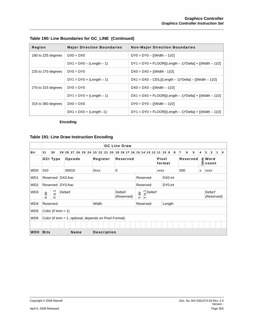
Graphics ControllerGraphics Controller Instruction Set
Copyright © 2009 Marvell Doc. No. MV-S301374-03 Rev. 2.0Version -
April 6, 2009 Released Page 303
12345678910111213141516171819202122232425262728293031323334353637383940414243444546474849505152535455565758
Encoding
180 to 225 degrees DX0 = DX0 DY0 = DY0 – [(Width – 1)/2]
DX1 = DX0 – (Length – 1) DY1 = DY0 + FLOOR[(Length – 1)*Delta] + [(Width – 1)/2]
225 to 270 degrees DY0 = DY0 DX0 = DX0 + [(Width - 1)/2]
DY1 = DY0 + (Length – 1) DX1 = DX0 – CEIL[(Length – 1)*Delta] – [(Width – 1)/2]
270 to 315 degrees DY0 = DY0 DX0 = DX0 – [(Width – 1)/2]
DY1 = DY0 + (Length – 1) DX1 = DX0 + FLOOR[(Length – 1)*Delta] + [(Width – 1)/2]
315 to 360 degrees DX0 = DX0 DY0 = DY0 – [(Width – 1)/2]
DX1 = DX0 + (Length –1) DY1 = DY0 + FLOOR[(Length – 1)*Delta] + [(Width – 1)/2]
Table 190: Line Boundaries for GC_LINE (Continued)
Region Major Direction Boundaries Non-Major Direct ion Boundaries
Table 191: Line Draw Instruction Encoding
GC Line Draw
Bit 31 30 29 28 27 26 25 24 23 22 21 20 19 18 17 16 15 14 13 12 11 10 9 8 7 6 5 4 3 2 1 0
GCI Type Opcode Register Reserved Pixel format
Reserved
imm Word
count
WD0 010 00010 0xxx 0 xxxx 000 x xxxx
WD1 Reserved DX0.frac Reserved DX0.int
WD2 Reserved DY0.frac Reserved DY0.int
WD3
X d
ir
X is
1 DeltaX DeltaX (Reserved) Y
dir
Y is
1 DeltaY DeltaY (Reserved)
WD4 Reserved Width Reserved Length
WD5 Color (if imm = 1)
WD6 Color (if imm = 1, optional, depends on Pixel Format)
WD0 Bits Name Descript ion

PXA3xx (88AP3xx) Processor FamilyVolume III: Graphics and Input Controller Configuration Developers Manual
Doc. No. MV-S301374-03 Rev. 2.0 Version -
Copyright © 2009 Marvell
Page 304 April 6, 2009 Released
12345678910111213141516171819202122232425262728293031323334353637383940414243444546474849505152535455565758
WD0 31:29 GCI Type 0b010 2-D graphics
28:24 Opcode “00010” Line Draw GC_LINE
23:20 Register If immediate = 0, selects graphics controller scratch register in which to store the color to be used, and the WORD count is 0b0100. Valid registers are 0b0000–0b0111. Register values 0b1000– 0b1111 are reserved for future expansion.If immediate = 1, this field is NA and the WORD count is 0b0101 or 0b0110.
19:12 Reserved Reserved. Must be written as all zeros.
11:8 Pixel Format Immediate color pixel format. Does not apply if the color is stored in the register. The 4-bit pixel format for the buffer being programmed is placed here. This value is written to the corresponding configuration register. Refer to Table 131 on page 257 for 4-bit format ID value.
7:5 Reserved Reserved. Must be written as all zeros.
4 Immediate 0 = Color Data is located in the specified register in WD0:Register.1 = Color Data is supplied in the instruction stream
3:0 Word Count Depends on pixel format and immediate. Can be 0b0100, 0b0101, or 0b0110.
WD1 Bits Name Descript ion
WD1 31:30 Reserved Reserved. Must be written as all zeros.
29:16 DX0.frac Origin pixel number of destination block (fractional value)
15:11 Reserved Reserved. Must be written as all zeros.
10:0 DX0.int Origin pixel number of destination block (integer value)
WD2 Bits Name Descript ion
WD2 31:30 Reserved Reserved. Must be written as all zeros.
29:16 DY0.frac Origin line number of destination line (fractional value)
15:11 Reserved Reserved. Must be written as all zeros.
10:0 DY0.int Origin line number of destination line (integer value)
WD3 Bits Name Descript ion
31 X dir The direction for the X portion of the line. If X_dir is programmed to 1, the line drawn falls in the range of –90 degrees to 90 degrees.
Table 191: Line Draw Instruction Encoding (Continued)
GC Line Draw
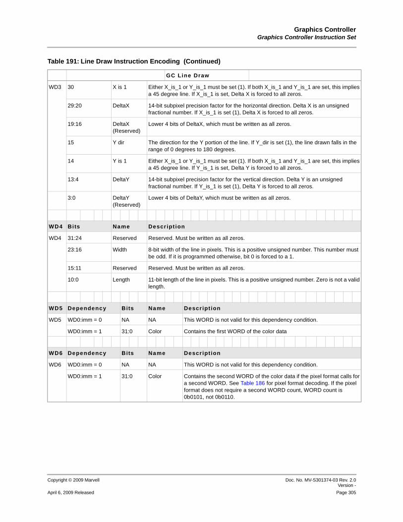
Graphics ControllerGraphics Controller Instruction Set
Copyright © 2009 Marvell Doc. No. MV-S301374-03 Rev. 2.0Version -
April 6, 2009 Released Page 305
12345678910111213141516171819202122232425262728293031323334353637383940414243444546474849505152535455565758
WD3 30 X is 1 Either X_is_1 or Y_is_1 must be set (1). If both X_is_1 and Y_is_1 are set, this implies a 45 degree line. If X_is_1 is set, Delta X is forced to all zeros.
29:20 DeltaX 14-bit subpixel precision factor for the horizontal direction. Delta X is an unsigned fractional number. If X_is_1 is set (1), Delta X is forced to all zeros.
19:16 DeltaX (Reserved)
Lower 4 bits of DeltaX, which must be written as all zeros.
15 Y dir The direction for the Y portion of the line. If Y_dir is set (1), the line drawn falls in the range of 0 degrees to 180 degrees.
14 Y is 1 Either X_is_1 or Y_is_1 must be set (1). If both X_is_1 and Y_is_1 are set, this implies a 45 degree line. If Y_is_1 is set, Delta Y is forced to all zeros.
13:4 DeltaY 14-bit subpixel precision factor for the vertical direction. Delta Y is an unsigned fractional number. If Y_is_1 is set (1), Delta Y is forced to all zeros.
3:0 DeltaY (Reserved)
Lower 4 bits of DeltaY, which must be written as all zeros.
WD4 Bits Name Descript ion
WD4 31:24 Reserved Reserved. Must be written as all zeros.
23:16 Width 8-bit width of the line in pixels. This is a positive unsigned number. This number must be odd. If it is programmed otherwise, bit 0 is forced to a 1.
15:11 Reserved Reserved. Must be written as all zeros.
10:0 Length 11-bit length of the line in pixels. This is a positive unsigned number. Zero is not a valid length.
WD5 Dependency Bits Name Descript ion
WD5 WD0:imm = 0 NA NA This WORD is not valid for this dependency condition.
WD0:imm = 1 31:0 Color Contains the first WORD of the color data
WD6 Dependency Bits Name Descript ion
WD6 WD0:imm = 0 NA NA This WORD is not valid for this dependency condition.
WD0:imm = 1 31:0 Color Contains the second WORD of the color data if the pixel format calls for a second WORD. See Table 186 for pixel format decoding. If the pixel format does not require a second WORD count, WORD count is 0b0101, not 0b0110.
Table 191: Line Draw Instruction Encoding (Continued)
GC Line Draw

PXA3xx (88AP3xx) Processor FamilyVolume III: Graphics and Input Controller Configuration Developers Manual
Doc. No. MV-S301374-03 Rev. 2.0 Version -
Copyright © 2009 Marvell
Page 306 April 6, 2009 Released
12345678910111213141516171819202122232425262728293031323334353637383940414243444546474849505152535455565758
4.6.2.5 Anti-Aliased Line Draw
Overview Draws an anti-aliased line of a specified width starting at the origin with the color specified in the instruction stream of register and the coefficient mask stored in memory.
Figure 81: Anti-Aliased Line Draw Operation
Usage GC_AALINE< imm> DX0, DY0, X_is_1, Y_is_1, X_dir, Y_dir, DelX, DelY, width, length, address, Rn or Color
Qualifiers
Operation The anti-aliased line draw instruction performs a very simple pre-rasterization to generate an anti-aliased line. This instruction is identical to the regular line draw for the regular part of the line. In addition, four pixels on each side of the line in the non-major direction are multiplied by a coefficient array. Only the red, green, and blue components are multiplied by the 8-bit unsigned coefficient. The alpha or transparency component is left unchanged. The CPU performs the pre-rasterization. The coefficients must be stored in a mask array in memory. The anti-aliasing is performed in the non-major direction of the line.
The mask array is eight 8-bit coefficients. Each 8-bit coefficient in the line represents the proper rasterized values for a 1/8 pixel subassembly. Therefore, for this instruction, 64-bits are read from memory for the coefficients. These coefficients are 8-bit unsigned fractional values, so 1.0 cannot be a coefficient because the closest approximation to 1.0 is 0xFF. These 8 coefficients stored in memory must be 8-byte aligned in memory.
Figure 82 shows the effect of anti-aliasing the line draw.
Quali f ier Descript ion
imm Asserted for register colorDe-asserted for Pointer to color in memory
Source 0 Source 1 Destination (Before)
Destination (After)
* An “X” through a buffer means this buffer is not usedfor this instruction.
X X X
Specified Color = Length=4(Steps)
(DX0,DY0)
DelX
DelY

Graphics ControllerGraphics Controller Instruction Set
Copyright © 2009 Marvell Doc. No. MV-S301374-03 Rev. 2.0Version -
April 6, 2009 Released Page 307
12345678910111213141516171819202122232425262728293031323334353637383940414243444546474849505152535455565758
Figure 82: Effects of Anti-Aliased Line Drawing
The general anti-aliasing algorithm involves 2-D conics for performing anti-aliasing operations. The conics (referred to as the mask) are loaded from memory. The mask/conics is applied horizontally or vertically based on the slope of the line. Because the lines here are linear, notches and so on are easily avoided. An example of a row in the mask/conics is shown in Figure 83.
Figure 83: Example of Anti-Aliased commands
The anti-aliased line draw algorithm is identical to the line draw algorithm with the addition that it displays 4 pixels on each side of the line in the non-major direction.
Warning
Warning The software must use the same work-arounds that it does for the GC_LINE instruction.
Figure 84 shows the line that the graphics controller draws without the software workaround.
CC996633 4477AADD100
Actual Line Cross Section:
b1 b2 b3 b4 b5 b6 b7 b8 b9
System Bus 2 Coefficient Ordering:
63 Down To 0
33 66 99 CC DD AA 77 44
(For an explanation of bx, see the discussion of theLine Draw Algorithm.)
Coefficients above are read from System Bus 2and ordered as follows.

PXA3xx (88AP3xx) Processor FamilyVolume III: Graphics and Input Controller Configuration Developers Manual
Doc. No. MV-S301374-03 Rev. 2.0 Version -
Copyright © 2009 Marvell
Page 308 April 6, 2009 Released
12345678910111213141516171819202122232425262728293031323334353637383940414243444546474849505152535455565758
Figure 84: Drawing of Resulting Anti-Aliased Line from Example 5 (DX0 = 4.0)
Figure 85 shows the line that the graphics controller draws with the software workaround. The software sets DX0 = (DX0 – 1).(1– DeltaX) = 3.5 to get the correct result.
Figure 85: Drawing of Resulting Anti-Aliased Line from Example 5 (DX0 = 3.5)
Exceptions Anti-aliased line draw does not support raster operations.
Lines are not clipped, so a line that extends beyond the edge of the display may alias into another part of the display or into illegal memory areas. Table 192 shows how to calculate the boundaries of the line. The boundaries are defined by the coordinates (DX0, DY0) and (DX1, DY1). If the boundaries of the line extend beyond the edge of the display, software must clip the line by adjusting the starting coordinates and length.
(8,5)
Single width
(8.5,4)
(9,3)
(9.5,2)
(10,1)
Single widthperfect line Drawn Line
(8,5)
(9,4)
(9,3)
(10,2)
(10,1)
Width = 5Drawn Line
Width = 5Perfect Line
(10,5)(0,5)
(0,4)
(0,3)
(0,2)
(0,1)
(10.5,4)
(11,3)
(11.5,2)
(12,1)
(0,5)
(0,4)
(0,3)
(0,2)
(0,1)
(10,5)
(11,4)
(11,3)
(12,2)
(12,1)
(0,5)
(0.5,4)
(1,3)
(1.5,2)
(2,1)
(0,5)
(1,4)
(1,3)
(2,2)
(2,1)
(8,5)
Single width
(8.5,4)
(9,3)
(9.5,2)
(10,1)
Single widthperfect line Drawn Line
(8,5)
(8,4)
(9,3)
(9,2)
(10,1)
Width = 5Drawn Line
Width = 5Perfect Line
(10,5)(0,5)
(0,4)
(0,3)
(0,2)
(0,1)
(10.5,4)
(11,3)
(11.5,2)
(12,1)
(0,5)
(0,4)
(0,3)
(0,2)
(0,1)
(10,5)
(10,4)
(11,3)
(11,2)
(12,1)
(0,5)
(0.5,4)
(1,3)
(1.5,2)
(2,1)
(0,5)
(0,4)
(1,3)
(1,2)
(2,1)

Graphics ControllerGraphics Controller Instruction Set
Copyright © 2009 Marvell Doc. No. MV-S301374-03 Rev. 2.0Version -
April 6, 2009 Released Page 309
12345678910111213141516171819202122232425262728293031323334353637383940414243444546474849505152535455565758
Target Abort Workaround
If the Target Abort occurs while the graphics controller is fetching anti-aliasing coefficients for an AALINE instruction, the graphics controller hangs on the AALINE instruction. Use the following workaround to allow the graphics controller to function after the Target Abort:
• Put a NOP after every GC_AALINE instruction.
• Set bit 2 of 0x4600_FF58 (MDU 2DG Stop register) to enable the MDU to return the breakpoint_out to the graphics controller.
• Use a software mechanism to detect a graphics controller stall. For example, use regularly spaced interrupts (through NOP) in the instruction stream to indicate that the graphics controller is still functioning correctly and use these interrupts as a watchdog timer reset mechanism.
• When software detects a graphics controller stall, set GCCR[ABORT] to reset the graphics controller, clearGCCR[ABORT], and reprogram the ring buffer. Software must also clear the breakpoint by setting GCCR[BP_RST].
Table 192: Line Boundaries for GC_AALINE
Region Major Direction Boundaries
Non-Major Direction Boundaries
0 to 45 degrees DX0 = DX0 DY0 = DY0 + [(Width – 1)/2] + 4
DX1 = DX0 + (Length – 1) DY1 = DY0 - CEIL[(Length – 1)*Delta] – [(Width – 1)/2] - 4
45 to 90 degrees DY0 = DY0 DX0 = DX0 - [(Width – 1)/2] – 4
DY1 = DY0 – (Length – 1) DX1 = DX0 + FLOOR[(Length – 1)*Delta] + [(Width – 1)/2] + 4
90 to 135 degrees DY0 = DY0 DX0 = DX0 + [(Width – 1)/2] + 4
DY1 = DY0 – (Length – 1) DX1 = DX0 – CEIL[(Length – 1)*Delta] – [(Width – 1)/2] – 4
135 to 180 degrees DX0 = DX0 DY0 = DY0 + [(Width – 1)/2] + 4
DX1 = DX0 – (Length – 1) DY1 = DY0 – CEIL[(Length - 1)*Delta] – [(Width – 1)/2] – 4
180 to 225 degrees DX0 = DX0 DY0 = DY0 – [(Width – 1)/2] – 4
DX1 = DX0 – (Length – 1) DY1 = DY0 + FLOOR[(Length – 1)*Delta] + [(Width – 1)/2] + 4
225 to 270 degrees DY0 = DY0 DX0 = DX0 + [(Width – 1)/2] + 4
DY1 = DY0 + (Length – 1) DX1 = DX0 – CEIL[(Length – 1)*Delta] – [(Width – 1)/2] – 4
270 to 315 degrees DY0 = DY0 DX0 = DX0 – [(Width – 1)/2] – 4
DY1 = DY0 + (Length – 1) DX1 = DX0 + FLOOR[(Length – 1)*Delta] + [(Width – 1)/2] + 4
315 to 360 degrees DX0 = DX0 DY0 = DY0 – [(Width – 1)/2] – 4
DX1 = DX0 + (Length – 1) DY1 = DY0 + FLOOR[(Length – 1)*Delta] + [(Width – 1)/2] + 4

PXA3xx (88AP3xx) Processor FamilyVolume III: Graphics and Input Controller Configuration Developers Manual
Doc. No. MV-S301374-03 Rev. 2.0 Version -
Copyright © 2009 Marvell
Page 310 April 6, 2009 Released
12345678910111213141516171819202122232425262728293031323334353637383940414243444546474849505152535455565758
Encoding
Table 193: Anti-Aliased Line Draw Instruction Encoding
GC Anti -Al iased Line Draw
Bit 31 30 29 28 27 26 25 24 23 22 21 20 19 18 17 16 15 14 13 12 11 10 9 8 7 6 5 4 3 2 1 0
GCI Type Opcode Register Reserved Pixel format
Reserved
imm Word
count
WD0 010 00011 0xxx 0 xxxx 000 x xxxx
WD1 Reserved DX0.frac Reserved DX0.int
WD2 Reserved DY0.frac Reserved DY0.int
WD3
X d
ir
X is
1 DeltaX DeltaX (Reserved) Y
dir
Y is
1 DeltaY DeltaY (Reserved)
WD4 Reserved Width Reserved Length
WD5 Address of Mask Array 000
WD6 Color (if imm = 1)
WD7 Color (if imm = 1, optional, depends on Pixel Format)
WD0 Bits Name Descript ion
WD0 31:29 GCI Type 010 = 2-D graphics
28:24 Opcode 00011 = Anti-aliased Line Draw GC_AALINE
23:20 Register If immediate = 0, selects the graphics controller scratch register in which to store the color to be used, and the WORD count is 0b0101. Valid registers are 0b0000–0b0111. Register values 0b1000–0b1111 are reserved for future expansion.If immediate = 1, this field is NA and the WORD count is 0b0110 or 0b0111.
19:12 Reserved Reserved. Must be written as all zeros.
11:8 Pixel Format Immediate color pixel format. Does not apply if the color is stored in the register. The 4-bit pixel format for the buffer being programmed is placed here. This value is written to the corresponding configuration register. Refer to Table 131 on page 257 for the 4-bit format ID value.
7:5 Reserved Reserved. Must be written as all zeros.
4 Immediate 0 = Color data is located in the specified register in WD5:reg.1 = Color data is supplied in the instruction stream
3:0 Word Count Depends on Pixel Format and immediate. Can be “0101”, “0110” or “0111”.
WD1 Bits Name Descript ion
WD1 31:30 Reserved Reserved. Must be written as all zeros.
29:16 DX0.frac Origin pixel number of destination block (fractional value)
15:11 Reserved Reserved. Must be written as all zeros.
10:0 DX0.int Origin pixel number of destination block (integer value)

Graphics ControllerGraphics Controller Instruction Set
Copyright © 2009 Marvell Doc. No. MV-S301374-03 Rev. 2.0Version -
April 6, 2009 Released Page 311
12345678910111213141516171819202122232425262728293031323334353637383940414243444546474849505152535455565758
WD2 Bits Name Descript ion
WD2 31:30 Reserved Reserved. Must be written as all zeros.
29:16 DY0.frac Origin line number of destination line (fractional value)
15:11 Reserved Reserved. Must be written as all zeros.
10:0 DY0.int Origin line number of destination line (integer value)
WD3 Bits Name Descript ion
31 X dir The direction for the X portion of the line. If X_dir is set (1), the line drawn falls in the range of –90 degrees to 90 degrees.
30 X is 1 Either X_is_1 or Y_is_1 must be set (1). If both X_is_1 and Y_is_1 are set, this implies a 45 degree line. If X_is_1 is set, Delta X is forced to all zeros.
WD3 29:20 DeltaX 14-bit subpixel precision factor for the horizontal direction. Delta X is an unsigned fractional number. If X_is_1 is set (1), Delta X is forced to all zeros.
19:16 DeltaX (Reserved)
Lower 4 bits of DeltaX, which must be written as all zeros.
15 Y dir The direction for the Y portion of the line. If Y_dir is set (1), the line drawn falls in the range of 0 degrees to 180 degrees.
14 Y is 1 Either X_is_1 or Y_is_1 must be set (1). If both X_is_1 and Y_is_1 are set, this implies a 45 degree line. If Y_is_1 is set to 1, Delta Y is forced to all zeros.
13:4 DeltaY 14-bit subpixel precision factor for the vertical direction. Delta Y is an unsigned fractional number. If Y_is_1 is set (1), Delta Y is forced to all zeros.
3:0 DeltaY (Reserved)
Lower 4 bits of DeltaY, which must be written as all zeros.
WD4 Bits Name Descript ion
WD4 31:24 Reserved Reserved. Must be written as all zeros.
23:16 Width 8-bit width of the line in pixels. This is a positive unsigned number.
15:11 Reserved Reserved. Must be written as all zeros.
10:0 Length 11-bit length of the line in pixels. This is a positive unsigned number. Zero is not a valid length.
WD5 Bits Name Descript ion
WD5 31:0 Mask Address of Mask Array - Must be 8-byte aligned.
WD6 Dependency Bits Name Descript ion
WD6 WD0:imm = ‘0’ NA NA This WORD is not valid for this dependency condition.
WD0:imm = ‘1’ 31:0 Color Contains the first WORD of the color data
Table 193: Anti-Aliased Line Draw Instruction Encoding (Continued)
GC Anti -Al iased Line Draw

PXA3xx (88AP3xx) Processor FamilyVolume III: Graphics and Input Controller Configuration Developers Manual
Doc. No. MV-S301374-03 Rev. 2.0 Version -
Copyright © 2009 Marvell
Page 312 April 6, 2009 Released
12345678910111213141516171819202122232425262728293031323334353637383940414243444546474849505152535455565758
4.6.2.6 Stretch BLT
Overview The Stretch BLT instruction enlarges a rectangular block of data using a bilinear interpolation. One extra pixel per source line and one extra line per source block are read from memory. See Section 4.5.9, Reading Extra Pixels, on page 272.
Figure 86: Stretch BLT Operation
Usage GC_STRBLT DX0, DY0, SX0, SY0, S_width, S_height, D_width, D_height, X_str_int, Y_str_int, X_str_frac, Y_str_frac
Qualifiers None
Operation The destination rectangle is defined by the two starting points DX0, DY0 and the source by the two starting points SX0, SY0. The size of the source rectangle is defined by S_width and S_height.
The stretching operation can be performed in any direction for both integer (3) and non-integer (3.5) types of stretching. However, the intended stretch must be greater than or equal to one. A stretch smaller than 1 is actually a decimate, and the Decimate BLT instruction should be used (see Section 4.6.2.13).
WD7 Dependency Bits Name Descript ion
WD7 WD0:imm = ‘0’ NA NA This WORD is not valid for this dependency condition.
WD0:imm = ‘1’ 31:0 Color Contains the second WORD of the color data if the pixel format calls for a second WORD. See Table 186 for the pixel format decoding. If pixel format does not require a second WORD count, WORD count is 0b0110, not 0b0111.
Table 193: Anti-Aliased Line Draw Instruction Encoding (Continued)
GC Anti -Al iased Line Draw
Source 0 Source 1 Destination (Before)
Destination (After)
* An “X” through a buffer means this buffer is not usedfor this instruction.
X
DX0 DX1DY0
DY1
SX0
XSY0

Graphics ControllerGraphics Controller Instruction Set
Copyright © 2009 Marvell Doc. No. MV-S301374-03 Rev. 2.0Version -
April 6, 2009 Released Page 313
12345678910111213141516171819202122232425262728293031323334353637383940414243444546474849505152535455565758
The user must program a sub -stretch factor for both the X dimension (X_str_int and X_str_frac) and the Y dimension (Y_str_int and Y_str_frac). For the stretch operation, the X_str_int and Y_str_int should be 0; otherwise, this is a decimate operation. The X_str_int, X_str_frac and Y_str_int, Y_str_frac values are each 10-bit unsigned and are calculated as follows:
X_str_int.X_str_frac = (Source_0_width-1)/(Destination_width-1)
Y_str_int.Y_str_frac = (Source_0_height-1)/(Destination_height-1)
GC_STRBLT is limited to stretching by a factor of 10 in the X direction. Stretching in the Y direction does not have this limitation. To perform a stretch in the X direction that is greater than a 1:10 ratio, break the stretch into two GC_STRBLT instructions. For example, to stretch a 10 × 10 source to a 150 × 150 destination, execute two instructions. The first instruction is a stretch from 10 × 10 to 100 × 150 and the second instruction a stretch from 100 × 150 to 150 × 150.
The X_str_frac and Y_str_frac values should be truncated to 10-bits.
Exceptions to this formula:
If the destination width (height) is equal to the source width (height), then
x(y)_str_int.x(y)_str_frac = 000.3FFh
If the source width (height) is 1 and the destination width (height) is not 1, then
x(y)_str_int.x(y)_str_frac = 000.000h
If the destination width (height) is 1 and the source width (height) is not 1, the result is a divide by 0 operation. This is actually a decimate in this direction, and the programmed value should be
x(y)_str_int.x(y)_str_frac = 001.000h
Four pixels are used to generate a new pixel. Stretching is performed on the red, green, blue, and alpha components to generate the new pixel. Table 194 shows examples of the X_str_frac and Y_str_frac stretches. These are 10-bit unsigned fractional values.
Exceptions Stretch BLT does not support Raster Operations.
Clipping is not supported.
Table 194: Examples of X_str and Y_str Values
SourceWidth
Destinat ionWidth
X_str_frac
X_str_fracProgrammed
SourceHeight
Destinat ionHeight
Y_str_frac
Y_str_fracProgrammed
5 10 4/9 0111000111 7 18 6/17 0101101001
3 20 2/19 0001101011 5 32 4/31 0010000100
10 640 9/639 0000001110 10 480 9/479 0000010011
256 257 255/256 1111111100 256 300 255/299 1101101001

PXA3xx (88AP3xx) Processor FamilyVolume III: Graphics and Input Controller Configuration Developers Manual
Doc. No. MV-S301374-03 Rev. 2.0 Version -
Copyright © 2009 Marvell
Page 314 April 6, 2009 Released
12345678910111213141516171819202122232425262728293031323334353637383940414243444546474849505152535455565758
The user must ensure that what is programmed for the X_str and Y_str integer and fractional values is consistent with what is programmed for the source and destination width and height values. The graphics controller will not do any double checking here.
Storage restrictions in the local scratchpad memory are based on the input pixel format and step size of the Source 0 buffer and are summarized in the table below. These restrictions must be maintained for correct performance of the graphics controller.
Encoding
Table 195: Source 0 Block Width Restrictions for Stretch BLT Instruction
Source 0 Step Size Maximum Width ( in pixels) of Source 0 Block
1 497 pixels
2 249 pixels
3 167 pixels
4 126 pixels
8 63 pixels
Table 196: Stretch BLT Instruction Encoding
GC Stretch BLT
Bit 31 30 29 28 27 26 25 24 23 22 21 20 19 18 17 16 15 14 13 12 11 10 9 8 7 6 5 4 3 2 1 0
GCI Type
Opcode Reserved Word count
WD0 010 00101 0 1000
WD1 Reserved DX0
WD2 Reserved DY0
WD3 Reserved SX0
WD4 Reserved SY0
WD5 Reserved S_Height Reserved S_Width
WD6 Reserved D_Height Reserved D_Width
WD7 Reserved X_Str_int Reserved X_Str_frac
WD8 Reserved Y_Str_int Reserved Y_Str_frac

Graphics ControllerGraphics Controller Instruction Set
Copyright © 2009 Marvell Doc. No. MV-S301374-03 Rev. 2.0Version -
April 6, 2009 Released Page 315
12345678910111213141516171819202122232425262728293031323334353637383940414243444546474849505152535455565758
WD0 Bits Name Descript ion
WD0 31:29 GCI Type 010 = 2-D graphics
28:24 Opcode 00101 = Stretch BLT GC_STRBLT
23:4 Reserved Reserved. Must be written as all zeros.
3:0 Word Count 1000
WD1 Bits Name Descript ion
WD1 31:11 Reserved Reserved. Must be written as all zeros.
10:0 DX0 Starting pixel number of destination block
WD2 Bits Name Descript ion
WD2 31:11 Reserved Reserved. Must be written as all zeros.
10:0 DY0 Starting line number of destination block
WD3 Bits Name Descript ion
WD3 31:11 Reserved Reserved. Must be written as all zeros.
10:0 SX0 Starting pixel number of source 0 block
WD4 Bits Name Descript ion
WD4 31:11 Reserved Reserved. Must be written as all zeros.
10:0 SY0 Starting line number of source 0 block
WD5 Bits Name Descript ion
WD5 31:27 Reserved Reserved. Must be written as all zeros.
26:16 S_Height Positive unsigned integer pixel height of the source block
15:9 Reserved Reserved. Must be written as all zeros.
8:0 S_Width Positive unsigned integer pixel width of the source block
WD6 Bits Name Descript ion
WD6 31:27 Reserved Reserved. Must be written as all zeros.
26:16 D_Height Positive unsigned integer pixel height of the destination block
15:11 Reserved Reserved. Must be written as all zeros.
10:0 D_Width Positive unsigned integer pixel width of the destination block
Table 196: Stretch BLT Instruction Encoding (Continued)
GC Stretch BLT

PXA3xx (88AP3xx) Processor FamilyVolume III: Graphics and Input Controller Configuration Developers Manual
Doc. No. MV-S301374-03 Rev. 2.0 Version -
Copyright © 2009 Marvell
Page 316 April 6, 2009 Released
12345678910111213141516171819202122232425262728293031323334353637383940414243444546474849505152535455565758
4.6.2.7 Alpha Blend BLT
Overview The Alpha Blend instruction combines two image sources using several possible blend factors and stores the result in Destination.
Figure 87: Alpha Blend BLT Operation
Usage GC_ABLND <imm>, <single_alpha>,<blend_op>,DX0, DY0, S0X0, S0Y0, S1X0, S1Y0, width, height, <alpha0>, <alpha1>
WD7 Bits Name Descript ion
WD7 31:26 Reserved Reserved. Must be written as all zeros.
25:16 X_Str_int Integer Stretch Factor in X direction. This is a 10-bit unsigned integer number.
15:10 Reserved Reserved. Must be written as all zeros.
9:0 X_Str_frac Fractional Stretch Factor in X direction. This is a 10-bit unsigned fractional number.
WD8 Bits Name Descript ion
WD8 31:26 Reserved Reserved. Must be written as all zeros.
25:16 Y_Str_int Integer Stretch Factor in Y direction. This is a 10-bit unsigned integer number.
15:10 Reserved Reserved. Must be written as all zeros.
9:0 Y_Str_frac Fractional Stretch Factor in Y direction. This is a 10-bit unsigned fractional number.
Table 196: Stretch BLT Instruction Encoding (Continued)
GC Stretch BLT
Source 0 Source 1 Destination (before)
Destination (after)
DX0DY0
S0X0
* An “X” through a buffer means this buffer is not usedfor this instruction.
Xalpha factor = 0.5 alpha factor = 0.5
blend_op
S1X0S1Y0
S0Y0

Graphics ControllerGraphics Controller Instruction Set
Copyright © 2009 Marvell Doc. No. MV-S301374-03 Rev. 2.0Version -
April 6, 2009 Released Page 317
12345678910111213141516171819202122232425262728293031323334353637383940414243444546474849505152535455565758
Qualifiers
Operation This instruction implements an Alpha Blend operation described by Equation 1 in its most simple form.
Equation 1
Alternatively, the Alpha Blend operation described by Equation 2 can be used.
Equation 2
As shown in Equation 2, the alternate form guarantees that luminance is preserved.
Equation 1 and Equation 2 use arithmetic operators, not logical operators. Also, in the equations, the addition blend operation is used. Subtract or reverse subtract can also be used.
Description Alpha and (1-alpha) are both represented internally in 16-bit unsigned fractional format. Therefore, 1 can never be truly represented, but it should be represented as 0.99998. Rounding is used to reach 1. The alpha factor is generally smaller than 1.0. Also, to preserve luminance for the result, the two alpha factors must add to 1 (actually 0.99998). However, due to the fractional representation alpha
Qualif iers Description
blend_op Blend op (add, sub, reverse_sub)
single_alpha 0 = Use Equation 1 for Alpha Blend1 = Use Equation 2 for Alpha Blend
immediate 00 = Alpha values for both source 0 and source 1 are part of the input pixels.01 = Alpha value for source 0 is part of incoming instruction, and the alpha value for source 1 is part of the input pixel.10 = Alpha value for source 0 is part of the input pixel, and the alpha value for Source 1 is part of the incoming instruction.11 = Alpha values for both source 0 and source 1 are part of the incoming instruction.
output α0 source0×( ) α1 source1×( )+=
output α0 source0×( ) 1 α0–( ) source1×( )+=
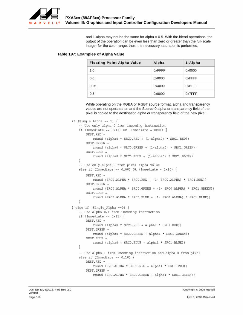
PXA3xx (88AP3xx) Processor FamilyVolume III: Graphics and Input Controller Configuration Developers Manual
Doc. No. MV-S301374-03 Rev. 2.0 Version -
Copyright © 2009 Marvell
Page 318 April 6, 2009 Released
12345678910111213141516171819202122232425262728293031323334353637383940414243444546474849505152535455565758
and 1-alpha may not be the same for alpha = 0.5. With the blend operations, the output of the operation can be even less than zero or greater than the full-scale integer for the color range, thus, the necessary saturation is performed.
While operating on the RGBA or RGBT source format, alpha and transparency values are not operated on and the Source 0 alpha or transparency field of the pixel is copied to the destination alpha or transparency field of the new pixel.
if (Single_Alpha == 1) {-- Use only alpha 0 from incoming instructionif (Immediate == 0x11) OR (Immediate = 0x01) {
DEST.RED = round (alpha0 * SRC0.RED + (1-alpha0) * SRC1.RED))
DEST.GREEN = round (alpha0 * SRC0.GREEN + (1-alpha0) * SRC1.GREEN))
DEST.BLUE = round (alpha0 * SRC0.BLUE + (1-alpha0) * SRC1.BLUE))
}-- Use only alpha 0 from pixel alpha valueelse if (Immediate == 0x00) OR (Immediate = 0x10) {
DEST.RED = round (SRC0.ALPHA * SRC0.RED + (1- SRC0.ALPHA) * SRC1.RED))
DEST.GREEN = round (SRC0.ALPHA * SRC0.GREEN + (1- SRC0.ALPHA) * SRC1.GREEN))
DEST.BLUE = round (SRC0.ALPHA * SRC0.BLUE + (1- SRC0.ALPHA) * SRC1.BLUE))
}
} else if (Single_Alpha ==0) {-- Use alpha 0/1 from incoming instructionif (Immediate == 0x11) {
DEST.RED = round (alpha0 * SRC0.RED + alpha1 * SRC1.RED))
DEST.GREEN = round (alpha0 * SRC0.GREEN + alpha1 * SRC1.GREEN))
DEST.BLUE = round (alpha0 * SRC0.BLUE + alpha1 * SRC1.BLUE))
}
-- Use alpha 1 from incoming instruction and alpha 0 from pixelelse if (Immediate == 0x10) {
DEST.RED = round (SRC.ALPHA * SRC0.RED + alpha1 * SRC1.RED))
DEST.GREEN = round (SRC.ALPHA * SRC0.GREEN + alpha1 * SRC1.GREEN))
Table 197: Examples of Alpha Value
Float ing Point Alpha Value Alpha 1-Alpha
1.0 0xFFFF 0x0000
0.0 0x0000 0xFFFF
0.25 0x4000 0xBFFF
0.5 0x8000 0x7FFF

Graphics ControllerGraphics Controller Instruction Set
Copyright © 2009 Marvell Doc. No. MV-S301374-03 Rev. 2.0Version -
April 6, 2009 Released Page 319
12345678910111213141516171819202122232425262728293031323334353637383940414243444546474849505152535455565758
DEST.BLUE = round (SRC.ALPHA * SRC0.BLUE + alpha1 * SRC1.BLUE))
}
-- Use alpha 0 from incoming instruction and alpha 1 from pixelelse if (Immediate == 0x01) {
DEST.RED = round (alpha0 * SRC0.RED + SRC1.ALPHA * SRC1.RED))
DEST.GREEN = round (alpha0 * SRC0.GREEN + SRC1.ALPHA * SRC1.GREEN))
DEST.BLUE = round (alpha0 * SRC0.BLUE + SRC1.ALPHA * SRC1.BLUE))
}
-- Use alpha 0/1 from pixel alpha valueelse if (Immediate == 0x00) {
DEST.RED = round (SRC0.ALPHA * SRC0.RED + SRC1.ALPHA * SRC1.RED))
DEST.GREEN = round (SRC0.ALPHA * SRC0.GREEN + SRC1.ALPHA * SRC1.GREEN))
DEST.BLUE = round (SRC0.ALPHA * SRC0.BLUE + SRC1.ALPHA * SRC1.BLUE))
}}
Exceptions No Raster Operations are supported for Alpha Blend BLT.
Clipping is not supported.
Encoding
Table 198: Alpha Blend BLT Instruction Encoding
GC Alpha Blend
Bit 31 30 29 28 27 26 25 24 23 22 21 20 19 18 17 16 15 14 13 12 11 10 9 8 7 6 5 4 3 2 1 0
GCI Type
Opcode Reserved
sin
gle
_a
lph
a
ble
nd
_o
p
imm Word Count
WD0 010 00111 0 x xx xx xxxx
WD1 Reserved DX0
WD2 Reserved DY0
WD3 Reserved S0X0
WD4 Reserved S0Y0
WD5 Reserved S1X0
WD6 Reserved S1Y0
WD7 Reserved Height Reserved Width

PXA3xx (88AP3xx) Processor FamilyVolume III: Graphics and Input Controller Configuration Developers Manual
Doc. No. MV-S301374-03 Rev. 2.0 Version -
Copyright © 2009 Marvell
Page 320 April 6, 2009 Released
12345678910111213141516171819202122232425262728293031323334353637383940414243444546474849505152535455565758
WD8 Alpha 0 (if imm(0) = 1) Alpha 1 (if imm(1) = 1)
WD0 Bits Name Descript ion
WD0 31:29 GCI Type 010 = 2-D graphics
28:24 Opcode 00111 = Alpha Blend BLT GC_ABLND
23:9 Reserved Reserved. Must be written as all zeros.
8 single_alpha 0 = Dual alpha 1 = Single alpha
7:6 Blend Op 00 = Add01 = Subtract (S0-S1)10 = Reverse subtract (S1-S0)11 = Reserved
5:4 Immediate 00 = Alpha values for both source 0 and source 1 are part of the input pixels.01 = Alpha value for source 0 is part of the incoming instruction, and the alpha value for source 1 is part of the input pixel.10 = Alpha value for source 0 is part of the input pixel, and the alpha value for source 1 is part of the incoming instruction.11 = Alpha values for both source 0 and source 1 are part of the incoming instruction.
3:0 Word Count Depends on imm. If imm = 00, the word count value is 0b0111. Otherwise, if imm != 00, the word count value is 0x1000.
WD1 Bits Name Descript ion
WD1 31:11 Reserved Reserved. Must be written as all zeros.
10:0 DX0 Starting pixel number of destination block
WD2 Bits Name Descript ion
WD2 31:11 Reserved Reserved. Must be written as all zeros.
10:0 DY0 Starting line number of destination block
WD3 Bits Name Descript ion
WD3 31:11 Reserved Reserved. Must be written as all zeros.
10:0 S0X0 Starting pixel number of source 0 block
WD4 Bits Name Descript ion
WD4 31:11 Reserved Reserved. Must be written as all zeros.
10:0 S0Y0 Starting line number of source 0 block
Table 198: Alpha Blend BLT Instruction Encoding (Continued)
GC Alpha Blend

Graphics ControllerGraphics Controller Instruction Set
Copyright © 2009 Marvell Doc. No. MV-S301374-03 Rev. 2.0Version -
April 6, 2009 Released Page 321
12345678910111213141516171819202122232425262728293031323334353637383940414243444546474849505152535455565758
4.6.2.8 Scale BLT
Overview Scales (multiplies) the image source using the RGBA alpha value as a scale factor or an immediate scale factor.
Figure 88: Scale BLT Operation
WD5 Bits Name Descript ion
WD5 31:11 Reserved Reserved. Must be written as all zeros.
10:0 S1X0 Starting pixel number of source 1 block
WD6 Bits Name Descript ion
WD6 31:11 Reserved Reserved. Must be written as all zeros.
10:0 S1Y0 Starting line number of source 1 block
WD7 Bits Name Descript ion
WD7 31:27 Reserved Reserved. Must be written as all zeros.
26:16 Height Positive Unsigned integer pixel height of the block
15:11 Reserved Reserved. Must be written as all zeros.
10:0 Width Positive unsigned integer pixel width of the block
WD8 Dependency Bits Name Descript ion
WD8 WD0:imm = 00 NA NA This WORD is not valid for this dependency condition.
WD0:imm(0) = 1 31:16 Alpha 0 16-bit Alpha for Source 0 (if immediate)
WD0:imm(1) = 1 15:0 Alpha 1 16-bit Alpha for Source 1 (if immediate)
Table 198: Alpha Blend BLT Instruction Encoding (Continued)
GC Alpha Blend
Source 0 Source 1 Destination (Before)
Destination (After)
* An “X” through a buffer means this buffer is not usedfor this instruction.
X
DX0DY0
SX0 Xscale factor =1.5
SY0

PXA3xx (88AP3xx) Processor FamilyVolume III: Graphics and Input Controller Configuration Developers Manual
Doc. No. MV-S301374-03 Rev. 2.0 Version -
Copyright © 2009 Marvell
Page 322 April 6, 2009 Released
12345678910111213141516171819202122232425262728293031323334353637383940414243444546474849505152535455565758
Usage GC_SCALE,<imm>,DX0, DY0, SX0, SY0, SCF
Qualifiers
Operation The Scale BLT instruction implements a scale (multiply) operation described by the following equation in its most simple form. If not immediate, the alpha value of the source 0 pixel is used as the scale factor. The scale factor is a 16-bit unsigned number with 8 integer bits and 8 fractional bits.
Note that this equation shows arithmetic operators, not logical operators.
The operation for the scale BLT can be captured as follows:
if (Immediate) {DEST.RED = round (scf * SRC0.RED);DEST.GREEN = round (scf * SRC0.GREEN);DEST.BLUE = round (scf * SRC0.BLUE);
} else {DEST.RED = round (SRC0.ALPHA * SRC0.RED);DEST.GREEN = round (SRC0.ALPHA * SRC0.GREEN);DEST.BLUE = round (SRC0.ALPHA * SRC0.BLUE);
}
Exceptions No Raster Operations are supported for Scale BLT.
Clipping is not supported.
Encoding
Qualif ier Descript ion
imm 0 = Input pixel contains scale factor as alpha component1 = 16-bit scale factor contained in incoming instruction
output source0 scf×=
Table 199: Scale BLT Instruction Encoding
GC Scale BLT
Bit 31 30 29 28 27 26 25 24 23 22 21 20 19 18 17 16 15 14 13 12 11 10 9 8 7 6 5 4 3 2 1 0
GCI Type
Opcode Reserved
imm Word
Count
WD0 010 01000 0 x xxxx
WD1 Reserved DX0
WD2 Reserved DY0
WD3 Reserved SX0

Graphics ControllerGraphics Controller Instruction Set
Copyright © 2009 Marvell Doc. No. MV-S301374-03 Rev. 2.0Version -
April 6, 2009 Released Page 323
12345678910111213141516171819202122232425262728293031323334353637383940414243444546474849505152535455565758
WD4 Reserved SY0
WD5 Reserved Height Reserved Width
WD6 Reserved Scale Factor (if imm = 1)
WD0 Bits Name Description
WD0 31:29 GCI Type 010 = 2-D graphics
28:24 Opcode 01000 = Scale BLT GC_SCALE
23:5 Reserved Reserved. Must be written as all zeros.
4 imm 0 = Scale Factor is located in the alpha portion of an RGBA pixel type1 = Scale Factor is supplied in the instruction stream
WD0 3:0 Word Count Depends on imm. If imm = 0, the word count value is 0b0101. Otherwise, if imm = 1, the value is 0b0110.
WD1 Bits Name Description
WD1 31:11 Reserved Reserved. Must be written as all zeros.
10:0 DX0 Starting pixel number of destination block
WD2 Bits Name Description
WD2 31:11 Reserved Reserved. Must be written as all zeros.
10:0 DY0 Starting line number of destination block
WD3 Bits Name Description
WD3 31:11 Reserved Reserved. Must be written as all zeros.
10:0 SX0 Starting pixel number of source 0 block
WD4 Bits Name Description
WD4 31:11 Reserved Reserved. Must be written as all zeros.
10:0 SY0 Starting line number of source 0 block
WD5 Bits Name Description
WD5 31:27 Reserved Reserved. Must be written as all zeros.
26:16 Height Positive Unsigned Integer Pixel Height of the Block
15:11 Reserved Reserved. Must be written as all zeros.
10:0 Width Positive Unsigned Integer Pixel Width of the Block
Table 199: Scale BLT Instruction Encoding (Continued)
GC Scale BLT

PXA3xx (88AP3xx) Processor FamilyVolume III: Graphics and Input Controller Configuration Developers Manual
Doc. No. MV-S301374-03 Rev. 2.0 Version -
Copyright © 2009 Marvell
Page 324 April 6, 2009 Released
12345678910111213141516171819202122232425262728293031323334353637383940414243444546474849505152535455565758
4.6.2.9 Bias BLT
Overview Biases (through addition) the image source using the RGBA alpha value as a bias factor or an immediate bias factor.
Figure 89: Bias BLT Operation
Usage GC_BIAS, <imm>, <op>, DX0, DY0, SX0, SY0, Width, Height, BIAS
Qualifiers
Operation Bias BLT implements a bias (add) operation described by the following equation in its most simple form. If not immediate, the alpha value in the source 0 pixel is used as the bias factor. If the output is saturated, it is clamped to 0xFFFF. If the output is underrun, it is clamped to 0x0000. The bias factor is a 16-bit unsigned integer number.
This equation shows arithmetic operators, not logical operators.
WD6 Dependency Bits Name Description
WD6 WD0:imm = 0 NA NA This WORD is not valid for this dependency condition.
WD0:imm = 1 31:16 Reserved Reserved. Must be written as all zeros.
15:0 Scale Scale factor (if immediate = 1). This is a 16-bit unsigned number with 8 integer bits and 8 fraction bits.
Table 199: Scale BLT Instruction Encoding (Continued)
GC Scale BLT
Source 0 Source 1 Destination (Before)
Destination (After)
* An “X” through a buffer means this buffer is not usedfor this instruction.
X
DX0DY0
SX0 Xbias factor = 10
SY0
OP
Quali f ier Descript ion
imm 0 = Input pixel contains bias factor as alpha component1 = 16-bit bias factor is part of incoming instruction

Graphics ControllerGraphics Controller Instruction Set
Copyright © 2009 Marvell Doc. No. MV-S301374-03 Rev. 2.0Version -
April 6, 2009 Released Page 325
12345678910111213141516171819202122232425262728293031323334353637383940414243444546474849505152535455565758
Bias BLT operation is as follows:
if (Immediate) {DEST.RED = round (bias + SRC0.RED);DEST.GREEN = round (bias + SRC0.GREEN);DEST.BLUE = round (bias + SRC0.BLUE);
} else {DEST.RED = round (SRC0.ALPHA + SRC0.RED);DEST.GREEN = round (SRC0.ALPHA + SRC0.GREEN);DEST.BLUE = round (SRC0.ALPHA + SRC0.BLUE);
}
Exceptions No Raster Operations are supported for Bias BLT.
Clipping is not supported.
Encoding
output source bias+=( )
Table 200: Bias Instruction Encoding
GC Bias
Bit 31 30 29 28 27 26 25 24 23 22 21 20 19 18 17 16 15 14 13 12 11 10 9 8 7 6 5 4 3 2 1 0
GCI Type
Opcode Reservedo
p
imm Word
Count
WD0 010 01001 0 x x xxxx
WD1 Reserved DX0
WD2 Reserved DY0
WD3 Reserved SX0
WD4 Reserved SY0
WD5 Reserved Height Reserved Width
WD6 Reserved Bias Factor (if imm = ‘1’)
WD0 Bits Name Descript ion

PXA3xx (88AP3xx) Processor FamilyVolume III: Graphics and Input Controller Configuration Developers Manual
Doc. No. MV-S301374-03 Rev. 2.0 Version -
Copyright © 2009 Marvell
Page 326 April 6, 2009 Released
12345678910111213141516171819202122232425262728293031323334353637383940414243444546474849505152535455565758
WD0 31:29 GCI Type 010 = 2-D graphics
28:24 Opcode 01001 = Bias BLT GC_BIAS
23:6 Reserved Reserved. Must be written as all zeros.
5 op 0 = Add Bias Factor and input pixel 1 = Subtract Bias Factor from input pixel
4 imm 0 = Bias Factor is located in the alpha portion of the input pixel 1 = Bias Factor is supplied in the instruction stream
3:0 Word Count Depends on imm. If imm = 0, the word count value is 0b0101. Otherwise, if imm = 1, the value is 0110.
WD1 Bits Name Descript ion
WD1 31:11 Reserved Reserved. Must be written as all zeros.
10:0 DX0 Starting pixel number of destination block
WD2 Bits Name Descript ion
WD2 31:11 Reserved Reserved. Must be written as all zeros.
10:0 DY0 Starting line number of destination block
WD3 Bits Name Descript ion
WD3 31:11 Reserved Reserved. Must be written as all zeros.
10:0 SX0 Starting pixel number of source 0 block
WD4 Bits Name Descript ion
WD4 31:11 Reserved Reserved. Must be written as all zeros.
10:0 SY0 Starting line number of source 0 block
WD5 Bits Name Descript ion
WD5 31:27 Reserved Reserved. Must be written as all zeros.
26:16 Height Positive Unsigned Integer Pixel Height of the Block
15:11 Reserved Reserved. Must be written as all zeros.
10:0 Width Positive Unsigned Integer Pixel Width of the Block
WD6 Dependency Bits Name Descript ion
Table 200: Bias Instruction Encoding (Continued)
GC Bias
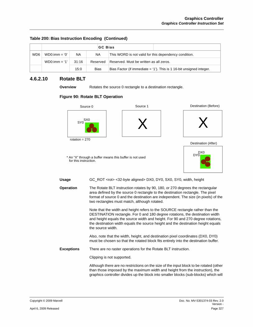
Graphics ControllerGraphics Controller Instruction Set
Copyright © 2009 Marvell Doc. No. MV-S301374-03 Rev. 2.0Version -
April 6, 2009 Released Page 327
12345678910111213141516171819202122232425262728293031323334353637383940414243444546474849505152535455565758
4.6.2.10 Rotate BLT
Overview Rotates the source 0 rectangle to a destination rectangle.
Figure 90: Rotate BLT Operation
Usage GC_ROT <rot> <32-byte aligned> DX0, DY0, SX0, SY0, width, height
Operation The Rotate BLT instruction rotates by 90, 180, or 270 degrees the rectangular area defined by the source 0 rectangle to the destination rectangle. The pixel format of source 0 and the destination are independent. The size (in pixels) of the two rectangles must match, although rotated.
Note that the width and height refers to the SOURCE rectangle rather than the DESTINATION rectangle. For 0 and 180 degree rotations, the destination width and height equals the source width and height. For 90 and 270 degree rotations, the destination width equals the source height and the destination height equals the source width.
Also, note that the width, height, and destination pixel coordinates (DX0, DY0) must be chosen so that the rotated block fits entirely into the destination buffer.
Exceptions There are no raster operations for the Rotate BLT instruction.
Clipping is not supported.
Although there are no restrictions on the size of the input block to be rotated (other than those imposed by the maximum width and height from the instruction), the graphics controller divides up the block into smaller blocks (sub-blocks) which will
WD6 WD0:imm = ‘0’ NA NA This WORD is not valid for this dependency condition.
WD0:imm = ‘1’ 31:16 Reserved Reserved. Must be written as all zeros.
15:0 Bias Bias Factor (if immediate = ‘1’). This is 1 16-bit unsigned integer.
Table 200: Bias Instruction Encoding (Continued)
GC Bias
Source 0 Source 1 Destination (Before)
Destination (After)
* An “X” through a buffer means this buffer is not usedfor this instruction.
X
DX0DY0
SX0
rotation = 270
XSY0

PXA3xx (88AP3xx) Processor FamilyVolume III: Graphics and Input Controller Configuration Developers Manual
Doc. No. MV-S301374-03 Rev. 2.0 Version -
Copyright © 2009 Marvell
Page 328 April 6, 2009 Released
12345678910111213141516171819202122232425262728293031323334353637383940414243444546474849505152535455565758
fit in the local scratchpad memory. Storage restrictions in the local scratchpad memory are based on the step size of the Source 0 buffer and are summarized in the table below.
Local scratchpad memory is used to optimize the performance of the rotation operation and saves internal bandwidth on System Bus 2.
The rotate instruction operates in two modes that are determined by the setting of the 32-byte aligned bit. When 32-byte aligned = 0, the starting addresses of the sub-blocks can have any alignment and the dimensions of the sub-blocks can be any size that fits into the local scratchpad memory. The performance of the rotate instruction when 32-byte aligned = 0 is degraded, but this mode offers the greatest flexibility in the choice of address and block size.
When 32-byte aligned = 1, the starting address of all sub-blocks must be 32-byte aligned and the dimensions of the sub-blocks are restricted. For the rotate instruction to work when 32-byte aligned = 1, the set of necessary and sufficient conditions in Table 217 must be true. Conforming to these constraints allows for 32-byte aligned operation, but it does not guarantee the best possible performance for the rotate instruction because Writes can still be unaligned. The performance is better than when 32-byte aligned = 0, but it is still not optimal.
To achieve the best performance, the constraints on the destination shown in Table 202 must also be met.
Table 201: Scratchpad Memory Usage for the Rotate BLT Instruction
Source 0 Step Size Maximum Size ( in Pixels) of Rotated Block
1 3065 pixels
2 1533 pixels
3 1020 pixels
4 767 pixels
8 384 pixels
Table 202: Additional Constraints for Best Performance in 32-byte Aligned Mode
Condit ions
1. Current GCDNBR(mod 32) = 0 where N = 0, 1, or 2.
2. Current GCDNSTR(mod 32) = 0 where N = 0, 1, or 2.
3. (DX0*Current GCDNSTP)(mod 32) = 0 where N = 0, 1, or 2. This constraint is satisfied by the following restrictions on DX0:a. DX0(mod 32) = 0 for GCDNSTP = 1.b. DX0(mod 16) = 0 for GCDNSTP = 2.c. DX0(mod 32) = 0 for GCDNSTP = 3.d. DX0(mod 8) = 0 for GCDNSTP = 4.e. DX0(mod 4) = 0 for GCDNSTP = 8.

Graphics ControllerGraphics Controller Instruction Set
Copyright © 2009 Marvell Doc. No. MV-S301374-03 Rev. 2.0Version -
April 6, 2009 Released Page 329
12345678910111213141516171819202122232425262728293031323334353637383940414243444546474849505152535455565758
When all constraints for the 32-byte aligned mode are met, all Reads and Writes from/to System Bus 2 have a byte count equal to the byte alignment of the address. Table 203 lists example register settings and instruction parameters that satisfy the necessary and sufficient conditions for achieving highest performance in 32-byte aligned mode.
Encoding
4. For 180 degree rotation, (width*Current GCDNSTP)(mod 32) = 0 where N = 0, 1, or 2. This constraint is satisfied by the following restrictions on width:a. width(mod 32) = 0 for GCDNSTP = 1.b. width(mod 16) = 0 for GCDNSTP = 2.c. width(mod 32) = 0 for GCDNSTP = 3.d. width(mod 8) = 0 for GCDNSTP = 4.e. width(mod 4) = 0 for GCDNSTP = 8.
5. For 90 degree and 270 degree rotations, (height*Current GCDNSTP)(mod 32) = 0 where N = 0, 1, or 2. This constraint is satisfied by the following restrictions on height:a. height(mod 32) = 0 for GCDNSTP = 1.b. height(mod 16) = 0 for GCDNSTP = 2.c. height(mod 32) = 0 for GCDNSTP = 3.d. height(mod 8) = 0 for GCDNSTP = 4.e. height(mod 4) = 0 for GCDNSTP = 8.
Table 203: Example Settings for 32-Byte Aligned = 1
Register Settings and Instruction Parameters
GCS0BR = 6496 (0x1960)
GCS0PF = 0 (1 byte per pixel)
GCS0STP = 1
GCS0STR = 640 (0x280)
S0X0 = 96 (0x60)
width = 544 (0x220)
height = 480 (0x1e0)
Current destination buffer = 0
GCD0PF = 0 (1 byte per pixel)
GCD0STP = 1
GCD0BR = 3424 (0xd60)
GCDSTR = 480 (0x1e0)
DX0 = 0
Table 202: Additional Constraints for Best Performance in 32-byte Aligned Mode
Condit ions

PXA3xx (88AP3xx) Processor FamilyVolume III: Graphics and Input Controller Configuration Developers Manual
Doc. No. MV-S301374-03 Rev. 2.0 Version -
Copyright © 2009 Marvell
Page 330 April 6, 2009 Released
12345678910111213141516171819202122232425262728293031323334353637383940414243444546474849505152535455565758
Table 204: Rotate BLT Instruction Encoding
GC Rotate BLT
Bit 31 30 29 28 27 26 25 24 23 22 21 20 19 18 17 16 15 14 13 12 11 10 9 8 7 6 5 4 3 2 1 0
GCI Type
Opcode Reserved 32b
Ro
tati
on Word
Count
WD0 010 01010 0 x xx 0101
WD1 Reserved DX0
WD2 Reserved DY0
WD3 Reserved SX0
WD4 Reserved SY0
WD5 Reserved Height Reserved Width
WD0 Bits Name Descript ion
WD0 31:29 GCI Type 010 = 2-D graphics
28:24 Opcode 01010 = Rotate BLT GC_ROT
23:7 Reserved Reserved. Must be written as all zeros.
6 32-byte aligned
0 = Block starting addresses are not 32-byte aligned1 = Block starting addresses are 32-byte aligned
5:4 Rotation Angle to rotate the source rectangle00 = No Rotation01 = Rotate by 90 degrees (clockwise)10 = Rotate by 180 degrees11 = Rotate by 270 degrees (90 degrees counter-clockwise)
3:0 Word Count 0b0101
WD1 Bits Name Descript ion
WD1 31:11 Reserved Reserved. Must be written as all zeros.
10:0 DX0 Starting pixel number of destination block
WD2 Bits Name Descript ion
WD2 31:11 Reserved Reserved. Must be written as all zeros.
10:0 DY0 Starting line number of destination block
WD3 Bits Name Descript ion
WD3 31:11 Reserved Reserved. Must be written as all zeros.
10:0 SX0 Starting pixel number of source 0 block

Graphics ControllerGraphics Controller Instruction Set
Copyright © 2009 Marvell Doc. No. MV-S301374-03 Rev. 2.0Version -
April 6, 2009 Released Page 331
12345678910111213141516171819202122232425262728293031323334353637383940414243444546474849505152535455565758
4.6.2.11 Raster Operation BLT
Overview Performs a bit-wise raster operation on source 0, source 1, and the destination, and stores the result in the destination. Using the raster opcode 0xCC, the Raster Operation BLT serves as the Source Copy BLT. Refer to Table 206 through Table 208 for information on the various raster opcodes.
Figure 91: Raster Operation BLT Operation
Usage GC_RAST<rop>DX0, DY0, S0X0, S0Y0, S1X0, S1Y0, width, height
Qualifiers
WD4 Bits Name Descript ion
WD4 31:11 Reserved Reserved. Must be written as all zeros.
10:0 SY0 Starting line number of source 0 block
WD5 Bits Name Descript ion
WD5 31:27 Reserved Reserved. Must be written as all zeros.
26:16 Height Positive unsigned integer pixel height of the block
15:11 Reserved Reserved. Must be written as all zeros.
10:0 Width Positive unsigned integer pixel width of the block
Table 204: Rotate BLT Instruction Encoding (Continued)
GC Rotate BLT
Quali f ier Description
rop Raster operation
Source 0 Source 1 Destination (Before)
Destination (After)
DX0DY0
S0X0 DX0DY0
** A Raster Operation is performed using Source 0,Source 1, and Destination.
rop**
S1X0S1Y0
S0Y0

PXA3xx (88AP3xx) Processor FamilyVolume III: Graphics and Input Controller Configuration Developers Manual
Doc. No. MV-S301374-03 Rev. 2.0 Version -
Copyright © 2009 Marvell
Page 332 April 6, 2009 Released
12345678910111213141516171819202122232425262728293031323334353637383940414243444546474849505152535455565758
Operation The Raster Operation BLT instruction performs a raster operation on the rectangular area defined by the source 0, source 1, and destination rectangles. It stores the result in the destination rectangle. The pixel formats of source 0, source 1, and the destination are independent. The size (in pixels) of the three rectangles must match.
Exceptions Clipping is not supported.
Encoding
Table 205: Raster Operation BLT Instruction Encoding
GC Raster BLT
Bit 31 30 29 28 27 26 25 24 23 22 21 20 19 18 17 16 15 14 13 12 11 10 9 8 7 6 5 4 3 2 1 0
GCI Type
Opcode Raster Op Reserved Word Count
WD0 010 01011 xxxxxxxx 0 0111
WD1 Reserved DX0
WD2 Reserved DY0
WD3 Reserved S0X0
WD4 Reserved S0Y0
WD5 Reserved S1X0
WD6 Reserved S1Y0
WD7 Reserved Height Reserved Width
WD0 Bits Name Descript ion
WD0 31:29 GCI Type 010 = 2-D graphics
28:24 Opcode 01011 = Raster BLT GC_RAST
23:16 Raster Op Raster Operation. Refer to Table 206 through Table 208 for information on the raster opcodes.
15:4 Reserved Reserved. Must be written as all zeros.
3:0 Word Count 0b0111
WD1 Bits Name Descript ion
WD1 31:11 Reserved Reserved. Must be written as all zeros.
10:0 DX0 Starting pixel number of destination block
WD2 Bits Name Descript ion
WD2 31:11 Reserved Reserved. Must be written as all zeros.
10:0 DY0 Starting line number of destination block

Graphics ControllerGraphics Controller Instruction Set
Copyright © 2009 Marvell Doc. No. MV-S301374-03 Rev. 2.0Version -
April 6, 2009 Released Page 333
12345678910111213141516171819202122232425262728293031323334353637383940414243444546474849505152535455565758
WD3 Bits Name Descript ion
WD3 31:11 Reserved Reserved. Must be written as all zeros.
10:0 S0X0 Starting pixel number of source 0 block
WD4 Bits Name Descript ion
WD4 31:11 Reserved Reserved. Must be written as all zeros.
10:0 S0Y0 Starting line number of source 0 block
WD5 Bits Name Descript ion
WD5 31:11 Reserved Reserved. Must be written as all zeros.
10:0 S1X0 Starting pixel number of source 1 block
WD6 Bits Name Descript ion
WD6 31:11 Reserved Reserved. Must be written as all zeros.
10:0 S1Y0 Starting line number of source 1 block
WD7 Bits Name Descript ion
WD7 31:27 Reserved Reserved. Must be written as all zeros.
26:16 Height Positive unsigned integer pixel height of the block
15:11 Reserved Reserved. Must be written as all zeros.
10:0 Width Positive unsigned integer pixel width of the block
Table 205: Raster Operation BLT Instruction Encoding (Continued)
GC Raster BLT
Table 206: Bit-Wise Operations and 8-bit Codes (40 – 7F)
Code Value Writ ten to Bits at Destinat ion
Code Value Writ ten to Bits at Destinat ion
40 S1 and (S0 and (not D)) 60 S1 and (D xor S0)
41 not (D or (S1 xor S0)) 61 not (D xor (S0 xor (S1 or (D and S0))))
42 (S0 xor D) and (S1 xor D) 62 D xor (S0 and (S1 or D))
43 not (S0 xor (S1 and (not (D and S0)))) 63 S0 xor (D or (not S1))
44 S0 and (not D) 64 S0 xor (D and (S1 or S0))
45 not (D or (S1 and (not S0))) 65 D xor (S0 or (not S1))

PXA3xx (88AP3xx) Processor FamilyVolume III: Graphics and Input Controller Configuration Developers Manual
Doc. No. MV-S301374-03 Rev. 2.0 Version -
Copyright © 2009 Marvell
Page 334 April 6, 2009 Released
12345678910111213141516171819202122232425262728293031323334353637383940414243444546474849505152535455565758
46 D xor (S0 or (S1 and D)) 66 D xor S0
47 not (S1 xor (S0 and (D xor S1))) 67 S0 xor (D or (not (S1 or S0)))
48 S0 and (D xor S1) 68 not (D xor (S0 xor (S1 or (not (D or S0)))))
49 not (S1 xor (D xor (S0 or (S1 and D)))) 69 not (S1 xor (D xor S0))
4A D xor (S1 and (S0 or D)) 6A D xor (S1 and S0)
4B S1 xor (D or (not S0)) 6B not (S1 xor (S0 xor (D and (S1 or S0))))
4C S0 and (not (D and S1)) 6C S0 xor (D and S1)
4D not (S0 xor ((S0 xor S1) or (D xor S0))) 6D not (S1 xor (D xor (S0 and (S1 or D))))
4E S1 xor (D or (S0 xor S1)) 6E S0 xor (D and (S1 or (not S0)))
4F not (S1 and (D or (not S0))) 6F not (S1 and (not (D xor S0)))
50 S1 and (not D) 70 S1 and (not (D and S0))
51 not (D or (S0 and (not S1))) 71 not (S0 xor ((S0 xor D) and (S1 xor D)))
52 D xor (S1 or (S0 and D)) 72 S0 xor (D or (S1 xor S0))
53 not (S0 xor (S1 and (D xor S0))) 73 not (S0 and (D or (not S1)))
54 not (D or (not (S1 or S0))) 74 D xor (S0 or (S1 xor D))
55 not D 75 not (D and (S0 or (not S1)))
56 D xor (S1 or S0) 76 S0 xor (D or (S1 and (not S0)))
57 not (D and (S1 or S0)) 77 not (D and S0)
58 S1 xor (D and (S0 or S1)) 78 S1 xor (D and S0)
59 D xor (S1 or (not S0)) 79 not (D xor (S0 xor (S1 and (D or S0))))
5A D xor S1 7A D xor (S1 and (S0 or (not D)))
5B D xor (S1 or (not (S0 or D))) 7B not (S0 and (not (D xor S1)))
5C D xor (S1 or (S0 xor D)) 7C S0 xor (S1 and (D or (not S0)))
5D not (D and (S1 or (not S0))) 7D not (D and (not (S1 xor S0)))
5E D xor (S1 or (S0 and (not D))) 7E (S0 xor S1) or (D xor S0)
5F not (D and S1) 7F not (D and (S1 and S0))
Note: Raster operations are performed using source 0, source 1, and destination as inputs.
Table 206: Bit-Wise Operations and 8-bit Codes (40 – 7F) (Continued)
Code Value Writ ten to Bits at Destinat ion
Code Value Writ ten to Bits at Destinat ion

Graphics ControllerGraphics Controller Instruction Set
Copyright © 2009 Marvell Doc. No. MV-S301374-03 Rev. 2.0Version -
April 6, 2009 Released Page 335
12345678910111213141516171819202122232425262728293031323334353637383940414243444546474849505152535455565758
Table 207: Bit-Wise Operations and 8-bit Codes (80 – BF)
Code Value Writ ten to Bits at Destinat ion
Code Value Writ ten to Bits at Dest inat ion
80 D and (S1 and S0) A0 D and S1
81 not ((S0 xor S1) or (D xor S0)) A1 not (S1 xor (D or (S0 and (not S1))))
82 D and (not (S1 xor S0)) A2 D and (S1 or (not S0))
83 not (S0 xor (S1 and (D or (not S0)))) A3 not (D xor (S1 or (S0 xor D)))
84 S0 and (not (D xor S1)) A4 not (S1 xor (D or (not (S0 or S1))))
85 not (S1 xor (D and (S0 or (not S1)))) A5 not (S1 xor D)
86 D xor (S0 xor (S1 and (D or S0))) A6 D xor (S0 and (not S1))
87 not (S1 xor (D and S0)) A7 not (S1 xor (D and (S0 or S1)))
88 D and S0 A8 D and (S1 or S0)
89 not (S0 xor (D or (S1 and (not S0)))) A9 not (D xor (S1 or S0))
8A D and (S0 or (not S1)) AA D
8B not (D xor (S0 or (S1 xor D))) AB D or (not (S1 or S0))
8C S0 and (D or (not S1)) AC S0 xor (S1 and (D xor S0))
8D not (S0 xor (D or (S1 xor S0))) AD not (D xor (S1 or (S0 and D)))
8E S0 xor ((S0 xor D) and (S1 xor D)) AE D or (S0 and (not S1))
8F not (S1 and (not (D and S0))) AF D or (not S1)
90 S1 and (not (D xor S0)) B0 S1 and (D or (not S0))
91 not (S0 xor (D and (S1 or (not S0)))) B1 not (S1 xor (D or (S0 xor S1)))
92 D xor (S1 xor (S0 and (D or S1))) B2 S0 xor ((S0 xor S1) or (D xor S0))
93 not (S0 xor (S1 and D)) B3 not (S0 and (not (D and S1)))
94 S1 xor (S0 xor (D and (S1 or S0))) B4 S1 xor (S0 and (not D))
95 not (D xor (S1 and S0)) B5 not (D xor (S1 and (S0 or D)))
96 D xor (S1 xor S0) B6 D xor (S1 xor (S0 or (D and S1)))
97 S1 xor (S0 xor (D or (not (S1 or S0)))) B7 not (S0 and (D xor S1))
98 not (S0 xor (D or (not (S1 or S0)))) B8 S1 xor (S0 and (D xor S1))
99 not (D xor S0) B9 not (D xor (S0 or (S1 and D)))
9A D xor (S1 and (not S0)) BA D or (S1 and (not S0))
9B not (S0 xor (D and (S1 or S0))) BB D or (not S0)
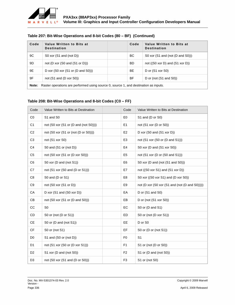
PXA3xx (88AP3xx) Processor FamilyVolume III: Graphics and Input Controller Configuration Developers Manual
Doc. No. MV-S301374-03 Rev. 2.0 Version -
Copyright © 2009 Marvell
Page 336 April 6, 2009 Released
12345678910111213141516171819202122232425262728293031323334353637383940414243444546474849505152535455565758
9C S0 xor (S1 and (not D)) BC S0 xor (S1 and (not (D and S0)))
9D not (D xor (S0 and (S1 or D))) BD not ((S0 xor D) and (S1 xor D))
9E D xor (S0 xor (S1 or (D and S0))) BE D or (S1 xor S0)
9F not (S1 and (D xor S0)) BF D or (not (S1 and S0))
Note: Raster operations are performed using source 0, source 1, and destination as inputs.
Table 207: Bit-Wise Operations and 8-bit Codes (80 – BF) (Continued)
Code Value Writ ten to Bits at Destinat ion
Code Value Writ ten to Bits at Dest inat ion
Table 208: Bit-Wise Operations and 8-bit Codes (C0 – FF)
Code Value Written to Bits at Destination Code Value Written to Bits at Destination
C0 S1 and S0 E0 S1 and (D or S0)
C1 not (S0 xor (S1 or (D and (not S0)))) E1 not (S1 xor (D or S0))
C2 not (S0 xor (S1 or (not (D or S0)))) E2 D xor (S0 and (S1 xor D))
C3 not (S1 xor S0) E3 not (S1 xor (S0 or (D and S1)))
C4 S0 and (S1 or (not D)) E4 S0 xor (D and (S1 xor S0))
C5 not (S0 xor (S1 or (D xor S0))) E5 not (S1 xor (D or (S0 and S1)))
C6 S0 xor (D and (not S1)) E6 S0 xor (D and (not (S1 and S0)))
C7 not (S1 xor (S0 and (D or S1))) E7 not ((S0 xor S1) and (S1 xor D))
C8 S0 and (D or S1) E8 S0 xor ((S0 xor S1) and (D xor S0))
C9 not (S0 xor (S1 or D)) E9 not (D xor (S0 xor (S1 and (not (D and S0)))))
CA D xor (S1 and (S0 xor D)) EA D or (S1 and S0)
CB not (S0 xor (S1 or (D and S0))) EB D or (not (S1 xor S0))
CC S0 EC S0 or (D and S1)
CD S0 or (not (D or S1)) ED S0 or (not (D xor S1))
CE S0 or (D and (not S1)) EE D or S0
CF S0 or (not S1) EF S0 or (D or (not S1))
D0 S1 and (S0 or (not D)) F0 S1
D1 not (S1 xor (S0 or (D xor S1))) F1 S1 or (not (D or S0))
D2 S1 xor (D and (not S0)) F2 S1 or (D and (not S0))
D3 not (S0 xor (S1 and (D or S0))) F3 S1 or (not S0)

Graphics ControllerGraphics Controller Instruction Set
Copyright © 2009 Marvell Doc. No. MV-S301374-03 Rev. 2.0Version -
April 6, 2009 Released Page 337
12345678910111213141516171819202122232425262728293031323334353637383940414243444546474849505152535455565758
4.6.2.12 Pattern Copy BLT
Overview The Pattern Copy BLT Instruction has two modes of operation.
• Option 1 replicates a rectangular block of data from source 0 repeatedly in the destination buffer.
• Option 2 streams a block of data out linearly (useful for texture patterns when the output should look random).
Figure 92: Pattern Copy BLT Operation Option 1
D4 S0 xor ((S0 xor S1) and (S1 xor D)) F4 S1 or (S0 and (not D))
D5 not (D and (not (S1 and S0))) F5 S1 or (not D)
D6 S1 xor (S0 xor (D or (S1 and S0))) F6 S1 or (D xor S0)
D7 not (D and (S1 xor S0)) F7 S1 or (not (D and S0))
D8 S1 xor (D and (S0 xor S1)) F8 S1 or (D and S0)
D9 not (S0 xor (D or (S1 and S0))) F9 S1 or (not (D xor S0))
DA D xor (S1 and (not (S0 and D))) FA D or S1
DB not ((S0 xor S1) and (D xor S0)) FB D or (S1 or (not S0))
DC S0 or (S1 and (not D)) FC S1 or S0
DD S0 or (not D) FD S1 or (S0 or (not D))
DE S0 or (D xor S1) FE D or (S1 or S0)
DF S0 or (not (D and S1)) FF write D all 1’s
Note: Raster operations are performed using source 0, source 1, and destination as inputs.
Table 208: Bit-Wise Operations and 8-bit Codes (C0 – FF) (Continued)
Code Value Written to Bits at Destination Code Value Written to Bits at Destination
Source 0 Source 1 Destination (Before)
Destination (After)
* An “X” through a buffer means this buffer is not usedfor this instruction.
X
DX0DY0
SX0 XSY0

PXA3xx (88AP3xx) Processor FamilyVolume III: Graphics and Input Controller Configuration Developers Manual
Doc. No. MV-S301374-03 Rev. 2.0 Version -
Copyright © 2009 Marvell
Page 338 April 6, 2009 Released
12345678910111213141516171819202122232425262728293031323334353637383940414243444546474849505152535455565758
Figure 93: Pattern Copy BLT Operation Option 2
Usage GC_PATT <opt> DX0, DY0, SX0, SX0, S_width, S_height, D_width, D_height
Qualifiers None
Operation The destination rectangle is defined by the DX0 and DY0 pixel numbers and the D_width and D_height dimensions. The source 0 pattern is defined by the SX0 and SY0 pixel numbers and the S_width and S_height dimensions
The source pattern is copied as many times as required to the destination rectangle. No stretching is involved.
Description The pattern copy operates correctly for a source pattern block size which fits into the internal scratchpad memory of the graphics controller. The operations for Option 1 and Option 2 are as follows. For both, the SRC0 input pattern is read in to the local scratchpad memory (SCH).
Option 1:
dy=DY0loop2: while (dy LE DY1)
dx = DX0loop1 : while (dx LE. DX1)
DEST(dx, dy) = SCH (SX0 + dx mod(SX1-SX0+1), SY0 + dy mod(SY1-SY0+1))
dx = dx+1end loop 1
dy= dy+1end loop2
Option 2:
dy=DY0s_count=0loop2: while (dy LE DY1)
dx = DX0loop1 : while (dx LE. DX1)
Source 0 Source 1 Destination (Before)
Destination (After)
* An “X” through a buffer means this buffer is not usedfor this instruction.
X
DX0DY0
SX0 XSY0

Graphics ControllerGraphics Controller Instruction Set
Copyright © 2009 Marvell Doc. No. MV-S301374-03 Rev. 2.0Version -
April 6, 2009 Released Page 339
12345678910111213141516171819202122232425262728293031323334353637383940414243444546474849505152535455565758
DEST(dx, dy) = SCH (s_count)dx = dx+1if (s_count LE s_width * s_height)
s_count=0;else
s_count=s_count+1;
end loop 1dy= dy+1end loop2
Exceptions Pattern Copy BLT does not support Raster Operations.
Clipping is not supported.
Storage restrictions in the local scratchpad memory are computed using the following restrictions. The entire pattern is read into local memory and then the fill is performed. Thus, the entire pattern must fit into local memory. These restrictions must be maintained for correct performance of the graphics controller. The size of the pattern is defined by the following equation:
X = # pixels per line in patternB = # of bytes to fetch extra per line of blockY = # lines per patternS = step size
Therefore, the size of the pattern must satisfy the following formula:
CEIL(((S*X)+B)/8) * Y <= 384
Encoding
Table 209: Pattern Copy BLT Instruction Encoding
GC Pattern Copy BLT
Bit 31 30 29 28 27 26 25 24 23 22 21 20 19 18 17 16 15 14 13 12 11 10 9 8 7 6 5 4 3 2 1 0
GCI Type
Opcode Reserved
op
t Word Count
WD0 010 01100 0 x 0110
WD1 Reserved DX0
WD2 Reserved DY0
WD3 Reserved SX0
WD4 Reserved SY0
WD5 Reserved S_Height Reserved S_Width
WD6 Reserved D_Height Reserved D_Width
WD0 Bits Name Descript ion

PXA3xx (88AP3xx) Processor FamilyVolume III: Graphics and Input Controller Configuration Developers Manual
Doc. No. MV-S301374-03 Rev. 2.0 Version -
Copyright © 2009 Marvell
Page 340 April 6, 2009 Released
12345678910111213141516171819202122232425262728293031323334353637383940414243444546474849505152535455565758
WD0 31:29 GCI Type 010 = 2-D graphics
28:24 Opcode 01100 = Pattern Copy BLT GC_PATT
23:5 Reserved Reserved. Must be written as all zeros.
4 option 0 = Use Option 1. Replicate a block multiple times from a source to a destination.1 = Use Option 2. Linearly fill in a destination area with a stream of data.
3:0 Word Count 0b0110
WD1 Bits Name Descript ion
WD1 31:11 Reserved Reserved. Must be written as all zeros.
10:0 DX0 Starting pixel number of destination block
WD2 Bits Name Descript ion
WD2 31:11 Reserved Reserved. Must be written as all zeros.
10:0 DY0 Starting line number of destination block
WD3 Bits Name Descript ion
WD3 31:11 Reserved Reserved. Must be written as all zeros.
10:0 SX0 Starting pixel number of source 0 block
WD4 Bits Name Descript ion
WD4 31:11 Reserved Reserved. Must be written as all zeros.
10:0 SY0 Starting line number of source 0 block
WD5 Bits Name Descript ion
WD5 31:27 Reserved Reserved. Must be written as all zeros.
26:16 S_Height Positive Unsigned Integer Pixel Height of the Source Block
15:11 Reserved Reserved. Must be written as all zeros.
10:0 S_Width Positive Unsigned Integer Pixel Width of the Source Block
WD6 Bits Name Descript ion
WD6 31:27 Reserved Reserved. Must be written as all zeros.
26:16 D_Height Positive Unsigned Integer Pixel Height of the Destination Block
15:11 Reserved Reserved. Must be written as all zeros.
10:0 D_Width Positive Unsigned Integer Pixel Width of the Destination Block
Table 209: Pattern Copy BLT Instruction Encoding (Continued)
GC Pattern Copy BLT

Graphics ControllerGraphics Controller Instruction Set
Copyright © 2009 Marvell Doc. No. MV-S301374-03 Rev. 2.0Version -
April 6, 2009 Released Page 341
12345678910111213141516171819202122232425262728293031323334353637383940414243444546474849505152535455565758
4.6.2.13 Decimate BLT
Overview Reduces a rectangular block of data using a bilinear decimation. One extra pixel per source line and one extra line per source block are read from memory. See Section 4.5.9, Reading Extra Pixels, on page 272.
Figure 94: Decimate BLT Operation
Usage GC_DECBLT DX0, DY0, SX0, SY0, S_width, S_height, D_width, D_height, X_dec_int, X_dec_frac, Y_dec_int, Y_dec_frac
Qualifiers None
Operation The decimation operation can be performed in any direction for integer (for example, 1 in every 3 pixels) and non-integer types (for example, 1 in every 3.5 pixels) of decimating. However, the intended decimation must be less than or equal to one. If a decimation greater than 1 is required, this is actually a stretch and the Stretch BLT instruction must be used (See Section 4.6.2.6, Stretch BLT, on page 312).
You must program a sub-decimate factor for both the X dimension (X_dec_int.X_dec_frac) and the Y dimension (Y_dec_int.Y_dec_frac). The X_dec_int, X_dec_frac, and Y_dec_int, Y_dec_frac values are each 10-bit unsigned numbers and are calculated as follows:
X_dec_int.X_dec_frac = (Source_0_width-1)/(Destination_width-1)Y_dec_int.Y_dec_frac = (Source_0_height-1)/(Destination_height-1)
Note
Note The X_dec_frac and Y_dec_frac values should be truncated to 10-bits.
Exceptions If the destination width (height) is equal to the source width (height), then
x(y)_dec_int.x(y)_dec_frac = 000.3FFh
If the destination width (height) is 1 and the source width (height) is not 1, the result is a divide by 0 operation:
Source 0 Source 1 Destination (Before)
Destination (After)
* An “X” through a buffer means this buffer is not usedfor this instruction.
X
DX0DY0
SX0 XSY0

PXA3xx (88AP3xx) Processor FamilyVolume III: Graphics and Input Controller Configuration Developers Manual
Doc. No. MV-S301374-03 Rev. 2.0 Version -
Copyright © 2009 Marvell
Page 342 April 6, 2009 Released
12345678910111213141516171819202122232425262728293031323334353637383940414243444546474849505152535455565758
x(y)_dec_int.x(y)_dec_frac = 001.000h
If the source width (height) is 1 and the destination width (height) is not 1, this is actually a stretch in this direction, and the programmed value should be
x(y)_dec_int.x(y)_dec_frac = 000.000h
Four pixels are used to generate a new pixel. Decimation is performed on the red, green, blue, and alpha components to generate the new pixel.
Table 210 shows examples of the X_dec_int.X_dec_frac and Y_dec_int.Y_dec_frac decimations. These are 20-bit unsigned values with 10 integer bits and 10 fraction bits.
Exceptions Decimate BLT does not support Raster Operations.
Clipping is not supported.
You must ensure that programming for the X_dec and Y_dec integer and fractional values is consistent with that for the source and destination width and height values. The graphics controller does not double-check the values. Invalid results occur if the values written by software are inconsistent.
Storage restrictions in the local scratchpad memory are based on the input pixel format and step size of the source 0 buffer and are summarized in Table 211. These restrictions must be maintained for correct performance.
Table 210: Examples of X_dec and Y_dec values
SourceWidth
Destinat ionWidth
X_decValue
X_decProgrammed
SourceHeight
Destinat ionHeight
Y_decValue
Y_decProgrammed
10 5 9/4 0000000010.0100000000
18 7 17/6 0000000010.1101010101
20 3 19/2 0000001001.1000000000
32 5 31/4 0000000111.1100000000
256 25 255/24 0000001010.1010000000
250 10 249/9 0000011011.1010101010
100 99 99/98 0000000001.0000001010
221 100 220/99 0000000010.0011100011

Graphics ControllerGraphics Controller Instruction Set
Copyright © 2009 Marvell Doc. No. MV-S301374-03 Rev. 2.0Version -
April 6, 2009 Released Page 343
12345678910111213141516171819202122232425262728293031323334353637383940414243444546474849505152535455565758
Encoding
Table 211: Source 0 Block Width Restrictions for Decimate BLT Instruction
Source 0Step Size
Max Width ( in pixels) of Source 0 Block
1 497 pixels
2 249 pixels
3 167 pixels
4 126 pixels
8 63 pixels
Table 212: Bit-Wise Operations and 8-bit Codes (00 – 3F)
Code Value Written to Bits at Dest ination
Code Value Written to Bits at Dest ination
00 write D all 0’s 20 D and (S1 and (not S0))
01 not (D or (S1 or S0))) 21 not (S0 or (D xor S1))
02 D and (not (S1 or S0)) 22 D and (not S0)
03 not (S1 or S0) 23 not (S0 or (S1 and (not D)))
04 S0 and (not (D or S1)) 24 (S0 xor S1) and (D xor S0)
05 not (D or S1) 25 not (S1 xor (D and (not (S0 and S1))))
06 not (S1 or (not (D xor S0))) 26 S0 xor (D or (S1 and S0))
07 not (S1 or (D and S0)) 27 S0 xor (D or (not (S1 xor S0)))
08 S0 and (D and (not S1)) 28 D and (S1 xor S0)
09 not (S1 or (D xor S0)) 29 not (S1 xor (S0 xor (D or (S1 and S0))))
0A D and (not S1) 2A D and (not (S1 and S0))
0B not (S1 or (S0 and (not D))) 2B not (S0 xor ((S0 xor S1) and (S1 xor D)))
0C S0 and (not S1) 2C S0 xor (S1 and (D or S0))
0D not (S1 or (D and (not S0))) 2D S1 xor (S0 or (not D))
0E not (S1 or (not (D or S0))) 2E S1 xor (S0 or (D xor S1))
0F not S1 2F not (S1 and (S0 or (not D)))
10 S1 and (not (D or S0)) 30 S1 and (not S0)

PXA3xx (88AP3xx) Processor FamilyVolume III: Graphics and Input Controller Configuration Developers Manual
Doc. No. MV-S301374-03 Rev. 2.0 Version -
Copyright © 2009 Marvell
Page 344 April 6, 2009 Released
12345678910111213141516171819202122232425262728293031323334353637383940414243444546474849505152535455565758
4.7 Register Descriptions
4.7.0.1 Register SummaryTable 213 shows the graphics controller registers and the physical addresses to access them. These registers must be mapped as non-cacheable and non-bufferable, and they can only be accessed as word accesses (32-bits). They are grouped together within one page and thus all have the same memory protections. For easy reference, the summary table includes the page number of the detailed description for each register. The remainder of this section describes the individual registers in detail.
11 not (D or S0) 31 not (S0 or (D and (not S1)))
12 not (S0 or (not (D xor S1))) 32 S0 xor (D or (S1 or S0))
13 not (S0 or (D and S1)) 33 not S0
14 not (D or (not (S1 xor S0))) 34 S0 xor (S1 or (D and S0))
15 not (D or (S1 and S0)) 35 S0 xor (S1 or (not (D xor S0)))
16 S1 xor (S0 xor (D and (not (S1 and S0))))
36 S0 xor (D or S1)
17 not (S0 xor ((S0 xor S1) and (D xor S0)))
37 not (S0 and (D or S1))
18 (S0 xor S1) and (S1 xor D) 38 S1 xor (S0 and (D or S1))
19 not (S0 xor (D and (not (S1 and S0)))) 39 S0 xor (S1 or (not D))
1A S1 xor (D or (S0 and S1)) 3A S0 xor (S1 or (D xor S0))
1B not (S0 xor (D and (S1 xor S0))) 3B not (S0 and (S1 or (not D)))
1C S1 xor (S0 or (D and S1)) 3C S1 xor S0
1D not (D xor (S0 and (S1 xor D))) 3D S0 xor (S1 or (not (D or S0)))
1E S1 xor (D or S0) 3E S0 xor (S1 or (D and (not S0)))
1F not (S1 and (D or S0)) 3F not (S1 and S0)
Note: Raster Operations are performed using Source 0, Source 1, and Destination as inputs.
Table 212: Bit-Wise Operations and 8-bit Codes (00 – 3F)
Code Value Written to Bits at Dest ination
Code Value Written to Bits at Dest ination
Table 213: Graphics Controller Registers
Physical Address
Register Name Page
Miscellaneous Control and Interrupt Information

Graphics ControllerRegister Descriptions
Copyright © 2009 Marvell Doc. No. MV-S301374-03 Rev. 2.0Version -
April 6, 2009 Released Page 345
12345678910111213141516171819202122232425262728293031323334353637383940414243444546474849505152535455565758
0x5400_0000 Graphics Controller Configuration Register (GCCR) page 348
0x5400_0004 Graphics Controller Interrupt Status Control Register (GCISCR) page 350
0x5400_0008 Graphics Controller Interrupt Enable Control Register (GCIECR) page 352
0x5400_000C Graphics Controller NOP ID Register (GCNOPID) page 354
0x5400_0010 Graphics Controller Default Alpha Setting Register (GCALPHASET)
page 355
0x5400_0014 Graphics Controller Default Transparency Setting Register (GCTSET)
page 356
0x5400_0018 –0x5400_001C
Reserved —
Ring Buffer Information
0x5400_0020 Graphics Controller Ring Buffer Base Address Register (GCRBBR)
page 357
0x5400_0024 Graphics Controller Ring Buffer Length Register (GCRBLR) page 357
0x5400_0028 Graphics Controller Ring Buffer Head Register (GCRBHR) page 358
0x5400_002C Graphics Controller Ring Buffer Tail Register (GCRBTR) page 358
0x5400_0030 Graphics Controller Ring Buffer Execution Head Register (GCRBEXHR)
page 359
0x5400_0034–0x5400_003C
Reserved —
Batch Buffer Information
0x5400_0040 Graphics Controller Batch Buffer Base Address Register (GCBBBR)
page 359
0x540_0044 Graphics Controller Batch Buffer Head Register (GCBBHR) page 360
0x5400_0048 Graphics Controller Batch Buffer Execution Head Register (GCBBEXHR)
page 360
0x5400_004C–0x5400_005C
Reserved —
Destination 0 Information
0x5400_0060 Graphics Controller Destination Buffer 0 (Display Buffer 0) Base Address Register (GCD0BR)
page 361
0x5400_0064 Graphics Controller Destination Buffer 0 (Display Buffer 0) Step Size Register (GCD0STP)
page 361
Table 213: Graphics Controller Registers (Continued)
Physical Address
Register Name Page

PXA3xx (88AP3xx) Processor FamilyVolume III: Graphics and Input Controller Configuration Developers Manual
Doc. No. MV-S301374-03 Rev. 2.0 Version -
Copyright © 2009 Marvell
Page 346 April 6, 2009 Released
12345678910111213141516171819202122232425262728293031323334353637383940414243444546474849505152535455565758
0x5400_0068 Graphics Controller Destination Buffer 0 (Display Buffer 0) Stride Size Register (GCD0STR)
page 362
0x5400_006C Graphics Controller Destination Buffer 0 (Display Buffer 0) Pixel Format Register (GCD0PF)
page 362
Destination 1 Information
0x5400_0070 Graphics Controller Destination Buffer 1 (Display Buffer 1) Base Address Register (GCD1BR)
page 363
0x5400_0074 Graphics Controller Destination Buffer 1 (Display Buffer 1) Step Size Register (GCD1STP)
page 363
0x5400_0078 Graphics Controller Destination Buffer 1 (Display Buffer 1) Stride Size Register (GCD1STR)
page 364
0x5400_007C Graphics Controller Destination Buffer 1 (Display Buffer 1) Pixel Format Register (GCD1PF)
page 364
Destination 2 Information
0x5400_0080 Graphics Controller Destination Buffer 2 Base Address Register (GCD2BR)
page 365
0x5400_0084 Graphics Controller Destination Buffer 2 Step Size Register (GCD2STP)
page 365
0x5400_0088 Graphics Controller Destination Buffer 2 Stride Size Register (GCD2STR)
page 366
0x5400_008C Graphics Controller Destination Buffer 2 Pixel Format Register (GCD2PF)
page 366
0x5400_0090–0x5400_00DC
Reserved —
Source 0 Information
0x5400_00E0 Graphics Controller Source 0 Base Address Register (GCS0BR) page 367
0x5400_00E4 Graphics Controller Source 0 Step Size Register (GCS0STP) page 367
0x5400_00E8 Graphics Controller Source 0 Stride Size Register (GCS0STR) page 368
0x5400_00EC Graphics Controller Source 0 Pixel Format Register (GCS0PF) page 368
Source 1 Information
0x5400_00F0 Graphics Controller Source 1 Base Address Register (GCS1BR) page 369
0x5400_00F4 Graphics Controller Source 1 Step Size Register (GCS1STP) page 369
0x5400_00F8 Graphics Controller Source 1 Stride Size Register (GCS1STR) page 370
0x5400_00FC Graphics Controller Source 1 Pixel Format Register (GCS1PF)
Table 213: Graphics Controller Registers (Continued)
Physical Address
Register Name Page

Graphics ControllerRegister Descriptions
Copyright © 2009 Marvell Doc. No. MV-S301374-03 Rev. 2.0Version -
April 6, 2009 Released Page 347
12345678910111213141516171819202122232425262728293031323334353637383940414243444546474849505152535455565758
0x5400_0100–0x5400_015C
Reserved —
Pixel ALU Scratch Registers
0x5400_0160 Graphics Controller Pixel ALU Scratch register 0 Word 0 (GCSC0WD0)
page 370
0x5400_0164 Graphics Controller Pixel ALU Scratch register 0 Word 1 (GCSC0WD1)
page 371
0x5400_0168 Graphics Controller Pixel ALU Scratch register 1 Word 0 (GCSC1WD0)
page 371
0x5400_016C Graphics Controller Pixel ALU Scratch register 1 Word 0 (GCSC1WD1)
page 371
0x5400_0170 Graphics Controller Pixel ALU Scratch register 2 Word 0 (GCSC2WD0)
page 371
0x5400_0174 Graphics Controller Pixel ALU Scratch register 2 Word 1 (GCSC2WD1)
page 371
0x5400_0178 Graphics Controller Pixel ALU Scratch register 3 Word 0 (GCSC3WD0)
page 371
0x5400_017C Graphics Controller Pixel ALU Scratch register 3 Word 1 (GCSC3WD1)
page 371
0x5400_0180 Graphics Controller Pixel ALU Scratch register 4 Word 0 (GCSC4WD0)
page 371
0x5400_0184 Graphics Controller Pixel ALU Scratch register 4 Word 1 (GCSC4WD1)
page 371
0x5400_0188 Graphics Controller Pixel ALU Scratch register 5 Word 0 (GCSC5WD0)
page 371
0x5400_018C Graphics Controller Pixel ALU Scratch register 5 Word 1 (GCSC5WD1)
page 371
0x5400_0190 Graphics Controller Pixel ALU Scratch register 6 Word 0 (GCSC6WD0)
page 371
0x5400_0194 Graphics Controller Pixel ALU Scratch register 6 Word 1 (GCSC6WD1)
page 371
0x5400_0198 Graphics Controller Pixel ALU Scratch register 7 Word 0 (GCSC7WD0)
page 371
0x5400_019C Graphics Controller Pixel ALU Scratch register 7 Word 1 (GCSC7WD1)
page 371
Table 213: Graphics Controller Registers (Continued)
Physical Address
Register Name Page
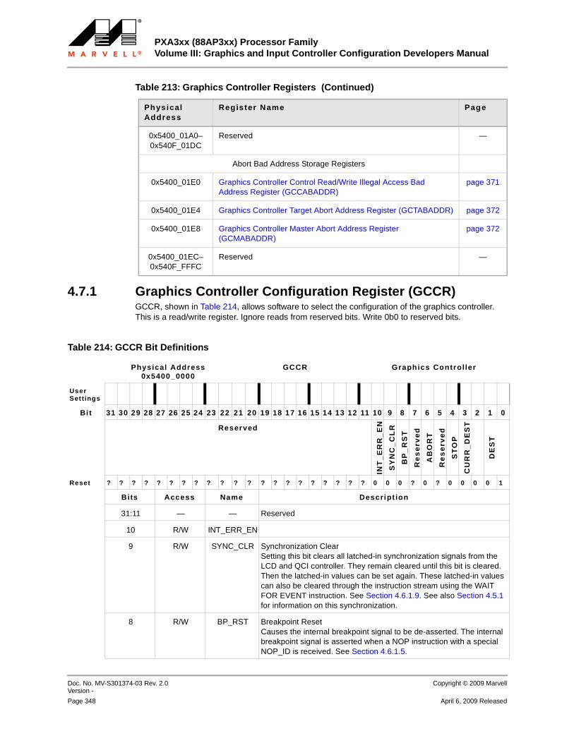
PXA3xx (88AP3xx) Processor FamilyVolume III: Graphics and Input Controller Configuration Developers Manual
Doc. No. MV-S301374-03 Rev. 2.0 Version -
Copyright © 2009 Marvell
Page 348 April 6, 2009 Released
12345678910111213141516171819202122232425262728293031323334353637383940414243444546474849505152535455565758
4.7.1 Graphics Controller Configuration Register (GCCR)GCCR, shown in Table 214, allows software to select the configuration of the graphics controller. This is a read/write register. Ignore reads from reserved bits. Write 0b0 to reserved bits.
0x5400_01A0–0x540F_01DC
Reserved —
Abort Bad Address Storage Registers
0x5400_01E0 Graphics Controller Control Read/Write Illegal Access Bad Address Register (GCCABADDR)
page 371
0x5400_01E4 Graphics Controller Target Abort Address Register (GCTABADDR) page 372
0x5400_01E8 Graphics Controller Master Abort Address Register (GCMABADDR)
page 372
0x5400_01EC–0x540F_FFFC
Reserved —
Table 213: Graphics Controller Registers (Continued)
Physical Address
Register Name Page
Table 214: GCCR Bit Definitions
Physical Address0x5400_0000
GCCR Graphics Controller
User Settings
Bit 31 30 29 28 27 26 25 24 23 22 21 20 19 18 17 16 15 14 13 12 11 10 9 8 7 6 5 4 3 2 1 0
Reserved
INT
_E
RR
_E
N
SY
NC
_C
LR
BP
_R
ST
Re
se
rve
d
AB
OR
T
Re
se
rve
d
ST
OP
CU
RR
_D
ES
T
DE
ST
Reset ? ? ? ? ? ? ? ? ? ? ? ? ? ? ? ? ? ? ? ? ? 0 0 0 ? 0 ? 0 0 0 0 1
Bits Access Name Descript ion
31:11 — — Reserved
10 R/W INT_ERR_EN
9 R/W SYNC_CLR Synchronization ClearSetting this bit clears all latched-in synchronization signals from the LCD and QCI controller. They remain cleared until this bit is cleared. Then the latched-in values can be set again. These latched-in values can also be cleared through the instruction stream using the WAIT FOR EVENT instruction. See Section 4.6.1.9. See also Section 4.5.1 for information on this synchronization.
8 R/W BP_RST Breakpoint ResetCauses the internal breakpoint signal to be de-asserted. The internal breakpoint signal is asserted when a NOP instruction with a special NOP_ID is received. See Section 4.6.1.5.

Graphics ControllerRegister Descriptions
Copyright © 2009 Marvell Doc. No. MV-S301374-03 Rev. 2.0Version -
April 6, 2009 Released Page 349
12345678910111213141516171819202122232425262728293031323334353637383940414243444546474849505152535455565758
7 — — Reserved
6 R/W ABORT AbortAborts all current activity in the 2-D graphics engine. Setting this bit causes all instructions to be flushed from the ring and batch buffers and any currently executing instruction to stop. It also resets the ring buffer control registers. No execution resumes until this bit is cleared and the ring buffer is reprogrammed. ABORT must be cleared for the ring buffer to be reprogrammed. System bus 2 still accepts control register Reads and Writes while this bit is set, but the ring buffer control registers cannot be written and System Bus 2 Writes are discarded.
5 — — Reserved
4 R/W STOP StopHalts the 2-D graphics engine. Setting this bit causes the 2-D Graphics Engine to finish the current instruction and then stop all activity until this bit is cleared. Ring and batch buffer contexts are maintained, and if space in available internally, accesses for these buffer contents can still occur on System Bus 2. System bus 2 still accepts control register Reads and Writes while this bit is asserted. Once stopped, GCISCR[STOP_INTST] is set and an interrupt request is generated if it is enabled.
3:2 R/W CURR_DEST Current Destination BufferContains the number of the current destination buffer and can be updated by the Destination Buffer Flip instruction. See Section 4.6.1.6. If DEST is programmed to use only Destination Buffer 2, this field must be programmed with Destination Buffer 2. If it is not, it is forced to be Destination Buffer 2. If DEST is programmed to use destination buffers 0 and 1, this field must be programmed for these buffers. If it is not, it is forced to be Destination Buffer 0.0b00 = Destination buffer 0 (Display Buffer 0)0b01 = Destination buffer 1 (Display Buffer 1)0b10 = Destination buffer 20b11 = Reserved
Table 214: GCCR Bit Definitions (Continued)
Physical Address0x5400_0000
GCCR Graphics Controller
User Settings
Bit 31 30 29 28 27 26 25 24 23 22 21 20 19 18 17 16 15 14 13 12 11 10 9 8 7 6 5 4 3 2 1 0
Reserved
INT
_E
RR
_E
N
SY
NC
_C
LR
BP
_R
ST
Re
se
rve
d
AB
OR
T
Re
se
rve
d
ST
OP
CU
RR
_D
ES
T
DE
ST
Reset ? ? ? ? ? ? ? ? ? ? ? ? ? ? ? ? ? ? ? ? ? 0 0 0 ? 0 ? 0 0 0 0 1
Bits Access Name Descript ion
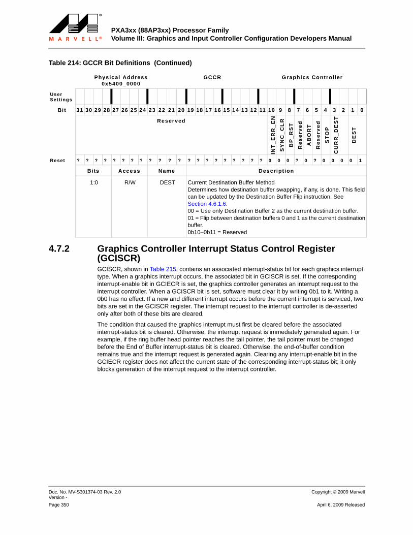
PXA3xx (88AP3xx) Processor FamilyVolume III: Graphics and Input Controller Configuration Developers Manual
Doc. No. MV-S301374-03 Rev. 2.0 Version -
Copyright © 2009 Marvell
Page 350 April 6, 2009 Released
12345678910111213141516171819202122232425262728293031323334353637383940414243444546474849505152535455565758
4.7.2 Graphics Controller Interrupt Status Control Register (GCISCR)GCISCR, shown in Table 215, contains an associated interrupt-status bit for each graphics interrupt type. When a graphics interrupt occurs, the associated bit in GCISCR is set. If the corresponding interrupt-enable bit in GCIECR is set, the graphics controller generates an interrupt request to the interrupt controller. When a GCISCR bit is set, software must clear it by writing 0b1 to it. Writing a 0b0 has no effect. If a new and different interrupt occurs before the current interrupt is serviced, two bits are set in the GCISCR register. The interrupt request to the interrupt controller is de-asserted only after both of these bits are cleared.
The condition that caused the graphics interrupt must first be cleared before the associated interrupt-status bit is cleared. Otherwise, the interrupt request is immediately generated again. For example, if the ring buffer head pointer reaches the tail pointer, the tail pointer must be changed before the End of Buffer interrupt-status bit is cleared. Otherwise, the end-of-buffer condition remains true and the interrupt request is generated again. Clearing any interrupt-enable bit in the GCIECR register does not affect the current state of the corresponding interrupt-status bit; it only blocks generation of the interrupt request to the interrupt controller.
1:0 R/W DEST Current Destination Buffer MethodDetermines how destination buffer swapping, if any, is done. This field can be updated by the Destination Buffer Flip instruction. See Section 4.6.1.6.00 = Use only Destination Buffer 2 as the current destination buffer.01 = Flip between destination buffers 0 and 1 as the current destination buffer.0b10–0b11 = Reserved
Table 214: GCCR Bit Definitions (Continued)
Physical Address0x5400_0000
GCCR Graphics Controller
User Settings
Bit 31 30 29 28 27 26 25 24 23 22 21 20 19 18 17 16 15 14 13 12 11 10 9 8 7 6 5 4 3 2 1 0
Reserved
INT
_E
RR
_E
N
SY
NC
_C
LR
BP
_R
ST
Re
se
rve
d
AB
OR
T
Re
se
rve
d
ST
OP
CU
RR
_D
ES
T
DE
ST
Reset ? ? ? ? ? ? ? ? ? ? ? ? ? ? ? ? ? ? ? ? ? 0 0 0 ? 0 ? 0 0 0 0 1
Bits Access Name Descript ion

Graphics ControllerRegister Descriptions
Copyright © 2009 Marvell Doc. No. MV-S301374-03 Rev. 2.0Version -
April 6, 2009 Released Page 351
12345678910111213141516171819202122232425262728293031323334353637383940414243444546474849505152535455565758
Table 215: GCISCR Bit Definitions
Physical Address0x5400_0004
GCISCR Graphics Control ler
User Settings
Bit 31 30 29 28 27 26 25 24 23 22 21 20 19 18 17 16 15 14 13 12 11 10 9 8 7 6 5 4 3 2 1 0
IN_INT_ID
Re
se
rve
d
ST
OP
_IN
TS
T
PF
_IN
TS
T
EE
OB
_IN
TS
T
IIN
_IN
TS
T
IOP
_IN
TS
T
BF
_IN
TS
T
IN_
INT
ST
EO
B_
INT
ST
Reset 0 0 0 0 0 0 0 0 0 0 0 0 0 0 0 0 0 0 0 0 ? ? ? ? 0 0 0 0 0 0 0 0
Bits Access Name Description
31:12 R/W IN_INT_ID Interrupt IdentificationInterrupt ID to the core for an instruction interrupt, which is generated by the GC_INT graphics controller Instruction. See Section 4.6.1.8. If you want to preserve the value in this field when clearing other GCISCR status bits, the contents of the GCISCR register should be read so that the field value can be determined, and then it should be written back. Because this field is read/write, any value programmed here is written to this field.
11:9 — — Reserved
8 — — Reserved
7 R/W 1 to clear
STOP_INTST Stop Interrupt StatusGCCR[STOP] Response interrupt status. 0 = The graphics controller has not stopped all activity due to a
GCCR[STOP] assertion.1 = The graphics controller has stopped all activity due to a
GCCR[STOP] assertion.
6 R/W 1 to clear
PF_INTST Pixel Format Interrupt StatusIllegal pixel format, illegal step size, or incompatible pixel format and step size interrupt status. This interrupt condition is checked only when the Ring Buffer Length register is programmed to a value other than all zeros.0 = No illegal/incompatible pixel format or step size.1 = An illegal/incompatible pixel format or step size.
5 R/W 1 to clear
EEOB_INTST Execution End of Buffer Interrupt StatusFor this interrupt, the ring buffer execution HEAD = ring buffer tail. If the last instruction in the ring buffer is a batch buffer start, execution within the batch buffer can occur even when this execution End of Buffer interrupt is received.0 = No Execution End of Buffer.1 = An Execution End of Buffer.
4 R/W 1 to clear
IIN_INTST Illegal Instruction Interrupt StatusIn an illegal instruction, the GCI type field of the first word is neither memory nor 2-D graphics.0 = No Illegal instruction.1 = An Illegal instruction.

PXA3xx (88AP3xx) Processor FamilyVolume III: Graphics and Input Controller Configuration Developers Manual
Doc. No. MV-S301374-03 Rev. 2.0 Version -
Copyright © 2009 Marvell
Page 352 April 6, 2009 Released
12345678910111213141516171819202122232425262728293031323334353637383940414243444546474849505152535455565758
4.7.3 Graphics Controller Interrupt Enable Control Register (GCIECR)GCIECR, shown in Table 216, contains an associated an interrupt-enable bit for each graphics interrupt. When an interrupt condition occurs, the associated bit in GCISCR is set, and if the corresponding interrupt-enable bit in GCIECR is also set, the graphics interrupt request is generated and sent to the interrupt controller. This is a read/write register. Ignore reads from reserved bits. Write 0b0 to reserved bits. Clearing any interrupt-enable bit does not affect the current state of the corresponding interrupt-status bit in the Interrupt Status Control Register; it only blocks assertion of the graphics controller interrupt.
3 R/W 1 to clear
IOP_INTST Illegal Operation Interrupt StatusIn an illegal operation, the Opcode field of the first word of an instruction is not in the valid instruction set of the GCI Type.0 = No Illegal operation.1 = An Illegal operation.
2 R/W 1 to clear
BF_INTST Display Buffer Flip Interrupt Status 0 = No Display Buffer Flip Instruction has executed.1 = A Display Buffer Flip Instruction has executed
1 R/W 1 to clear
IN_INTST Instruction Interrupt Status. This bit is set by the GC_INT graphics controller Instruction. See Section 4.6.1.8. 0 = No instruction interrupt.1 = An instruction interrupt.
0 R/W 1 to clear
EOB_INTST End of Buffer Interrupt StatusEnd of Buffer (Ring buffer HEAD = ring buffer TAIL) interrupt status. 0 = No End of Buffer.1 = An End of Buffer.
Table 215: GCISCR Bit Definitions (Continued)
Physical Address0x5400_0004
GCISCR Graphics Control ler
User Settings
Bit 31 30 29 28 27 26 25 24 23 22 21 20 19 18 17 16 15 14 13 12 11 10 9 8 7 6 5 4 3 2 1 0
IN_INT_ID
Re
se
rve
d
ST
OP
_IN
TS
T
PF
_IN
TS
T
EE
OB
_IN
TS
T
IIN
_IN
TS
T
IOP
_IN
TS
T
BF
_IN
TS
T
IN_
INT
ST
EO
B_
INT
ST
Reset 0 0 0 0 0 0 0 0 0 0 0 0 0 0 0 0 0 0 0 0 ? ? ? ? 0 0 0 0 0 0 0 0
Bits Access Name Description
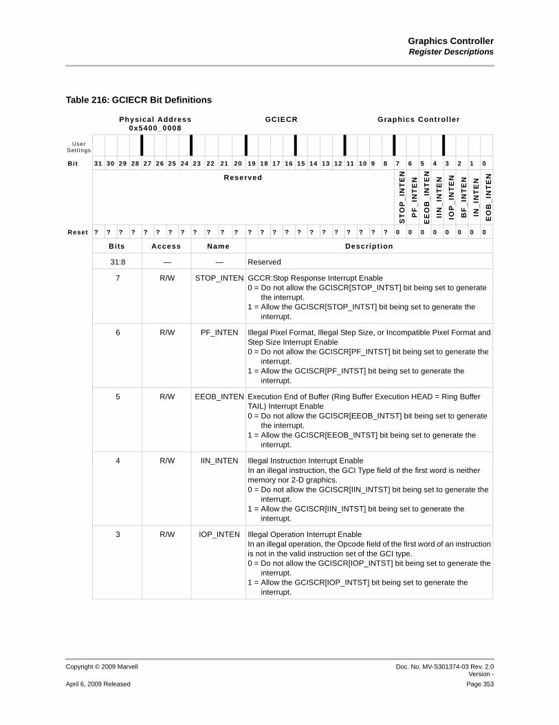
Graphics ControllerRegister Descriptions
Copyright © 2009 Marvell Doc. No. MV-S301374-03 Rev. 2.0Version -
April 6, 2009 Released Page 353
12345678910111213141516171819202122232425262728293031323334353637383940414243444546474849505152535455565758
Table 216: GCIECR Bit Definitions
Physical Address0x5400_0008
GCIECR Graphics Controller
User Sett ings
Bit 31 30 29 28 27 26 25 24 23 22 21 20 19 18 17 16 15 14 13 12 11 10 9 8 7 6 5 4 3 2 1 0
Reserved
ST
OP
_IN
TE
N
PF
_IN
TE
N
EE
OB
_IN
TE
N
IIN
_IN
TE
N
IOP
_IN
TE
N
BF
_IN
TE
N
IN_
INT
EN
EO
B_
INT
EN
Reset ? ? ? ? ? ? ? ? ? ? ? ? ? ? ? ? ? ? ? ? ? ? ? ? 0 0 0 0 0 0 0 0
Bits Access Name Descript ion
31:8 — — Reserved
7 R/W STOP_INTEN GCCR:Stop Response Interrupt Enable0 = Do not allow the GCISCR[STOP_INTST] bit being set to generate
the interrupt.1 = Allow the GCISCR[STOP_INTST] bit being set to generate the
interrupt.
6 R/W PF_INTEN Illegal Pixel Format, Illegal Step Size, or Incompatible Pixel Format and Step Size Interrupt Enable0 = Do not allow the GCISCR[PF_INTST] bit being set to generate the
interrupt.1 = Allow the GCISCR[PF_INTST] bit being set to generate the
interrupt.
5 R/W EEOB_INTEN Execution End of Buffer (Ring Buffer Execution HEAD = Ring Buffer TAIL) Interrupt Enable0 = Do not allow the GCISCR[EEOB_INTST] bit being set to generate
the interrupt.1 = Allow the GCISCR[EEOB_INTST] bit being set to generate the
interrupt.
4 R/W IIN_INTEN Illegal Instruction Interrupt EnableIn an illegal instruction, the GCI Type field of the first word is neither memory nor 2-D graphics.0 = Do not allow the GCISCR[IIN_INTST] bit being set to generate the
interrupt.1 = Allow the GCISCR[IIN_INTST] bit being set to generate the
interrupt.
3 R/W IOP_INTEN Illegal Operation Interrupt EnableIn an illegal operation, the Opcode field of the first word of an instruction is not in the valid instruction set of the GCI type.0 = Do not allow the GCISCR[IOP_INTST] bit being set to generate the
interrupt.1 = Allow the GCISCR[IOP_INTST] bit being set to generate the
interrupt.

PXA3xx (88AP3xx) Processor FamilyVolume III: Graphics and Input Controller Configuration Developers Manual
Doc. No. MV-S301374-03 Rev. 2.0 Version -
Copyright © 2009 Marvell
Page 354 April 6, 2009 Released
12345678910111213141516171819202122232425262728293031323334353637383940414243444546474849505152535455565758
4.7.4 Graphics Controller NOP ID Register (GCNOPID)GCNOPID, shown in Table 217, contains an associated NOP ID value for each NOP instruction encountered in the graphics instruction stream. This 20-bit NOP ID value is automatically written into the GCNOPID register.
2 R/W BF_INTEN Buffer Flip Interrupt Enable0 = Do not allow the GCISCR[BF_INTST] bit being set to generate the
interrupt.1 = Allow the GCISCR[BF_INTST] bit being set to generate the
interrupt.
1 R/W IN_INTEN Instruction Interrupt Enable0 = Do not allow the GCISCR[IN_INTST] bit being set to generate the
interrupt.1 = Allow the GCISCR[IN_INTST] bit being set to generate the interrupt.
0 R/W EOB_INTEN End of Buffer (Ring Buffer HEAD = Ring Buffer TAIL) Interrupt Enable0 = Do not allow the GCISCR[EOB_INTST] bit being set to generate the
interrupt.1 = Allow the GCISCR[EOB_INTST] bit being set to generate the
interrupt.
Table 216: GCIECR Bit Definitions (Continued)
Physical Address0x5400_0008
GCIECR Graphics Controller
User Sett ings
Bit 31 30 29 28 27 26 25 24 23 22 21 20 19 18 17 16 15 14 13 12 11 10 9 8 7 6 5 4 3 2 1 0
Reserved
ST
OP
_IN
TE
N
PF
_IN
TE
N
EE
OB
_IN
TE
N
IIN
_IN
TE
N
IOP
_IN
TE
N
BF
_IN
TE
N
IN_
INT
EN
EO
B_
INT
EN
Reset ? ? ? ? ? ? ? ? ? ? ? ? ? ? ? ? ? ? ? ? ? ? ? ? 0 0 0 0 0 0 0 0
Bits Access Name Descript ion
Table 217: GCNOPID Bit Definitions
Physical Address0x5400_000C
GCNOPID Graphics Controller
User Sett ings
Bit 31 30 29 28 27 26 25 24 23 22 21 20 19 18 17 16 15 14 13 12 11 10 9 8 7 6 5 4 3 2 1 0
Reserved NOP_ID
Reset ? ? ? ? ? ? ? ? ? ? ? ? 0 0 0 0 0 0 0 0 0 0 0 0 0 0 0 0 0 0 0 0
Bits Access Name Descript ion
31:20 — — Reserved

Graphics ControllerRegister Descriptions
Copyright © 2009 Marvell Doc. No. MV-S301374-03 Rev. 2.0Version -
April 6, 2009 Released Page 355
12345678910111213141516171819202122232425262728293031323334353637383940414243444546474849505152535455565758
4.7.5 Graphics Controller Default Alpha Setting Register (GCALPHASET)GCALPHASET, shown in Table 218, contains the written alpha value for conversions of the RGB or RGBT in/out formats to the internal RGBA format. During the conversion process, an alpha value is created. The desired alpha value for such conversions is written into the register.
19:0 R/W NOP_ID NOP Identification valueThe GC_NOP instruction has a NOP ID field. When a GC_NOP instruction is fetched from the graphics instruction stream, its NOP ID field is automatically written to GCNOPID_[NOP_ID]. See Section 4.6.1.5. Some NOP IDs define special functions and are written by the graphics controller or by software:0xFFFFF = Set the internal crash stop signal (written by software).0xFFFFE = Set the internal breakpoint out signal (written by software).0xFFFFD = Target abort on System Bus 2 (written by the graphics controller).0xFFFFC = Master abort on System Bus 2 (written by the graphics controller).0xFFFFB = Internal error in the graphics controller and GCCR_[INT_ERR_EN] is set (written by the graphics controller).0xFFFFA= Internal error in the graphics controller and GCCR_[INT_ERR_EN] is cleared (written by the graphics controller).
Table 217: GCNOPID Bit Definitions (Continued)
Physical Address0x5400_000C
GCNOPID Graphics Controller
User Sett ings
Bit 31 30 29 28 27 26 25 24 23 22 21 20 19 18 17 16 15 14 13 12 11 10 9 8 7 6 5 4 3 2 1 0
Reserved NOP_ID
Reset ? ? ? ? ? ? ? ? ? ? ? ? 0 0 0 0 0 0 0 0 0 0 0 0 0 0 0 0 0 0 0 0
Bits Access Name Descript ion
Table 218: GCALPHASET Bit Definitions
Physical Address0x5400_0010
GCALPHASET Graphics Control ler
User Sett ings
Bit 31 30 29 28 27 26 25 24 23 22 21 20 19 18 17 16 15 14 13 12 11 10 9 8 7 6 5 4 3 2 1 0
Reserved
VA
LID ALPHA
Reset ? ? ? ? ? ? ? ? ? ? ? ? ? ? ? 1 0 0 0 0 0 0 0 0 0 0 0 0 0 0 0 0
Bits Access Name Descript ion
31:17 — — Reserved

PXA3xx (88AP3xx) Processor FamilyVolume III: Graphics and Input Controller Configuration Developers Manual
Doc. No. MV-S301374-03 Rev. 2.0 Version -
Copyright © 2009 Marvell
Page 356 April 6, 2009 Released
12345678910111213141516171819202122232425262728293031323334353637383940414243444546474849505152535455565758
4.7.6 Graphics Controller Default Transparency Setting Register (GCTSET)GCTSET, shown in Table 219, selects the source of the desired transparency value for conversions the graphics controller internal RGBA format to the RGBT output format. During the conversion process a transparency value is created.
16 R/W VALID Valid alpha value selection0 = Do not use the default ALPHA value in GCALPHASET_[ALPHA]
when converting to RGBA pixel format. Instead, when converting from RGB format, use all 0b0s instead of the ALPHA field. When converting from RGBT format, use the definition in Table 149.
1 = Use the default ALPHA value in GCALPHASET_[ALPHA] when converting to RGBA format.
15:0 R/W ALPHA 16-bit default ALPHA value for use according to GCALPHASET_[VALID].
Table 218: GCALPHASET Bit Definitions (Continued)
Physical Address0x5400_0010
GCALPHASET Graphics Control ler
User Sett ings
Bit 31 30 29 28 27 26 25 24 23 22 21 20 19 18 17 16 15 14 13 12 11 10 9 8 7 6 5 4 3 2 1 0
Reserved
VA
LID ALPHA
Reset ? ? ? ? ? ? ? ? ? ? ? ? ? ? ? 1 0 0 0 0 0 0 0 0 0 0 0 0 0 0 0 0
Bits Access Name Descript ion
Table 219: GCTSET Bit Definitions
Physical Address0x5400_0014
GCTSET Graphics Controller
User Sett ings
Bit 31 30 29 28 27 26 25 24 23 22 21 20 19 18 17 16 15 14 13 12 11 10 9 8 7 6 5 4 3 2 1 0
Reserved
VA
LID Reserved
TB
IT
Reset ? ? ? ? ? ? ? ? ? ? ? ? ? ? ? 1 ? ? ? ? ? ? ? ? ? ? ? ? ? ? ? 0
Bits Access Name Descript ion
31:17 — — Reserved
16 R/W VALID Valid transparency value selection0 = Do not use the default transparency value programmed in
GCTSET_[TBIT] when converting to RGBT pixel format. Instead, when converting from RGBA format, use the transparency value defined in Table 149.
1 = Use the default transparency value in GCTSET_[TBIT] when converting to RGBT format.
15:1 — — Reserved
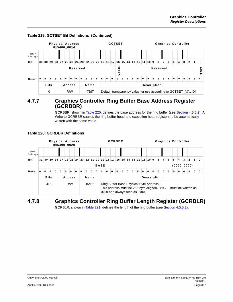
Graphics ControllerRegister Descriptions
Copyright © 2009 Marvell Doc. No. MV-S301374-03 Rev. 2.0Version -
April 6, 2009 Released Page 357
12345678910111213141516171819202122232425262728293031323334353637383940414243444546474849505152535455565758
4.7.7 Graphics Controller Ring Buffer Base Address Register (GCRBBR)GCRBBR, shown in Table 220, defines the base address for the ring buffer (see Section 4.5.5.2). A Write to GCRBBR causes the ring buffer head and execution head registers to be automatically written with the same value.
4.7.8 Graphics Controller Ring Buffer Length Register (GCRBLR)GCRBLR, shown in Table 221, defines the length of the ring buffer (see Section 4.5.5.2).
0 R/W TBIT Default transparency value for use according to GCTSET_[VALID].
Table 219: GCTSET Bit Definitions (Continued)
Physical Address0x5400_0014
GCTSET Graphics Controller
User Sett ings
Bit 31 30 29 28 27 26 25 24 23 22 21 20 19 18 17 16 15 14 13 12 11 10 9 8 7 6 5 4 3 2 1 0
Reserved
VA
LID Reserved
TB
IT
Reset ? ? ? ? ? ? ? ? ? ? ? ? ? ? ? 1 ? ? ? ? ? ? ? ? ? ? ? ? ? ? ? 0
Bits Access Name Descript ion
Table 220: GCRBBR Definitions
Physical Address0x5400_0020
GCRBBR Graphics Controller
User Sett ings
Bit 31 30 29 28 27 26 25 24 23 22 21 20 19 18 17 16 15 14 13 12 11 10 9 8 7 6 5 4 3 2 1 0
BASE (0000_0000)
Reset 0 0 0 0 0 0 0 0 0 0 0 0 0 0 0 0 0 0 0 0 0 0 0 0 0 0 0 0 0 0 0 0
Bits Access Name Descript ion
31:0 R/W BASE Ring Buffer Base Physical Byte AddressThis address must be 256-byte aligned. Bits 7:0 must be written as 0x00 and always read as 0x00.

PXA3xx (88AP3xx) Processor FamilyVolume III: Graphics and Input Controller Configuration Developers Manual
Doc. No. MV-S301374-03 Rev. 2.0 Version -
Copyright © 2009 Marvell
Page 358 April 6, 2009 Released
12345678910111213141516171819202122232425262728293031323334353637383940414243444546474849505152535455565758
4.7.9 Graphics Controller Ring Buffer Head Register (GCRBHR)GCRBHR, shown in Table 222, defines the head pointer to the ring buffer. The graphics controller maintains this physical address, and software cannot write to it. A Write to the Ring Buffer Base Address (GCRBBR) register causes the Ring Buffer Head Register to be written with this same value. Software should monitor the GCRBHR register to check ring buffer memory accesses. register defines the point in memory from which the graphics controller actually fetches an instruction from the ring buffer. When the head pointer reaches the tail pointer (in the GCRBTR register), the GCISCR[EOB_INTST] bit is set and an interrupt request is generated.
4.7.10 Graphics Controller Ring Buffer Tail Register (GCRBTR)GCRBTR, shown in Table 223, defines the tail pointer to the ring buffer.
Table 221: GCRBLR Bit Definitions
Physical Address0x5400_0024
GCRBLR Graphics Controller
User Sett ings
Bit 31 30 29 28 27 26 25 24 23 22 21 20 19 18 17 16 15 14 13 12 11 10 9 8 7 6 5 4 3 2 1 0
Reserved LENGTH (0000_0000)
Reset ? ? ? ? ? ? ? ? ? ? ? ? ? ? 0 0 0 0 0 0 0 0 0 0 0 0 0 0 0 0 0 0
Bits Access Name Descript ion
31:18 — — Reserved
17:0 R/W LENGTH Ring Buffer LengthThe ring buffer can be 256 Kbytes – 256 bytes long and must be 256-byte aligned. This address must be 256-byte aligned. Bits 7:0 must be written as 0x00 and always read as 0x00.
Table 222: GCRBHR Bit Definitions
Physical Address0x5400_0028
GCRBHR Graphics Controller
User Sett ings
Bit 31 30 29 28 27 26 25 24 23 22 21 20 19 18 17 16 15 14 13 12 11 10 9 8 7 6 5 4 3 2 1 0
HEAD (00)
Reset 0 0 0 0 0 0 0 0 0 0 0 0 0 0 0 0 0 0 0 0 0 0 0 0 0 0 0 0 0 0 0 0
Bits Access Name Descript ion
31:0 R HEAD Ring Buffer Head Physical Byte AddressThis address is 4-byte aligned. Bits 1:0 always read as 0b00.

Graphics ControllerRegister Descriptions
Copyright © 2009 Marvell Doc. No. MV-S301374-03 Rev. 2.0Version -
April 6, 2009 Released Page 359
12345678910111213141516171819202122232425262728293031323334353637383940414243444546474849505152535455565758
4.7.11 Graphics Controller Ring Buffer Execution Head Register (GCRBEXHR)GCRBEXHR, shown in Table 224, defines the execution head pointer to the ring buffer. The graphics controller maintains this physical address, and software cannot directly write to it. A Write to the Ring Buffer Base Address (GCRBBR) register causes GCRBEXHR to be written with this same value. Software should monitor GCRBEXHR to check which instruction from the ring buffer is executing. GCRBEXHR points to the next instruction in the ring buffer to be executed (or is being executed). When an instruction finishes executing, the execution head pointer is automatically incremented by the number of words in the executed instruction. It always points to the first word of an instruction. For example, if the next instruction to execute is 5 words long, the pointer always points to word 0. When the execution head pointer reaches the tail pointer (in the GCRBTR register), the GCISCR[EEOB_INTST] bit is automatically set and a graphics interrupt request is generated. If the last instruction in the ring buffer is a Batch Buffer Start instruction, execution within the batch buffer can still occur even though the GCISCR[EEOB_INTST] bit is set.
4.7.12 Graphics Controller Batch Buffer Base Address Register (GCBBBR)GCBBBR, shown in Table 225, defines the base address for a batch buffer (see Section 4.5.5.3). A Batch Buffer Start instruction causes the Batch Buffer Base (GCBBBR) register, Batch Buffer Head
Table 223: GCRBTR Bit Definitions
Physical Address0x5400_002C
GCRBTR Graphics Controller
User Sett ings
Bit 31 30 29 28 27 26 25 24 23 22 21 20 19 18 17 16 15 14 13 12 11 10 9 8 7 6 5 4 3 2 1 0
TAIL (00)
Reset 0 0 0 0 0 0 0 0 0 0 0 0 0 0 0 0 0 0 0 0 0 0 0 0 0 0 0 0 0 0 0 0
Bits Access Name Descript ion
31:0 R/W TAIL Ring Buffer Tail Physical Byte Address his address must be 4-byte aligned. Bits 1:0 must be written as 0b00 and always read as 0b00.
Table 224: GCRBEXHR Bit Definitions
Physical Address0x5400_0030
GCRBEXHR Graphics Controller
User Sett ings
Bit 31 30 29 28 27 26 25 24 23 22 21 20 19 18 17 16 15 14 13 12 11 10 9 8 7 6 5 4 3 2 1 0
EX_HEAD (00)
Reset 0 0 0 0 0 0 0 0 0 0 0 0 0 0 0 0 0 0 0 0 0 0 0 0 0 0 0 0 0 0 0 0
Bits Access Name Descript ion
31:0 R EX_HEAD Ring Buffer Execution Head Physical Byte Address This address is 4-byte aligned. Bits 1:0 always read as 0b00.

PXA3xx (88AP3xx) Processor FamilyVolume III: Graphics and Input Controller Configuration Developers Manual
Doc. No. MV-S301374-03 Rev. 2.0 Version -
Copyright © 2009 Marvell
Page 360 April 6, 2009 Released
12345678910111213141516171819202122232425262728293031323334353637383940414243444546474849505152535455565758
(GCBBHR) register, and Batch Buffer Execution Head (GCBBEXHR) register to be written with the address specified in the instruction. The GCBBBR register is read-only.
4.7.13 Graphics Controller Batch Buffer Head Register (GCBBHR)GCBBHR, shown in Table 226, defines the head pointer to the batch buffer. The graphics controller maintains this physical address, and software cannot write to it. A Batch Buffer Start instruction causes GCBBHR to be written with the address specified in the instruction. Software should monitor the GCBBHR register to check batch buffer memory accesses. GCBBHR defines the memory location in the batch buffer at which the graphics controller actually fetches the instruction. The batch buffer head register is always incremented by 8 words after each Read because each Read is 8 words long. The head register points to the next Read address. After all the instructions are read from a batch buffer that ends with the GC_BBEND instruction, the GCBBHR value is irrelevant because there are no more Reads from the batch buffer.
4.7.14 Graphics Controller Batch Buffer Execution Head Register (GCBBEXHR)GCBBEXHR, shown in Table 227, defines the execution head pointer to the batch buffer. The graphics controller maintains this physical address, and software cannot write to it. A Batch Buffer Start instruction causes GCBBEXHR to be written with the address specified in the instruction. Software must monitor the GCBBEXHR register to check batch buffer execution. GCBBEXHR points to the next location in the batch buffer to execute (or being executed). Once an instruction finishes executing, the execution head pointer is automatically incremented by the number of words in the
Table 225: GCBBBR Bit Definitions
Physical Address0x5400_0040
GCBBBR Graphics Controller
User Sett ings
Bit 31 30 29 28 27 26 25 24 23 22 21 20 19 18 17 16 15 14 13 12 11 10 9 8 7 6 5 4 3 2 1 0
BASE (00)
Reset 0 0 0 0 0 0 0 0 0 0 0 0 0 0 0 0 0 0 0 0 0 0 0 0 0 0 0 0 0 0 0 0
Bits Access Name Descript ion
31:0 R BASE Batch Buffer Base Physical Byte AddressThis address is 4-byte aligned. Bits 1:0 always read as 0b00.
Table 226: GCBBHR Bit Definitions
Physical Address0x5400_0044
GCBBHR Graphics Controller
User Sett ings
Bit 31 30 29 28 27 26 25 24 23 22 21 20 19 18 17 16 15 14 13 12 11 10 9 8 7 6 5 4 3 2 1 0
HEAD (00)
Reset 0 0 0 0 0 0 0 0 0 0 0 0 0 0 0 0 0 0 0 0 0 0 0 0 0 0 0 0 0 0 0 0
Bits Access Name Descript ion
31:0 R HEAD Batch Buffer Head Physical Byte AddressThis address is 4-byte aligned. Bits 1:0 always read as 0b00.

Graphics ControllerRegister Descriptions
Copyright © 2009 Marvell Doc. No. MV-S301374-03 Rev. 2.0Version -
April 6, 2009 Released Page 361
12345678910111213141516171819202122232425262728293031323334353637383940414243444546474849505152535455565758
executed instruction. It always points to the first word of an instruction. For example, if the next instruction to execute is 5 words long, the execution head always points to word 0.
4.7.15 Graphics Controller Destination Buffer 0 (Display Buffer 0) Base Address Register (GCD0BR)GCD0BR, shown in Table 228, defines the base address for Destination Buffer 0 (Display Buffer 0).
4.7.16 Graphics Controller Destination Buffer 0 (Display Buffer 0) Step Size Register (GCD0STP)GCD0STP, shown in Table 229, defines the step size for Destination Buffer 0 (Display Buffer 0). Step size is the number of bytes used to define one pixel.
Table 227: GCBBEXHR Bit Definitions
Physical Address0x5400_0048
GCBBEXHR Graphics Controller
User Sett ings
0 0
Bit 31 30 29 28 27 26 25 24 23 22 21 20 19 18 17 16 15 14 13 12 11 10 9 8 7 6 5 4 3 2 1 0
EX_HEAD (00)
Reset 0 0 0 0 0 0 0 0 0 0 0 0 0 0 0 0 0 0 0 0 0 0 0 0 0 0 0 0 0 0 0 0
Bits Access Name Descript ion
31:0 R EX_HEAD Batch Buffer Execution HEAD Physical Byte Address This address is 4-byte aligned. Bits 1:0 always read as 0b00.
Table 228: GCD0BR Bit Definitions
Physical Address0x5400_0060
GCD0BR Graphics Controller
User Sett ings
0 0 0
Bit 31 30 29 28 27 26 25 24 23 22 21 20 19 18 17 16 15 14 13 12 11 10 9 8 7 6 5 4 3 2 1 0
BASE (000)
Reset 0 0 0 0 0 0 0 0 0 0 0 0 0 0 0 0 0 0 0 0 0 0 0 0 0 0 0 0 0 0 0 0
Bits Access Name Descript ion
31:0 R/W BASE Destination Buffer 0 (Also the Display Buffer 0) Base Physical Byte AddressThis address must be 8-byte aligned. Bits 2:0 must be written as 0b000 and always read as 0b000.

PXA3xx (88AP3xx) Processor FamilyVolume III: Graphics and Input Controller Configuration Developers Manual
Doc. No. MV-S301374-03 Rev. 2.0 Version -
Copyright © 2009 Marvell
Page 362 April 6, 2009 Released
12345678910111213141516171819202122232425262728293031323334353637383940414243444546474849505152535455565758
4.7.17 Graphics Controller Destination Buffer 0 (Display Buffer 0) Stride Size Register (GCD0STR)GCD0STR, shown in Table 230, defines the stride size for Destination Buffer 0 (Display Buffer 0). Stride size is the number of bytes that the total number of pixels in a line occupy.
4.7.18 Graphics Controller Destination Buffer 0 (Display Buffer 0) Pixel Format Register (GCD0PF)GCD0PF, shown in Table 231, defines the pixel format for Destination Buffer 0 (Display Buffer 0). The pixel format can differ for each of the three destination buffers. The format selected for Destination Buffer 0 must be the same as that selected for the LCD controller Display Buffer 0.
Table 229: GCD0STP Bit Definitions
Physical Address0x5400_0064
GCD0STP Graphics Controller
User Sett ings
Bit 31 30 29 28 27 26 25 24 23 22 21 20 19 18 17 16 15 14 13 12 11 10 9 8 7 6 5 4 3 2 1 0
Reserved STEP
Reset ? ? ? ? ? ? ? ? ? ? ? ? ? ? ? ? ? ? ? ? ? ? ? ? ? ? ? ? 1 0 0 0
Bits Access Name Descript ion
31:4 — — Reserved
3:0 R/W STEP Destination Buffer 0 (Display Buffer 0) Step Size in BytesValid options are shown. All other options are invalid and are set based on the pixel format.0b0001 = 1 byte per pixel0b0010 = 2 bytes per pixel0b0011 = 3 bytes per pixel0b0100 = 4 bytes per pixel0b1000 = 8 bytes per pixel
Table 230: GCD0STR Bit Definitions
Physical Address0x5400_0068
GCD0STR Graphics Controller
User Sett ings
Bit 31 30 29 28 27 26 25 24 23 22 21 20 19 18 17 16 15 14 13 12 11 10 9 8 7 6 5 4 3 2 1 0
Reserved STRIDE
Reset ? ? ? ? ? ? ? ? ? ? ? ? ? ? ? ? ? ? 0 0 0 0 0 0 0 0 0 0 0 0 0 0
Bits Access Name Descript ion
31:14 — — Reserved
13:0 R/W STRIDE Destination Buffer 0 (Display Buffer 0) Stride Size in BytesThis number supports up to 16383 bytes per line where STRIDE value = x-bytes per pixel times y-pixels per line.

Graphics ControllerRegister Descriptions
Copyright © 2009 Marvell Doc. No. MV-S301374-03 Rev. 2.0Version -
April 6, 2009 Released Page 363
12345678910111213141516171819202122232425262728293031323334353637383940414243444546474849505152535455565758
4.7.19 Graphics Controller Destination Buffer 1 (Display Buffer 1) Base Address Register (GCD1BR)GCD1BR, shown in Table 232, defines the base address for Destination Buffer 1 (Display Buffer 1).
4.7.20 Graphics Controller Destination Buffer 1 (Display Buffer 1) Step Size Register (GCD1STP)GCD1STP, shown in Table 233, defines the step size for Destination Buffer 1 (Display Buffer 1). Step size is the number of bytes used to define one pixel.
Table 231: GCD0PF Bit Definitions
Physical Address0x5400_006C
GCD0PF Graphics Controller
User Sett ings
Bit 31 30 29 28 27 26 25 24 23 22 21 20 19 18 17 16 15 14 13 12 11 10 9 8 7 6 5 4 3 2 1 0
Reserved PFORM
Reset ? ? ? ? ? ? ? ? ? ? ? ? ? ? ? ? ? ? ? ? ? ? ? ? ? ? ? ? 1 0 1 1
Bits Access Name Descript ion
31:4 — — Reserved
3:0 R/W PFORM The pixel format for Destination Buffer 0 (Display Buffer 0). See Section 4.5.7
Table 232: GCD1BR Bit Definitions
Physical Address0x5400_0070
GCD1BR Graphics Controller
User Sett ings
0 0 0
Bit 31 30 29 28 27 26 25 24 23 22 21 20 19 18 17 16 15 14 13 12 11 10 9 8 7 6 5 4 3 2 1 0
BASE (000)
Reset 0 0 0 0 0 0 0 0 0 0 0 0 0 0 0 0 0 0 0 0 0 0 0 0 0 0 0 0 0 0 0 0
Bits Access Name Descript ion
31:0 R/W BASE Destination Buffer 1 (Also the Display Buffer 1) Base Physical Byte AddressThis address must be 8-byte aligned. Bits 2:0 must be written as 0b000 and always read as 0b000.
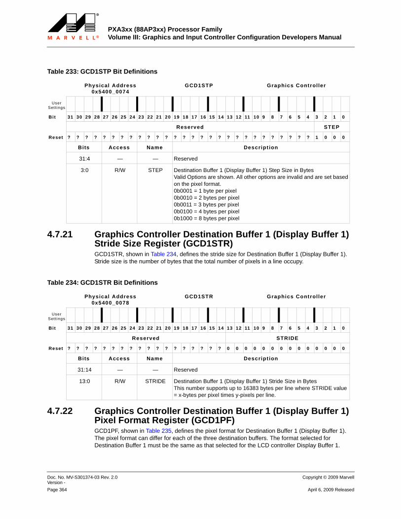
PXA3xx (88AP3xx) Processor FamilyVolume III: Graphics and Input Controller Configuration Developers Manual
Doc. No. MV-S301374-03 Rev. 2.0 Version -
Copyright © 2009 Marvell
Page 364 April 6, 2009 Released
12345678910111213141516171819202122232425262728293031323334353637383940414243444546474849505152535455565758
4.7.21 Graphics Controller Destination Buffer 1 (Display Buffer 1) Stride Size Register (GCD1STR)GCD1STR, shown in Table 234, defines the stride size for Destination Buffer 1 (Display Buffer 1). Stride size is the number of bytes that the total number of pixels in a line occupy.
4.7.22 Graphics Controller Destination Buffer 1 (Display Buffer 1) Pixel Format Register (GCD1PF)GCD1PF, shown in Table 235, defines the pixel format for Destination Buffer 1 (Display Buffer 1). The pixel format can differ for each of the three destination buffers. The format selected for Destination Buffer 1 must be the same as that selected for the LCD controller Display Buffer 1.
Table 233: GCD1STP Bit Definitions
Physical Address0x5400_0074
GCD1STP Graphics Controller
User Sett ings
Bit 31 30 29 28 27 26 25 24 23 22 21 20 19 18 17 16 15 14 13 12 11 10 9 8 7 6 5 4 3 2 1 0
Reserved STEP
Reset ? ? ? ? ? ? ? ? ? ? ? ? ? ? ? ? ? ? ? ? ? ? ? ? ? ? ? ? 1 0 0 0
Bits Access Name Descript ion
31:4 — — Reserved
3:0 R/W STEP Destination Buffer 1 (Display Buffer 1) Step Size in BytesValid Options are shown. All other options are invalid and are set based on the pixel format.0b0001 = 1 byte per pixel0b0010 = 2 bytes per pixel0b0011 = 3 bytes per pixel0b0100 = 4 bytes per pixel0b1000 = 8 bytes per pixel
Table 234: GCD1STR Bit Definitions
Physical Address0x5400_0078
GCD1STR Graphics Controller
User Sett ings
Bit 31 30 29 28 27 26 25 24 23 22 21 20 19 18 17 16 15 14 13 12 11 10 9 8 7 6 5 4 3 2 1 0
Reserved STRIDE
Reset ? ? ? ? ? ? ? ? ? ? ? ? ? ? ? ? ? ? 0 0 0 0 0 0 0 0 0 0 0 0 0 0
Bits Access Name Descript ion
31:14 — — Reserved
13:0 R/W STRIDE Destination Buffer 1 (Display Buffer 1) Stride Size in BytesThis number supports up to 16383 bytes per line where STRIDE value = x-bytes per pixel times y-pixels per line.

Graphics ControllerRegister Descriptions
Copyright © 2009 Marvell Doc. No. MV-S301374-03 Rev. 2.0Version -
April 6, 2009 Released Page 365
12345678910111213141516171819202122232425262728293031323334353637383940414243444546474849505152535455565758
4.7.23 Graphics Controller Destination Buffer 2 Base Address Register (GCD2BR)GCD2BR, shown in Table 236, defines the base address for Destination Buffer 2 (Display Buffer 2).
4.7.24 Graphics Controller Destination Buffer 2 Step Size Register (GCD2STP)GCD2STP, shown in Table 237, defines the step size for Destination Buffer 2 (Display Buffer 2). Step size is the number of bytes used to define one pixel.
Table 235: GCD1PF Bit Definitions
Physical Address0x5400_007C
GCD1PF Graphics Controller
User Sett ings
Bit 31 30 29 28 27 26 25 24 23 22 21 20 19 18 17 16 15 14 13 12 11 10 9 8 7 6 5 4 3 2 1 0
Reserved PFORM
Reset ? ? ? ? ? ? ? ? ? ? ? ? ? ? ? ? ? ? ? ? ? ? ? ? ? ? ? ? 1 0 1 1
Bits Access Name Descript ion
31:4 — — Reserved
3:0 R/W PFORM The pixel format for Destination Buffer 1 (Display Buffer 1). See Section 4.5.7
Table 236: GCD2BR Bit Definitions
Physical Address0x5400_0080
GCD2BR Graphics Controller
User Sett ings
0 0 0
Bit 31 30 29 28 27 26 25 24 23 22 21 20 19 18 17 16 15 14 13 12 11 10 9 8 7 6 5 4 3 2 1 0
BASE (000)
Reset 0 0 0 0 0 0 0 0 0 0 0 0 0 0 0 0 0 0 0 0 0 0 0 0 0 0 0 0 0 0 0 0
Bits Access Name Descript ion
31:0 R/W BASE Destination Buffer 2 Base Physical Byte AddressThis address must be 8-byte aligned. Bits 2:0 must be written as 0b000 and always read as 0b000.

PXA3xx (88AP3xx) Processor FamilyVolume III: Graphics and Input Controller Configuration Developers Manual
Doc. No. MV-S301374-03 Rev. 2.0 Version -
Copyright © 2009 Marvell
Page 366 April 6, 2009 Released
12345678910111213141516171819202122232425262728293031323334353637383940414243444546474849505152535455565758
4.7.25 Graphics Controller Destination Buffer 2 Stride Size Register (GCD2STR)GCD2STR, shown in Table 238, defines the stride size for Destination Buffer 2 (Display Buffer 2). Stride size is the number of bytes that the total number of pixels in a line occupy.
4.7.26 Graphics Controller Destination Buffer 2 Pixel Format Register (GCD2PF)GCD2PF, shown in Table 239, defines the pixel format for Destination Buffer 2 (Display Buffer 2). The pixel format can differ for each of the three destination buffers. The format selected for Destination Buffer 2 must be the same as that selected for the LCD Controller Display Buffer 2.
Table 237: GCD2STP Bit Definitions
Physical Address0x5400_0084
GCD2STP Graphics Controller
User Sett ings
Bit 31 30 29 28 27 26 25 24 23 22 21 20 19 18 17 16 15 14 13 12 11 10 9 8 7 6 5 4 3 2 1 0
Reserved STEP
Reset ? ? ? ? ? ? ? ? ? ? ? ? ? ? ? ? ? ? ? ? ? ? ? ? ? ? ? ? 1 0 0 0
Bits Access Name Descript ion
31:4 — — Reserved
3:0 R/W STEP Destination Buffer 2 Step Size in Bytes Valid options are shown. All other options are invalid and are set based on the pixel format.0b0001 = 1 byte per pixel0b0010 = 2 bytes per pixel0b0011 = 3 bytes per pixel0b0100 = 4 bytes per pixel0b1000 = 8 bytes per pixel
Table 238: GCD2STR Bit Definitions
Physical Address0x5400_0088
GCD2STR Graphics Controller
User Sett ings
Bit 31 30 29 28 27 26 25 24 23 22 21 20 19 18 17 16 15 14 13 12 11 10 9 8 7 6 5 4 3 2 1 0
Reserved STRIDE
Reset ? ? ? ? ? ? ? ? ? ? ? ? ? ? ? ? ? ? 0 0 0 0 0 0 0 0 0 0 0 0 0 0
Bits Access Name Descript ion
31:14 — — Reserved
13:0 R/W STRIDE Destination Buffer 2 Stride Size in BytesThis number supports up to 16383 bytes per line where STRIDE value = x-bytes per pixel times y-pixels per line

Graphics ControllerRegister Descriptions
Copyright © 2009 Marvell Doc. No. MV-S301374-03 Rev. 2.0Version -
April 6, 2009 Released Page 367
12345678910111213141516171819202122232425262728293031323334353637383940414243444546474849505152535455565758
4.7.27 Graphics Controller Source 0 Base Address Register (GCS0BR)GCS0BR, shown in Table 240, defines the base address for source buffer 0.
4.7.28 Graphics Controller Source 0 Step Size Register (GCS0STP)GCS0STP, shown in Table 241, defines the step size for source buffer 0. Step size is the number of bytes used to define one pixel.
Table 239: GCD2PF Bit Definitions
Physical Address0x5400_008C
GCD2PF Graphics Controller
User Sett ings
Bit 31 30 29 28 27 26 25 24 23 22 21 20 19 18 17 16 15 14 13 12 11 10 9 8 7 6 5 4 3 2 1 0
Reserved PFORM
Reset ? ? ? ? ? ? ? ? ? ? ? ? ? ? ? ? ? ? ? ? ? ? ? ? ? ? ? ? 1 0 1 1
Bits Access Name Descript ion
31:4 — — Reserved
3:0 R/W PFORM The pixel format for Destination Buffer 2. See Section 4.5.7
Table 240: GCS0BR Bit Definitions
Physical Address0x5400_00E0
GCS0BR Graphics Controller
User Sett ings
0 0 0
Bit 31 30 29 28 27 26 25 24 23 22 21 20 19 18 17 16 15 14 13 12 11 10 9 8 7 6 5 4 3 2 1 0
BASE (000)
Reset 0 0 0 0 0 0 0 0 0 0 0 0 0 0 0 0 0 0 0 0 0 0 0 0 0 0 0 0 0 0 0 0
Bits Access Name Descript ion
31:0 R/W BASE Source Buffer 0 Base Physical Byte AddressThis address must be 8-byte aligned. Bits 2:0 must be written as 0b000 and are always read as 0b000.

PXA3xx (88AP3xx) Processor FamilyVolume III: Graphics and Input Controller Configuration Developers Manual
Doc. No. MV-S301374-03 Rev. 2.0 Version -
Copyright © 2009 Marvell
Page 368 April 6, 2009 Released
12345678910111213141516171819202122232425262728293031323334353637383940414243444546474849505152535455565758
4.7.29 Graphics Controller Source 0 Stride Size Register (GCS0STR)GCS0STR, shown in Table 242, defines the stride size for source buffer 0. Stride size is the number of bytes that the total number of pixels in a line occupy.
4.7.30 Graphics Controller Source 0 Pixel Format Register (GCS0PF)GCS0PF, shown in Table 243, defines the pixel format for source buffer 0. The pixel format can be different for each of the two source buffers.
Table 241: GCS0STP Bit Definitions
Physical Address0x5400_00E4
GCS0STP Graphics Controller
User Sett ings
Bit 31 30 29 28 27 26 25 24 23 22 21 20 19 18 17 16 15 14 13 12 11 10 9 8 7 6 5 4 3 2 1 0
Reserved STEP
Reset ? ? ? ? ? ? ? ? ? ? ? ? ? ? ? ? ? ? ? ? ? ? ? ? ? ? ? ? 1 0 0 0
Bits Access Name Descript ion
31:4 — — Reserved
3:0 R/W STEP Source Buffer 0 Step Size in BytesValid Options are shown. All other options are invalid and are set based on the pixel format.0b0001 = 1 byte per pixel0b0010 = 2 bytes per pixel0b0011 = 3 bytes per pixel0b0100 = 4 bytes per pixel0b1000 = 8 bytes per pixel
Table 242: GCS0STR Bit Definitions
Physical Address0x5400_00E8
GCS0STR Graphics Controller
User Sett ings
Bit 31 30 29 28 27 26 25 24 23 22 21 20 19 18 17 16 15 14 13 12 11 10 9 8 7 6 5 4 3 2 1 0
Reserved STRIDE
Reset ? ? ? ? ? ? ? ? ? ? ? ? ? ? ? ? ? ? 0 0 0 0 0 0 0 0 0 0 0 0 0 0
Bits Access Name Descript ion
31:14 — — Reserved
13:0 R/W STRIDE Source Buffer 0 Stride Size in BytesThis number supports up to 16383 bytes per line where STRIDE value = x-bytes per pixel times y-pixels per line.

Graphics ControllerRegister Descriptions
Copyright © 2009 Marvell Doc. No. MV-S301374-03 Rev. 2.0Version -
April 6, 2009 Released Page 369
12345678910111213141516171819202122232425262728293031323334353637383940414243444546474849505152535455565758
4.7.31 Graphics Controller Source 1 Base Address Register (GCS1BR)GCS1BR, shown in Table 244, defines the base address for Source Buffer 1.
4.7.32 Graphics Controller Source 1 Step Size Register (GCS1STP)GCS1STP, shown in Table 245, defines the Step Size for Source Buffer 1. Step size is the number of bytes used to define one pixel.
Table 243: GCS0PF Bit Definitions
Physical Address0x5400_00EC
GCS0PF Graphics Controller
User Sett ings
Bit 31 30 29 28 27 26 25 24 23 22 21 20 19 18 17 16 15 14 13 12 11 10 9 8 7 6 5 4 3 2 1 0
Reserved PFORM
Reset ? ? ? ? ? ? ? ? ? ? ? ? ? ? ? ? ? ? ? ? ? ? ? ? ? ? ? ? 1 0 1 1
Bits Access Name Descript ion
31:4 — — Reserved
3:0 R/W PFORM The pixel format for source buffer 0. See Section 4.5.7
Table 244: GCS1BR Bit Definitions
Physical Address0x5400_00F0
GCS1BR Graphics Controller
User Sett ings
0 0 0
Bit 31 30 29 28 27 26 25 24 23 22 21 20 19 18 17 16 15 14 13 12 11 10 9 8 7 6 5 4 3 2 1 0
BASE (000)
Reset 0 0 0 0 0 0 0 0 0 0 0 0 0 0 0 0 0 0 0 0 0 0 0 0 0 0 0 0 0 0 0 0
Bits Access Name Descript ion
31:0 R/W BASE Source Buffer 1 Base Physical Byte Address This address must be 8-byte aligned. Bits 2:0 must be written as 0b000 and are always read as 0b000.

PXA3xx (88AP3xx) Processor FamilyVolume III: Graphics and Input Controller Configuration Developers Manual
Doc. No. MV-S301374-03 Rev. 2.0 Version -
Copyright © 2009 Marvell
Page 370 April 6, 2009 Released
12345678910111213141516171819202122232425262728293031323334353637383940414243444546474849505152535455565758
4.7.33 Graphics Controller Source 1 Stride Size Register (GCS1STR)GCS1STR, shown in Table 246, defines the stride size for Source Buffer 1. Stride size is the number of bytes that the total number of pixels in a line occupy.
4.7.34 Graphics Controller Source 1 Pixel Format Register (GCS1PF)GCS1PF, shown in Table 247, defines the pixel format for Source Buffer 1. The pixel format can be different for each of the two source buffers.
Table 245: GCS1STP Bit Definitions
Physical Address0x5400_00F4
GCS1STP Graphics Controller
User Sett ings
Bit 31 30 29 28 27 26 25 24 23 22 21 20 19 18 17 16 15 14 13 12 11 10 9 8 7 6 5 4 3 2 1 0
Reserved STEP
Reset ? ? ? ? ? ? ? ? ? ? ? ? ? ? ? ? ? ? ? ? ? ? ? ? ? ? ? ? 1 0 0 0
Bits Access Name Descript ion
31:4 — — Reserved
3:0 R/W STEP Source Buffer 1 Step Size in BytesValid Options are shown. All other options are invalid and will be set based on the pixel format.0b0001 = 1 byte per pixel0b0010 = 2 bytes per pixel0b0011 = 3 bytes per pixel0b0100 = 4 bytes per pixel0b1000 = 8 bytes per pixel
Table 246: GCS1STR Bit Definitions
Physical Address0x5400_00F8
GCS1STR Graphics Controller
User Sett ings
Bit 31 30 29 28 27 26 25 24 23 22 21 20 19 18 17 16 15 14 13 12 11 10 9 8 7 6 5 4 3 2 1 0
Reserved STRIDE
Reset ? ? ? ? ? ? ? ? ? ? ? ? ? ? ? ? ? ? 0 0 0 0 0 0 0 0 0 0 0 0 0 0
Bits Access Name Descript ion
31:14 — — Reserved
13:0 R/W STRIDE Source Buffer 1 Stride Size in BytesThis number supports up to 16383 bytes per line where STRIDE value = x-bytes per pixel times y-pixels per line
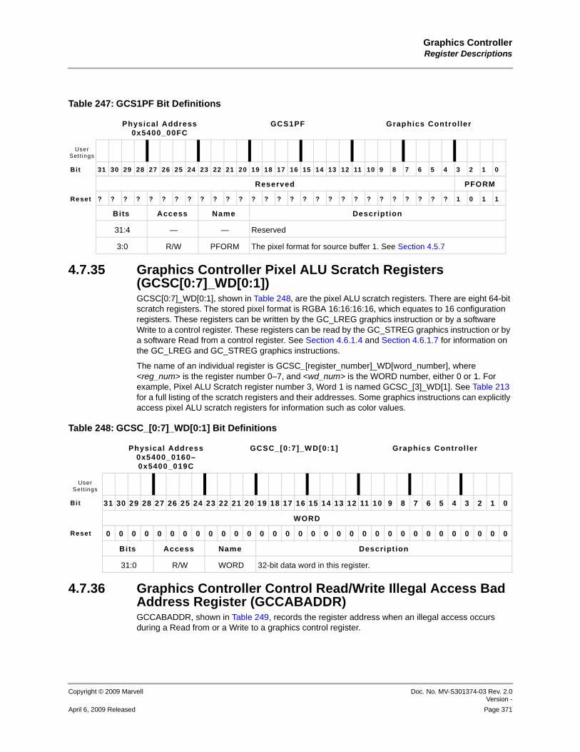
Graphics ControllerRegister Descriptions
Copyright © 2009 Marvell Doc. No. MV-S301374-03 Rev. 2.0Version -
April 6, 2009 Released Page 371
12345678910111213141516171819202122232425262728293031323334353637383940414243444546474849505152535455565758
4.7.35 Graphics Controller Pixel ALU Scratch Registers (GCSC[0:7]_WD[0:1])GCSC[0:7]_WD[0:1], shown in Table 248, are the pixel ALU scratch registers. There are eight 64-bit scratch registers. The stored pixel format is RGBA 16:16:16:16, which equates to 16 configuration registers. These registers can be written by the GC_LREG graphics instruction or by a software Write to a control register. These registers can be read by the GC_STREG graphics instruction or by a software Read from a control register. See Section 4.6.1.4 and Section 4.6.1.7 for information on the GC_LREG and GC_STREG graphics instructions.
The name of an individual register is GCSC_[register_number]_WD[word_number], where <reg_num> is the register number 0–7, and <wd_num> is the WORD number, either 0 or 1. For example, Pixel ALU Scratch register number 3, Word 1 is named GCSC_[3]_WD[1]. See Table 213 for a full listing of the scratch registers and their addresses. Some graphics instructions can explicitly access pixel ALU scratch registers for information such as color values.
4.7.36 Graphics Controller Control Read/Write Illegal Access Bad Address Register (GCCABADDR)GCCABADDR, shown in Table 249, records the register address when an illegal access occurs during a Read from or a Write to a graphics control register.
Table 247: GCS1PF Bit Definitions
Physical Address0x5400_00FC
GCS1PF Graphics Controller
User Sett ings
Bit 31 30 29 28 27 26 25 24 23 22 21 20 19 18 17 16 15 14 13 12 11 10 9 8 7 6 5 4 3 2 1 0
Reserved PFORM
Reset ? ? ? ? ? ? ? ? ? ? ? ? ? ? ? ? ? ? ? ? ? ? ? ? ? ? ? ? 1 0 1 1
Bits Access Name Descript ion
31:4 — — Reserved
3:0 R/W PFORM The pixel format for source buffer 1. See Section 4.5.7
Table 248: GCSC_[0:7]_WD[0:1] Bit Definitions
Physical Address0x5400_0160–0x5400_019C
GCSC_[0:7]_WD[0:1] Graphics Control ler
User Sett ings
Bit 31 30 29 28 27 26 25 24 23 22 21 20 19 18 17 16 15 14 13 12 11 10 9 8 7 6 5 4 3 2 1 0
WORD
Reset 0 0 0 0 0 0 0 0 0 0 0 0 0 0 0 0 0 0 0 0 0 0 0 0 0 0 0 0 0 0 0 0
Bits Access Name Descript ion
31:0 R/W WORD 32-bit data word in this register.
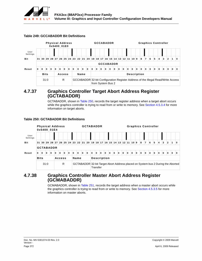
PXA3xx (88AP3xx) Processor FamilyVolume III: Graphics and Input Controller Configuration Developers Manual
Doc. No. MV-S301374-03 Rev. 2.0 Version -
Copyright © 2009 Marvell
Page 372 April 6, 2009 Released
12345678910111213141516171819202122232425262728293031323334353637383940414243444546474849505152535455565758
4.7.37 Graphics Controller Target Abort Address Register (GCTABADDR)GCTABADDR, shown in Table 250, records the target register address when a target abort occurs while the graphics controller is trying to read from or write to memory. See Section 4.5.3.4 for more information on target aborts.
4.7.38 Graphics Controller Master Abort Address Register (GCMABADDR)GCMABADDR, shown in Table 251, records the target address when a master abort occurs while the graphics controller is trying to read from or write to memory. See Section 4.5.3.5 for more information on master aborts.
Table 249: GCCABADDR Bit Definitions
Physical Address0x5400_01E0
GCCABADDR Graphics Controller
User Sett ings
Bit 31 30 29 28 27 26 25 24 23 22 21 20 19 18 17 16 15 14 13 12 11 10 9 8 7 6 5 4 3 2 1 0
GCCABADDR
Reset 0 0 0 0 0 0 0 0 0 0 0 0 0 0 0 0 0 0 0 0 0 0 0 0 0 0 0 0 0 0 0 0
Bits Access Name Descript ion
31:0 R GCCABADDR 32-bit Configuration Register Address of the Illegal Read/Write Access from System Bus 2
Table 250: GCTABADDR Bit Definitions
Physical Address0x5400_01E4
GCTABADDR Graphics Control ler
User Sett ings
Bit 31 30 29 28 27 26 25 24 23 22 21 20 19 18 17 16 15 14 13 12 11 10 9 8 7 6 5 4 3 2 1 0
GCTABADDR
Reset 0 0 0 0 0 0 0 0 0 0 0 0 0 0 0 0 0 0 0 0 0 0 0 0 0 0 0 0 0 0 0 0
Bits Access Name Descript ion
31:0 R GCTABADDR 32-bit Target Abort Address placed on System bus 2 During the Aborted Transfer
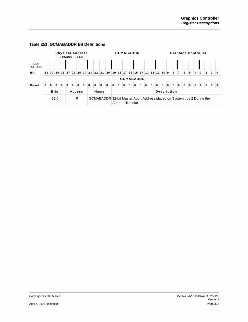
Graphics ControllerRegister Descriptions
Copyright © 2009 Marvell Doc. No. MV-S301374-03 Rev. 2.0Version -
April 6, 2009 Released Page 373
12345678910111213141516171819202122232425262728293031323334353637383940414243444546474849505152535455565758
Table 251: GCMABADDR Bit Definitions
Physical Address0x5400_01E8
GCMABADDR Graphics Controller
User Sett ings
Bit 31 30 29 28 27 26 25 24 23 22 21 20 19 18 17 16 15 14 13 12 11 10 9 8 7 6 5 4 3 2 1 0
GCMABADDR
Reset 0 0 0 0 0 0 0 0 0 0 0 0 0 0 0 0 0 0 0 0 0 0 0 0 0 0 0 0 0 0 0 0
Bits Access Name Descript ion
31:0 R GCMABADDR 32-bit Master Abort Address placed on System bus 2 During the Aborted Transfer

PXA3xx (88AP3xx) Processor FamilyVolume III: Graphics and Input Controller Configuration Developers Manual
Doc. No. MV-S301374-03 Rev. 2.0 Version -
Copyright © 2009 Marvell
Page 374 April 6, 2009 Released
12345678910111213141516171819202122232425262728293031323334353637383940414243444546474849505152535455565758

Keypad ControllerPXA3xx Processor Differences
Copyright © 2009 Marvell Doc. No. MV-S301374-03 Rev. 2.0Version -
April 6, 2009 Released Page 375
12345678910111213141516171819202122232425262728293031323334353637383940414243444546474849505152535455565758
5 Keypad ControllerThe keypad controller manages up to 8 × 8 matrix keys, up to eight direct keys, and up to two rotary encoders, which can implement scroll keys, jog-dials, and thumbwheels.The keypad controller provides an interface to two styles of keypads simultaneously through the matrix and direct keypad interface. The controller manages both manual and automatic scans.
Stable keypad activity that lasts longer than the debounce interval generates an interrupt. A manual matrix scan can then be conducted by setting appropriate bits in the Keypad Control register to assert the scan lines sequentially. The row readings for each column are read from the Keypad Matrix Key register as they are scanned. If the ignore-multiple-keypress (IMKP) bit is set in the Keypad Control register (KPC), only one interrupt is generated for a debounced keypress. For example, if three keys are pressed and held, only one interrupt is generated after the first key is pressed and held.
The column-scan signals are automatically asserted in sequence by the automatic scan logic in the keypad controller, and the row readings are stored in the automatic scan registers. Automatic scans can be initiated by either of the following methods:
If there is stable keypad activity for a period greater than the specified key debounce interval while the automatic-scan-on-activity (ASACT) bit in the KPC register is set, completion of the scan generates an interrupt.
If the automatic-scan (AS) bit is set, user software determines when to initiate an automatic scan. This option does not generate an interrupt.
5.1 PXA3xx Processor DifferencesTable 252 shows the keypad controller differences among the PXA32x, PXA31x and PXA30x processors.
5.2 FeaturesThe keypad controller is divided into two blocks: one for the matrix keypad and one for the direct keypad. The direct keys can be organized in three different ways:
Direct keypad:
• Up to eight direct key input signals with no rotary encoder
• Up to six direct keys and one rotary encoder
- DKIN<1:0> for the rotary encoder
• Up to four direct keys and two rotary encoders (PXA31x and PXA30x Only)
- DKIN<1:0> for rotary encoder A
- DKIN<3:2> for the rotary encoder B
Table 252: PXA3xx Processors Feature Differences
Feature PXA30x PXA31x PXA32x
Rotary Encoders 2 2 1

PXA3xx (88AP3xx) Processor FamilyVolume III: Graphics and Input Controller Configuration Developers Manual
Doc. No. MV-S301374-03 Rev. 2.0 Version -
Copyright © 2009 Marvell
Page 376 April 6, 2009 Released
12345678910111213141516171819202122232425262728293031323334353637383940414243444546474849505152535455565758
Note
Note To support one rotary encoder, two direct key inputs are used.
Matrix keypad:
• Eight scan output signals and eight input signals (returns)
• Up to 64 keys
• Manual or automatic scan
Simultaneous operation of direct keypad and matrix keypad
Interrupt generated on keypad activity:
• Separate matrix keypad and direct keypad interrupt enables
• One interrupt signal, generated by merging the matrix keypad interrupt and direct keypad interrupt
Continuous keypad pollingKey-debounce logic for both the matrix keypad and the direct keypad.
Note
Note Depending upon the GPIO alternate function configuration, not all of the keypad signals may be available for use. The GPIO alternate functions are shared with other peripherals.
5.3 SignalsThe interface signals (I/O) for the keypad controller are summarized in Table 253.
Table 253: Keypad Interface (I/O) Signals
Name Type Descript ion
KP_DKIN<7:0> Input Direct Key InputsSignals from the direct keys and the rotary-encoder sensor. KP_DKIN<7:4> are dedicated input signals for direct keys 7 through 4. KP_DKIN<1:0> are either input signals for direct keys 1 and 0 or input sensor signals for rotary encoder A (if enabled). KP_DKIN<3:2> are either input signals for direct keys 3 and 2 or input-sensor signals for rotary encoder B (if enabled).
KP_MKIN<7:0> Input Matrix Key Inputs (Returns)The input signals from the matrix keypad (matrix-keypad row readings).
KP_MKOUT<7:0> Output Matrix Key Column-Scan OutputsThe keypad controller sends column-scan output signals to the columns of the matrix keypad to detect any key(s) that are pressed. If an automatic scan is occurring, these column-scan output signals are driven by the automatic scan logic. At other times, they are driven by the settings of bits MS7 through MS0 in the Keypad Interface Control (KPC) register, see Table 255.
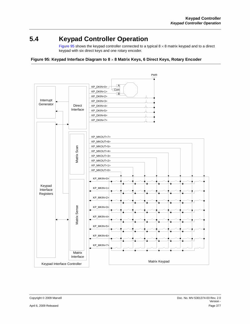
Keypad ControllerKeypad Controller Operation
Copyright © 2009 Marvell Doc. No. MV-S301374-03 Rev. 2.0Version -
April 6, 2009 Released Page 377
12345678910111213141516171819202122232425262728293031323334353637383940414243444546474849505152535455565758
5.4 Keypad Controller OperationFigure 95 shows the keypad controller connected to a typical 8 × 8 matrix keypad and to a direct keypad with six direct keys and one rotary encoder.
Figure 95: Keypad Interface Diagram to 8 × 8 Matrix Keys, 6 Direct Keys, Rotary Encoder
Com
Keypad Interface Controller
Matrix Interface
Mat
rix S
ense
Mat
rix S
can
Keypad Interface Registers
InterruptGenerator Direct
Interface
Matrix Keypad
KP_MKIN<0>
KP_MKIN<1>
KP_MKIN<2>
KP_MKIN<3>
KP_MKIN<4>
KP_MKIN<5>
KP_MKIN<6>
KP_MKIN<7>
KP_MKOUT<7>
KP_MKOUT<6>
KP_MKOUT<5>
KP_MKOUT<4>
KP_MKOUT<3>
KP_MKOUT<2>
KP_MKOUT<1>
KP_MKOUT<0>
PWR
KP_DKIN<2>
KP_DKIN<3>
KP_DKIN<4>
KP_DKIN<5>
KP_DKIN<0>
KP_DKIN<1>
A
B
KP_DKIN<6>
KP_DKIN<7>

PXA3xx (88AP3xx) Processor FamilyVolume III: Graphics and Input Controller Configuration Developers Manual
Doc. No. MV-S301374-03 Rev. 2.0 Version -
Copyright © 2009 Marvell
Page 378 April 6, 2009 Released
12345678910111213141516171819202122232425262728293031323334353637383940414243444546474849505152535455565758
5.4.1 Matrix Keypad InterfaceThe matrix-keypad interface outputs eight KP_MKOUT<7:0> column-scan signals to the columns of the matrix keypad and inputs eight KP_MKIN<7:0> sense signals from the rows of the matrix keypad. This 8 × 8 organization supports up to 64 keys. Up to eight scan signals, corresponding to columns in the matrix keypad, are sent to the keypad to activate the columns. Up to eight input (sense) signals, corresponding to rows in an activated column, are read into the following registers, depending on the mode of operation:
Manual scans: Keypad Matrix Key (KPMK) RegisterAutomatic scans: Keypad Interface Automatic Scan (KPAS) RegisterKeypad Interface Automatic Scan Multiple Keypress (KPASMKPx) Registers 0:3
The keypad controller requires pulldown resistors on the KP_MKOUT<7:0> and KP_MKIN<7:0> pins for correct operation of the matrix keypad interface. Software must internally enable these resistors in the pad ring. Software enables the pulldown resistors by setting the appropriate bits of the Multi-Function (MF) pin registers corresponding to the KP_MKOUT<7:0> and KP_MKIN<7:0> pins. For details on these registers and their use, refer to the multi-function pin chapter.
The matrix keypad block of the keypad controller has three scanning modes:
Manual scanAutomatic scan initiated by keypad activity
Automatic scan initiated by user software
5.4.1.1 Manual Matrix ScanTo enable manual matrix keypad scanning, configure the KPC register (shown and described in Table 255) as follows:
1. Clear the automatic-scan-on-activity (ASACT) bit.2. Clear the automatic-scan AS bit.3. Assert all column (scan output) lines by setting the MS[7:0] bits.
In this Polling mode of operation, all keypad columns remain constantly activated. Any keypress that exceeds the key-debounce interval generates an interrupt. Service the interrupt as follows:
1. De-assert all of the columns by clearing bits MS[7:0].2. Sequentially set the MS[7:0] bits to scan all keypad columns. 3. As the columns are scanned, read each column row (scan input) value, which appears in bits
KPMK[MR7:0] (see Table 258).4. After servicing the interrupt, assert all column (scan output) lines by setting bits KPC[MS7:0]
(see Table 255).This positions the scanning logic to detect the next keypress.
Depending on whether the ignore-multiple-keypress (IMKP) bit is set or cleared, manual scan and automatic scan on keypad activity occurs as follows:
Ignore multiple keypress (IMKP set). Multiple keypresses are ignored and not considered as new keypad activity. For example, if an automatic scan is conducted for a keypress activity, another automatic scan is not conducted until all keys are released.Do not ignore multiple keypress (IMKP cleared). For automatic scan on keypad activity, an automatic scan is conducted after a debounce interval for all of the time that:
• One or more keys are pressed (new activity).
• All keys are released.
An interrupt is generated if the scanned activity is new.

Keypad ControllerKeypad Controller Operation
Copyright © 2009 Marvell Doc. No. MV-S301374-03 Rev. 2.0Version -
April 6, 2009 Released Page 379
12345678910111213141516171819202122232425262728293031323334353637383940414243444546474849505152535455565758
5.4.1.2 Automatic Matrix Scan Initiated by Keypad ActivityTo enable automatic matrix keypad scanning initiated by keypad activity:
1. Set the automatic-scan-on-activity KPC[ASACT] (see Table 255).2. Clear the automatic-scan KPC[AS] bit, (see Table 255).
In this Polling mode of operation, the value of the ignore-multiple-keypress KPC[IMKP] bit (see Table 255) defines keypress activity. An interrupt is generated after the automatic scan completes if new keypad activity is detected.
The KPAS[MUKP] bit field identifies whether a single key or multiple keys were pressed. For single keypresses, read the column and row information directly from KPAS[CP] (bits 3:0) and KPAS[RP] (bits 7:4). For multiple keypresses, read the column and row information from the KPASMKPx registers (see Section 5.5.6).
5.4.1.3 Automatic Matrix Scan Initiated By SoftwareTo enable automatic matrix-keypad scanning initiated by user software, set the automatic-scan KPC[AS] bit. In this mode of operation, the keypad is scanned only once, and the row readings are stored in the Keypad Interface Automatic Scan (KPAS) Register and the Keypad Interface Automatic Scan Multiple Keypress (KPASMKPx) Registers 0:3. No interrupt is generated because user software initiates the scan.
5.4.2 Direct-Key InterfaceThe direct-key interface receives the KP_DKIN<7:0> input signals from a combination of up to eight direct keys and up to two rotary encoder and stores them in the Keypad Direct Key (KPDK) Register. When the direct-key block of the keypad controller detects debounced activity in the direct keys or the rotary encoders, it sets the KPC[DI] bit to cause a keypad interrupt.
Two options are available for the direct key and rotary encoder debounce intervals, depending on the state of the KCP direct-keypad-debounce-select DK_DEB_SEL bit:
Regular debounce interval, DK_DEB_SEL = 0. This is the default debounce interval. The direct-key debounce interval is the same as the matrix-key debounce interval field of the KPKDI register. The rotary-encoder debounce interval can be either the matrix key debounce interval or zero, depending on the state of the rotary-encoder zero-debounce RE_ZERO_DEB select bit of the Keypad Control (KPC) Register.Direct-key debounce interval, DK_DEB_SEL = 1. Specified in the direct-key debounce interval field of the Keypad Key-Debounce Interval (KPKDI) Register. This is the debounce interval for the direct key and rotary-encoder logic. The rotary-encoder debounce interval can be either the direct-key debounce interval or zero, depending on the state of the rotary-encoder zero-debounce select bit (RE_ZERO_DEB) of the KPC register.
It is not necessary for every direct-key input to be connected to the keypad interface if the corresponding GPIO pins are in use as inputs or outputs for other blocks. For example, if GPIO pins corresponding to direct-key inputs 2 and 3 are used as inputs/outputs for other blocks, they are unavailable for the keypad interface. The KP_DKIN<3:2> input signals are guaranteed to be logic 0 at all times, which means that no activity is detected for direct keys 2 and 3. Software uses the remaining direct-key inputs, KP_DKIN<1:0> and KP_DKIN<7:4>, that are connected to either a rotary encoder or direct keys by specifying the number of direct keys in the Keypad Control register as eight (KPC[DKN] = 0b111). Although the direct-key inputs 2 and 3 are used for other applications, the keypad controller always detects no activity on them.
5.4.2.1 Direct KeysThe direct-key interface reads up to eight direct keys and stores them in the Keypad Direct Key (KPDK) Register. Power and reset keys can be implemented as direct keys.

PXA3xx (88AP3xx) Processor FamilyVolume III: Graphics and Input Controller Configuration Developers Manual
Doc. No. MV-S301374-03 Rev. 2.0 Version -
Copyright © 2009 Marvell
Page 380 April 6, 2009 Released
12345678910111213141516171819202122232425262728293031323334353637383940414243444546474849505152535455565758
5.4.2.2 Rotary EncodersA rotary encoder consists of a cylindrical rotor with metal strips and a pair of sensors (see Figure 96). It can implement items such as scroll keys, jog dials, and thumbwheels. The direct-key interface supports one rotary encoder and stores the sensor outputs in KPDK[1:0] (see Table 256).
5.4.3 Debounce CheckThe debounce intervals for the matrix keys and direct keys are specified in the Keypad Key-Debounce Interval (KPKDI) Register. Clear all bits in the KPKDI[Interval] fields to disable debounce checking. In practice, the minimum value to use for the debounce interval is 10 ms. The input signals, direct or matrix, are considered debounced if they remain stable for the debounce intervals specified in KPKDI[Interval]. The optimum debounce interval depends on the type of keypad and the Scan mode. See Section 5.5.7 for details on the intervals available.
The rotary encoder debounce interval is equal to the direct keypad debounce interval unless KPC[RE_ZERO_DEB] = 1 (see Table 255), in which case the rotary encoder debounce interval is zero.
The following debouncing procedures, described here to clarify operation, occur transparently. No action is required by user software.
5.4.3.1 Matrix Keypad, Manual Scan ProcedureIn manual-matrix scan, only the keypress or no-keypress information is detected and stored. The user software must scan the entire keypad to determine the individual states of all keys:
1. Read the matrix keypad inputs and determine whether any key(s) or no keys are pressed.2. Wait one debounce interval.
3. Read the matrix keypad inputs again and determine whether any key(s) or no keys are pressed.If the results from the two successive reads match, the keys are debounced. Otherwise, repeat steps 2 and 3 until two successive reads match.
Figure 96: Rotary Encoder
Rotary Encoder
Sensor_A
Conductive Metal
Rotor
Sensor_B
Scroll_Up
Scroll_Dn

Keypad ControllerKeypad Controller Operation
Copyright © 2009 Marvell Doc. No. MV-S301374-03 Rev. 2.0Version -
April 6, 2009 Released Page 381
12345678910111213141516171819202122232425262728293031323334353637383940414243444546474849505152535455565758
5.4.3.2 Matrix Keypad, Automatic Scan ProcedureThe debounce check occurs only for automatic scans initiated by keypad activity (KPC[ASACT] set), not for automatic scans initiated by setting KPC[AS]:
1. Automatically conduct a full scan of the matrix keypad to obtain the state of all keys.
2. Automatically wait one debounce interval.3. Automatically conduct another full scan of the matrix keypad to obtain the state of all keys.
If the results from the two successive scans match, the keys are debounced. Otherwise, automatically repeat steps 2 and 3 until two successive scans match.
5.4.3.3 Direct Keypad ProcedureThe direct keypad procedure is as follows:
1. Read the direct keypad inputs.
2. Wait one debounce interval.3. Read the direct keypad inputs again.
If the results from the two successive reads match, the keys are debounced. Otherwise, repeat steps 2 and 3 until two successive reads match.
5.4.4 Interrupt GenerationThe keypad-controller interrupt is generated by merging the matrix-keypad interrupt KPC[MI] and the direct-keypad interrupt KPC[DI]. Use the matrix-keypad interrupt-enable bit KPC[MIE] and the direct-keypad interrupt-enable bit KPC[DIE] to enable/disable each type of interrupt. The following sections describe interrupt generation:
Section 5.4.1.1, Manual Matrix ScanSection 5.4.1.2, Automatic Matrix Scan Initiated by Keypad Activity
Section 5.4.1.3, Automatic Matrix Scan Initiated By SoftwareSection 5.4.2, Direct-Key Interface
5.4.5 Low Power Operation and WakeupThe keypad and the connected multi-function pins in the pad-ring can wake up the processor from various low-power states. This detection occurs in the pad-ring itself and uses the edge detectors there, reporting back to the APMU through one of the keypad or generic wakeup functions. This function is described in the Slave Power Management Unit chapter in Volume I of this manual.
A wakeup detection causes the processor to transition to a run state. It does not necessarily identify which function caused the transition. However, the keypad performs the normal actions during Run mode when it exits the low-power state, which causes an interrupt and identifies the pressed key if the relevant key is still pressed (the same applies to the rotary encoder functions).
A typical scenario is as follows:
1. In a low-power state, the enabled MKOUT pins are driven high through the low-power state in the pad-ring.
The MKIN signals are inputs with pulldown resistors. If the MKOUT pins are de-asserted, the MKIN pins cannot be used to generate a wakeup.
2. A matrix key is pressed, which causes a transition on the KPIN wires from low to high that provokes a wakeup to be detected in the pad-ring and reported to the PMU.
3. The processor transitions to a run state.
4. The keypad controller can either be completely reset (S2/D3/C4 exit) or still configured:
• If the controller is reset, software can reconfigure the controller quickly and it behaves as if a key was just pressed by performing a scan (if KPC[ASACT] is set).
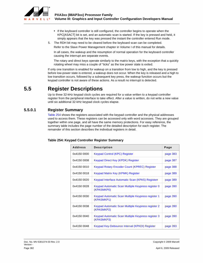
PXA3xx (88AP3xx) Processor FamilyVolume III: Graphics and Input Controller Configuration Developers Manual
Doc. No. MV-S301374-03 Rev. 2.0 Version -
Copyright © 2009 Marvell
Page 382 April 6, 2009 Released
12345678910111213141516171819202122232425262728293031323334353637383940414243444546474849505152535455565758
• If the keyboard controller is still configured, the controller begins to operate when the KPC[ASACT] bit is set, and an automatic scan is started. If the key is pressed and held, it simply appears that the key was pressed the instant the controller entered Run mode.
5. The RDH bit may need to be cleared before the keyboard scan can be completed.Refer to the Slave Power Management chapter in Volume I of this manual for details.
In all cases, the wakeup and the resumption of normal operation for the keyboard controller causing the interrupt are separate events.
The rotary and direct keys operate similarly to the matrix keys, with the exception that a quickly rotating wheel may miss a couple of “ticks” as the low power state is exited.
If only one transition is enabled for wakeup on a transition from low to high, and the key is pressed before low-power state is entered, a wakeup does not occur. When the key is released and a high to low transition occurs, followed by a subsequent key press, the wakeup function occurs but the keypad controller is not aware of these actions. As a result no interrupt is detected.
5.5 Register DescriptionsUp to three 32-kHz keypad clock cycles are required for a value written to a keypad controller register from the peripheral interface to take effect. After a value is written, do not write a new value until six additional 32-kHz keypad clock cycles elapse.
5.5.0.1 Register SummaryTable 254 shows the registers associated with the keypad controller and the physical addresses used to access them. These registers can be accessed only with word accesses. They are grouped together within one page, and all have the same memory protections. For easy reference, the summary table includes the page number of the detailed description for each register. The remainder of this section describes the individual registers in detail.
Table 254: Keypad Controller Register Summary
Address Descript ion Page
0x4150 0000 Keypad Control (KPC) Register page 383
0x4150 0008 Keypad Direct Key (KPDK) Register page 387
0x4150 0010 Keypad Rotary Encoder Count (KPREC) Register page 388
0x4150 0018 Keypad Matrix Key (KPMK) Register page 389
0x4150 0020 Keypad Interface Automatic Scan (KPAS) Registerr page 389
0x4150 0028 Keypad Automatic Scan Multiple Keypress register 0 (KPASMKP0)
page 390
0x4150 0030 Keypad Automatic Scan Multiple Keypress register 1 (KPASMKP1)
page 390
0x4150 0038 Keypad Automatic Scan Multiple Keypress register 2 (KPASMKP2)
page 390
0x4150 0040 Keypad Automatic Scan Multiple Keypress register 3 (KPASMKP3)
page 390
0x4150 0048 Keypad Key-Debounce Interval (KPKDI) Register page 393
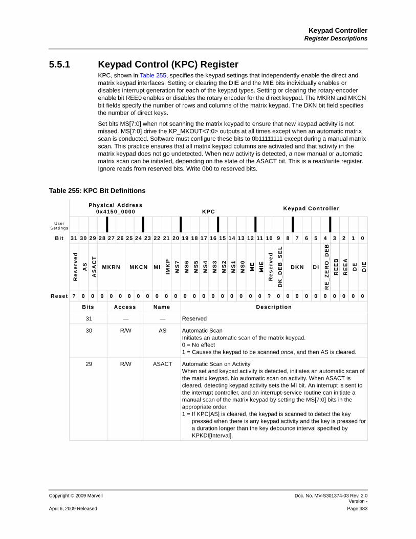
Keypad ControllerRegister Descriptions
Copyright © 2009 Marvell Doc. No. MV-S301374-03 Rev. 2.0Version -
April 6, 2009 Released Page 383
12345678910111213141516171819202122232425262728293031323334353637383940414243444546474849505152535455565758
5.5.1 Keypad Control (KPC) RegisterKPC, shown in Table 255, specifies the keypad settings that independently enable the direct and matrix keypad interfaces. Setting or clearing the DIE and the MIE bits individually enables or disables interrupt generation for each of the keypad types. Setting or clearing the rotary-encoder enable bit REE0 enables or disables the rotary encoder for the direct keypad. The MKRN and MKCN bit fields specify the number of rows and columns of the matrix keypad. The DKN bit field specifies the number of direct keys.
Set bits MS[7:0] when not scanning the matrix keypad to ensure that new keypad activity is not missed. MS[7:0] drive the KP_MKOUT<7:0> outputs at all times except when an automatic matrix scan is conducted. Software must configure these bits to 0b11111111 except during a manual matrix scan. This practice ensures that all matrix keypad columns are activated and that activity in the matrix keypad does not go undetected. When new activity is detected, a new manual or automatic matrix scan can be initiated, depending on the state of the ASACT bit. This is a read/write register. Ignore reads from reserved bits. Write 0b0 to reserved bits.
Table 255: KPC Bit Definitions
Physical Address0x4150_0000 KPC Keypad Controller
User Sett ings
Bit 31 30 29 28 27 26 25 24 23 22 21 20 19 18 17 16 15 14 13 12 11 10 9 8 7 6 5 4 3 2 1 0
Re
se
rve
d
AS
AS
AC
T
MKRN MKCN MI
IMK
P
MS
7
MS
6
MS
5
MS
4
MS
3
MS
2
MS
1
MS
0
ME
MIE
Re
se
rve
d
DK
_D
EB
_S
EL
DKN DI
RE
_Z
ER
O_
DE
B
RE
EB
RE
EA
DE
DIE
Reset ? 0 0 0 0 0 0 0 0 0 0 0 0 0 0 0 0 0 0 0 0 ? 0 0 0 0 0 0 0 0 0 0
Bits Access Name Descript ion
31 — — Reserved
30 R/W AS Automatic ScanInitiates an automatic scan of the matrix keypad. 0 = No effect1 = Causes the keypad to be scanned once, and then AS is cleared.
29 R/W ASACT Automatic Scan on ActivityWhen set and keypad activity is detected, initiates an automatic scan of the matrix keypad. No automatic scan on activity. When ASACT is cleared, detecting keypad activity sets the MI bit. An interrupt is sent to the interrupt controller, and an interrupt-service routine can initiate a manual scan of the matrix keypad by setting the MS[7:0] bits in the appropriate order.1 = If KPC[AS] is cleared, the keypad is scanned to detect the key
pressed when there is any keypad activity and the key is pressed for a duration longer than the key debounce interval specified by KPKDI[Interval].

PXA3xx (88AP3xx) Processor FamilyVolume III: Graphics and Input Controller Configuration Developers Manual
Doc. No. MV-S301374-03 Rev. 2.0 Version -
Copyright © 2009 Marvell
Page 384 April 6, 2009 Released
12345678910111213141516171819202122232425262728293031323334353637383940414243444546474849505152535455565758
28:26 R/W MKRN Matrix Keypad Row NumberThis octal value plus 1 indicates the number of rows in the matrix keypad. Examples:000 = Number of keypad rows = 1111 = Number of keypad rows = 8
25:23 R/W MKCN Matrix Keypad Column NumberThis octal value plus 1 indicates the number of columns in the matrix keypad. Examples:000 = Number of keypad columns = 1111 = Number of keypad columns = 8
22 R MI Matrix Keypad InterruptWhen MI is automatically set, an interrupt is sent to the interrupt controller. MI is reset when read. Writes to MI are ignored.
21 R/W IMKP Ignore Multiple Keypress (applies only to the matrix-keypad interface)If set for the matrix keypad, multiple keypresses are ignored. Only when all keys are released is a new scan initiated to detect activity (for an automatic scan by keypad activity) or an interrupt generated (for a manual scan).0 = For either an automatic scan by keypad activity or a manual scan, do
not ignore multiple keypresses.1 = For either an automatic scan by keypad activity or a manual scan,
ignore multiple keypresses after a keypress activity has been detected and scanned.
20 R/W MS7† Manual Matrix Scan line 7: asserted to scan column 7 of the matrix keypad.
19 R/W MS6† Manual Matrix Scan line 6: asserted to scan column 6 of the matrix keypad.
18 R/W MS5† Manual Matrix Scan line 5: asserted to scan column 5 of the matrix keypad.
17 R/W MS4† Manual Matrix Scan line 4: asserted to scan column 4 of the matrix keypad.
16 R/W MS3† Manual Matrix Scan line 3: asserted to scan column 3 of the matrix keypad.
Table 255: KPC Bit Definitions (Continued)
Physical Address0x4150_0000 KPC
Keypad Controller
User Sett ings
Bit 31 30 29 28 27 26 25 24 23 22 21 20 19 18 17 16 15 14 13 12 11 10 9 8 7 6 5 4 3 2 1 0
Re
se
rve
d
AS
AS
AC
T
MKRN MKCN MI
IMK
P
MS
7
MS
6
MS
5
MS
4
MS
3
MS
2
MS
1
MS
0
ME
MIE
Re
se
rve
d
DK
_D
EB
_S
EL
DKN DI
RE
_Z
ER
O_
DE
B
RE
EB
RE
EA
DE
DIE
Reset ? 0 0 0 0 0 0 0 0 0 0 0 0 0 0 0 0 0 0 0 0 ? 0 0 0 0 0 0 0 0 0 0
Bits Access Name Descript ion

Keypad ControllerRegister Descriptions
Copyright © 2009 Marvell Doc. No. MV-S301374-03 Rev. 2.0Version -
April 6, 2009 Released Page 385
12345678910111213141516171819202122232425262728293031323334353637383940414243444546474849505152535455565758
15 R/W MS2† Manual Matrix Scan line 2: asserted to scan column 2 of the matrix keypad.
14 R/W MS1† Manual Matrix Scan line 1: asserted to scan column 1 of the matrix keypad.
13 R/W MS0† Manual Matrix Scan line 0: asserted to scan column 0 of the matrix keypad.
12 R/W ME Matrix Keypad Enable0 = Disabled1 = Enabled
11 R/W MIE Matrix Interrupt Enable0 = Disabled1 = Enabled
10 — Reserved Reserved
9 R/W DK_DEB_SEL
Direct Keypad Debounce SelectDK_DEB_SEL = 1: Direct keypad debounce interval equal to the direct key debounce interval field of the KPKDI register.DK_DEB_SEL = 0: Direct keypad debounce interval equal to the matrix key debounce interval field of the KPKDI register.
8:6 R/W DKN Direct Key NumberThis octal value + 1 indicates the number of keys in the direct keypad plus the number of rotary-encoder sensor inputs. Examples:000 = Number of direct keys plus rotary-encoder sensor inputs = 1111 = Number of direct keys plus rotary-encoder sensor inputs = 8
5 R DI Direct Keypad InterruptActivity detected in the direct keypad or the rotary encoders automatically sets DI. The keypad interrupt is sent to the interrupt controller, the direct-key interrupt-service routine is initiated, and the Direct Key (KPDK) register is read to determine the key(s) that are pressed.
4 R/W RE_ZERO_DEB
Rotary Encoder Zero Debounce Interval0 = Rotary encoder logic debounce interval is equal to the direct keypad
debounce interval.1 = Rotary encoder logic debounce interval equals zero.
Table 255: KPC Bit Definitions (Continued)
Physical Address0x4150_0000 KPC
Keypad Controller
User Sett ings
Bit 31 30 29 28 27 26 25 24 23 22 21 20 19 18 17 16 15 14 13 12 11 10 9 8 7 6 5 4 3 2 1 0
Re
se
rve
d
AS
AS
AC
T
MKRN MKCN MI
IMK
P
MS
7
MS
6
MS
5
MS
4
MS
3
MS
2
MS
1
MS
0
ME
MIE
Re
se
rve
d
DK
_D
EB
_S
EL
DKN DI
RE
_Z
ER
O_
DE
B
RE
EB
RE
EA
DE
DIE
Reset ? 0 0 0 0 0 0 0 0 0 0 0 0 0 0 0 0 0 0 0 0 ? 0 0 0 0 0 0 0 0 0 0
Bits Access Name Descript ion

PXA3xx (88AP3xx) Processor FamilyVolume III: Graphics and Input Controller Configuration Developers Manual
Doc. No. MV-S301374-03 Rev. 2.0 Version -
Copyright © 2009 Marvell
Page 386 April 6, 2009 Released
12345678910111213141516171819202122232425262728293031323334353637383940414243444546474849505152535455565758
3 R/W REEB Rotary Encoder B Enable0 = Not enabled1 = Enabled
2 R/W REEA Rotary Encoder A Enable0 = Disabled1 = Enabled
1 R/W DE Direct Keypad Enable0 = Disabled1 = Enabled
0 R/W DIE Direct Keypad Interrupt Enable0 = Disabled1 = Enabled
† All of the KPC[MS7:MS0] bits must be set simultaneously to detect matrix keypad activity correctly.
Table 255: KPC Bit Definitions (Continued)
Physical Address0x4150_0000 KPC
Keypad Controller
User Sett ings
Bit 31 30 29 28 27 26 25 24 23 22 21 20 19 18 17 16 15 14 13 12 11 10 9 8 7 6 5 4 3 2 1 0
Re
se
rve
d
AS
AS
AC
T
MKRN MKCN MI
IMK
P
MS
7
MS
6
MS
5
MS
4
MS
3
MS
2
MS
1
MS
0
ME
MIE
Re
se
rve
d
DK
_D
EB
_S
EL
DKN DI
RE
_Z
ER
O_
DE
B
RE
EB
RE
EA
DE
DIE
Reset ? 0 0 0 0 0 0 0 0 0 0 0 0 0 0 0 0 0 0 0 0 ? 0 0 0 0 0 0 0 0 0 0
Bits Access Name Descript ion

Keypad ControllerRegister Descriptions
Copyright © 2009 Marvell Doc. No. MV-S301374-03 Rev. 2.0Version -
April 6, 2009 Released Page 387
12345678910111213141516171819202122232425262728293031323334353637383940414243444546474849505152535455565758
5.5.2 Keypad Direct Key (KPDK) RegisterKPDK, shown in Table 256, contains details of the last read of the direct keypad inputs KP_DKIN<7:0> if the direct keypad is enabled by setting the KPC[DE] bit. The status of all of the direct keys is stored in KPDK on each read of the direct keypad. This register is reset only on power-up. This is a read-only register. Ignore reads from reserved bits.
Table 256: KPDK Bit Definitions
Physical Address0x4150_0008 KPDK
Keypad Control ler
User Sett ings
Bit 31 30 29 28 27 26 25 24 23 22 21 20 19 18 17 16 15 14 13 12 11 10 9 8 7 6 5 4 3 2 1 0
DK
P
Reserved
DK
7
DK
6
DK
5
DK
4
RB
1-D
K3
RA
1-D
K2
RB
0-D
K1
RA
0-D
K0
Reset 0 ? ? ? ? ? ? ? ? ? ? ? ? ? ? ? ? ? ? ? ? ? ? ? 0 0 0 0 0 0 0 0
Bits Access Name Descript ion
31 RO DKP Direct Key Pressed0 = Reset on register read1 = Direct key pressed since last read
30:8 — — Reserved
7 RO DK7 Direct Key 7 input
6 RO DK6 Direct Key 6 input
5 RO DK5 Direct Key 5 input
4 RO DK4 Direct Key 4 input
3 RO RB1-DK3 Rotary Encoder B/Direct Key 3 inputIf rotary encoder 1 is disabled: input = direct key 3If rotary encoder 1 is enabled: input = rotary encoder 1, sensor B
2 RO RA1-DK2 Rotary Encoder A / Direct Key 2 inputIf rotary encoder 1 is disabled: input = direct key 2If rotary encoder 1 is enabled: input = rotary encoder 1, sensor A
1 RO RB0-DK1 Rotary Encoder B / Direct Key 1 inputIf rotary encoder 0 is disabled: input = direct key 1If rotary encoder 0 is enabled: input = rotary encoder 0, sensor B
0 RO RA0-DK0 Rotary Encoder A / Direct Key 0 inputIf rotary encoder 0 is disabled: input = direct key 0If rotary encoder 0 is enabled: input = rotary encoder 0, sensor A

PXA3xx (88AP3xx) Processor FamilyVolume III: Graphics and Input Controller Configuration Developers Manual
Doc. No. MV-S301374-03 Rev. 2.0 Version -
Copyright © 2009 Marvell
Page 388 April 6, 2009 Released
12345678910111213141516171819202122232425262728293031323334353637383940414243444546474849505152535455565758
5.5.3 Keypad Rotary Encoder Count (KPREC) RegisterKPREC, shown in Table 257, stores the value of the counter pertaining to the rotary encoder. This count value indicates any activity in the keys implemented using the rotary encoder. For example, with a scroll key, any activity increments or decrements the rotary encoder counter, depending on the direction of the scroll. This count value is stored in the KPREC register every 32 kHz keypad clock. Software must periodically read the count value and compare it with the last value read to determine the direction and magnitude of the scroll.
The KPREC register can store up to two 8-bit count values with an overflow and an underflow bit corresponding to each of the two counts. The underflow bits ([UFx0) are set when the count goes below zero. The overflow bits (OFx0) are set when the count goes beyond the maximum 8-bit value of 255. The overflow and underflow bits are reset when the KPREC register is read. This is a read/write register. Ignore reads from reserved bits. Write 0b0 to reserved bits.
Table 257: KPREC Bit Definitions
Physical Address0x4150_0010
KPREC Keypad Controller
User Sett ings
Bit 31 30 29 28 27 26 25 24 23 22 21 20 19 18 17 16 15 14 13 12 11 10 9 8 7 6 5 4 3 2 1 0
OF
B
UF
B
Reserved RE CountB
OF
A
UF
AReserved RE CountA
Reset 0 0 ? ? ? ? ? ? 0 0 0 0 0 0 0 0 0 0 ? ? ? ? ? ? 0 0 0 0 0 0 0 0
Bits Access Name Descript ion
31 R/W OFB Overflow Bit for Rotary Encoder BSet when the count value goes above the maximum 8-bit value of 255. Reset to 0b0 on read.
30 R/W UFB Underflow Bit for Rotary Encoder BSet when the count value goes below zero. Reset to 0b0 on read.
29:24 — — Reserved
23:16 RE CountB Count value for rotary encoder B.
15 R/W OFA Overflow Bit for Rotary Encoder ASet when the count value goes above the maximum 8-bit value of 255. Reset to 0b0 on read.
14 R/W UFA Underflow Bit for Rotary Encoder ASet when the count value goes below zero. Reset to 0b0 on read.
13:8 — — Reserved
7:0 R/W RE CountA Count value for rotary encoder 0.

Keypad ControllerRegister Descriptions
Copyright © 2009 Marvell Doc. No. MV-S301374-03 Rev. 2.0Version -
April 6, 2009 Released Page 389
12345678910111213141516171819202122232425262728293031323334353637383940414243444546474849505152535455565758
5.5.4 Keypad Matrix Key (KPMK) RegisterKPMK, shown in Table 258, contains the row details of the keys pressed on the matrix keypad when the last manual scan completes. When set, the MKP bit indicates that a matrix key was pressed since the register was last read. This is a read-only register. Ignore reads from reserved bits.
5.5.5 Keypad Interface Automatic Scan (KPAS) RegisterKPAS, shown in Table 259, contains row and column details for a single keypress or information about multiple keypresses or invalid data. An automatic scan of the keypad is initiated either for stable keypad activity longer than the key debounce interval while the KPC[ASACT] bit is set or when the KPC[AS] bit is set. Key presses, or the lack of them, affect bits in this register as follows:
If no key is pressed, the multiple-keys-pressed (MUKP) field contains the value 0b00000.
If a single key is pressed, the row and column details of the key are stored in the RP and CP bit fields. The MUKP bit field contains the value 0b00001.
If multiple keys are pressed, the MUKP bit field contains a value greater than 0b00001. Read the details on the keys pressed from the Keypad Interface Automatic Scan Multiple Keypress (KPASMKP0:3) registers.When the scan-on (SO) bit is set, a scan is in progress and the data in this register is invalid.
This is a read-only register. Ignore reads from reserved bits.
Table 258: KPMK Bit Definitions
Physical Address0x4150_0018
KPMK Keypad Control ler
User Sett ings
Bit 31 30 29 28 27 26 25 24 23 22 21 20 19 18 17 16 15 14 13 12 11 10 9 8 7 6 5 4 3 2 1 0
MK
P
Reserved
MR
7
MR
6
MR
5
MR
4
MR
3
MR
2
MR
1
MR
0
Reset 0 ? ? ? ? ? ? ? ? ? ? ? ? ? ? ? ? ? ? ? ? ? ? ? 0 0 0 0 0 0 0 0
Bits Access Name Descript ion
31 RO MKP 0 = Reset on register read1 = Matrix key pressed since last read
30:8 — — Reserved
7 RO MR7 Matrix Row 7
6 RO MR6 Matrix Row 6
5 RO MR5 Matrix Row 5
4 RO MR4 Matrix Row 4
3 RO MR3 Matrix Row 3
2 RO MR2 Matrix Row 2
1 RO MR1 Matrix Row 1
0 RO MR0 Matrix Row 0

PXA3xx (88AP3xx) Processor FamilyVolume III: Graphics and Input Controller Configuration Developers Manual
Doc. No. MV-S301374-03 Rev. 2.0 Version -
Copyright © 2009 Marvell
Page 390 April 6, 2009 Released
12345678910111213141516171819202122232425262728293031323334353637383940414243444546474849505152535455565758
5.5.6 Keypad Interface Automatic Scan Multiple Keypress (KPASMKPx) Registers 0:3KPASMKPx contain details of the row readings from automatic scans when multiple keys are pressed. Each register deals with two keypad columns.
5.5.6.1 Keypad Automatic Scan Multiple Keypress register 0 (KPASMKP0)KPASMKP0, shown in Table 260, contain details of the row readings from automatic scans when multiple keys are pressed. KPASMKP0 handles with keypad columns 1 - 0.
5.5.6.2 Keypad Automatic Scan Multiple Keypress register 1 (KPASMKP1)KPASMKP1, shown in Table 261, contain details of the row readings from automatic scans when multiple keys are pressed. KPASMKP1 handles with keypad columns 3 - 2.
Table 259: KPAS Bit Definitions
Physical Address0x4150_0020 KPAS Keypad Interface
User Settings
Bit 31 30 29 28 27 26 25 24 23 22 21 20 19 18 17 16 15 14 13 12 11 10 9 8 7 6 5 4 3 2 1 0
SO MUKP Reserved RP CP
Reset 0 0 0 0 0 0 ? ? ? ? ? ? ? ? ? ? ? ? ? ? ? ? ? ? 1 1 1 1 1 1 1 1
Bits Access Name Descript ion
31 RO SO Scan OnSet at the beginning of the automatic scan or automatic scan on activity and is cleared when the scan completes. When set, the data in this register is invalid.
30:26 RO MUKP Multiple Keys Pressed0b00000 = No key pressed.0b00001 = Single key pressed. Read row and column information from the RP and CP bit fields.>0b00001 = Multiple keys pressed. Read the keypress information from the KPASMKP0, KPASMKP1, KPASMKP2 and KPASMKP3 registers.
25:8 — — Reserved
7:4 RO RP Row Pressed 0b1111 = Data invalid (also the reset value)0b0000 = Key pressed is in row 0...continuing sequentially through...0b0111 = Key pressed is in row 7
3:0 RO CP Column Pressed0b1111 = Data invalid (also the reset value)0b0000 = Key pressed is in column 0...continuing sequentially through...0b0111 = Key pressed is in column 7
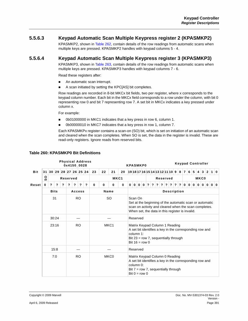
Keypad ControllerRegister Descriptions
Copyright © 2009 Marvell Doc. No. MV-S301374-03 Rev. 2.0Version -
April 6, 2009 Released Page 391
12345678910111213141516171819202122232425262728293031323334353637383940414243444546474849505152535455565758
5.5.6.3 Keypad Automatic Scan Multiple Keypress register 2 (KPASMKP2)KPASMKP2, shown in Table 262, contain details of the row readings from automatic scans when multiple keys are pressed. KPASMKP2 handles with keypad columns 5 - 4.
5.5.6.4 Keypad Automatic Scan Multiple Keypress register 3 (KPASMKP3)KPASMKP3, shown in Table 263, contain details of the row readings from automatic scans when multiple keys are pressed. KPASMKP3 handles with keypad columns 7 - 6.
Read these registers after:
An automatic scan interrupt.
A scan initiated by setting the KPC[AS] bit completes.
Row readings are recorded in 8-bit MKCx bit fields, two per register, where x corresponds to the keypad column number. Each bit in the MKCx field corresponds to a row under the column, with bit 0 representing row 0 and bit 7 representing row 7. A set bit in MKCx indicates a key pressed under column x.
For example:
0b01000000 in MKC1 indicates that a key press in row 6, column 1.
0b00000010 in MKC7 indicates that a key press in row 1, column 7.
Each KPASMKPx register contains a scan-on (SO) bit, which is set on initiation of an automatic scan and cleared when the scan completes. When SO is set, the data in the register is invalid. These are read-only registers. Ignore reads from reserved bits.
Table 260: KPASMKP0 Bit Definitions
Physical Address0x4150_0028 KPASMKP0
Keypad Controller
Bit 31 30 29 28 27 26 25 24 23 22 21 20 19 18 17 16 15 14 13 12 11 10 9 8 7 6 5 4 3 2 1 0
SO Reserved MKC1 Reserved MKC0
Reset 0 ? ? ? ? ? ? ? 0 0 0 0 0 0 0 0 ? ? ? ? ? ? ? ? 0 0 0 0 0 0 0 0
Bits Access Name Descript ion
31 RO SO Scan OnSet at the beginning of the automatic scan or automatic scan on activity and cleared when the scan completes. When set, the data in this register is invalid.
30:24 — — Reserved
23:16 RO MKC1 Matrix Keypad Column 1 ReadingA set bit identifies a key in the corresponding row and column 1:Bit 23 = row 7, sequentially throughBit 16 = row 0
15:8 — — Reserved
7:0 RO MKC0 Matrix Keypad Column 0 ReadingA set bit identifies a key in the corresponding row and column 0:Bit 7 = row 7, sequentially throughBit 0 = row 0

PXA3xx (88AP3xx) Processor FamilyVolume III: Graphics and Input Controller Configuration Developers Manual
Doc. No. MV-S301374-03 Rev. 2.0 Version -
Copyright © 2009 Marvell
Page 392 April 6, 2009 Released
12345678910111213141516171819202122232425262728293031323334353637383940414243444546474849505152535455565758
Table 261: KPASMKP1 Bit Definitions
Physical Address0x4150_0030 KPASMKP1 Keypad Controller
Bit 31 30 29 28 27 26 25 24 23 22 21 20 19 18 17 16 15 14 13 12 11 10 9 8 7 6 5 4 3 2 1 0
SO Reserved MKC3 Reserved MKC2
Reset 0 ? ? ? ? ? ? ? 0 0 0 0 0 0 0 0 ? ? ? ? ? ? ? ? 0 0 0 0 0 0 0 0
Bits Access Name Description
31 RO SO Scan OnThe SO bit is set to 0b1 at the beginning of the automatic scan or automatic scan on activity and cleared to 0b0 when the scan is completed. When set, the data in this register is invalid.
30:24 — — Reserved
23:16 RO MKC3 Matrix Keypad Column 3 ReadingA set bit identifies a key in the corresponding row and column 3:Bit 23 = row 7, sequentially throughBit 16 = row 0
15:8 — — Reserved
7:0 RO MKC2 Matrix Keypad Column 2 ReadingA set bit identifies a key in the corresponding row and column 2:Bit 7 = row 7, sequentially throughBit 0 = row 0
Table 262: KPASMKP2 Bit Definitions
Physical Address0x4150_0038 KPASMKP2 Keypad Controller
Bi t 31 30 29 28 27 26 25 24 23 22 21 20 19 18 17 16 15 14 13 12 11 10 9 8 7 6 5 4 3 2 1 0
SO Reserved MKC5 Reserved MKC4
Reset 0 ? ? ? ? ? ? ? 0 0 0 0 0 0 0 0 ? ? ? ? ? ? ? ? 0 0 0 0 0 0 0 0
Bits Name Access Descript ion
31 RO SO Scan OnSet at the beginning of the automatic scan or automatic scan on activity and cleared when the scan completes. When set, the data in this register is invalid.
30:24 — — Reserved
23:16 RO MKC5 Matrix Keypad Column 5 Reading.A set bit identifies a key in the corresponding row and column 5:Bit 23 = row 7, sequentially through bit 16 = row 0.
15:8 — — Reserved
7:0 RO MKC4 Matrix Keypad Column 4 reading. A set bit identifies a key in the corresponding row and column 4:Bit 7 = row 7, sequentially through bit 0 = row 0.

Keypad ControllerRegister Descriptions
Copyright © 2009 Marvell Doc. No. MV-S301374-03 Rev. 2.0Version -
April 6, 2009 Released Page 393
12345678910111213141516171819202122232425262728293031323334353637383940414243444546474849505152535455565758
5.5.7 Keypad Key-Debounce Interval (KPKDI) RegisterKPKDI, shown in Table 264, specifies the key-debounce interval. The signals generated by a key press do not stabilize for some tens of microseconds after the key is pressed. Reading those signals before the key signals stabilize can lead to faulty detection. To avoid such a condition, a time period known as a key-debounce interval must elapse before any reading to identify the key pressed.
The key-debounce interval is the interval between the time keypad activity is first detected and the time the key value is stored in the appropriate register (Matrix Key register, Direct Key register, or an Automatic Scan register).The key-debounce interval is specified as an 8-bit number in the Interval bit field. The unit for the debounce interval is millisecond (the interval is typically between 32 ms and 128 ms). The interval bit field defaults to 100 ms upon reset. To read the key(s) pressed without waiting for a debounce interval to elapse, clear the interval value in the KPKDI register. In practice, the minimum value to use for the debounce interval is 10 ms. This is a read/write register. Ignore reads from reserved bits. Write 0b0 to reserved bits.
Table 263: KPASMKP3 Bit Definitions
Physical Address0x4150_0040 KPASMKP3 Keypad Control ler
Bit 31 30 29 28 27 26 25 24 23 22 21 20 19 18 17 16 15 14 13 12 11 10 9 8 7 6 5 4 3 2 1 0
SO Reserved MKC7 Reserved MKC6
Reset 0 ? ? ? ? ? ? ? 0 0 0 0 0 0 0 0 ? ? ? ? ? ? ? ? 0 0 0 0 0 0 0 0
Bits Access Name Descript ion
31 RO SO Scan OnSet at the beginning of the automatic scan or automatic scan on activity and cleared when the scan completes. When set, the data in this register is invalid.
30:24 — — Reserved
23:16 RO MKC7 Matrix Keypad Column 7 ReadingA set bit identifies a key in the corresponding row and column 7:Bit 23 = row 7, sequentially through bit 16 = row 0.
15:8 — — Reserved
7:0 RO MKC6 Matrix Keypad Column 6 ReadingA set bit identifies a key in the corresponding row and column 6:Bit 7 = row 7, sequentially throughBit 0 = row 0

PXA3xx (88AP3xx) Processor FamilyVolume III: Graphics and Input Controller Configuration Developers Manual
Doc. No. MV-S301374-03 Rev. 2.0 Version -
Copyright © 2009 Marvell
Page 394 April 6, 2009 Released
12345678910111213141516171819202122232425262728293031323334353637383940414243444546474849505152535455565758
§§
Table 264: KPKDI Bit Definitions
Physical Address0x4150_0048 KPKDI Keypad Controller
User Sett ings
Bit 31 30 29 28 27 26 25 24 23 22 21 20 19 18 17 16 15 14 13 12 11 10 9 8 7 6 5 4 3 2 1 0
Reserved Direct Key Debounce Interval
Matrix Key Debounce Interval
Reset ? ? ? ? ? ? ? ? ? ? ? ? ? ? ? ? 0 0 0 0 0 0 0 0 0 1 1 0 0 1 0 0
Bits Access Name Description
31:16 — — Reserved
15:8 R/W Direct Key Debounce
Interval
Direct key debounce interval in binary number of milliseconds.
7:0 R/W Matrix Key Debounce
Interval
Matrix key debounce interval in binary number of milliseconds.

Hardware Video Accelerator UnitPXA3xx Processor Differences
Copyright © 2009 Marvell Doc. No. MV-S301374-03 Rev. 2.0Version -
April 6, 2009 Released Page 395
12345678910111213141516171819202122232425262728293031323334353637383940414243444546474849505152535455565758
6 Hardware Video Accelerator UnitThe hardware video accelerator unit provides hardware assistance for processing still-images and video streams. It offers high-performance, low-power video acceleration on the PXA31x processor but not on the PXA32x processor or PXA30x processor. The unit supports the following standards with varying amounts of hardware assistance:
Video coding standards such as H.264, MPEG-2, and MPEG-4Proprietary standards such as Microsoft* Windows Media Viewer (WMV)Image compression standards such as JPEG.
Actual performance depends on the amount of hardware assist and system-level constraints, including but not limited to DDR memory bandwidth, memory latency, and the number of concurrent processes running.
The video processing system consists of the following main blocks, as shown in Figure 97:
Processing modules for encoding, decoding, and de-blocking operationsConnectivity from System Bus 2 to the video accelerator unit external memory interface portConnectivity from the peripheral bus to the video accelerator unit configuration port
DMA controller that manages data transfers from memory to the video accelerator unit
6.1 PXA3xx Processor DifferencesTable 265 shows the hardware video controller differences among the PXA32x, PXA31x, and PXA30x processors.
6.2 FeaturesVideo encoding:
• H.263 baseline encoder
• H.264 baseline profile (up to level 3)
• MPEG-4 simple profile (up to level 3)
• High bit rate support up to 10 Mbps
• Advanced motion estimation algorithm that implements sub-pixel motion estimation and compensation with up to ¼ pixel accuracy, multiple block size for motion estimation, and large search area (up to ±29 pixels for H.264 encoding and ±31 pixels for MPEG-4 encoding)
• H.264 intra-prediction
• H.264 transform, quantization, inverse transform, and inverse quantization
• De-blocking filter for H.264 encoding
• Embedded controller for flexibility and minimum hardware size
Video Decoding
• H264 baseline profile (up to level 3)
Table 265: PXA3xx Processors Feature Differences
Feature PXA30x PXA31x PXA32x
Hardware Video Controller Supported
Not Supported Supported Not Supported

PXA3xx (88AP3xx) Processor FamilyVolume III: Graphics and Input Controller Configuration Developers Manual
Doc. No. MV-S301374-03 Rev. 2.0 Version -
Copyright © 2009 Marvell
Page 396 April 6, 2009 Released
12345678910111213141516171819202122232425262728293031323334353637383940414243444546474849505152535455565758
• MPEG-4 advanced simple profile (up to level 5)
• MPEG-4 simple profile (up to level 3)
• H.263 baseline decoder
• MPEG-2 main profile (up to main level)
• WMV V9.0 simple profile, main level with bi-cubic filtering in hardware
• WMV V8 simple profile
• De-blocking filter for H.264 decoder (in-loop) and MPEG-4 video post-processing
Concurrent video encoding and decoding
• Simultaneous H.264 baseline profile encoding and decoding
• Simultaneous H.263 baseline profile encoding and decoding
• Simultaneous MPEG-4 simple profile encoding and decoding.
JPEG and M-JPEG
• Baseline JPEG encoding/decoding
• M-JPEG encoding/decoding
• Software Huffman coding/decoding and stream coding
6.3 SignalsNo external I/O signals are associated with the hardware video accelerator unit.
6.4 Block DiagramFigure 97 is a high-level block diagram for the Hardware Video Accelerator Unit. The diagram shows the following key components:
Encoding accelerator
Decoding and de-blocking acceleratorMicrocontroller unit for data-flow control and processing commandsCommand interface port through which the hardware video accelerator unit receive commands from the application subsystem coreExternal memory interface port for data access
DMA engine for memory to video accelerator unit data and command transfers

Hardware Video Accelerator UnitBlock Diagram
Copyright © 2009 Marvell Doc. No. MV-S301374-03 Rev. 2.0Version -
April 6, 2009 Released Page 397
12345678910111213141516171819202122232425262728293031323334353637383940414243444546474849505152535455565758
Figure 97: Hardware Video Accelerator Unit Block Diagram
6.4.1 System ConnectivityThe video accelerator unit connects to two different inter-connects in the system, as Figure 98 shows. The command interface connects to the peripheral bus through an internal peripheral bus bridge. The external memory interface connects to System Bus 2 through an internal system bus bridge.
Figure 98: Encoding Pipeline and Hardware Video Accelerator Unit Block Diagram
6.4.2 Encoding PipelineA block diagram of the encoding pipeline can be extracted from the central part of Figure 98. Features of the encoding pipeline are as follows:
Command Interface
External Memory Interface
Controller
EncodeAccelerator
De-blockingAccelerator
DecodeAccelerator
DMA Internal Memory
VAU_REGBLOCK
ENC_REG_BLOCK
Command Interface External Memory Interface
μCONT_RAM
μCONT
Encoder System Buffer DMA
Registers
De-blocker Decoder
IPE JMCOMPSPE CMPRS JMCOMP
CM
D F
IFO
DB
CM
D F
IFO
DE
C F
IFO

PXA3xx (88AP3xx) Processor FamilyVolume III: Graphics and Input Controller Configuration Developers Manual
Doc. No. MV-S301374-03 Rev. 2.0 Version -
Copyright © 2009 Marvell
Page 398 April 6, 2009 Released
12345678910111213141516171819202122232425262728293031323334353637383940414243444546474849505152535455565758
Motion search
• Integer motion search (16 × 16, 8 × 8, 4 × 4 pixel blocks)
• Sub-pixel motion estimation and compensation with up to 1/4 pixel accuracy
• Motion search range: ±29 pixels for H.264 and ±31 pixels for MPEG-4
H.264 intra-prediction (16 × 16 and 4 × 4 pixel blocks)
Motion compensation and residual-block generationTransforms
• H.264 integer transform
• Discrete cosine transform (DCT)
QuantizationZigzag scanH.264 in-loop de-blocking filtering
Coding type selection
• Intra-mode prediction
• Inter-mode prediction
Input type: YCbCr 4:2:0
6.4.2.1 Integer Pixel Motion Estimation (IPE) The integer pixel motion estimation (IPE) unit determines the combination of motion vectors and block sizes to be used and performs integer motion search based on the reference block and source block. The unit is programmed to select either inter-mode or intra-mode prediction based on the best sum-of-absolute differences (SAD) value found based on the integer motion vector.
6.4.2.2 Sub-pixel Motion Search Engine (SPE) and Intra/Inter PredictionBased on the type of prediction selected, the intra-mode or inter-mode prediction is performed according to the integer motion vector. For inter-coded blocks, sub-pixel searches occur at the 1/2-pixel and 1/4-pixel level.
6.4.2.3 Residual Generation and Compression UnitsFor each block, a residual is generated by subtracting the inter-coded or intra-coded prediction blocks from the current block. The residual is then compressed. The transformation methods used for the compression process depend on the standard, as follows:
H.264 compression (CMPRS). A 4 × 4 block-integer transformation is performed on the residual blocks. Then the compression process, quantization, and zigzag scanning are performed.JPEG and MPEG residual compression (JMCOMP). An 8 × 8 block DCT transformation is performed. After the transformation, the transform parameters are quantized and compressed using the run-length encoding (RLE) data compression algorithm.
6.4.2.4 Microcontroller UnitThe microcontroller unit operates as the data flow controller for the video accelerator sub-units. After they are initialized, all the sub-units operate concurrently and autonomously and do not require constant supervision. However, the microcontroller unit occasionally intercepts the sub-unit execution, if necessary. The controller also processes commands coming from the PXA30x and PXA31x processors.
6.4.2.5 De-blocking EngineThe encoding engine shares a common de-blocking unit with the decoder engine, which is described in the next section.

Hardware Video Accelerator UnitBlock Diagram
Copyright © 2009 Marvell Doc. No. MV-S301374-03 Rev. 2.0Version -
April 6, 2009 Released Page 399
12345678910111213141516171819202122232425262728293031323334353637383940414243444546474849505152535455565758
6.4.3 Decoding PipelineA block diagram of the decoding pipeline is shown in Figure 99.
Figure 99: Decoding Pipeline
Features of the decoding pipeline are as follows:
Inverse zig-zag scan, inverse quantization, inverse DCT, motion compensation, and de-blocking for H.264 decodingInverse zig-zag scan, inverse DCT, and motion compensation for MPEG-4 decodingMotion compensation with up to 1/8-pixel accuracy
Inverse H.264 intra-predictionPixel reconstructionInput description
• H.264: motion vectors after motion vector decoding
• Microsoft* Windows Media Viewer: residual block after inverse transformation
• For MPEG-4/H.263: DCT coefficients after inverse quantization
6.4.3.1 Command Control UnitThe command control unit processes de-blocking and decode-related commands.
6.4.3.2 Inverse Transform and Inverse Zigzag UnitsThe inverse zig-zag unit scans the data in an inverse zig-zag pattern. The inverse transform unit performs the transform operation according to the video coding standard.
6.4.3.3 De-blocking Filter UnitThe de-blocking filter unit performs de-blocking filtering at the boundaries of each block and macro block to improve the visual quality of the decoded frame. The accumulator buffer stores data from the previous macro-block for motion estimation and inter-frame prediction. After the residual
Accumulation Buffer
Residual Additionand Rounding
Inverse ZigZag(With Bypass Mode)
Inverse DCT(With Bypass Mode)
Intra/Inter PredictionFiltering
CommandControl
De-blockingFilter
Registers Motion CompensationMemory Management
Input ModeSelect
Slave PortFIFO

PXA3xx (88AP3xx) Processor FamilyVolume III: Graphics and Input Controller Configuration Developers Manual
Doc. No. MV-S301374-03 Rev. 2.0 Version -
Copyright © 2009 Marvell
Page 400 April 6, 2009 Released
12345678910111213141516171819202122232425262728293031323334353637383940414243444546474849505152535455565758
computation and addition for both intra- and inter-compensated blocks, the current block is motion compensated and the de-blocking filter operates on the block edges.
6.4.3.4 Motion Compensation UnitThe motion compensation unit calculates an estimate of the current frame based on the motion vectors. For integer motion vectors, the estimated blocks are a direct copy from the previous frame. For fractional motion vectors, interpolation schemes are used to derive blocks of data in the previous frame with fractional offset; the interpolation scheme used depends on the video coding standard.
6.5 Functional DescriptionIn general, the video accelerator operates as follows:
1. The video driver initializes a set of control and address registers in the video accelerator unit to start the accelerator.
2. The video accelerator unit fetches the data from memory (either internal or external) and performs the acceleration function programmed by the command.
3. The video unit generates an interrupt to the processor, and software proceeds with the next step in the video encoding or decoding operation.
6.5.1 Encoder FlowThe data flow of the video encoder is shown in Figure 100. The raw data from the Quick Capture Interface is stored in memory. The encoder application programs the video accelerator to fetch this data and compress it using one of the standards (H.264, MPEG-4, or MPEG-2). The video accelerator fetches the data from memory using DMA controllers built into the accelerator. A simple microcontroller in the video accelerator unit controls the encoding process.
Figure 100:Video Encoder Operational Flow
Video Accelerator
VideoEncode
De-blocking
CameraInterface
PreviewBuffer
LCDController
De-blockedBuffer
De-blockedBuffer
EncodedStream
CommunicationModem
MediaStorage
Pre-
Application SubsystemProcessor
Video Capture Application
Encode De-block

Hardware Video Accelerator UnitFunctional Description
Copyright © 2009 Marvell Doc. No. MV-S301374-03 Rev. 2.0Version -
April 6, 2009 Released Page 401
12345678910111213141516171819202122232425262728293031323334353637383940414243444546474849505152535455565758
During encoding, the previous frame is also reconstructed for use during motion estimation and inter-frame prediction. A de-block filter is used during this process. The video accelerator engine provides acceleration for this operation. Another process in the encoder application, called the de-block process, runs on software, which prepares the commands in the memory and starts the accelerator to perform the de-blocking operation.
The video engine fetches the commands using the system DMA controller, which transfers commands and de-block filter coefficients from memory to the slave interface of the video accelerator unit. The filtering is performed in hardware and the output is stored in system memory.
The data access pattern of the accelerator during encoding and de-blocking is shown in Figure 100. The encoder processes a 16 × 16 pixel macro block of raw video data at a time. Two DMA channels in the accelerator transfer data between the system memory and local memory. As shown in Figure 100, compressed data of the previous macro block is written to system memory first and the raw data of the next macro block is read into the local memory using DMA. During this time, the accelerator hardware modules compress the data for the current macro block. A similar scheme is used for the de-blocking function.
The encoding and de-blocking functions are synchronized at the frame level using a double buffering scheme (as shown in Figure 100). Because both functions run concurrently, data accesses from the encoder and de-blocker are interleaved by an arbiter in the bus interface circuit of the video accelerator unit.
Software further processes the output of the encoder accelerator to perform variable-length coding (VLC) and complete the remaining blocks of the encoding operation. The encoder output can then be stored in a storage device or streamed over wireless channels. The video input being encoded can also be displayed on the LCD using the LCD controller.
6.5.2 Decoder FlowThe data flow of the video decoder is shown in Figure 101. The video decoder decodes previously compressed video signals stored in a multimedia card or streamed through the wireless channel. For the decoder, there is a tight coupling between the software running on the PXA30x and PXA31x processors and the video accelerator unit. The variable-length decoder implemented in software on the processor processes the compressed input stream before it is sent into the video accelerator unit. The video driver prepares commands for the decoder in the system memory and starts the accelerator by initializing the control register. The decoder fetches the commands from system memory using the system DMA controller.

PXA3xx (88AP3xx) Processor FamilyVolume III: Graphics and Input Controller Configuration Developers Manual
Doc. No. MV-S301374-03 Rev. 2.0 Version -
Copyright © 2009 Marvell
Page 402 April 6, 2009 Released
12345678910111213141516171819202122232425262728293031323334353637383940414243444546474849505152535455565758
Figure 101:Video Decoder Operational Flow
The video decoder also requires de-block functionality. The double buffer shown in the external memory illustrates the ping-pong behavior of the decoder and de-blocker operating on data set in each frame. The decoder data-access pattern consists of shorter bursts (average burst size of 60 bytes) compared to the encoder. The decoder and de-blocker are synchronized at the frame level. Because they operate simultaneously, the data accesses from these two functional units are interleaved by an arbiter in the bus interface unit. The LCD controller can display the output of the video decoder on the LCD panel.
6.5.3 SynchronizationDuring encoding and decoding, there are a few points in the flow where synchronization among different components is required:
Camera and video accelerator unit during the encoding operation
LCD controller and video accelerator unit during the decoding operation
Synchronization ensures that these agents do not overwrite each other’s buffer space. For both encoding and decoding, software running on the processor and processes running on the video accelerator unit must be synchronized. Therefore, the video accelerator unit provides a command that can signal the LCD controller to display the most recently decoded frame.
6.5.4 Hardware/Software Mapping for Different StandardsThe video accelerator does not support complete algorithm acceleration, so portions of the codecs require assistance from the host processor. Table 266 and Table 267 identify the functions completed in hardware and the functions that the application subsystem core accomplishes in software.
Video Accelerator
De-blocking
PreviewBuffer
LCDController
De-blockedBuffer
DecodedStream
EncodedStream
CommunicationModem
MediaStorage
Pre-
Application SubsystemProcessor
Video Playback Application
Decode De-block
VideoDecode

Hardware Video Accelerator UnitFunctional Description
Copyright © 2009 Marvell Doc. No. MV-S301374-03 Rev. 2.0Version -
April 6, 2009 Released Page 403
12345678910111213141516171819202122232425262728293031323334353637383940414243444546474849505152535455565758
.
6.5.5 Low-Power Mode The processor governs the overall functional status of the video accelerator unit, including preparation for idle/non-functional operation. If the video accelerator unit needs to enter a
Table 266: Hardware/Software Task Partitioning for the Encoding Operation
Algori thmic Task MPEG-4 H.264 H.263
Motion Estimation Hardware Hardware Hardware
Motion Compensation Hardware Hardware Hardware
Transform Hardware Hardware Hardware
Quantization Hardware Hardware Hardware
Reorder Hardware Hardware Hardware
de-blocking — Hardware —
VLC Application subsystem Application subsystem Application subsystem
Table 267: Hardware/Software Task Partitioning for the Decoding Operation
Algori thmic Task MPEG2 MPEG4 H.264 WMV9/WMV8
Variable Length Decoding
Application subsystem
Application subsystem
Application subsystem
Application subsystem
Motion Vector Decoding
Application subsystem
Application subsystem
Application subsystem
Application subsystem
Inverse Zig-Zag Hardware Hardware Hardware Application subsystem
Inverse Quantization Application subsystem
Application subsystem
Hardware Application subsystem
Inverse Transformation
Hardware Hardware Hardware Application subsystem
Motion Compensation
Hardware Hardware Hardware Hardware
De-blocking — — Hardware —
Table 268: Hardware/Software Task Partitioning for JPEG Encoding Operation
JPEG Encode DCT Quantizat ion Entropy Encode
Hardware Hardware Xscale Processor
Table 269: Hardware/Software Task Partitioning for JPEG Decoding Operation
JPEG Decode Entropy Decode Inverse Quantization IDCT
Application subsystem Hardware Hardware

PXA3xx (88AP3xx) Processor FamilyVolume III: Graphics and Input Controller Configuration Developers Manual
Doc. No. MV-S301374-03 Rev. 2.0 Version -
Copyright © 2009 Marvell
Page 404 April 6, 2009 Released
12345678910111213141516171819202122232425262728293031323334353637383940414243444546474849505152535455565758
Powerdown mode or other Idle mode, the PXA30x and PXA31x processors software submits the appropriate end-of-frame processing commands to the unit. The video accelerator unit generates an interrupt to the PXA31x processor indicating that the frame processing is complete. Additionally, the internal system bus bridge issues a busy status signal indicating that the switch has accepted the final Write cycle to memory.
6.6 Encode CommandsAfter the encoding engine is programmed, it executes autonomously. It requires only commands to manage the data flow between external memory and the internal memory of the video accelerator unit. These commands also manage data consumption by different stages of the encoding pipeline. The encoder unit has commands to accomplish the following tasks:
Transfer data from external memory to the I/O buffers of the video accelerator unit.Transfer data from the I/O buffers of the video accelerator unit to the encoding pipeline for processing.Instruct the DMA command FIFO to wait for one or more events before processing the next command.
The encoding commands are not detailed in this chapter. To develop applications that use the hardware video accelerator, refer to Section 6.10, Related Documents.
6.7 Decode CommandsDecoding commands manage the data flow between external memory and the video accelerator unit, and they manage the data consumption by different stages of the decoding pipeline. The decoder unit has commands to accomplish the following tasks:
Motion compensationPrediction target
Residual additionWriting the accumulation buffer to memoryFetch prediction
Decoding synchronizationH.264 intra-prediction type and fetchImage buffer selection
H.264 residual processing
The decoding commands are not detailed in this chapter. To develop applications that use the hardware video accelerator, refer to Section 6.10, Related Documents.
6.8 De-block CommandsDe-blocking commands initialize the de-blocking operation and enable synchronization of the encoding/decoding flow. The de-blocking unit has commands to accomplish the following tasks:
De-blocking Mode Setting
Performing de-blocking operationDe-blocking synchronization between hardware and software
The de-blocking commands are not detailed in this chapter. To develop applications that use the hardware video accelerator, refer to Section 6.10, Related Documents.
6.9 Hardware Video Accelerator RegistersThe hardware video accelerator unit registers are not described in this chapter. To develop applications that use the hardware video accelerator, refer to Section 6.10.

Hardware Video Accelerator UnitRelated Documents
Copyright © 2009 Marvell Doc. No. MV-S301374-03 Rev. 2.0Version -
April 6, 2009 Released Page 405
12345678910111213141516171819202122232425262728293031323334353637383940414243444546474849505152535455565758
6.10 Related DocumentsFor more information on the hardware video accelerator, refer to the following supplemental documentation:
Marvell® Integrated Performance Primitives (reference manual)Multi-Standard Video Encode Decode Driver for the Marvell® PXA31x Processor for Microsoft* Windows Mobile* (user’s guide)Multi-Standard Video Encode Decode Driver for the Marvell® PXA31x Processor for Linux (user’s guide)
For additional information on the coding standards, refer to the following documents:
Video Coding for Low Bit Rate Communication. ITU-T Recommendation H.263.
Information Technology - Coding of audio-visual objects - Part 2: Visual, ISO / IEC 14496-2, MPEG-4 Visual Coding (Part 2).
Advanced Video Coding for generic audiovisual services. ITU-T Recommendation H.264.Information Technology - Coding of audio-visual objects - Part 10: Advanced Video Coding, ISO /IEC 14496-10, MPEG-4 Advanced Video Coding (Part 10).Information Technology - Generic coding of moving pictures and associated audio information: Video, ITU-T Recommendation H.262.Information Technology - Generic coding of moving pictures and associated audio information: Video, ISO / IEC 13818-2, MPEG-2.Digital Compression and Coding of Continuous Tone Still Images: Requirements and Guidelines - ITU-T Recommendation T.81.Information Technology - Digital Compression and Coding of Continuous Tone Still Images: Requirements and Guidelines - ISO / IEC 10918-1, JPEG lossy compression.

PXA3xx (88AP3xx) Processor FamilyVolume III: Graphics and Input Controller Configuration Developers Manual
Doc. No. MV-S301374-03 Rev. 2.0 Version -
Copyright © 2009 Marvell
Page 406 April 6, 2009 Released
12345678910111213141516171819202122232425262728293031323334353637383940414243444546474849505152535455565758

THIS PAGE INTENTIONALLY LEFT BLANK

Marvell Semiconductor, Inc.
700 First AvenueSunnyvale, CA 94089, USA
Tel: 1.408.222.2500Fax: 1.408.752.9028
www.marvell.com
For more information, visit our website at:www.marvell.com
Worldwide Corporate OfficesMarvell Semiconductor, Inc.
700 First Avenue
Sunnyvale, CA 94089, USA
Tel: 1.408.222.2500
Fax: 1.408.752.9028
Marvell Semiconductor, Inc.
5400 Bayfront Plaza
Santa Clara, CA 95054, USA
Tel: 1.408.222.2500
Marvell Asia Pte, Ltd.
151 Lorong Chuan, #02-05
New Tech Park, Singapore 556741
Tel: 65.6756.1600
Fax: 65.6756.7600
Marvell Japan K.K.
Shinjuku Center Bldg. 44F
1-25-1, Nishi-Shinjuku, Shinjuku-ku
Tokyo 163-0644, Japan
Tel: 81.(0).3.5324.0355
Fax: 81.(0).3.5324.0354
Marvell Semiconductor Israel, Ltd.
6 Hamada Street
Mordot HaCarmel Industrial Park
Yokneam 20692, Israel
Tel: 972.(0).4.909.1500
Fax: 972.(0).4.909.1501
Marvell Semiconductor Korea, Ltd.
Rm. 603, Trade Center
159-2 Samsung-Dong, Kangnam-Ku
Seoul 135-731, Korea
Tel: 82.(0).2.551-6070/6079
Fax: 82.(0).2.551.6080
Radlan Computer Communications, Ltd.Atidim Technological Park, Bldg. #4
Tel Aviv 61131, Israel
Tel: 972.(0).3.645.8555
Fax: 972.(0).3.645.8544
Worldwide Sales OfficesWestern US
Marvell 700 First Avenue
Sunnyvale, CA 94089, USA
Tel: 1.408.222.2500
Fax: 1.408.752.9028
Sales Fax: 1.408.752.9029
Marvell
5400 Bayfront Plaza
Santa Clara, CA 95054, USA
Tel: 1.408.222.2500
Central USMarvell
9600 North MoPac Drive, Suite #215
Austin, TX 78759, USA
Tel: 1.512.343.0593
Fax: 1.512.340.9970
Eastern US/Canada
Marvell
Parlee Office Park
1 Meeting House Road, Suite 1
Chelmsford, MA 01824 , USA
Tel: 1.978.250.0588
Fax: 1.978.250.0589
Europe
Marvell 5 Marchmont Gate
Boundary Way
Hemel Hempstead
Hertfordshire, HP2 7BF
United Kingdom
Tel: 44.(0).1442.211668
Fax: 44.(0).1442.211543
Israel
Marvell6 Hamada Street
Mordot HaCarmel Industrial Park
Yokneam 20692, Israel
Tel: 972.(0).4.909.1500
Fax: 972.(0).4.909.1501
China
Marvell
5J1, 1800 Zhongshan West Road
Shanghai, PRC 200233
Tel: 86.21.6440.1350
Fax: 86.21.6440.0799
Marvell
Rm. 1102/1103, Jintian Fudi Mansion
#9 An Ning Zhuang West Rd.
Qing He, Haidian District
Beijing, PRC 100085
Tel: 86.10.8274.3831
Fax: 86.10.8274.3830
JapanMarvell
Shinjuku Center Bldg. 44F
1-25-1, Nishi-Shinjuku, Shinjuku-ku
Tokyo 163-0644, Japan
Tel: 81.(0).3.5324.0355
Fax: 81.(0).3.5324.0354
Taiwan
Marvell2Fl., No.1, Alley 20, Lane 407, Sec. 2
Ti-Ding Blvd., Nei Hu District
Taipei, Taiwan, 114, R.O.C
Tel: 886.(0).2.8177.7071
Fax: 886.(0).2.8752.5707
Korea
Marvell
Rm. 603, Trade Center
159-2 Samsung-Dong, Kangnam-Ku
Seoul 135-731, Korea
Tel: 82.(0).2.551-6070/6079
Fax: 82.(0).2.551.6080