lecture #4 bjt ac analysis - bu shoubra/electrical... · lecture #4 bjt ac analysis instructor: dr....
TRANSCRIPT

Lecture #4 BJT AC Analysis Instructor: Dr. Ahmad El-Banna N
ov
em
ber
2014
J-601-1448 Electronic Principals
Integrated Technical Education Cluster At AlAmeeria
© A
hmad
El-B
anna

Agenda
2
J-601
-144
8 , L
ec#4
, Nov
201
4 ©
Ahm
ad E
l-Ban
na
BJT transistor Modeling
The re Transistor Model (small signal analysis)
Effect of RL and Rs & determining the Current Gain
Two-Port Systems Approach
Cascaded Systems
The Hybrid Equivalent Model (Approximate & Complete )
Troubleshooting and Practical Applications

BJT TRANSISTOR MODELING 3
J-601
-144
8 , L
ec#4
, Nov
201
4 ©
Ahm
ad E
l-Ban
na

BJT Transistor Modeling
4
• A model is a combination of circuit elements, properly chosen, that best approximates the actual behavior of a semiconductor device under specific operating conditions.
Ac analysis
• Defining the important parameters of any system. J-601
-144
8 , L
ec#4
, Nov
201
4 ©
Ahm
ad E
l-Ban
na

BJT Transistor Modeling
5
• the ac equivalent of a transistor network is obtained by: 1. Setting all dc sources to zero and replacing them by a short-circuit equivalent 2. Replacing all capacitors by a short-circuit equivalent 3. Removing all elements bypassed by the short-circuit equivalents introduced by steps 1 and 2 4. Redrawing the network in a more convenient and logical form
J-601
-144
8 , L
ec#4
, Nov
201
4 ©
Ahm
ad E
l-Ban
na
THE re TRANSISTOR MODEL
• Common Emitter Configuration
• Common Base Configuration
• Common Collector Configuration
• re Model in Different Bias Circuits
6
J-601
-144
8 , L
ec#4
, Nov
201
4 ©
Ahm
ad E
l-Ban
na
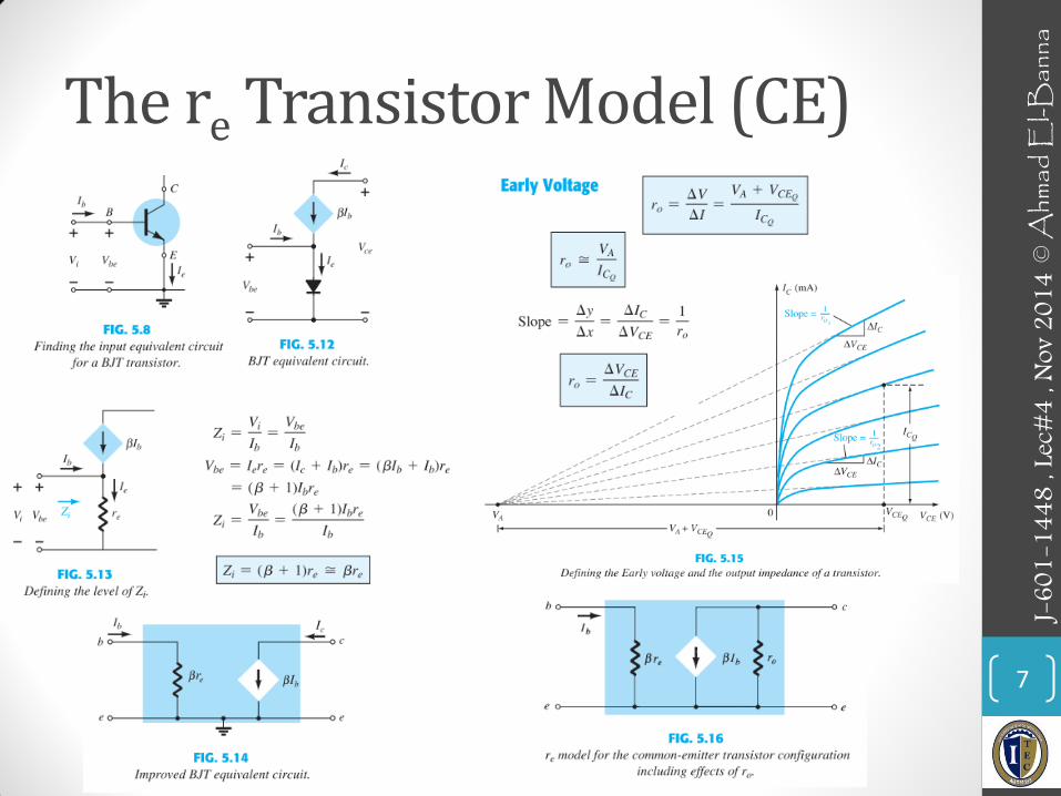
The re Transistor Model (CE)
7
J-601
-144
8 , L
ec#4
, Nov
201
4 ©
Ahm
ad E
l-Ban
na

The re Transistor Model (CB)
8
J-601
-144
8 , L
ec#4
, Nov
201
4 ©
Ahm
ad E
l-Ban
na

The re Transistor Model (CC)
9
• For the common-collector configuration, the model defined for the common-emitter configuration of is normally applied rather than defining a model for the common-collector configuration.
• The dc analysis of npn and pnp configurations is quite different in the sense that the currents will have opposite directions and the voltages opposite polarities.
• However, for an ac analysis where the signal will progress between positive and negative values, the ac equivalent circuit will be the same.
npn versus pnp
J-601
-144
8 , L
ec#4
, Nov
201
4 ©
Ahm
ad E
l-Ban
na

C.E. Fixed Bias Configuration
10
J-601
-144
8 , L
ec#4
, Nov
201
4 ©
Ahm
ad E
l-Ban
na
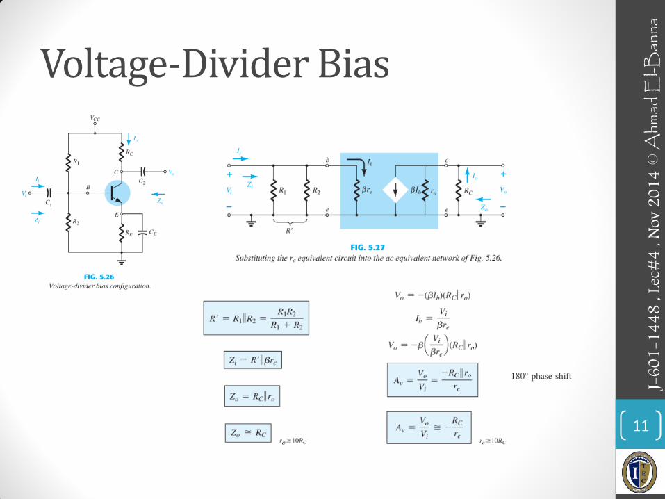
Voltage-Divider Bias
11
J-601
-144
8 , L
ec#4
, Nov
201
4 ©
Ahm
ad E
l-Ban
na

EFFECT OF RL AND RS
(SYSTEM APPROACH)
12
J-601
-144
8 , L
ec#4
, Nov
201
4 ©
Ahm
ad E
l-Ban
na

Effect of RL and Rs
13
• The loaded voltage gain of an amplifier is always less than the no-load gain. • The gain obtained with a source resistance in place will always be less than that obtained under
loaded or unloaded conditions due to the drop in applied voltage across the source resistance. • For the same configuration AvNL>AvL> Avs. • For a particular design, the larger the level of R L , the greater is the level of ac gain. • For a particular amplifier, the smaller the internal resistance of the signal source, the greater is
the overall gain. • For any network that have coupling capacitors, the source and load resistance do not affect the dc
biasing levels.
J-601
-144
8 , L
ec#4
, Nov
201
4 ©
Ahm
ad E
l-Ban
na

Effect of RL and Rs ..
14
Voltage-divider ct.
J-601
-144
8 , L
ec#4
, Nov
201
4 ©
Ahm
ad E
l-Ban
na

DETERMINING THE CURRENT GAIN 15
J-601
-144
8 , L
ec#4
, Nov
201
4 ©
Ahm
ad E
l-Ban
na
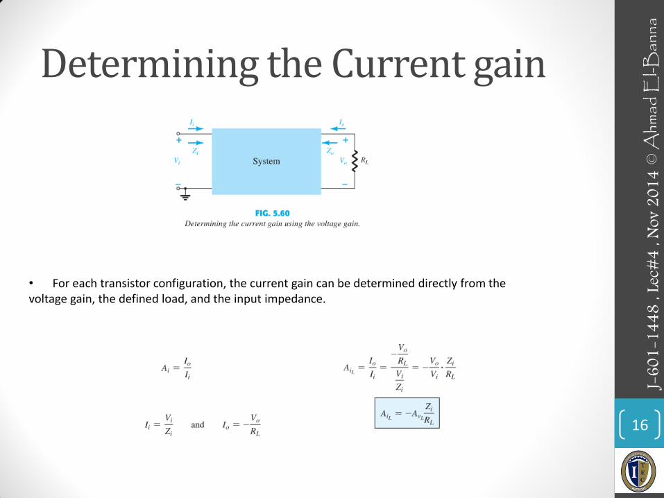
Determining the Current gain
16
• For each transistor configuration, the current gain can be determined directly from the voltage gain, the defined load, and the input impedance.
J-601
-144
8 , L
ec#4
, Nov
201
4 ©
Ahm
ad E
l-Ban
na

SUMMARY TABLE 17
J-601
-144
8 , L
ec#4
, Nov
201
4 ©
Ahm
ad E
l-Ban
na

18
J-601
-144
8 , L
ec#4
, Nov
201
4 ©
Ahm
ad E
l-Ban
na

19
J-601
-144
8 , L
ec#4
, Nov
201
4 ©
Ahm
ad E
l-Ban
na

20
J-601
-144
8 , L
ec#4
, Nov
201
4 ©
Ahm
ad E
l-Ban
na

TWO PORT SYSTEMS APPROACH 21
© A
hmad
El-B
anna
J-6
01-1
448
, Lec
#4 , N
ov 2
014

2-Port System
22
© A
hmad
El-B
anna
J-6
01-1
448
, Lec
#4 , N
ov 2
014

2-Port System..
23
© A
hmad
El-B
anna
J-6
01-1
448
, Lec
#4 , N
ov 2
014

CASCADED SYSTEMS 24
© A
hmad
El-B
anna
J-6
01-1
448
, Lec
#4 , N
ov 2
014
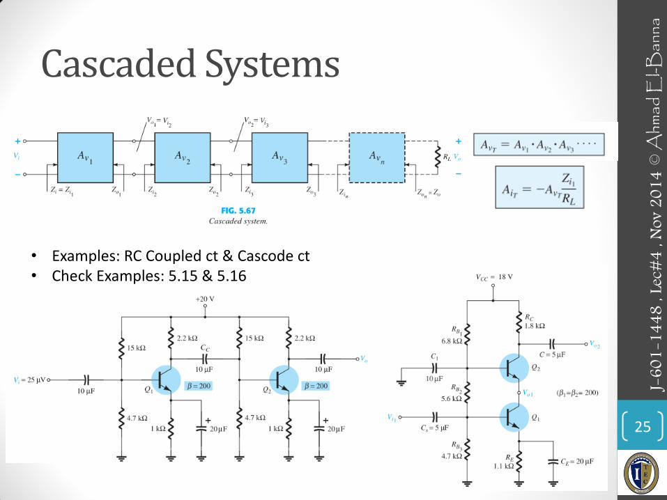
Cascaded Systems
25
© A
hmad
El-B
anna
• Examples: RC Coupled ct & Cascode ct • Check Examples: 5.15 & 5.16
J-601
-144
8 , L
ec#4
, Nov
201
4

THE HYBRID EQUIVALENT MODEL 26
© A
hmad
El-B
anna
J-6
01-1
448
, Lec
#4 , N
ov 2
014
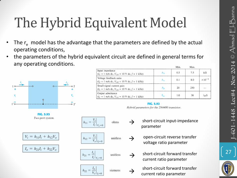
The Hybrid Equivalent Model
27
© A
hmad
El-B
anna
• The re model has the advantage that the parameters are defined by the actual operating conditions,
• the parameters of the hybrid equivalent circuit are defined in general terms for any operating conditions.
short-circuit forward transfer current ratio parameter
short-circuit forward transfer current ratio parameter
open-circuit reverse transfer voltage ratio parameter
short-circuit input-impedance parameter
J-601
-144
8 , L
ec#4
, Nov
201
4

Transistor Hybrid Equivalent ct
28
© A
hmad
El-B
anna
• For Transistor:
J-601
-144
8 , L
ec#4
, Nov
201
4

Hybrid vs. re model
29
© A
hmad
El-B
anna
J-6
01-1
448
, Lec
#4 , N
ov 2
014

APPROXIMATE & COMPLETE H-MODEL 30
© A
hmad
El-B
anna
J-6
01-1
448
, Lec
#4 , N
ov 2
014

Approximate h-model
31
© A
hmad
El-B
anna
• Fixed Bias ct
• Check other configurations !!
J-601
-144
8 , L
ec#4
, Nov
201
4
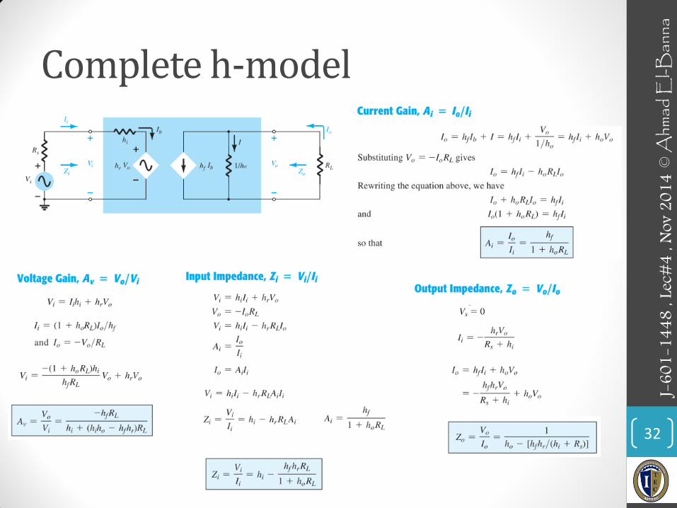
Complete h-model
32
© A
hmad
El-B
anna
J-6
01-1
448
, Lec
#4 , N
ov 2
014

HYBRID Π MODEL 33
© A
hmad
El-B
anna
J-6
01-1
448
, Lec
#4 , N
ov 2
014
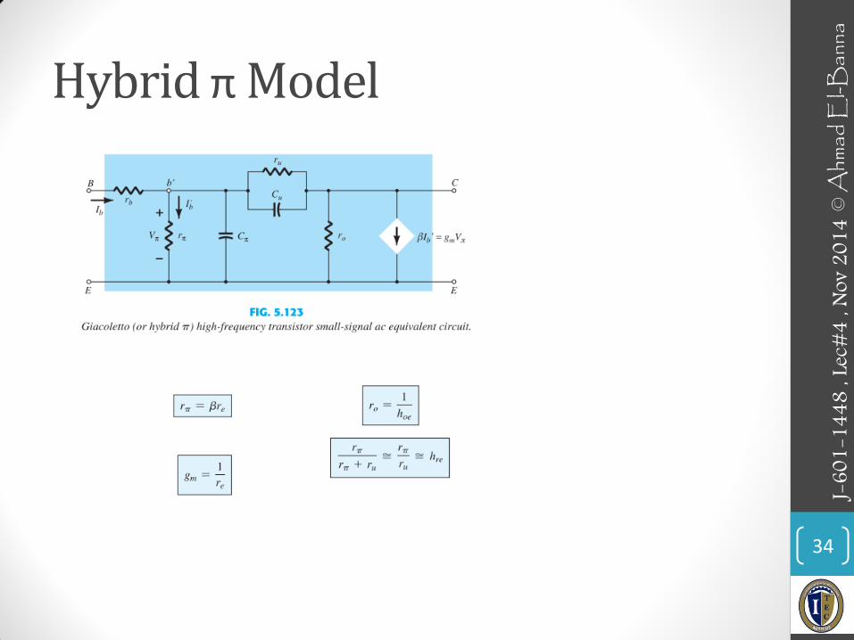
Hybrid π Model
34
© A
hmad
El-B
anna
J-6
01-1
448
, Lec
#4 , N
ov 2
014

VARIATIONS OF TRANSISTOR PARAMETERS
35
© A
hmad
El-B
anna
J-6
01-1
448
, Lec
#4 , N
ov 2
014

TROUBLESHOOTING & PRACTICAL APPLICATIONS
36
© A
hmad
El-B
anna
J-6
01-1
448
, Lec
#4 , N
ov 2
014

Troubleshooting
37
© A
hmad
El-B
anna
J-6
01-1
448
, Lec
#4 , N
ov 2
014
In general, therefore, if a system is not working properly, first disconnect the ac source and check the dc biasing levels.

PRACTICAL APPLICATIONS
38
© A
hmad
El-B
anna
J-6
01-1
448
, Lec
#4 , N
ov 2
014
• Audio Mixer
• Preamplifier

• For more details, refer to:
• Chapter 5, Electronic Devices and Circuits, Boylestad.
• The lecture is available online at:
• https://speakerdeck.com/ahmad_elbanna
• For inquires, send to:
39
J-601
-144
8 , L
ec#4
, Nov
201
4 ©
Ahm
ad E
l-Ban
na