lecture 16 current mirrors and simple referencesa current mirror replicates the input current of a...
TRANSCRIPT
Lecture 16 – Current Mirrors and Simple References (6/14/14) Page 16-1
CMOS Analog Circuit Design © P.E. Allen - 2016
LECTURE 16 – CURRENT MIRRORS AND SIMPLE
REFERENCES
LECTURE ORGANIZATION
Outline
• MOSFET current mirrors
• Improved current mirrors
• Voltage references with power supply independence
• Current references with power supply independence
• Temperature behavior of voltage and current references
CMOS Analog Circuit Design, 3rd Edition Reference
Pages 138-156
Lecture 16 – Current Mirrors and Simple References (6/14/14) Page 16-2
CMOS Analog Circuit Design © P.E. Allen - 2016
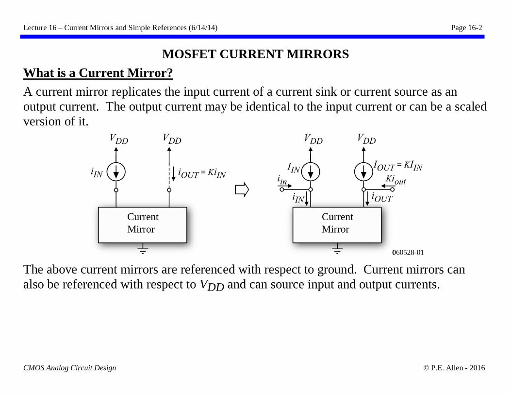
MOSFET CURRENT MIRRORS
What is a Current Mirror?
A current mirror replicates the input current of a current sink or current source as an
output current. The output current may be identical to the input current or can be a scaled
version of it.
The above current mirrors are referenced with respect to ground. Current mirrors can
also be referenced with respect to VDD and can source input and output currents.
060528-01
VDD
Current
Mirror
iIN
VDD
iOUT = KiIN
VDD
Current
Mirror
IIN
VDD
IOUT = KIIN
iin Kiout
iOUTiIN
Lecture 16 – Current Mirrors and Simple References (6/14/14) Page 16-3
CMOS Analog Circuit Design © P.E. Allen - 2016
Characterization of Current Mirrors
A current mirror is basically nothing more than a current amplifier. The ideal
characteristics of a current amplifier are:
• Output current linearly related to the input current, iout = Aiiin
• Input resistance is zero
• Output resistance is infinity
Also, the characteristic VMIN applies not only to the output but also the input.
• VMIN(in) is the range of vin over which the input resistance is not small
• VMIN(out) is the range of vout over which the output resistance is not large
Graphically:
Therefore, Rout, Rin, VMIN(out), VMIN(in), and Ai will characterize the current mirror.
Lecture 16 – Current Mirrors and Simple References (6/14/14) Page 16-4
CMOS Analog Circuit Design © P.E. Allen - 2016
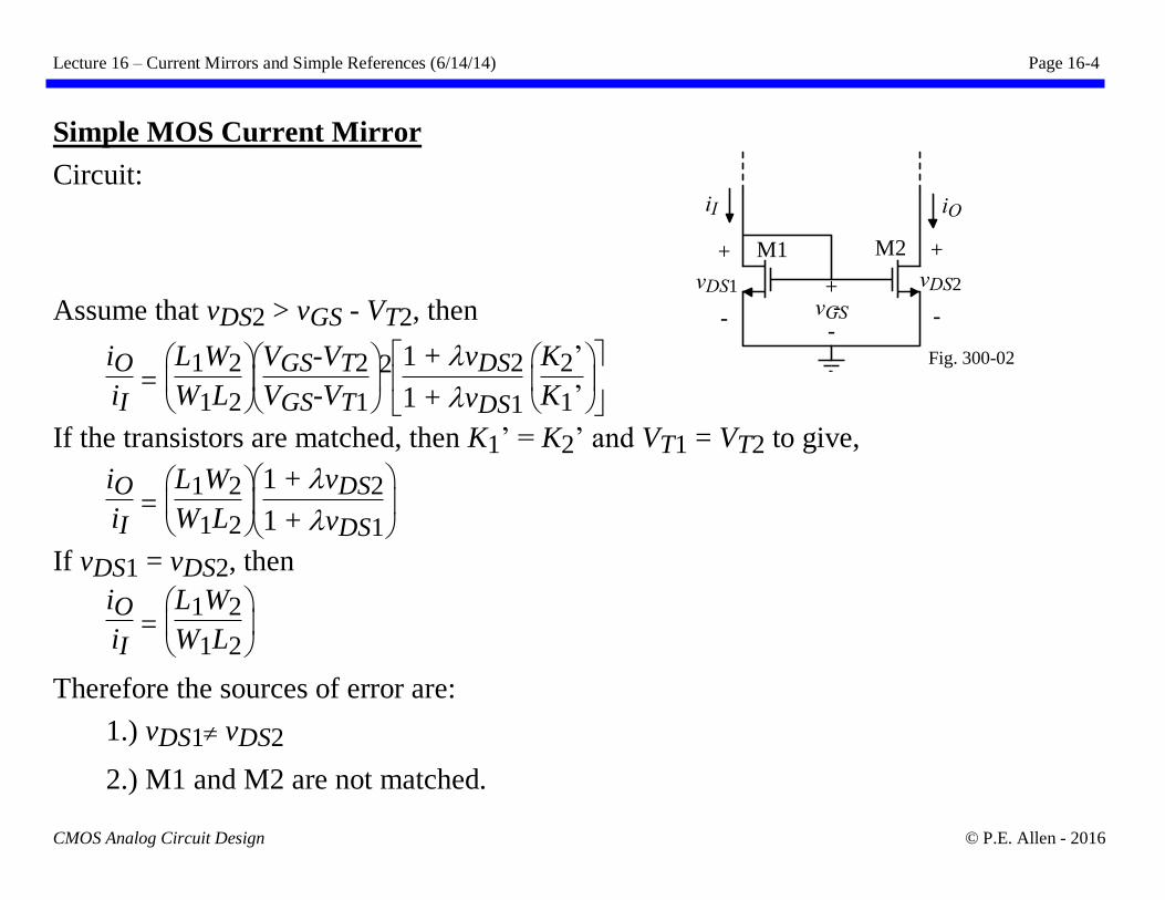
Simple MOS Current Mirror
Circuit:
Assume that vDS2 > vGS - VT2, then
iOiI
=
L1W2
W1L2
VGS-VT2
VGS-VT1
2
1 + vDS2
1 + vDS1
K2’
K1’
If the transistors are matched, then K1’ = K2’ and VT1 = VT2 to give,
iO
iI =
L1W2
W1L2
1 + vDS2
1 + vDS1
If vDS1 = vDS2, then
iOiI
=
L1W2
W1L2
Therefore the sources of error are:
1.) vDS1 vDS2
2.) M1 and M2 are not matched.
M1 M2
iI iO
+
-
vDS1
+
-
vDS2
Fig. 300-02
+-vGS-
Lecture 16 – Current Mirrors and Simple References (6/14/14) Page 16-5
CMOS Analog Circuit Design © P.E. Allen - 2016
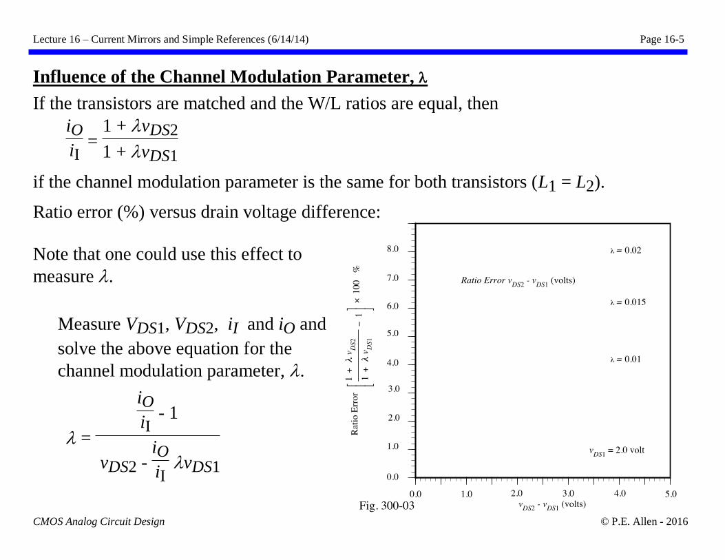
Influence of the Channel Modulation Parameter,
If the transistors are matched and the W/L ratios are equal, then
iO
iI =
1 + vDS2
1 + vDS1
if the channel modulation parameter is the same for both transistors (L1 = L2).
Ratio error (%) versus drain voltage difference:
Note that one could use this effect to
measure .
Measure VDS1, VDS2, iI and iO and
solve the above equation for the
channel modulation parameter, .
=
iO
iI - 1
vDS2 - iOiI
vDS1
Lecture 16 – Current Mirrors and Simple References (6/14/14) Page 16-6
CMOS Analog Circuit Design © P.E. Allen - 2016
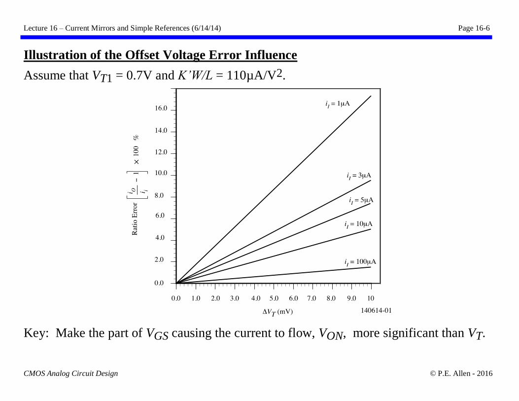
Illustration of the Offset Voltage Error Influence
Assume that VT1 = 0.7V and K’W/L = 110µA/V2.
Key: Make the part of VGS causing the current to flow, VON, more significant than VT.
Lecture 16 – Current Mirrors and Simple References (6/14/14) Page 16-7
CMOS Analog Circuit Design © P.E. Allen - 2016
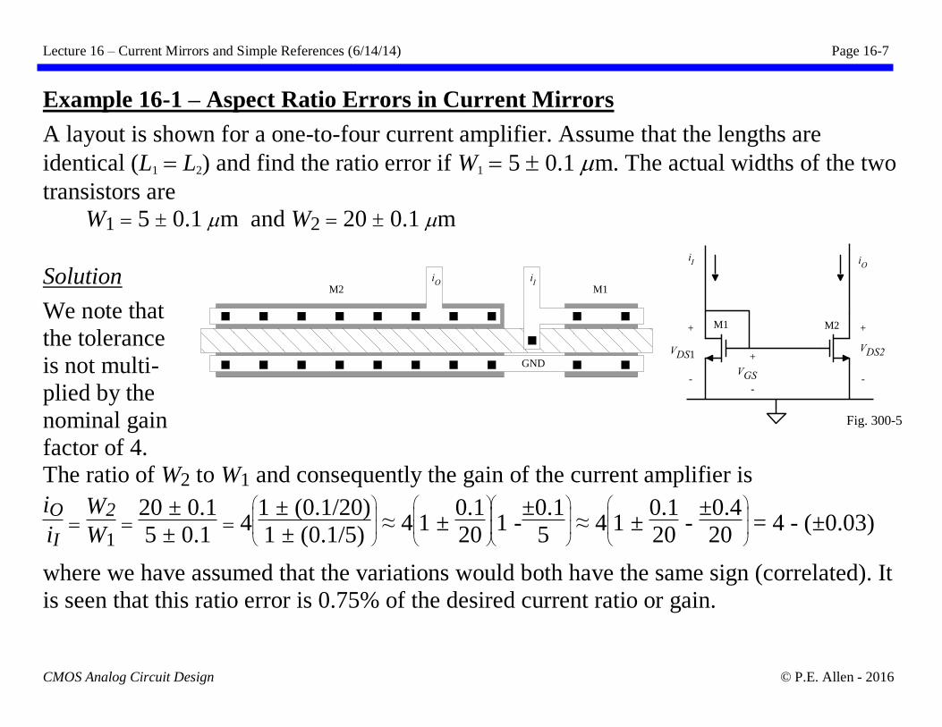
Example 16-1 – Aspect Ratio Errors in Current Mirrors
A layout is shown for a one-to-four current amplifier. Assume that the lengths are
identical (L1 = L2) and find the ratio error if W1 = 5 0.1 m. The actual widths of the two
transistors are
W1 = 5 0.1 m and W2 = 20 0.1 m
Solution
We note that
the tolerance
is not multi-
plied by the
nominal gain
factor of 4.
The ratio of W2 to W1 and consequently the gain of the current amplifier is
iOiI
= W2
W1 =
20 ± 0.1
5 ± 0.1 = 4
1 ± (0.1/20)
1 ± (0.1/5) ≈ 4
1 ± 0.1
20
1 -±0.1
5 ≈ 4
1 ± 0.1
20 -
±0.4
20 = 4 - (±0.03)
where we have assumed that the variations would both have the same sign (correlated). It
is seen that this ratio error is 0.75% of the desired current ratio or gain.
iO
M1 M2
+
-
+
-
+
-
VDS1VDS2
iI
VGS
M1M2iO
iI
GND
Fig. 300-5
Lecture 16 – Current Mirrors and Simple References (6/14/14) Page 16-8
CMOS Analog Circuit Design © P.E. Allen - 2016
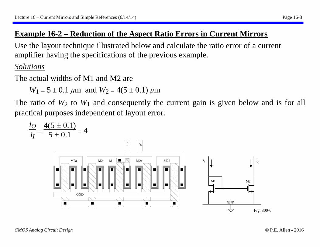
Example 16-2 – Reduction of the Aspect Ratio Errors in Current Mirrors
Use the layout technique illustrated below and calculate the ratio error of a current
amplifier having the specifications of the previous example.
Solutions
The actual widths of M1 and M2 are
W1 = 5 0.1 m and W2 = 4(5 0.1) m
The ratio of W2 to W1 and consequently the current gain is given below and is for all
practical purposes independent of layout error.
iOiI
= 4(5 ± 0.1)
5 ± 0.1 = 4
M1M2bM2a M2dM2c iO
M1 M2
iI
iI
GND
GND
iO
Fig. 300-6
Lecture 16 – Current Mirrors and Simple References (6/14/14) Page 16-9
CMOS Analog Circuit Design © P.E. Allen - 2016
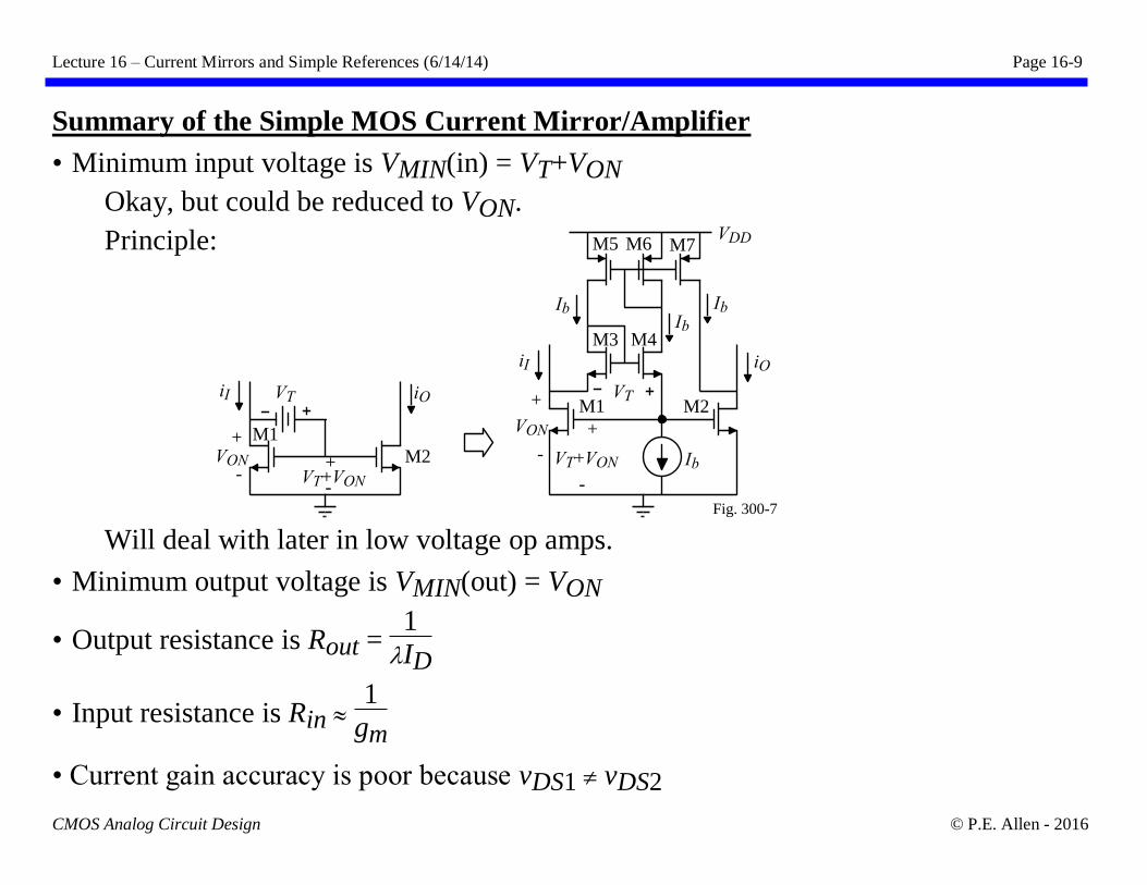
Summary of the Simple MOS Current Mirror/Amplifier
• Minimum input voltage is VMIN(in) = VT+VON
Okay, but could be reduced to VON.
Principle:
Will deal with later in low voltage op amps.
• Minimum output voltage is VMIN(out) = VON
• Output resistance is Rout = 1
ID
• Input resistance is Rin 1
gm
• Current gain accuracy is poor because vDS1 vDS2
M1
M2
VTiI iO
VT+VON
+
-
+
-VON
M1 M2VT
Fig. 300-7
iI iO
VT+VON
+
-
+
-
VON
Ib
IbIb
VDD
Ib
M3 M4
M5 M6 M7
Lecture 16 – Current Mirrors and Simple References (6/14/14) Page 16-10
CMOS Analog Circuit Design © P.E. Allen - 2016
IMPROVED CURRENT MIRRORS
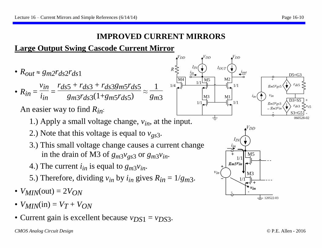
Large Output Swing Cascode Current Mirror
• Rout gm2rds2rds1
• Rin = vin
iin =
rds5 + rds3 + rds3gm5rds5
gm3rds3(1+gm5rds5) ≈
1
gm3
An easier way to find Rin:
1.) Apply a small voltage change, vin, at the input.
2.) Note that this voltage is equal to vgs3.
3.) This small voltage change causes a current change
in the drain of M3 of gm3vgs3 or gm3vin.
4.) The current iin is equal to gm3vin.
5.) Therefore, dividing vin by iin gives Rin = 1/gm3.
• VMIN(out) = 2VON
• VMIN(in) = VT + VON
• Current gain is excellent because vDS1 = vDS3.
060528-02
M2
M1M3
1/4
M4
VDD
IIN IOUT
M5
iin
1/1
1/1
1/1
1/1
gm5vgs5rds5
gm3vgs3 rds3
+
-
vs5
D5=G3
D3=S5
S3=G5
+
-
viniin
= gm3vin
VDD VDD
ioutR
M3
IIN
M5
iin
1/1
1/1
VDD
+
-
vin
vin
+
-
gm3vin
120522-03
Lecture 16 – Current Mirrors and Simple References (6/14/14) Page 16-11
CMOS Analog Circuit Design © P.E. Allen - 2016
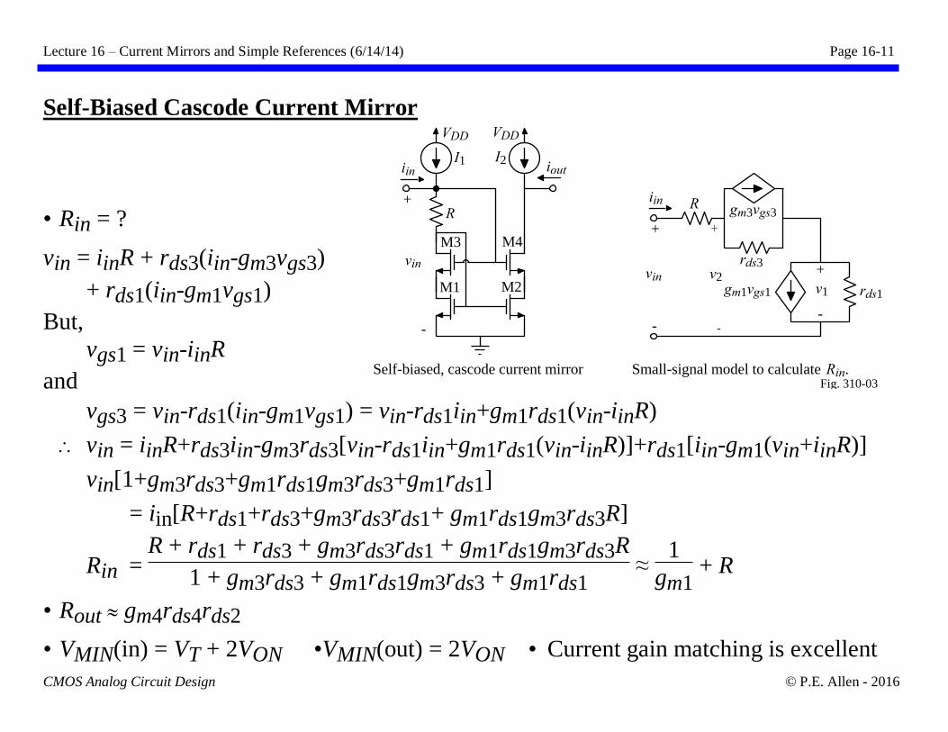
Self-Biased Cascode Current Mirror
• Rin = ?
vin = iinR + rds3(iin-gm3vgs3)
+ rds1(iin-gm1vgs1)
But,
vgs1 = vin-iinR
and
vgs3 = vin-rds1(iin-gm1vgs1) = vin-rds1iin+gm1rds1(vin-iinR)
vin = iinR+rds3iin-gm3rds3[vin-rds1iin+gm1rds1(vin-iinR)]+rds1[iin-gm1(vin+iinR)]
vin[1+gm3rds3+gm1rds1gm3rds3+gm1rds1]
= iin[R+rds1+rds3+gm3rds3rds1+ gm1rds1gm3rds3R]
Rin =
R + rds1 + rds3 + gm3rds3rds1 + gm1rds1gm3rds3R
1 + gm3rds3 + gm1rds1gm3rds3 + gm1rds1 ≈
1
gm1 + R
• Rout gm4rds4rds2
• VMIN(in) = VT + 2VON •VMIN(out) = 2VON • Current gain matching is excellent
VDD VDD
I1 I2iin iout
R
M1 M2
M3 M4
gm3vgs3
rds3
R
gm1vgs1 rds1
+
-
vin
+
-
v2v1
+
-
+
-
vin
Small-signal model to calculate Rin.Self-biased, cascode current mirrorFig. 310-03
iin
Lecture 16 – Current Mirrors and Simple References (6/14/14) Page 16-12
CMOS Analog Circuit Design © P.E. Allen - 2016
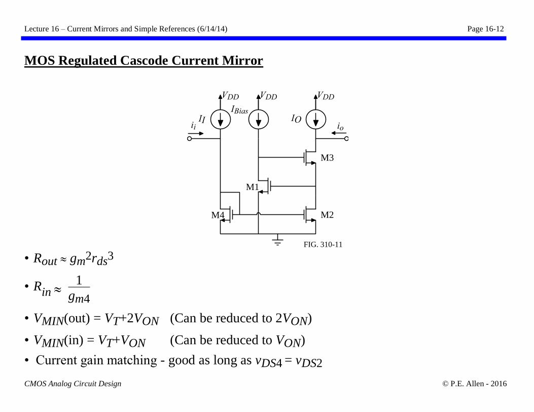
MOS Regulated Cascode Current Mirror
• Rout gm2rds3
• Rin 1
gm4
• VMIN(out) = VT+2VON (Can be reduced to 2VON)
• VMIN(in) = VT+VON (Can be reduced to VON)
• Current gain matching - good as long as vDS4 = vDS2
IBiasIO
M3
M2
M1
ii
M4
FIG. 310-11
VDD
io
VDD
II
VDD
Lecture 16 – Current Mirrors and Simple References (6/14/14) Page 16-13
CMOS Analog Circuit Design © P.E. Allen - 2016
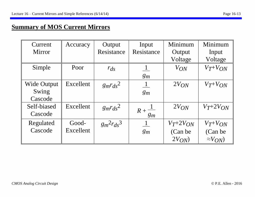
Summary of MOS Current Mirrors
Current
Mirror
Accuracy Output
Resistance
Input
Resistance
Minimum
Output
Voltage
Minimum
Input
Voltage
Simple Poor rds 1
gm
VON VT+VON
Wide Output
Swing
Cascode
Excellent gmrds2 1
gm
2VON VT+VON
Self-biased
Cascode
Excellent gmrds2 R +
1
gm
2VON VT+2VON
Regulated
Cascode
Good-
Excellent gm2rds3 1
gm
VT+2VON
(Can be
2VON)
VT+VON
(Can be
≈VON)
Lecture 16 – Current Mirrors and Simple References (6/14/14) Page 16-14
CMOS Analog Circuit Design © P.E. Allen - 2016
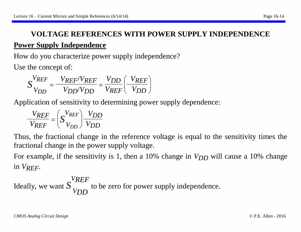
VOLTAGE REFERENCES WITH POWER SUPPLY INDEPENDENCE
Power Supply Independence
How do you characterize power supply independence?
Use the concept of:
SVREF
VDD =
VREF/VREF
VDD/VDD =
VDD
VREF
VREF
VDD
Application of sensitivity to determining power supply dependence:
VREF
VREF =
SVREF
VDD
VDD
VDD
Thus, the fractional change in the reference voltage is equal to the sensitivity times the
fractional change in the power supply voltage.
For example, if the sensitivity is 1, then a 10% change in VDD will cause a 10% change
in VREF.
Ideally, we want SVREF
VDD to be zero for power supply independence.
Lecture 16 – Current Mirrors and Simple References (6/14/14) Page 16-15
CMOS Analog Circuit Design © P.E. Allen - 2016
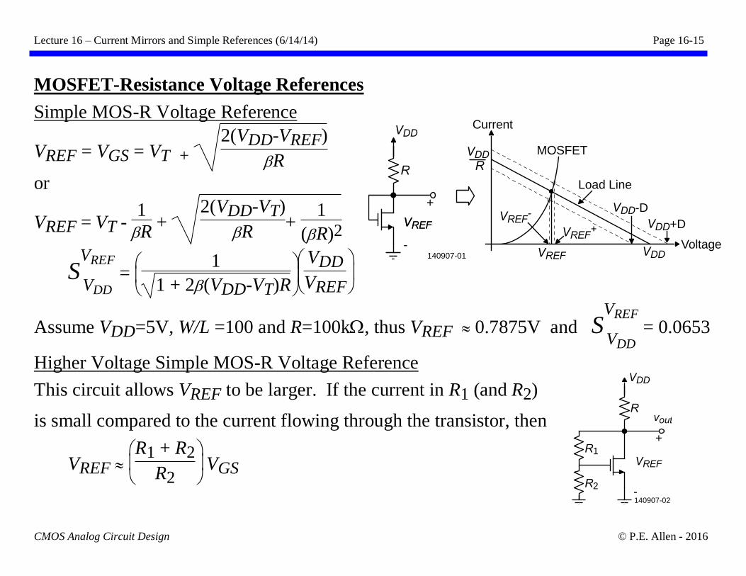
MOSFET-Resistance Voltage References
Simple MOS-R Voltage Reference
VREF = VGS = VT +
2(VDD-VREF)
R
or
VREF = VT - 1
R +
2(VDD-VT)
R+
1
(R)2
SVREF
VDD
=
1
1 + 2(VDD-VT)R
VDD
VREF
Assume VDD=5V, W/L =100 and R=100k, thus VREF 0.7875V and SVREF
VDD
= 0.0653
Higher Voltage Simple MOS-R Voltage Reference
This circuit allows VREF to be larger. If the current in R1 (and R2)
is small compared to the current flowing through the transistor, then
VREF
R1 + R2
R2 VGS
vout
VDD
+
-
R
VREF
R1
R2
140907-02
VDD
+
-
R
VREF
VDD
VDDR
MOSFET
Load Line
VDD+D
VDD-D
VREF
VREFVREF
+
VREF-
Voltage
Current
140907-01
Lecture 16 – Current Mirrors and Simple References (6/14/14) Page 16-16
CMOS Analog Circuit Design © P.E. Allen - 2016
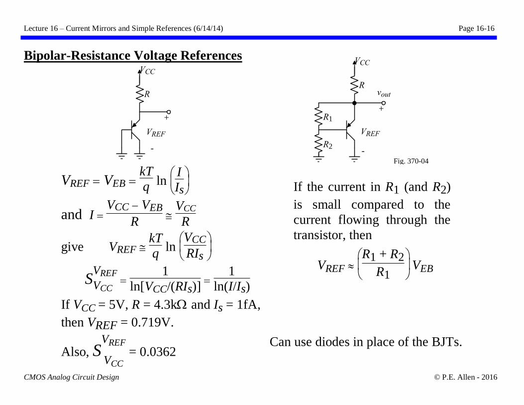
Bipolar-Resistance Voltage References
VREF = VEB = kT
q ln
I
Is
and I = VCC − VEB
R
VCC
R
give VREF kT
q ln
VCC
RIs
SVREF
VCC =
1
ln[VCC/(RIs)] =
1
ln(I/Is)
If VCC = 5V, R = 4.3k and Is = 1fA,
then VREF = 0.719V.
Also, SVREF
VCC
= 0.0362
If the current in R1 (and R2)
is small compared to the
current flowing through the
transistor, then
VREF
R1 + R2
R1 VEB
Can use diodes in place of the BJTs.
vout
VCC
+
-
R
VREF
VCC
+
-
R
VREF
R1
R2
Fig. 370-04
Lecture 16 – Current Mirrors and Simple References (6/14/14) Page 16-17
CMOS Analog Circuit Design © P.E. Allen - 2016
CURRENT REFERENCES WITH POWER SUPPLY INDEPENDENCE
Power Supply Independence
Again, we want
SIREF
VDD =
IREF/IREF
VDD/VDD =
VDD
IREF
IREF
VDD
to approach zero.
Therefore, as SIREF
VDD approaches zero, the change in IREF as a function of a change in
VDD approaches zero.
Lecture 16 – Current Mirrors and Simple References (6/14/14) Page 16-18
CMOS Analog Circuit Design © P.E. Allen - 2016
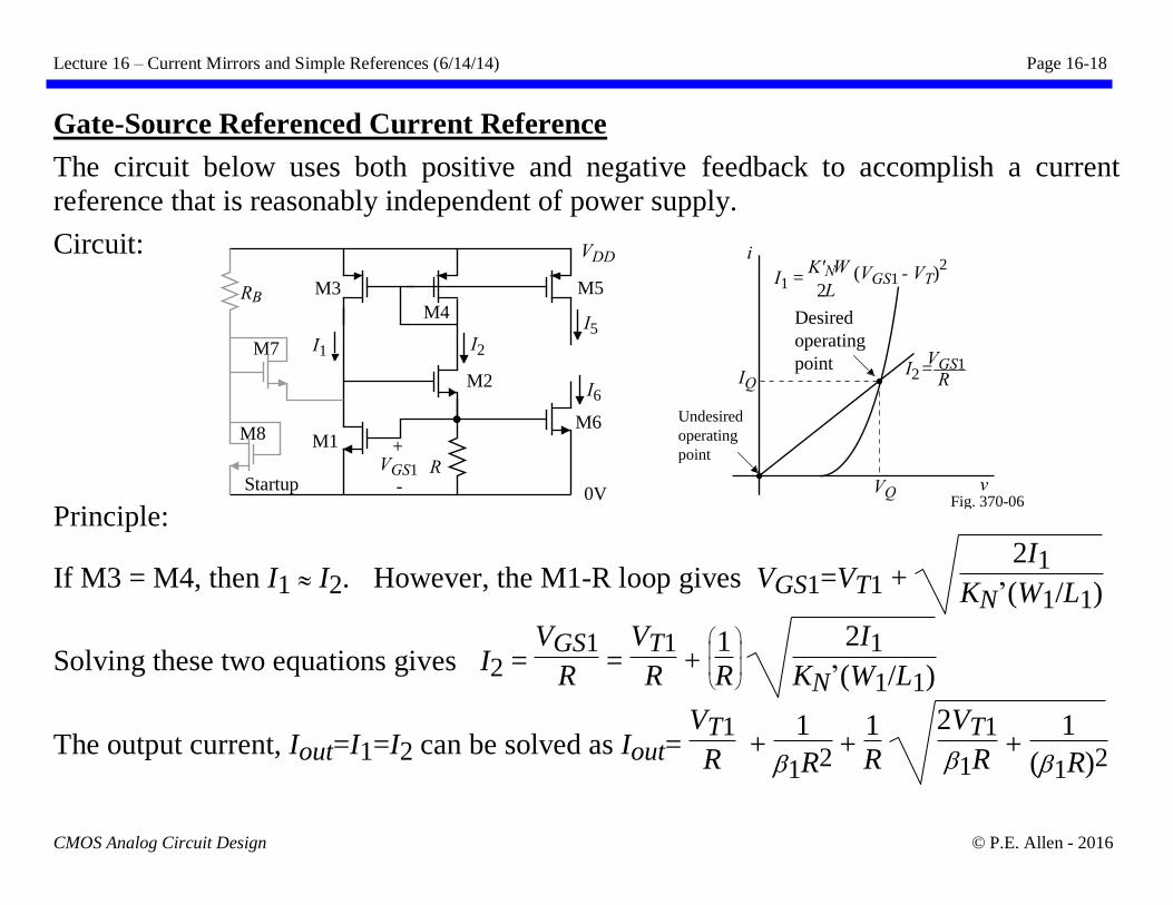
Gate-Source Referenced Current Reference
The circuit below uses both positive and negative feedback to accomplish a current
reference that is reasonably independent of power supply.
Circuit:
Principle:
If M3 = M4, then I1 I2. However, the M1-R loop gives VGS1=VT1 + 2I1
KN’(W1/L1)
Solving these two equations gives I2 = VGS1
R =
VT1
R +
1
R
2I1
KN’(W1/L1)
The output current, Iout=I1=I2 can be solved as Iout= VT1
R +
1
1R2 +
1
R
2VT1
1R +
1
(1R)2
i
v
IQ
VQ
RI2
=
W
LI1 =
(VGS1 - VT)2
M2
+
-
M1
I5
M8
VGS1
M3
M4
R
I6
M5
M6
I1 I2
Startup
VDD
VGS1M7
Fig. 370-06
Desired
operating
point
Undesired
operating
point
0V
K'N2RB
Lecture 16 – Current Mirrors and Simple References (6/14/14) Page 16-19
CMOS Analog Circuit Design © P.E. Allen - 2016
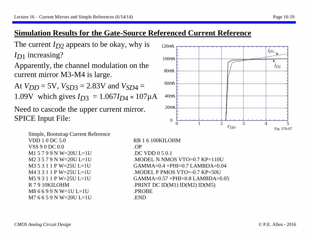
Simulation Results for the Gate-Source Referenced Current Reference
The current ID2 appears to be okay, why is
ID1 increasing?
Apparently, the channel modulation on the
current mirror M3-M4 is large.
At VDD = 5V, VSD3 = 2.83V and VSD4 =
1.09V which gives ID3 = 1.067ID4 107µA
Need to cascode the upper current mirror.
SPICE Input File:
Simple, Bootstrap Current Reference
VDD 1 0 DC 5.0
VSS 9 0 DC 0.0
M1 5 7 9 9 N W=20U L=1U
M2 3 5 7 9 N W=20U L=1U
M3 5 3 1 1 P W=25U L=1U
M4 3 3 1 1 P W=25U L=1U
M5 9 3 1 1 P W=25U L=1U
R 7 9 10KILOHM
M8 6 6 9 9 N W=1U L=1U
M7 6 6 5 9 N W=20U L=1U
RB 1 6 100KILOHM
.OP
.DC VDD 0 5 0.1
.MODEL N NMOS VTO=0.7 KP=110U
GAMMA=0.4 +PHI=0.7 LAMBDA=0.04
.MODEL P PMOS VTO=-0.7 KP=50U
GAMMA=0.57 +PHI=0.8 LAMBDA=0.05
.PRINT DC ID(M1) ID(M2) ID(M5)
.PROBE
.END
0 1 2 3 4 5VDD
120mA
100mA
80mA
60mA
40mA
20mA
0
ID1
ID2
Fig. 370-07
Lecture 16 – Current Mirrors and Simple References (6/14/14) Page 16-20
CMOS Analog Circuit Design © P.E. Allen - 2016
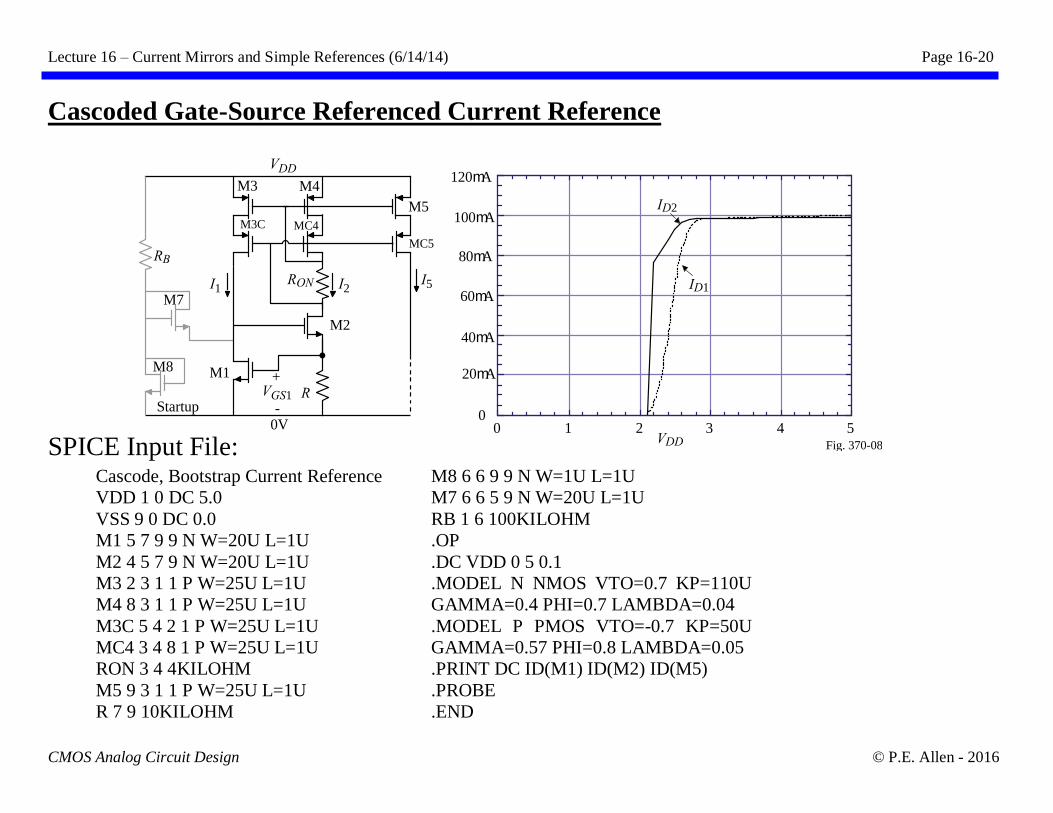
Cascoded Gate-Source Referenced Current Reference
SPICE Input File: Cascode, Bootstrap Current Reference
VDD 1 0 DC 5.0
VSS 9 0 DC 0.0
M1 5 7 9 9 N W=20U L=1U
M2 4 5 7 9 N W=20U L=1U
M3 2 3 1 1 P W=25U L=1U
M4 8 3 1 1 P W=25U L=1U
M3C 5 4 2 1 P W=25U L=1U
MC4 3 4 8 1 P W=25U L=1U
RON 3 4 4KILOHM
M5 9 3 1 1 P W=25U L=1U
R 7 9 10KILOHM
M8 6 6 9 9 N W=1U L=1U
M7 6 6 5 9 N W=20U L=1U
RB 1 6 100KILOHM
.OP
.DC VDD 0 5 0.1
.MODEL N NMOS VTO=0.7 KP=110U
GAMMA=0.4 PHI=0.7 LAMBDA=0.04
.MODEL P PMOS VTO=-0.7 KP=50U
GAMMA=0.57 PHI=0.8 LAMBDA=0.05
.PRINT DC ID(M1) ID(M2) ID(M5)
.PROBE
.END
0 1 2 3 4 5VDD
120mA
100mA
80mA
60mA
40mA
20mA
0
ID1
ID2
Fig. 370-08
M2
+
-
M1
I5
M8
VGS1
M3 M4
R
M5
I1 I2
Startup
VDD
M7
0V
RB
M3C MC4
MC5
RON
Lecture 16 – Current Mirrors and Simple References (6/14/14) Page 16-21
CMOS Analog Circuit Design © P.E. Allen - 2016
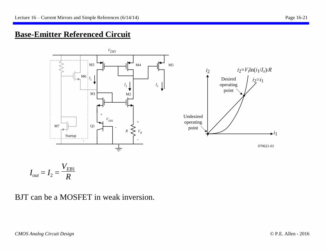
Base-Emitter Referenced Circuit
Iout = I2 = VEB1
R
BJT can be a MOSFET in weak inversion.
M2
+
-
+
-
M1
I5
M7
-
VEB1
VR
M3 M4
R
M5
I1
I2
Startup
Q1
VDD
070621-01
i2
i1
Desired
operating
point
Undesired
operating
point
i2=Vtln(i1/Is)/R
i2=i1M6
Lecture 16 – Current Mirrors and Simple References (6/14/14) Page 16-22
CMOS Analog Circuit Design © P.E. Allen - 2016
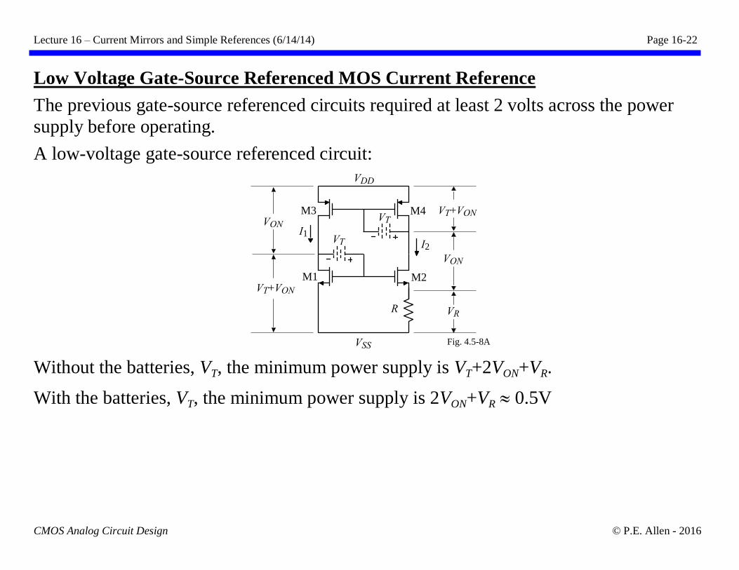
Low Voltage Gate-Source Referenced MOS Current Reference
The previous gate-source referenced circuits required at least 2 volts across the power
supply before operating.
A low-voltage gate-source referenced circuit:
Without the batteries, VT, the minimum power supply is VT+2VON+VR.
With the batteries, VT, the minimum power supply is 2VON+VR 0.5V
VSS
M3 M4
VDD
R
M1 M2
VT
VT
I1
I2
VT+VON
VON
VR
VT+VON
VON
Fig. 4.5-8A
Lecture 16 – Current Mirrors and Simple References (6/14/14) Page 16-23
CMOS Analog Circuit Design © P.E. Allen - 2016
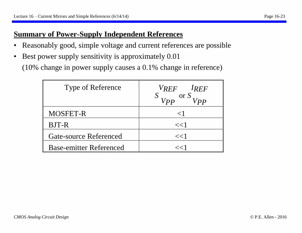
Summary of Power-Supply Independent References
• Reasonably good, simple voltage and current references are possible
• Best power supply sensitivity is approximately 0.01
(10% change in power supply causes a 0.1% change in reference)
Type of Reference SVREF
VPP or S
IREF
VPP
MOSFET-R <1
BJT-R <<1
Gate-source Referenced <<1
Base-emitter Referenced <<1
Lecture 16 – Current Mirrors and Simple References (6/14/14) Page 16-24
CMOS Analog Circuit Design © P.E. Allen - 2016
TEMPERATURE BEHAVIOR OF VOLTAGE AND CURRENT REFERENCES
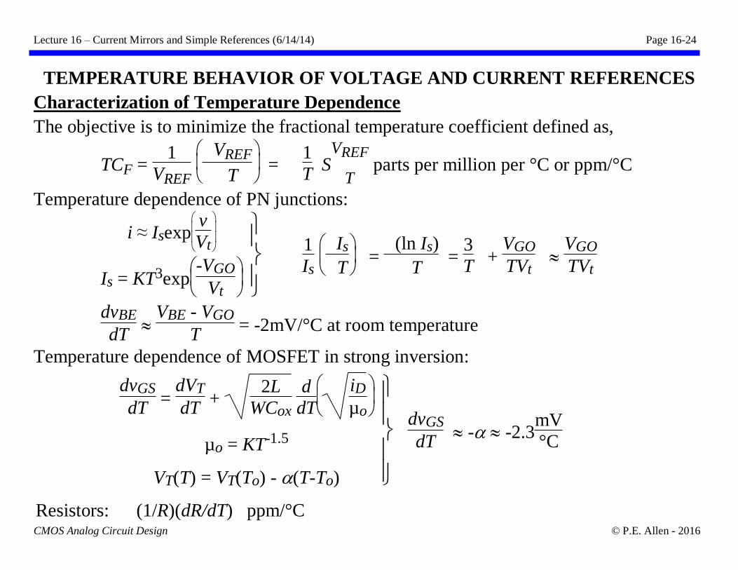
Characterization of Temperature Dependence
The objective is to minimize the fractional temperature coefficient defined as,
TCF = 1
VREF
VREF
T =
1
T S
VREF
T parts per million per °C or ppm/°C
Temperature dependence of PN junctions:
i ≈ Isexp
v
Vt
Is = KT3exp
-VGO
Vt
1
Is
Is
T =
(ln Is)
T =
3
T +
VGO
TVt
VGO
TVt
dvBE
dT
VBE - VGO
T = -2mV/°C at room temperature
Temperature dependence of MOSFET in strong inversion:
dvGS
dT =
dVT
dT +
2L
WCox
d
dT
iD
µo
µo = KT-1.5
VT(T) = VT(To) - (T-To)
dvGS
dT - -2.3
mV
°C
Resistors: (1/R)(dR/dT) ppm/°C
Lecture 16 – Current Mirrors and Simple References (6/14/14) Page 16-25
CMOS Analog Circuit Design © P.E. Allen - 2016
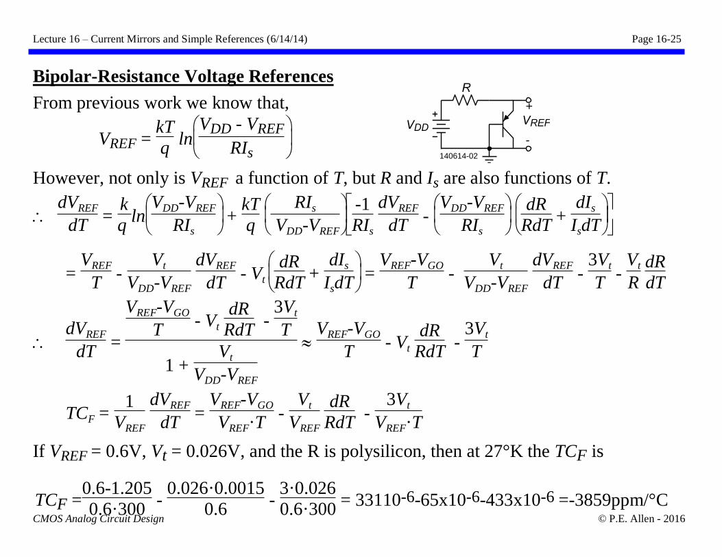
Bipolar-Resistance Voltage References
From previous work we know that,
VREF = kT
q ln
VDD - VREF
RIs
However, not only is VREF a function of T, but R and Is are also functions of T.
dVREF
dT =
k
q ln
VDD-VREF
RIs
+ kT
q
RIs
VDD-VREF
-1
RIs
dVREF
dT -
VDD-VREF
RIs
dR
RdT +
dIs
IsdT
= VREF
T -
Vt
VDD-VREF
dVREF
dT - Vt
dR
RdT +
dIs
IsdT =
VREF-VGO
T -
Vt
VDD-VREF
dVREF
dT -
3Vt
T -
Vt
R dR
dT
dVREF
dT =
VREF-VGO
T - Vt
dR
RdT -
3Vt
T
1 + Vt
VDD-VREF
VREF-VGO
T - Vt
dR
RdT -
3Vt
T
TCF = 1
VREF
dVREF
dT =
VREF-VGO
VREF·T -
Vt
VREF
dR
RdT -
3Vt
VREF·T
If VREF = 0.6V, Vt = 0.026V, and the R is polysilicon, then at 27°K the TCF is
TCF =0.6-1.205
0.6·300 -
0.026·0.0015
0.6 -
3·0.026
0.6·300 = 33110-6-65x10-6-433x10-6 =-3859ppm/°C
R
VDDVREF
+
-
140614-02
Lecture 16 – Current Mirrors and Simple References (6/14/14) Page 16-26
CMOS Analog Circuit Design © P.E. Allen - 2016
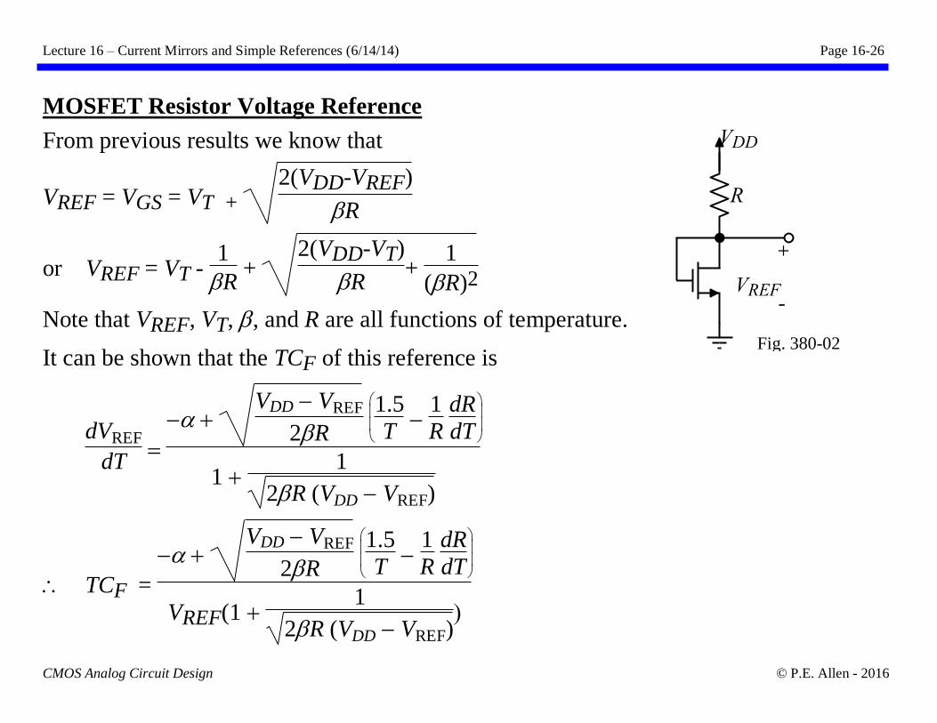
MOSFET Resistor Voltage Reference
From previous results we know that
VREF = VGS = VT +
2(VDD-VREF)
R
or VREF = VT - 1
R +
2(VDD-VT)
R+
1
(R)2
Note that VREF, VT, , and R are all functions of temperature.
It can be shown that the TCF of this reference is
dVREF
dT =
− + VDD − VREF
2R
1.5
T −
1
R dR
dT
1 + 1
2R (VDD − VREF)
TCF =
− + VDD − VREF
2R
1.5
T −
1
R dR
dT
VREF(1 + 1
2R (VDD − VREF))
VDD
+
-
R
VREF
Fig. 380-02
Lecture 16 – Current Mirrors and Simple References (6/14/14) Page 16-27
CMOS Analog Circuit Design © P.E. Allen - 2016
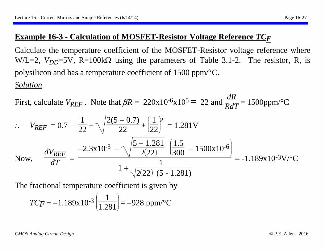
Example 16-3 - Calculation of MOSFET-Resistor Voltage Reference TCF
Calculate the temperature coefficient of the MOSFET-Resistor voltage reference where
W/L=2, VDD=5V, R=100k using the parameters of Table 3.1-2. The resistor, R, is
polysilicon and has a temperature coefficient of 1500 ppm/C.
Solution
First, calculate VREF . Note that R = 220x10-6x105 = 22 and dR
RdT = 1500ppm/°C
VREF = 0.7 − 1
22 +
2(5 − 0.7)
22 +
1
22
2 = 1.281V
Now, dVREF
dT =
−2.3x10⁻³ + 5 − 1.281
2
22
1.5
300 − 1500x10-6
1 + 1
2
22 (5 - 1.281)
= -1.189x10⁻³V/°C
The fractional temperature coefficient is given by
TCF = −1.189x10⁻³
1
1.281 = −928 ppm/°C
Lecture 16 – Current Mirrors and Simple References (6/14/14) Page 16-28
CMOS Analog Circuit Design © P.E. Allen - 2016
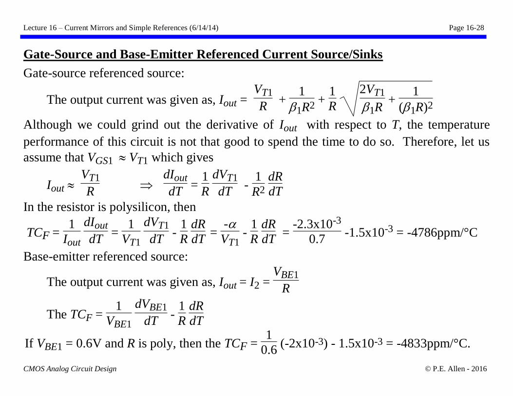
Gate-Source and Base-Emitter Referenced Current Source/Sinks
Gate-source referenced source:
The output current was given as, Iout = VT1
R +
1
1R2 +
1
R
2VT1
1R +
1
(1R)2
Although we could grind out the derivative of Iout with respect to T, the temperature
performance of this circuit is not that good to spend the time to do so. Therefore, let us
assume that VGS1 VT1 which gives
Iout VT1
R
dIout
dT =
1
R dVT1
dT -
1
R2 dR
dT
In the resistor is polysilicon, then
TCF = 1
Iout dIout
dT =
1
VT1 dVT1
dT -
1
R dR
dT =
-VT1
- 1
R dR
dT =
-2.3x10⁻³
0.7 -1.5x10-3 = -4786ppm/°C
Base-emitter referenced source:
The output current was given as, Iout = I2 = VBE1
R
The TCF = 1
VBE1 dVBE1
dT -
1
R dR
dT
If VBE1 = 0.6V and R is poly, then the TCF = 1
0.6 (-2x10⁻³) - 1.5x10-3 = -4833ppm/°C.
Lecture 16 – Current Mirrors and Simple References (6/14/14) Page 16-29
CMOS Analog Circuit Design © P.E. Allen - 2016
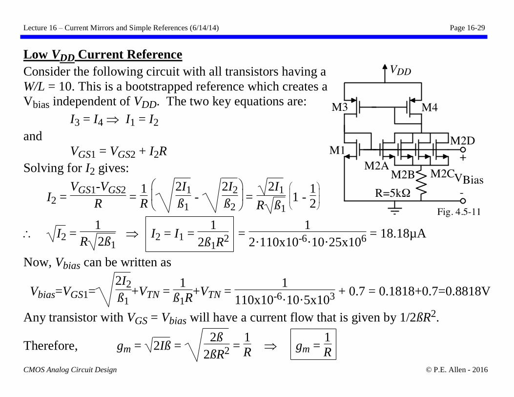
Low VDD Current Reference
Consider the following circuit with all transistors having a
W/L = 10. This is a bootstrapped reference which creates a
Vbias independent of VDD. The two key equations are:
I3 = I4 I1 = I2
and
VGS1 = VGS2 + I2R
Solving for I2 gives:
I2 = VGS1-VGS2
R =
1
R
2I1
ß1 -
2I2
ß2 =
2I1
R ß1
1 - 1
2
I2 = 1
R 2ß1 I2 = I1 =
1
2ß1R2 = 1
2·110x10-6·10·25x106 = 18.18µA
Now, Vbias can be written as
Vbias=VGS1=2I2
ß1+VTN =
1
ß1R+VTN =
1
110x10-6·10·5x103 + 0.7 = 0.1818+0.7=0.8818V
Any transistor with VGS = Vbias will have a current flow that is given by 1/2ßR2.
Therefore, gm = 2Iß = 2ß
2ßR2 = 1
R gm =
1
R
Lecture 16 – Current Mirrors and Simple References (6/14/14) Page 16-30
CMOS Analog Circuit Design © P.E. Allen - 2016
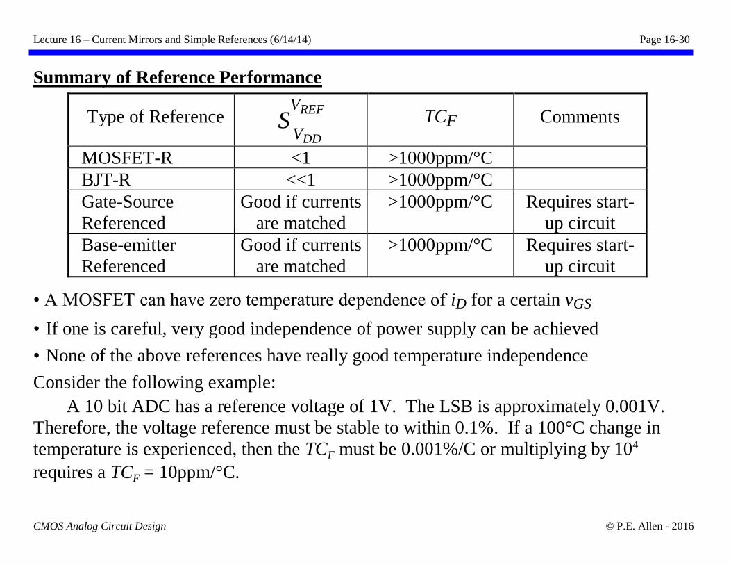
Summary of Reference Performance
Type of Reference S
VREF
VDD
TCF Comments
MOSFET-R <1 >1000ppm/°C
BJT-R <<1 >1000ppm/°C
Gate-Source
Referenced
Good if currents
are matched
>1000ppm/°C Requires start-
up circuit
Base-emitter
Referenced
Good if currents
are matched
>1000ppm/°C Requires start-
up circuit
• A MOSFET can have zero temperature dependence of iD for a certain vGS
• If one is careful, very good independence of power supply can be achieved
• None of the above references have really good temperature independence
Consider the following example:
A 10 bit ADC has a reference voltage of 1V. The LSB is approximately 0.001V.
Therefore, the voltage reference must be stable to within 0.1%. If a 100°C change in
temperature is experienced, then the TCF must be 0.001%/C or multiplying by 104
requires a TCF = 10ppm/°C.